CN1398429A - Communicating device - Google Patents
Communicating deviceDownload PDFInfo
- Publication number
- CN1398429A CN1398429ACN01804798ACN01804798ACN1398429ACN 1398429 ACN1398429 ACN 1398429ACN 01804798 ACN01804798 ACN 01804798ACN 01804798 ACN01804798 ACN 01804798ACN 1398429 ACN1398429 ACN 1398429A
- Authority
- CN
- China
- Prior art keywords
- layer
- compound semiconductor
- communicator
- single crystal
- integrated circuit
- Prior art date
- Legal status (The legal status is an assumption and is not a legal conclusion. Google has not performed a legal analysis and makes no representation as to the accuracy of the status listed.)
- Granted
Links
Images


Classifications
- H—ELECTRICITY
- H01—ELECTRIC ELEMENTS
- H01S—DEVICES USING THE PROCESS OF LIGHT AMPLIFICATION BY STIMULATED EMISSION OF RADIATION [LASER] TO AMPLIFY OR GENERATE LIGHT; DEVICES USING STIMULATED EMISSION OF ELECTROMAGNETIC RADIATION IN WAVE RANGES OTHER THAN OPTICAL
- H01S5/00—Semiconductor lasers
- H01S5/02—Structural details or components not essential to laser action
- H01S5/026—Monolithically integrated components, e.g. waveguides, monitoring photo-detectors, drivers
- H01S5/0261—Non-optical elements, e.g. laser driver components, heaters
- H—ELECTRICITY
- H10—SEMICONDUCTOR DEVICES; ELECTRIC SOLID-STATE DEVICES NOT OTHERWISE PROVIDED FOR
- H10D—INORGANIC ELECTRIC SEMICONDUCTOR DEVICES
- H10D84/00—Integrated devices formed in or on semiconductor substrates that comprise only semiconducting layers, e.g. on Si wafers or on GaAs-on-Si wafers
- H10D84/01—Manufacture or treatment
- H10D84/02—Manufacture or treatment characterised by using material-based technologies
- H10D84/05—Manufacture or treatment characterised by using material-based technologies using Group III-V technology
- C—CHEMISTRY; METALLURGY
- C30—CRYSTAL GROWTH
- C30B—SINGLE-CRYSTAL GROWTH; UNIDIRECTIONAL SOLIDIFICATION OF EUTECTIC MATERIAL OR UNIDIRECTIONAL DEMIXING OF EUTECTOID MATERIAL; REFINING BY ZONE-MELTING OF MATERIAL; PRODUCTION OF A HOMOGENEOUS POLYCRYSTALLINE MATERIAL WITH DEFINED STRUCTURE; SINGLE CRYSTALS OR HOMOGENEOUS POLYCRYSTALLINE MATERIAL WITH DEFINED STRUCTURE; AFTER-TREATMENT OF SINGLE CRYSTALS OR A HOMOGENEOUS POLYCRYSTALLINE MATERIAL WITH DEFINED STRUCTURE; APPARATUS THEREFOR
- C30B25/00—Single-crystal growth by chemical reaction of reactive gases, e.g. chemical vapour-deposition growth
- C30B25/02—Epitaxial-layer growth
- C30B25/18—Epitaxial-layer growth characterised by the substrate
- H—ELECTRICITY
- H01—ELECTRIC ELEMENTS
- H01L—SEMICONDUCTOR DEVICES NOT COVERED BY CLASS H10
- H01L21/00—Processes or apparatus adapted for the manufacture or treatment of semiconductor or solid state devices or of parts thereof
- H01L21/02—Manufacture or treatment of semiconductor devices or of parts thereof
- H01L21/02104—Forming layers
- H01L21/02365—Forming inorganic semiconducting materials on a substrate
- H01L21/02367—Substrates
- H01L21/0237—Materials
- H01L21/02373—Group 14 semiconducting materials
- H01L21/02381—Silicon, silicon germanium, germanium
- H—ELECTRICITY
- H01—ELECTRIC ELEMENTS
- H01L—SEMICONDUCTOR DEVICES NOT COVERED BY CLASS H10
- H01L21/00—Processes or apparatus adapted for the manufacture or treatment of semiconductor or solid state devices or of parts thereof
- H01L21/02—Manufacture or treatment of semiconductor devices or of parts thereof
- H01L21/02104—Forming layers
- H01L21/02365—Forming inorganic semiconducting materials on a substrate
- H01L21/02367—Substrates
- H01L21/02433—Crystal orientation
- H—ELECTRICITY
- H01—ELECTRIC ELEMENTS
- H01L—SEMICONDUCTOR DEVICES NOT COVERED BY CLASS H10
- H01L21/00—Processes or apparatus adapted for the manufacture or treatment of semiconductor or solid state devices or of parts thereof
- H01L21/02—Manufacture or treatment of semiconductor devices or of parts thereof
- H01L21/02104—Forming layers
- H01L21/02365—Forming inorganic semiconducting materials on a substrate
- H01L21/02436—Intermediate layers between substrates and deposited layers
- H01L21/02439—Materials
- H01L21/02469—Group 12/16 materials
- H01L21/02472—Oxides
- H—ELECTRICITY
- H01—ELECTRIC ELEMENTS
- H01L—SEMICONDUCTOR DEVICES NOT COVERED BY CLASS H10
- H01L21/00—Processes or apparatus adapted for the manufacture or treatment of semiconductor or solid state devices or of parts thereof
- H01L21/02—Manufacture or treatment of semiconductor devices or of parts thereof
- H01L21/02104—Forming layers
- H01L21/02365—Forming inorganic semiconducting materials on a substrate
- H01L21/02436—Intermediate layers between substrates and deposited layers
- H01L21/02439—Materials
- H01L21/02488—Insulating materials
- H—ELECTRICITY
- H01—ELECTRIC ELEMENTS
- H01L—SEMICONDUCTOR DEVICES NOT COVERED BY CLASS H10
- H01L21/00—Processes or apparatus adapted for the manufacture or treatment of semiconductor or solid state devices or of parts thereof
- H01L21/02—Manufacture or treatment of semiconductor devices or of parts thereof
- H01L21/02104—Forming layers
- H01L21/02365—Forming inorganic semiconducting materials on a substrate
- H01L21/02436—Intermediate layers between substrates and deposited layers
- H01L21/02494—Structure
- H01L21/02496—Layer structure
- H01L21/02505—Layer structure consisting of more than two layers
- H01L21/02507—Alternating layers, e.g. superlattice
- H—ELECTRICITY
- H01—ELECTRIC ELEMENTS
- H01L—SEMICONDUCTOR DEVICES NOT COVERED BY CLASS H10
- H01L21/00—Processes or apparatus adapted for the manufacture or treatment of semiconductor or solid state devices or of parts thereof
- H01L21/02—Manufacture or treatment of semiconductor devices or of parts thereof
- H01L21/02104—Forming layers
- H01L21/02365—Forming inorganic semiconducting materials on a substrate
- H01L21/02436—Intermediate layers between substrates and deposited layers
- H01L21/02494—Structure
- H01L21/02513—Microstructure
- H—ELECTRICITY
- H01—ELECTRIC ELEMENTS
- H01L—SEMICONDUCTOR DEVICES NOT COVERED BY CLASS H10
- H01L21/00—Processes or apparatus adapted for the manufacture or treatment of semiconductor or solid state devices or of parts thereof
- H01L21/02—Manufacture or treatment of semiconductor devices or of parts thereof
- H01L21/02104—Forming layers
- H01L21/02365—Forming inorganic semiconducting materials on a substrate
- H01L21/02518—Deposited layers
- H01L21/02521—Materials
- H01L21/02538—Group 13/15 materials
- H01L21/02543—Phosphides
- H—ELECTRICITY
- H01—ELECTRIC ELEMENTS
- H01L—SEMICONDUCTOR DEVICES NOT COVERED BY CLASS H10
- H01L21/00—Processes or apparatus adapted for the manufacture or treatment of semiconductor or solid state devices or of parts thereof
- H01L21/02—Manufacture or treatment of semiconductor devices or of parts thereof
- H01L21/02104—Forming layers
- H01L21/02365—Forming inorganic semiconducting materials on a substrate
- H01L21/02518—Deposited layers
- H01L21/02521—Materials
- H01L21/02538—Group 13/15 materials
- H01L21/02546—Arsenides
- H—ELECTRICITY
- H10—SEMICONDUCTOR DEVICES; ELECTRIC SOLID-STATE DEVICES NOT OTHERWISE PROVIDED FOR
- H10D—INORGANIC ELECTRIC SEMICONDUCTOR DEVICES
- H10D84/00—Integrated devices formed in or on semiconductor substrates that comprise only semiconducting layers, e.g. on Si wafers or on GaAs-on-Si wafers
- H10D84/01—Manufacture or treatment
- H10D84/02—Manufacture or treatment characterised by using material-based technologies
- H10D84/08—Manufacture or treatment characterised by using material-based technologies using combinations of technologies, e.g. using both Si and SiC technologies or using both Si and Group III-V technologies
- H—ELECTRICITY
- H10—SEMICONDUCTOR DEVICES; ELECTRIC SOLID-STATE DEVICES NOT OTHERWISE PROVIDED FOR
- H10H—INORGANIC LIGHT-EMITTING SEMICONDUCTOR DEVICES HAVING POTENTIAL BARRIERS
- H10H29/00—Integrated devices, or assemblies of multiple devices, comprising at least one light-emitting semiconductor element covered by group H10H20/00
- H10H29/10—Integrated devices comprising at least one light-emitting semiconductor component covered by group H10H20/00
- H—ELECTRICITY
- H01—ELECTRIC ELEMENTS
- H01L—SEMICONDUCTOR DEVICES NOT COVERED BY CLASS H10
- H01L21/00—Processes or apparatus adapted for the manufacture or treatment of semiconductor or solid state devices or of parts thereof
- H01L21/02—Manufacture or treatment of semiconductor devices or of parts thereof
- H01L21/02104—Forming layers
- H01L21/02107—Forming insulating materials on a substrate
- H01L21/02109—Forming insulating materials on a substrate characterised by the type of layer, e.g. type of material, porous/non-porous, pre-cursors, mixtures or laminates
- H01L21/02112—Forming insulating materials on a substrate characterised by the type of layer, e.g. type of material, porous/non-porous, pre-cursors, mixtures or laminates characterised by the material of the layer
- H01L21/02172—Forming insulating materials on a substrate characterised by the type of layer, e.g. type of material, porous/non-porous, pre-cursors, mixtures or laminates characterised by the material of the layer the material containing at least one metal element, e.g. metal oxides, metal nitrides, metal oxynitrides or metal carbides
- H01L21/02197—Forming insulating materials on a substrate characterised by the type of layer, e.g. type of material, porous/non-porous, pre-cursors, mixtures or laminates characterised by the material of the layer the material containing at least one metal element, e.g. metal oxides, metal nitrides, metal oxynitrides or metal carbides the material having a perovskite structure, e.g. BaTiO3
- H—ELECTRICITY
- H01—ELECTRIC ELEMENTS
- H01L—SEMICONDUCTOR DEVICES NOT COVERED BY CLASS H10
- H01L21/00—Processes or apparatus adapted for the manufacture or treatment of semiconductor or solid state devices or of parts thereof
- H01L21/02—Manufacture or treatment of semiconductor devices or of parts thereof
- H01L21/02104—Forming layers
- H01L21/02107—Forming insulating materials on a substrate
- H01L21/02225—Forming insulating materials on a substrate characterised by the process for the formation of the insulating layer
- H01L21/0226—Forming insulating materials on a substrate characterised by the process for the formation of the insulating layer formation by a deposition process
- H01L21/02263—Forming insulating materials on a substrate characterised by the process for the formation of the insulating layer formation by a deposition process deposition from the gas or vapour phase
- H01L21/02271—Forming insulating materials on a substrate characterised by the process for the formation of the insulating layer formation by a deposition process deposition from the gas or vapour phase deposition by decomposition or reaction of gaseous or vapour phase compounds, i.e. chemical vapour deposition
- H01L21/0228—Forming insulating materials on a substrate characterised by the process for the formation of the insulating layer formation by a deposition process deposition from the gas or vapour phase deposition by decomposition or reaction of gaseous or vapour phase compounds, i.e. chemical vapour deposition deposition by cyclic CVD, e.g. ALD, ALE, pulsed CVD
- H—ELECTRICITY
- H01—ELECTRIC ELEMENTS
- H01L—SEMICONDUCTOR DEVICES NOT COVERED BY CLASS H10
- H01L21/00—Processes or apparatus adapted for the manufacture or treatment of semiconductor or solid state devices or of parts thereof
- H01L21/02—Manufacture or treatment of semiconductor devices or of parts thereof
- H01L21/02104—Forming layers
- H01L21/02365—Forming inorganic semiconducting materials on a substrate
- H01L21/02518—Deposited layers
- H01L21/02521—Materials
- H01L21/02551—Group 12/16 materials
- H01L21/02557—Sulfides
- H—ELECTRICITY
- H01—ELECTRIC ELEMENTS
- H01L—SEMICONDUCTOR DEVICES NOT COVERED BY CLASS H10
- H01L21/00—Processes or apparatus adapted for the manufacture or treatment of semiconductor or solid state devices or of parts thereof
- H01L21/02—Manufacture or treatment of semiconductor devices or of parts thereof
- H01L21/02104—Forming layers
- H01L21/02365—Forming inorganic semiconducting materials on a substrate
- H01L21/02518—Deposited layers
- H01L21/02521—Materials
- H01L21/02551—Group 12/16 materials
- H01L21/0256—Selenides
- H—ELECTRICITY
- H01—ELECTRIC ELEMENTS
- H01L—SEMICONDUCTOR DEVICES NOT COVERED BY CLASS H10
- H01L2924/00—Indexing scheme for arrangements or methods for connecting or disconnecting semiconductor or solid-state bodies as covered by H01L24/00
- H01L2924/0001—Technical content checked by a classifier
- H01L2924/0002—Not covered by any one of groups H01L24/00, H01L24/00 and H01L2224/00
- H—ELECTRICITY
- H01—ELECTRIC ELEMENTS
- H01S—DEVICES USING THE PROCESS OF LIGHT AMPLIFICATION BY STIMULATED EMISSION OF RADIATION [LASER] TO AMPLIFY OR GENERATE LIGHT; DEVICES USING STIMULATED EMISSION OF ELECTROMAGNETIC RADIATION IN WAVE RANGES OTHER THAN OPTICAL
- H01S5/00—Semiconductor lasers
- H01S5/02—Structural details or components not essential to laser action
- H01S5/0206—Substrates, e.g. growth, shape, material, removal or bonding
- H01S5/021—Silicon based substrates
- H—ELECTRICITY
- H10—SEMICONDUCTOR DEVICES; ELECTRIC SOLID-STATE DEVICES NOT OTHERWISE PROVIDED FOR
- H10H—INORGANIC LIGHT-EMITTING SEMICONDUCTOR DEVICES HAVING POTENTIAL BARRIERS
- H10H20/00—Individual inorganic light-emitting semiconductor devices having potential barriers, e.g. light-emitting diodes [LED]
- H10H20/80—Constructional details
- H10H20/81—Bodies
- H10H20/817—Bodies characterised by the crystal structures or orientations, e.g. polycrystalline, amorphous or porous
- H—ELECTRICITY
- H10—SEMICONDUCTOR DEVICES; ELECTRIC SOLID-STATE DEVICES NOT OTHERWISE PROVIDED FOR
- H10H—INORGANIC LIGHT-EMITTING SEMICONDUCTOR DEVICES HAVING POTENTIAL BARRIERS
- H10H20/00—Individual inorganic light-emitting semiconductor devices having potential barriers, e.g. light-emitting diodes [LED]
- H10H20/80—Constructional details
- H10H20/81—Bodies
- H10H20/822—Materials of the light-emitting regions
- H10H20/824—Materials of the light-emitting regions comprising only Group III-V materials, e.g. GaP
Landscapes
- Engineering & Computer Science (AREA)
- Physics & Mathematics (AREA)
- Condensed Matter Physics & Semiconductors (AREA)
- General Physics & Mathematics (AREA)
- Manufacturing & Machinery (AREA)
- Computer Hardware Design (AREA)
- Microelectronics & Electronic Packaging (AREA)
- Power Engineering (AREA)
- Chemical & Material Sciences (AREA)
- Crystallography & Structural Chemistry (AREA)
- Materials Engineering (AREA)
- General Chemical & Material Sciences (AREA)
- Chemical Kinetics & Catalysis (AREA)
- Electromagnetism (AREA)
- Metallurgy (AREA)
- Organic Chemistry (AREA)
- Optics & Photonics (AREA)
- Recrystallisation Techniques (AREA)
- Semiconductor Memories (AREA)
- Metal-Oxide And Bipolar Metal-Oxide Semiconductor Integrated Circuits (AREA)
- Bipolar Integrated Circuits (AREA)
- Junction Field-Effect Transistors (AREA)
- Crystals, And After-Treatments Of Crystals (AREA)
- Semiconductor Lasers (AREA)
- Semiconductor Integrated Circuits (AREA)
- Bipolar Transistors (AREA)
- Formation Of Insulating Films (AREA)
- Solid State Image Pick-Up Elements (AREA)
Abstract
Translated fromChineseDescription
Translated fromChinese技术领域technical field
本发明总体上涉及一种包括半导体尤其是化合物半导体结构的通信装置,以及包括一种单晶化合物半导体材料的半导体结构的制造和用途。The present invention generally relates to a communication device comprising a semiconductor, in particular a compound semiconductor structure, and the manufacture and use of a semiconductor structure comprising a single crystal compound semiconductor material.
背景技术Background technique
大部分半导体分立器件和集成电路是由硅制成的,这至少部分是因为能够得到廉价和高质量的单晶硅衬底。其它半导体材料例如所谓的化合物半导体材料具有的物理特性包括与硅相比更宽的带隙和/或更高的迁移率,或者使得这些材料适用于一定类型半导体器件的直接带隙。不幸的是,化合物半导体材料通常比硅贵很多,并且不能获得与硅一样大的晶片。砷化镓(GaAs)是最容易获得的化合物半导体材料,它只能获得约150毫米(mm)以下直径的晶片。相反,硅晶片可以达到约300mm,普遍可以得到的为200mm。150mm的GaAs晶片比它们的硅等同物贵许多倍。其它化合物半导体材料的晶片更不容易获得,并且比GaAs更贵。Most semiconductor discrete devices and integrated circuits are fabricated from silicon, at least in part because of the availability of inexpensive and high-quality single-crystal silicon substrates. Other semiconductor materials, such as so-called compound semiconductor materials, have physical properties including wider band gaps and/or higher mobility compared to silicon, or direct band gaps that make these materials suitable for certain types of semiconductor devices. Unfortunately, compound semiconductor materials are generally much more expensive than silicon, and wafers as large as silicon are not available. Gallium arsenide (GaAs), the most readily available compound semiconductor material, is only available in wafers with diameters below about 150 millimeters (mm). In contrast, silicon wafers can be up to about 300mm, with 200mm being commonly available. 150mm GaAs wafers are many times more expensive than their silicon equivalents. Wafers of other compound semiconductor materials are less readily available and more expensive than GaAs.
由于化合物半导体材料的理想特性,并且由于它们通常的高额成本以及不容易得到大的尺寸,所以多年来一直致力于在异质衬底上生长化合物半导体材料的薄膜。但是为了实现化合物半导体材料的最佳特性,需要高晶体质量的单晶膜。例如已经尝试在锗、硅和各种绝缘体上生长单晶化合物半导体材料层。这些努力通常是不成功的,因为在基质晶体和生长晶体之间的晶格失配导致所得到的化合物半导体材料薄膜的晶体质量较低。Due to the desirable properties of compound semiconductor materials, and because of their generally high cost and not readily available in large dimensions, efforts have been made for many years to grow thin films of compound semiconductor materials on heterogeneous substrates. But to achieve the best properties of compound semiconductor materials, single crystal films of high crystal quality are required. For example, attempts have been made to grow layers of single crystal compound semiconductor material on germanium, silicon, and various insulators. These efforts were generally unsuccessful because the lattice mismatch between the host crystal and the growing crystal resulted in lower crystalline quality of the resulting thin films of compound semiconductor materials.
如果能够以低成本获得高质量单晶化合物半导体材料的大面积薄膜,则可以以这种膜有效地制造各种半导体器件,成本与在化合物半导体材料大晶片上或在化合物半导体材料大晶片上该材料的外延膜中制造这种器件的成本相比较低。另外,如果高质量单晶化合物半导体材料的薄膜可以在大晶片(bulk wafer)例如硅晶片上实现,就可以获得利用了硅和化合物半导体材料两者优点的集成器件结构。If a large-area thin film of high-quality single-crystal compound semiconductor material can be obtained at low cost, various semiconductor devices can be efficiently manufactured with this film at a cost comparable to that on a large wafer of compound semiconductor material or on a large wafer of compound semiconductor material. The cost of fabricating such devices in epitaxial films of the material is relatively low. Additionally, if thin films of high-quality single-crystal compound semiconductor materials can be realized on bulk wafers such as silicon wafers, integrated device structures that take advantage of the advantages of both silicon and compound semiconductor materials can be obtained.
因此需要一种通信装置,其使用的半导体结构能够提供优于其它单晶材料的高质量单晶化合物半导体膜。There is therefore a need for a communication device using a semiconductor structure capable of providing a high quality single crystal compound semiconductor film superior to other single crystal materials.
附图说明Description of drawings
本发明以实施例的方式进行描述,并且不限于附图,在这些附图中类似的附图标记表示相似的元件。The present invention is described by way of example and is not limited to the accompanying drawings in which like reference numerals refer to like elements.
图1、2、4、5示意性地显示出根据本发明各个实施方案的器件结构的截面图;Figures 1, 2, 4, and 5 schematically show cross-sectional views of device structures according to various embodiments of the present invention;
图3用曲线图显示出可得到的最大膜厚与基质晶体和生长晶体覆盖层间的晶格失配之间的关系;Figure 3 graphically shows the relationship between the maximum obtainable film thickness and the lattice mismatch between the host crystal and the growing crystal cover layer;
图6是通讯装置的一部分的方框图;Fig. 6 is a block diagram of a part of the communication device;
图7-11为部分集成电路的截面图,该集成电路包括一个化合物半导体部分、一个双极部分以及一个MOS部分;并且7-11 are cross-sectional views of portions of integrated circuits including a compound semiconductor portion, a bipolar portion, and a MOS portion; and
图12-18为另一个集成电路的一部分的截面图,该集成电路包括半导体激光器和MOS晶体管。12-18 are cross-sectional views of a portion of another integrated circuit including semiconductor lasers and MOS transistors.
普通技术人员会理解,在图中图示的元件是为了简化和清楚起见,不必按照比例来画出。例如图中一些元件的尺寸可以相对于其它元件放大,以有助于理解本发明的实施方案。Those of ordinary skill will appreciate that elements illustrated in the figures are for simplicity and clarity and have not necessarily been drawn to scale. For example, the dimensions of some of the elements in the figures may be exaggerated relative to other elements to facilitate understanding of embodiments of the present invention.
具体实施方式Detailed ways
图1示意性地显示出根据本发明的一个实施方案的一部分半导体结构20的截面图。半导体结构20包括一个单晶衬底22、包含单晶材料的调节缓冲层(accommodating buffer layer)24以及单晶化合物半导体材料层26。在本文中,“单晶”具有在半导体工业中通常使用的含义。该词指的是单晶体或基本是单晶体的材料,并且包括具有例如在硅或锗或硅锗混合物衬底中通常发现的位错等少量缺陷的那些材料,所述材料还具有在半导体工业中通常发现的这种材料的外延层。Figure 1 schematically shows a cross-sectional view of a portion of a semiconductor structure 20 according to one embodiment of the present invention. Semiconductor structure 20 includes a single crystal substrate 22 , an accommodating buffer layer 24 comprising single crystal material, and a layer 26 of single crystal compound semiconductor material. Herein, "single crystal" has the meaning commonly used in the semiconductor industry. The term refers to a single-crystal or substantially single-crystal material and includes those materials with a small number of defects such as dislocations commonly found in silicon or germanium or silicon-germanium mixture substrates, which also have characteristics commonly found in the semiconductor industry found epitaxial layers of this material.
根据本发明的一个实施方案,结构20也包括位于衬底22和调节缓冲层24之间的无定形中间层28。结构20可以还包括位于调节缓冲层和化合物半导体层26之间的模板层(template layer)30。如以下所详细描述的,模板层有助于引发化合物半导体层在调节缓冲层上的生长。无定形中间层有助于释放调节缓冲层中的应变,这样就有助于高晶体质量的调节缓冲层的生长。According to one embodiment of the present invention, structure 20 also includes an amorphous intermediate layer 28 positioned between substrate 22 and conditioning buffer layer 24 . The structure 20 may further include a template layer 30 between the adjustment buffer layer and the compound semiconductor layer 26 . As described in detail below, the template layer helps to initiate the growth of the compound semiconductor layer on the conditioning buffer layer. The amorphous interlayer helps to release the strain in the conditioning buffer layer, which in turn facilitates the growth of the conditioning buffer layer with high crystalline quality.
根据本发明的一个实施方案,衬底22是单晶半导体晶片,优选是大直径的。该晶片是由周期表中第IV族的材料、优选是IVA族的材料制成。IV族半导体材料的示例包括硅、锗、硅锗混合物硅碳混合物和硅锗碳混合物等。优选的衬底22是含有硅或锗的晶片,最优选是如在半导体工业使用的高质量单晶硅晶片。调节缓冲层24优选外延地生长在下伏衬底上的单晶氧化物或氮化物材料。根据本发明的一个实施方案,无定形中间层28在层24生长期间通过衬底22的氧化作用而生长在衬底22上位于衬底22和生长调节缓冲层24之间的界面处。无定形中间层用于释放在单晶调节缓冲层中因为衬底和缓冲层的晶格常数差异而可能产生的应变。在这里所使用的晶格常数指的是在表面的平面中所测量出的在晶格的各原子之间的距离。如果这种应变没有被无定形中间层所释放,则该应变会导致调节缓冲层的晶体结构缺陷。调节缓冲层晶体结构中的缺陷又会使得难以在单晶化合物半导体层26中获得高质量的晶体结构。According to one embodiment of the invention, substrate 22 is a single crystal semiconductor wafer, preferably of large diameter. The wafer is made of a material of group IV, preferably group IVA, of the periodic table. Examples of Group IV semiconductor materials include silicon, germanium, silicon-germanium-silicon-carbon, silicon-germanium-carbon, and the like. The preferred substrate 22 is a silicon or germanium containing wafer, most preferably a high quality single crystal silicon wafer as used in the semiconductor industry. The conditioning buffer layer 24 is preferably a single crystal oxide or nitride material epitaxially grown on the underlying substrate. According to one embodiment of the present invention, an amorphous intermediate layer 28 is grown on substrate 22 at the interface between substrate 22 and growth regulating buffer layer 24 by oxidation of substrate 22 during growth of layer 24 . The amorphous interlayer is used to relieve strain that may arise in the single crystal conditioning buffer layer due to differences in lattice constants of the substrate and the buffer layer. Lattice constant as used herein refers to the distance between atoms of the crystal lattice measured in the plane of the surface. If this strain is not relieved by the amorphous interlayer, this strain can lead to defects in the crystal structure of the adjusting buffer layer. Adjusting defects in the crystal structure of the buffer layer in turn makes it difficult to obtain a high-quality crystal structure in the single crystal compound semiconductor layer 26 .
调节缓冲层24优选是根据其与下伏衬底和上覆化合物半导体材料的结晶相容性(crystalline compatibility)来选择的单晶氧化物或氮化物材料。例如,该材料可以是其晶格结构与衬底以及与随后覆盖的半导体材料相匹配的氧化物或氮化物。适合作调节缓冲层的材料包括金属氧化物,例如碱土金属钛酸盐、碱土金属锆酸盐、碱土金属铪酸盐、碱土金属钽酸盐、碱土金属钌酸盐、碱土金属铌酸盐、碱土金属钒酸盐、碱土金属锡基钙钛矿(alkaline earth metal tin-based perovskites)、铝酸镧、镧钪氧化物以及氧化钆。另外,各种氮化物例如氮化镓、氮化铝和氮化硼也可以用于调节缓冲层。这些材料中的大多数都是绝缘体,但是例如钌酸锶是导体。一般来说,这些材料是金属氧化物或金属氮化物,更具体地说,这些金属氧化物或氮化物通常包括至少两种不同的金属元素。在一些特定用途中,金属氧化物或氮化物可以包括三种或更多不同的金属元素。Adjustment buffer layer 24 is preferably a single crystal oxide or nitride material selected for its crystalline compatibility with the underlying substrate and overlying compound semiconductor material. For example, the material may be an oxide or nitride whose lattice structure matches that of the substrate and subsequently overlying semiconductor material. Materials suitable for the conditioning buffer layer include metal oxides such as alkaline earth metal titanates, alkaline earth metal zirconates, alkaline earth metal hafnates, alkaline earth metal tantalates, alkaline earth metal ruthenates, alkaline earth metal niobates, alkaline earth Metal vanadates, alkaline earth metal tin-based perovskites, lanthanum aluminate, lanthanum scandium oxide, and gadolinium oxide. In addition, various nitrides such as gallium nitride, aluminum nitride, and boron nitride can also be used to adjust the buffer layer. Most of these materials are insulators, but strontium ruthenate, for example, is a conductor. Generally, these materials are metal oxides or metal nitrides, and more specifically, these metal oxides or nitrides usually include at least two different metal elements. In some specific applications, the metal oxide or nitride may include three or more different metal elements.
无定形中间层28优选是通过衬底22表面的氧化作用形成的氧化物,更优选的是由氧化硅构成。层28的厚度足以释放因为衬底22和调节缓冲层24之间晶格常数不匹配而导致的应变。通常层28的厚度大致在0.5-5nm的范围内。The amorphous intermediate layer 28 is preferably an oxide formed by oxidation of the surface of the substrate 22, more preferably composed of silicon oxide. The thickness of layer 28 is sufficient to relieve the strain caused by the lattice constant mismatch between substrate 22 and tuning buffer layer 24 . Typically the thickness of layer 28 is approximately in the range of 0.5-5 nm.
层26的化合物半导体材料可以根据特定半导体结构的需要而选自下列化合物中的任何一种:IIIA和VA族元素(III-V半导体化合物)、混合的III-V族化合物、II族(A或B)和VIA族元素(II-VI半导体化合物),以及混合的II-VI族化合物。示例包括砷化镓(GaAs)、砷化镓铟(GaInAs)、砷化镓铝(GaAlAs)、磷化铟(InP)、硫化镉(CdS)、碲化镉汞(CdHgTe)、硒化锌(ZnSe)、硒化硫锌(Zinc sulfur selenide,ZnSSe)等。适合的模板材料在选定位置通过化学键结合在调节缓冲层的表面上,并提供用于随后化合物半导体层26的外延生长的成核位置。模板30的适当材料如下所述。The compound semiconductor material of layer 26 can be selected from any of the following compounds according to the needs of the particular semiconductor structure: IIIA and VA group elements (III-V semiconductor compounds), mixed III-V group compounds, group II (A or B) and group VIA elements (II-VI semiconductor compounds), and mixed group II-VI compounds. Examples include gallium arsenide (GaAs), gallium indium arsenide (GaInAs), gallium aluminum arsenide (GaAlAs), indium phosphide (InP), cadmium sulfide (CdS), cadmium mercury telluride (CdHgTe), zinc selenide ( ZnSe), zinc sulfur selenide (Zinc sulfur selenide, ZnSSe), etc. A suitable template material is chemically bonded on the surface of the conditioning buffer layer at selected locations and provides nucleation sites for subsequent epitaxial growth of the compound semiconductor layer 26 . Suitable materials for template 30 are described below.
图2显示出根据本发明再一个实施方案的一部分半导体结构40的截面图。结构40类似于前述半导体结构20,但是在调节缓冲层24和单晶化合物半导体材料层26之间还设置了附加缓冲层32。具体地说,附加缓冲层32位于模板层30和上覆化合物半导体材料层之间。由半导体或化合物半导体材料形成的附加缓冲层用于在调节缓冲层的晶格常数与上覆单晶化合物半导体材料层之间不能充分匹配时提供晶格补偿。FIG. 2 shows a cross-sectional view of a portion of a semiconductor structure 40 according to yet another embodiment of the present invention. The structure 40 is similar to the aforementioned semiconductor structure 20 , but with an additional buffer layer 32 disposed between the regulating buffer layer 24 and the layer 26 of single crystal compound semiconductor material. Specifically, the additional buffer layer 32 is located between the template layer 30 and the overlying compound semiconductor material layer. An additional buffer layer formed of a semiconductor or compound semiconductor material is used to provide lattice compensation when the lattice constant of the tuned buffer layer is not sufficiently matched to the overlying layer of single crystal compound semiconductor material.
以下非限制性的示例实施例阐述了可以用于根据本发明不同实施方案的结构20和结构40的材料的各种组合。这些实施例只作为示例之用,本发明不限于这些示例性实施例。The following non-limiting illustrative examples illustrate various combinations of materials that may be used in structures 20 and 40 according to various embodiments of the invention. These examples are for illustration only, and the present invention is not limited to these example examples.
实施例1Example 1
根据本发明的一个实施方案,单晶衬底22是沿着(100)方向取向的硅衬底。该硅衬底可以是例如在制造互补金属氧化物半导体(CMOS)集成电路中通常使用的直径约为200-300nm的硅衬底。根据本发明的这个实施方案,调节缓冲层24是SrzBa1-zTiO3单晶层,其中z是0-1,无定形中间层是在硅衬底和调节缓冲层之间的界面处形成的氧化硅(SiOx)层。对z值进行选择,以获得一个或多个与随后形成的层26的对应晶格常数密切匹配的晶格常数。调节缓冲层厚度可以约是2-100纳米(nm),优选的厚度是约10nm。通常,希望调节缓冲层的厚度足以将化合物半导体层与衬底隔离,以获得理想的电学和光学性能。大于100nm的层厚度通常很少能提供更多的优点,但是成本却不必要的增加;但是如果需要可以制造较厚的层。氧化硅无定形中间层的厚度约为0.5-5nm,优选的厚度是1.5-2.5nm。According to one embodiment of the present invention, single crystal substrate 22 is a silicon substrate oriented along the (100) direction. The silicon substrate may be, for example, a silicon substrate with a diameter of approximately 200-300 nm commonly used in the manufacture of complementary metal-oxide-semiconductor (CMOS) integrated circuits. According to this embodiment of the invention, the adjustment buffer layer 24 is a Srz Ba1-z TiO3 single crystal layer, where z is 0-1, and the amorphous interlayer is at the interface between the silicon substrate and the adjustment buffer layer A silicon oxide (SiOx) layer is formed. The z value is selected to obtain one or more lattice constants that closely match the corresponding lattice constant of the subsequently formed layer 26 . The thickness of the adjustment buffer layer can be about 2-100 nanometers (nm), with a preferred thickness of about 10 nm. In general, it is desirable to adjust the thickness of the buffer layer sufficiently to isolate the compound semiconductor layer from the substrate to obtain desired electrical and optical properties. Layer thicknesses greater than 100 nm generally offer little further advantage at unnecessarily high cost; however thicker layers can be fabricated if desired. The thickness of the silicon oxide amorphous interlayer is about 0.5-5 nm, preferably 1.5-2.5 nm.
根据该实施方案,化合物半导体材料层26是砷化镓(GaAs)或砷化铝镓(AlGaAs)层,厚度是约1nm-约100μm,优选厚度是约0.5μm-10μm。厚度通常取决于所制备的层的应用。为了便于砷化镓或砷化铝镓在单晶氧化物上的外延生长,通过覆盖氧化物层而形成一个模板层。模板层优选是Ti-As、Sr-O-As、Sr-Ga-O或Sr-Al-O的1-10个单层。作为优选实施例,Ti-As和Sr-Ga-O的1-2个单层已经表明能成功生长GaAs层。According to this embodiment, compound semiconductor material layer 26 is a gallium arsenide (GaAs) or aluminum gallium arsenide (AlGaAs) layer having a thickness of about 1 nm to about 100 μm, preferably a thickness of about 0.5 μm to 10 μm. The thickness generally depends on the application of the layer being produced. In order to facilitate the epitaxial growth of GaAs or AlGaAs on single crystal oxide, a template layer is formed by covering the oxide layer. The template layer is preferably 1-10 monolayers of Ti-As, Sr-O-As, Sr-Ga-O or Sr-Al-O. As a preferred example, 1-2 monolayers of Ti-As and Sr-Ga-O have been shown to successfully grow GaAs layers.
实施例2Example 2
根据本发明的再一个实施方案,单晶衬底22是如上所述的硅衬底。调节缓冲层是立方晶相或斜方晶相的锶或钡的锆酸盐或铪酸盐单晶氧化物,氧化硅无定形中间层在硅衬底和调节缓冲层之间的界面处形成。调节缓冲层的厚度是约2-100nm,优选是至少5nm,以确保足够的结晶和表面质量,它由单晶SrZrO3、BaZrO3、SrHfO3、BaSnO3或BaHfO3形成。例如BaZrO3单晶氧化物层可以在约700摄氏度生长。所形成的氧化物晶体的晶格结构相对于衬底硅晶格结构表现出45度的旋转。According to yet another embodiment of the present invention, the single crystal substrate 22 is a silicon substrate as described above. The adjustment buffer layer is a zirconate or hafnate single crystal oxide of strontium or barium in a cubic or orthorhombic phase, and an amorphous intermediate layer of silicon oxide is formed at the interface between the silicon substrate and the adjustment buffer layer. The thickness of the buffer layer is adjusted to be about 2-100 nm, preferably at least 5 nm, to ensure sufficient crystallinity and surface quality, which is formed of single crystal SrZrO3 , BaZrO3 , SrHfO3 , BaSnO3 or BaHfO3 . For example BaZrO3 single crystal oxide layers can be grown at about 700°C. The lattice structure of the formed oxide crystal exhibits a 45 degree rotation relative to the substrate silicon lattice structure.
这些锆酸盐或铪酸盐材料形成的调节缓冲层适合于在磷化铟(InP)系统中生长化合物半导体材料。化合物半导体材料可以是例如磷化铟(InP)或砷化铟镓(InGaAs),厚度约为1.0nm-10μm。适合于这种结构的模板是锆-砷(Zr-As)、锆-磷(Zr-P)、铪-砷(Hf-As)、铪-磷(Hf-P)、锶-氧-砷(Sr-O-As)、锶-氧-磷(Sr-O-P)、钡-氧-砷(Ba-O-As)、铟-锶-氧(In-Sr-O)、或钡-氧-磷(Ba-O-P)的1-10个单层,优选是这些材料之一的1-2个单层。举例来说,对于锆酸钡调节缓冲层来说,表面是锆的1-2个单层,然后沉积砷的1-2个单层,以形成Zr-As模板。然后来自磷化铟系统的化合物半导体材料的单晶层在该模板层上生长。所得到的化合物半导体材料的晶格结构相对于调节缓冲层晶格结构表现出45度的旋转,并且与(100)InP的晶格失配小于2.5%,优选小于1.0%。The adjustment buffer layer formed by these zirconate or hafnate materials is suitable for growing compound semiconductor materials in an indium phosphide (InP) system. The compound semiconductor material can be, for example, indium phosphide (InP) or indium gallium arsenide (InGaAs), with a thickness of about 1.0 nm-10 μm. Suitable templates for this structure are zirconium-arsenic (Zr-As), zirconium-phosphorus (Zr-P), hafnium-arsenic (Hf-As), hafnium-phosphorous (Hf-P), strontium-oxygen-arsenic ( Sr-O-As), strontium-oxygen-phosphorus (Sr-O-P), barium-oxygen-arsenic (Ba-O-As), indium-strontium-oxygen (In-Sr-O), or barium-oxygen-phosphorus 1-10 monolayers of (Ba-O-P), preferably 1-2 monolayers of one of these materials. For example, for a barium zirconate conditioning buffer layer, the surface is 1-2 monolayers of zirconium, then 1-2 monolayers of arsenic are deposited to form the Zr-As template. A single crystal layer of compound semiconductor material from the indium phosphide system is then grown on this template layer. The lattice structure of the resulting compound semiconductor material exhibits a 45 degree rotation with respect to the lattice structure of the regulating buffer layer, and has a lattice mismatch with (100) InP of less than 2.5%, preferably less than 1.0%.
实施例3Example 3
根据本发明的再一个实施方案,提供一种结构,它适合于覆盖硅衬底的II-VI族材料外延膜的生长。该衬底优选是上述硅晶片。适合的调节缓冲层材料是SrxBa1-xTiO3,其中x是0-1,厚度约为2-100nm,优选是5-15nm。II-VI族化合物半导体材料可以是例如硒化锌(ZnSe)或硒化硫锌(ZnSSe)。适合于这种材料系统的模板包括锌-氧(Zn-O)的1-10个单层,然后是过量的锌的1-2个单层,然后在表面上对锌进行硒化。或者模板可以是例如锶-硫(Sr-S),然后是ZnSeS。According to yet another embodiment of the present invention, a structure is provided which is suitable for the growth of an epitaxial film of a Group II-VI material overlying a silicon substrate. The substrate is preferably the aforementioned silicon wafer. A suitable adjustment buffer layer material is Srx Ba1-x TiO3 , where x is 0-1, with a thickness of about 2-100 nm, preferably 5-15 nm. The group II-VI compound semiconductor material may be, for example, zinc selenide (ZnSe) or zinc sulfur selenide (ZnSSe). Suitable templates for this material system include 1-10 monolayers of zinc-oxygen (Zn-O), followed by 1-2 monolayers of excess zinc, followed by selenization of the zinc on the surface. Or the template could be eg strontium-sulfur (Sr-S) followed by ZnSeS.
实施例4Example 4
本发明的该实施方案是图2所示结构40的示例。衬底22、单晶氧化物层24以及单晶化合物半导体材料层26可以与上述实施例1类似。另外,附加缓冲层32用于减轻可能因为调节缓冲层的晶格和单晶半导体材料的晶格的不匹配而导致的任何应变。缓冲层32可以是磷砷化镓(GaAsxP1-x)或磷化铟镓(InyGa1-yP)应变补偿超晶格(straincompensated superlattice)。在磷砷化镓超晶格中x为0-1,在磷化铟镓超晶格中y为0-1。通过根据情况改变x或y的值,晶格常数会从底部至顶部穿过超晶格而变化,形成下伏氧化物和上覆化合物半导体材料之间晶格常数的匹配。超晶格的厚度约为50-500nm,优选的厚度是200-100nm。这种结构的模板可以与实施例1所述的相同。或者,缓冲层可以是单晶锗层,厚度是1-50nm,优选约为2-20nm。在使用锗缓冲层时,可以使用锗-锶(Ge-Sr)或锗-钛(Ge-Ti)模板层,厚度约为1个单层。该氧化物层被覆盖了锶的单层或钛的单层,以作为随后单晶锗沉积的成核位置。锶或钛单层提供了锗的第一单层可以键连的成核位置。This embodiment of the invention is an example of structure 40 shown in FIG. 2 . The substrate 22 , the single crystal oxide layer 24 and the single crystal compound semiconductor material layer 26 may be similar to those in Embodiment 1 above. In addition, the additional buffer layer 32 serves to relieve any strain that may be caused by a mismatch between the crystal lattice of the conditioning buffer layer and the crystal lattice of the single crystal semiconductor material. The buffer layer 32 may be a gallium arsenide phosphide (GaAsx P1-x ) or an indium gallium phosphide (Iny Ga1-y P) strain compensated superlattice. In the gallium arsenide phosphide superlattice, x is 0-1, and in the indium gallium phosphide superlattice, y is 0-1. By changing the value of x or y as the case may be, the lattice constant changes from bottom to top across the superlattice, creating a lattice constant match between the underlying oxide and the overlying compound semiconductor material. The thickness of the superlattice is about 50-500 nm, preferably 200-100 nm. The template for this structure can be the same as described in Example 1. Alternatively, the buffer layer can be a single crystal germanium layer with a thickness of 1-50 nm, preferably about 2-20 nm. When a germanium buffer layer is used, a germanium-strontium (Ge-Sr) or germanium-titanium (Ge-Ti) template layer can be used, with a thickness of about 1 monolayer. This oxide layer is covered with a monolayer of strontium or a monolayer of titanium to serve as nucleation sites for the subsequent deposition of single crystal germanium. The strontium or titanium monolayer provides nucleation sites to which the first monolayer of germanium can bond.
实施例5Example 5
该实施例也阐释可用于图2所示结构40的材料。衬底材料22、调节缓冲层24、单晶化合物半导体材料层26以及模板层30可以与上述实施例2类似。另外,在调节缓冲层和上覆单晶化合物半导体材料层之间插入一个缓冲层32。该缓冲层,即又一种单晶半导体材料可以是例如砷化铟镓(InGaAs)的递变层,其中铟组分在0-47%之间变化。该缓冲层优选的厚度约为10-30nm。使缓冲层的组成从GaAs到InGaAs变化用来提供下伏单晶氧化物材料和上覆单晶化合物半导体材料层之间的晶格匹配。如果在调节缓冲层24和单晶化合物半导体材料层26之间存在晶格失配,这种缓冲层就特别有用。This example also illustrates materials that can be used for structure 40 shown in FIG. 2 . The substrate material 22 , the adjustment buffer layer 24 , the single crystal compound semiconductor material layer 26 and the template layer 30 may be similar to those in the second embodiment above. In addition, a buffer layer 32 is interposed between the adjustment buffer layer and the overlying single crystal compound semiconductor material layer. The buffer layer, yet another monocrystalline semiconductor material, may be a graded layer of, for example, indium gallium arsenide (InGaAs), where the indium composition varies between 0-47%. The buffer layer preferably has a thickness of about 10-30 nm. Varying the composition of the buffer layer from GaAs to InGaAs serves to provide lattice matching between the underlying single crystal oxide material and the overlying single crystal compound semiconductor material layer. Such a buffer layer is particularly useful if there is a lattice mismatch between the adjustment buffer layer 24 and the layer 26 of single crystal compound semiconductor material.
再参考图1和2,衬底22是单晶衬底,例如单晶硅衬底。单晶衬底的晶体结构以晶格常数和晶格取向为特征。类似地,调节缓冲层24也是单晶材料,该单晶材料的晶格也以晶格常数和晶格取向为特征。调节缓冲层和单晶衬底的晶格常数必须严格匹配,或者必须是这样,即在一个晶格取向相对于另一个晶格取向旋转时可实现晶格常数的基本匹配。在这里,“基本相等”和“基本匹配”表示晶格常数之间存在足够的相似性,从而允许高质量的晶体层在下伏层上生长。Referring again to Figures 1 and 2, substrate 22 is a single crystal substrate, such as a single crystal silicon substrate. The crystal structure of a single crystal substrate is characterized by a lattice constant and a lattice orientation. Similarly, the adjustment buffer layer 24 is also a single crystal material whose crystal lattice is also characterized by a lattice constant and a lattice orientation. The lattice constants of the tuning buffer layer and the single crystal substrate must be closely matched, or must be such that a substantial match of lattice constants can be achieved when one lattice orientation is rotated relative to the other. Here, "substantially equal" and "substantially match" indicate that there is sufficient similarity between the lattice constants to allow a high-quality crystalline layer to grow on the underlying layer.
图3通过曲线图显示出高晶体质量的生长晶体层可实现的厚度与基质晶体和生长晶体晶格常数间的不匹配之间的函数关系。曲线42表示高晶体质量材料的边界。曲线42右面的区域表示易于成为多晶体的层。在没有晶格失配的情况中,理论上可以在基质晶体上生长出无限厚的高质量外延层。随着在晶格常数中不匹配的增加,可以获得的高质量晶体层的厚度迅速降低。作为参考点,例如,如果基质晶体和生长晶体之间晶格常数不匹配高于约2%,则不能获得超过约20nm的单晶外延层。Figure 3 graphically shows the achievable thickness of a grown crystal layer of high crystal quality as a function of the mismatch between the lattice constants of the host crystal and the grown crystal. Curve 42 represents the boundary for high crystalline quality material. The area to the right of curve 42 represents layers that tend to become polycrystalline. In the absence of lattice mismatch, it is theoretically possible to grow infinitely thick high-quality epitaxial layers on host crystals. As the mismatch in lattice constants increases, the thickness of achievable high-quality crystalline layers decreases rapidly. As a point of reference, for example, if the lattice constant mismatch between the host crystal and the growing crystal is higher than about 2%, single crystal epitaxial layers beyond about 20 nm cannot be obtained.
根据本发明的一个实施方案,衬底22是(100)或(111)取向的单晶硅晶片,并且调节缓冲层24是钛酸锶钡层。这两种材料之间晶格常数的基本匹配是通过将钛酸盐材料的晶体取向相对于硅衬底晶片的晶体取向旋转45°而获得的。在该结构中包含无定形中间层24(在此实施例中是氧化硅层)用来减少在钛酸盐单晶层中可能因为基质硅晶片和生长的钛酸盐层之间的不匹配而导致的应变。结果,根据本发明的一个实施方案,可以获得高质量的厚单晶钛酸盐层。According to one embodiment of the present invention, substrate 22 is a (100) or (111) oriented single crystal silicon wafer, and adjustment buffer layer 24 is a barium strontium titanate layer. The substantial matching of lattice constants between the two materials was obtained by rotating the crystal orientation of the titanate material by 45° with respect to the crystal orientation of the silicon substrate wafer. The inclusion of an amorphous intermediate layer 24 (in this embodiment a silicon oxide layer) in the structure serves to reduce the potential for mismatch in the titanate single crystal layer due to mismatch between the host silicon wafer and the growing titanate layer. resulting strain. As a result, according to one embodiment of the present invention, a high-quality thick monocrystalline titanate layer can be obtained.
仍然参考图1和2,层26是外延生长的单晶化合物半导体材料层,该晶体材料也以晶体晶格常数和晶体取向为特征。为了在这种外延生长层中获得高晶体质量,调节缓冲层必须具有高晶体质量。另外,为了在层26中获得高晶体质量,希望基质晶体(在这种情况下是单晶调节缓冲层)与生长晶体之间的晶体晶格常数基本匹配。利用适当选择的材料,通过生长晶体的晶体取向相对于基质晶体的晶体取向的旋转,可以获得晶格常数的基本匹配。如果生长晶体是砷化镓、砷化铝镓、硒化锌、或硒化硫锌并且调节缓冲层是单晶SrxBa1-xTiO3,则可以实现两种材料之间晶体晶格常数的基本匹配,其中生长层的晶体取向相对于基质单晶氧化物的取向旋转45°。同样,如果基质材料是锶或钡的锆酸盐或者锶或钡的铪酸盐或氧化钡锡,并且化合物半导体层是磷化铟或砷化镓铟或砷化铝铟,通过将生长晶体层的取向相对于基质氧化物晶体的取向旋转45°,可以获得晶体晶格常数的基本匹配。在一些情况中,基质氧化物和生长的化合物半导体层之间的晶体半导体缓冲层可以用来减少在生长的单晶化合物半导体层中因为晶格常数的微小差异而可能产生的应变。因此可以在生长的单晶化合物半导体层中获得较好的晶体质量。Still referring to FIGS. 1 and 2 , layer 26 is an epitaxially grown layer of single crystal compound semiconductor material that is also characterized by a crystal lattice constant and crystal orientation. In order to obtain high crystalline quality in such epitaxially grown layers, the conditioning buffer layer must have high crystalline quality. Additionally, in order to achieve high crystal quality in layer 26, it is desirable to substantially match the crystal lattice constants between the host crystal (in this case the single crystal conditioning buffer layer) and the growing crystal. With proper choice of materials, substantial matching of lattice constants can be obtained by rotation of the crystal orientation of the growing crystal relative to that of the host crystal. If the growing crystal is GaAs, AlGaAs, ZnSe, or ZnSSe and the regulating buffer layer is single crystal Srx Ba1-x TiO3 , a crystal lattice constant between the two materials can be achieved , where the crystallographic orientation of the grown layer is rotated by 45° relative to that of the host single-crystal oxide. Likewise, if the host material is zirconate of strontium or barium or hafnate of strontium or barium or barium tin oxide, and the compound semiconductor layer is indium phosphide or gallium indium arsenide or aluminum indium arsenide, by growing the crystal layer Rotating the orientation of the crystals by 45° with respect to the orientation of the host oxide crystals, a substantial match of the crystal lattice constants can be obtained. In some cases, a crystalline semiconductor buffer layer between the host oxide and the grown compound semiconductor layer can be used to reduce strain that may arise in the grown single crystalline compound semiconductor layer due to small differences in lattice constant. A better crystal quality can thus be obtained in the grown single crystal compound semiconductor layer.
以下实施例阐述了根据本发明的一个实施方案用于制造半导体结构例如图1和2所示结构的工艺。该工艺一开始提供包括硅或锗的单晶半导体衬底。根据本发明的优选实施方案,半导体衬底是具有(100)取向的硅晶片。衬底的取向优选在晶轴上或至多偏离晶轴约0.5°。至少部分半导体衬底具有裸露的表面,但是该衬底的其它部分如下所述可围绕着其它结构。“裸露”一词在本文中表示该部分衬底中的表面已经被清洁从而除去了任何氧化物、杂质或外来物质。众所周知,裸露的硅具有高反应性,易于形成天然氧化物。“裸露”的含义包括这种天然氧化物。也可以有意在半导体衬底上生长出薄的氧化硅,但是这种生长的氧化物对于本发明的工艺不是必要的。为了外延生长出覆盖该单晶衬底的单晶氧化物层,必须首先除去天然氧化物层以将下伏衬底的晶体结构暴露出来。以下过程优选通过分子束外延附生(molecular beam epitaxy,MBE)来进行。可以通过在MBE设备中首先热沉积薄薄的一层锶来除去天然氧化物。然后将该衬底加热至约为750°,以使得锶与天然氧化硅层反应。锶用来减少氧化硅以留下没有硅氧化物的表面。所得到的具有有序的2×1结构的表面包括锶、氧和硅。该有序的2×1结构形成用于单晶氧化物覆盖层的有序生长的模板。该模板具有必要的化学和物理性能,以为覆盖层的晶体生长成核。The following example illustrates a process for fabricating a semiconductor structure such as that shown in FIGS. 1 and 2 according to one embodiment of the invention. The process initially provides a single crystal semiconductor substrate comprising silicon or germanium. According to a preferred embodiment of the invention, the semiconductor substrate is a silicon wafer with (100) orientation. The orientation of the substrate is preferably on the crystallographic axis or at most about 0.5° off the crystallographic axis. At least part of the semiconductor substrate has an exposed surface, but other parts of the substrate may be surrounded by other structures as described below. The term "bare" is used herein to indicate that the surface in the portion of the substrate has been cleaned to remove any oxides, impurities or foreign matter. Bare silicon is known to be highly reactive and prone to the formation of native oxides. The meaning of "bare" includes such native oxides. Thin silicon oxide may also be intentionally grown on the semiconductor substrate, but such grown oxide is not necessary for the process of the invention. In order to epitaxially grow a single crystalline oxide layer overlying the single crystalline substrate, the native oxide layer must first be removed to expose the crystalline structure of the underlying substrate. The following process is preferably performed by molecular beam epitaxy (MBE). Native oxides can be removed by first thermally depositing a thin layer of strontium in MBE equipment. The substrate is then heated to about 750° to cause the strontium to react with the native silicon oxide layer. Strontium is used to reduce silicon oxide to leave a surface free of silicon oxide. The resulting surface with an ordered 2x1 structure includes strontium, oxygen and silicon. This ordered 2x1 structure forms the template for the ordered growth of the single crystal oxide capping layer. This template has the necessary chemical and physical properties to nucleate the crystal growth of the overlying layer.
根据本发明的可选实施方案,天然氧化硅可以被转化,并且可以通过在低温下利用MBE将氧化锶沉积到衬底表面上并随后将衬底加热至约750°而加工衬底表面,以用于单晶氧化层生长。在这个温度下,在氧化锶和天然氧化硅之间发生固态反应,从而导致天然氧化硅的减少并留下有序的2×1结构,其衬底表面残留有锶、氧和硅。同样,这形成用于随后有序单晶氧化物层生长的模板。According to an alternative embodiment of the present invention, native silicon oxide can be converted and the substrate surface can be processed by depositing strontium oxide onto the substrate surface using MBE at low temperature and subsequently heating the substrate to about 750° to For single crystal oxide layer growth. At this temperature, a solid-state reaction occurs between strontium oxide and native silicon oxide, resulting in a reduction of native silicon oxide and leaving an ordered 2×1 structure with residual strontium, oxygen, and silicon on the substrate surface. Again, this forms a template for the subsequent growth of the ordered single crystal oxide layer.
在从衬底表面除去氧化硅之后,根据本发明的一个实施方案,将衬底冷却到约400-600℃的温度,通过分子束外延附生在模板层上生长钛酸锶层。通过打开MBE设备中的遮挡板(shutter)以暴露出锶、钛和氧源从而开始MBE过程。锶和钛的比例大致为1∶1。氧分压一开始设定为最小值,从而使化学计量的钛酸锶以大约0.3-0.5nm/分钟的速度生长。在钛酸锶开始生长之后,将氧分压提高至最初的最小值之上。氧的过压导致无定形氧化硅层在下伏衬底和正在生长的钛酸锶层之间的界面处生长。氧化硅层的生长其原因在于氧通过正在生长的钛酸锶层扩散至所述界面处,在该界面处,氧与硅在下伏衬底的表面处反应。钛酸锶生长成为有序的单晶,并且晶体取向相对于下伏衬底的有序2×1晶体结构旋转45°。由于硅衬底和生长的晶体之间晶格常数的微小不匹配而可能存在于钛酸锶层中的应变在无定形氧化硅中间层中被释放。After silicon oxide is removed from the substrate surface, according to one embodiment of the present invention, the substrate is cooled to a temperature of about 400-600° C., and a strontium titanate layer is epitaxially grown on the template layer by molecular beam epitaxy. The MBE process was started by opening the shutter in the MBE apparatus to expose the strontium, titanium and oxygen sources. The ratio of strontium to titanium is approximately 1:1. The oxygen partial pressure was initially set to a minimum value so that stoichiometric strontium titanate grew at a rate of about 0.3-0.5 nm/min. After the growth of strontium titanate begins, the oxygen partial pressure is raised above the initial minimum. The overpressure of oxygen causes the growth of an amorphous silicon oxide layer at the interface between the underlying substrate and the growing strontium titanate layer. The growth of the silicon oxide layer results from the diffusion of oxygen through the growing strontium titanate layer to the interface where it reacts with the silicon at the surface of the underlying substrate. Strontium titanate grows as an ordered single crystal with a crystal orientation rotated by 45° relative to the ordered 2×1 crystal structure of the underlying substrate. Strain that may exist in the strontium titanate layer due to a slight mismatch in lattice constant between the silicon substrate and the growing crystal is released in the amorphous silicon oxide interlayer.
在钛酸锶层生长到所需厚度之后,用模板层将单晶钛酸锶盖住,该模板层有助于所需化合物半导体材料的外延层的随后的生长。为了砷化镓外延层的随后生长,可以通过利用1-2个钛单层、1-2个钛-氧单层或1-2个锶-氧单层来终止生长,从而压盖钛酸锶单晶层的MBE生长。在该压盖层形成之后,沉积砷以形成Ti-As键、Ti-O-As键或Sr-O-As键。这其中的任何一个都可以形成适合用于砷化镓单晶层的沉积和形成的模板。在该模板形成之后,将镓引入与砷进行反应,从而形成砷化镓。或者,可以将镓沉积在压盖层上,以形成Sr-O-Ga键,将砷引入和镓形成GaAs。After the strontium titanate layer is grown to the desired thickness, the single crystal strontium titanate is capped with a template layer which facilitates the subsequent growth of an epitaxial layer of the desired compound semiconductor material. For subsequent growth of the GaAs epitaxial layer, the growth can be terminated by utilizing 1-2 Ti monolayers, 1-2 Ti-Oxygen monolayers, or 1-2 Sr-Oxygen monolayers to cap the SrTitanate MBE growth of single crystal layers. After the capping layer is formed, arsenic is deposited to form Ti-As bonds, Ti-O-As bonds or Sr-O-As bonds. Any of these can form a suitable template for the deposition and formation of gallium arsenide single crystal layers. After this template is formed, gallium is introduced to react with arsenic to form gallium arsenide. Alternatively, gallium can be deposited on the capping layer to form Sr-O-Ga bonds, introducing arsenic and gallium to form GaAs.
图2所示结构可以利用上述方法形成,但是还包括附加缓冲层沉积步骤。在沉积单晶化合物半导体层之前,形成覆盖模板层的缓冲层。如果缓冲层是化合物半导体超晶格,可以通过例如MBE来将这种超晶格沉积在上述模板上。如果缓冲层是锗层,则上述工艺应当改为用锶或钛的最终层压盖钛酸锶单晶层,然后通过沉积锗而使其与锶或钛反应。然后可以将锗缓冲层直接沉积在该模板上。The structure shown in Figure 2 can be formed using the methods described above, but including an additional buffer layer deposition step. Before depositing the single crystal compound semiconductor layer, a buffer layer covering the template layer is formed. If the buffer layer is a compound semiconductor superlattice, this superlattice can be deposited on the aforementioned template by eg MBE. If the buffer layer is a germanium layer, the above process should be changed to cap the strontium titanate single crystal layer with a final layer of strontium or titanium, which is then reacted with strontium or titanium by depositing germanium. A germanium buffer layer can then be deposited directly on the template.
上述工艺阐述了用于通过分子束外延附生形成包括硅衬底、单晶钛酸锶调节缓冲层以及单晶砷化镓化合物半导体层的半导体结构的方法。该过程可以通过化学汽相淀积(CVD)、金属有机化学汽相淀积(MOCVD)、迁移增强外延附生(migration enhanced epitaxy,MEE)、原子层外延附生(atomic layer epitaxy,ALE)等方法来进行。另外,通过类似的方法,可以生长其它的单晶调节缓冲层,例如碱土金属钛酸盐、锆酸盐、铪酸盐、钽酸盐、钒酸盐、钌酸盐和铌酸盐,碱土金属锡基钙钛矿,铝酸镧,氧化镧钪,以及氧化钆。另外,通过类似的方法例如MBE,可以沉积其它III-V和II-VI族单晶化合物半导体层,覆盖所述单晶氧化物调节缓冲层。The process described above illustrates a method for forming a semiconductor structure comprising a silicon substrate, a single crystal strontium titanate conditioning buffer layer, and a single crystal gallium arsenide compound semiconductor layer by molecular beam epitaxy. The process can be achieved through chemical vapor deposition (CVD), metal organic chemical vapor deposition (MOCVD), migration enhanced epitaxy (MEE), atomic layer epitaxy (ALE), etc. method to proceed. In addition, other single-crystal conditioning buffer layers can be grown by similar methods, such as alkaline earth metal titanates, zirconates, hafnates, tantalates, vanadates, ruthenates and niobates, alkaline earth metal Tin-based perovskites, lanthanum aluminate, lanthanum scandium oxide, and gadolinium oxide. In addition, other III-V and II-VI single crystal compound semiconductor layers can be deposited by similar methods such as MBE, covering the single crystal oxide regulating buffer layer.
化合物半导体材料和单晶氧化物调节缓冲层的每个变型采用了适当的模板,用于引发化合物半导体层的生长。例如,如果调节缓冲层是碱土金属锆酸盐,该氧化物可以由薄的锆层所压盖。沉积锆之后可以沉积与锆反应的砷或磷,作为分别沉积砷化铟镓、砷化铟铝或磷化铟的前体。类似地,如果单晶氧化物调节缓冲层是碱土金属铪酸盐,该氧化物层可以由铪的薄层所压盖。沉积铪之后,沉积与铪反应的砷或磷,作为分别生长砷化铟镓、砷化铟铝或磷化铟层的前体。类似地,钛酸锶可以压盖有锶或锶与氧层,钛酸钡可以覆盖有钡或钡与氧层。这些沉积的每一种之后可以沉积与覆盖材料反应的砷或磷,形成用于包括砷化铟镓、砷化铟铝或磷化铟的化合物半导体材料层的沉积的模板。Each variant of the compound semiconductor material and single crystal oxide conditioning buffer layer employs an appropriate template for initiating the growth of the compound semiconductor layer. For example, if the conditioning buffer layer is an alkaline earth metal zirconate, the oxide can be capped by a thin layer of zirconium. Deposition of zirconium can be followed by deposition of arsenic or phosphorus reactive with zirconium as a precursor for depositing indium gallium arsenide, indium aluminum arsenide or indium phosphide, respectively. Similarly, if the single crystal oxide conditioning buffer layer is an alkaline earth metal hafnate, the oxide layer can be capped by a thin layer of hafnium. After the hafnium is deposited, arsenic or phosphorus reacted with the hafnium is deposited as a precursor for growing an indium gallium arsenide, indium aluminum arsenide or indium phosphide layer, respectively. Similarly, strontium titanate can be capped with a layer of strontium or strontium and oxygen, and barium titanate can be capped with a layer of barium or barium and oxygen. Each of these depositions may be followed by deposition of arsenic or phosphorous that reacts with the capping material, forming a template for the deposition of a layer of compound semiconductor material including indium gallium arsenide, indium aluminum arsenide or indium phosphide.
图4示意性地显示出本发明再一实施方案的器件结构50的截面图。器件结构50包括单晶半导体衬底52,优选是单晶硅晶片。单晶半导体衬底52包括两个区53和54。在区53中形成总体上由虚线表示的电学半导体元件56。电气元件56可以是电阻、电容、有源半导体元件例如二极管或晶体管或集成电路例如CMOS集成电路。例如电学半导体元件56可以是CMOS集成电路,用来执行数字信号处理或硅集成电路适合的另一个功能。区域53中的电学半导体元件可以通过在半导体工业中众所周知的且广泛采用的传统半导体加工来形成。绝缘材料层58例如二氧化硅层等可以覆盖在电学半导体元件56上。Fig. 4 schematically shows a cross-sectional view of a device structure 50 according to yet another embodiment of the present invention. Device structure 50 includes a monocrystalline semiconductor substrate 52, preferably a monocrystalline silicon wafer. Single crystal semiconductor substrate 52 includes two regions 53 and 54 . An electrical semiconductor element 56 generally indicated by dashed lines is formed in region 53 . The electrical components 56 may be resistors, capacitors, active semiconductor components such as diodes or transistors, or integrated circuits such as CMOS integrated circuits. For example, the electrical semiconductor element 56 may be a CMOS integrated circuit for performing digital signal processing or another function for which a silicon integrated circuit is suitable. The electrical semiconductor elements in region 53 may be formed by conventional semiconductor processing well known and widely employed in the semiconductor industry. A layer 58 of insulating material, such as a layer of silicon dioxide or the like, may overlie the electrical semiconductor element 56 .
从区域54的表面除去在区域53中半导体元件56的加工期间可能已经形成或沉积的绝缘材料58和任何其它层,以在该区域形成裸露的硅表面。众所周知,裸露的硅表面是非常有活性的,在裸露表面上会立刻形成天然氧化硅层。将钡或钡和氧层沉积到区域54的表面上的天然氧化物层上,并与该氧化表面反应,从而形成第一模板层(未示出)。根据本发明的一个实施方案,通过分子束外延附生方法形成一单晶氧化物层60来覆盖模板层。将包括钡、钛和氧的反应剂沉积到模板层上,以形成单晶氧化物层。在沉积的初始阶段,氧分压保持在与钡和钛反应以形成单晶钛酸钡层60所需最小值接近的值上。然后升高氧分压,以提供氧的过压,使得氧扩散穿过正在生长的单晶氧化物层。扩散穿过钛酸钡的氧与硅在区域54的表面反应,从而在第二区域上并且在硅衬底和单晶氧化物之间的界面处形成氧化硅的无定形层62。Insulating material 58 and any other layers that may have been formed or deposited during processing of semiconductor element 56 in region 53 are removed from the surface of region 54 to form a bare silicon surface in this region. Bare silicon surfaces are known to be very reactive, and a native silicon oxide layer forms immediately on the bare surface. A layer of barium or barium and oxygen is deposited onto the native oxide layer on the surface of region 54 and reacts with the oxidized surface to form a first template layer (not shown). According to one embodiment of the present invention, a single crystal oxide layer 60 is formed to cover the template layer by molecular beam epitaxy. Reactants including barium, titanium and oxygen are deposited onto the template layer to form a single crystal oxide layer. During the initial stages of deposition, the oxygen partial pressure is maintained at a value close to the minimum required to react with the barium and titanium to form the single crystal barium titanate layer 60 . The partial pressure of oxygen is then raised to provide an overpressure of oxygen that allows oxygen to diffuse through the growing single crystal oxide layer. The oxygen diffused through the barium titanate reacts with the silicon at the surface of region 54 to form an amorphous layer 62 of silicon oxide on the second region and at the interface between the silicon substrate and the single crystal oxide.
根据本发明的一个实施方案,通过沉积第二模板层64来终止沉积单晶氧化物层60的步骤,该第二模板层64可以是钛、钡、钡和氧或钛和氧的1-10个单层。然后通过分子束外延附生方法沉积覆盖第二模板层的单晶化合物半导体材料层66。通过将砷层沉积到模板上来开始层66的沉积。该初始步骤之后沉积镓和砷以形成单晶砷化镓。或者,可以在上述实施例中用锶代替钡。According to one embodiment of the present invention, the step of depositing the single crystal oxide layer 60 is terminated by depositing a second template layer 64, which may be 1-10 of titanium, barium, barium and oxygen, or titanium and oxygen. a single layer. A single crystal compound semiconductor material layer 66 covering the second template layer is then deposited by molecular beam epitaxy. Deposition of layer 66 begins by depositing a layer of arsenic onto the template. This initial step is followed by deposition of gallium and arsenic to form single crystal gallium arsenide. Alternatively, strontium may be used in place of barium in the above examples.
根据本发明的再一个实施方案,在化合物半导体层66中形成总体上由虚线表示的半导体元件68。半导体元件68可以通过在砷化镓或其它III-V族化合物半导体材料器件的制造中通常采用的加工步骤来形成。半导体元件68可以是任何有源或无源元件,优选是半导体激光器、发光二极管、光电检测器、异质结双极晶体管(HBT)、高频MESFET、或其它利用了化合物半导体材料的物理性质优点的元件。可以形成由70示意性表示的金属导体以电连接元件68和元件56,从而实现包括至少一个形成在衬底中的元件和形成在单晶化合物半导体材料层中的器件的集成器件。作为形成在硅衬底52上并且具有钛酸钡(或锶)层60以及砷化镓层66的结构,尽管示意性地描述了结构50,但是可以采用在本发明中其它地方所描述的其它衬底、单晶氧化物层和其它化合物半导体层来制造类似的器件。According to yet another embodiment of the present invention, a semiconductor element 68 generally indicated by a dashed line is formed in the compound semiconductor layer 66 . Semiconductor element 68 may be formed by processing steps commonly employed in the fabrication of gallium arsenide or other III-V compound semiconductor material devices. The semiconductor element 68 can be any active or passive element, preferably a semiconductor laser, a light-emitting diode, a photodetector, a heterojunction bipolar transistor (HBT), a high-frequency MESFET, or other advantages that utilize the physical properties of compound semiconductor materials components. A metal conductor, schematically indicated at 70, may be formed to electrically connect element 68 and element 56 to achieve an integrated device comprising at least one element formed in the substrate and a device formed in a layer of single crystal compound semiconductor material. As a structure formed on a silicon substrate 52 and having a barium (or strontium) titanate (or strontium) layer 60 and a gallium arsenide layer 66, although structure 50 is schematically depicted, other structures described elsewhere in this disclosure may be employed. substrates, single crystal oxide layers, and other compound semiconductor layers to fabricate similar devices.
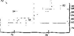
图5表示根据本发明另一个实施方案的半导体结构72。结构72包括单晶半导体衬底74,例如单晶硅晶片,它包括区域75和76。在区域75中利用半导体工业中通常使用的硅器件加工技术来形成由虚线示意性所示的电气元件78。利用与上述类似的步骤,形成单晶氧化物层80和中间无定形氧化硅层82,覆盖衬底74的区域76。形成模板层84和随后的单晶半导体层86,覆盖单晶氧化物层80。根据本发明的再一实施方案,采用与形成层80类似的步骤,形成附加单晶氧化物层88,覆盖层86,并采用与形成层86类似的步骤,形成附加的单晶半导体层90,覆盖单晶氧化物层88。根据本发明的一个实施方案,层86和层90中的至少一个由化合物半导体材料形成。Figure 5 shows a
在单晶半导体层86中至少部分形成由虚线92概括表示的半导体元件。根据本发明的一个实施方案,半导体元件92包括具有部分由单晶氧化物层88形成的栅极介质的场效应晶体管。另外,单晶半导体层92可以用于实施场效应晶体管的门电极。根据本发明的一个实施方案,单晶半导体层86由III-V族化合物形成,并且半导体元件92是射频放大器,它利用了III-V族材料的高迁移率特性。根据本发明的再一个实施方案,由线94示意性表示的电连接使元件78和92相互电连接。因此结构72将利用了两种单晶半导体材料独特性能的元件集成在一起。A semiconductor element generally indicated by a dotted
在图6-18中通过更具体的实施例阐述了其它集成电路和系统。图6的简化方框图说明了具有信号收发部件101、集成电路102、输出单元103以及输入单元104的通讯设备100。信号收发部件的示例包括天线、调制解调器或者用于将信息或数据发送给外部单元或从外部单元发出的其它部件。此处收发一词表示可以与通讯设备之间只接收、只发送或同时接收和发送信号的信号收发部件。输出单元103可以包括显示器、监视器、扬声器等。输入单元可以包括麦克风、键盘等。要注意的是,在该可选实施方案中,输出单元103和输入单元104可以由单个单元例如存储器等来代替。存储器可以包括随机存取存储器或非易失性存储器,例如硬盘、闪存卡或模块等。Other integrated circuits and systems are illustrated by more specific embodiments in FIGS. 6-18. The simplified block diagram of FIG. 6 illustrates a communication device 100 having a signal transceiving unit 101 , an
集成电路通常是不可分离地结合在连续的衬底上或衬底中的至少两个电路元件(例如晶体管、二极管、电阻、电容等)的组合。集成电路102包括一个化合物半导体部分1022、一个双极部分1024以及一个MOS部分1026。化合物半导体部分1022包括至少部分形成在化合物半导体材料中的电气元件。在化合物半导体部分1022中的晶体管和其它电气元件能够在至少约0.8GHz的射频下处理信号。在另一个实施方案中,信号可以处于更低或更高的频率。例如,某些材料例如砷化铟镓,能够在约27GHz的射频处理信号。An integrated circuit is generally a combination of at least two circuit elements (eg transistors, diodes, resistors, capacitors, etc.) inseparably bonded on or in a continuous substrate.
化合物半导体部分1022还包括双工器10222,射频-基带转换器10224(解调部件或解调电路)、基带-射频转换器10226(调制部件或调制电路)、功率放大器10228以及隔离器10229。双极部分1024和MOS部分1026一般由IV族半导体材料形成。双极部分1024包括接收放大器10242、模拟-数字转换器10244、数字-模拟转换器10246以及发送放大器10248。MOS部分1026包括数字信号处理部件10262。这种部件的示例包括任何在市场上可以获得的普通DSP芯,例如数字信号处理器的MotorolaDSP566xx(来自Motorola,Incorporated ofSchaumburg,Illinois)以及德州仪器TMS320C54x(来自德克萨斯Dallas的德州仪器公司)系列。这种数字信号处理部件10262一般包括互补MOS(CMOS)晶体管以及模拟-数字和数字-模拟转换器。显然,在集成电路102中还有其它电气元件。The
在一种工作模式中,通讯设备100接收来自作为信号收发部件101一部分的天线的信号。该信号经过双工器10227被送至射频-基带转换器10224。模拟数据或其它信息被接收放大器10224放大,并被传送给数字信号处理部件10262。在数字信号处理部件10262处理了该信息或其它数据之后,将经过处理的信息或其它数据传送给输出单元103。如果通讯设备是寻呼机,输出单元可以是显示器。如果通讯设备是手持电话,输出单元103可以包括扬声器、显示器或两者都有。In one mode of operation, the communication device 100 receives signals from an antenna that is part of the signal transceiving unit 101 . The signal is sent to the radio frequency-baseband converter 10224 through the duplexer 10227. The analog data or other information is amplified by receive amplifier 10224 and passed to digital signal processing component 10262 . After the digital signal processing section 10262 processes the information or other data, the processed information or other data is transmitted to the output unit 103 . If the communication device is a pager, the output unit may be a display. If the communication device is a handheld phone, the output unit 103 may include a speaker, a display, or both.
数据或其它信息可以通过通讯设备100沿着相反方向传送。数据或其它信息会进入输入单元104。在手持电话中,这会包括麦克风或键盘。然后利用数字信号处理部件10262来处理该信息或其它数据。在处理之后,利用数字-模拟转换器10246转换信号。经过转换的信号被发送放大器10248放大。该被放大的信号由基带-射频转换器10226调制,并进一步由功率放大器10228放大。被放大的RF信号经过隔离器10229和双工器10222到达天线。Data or other information may be communicated in the opposite direction via communication device 100 . Data or other information enters the input unit 104 . In a handheld phone, this would include a microphone or keypad. This information or other data is then processed using digital signal processing components 10262 . After processing, the signal is converted using a digital-to-analog converter 10246 . The converted signal is amplified by the transmit amplifier 10248 . The amplified signal is modulated by the baseband-to-radio frequency converter 10226 and further amplified by the power amplifier 10228. The amplified RF signal passes through the isolator 10229 and the duplexer 10222 to the antenna.
通讯设备100的现有技术的实施方案具有至少两个独立的集成电路:一个用于化合物半导体部分1022,一个用于MOS部分1026。双极部分1024可以在同一个集成电路上例如MOS部分1026上,或也还可以在另一个集成电路上。根据本发明的实施方案,所有这三个部分可以在一个集成电路中形成。因为所有的晶体管可以位于一个集成电路上,所以该通讯设备可以被显著的小型化,并且使得通讯设备具有更大的便携性。A prior art implementation of the communication device 100 has at least two separate integrated circuits: one for the
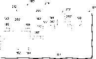
现在描述如图7-11所示的集成电路102示例部分的形成方法。在图7中,p型掺杂的单晶硅衬底110设有化合物半导体部分1022、双极部分1024以及MOS部分1026。在该双极部分中,单晶硅衬底被掺杂以形成N+埋置区1102。然后在埋置区1102和衬底110上形成轻微p型掺杂的外延单晶硅层1104。然后进行掺杂以在埋置区1102上形成轻微n型掺杂的漂移区1117。掺杂步骤将双极区域1024的一部分内的轻微p型掺杂的外延层的掺杂类型转换为轻微n型掺杂的单晶硅区域。然后在双极部分1024和MOS部分1026之间形成场隔离区1106。在MOS部分1026内的外延层1104的一部分上形成栅极介质层1110,然后在栅极介质层1110上形成门电极1112。侧壁隔离件1115沿着门电极1112和栅极介质层1110的竖直侧面形成。Methods of forming example portions of
在漂移区1117中导入p型掺杂剂,以形成活性(active)或本征基极区1114。然后在双极部分1024中形成n型的深集电极区1108,从而使得能够与埋置区1102电连接。进行选择性的n型掺杂以形成N+掺杂区1116以及发射极区1120。N+掺杂区1116在层1104中沿着门电极1112的相邻侧形成,并且是MOS晶体管的源、漏或源/漏区。N+掺杂区1116以及发射极区1120具有的掺杂浓度至少是1E19原子/立方厘米,从而使得能够形成欧姆接触。形成p型掺杂区以形成非活性或非本征基极区1118,该区域是p+掺杂区(掺杂浓度至少是1E19原子/立方厘米)。A p-type dopant is introduced into the
在所述实施方案中,已经进行几个处理步骤,但是不再说明或进一步描述,例如形成阱区、阀值调整掺杂物、防止沟道穿通(channelpunch through)掺杂物、防止场穿通(field punch through)掺杂物、以及各种掩膜层。在该方法中至此的器件形成是采用常规的步骤。如前所述,在MOS区1026内已经形成标准的N沟道MOS晶体管,在双极区1024中已经形成竖直NPN双极晶体管。就这一点而言,在化合物半导体部分1022中没有形成电路。In the described embodiment, several processing steps have been performed but are not illustrated or further described, such as forming well regions, threshold adjusting dopants, preventing channel punch through dopants, preventing field punch through ( field punch through) dopant, and various mask layers. Device formation up to this point in the method follows conventional steps. As previously mentioned, standard N-channel MOS transistors have been formed in
现在,从化合物半导体部分1022的表面除去在集成电路的双极和MOS部分的加工过程中已经形成的所有层。这样就为这个部分的后续处理提供了裸露的硅表面,例如按照上述方式。All layers that have been formed during the processing of the bipolar and MOS portions of the integrated circuit are now removed from the surface of the
然后如图8所示在衬底110上形成调节缓冲层124。调节缓冲层会在在部分1022中适当加工(即具有适当的模板层)的裸露硅表面上形成为单晶层。但是在部分1024和1026之上形成的部分层124可以是多晶的或无定形的,因为它形成在不是单晶的材料上面,因此不会成单晶生长成核。调节缓冲层124通常是单晶金属氧化物或氮化物层,一般的厚度大致为2-100纳米。在一个具体实施方案中,调节缓冲层的厚度大致为5-15纳米。在调节缓冲层形成过程中,沿着集成电路102的最上面的硅表面形成无定形中间层122。该无定形中间层122通常包括有硅的氧化物并且厚度大致为1-5nm。在一个具体的实施方案中,该厚度大致为2nm。在调节缓冲层124和无定形中间层122形成之后,再形成模板层126,它的厚度大致为某种材料的1-10个单层。在一个具体的实施方案中,该材料包括钛-砷、锶-氧-砷、或其它类似的材料,如前参考图1-5所述。An
然后如图9所示外延生长单晶化合物半导体层132,覆盖调节缓冲层124的单晶部分。生长在不是单晶的部分层124上的部分层132可能是多晶的或无定形的。单晶化合物半导体层可以采用多种方法来形成,并且通常包括有例如砷化镓、砷化铝镓、磷化铟或如前所述的其它化合物半导体材料的材料。该层的厚度大致为1-5000nm,更优选为100-500nm。在该具体的实施方案中,模板层中的每种元素也存在于调节缓冲层124、单晶化合物半导体材料132或两者之中。因此模板层126和它的两个相邻层之间的轮廓在加工过程中消失。因此当拍摄透射电子显微镜(TEM)照片时,可以看见调节缓冲层124和单晶化合物半导体层132之间的界面。Then, as shown in FIG. 9 , a single crystal compound semiconductor layer 132 is epitaxially grown to cover the single crystal portion of the
此时,从覆盖双极区1024和MOS区126的部分除去化合物半导体层132和调节缓冲层24的一部分,如图10所示。在该部分除去之后,在衬底110上形成绝缘层142。该绝缘层142可以包括多种材料,例如氧化物、氮化物、氧氮化物、低k介电材料等。此处使用的低k是介电常数不高于大致3.5的材料。在沉积了绝缘层142之后,将其抛光,从而除去覆盖单晶化合物半导体层132的部分绝缘层142。At this time, part of the compound semiconductor layer 132 and the adjustment buffer layer 24 are removed from the portion covering the
然后在单晶化合物半导体部分1022内形成晶体管144。然后在单晶化合物半导体层132上形成门电极148。然后在单晶化合物半导体层132内形成掺杂区146。在这个实施方案中,晶体管144是金属半导体场效应晶体管(MESFET)。如果MESFET是n型MESFET,掺杂区146和单晶化合物半导体层132也是n型掺杂的。如果要形成p型MESFET,那么掺杂区146和单晶化合物半导体层132也具有相反的掺杂类型。较多掺杂(N+)的区146可以与单晶化合物半导体层132形成欧姆接触。此时,集成电路中的有源器件就已经形成。该具体的实施方案包括一个n型MESFET、一个竖直NPN双极晶体管以及一个平面n通道MOS晶体管。可以使用许多其它类型的晶体管,包括P通道MOS晶体管、P型竖直双极晶体管、p型MESFET以及纵向竖直和平面晶体管的结合。而且可以在部分1022、1024和1026中的一个或多个部分中形成其它电气元件,例如电阻、电容、二极管等。Transistor 144 is then formed within single crystal
继续加工以形成基本完成的集成电路102,如图11所示。在衬底110上形成绝缘层152。该绝缘层152可以包括停止蚀刻区(etch-stopregion)和停止抛光区(polish-stop region),这些在图11中没有显示。然后在第一绝缘层152上形成第二绝缘层154。除去部分层154、152、142、124以及122以形成用来使这些器件相互连接的接点开口。在绝缘层154中形成互联沟槽,以提供接触点之间的横向连接。如图11所示,互联1562将部分1022内的n型MESFET的源区或漏区连接至双极部分1024内的NPN晶体管的深集电极区1108。NPN晶体管的发射极区1120连接在MOS部分1026内的n通道MOS晶体管的掺杂区1116之一上。其它掺杂区1116与集成电路没有示出的其它部分电连接。Processing continues to form a substantially completed
在互联件1562、1564和1566以及绝缘层154上形成钝化层156。还有其它电连接到如图所示的晶体管和集成电路102内其它电学和电子元件,但图中未示出。另外,如果需要可以形成附加绝缘层和互联件,以在集成电路102内各种元件之间形成适当的互联。Passivation layer 156 is formed on interconnects 1562 , 1564 and 1566 and insulating layer 154 . There are other electrical connections to transistors and other electrical and electronic components within
从前面的实施方案中可以看出,用于化合物半导体和IV族半导体材料的有源器件可以被集成在一个集成电路中。因为在将双极晶体管和MOS晶体管两者结合进同一个集成电路中存在一些困难,所以可以将双极部分内的一些元件移进化合物半导体部分1022或MOS部分1024中。更具体地说,如图6所示的实施方案,放大器10248和10242可以移到化合物半导体部分1022,转换器10244和10246可以移动到MOS部分1026。因此,可以取消只用于制造双极晶体管的特定制造步骤。因此集成电路只有化合物半导体部分和MOS部分。As can be seen from the previous embodiments, active devices for compound semiconductor and Group IV semiconductor materials can be integrated in one integrated circuit. Because of some difficulties in combining both bipolar and MOS transistors into the same integrated circuit, some elements within the bipolar portion can be moved into either the
在再一个实施方案中,可以形成这样的集成电路,使得它在化合物半导体部分包括光学激光器,并包括连接至同一个集成电路的IV族半导体区内的MOS晶体管的光学互联(波导)。图12-18阐述了一个In yet another embodiment, an integrated circuit may be formed such that it includes an optical laser in the compound semiconductor portion and includes optical interconnects (waveguides) to MOS transistors in the Group IV semiconductor region of the same integrated circuit. Figure 12-18 illustrates a
实施方案。implementation plan.
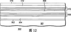
图12是一部分集成电路160的截面图,该集成电路包括单晶硅晶片161。与前文所述类似的无定形中间层162和调节缓冲层164形成在晶片161上。在该具体的实施方案中,首先要形成用于形成光学激光器的层,然后形成用于MOS晶体管的层。在图12中,下反射镜层(mirror layer)166包括化合物半导体材料的交替层。例如光学激光器内的第一、第三和第五层膜可以包括例如砷化镓的材料,而下反射镜层166内的第二、第四和第六层膜可以包括砷化铝镓的材料;或者反之。层168包括用于产生光子的活性区。上反射镜层170以和下反射镜层166类似的方式形成,并且包括化合物半导体材料的交替膜。在一个具体的实施方案中,上反射镜层170可以是p型掺杂的化合物半导体材料,下反射镜层166可以是n型掺杂的化合物半导体材料。FIG. 12 is a cross-sectional view of a portion of an
类似于调节缓冲层164的另一个调节缓冲层172形成在上反射镜层170上。在一个替代实施方案中,调节缓冲层164和172可以包括不同的材料。但是它们的功能基本相同,因为每一个用于在化合物半导体层和单晶IV族半导体层之间形成过渡。单晶IV族半导体层174在调节缓冲层172上形成。在一个具体的实施方案中,单晶IV族半导体层174包括锗、锗化硅(silicon germanium)、硅锗碳化物等。Another
在图13中,MOS部分被加工,以在该上单晶IV族半导体层174中形成电气元件。如图13所示,场隔离区171由一部分层174形成。在层174上形成门介电层173,在门介电层173上形成门电极175。掺杂区是用于晶体管181的源区、漏区或源/漏区,如图所示。与门电极175的竖直侧面相邻形成侧壁隔离件179。可以在至少部分层174中形成其它元件。这些其它元件包括其它的晶体管(n沟道或p沟道)、电容、晶体管、二极管等。In FIG. 13 , the MOS portion is processed to form electrical elements in the upper single crystal group
单晶IV族半导体层在掺杂区177之一上外延生长。上部184是P+掺杂的,下部182仍基本保持为本征的(未掺杂),如图13所示。可以采用选择性外延方法形成该层。在一个实施方案中,在晶体管181和场隔离区171上形成绝缘层(未图示)。将绝缘层形成图案,以限定暴露掺杂区177之一的开口。至少在最初,不用掺杂剂来形成选择性外延层。整个选择性外延层可以是本征的,或可以在选择性外延层的形成接近结束之时加入p型掺杂剂。如果选择性外延层形成时是本征的,则通过注入或通过炉掺杂(furnace doping)来进行掺杂步骤。不管P+上部184是如何形成的,然后除去绝缘层以形成如图13所示的所得到的结构。A single crystal group IV semiconductor layer is epitaxially grown on one of the doped
进行下一系列步骤来形成如图14所示的光学激光器。在集成电路的化合物半导体部分之上除去场隔离区171和调节缓冲层172。进行附加步骤以形成光学激光器180的上反射镜层170和有源层168。上反射镜层170和有源层168的侧面基本是相连的。The next series of steps are performed to form the optical laser as shown in FIG. 14 .
形成接触件186和188,用于分别形成与上反射镜层170和有源层168的电连接,如图14所示。接触件186为环状,以允许光(光子)穿过上反射镜170进入随后形成的光波导内。
然后形成绝缘层190,并使其形成图案,从而形成延伸至接触层和掺杂区177之一的光学开口,如图15所示。绝缘材料可以是任何数量的不同材料,包括氧化物、氮化物、氧氮化物、低k介电材料或它们的任意组合。在形成了开口192之后,在开口内形成折射率较高的材料202,以填充开口,并在绝缘层190之上沉积该层,如图16所示。关于折射率较高的材料202,“较高”是相对于绝缘层190的材料而言(即材料202具有比绝缘层190更高的折射率)。可选的是,可以在形成较高折射率材料202之前形成相对较薄的折射率较低的膜(未示出)。然后在折射率较高的层202上形成硬掩膜层204。从覆盖开口的部分至更靠近图16侧面的区域除去部分硬掩膜层204以及高折射率层202。Insulating
如图17所示,完成作为光互联件的光波导的形成的剩余部分。进行沉积工序(可以是沉积-蚀刻工艺(dep-etch process))以有效地形成侧壁部分212。在该实施方案中,侧壁部分212由与材料202相同的材料形成。然后除去硬掩膜层204,在折射率较高的材料212和202以及绝缘层190的暴露部分上形成低折射率层214(相对于材料202和层212较低)。图17中虚线表示高折射率材料202和212之间的边界。这个标记表示这两个是由同样的材料制成的,但是是在不同的时间形成的。As shown in FIG. 17, the remainder of the formation of the optical waveguide as the optical interconnect is completed. A deposition process (which may be a dep-etch process) is performed to effectively form the
继续进行加工以形成基本完整的集成电路,如图18所示。然后在光学激光器180和MOSFET晶体管181上形成钝化层220。尽管没有显示出,但是其它电学或光学连接可以连接至集成电路中的元件上,但没有在图18中显示出。这些互联件包括其它光波导或可以包括金属互联件。Processing continues to form a substantially complete integrated circuit, as shown in FIG. 18 . Passivation layer 220 is then formed over
在其它的实施方案中,可以形成其它类型的激光器。例如另一种激光器可以水平地而不是竖直地发射光(光子)。如果光线水平地发射出,则可以在衬底161中形成MOSFET晶体管,并且可以重构造光波导,从而使激光器与晶体管适当地连接(光学连接)。在一个具体的实施方案中,光波导可以包括至少一部分调节缓冲层。其它结构也是可以的。In other embodiments, other types of lasers may be formed. For example another laser may emit light (photons) horizontally rather than vertically. If the light is emitted horizontally, a MOSFET transistor can be formed in the
显然这些具有化合物半导体部分和IV族半导体部分的集成电路实施方案是用来解释本发明的实施方案的,而不是对本发明的限制。本发明可以有多种其它的结合和其它的实施方案。例如化合物半导体部分可以包括发光二极管、光电检测器、二极管等,IV族半导体部分可以包括数字逻辑电路、存储器阵列和可以在传统的MOS集成电路中形成的大多数结构。通过采用本发明的实施方案,可以简单地将在化合物半导体材料中工作更好的设备与在IV族半导体材料中工作更好的其它元件集成在一起。这使得设备尺寸缩小,制造成本降低,生产率和可靠性提高。It is apparent that these integrated circuit embodiments having compound semiconductor portions and Group IV semiconductor portions are illustrative of embodiments of the invention, not limitations of the invention. The present invention is capable of various other combinations and other embodiments. For example, compound semiconductor parts may include light emitting diodes, photodetectors, diodes, etc. Group IV semiconductor parts may include digital logic circuits, memory arrays and most structures that can be formed in conventional MOS integrated circuits. By employing embodiments of the present invention, devices that work better in compound semiconductor materials can be easily integrated with other components that work better in Group IV semiconductor materials. This results in reduced device size, reduced manufacturing costs, and improved productivity and reliability.
尽管没有说明,但是单晶IV族晶片可以被用于在晶片之上只形成化合物半导体电子元件。以这种方式,晶片基本是在覆盖晶片的单晶化合物半导体层内制造化合物半导体电子元件过程中使用的“处理(handle)”晶片。因此,电子元件可以在晶片上在III-V或II-VI族半导体材料中形成,直径至少大致是200毫米,可以至少是300毫米。Although not illustrated, a single crystal Group IV wafer may be used to form only compound semiconductor electronic components on the wafer. In this way, the wafer is essentially a "handle" wafer used in the manufacture of compound semiconductor electronic components within the single crystal compound semiconductor layer covering the wafer. Thus, electronic components may be formed on a wafer in a III-V or II-VI semiconductor material with a diameter of at least approximately 200 mm, and may be at least 300 mm.
通过使用这种类型的衬底,通过将化合物半导体晶片放置在相对较耐久并容易制造的基底材料上,相对廉价的“处理(handle)”晶片可以克服化合物半导体晶片的易碎特性。因此可以形成这样的集成电路,使得所有的电气元件、特别是所有的有源电子器件可以在化合物半导体材料中形成,即使该衬底本身可以包括IV族半导体材料。因为与相对较小的、更易碎的传统化合物半导体晶片相比,可以更经济和更容易的加工较大的衬底,所以可以降低化合物半导体设备的制造成本。By using this type of substrate, relatively inexpensive "handle" wafers can overcome the fragile nature of compound semiconductor wafers by placing the compound semiconductor wafers on a relatively durable and easily manufactured base material. It is thus possible to form integrated circuits such that all electrical components, in particular all active electronic devices, are formed in compound semiconductor materials, even though the substrate itself may comprise group IV semiconductor materials. Compound semiconductor device manufacturing costs can be reduced because larger substrates can be more economically and easily processed compared to relatively smaller, more fragile conventional compound semiconductor wafers.
在前述说明书中,本发明已经参考特定实施方案进行了说明。但是该领域的技术人员可以理解的是,在不脱离如权利要求所限定的本发明的范围的情况下可以作出各种改进和变化。因此说明书和附图被认为是用于说明的,而不是进行限制,所有这些改进应包括在本发明的范围内。In the foregoing specification, the invention has been described with reference to specific embodiments. However, it will be appreciated by those skilled in the art that various modifications and changes can be made without departing from the scope of the present invention as defined in the claims. The specification and drawings are therefore to be regarded as illustrative rather than restrictive and all such modifications are intended to be included within the scope of this invention.
上面已结合了具体实施例说明了本发明的好处、其它优点和解决问题的方案。但是,这些好处、优点、解决问题的方案以及可能引起任何好处、优点或解决方案或使之变得更加显著的任何要素都不能成为任何或全部权利要求的关键、必需或基本的特征或要素。此处使用的“包括”、“含有”或它们的任何其它形式的用语是指非排它性的包含,从而,包括一组要素的过程、方法、物品或设备不仅包括这些要素,而是可以包括没有明确列出的或这些过程、方法、物品或设备固有的其它要素。The benefits, other advantages and solutions to the problems of the present invention have been described above in conjunction with specific embodiments. However, none of these benefits, advantages, solutions to problems, and any element that might give rise to or make more pronounced any benefit, advantage, or solution, should be a key, required, or essential feature or element of any or all claims. As used herein, the terms "comprising", "comprising", or any other form thereof mean a non-exclusive inclusion whereby a process, method, article, or apparatus that includes a set of elements not only includes those elements, but may Including other elements not expressly listed or inherent in these processes, methods, articles or equipment.
Claims (15)
Applications Claiming Priority (2)
| Application Number | Priority Date | Filing Date | Title |
|---|---|---|---|
| US09/502,023US6392257B1 (en) | 2000-02-10 | 2000-02-10 | Semiconductor structure, semiconductor device, communicating device, integrated circuit, and process for fabricating the same |
| US09/502,023 | 2000-02-10 |
Publications (2)
| Publication Number | Publication Date |
|---|---|
| CN1398429Atrue CN1398429A (en) | 2003-02-19 |
| CN1222032C CN1222032C (en) | 2005-10-05 |
Family
ID=23995993
Family Applications (5)
| Application Number | Title | Priority Date | Filing Date |
|---|---|---|---|
| CN01804762APendingCN1398423A (en) | 2000-02-10 | 2001-02-08 | Process for forming semiconductor structure |
| CNB01804753XAExpired - Fee RelatedCN1261978C (en) | 2000-02-10 | 2001-02-08 | Semiconductor structure |
| CNB01804798XAExpired - Fee RelatedCN1222032C (en) | 2000-02-10 | 2001-02-08 | communication device |
| CN01804746APendingCN1416590A (en) | 2000-02-10 | 2001-02-08 | Semiconductor structure |
| CN01804799APendingCN1398430A (en) | 2000-02-10 | 2001-02-08 | Semiconductor devices |
Family Applications Before (2)
| Application Number | Title | Priority Date | Filing Date |
|---|---|---|---|
| CN01804762APendingCN1398423A (en) | 2000-02-10 | 2001-02-08 | Process for forming semiconductor structure |
| CNB01804753XAExpired - Fee RelatedCN1261978C (en) | 2000-02-10 | 2001-02-08 | Semiconductor structure |
Family Applications After (2)
| Application Number | Title | Priority Date | Filing Date |
|---|---|---|---|
| CN01804746APendingCN1416590A (en) | 2000-02-10 | 2001-02-08 | Semiconductor structure |
| CN01804799APendingCN1398430A (en) | 2000-02-10 | 2001-02-08 | Semiconductor devices |
Country Status (9)
| Country | Link |
|---|---|
| US (9) | US6392257B1 (en) |
| EP (5) | EP1258030A1 (en) |
| JP (5) | JP2003523084A (en) |
| KR (5) | KR100695662B1 (en) |
| CN (5) | CN1398423A (en) |
| AU (7) | AU2001234999A1 (en) |
| CA (2) | CA2399394A1 (en) |
| TW (6) | TW487969B (en) |
| WO (7) | WO2001059835A1 (en) |
Cited By (1)
| Publication number | Priority date | Publication date | Assignee | Title |
|---|---|---|---|---|
| CN116364825A (en)* | 2023-06-01 | 2023-06-30 | 江西兆驰半导体有限公司 | Composite buffer layer, preparation method thereof, epitaxial wafer and light-emitting diode |
Families Citing this family (158)
| Publication number | Priority date | Publication date | Assignee | Title |
|---|---|---|---|---|
| DE19942692B4 (en)* | 1999-09-07 | 2007-04-12 | Infineon Technologies Ag | Optoelectronic microelectronic assembly |
| US6392257B1 (en) | 2000-02-10 | 2002-05-21 | Motorola Inc. | Semiconductor structure, semiconductor device, communicating device, integrated circuit, and process for fabricating the same |
| US6693033B2 (en)* | 2000-02-10 | 2004-02-17 | Motorola, Inc. | Method of removing an amorphous oxide from a monocrystalline surface |
| JP2004503920A (en) | 2000-05-31 | 2004-02-05 | モトローラ・インコーポレイテッド | Semiconductor device and method of manufacturing the semiconductor device |
| US20020030246A1 (en)* | 2000-06-28 | 2002-03-14 | Motorola, Inc. | Structure and method for fabricating semiconductor structures and devices not lattice matched to the substrate |
| AU2001264987A1 (en)* | 2000-06-30 | 2002-01-14 | Motorola, Inc., A Corporation Of The State Of Delware | Hybrid semiconductor structure and device |
| WO2002009187A2 (en) | 2000-07-24 | 2002-01-31 | Motorola, Inc. | Heterojunction tunneling diodes and process for fabricating same |
| US6555946B1 (en) | 2000-07-24 | 2003-04-29 | Motorola, Inc. | Acoustic wave device and process for forming the same |
| US6590236B1 (en)* | 2000-07-24 | 2003-07-08 | Motorola, Inc. | Semiconductor structure for use with high-frequency signals |
| WO2002009148A2 (en)* | 2000-07-24 | 2002-01-31 | Motorola, Inc. | Integrated radiation emitting system and process for fabricating same |
| DE60124766T2 (en)* | 2000-08-04 | 2007-10-11 | Amberwave Systems Corp. | SILICON WAIST WITH MONOLITHIC OPTOELECTRONIC COMPONENTS |
| US7273657B2 (en)* | 2000-08-08 | 2007-09-25 | Translucent Photonics, Inc. | Rare earth-oxides, rare earth-nitrides, rare earth-phosphides and ternary alloys with silicon |
| US6638838B1 (en) | 2000-10-02 | 2003-10-28 | Motorola, Inc. | Semiconductor structure including a partially annealed layer and method of forming the same |
| WO2002033385A2 (en)* | 2000-10-19 | 2002-04-25 | Motorola, Inc. | Biochip excitation and analysis structure |
| US7065124B2 (en)* | 2000-11-28 | 2006-06-20 | Finlsar Corporation | Electron affinity engineered VCSELs |
| US6905900B1 (en) | 2000-11-28 | 2005-06-14 | Finisar Corporation | Versatile method and system for single mode VCSELs |
| US6563118B2 (en)* | 2000-12-08 | 2003-05-13 | Motorola, Inc. | Pyroelectric device on a monocrystalline semiconductor substrate and process for fabricating same |
| US20020096683A1 (en) | 2001-01-19 | 2002-07-25 | Motorola, Inc. | Structure and method for fabricating GaN devices utilizing the formation of a compliant substrate |
| US6589335B2 (en)* | 2001-02-08 | 2003-07-08 | Amberwave Systems Corporation | Relaxed InxGa1-xAs layers integrated with Si |
| US6673646B2 (en) | 2001-02-28 | 2004-01-06 | Motorola, Inc. | Growth of compound semiconductor structures on patterned oxide films and process for fabricating same |
| US20020140012A1 (en)* | 2001-03-30 | 2002-10-03 | Motorola, Inc. | Semiconductor structures and devices for detecting far-infrared light and methods for fabricating same |
| WO2002082551A1 (en) | 2001-04-02 | 2002-10-17 | Motorola, Inc. | A semiconductor structure exhibiting reduced leakage current |
| US6594409B2 (en)* | 2001-04-18 | 2003-07-15 | Apic Corporation | WDM transmitter or receiver including an array waveguide grating and active optical elements |
| US20020163010A1 (en)* | 2001-05-04 | 2002-11-07 | Motorola, Inc. | Wide bandgap semiconductor structure, semiconductor device including the structure, and methods of forming the structure and device |
| US20020175347A1 (en)* | 2001-05-22 | 2002-11-28 | Motorola, Inc. | Hybrid semiconductor input/output structure |
| US20020179957A1 (en)* | 2001-05-29 | 2002-12-05 | Motorola, Inc. | Structure and method for fabricating high Q varactor diodes |
| US20020182762A1 (en)* | 2001-05-30 | 2002-12-05 | Motorola Inc. | Direct conversion/sampling at antenna |
| US20020181827A1 (en)* | 2001-06-01 | 2002-12-05 | Motorola, Inc. | Optically-communicating integrated circuits |
| US7037862B2 (en)* | 2001-06-13 | 2006-05-02 | Micron Technology, Inc. | Dielectric layer forming method and devices formed therewith |
| US20020195599A1 (en)* | 2001-06-20 | 2002-12-26 | Motorola, Inc. | Low-defect semiconductor structure, device including the structure and method for fabricating structure and device |
| US6709989B2 (en) | 2001-06-21 | 2004-03-23 | Motorola, Inc. | Method for fabricating a semiconductor structure including a metal oxide interface with silicon |
| US20030012965A1 (en)* | 2001-07-10 | 2003-01-16 | Motorola, Inc. | Structure and method for fabricating semiconductor structures and devices utilizing the formation of a compliant substrate comprising an oxygen-doped compound semiconductor layer |
| US6992321B2 (en)* | 2001-07-13 | 2006-01-31 | Motorola, Inc. | Structure and method for fabricating semiconductor structures and devices utilizing piezoelectric materials |
| US20030013219A1 (en)* | 2001-07-13 | 2003-01-16 | Motorola, Inc. | Structure and method for fabricating semiconductor structures and devices utilizing electro-optic structures |
| US20030015767A1 (en)* | 2001-07-17 | 2003-01-23 | Motorola, Inc. | Structure and method for fabricating semiconductor structures and devices with integrated control components |
| US20030015134A1 (en)* | 2001-07-18 | 2003-01-23 | Motorola, Inc. | Semiconductor structure for edge mounting applications and process for fabrication |
| US6646293B2 (en) | 2001-07-18 | 2003-11-11 | Motorola, Inc. | Structure for fabricating high electron mobility transistors utilizing the formation of complaint substrates |
| US6693298B2 (en) | 2001-07-20 | 2004-02-17 | Motorola, Inc. | Structure and method for fabricating epitaxial semiconductor on insulator (SOI) structures and devices utilizing the formation of a compliant substrate for materials used to form same |
| US7019332B2 (en) | 2001-07-20 | 2006-03-28 | Freescale Semiconductor, Inc. | Fabrication of a wavelength locker within a semiconductor structure |
| US6855992B2 (en) | 2001-07-24 | 2005-02-15 | Motorola Inc. | Structure and method for fabricating configurable transistor devices utilizing the formation of a compliant substrate for materials used to form the same |
| US20030020144A1 (en)* | 2001-07-24 | 2003-01-30 | Motorola, Inc. | Integrated communications apparatus and method |
| US20030021538A1 (en)* | 2001-07-25 | 2003-01-30 | Motorola, Inc. | Structure and method for fabricating semiconductor structures and devices utilizing optical waveguides |
| US20030020071A1 (en)* | 2001-07-25 | 2003-01-30 | Motorola, Inc. | Integral semiconductor apparatus for conducting a plurality of functions |
| US20030020090A1 (en)* | 2001-07-25 | 2003-01-30 | Motorola, Inc. | Structure including both compound semiconductor devices and silicon devices for optimal performance and function and method for fabricating the structure |
| US6667196B2 (en) | 2001-07-25 | 2003-12-23 | Motorola, Inc. | Method for real-time monitoring and controlling perovskite oxide film growth and semiconductor structure formed using the method |
| US6639249B2 (en) | 2001-08-06 | 2003-10-28 | Motorola, Inc. | Structure and method for fabrication for a solid-state lighting device |
| US6589856B2 (en) | 2001-08-06 | 2003-07-08 | Motorola, Inc. | Method and apparatus for controlling anti-phase domains in semiconductor structures and devices |
| US20030034491A1 (en)* | 2001-08-14 | 2003-02-20 | Motorola, Inc. | Structure and method for fabricating semiconductor structures and devices for detecting an object |
| US6673667B2 (en) | 2001-08-15 | 2004-01-06 | Motorola, Inc. | Method for manufacturing a substantially integral monolithic apparatus including a plurality of semiconductor materials |
| US8026161B2 (en) | 2001-08-30 | 2011-09-27 | Micron Technology, Inc. | Highly reliable amorphous high-K gate oxide ZrO2 |
| JP4543162B2 (en)* | 2001-09-05 | 2010-09-15 | 独立行政法人産業技術総合研究所 | ZnOSSe mixed crystal semiconductor |
| DE10197029D2 (en) | 2001-10-15 | 2004-10-28 | Infineon Technologies Ag | Laser diode unit and arrangement for operating a laser diode |
| US20030071327A1 (en)* | 2001-10-17 | 2003-04-17 | Motorola, Inc. | Method and apparatus utilizing monocrystalline insulator |
| US6737339B2 (en)* | 2001-10-24 | 2004-05-18 | Agere Systems Inc. | Semiconductor device having a doped lattice matching layer and a method of manufacture therefor |
| WO2003038878A2 (en)* | 2001-10-26 | 2003-05-08 | Motorola Inc. | Method for fabricating semiconductor structures |
| US6893984B2 (en)* | 2002-02-20 | 2005-05-17 | Micron Technology Inc. | Evaporated LaA1O3 films for gate dielectrics |
| US6872252B2 (en)* | 2002-03-06 | 2005-03-29 | Agilent Technologies, Inc. | Lead-based perovskite buffer for forming indium phosphide on silicon |
| US6815248B2 (en)* | 2002-04-18 | 2004-11-09 | Infineon Technologies Ag | Material combinations for tunnel junction cap layer, tunnel junction hard mask and tunnel junction stack seed layer in MRAM processing |
| US7589029B2 (en) | 2002-05-02 | 2009-09-15 | Micron Technology, Inc. | Atomic layer deposition and conversion |
| US7160577B2 (en) | 2002-05-02 | 2007-01-09 | Micron Technology, Inc. | Methods for atomic-layer deposition of aluminum oxides in integrated circuits |
| EP1359614A1 (en)* | 2002-05-02 | 2003-11-05 | Agilent Technologies, Inc. - a Delaware corporation - | Semiconductor substrates and structures with an oxide layer |
| US6916717B2 (en) | 2002-05-03 | 2005-07-12 | Motorola, Inc. | Method for growing a monocrystalline oxide layer and for fabricating a semiconductor device on a monocrystalline substrate |
| US7135421B2 (en) | 2002-06-05 | 2006-11-14 | Micron Technology, Inc. | Atomic layer-deposited hafnium aluminum oxide |
| US6884739B2 (en)* | 2002-08-15 | 2005-04-26 | Micron Technology Inc. | Lanthanide doped TiOx dielectric films by plasma oxidation |
| US7608927B2 (en)* | 2002-08-29 | 2009-10-27 | Micron Technology, Inc. | Localized biasing for silicon on insulator structures |
| US6965626B2 (en)* | 2002-09-03 | 2005-11-15 | Finisar Corporation | Single mode VCSEL |
| US6791125B2 (en)* | 2002-09-30 | 2004-09-14 | Freescale Semiconductor, Inc. | Semiconductor device structures which utilize metal sulfides |
| JP2004158717A (en)* | 2002-11-07 | 2004-06-03 | Fujitsu Ltd | Thin film laminate, electronic device and actuator using the thin film laminate, and method of manufacturing actuator |
| US7169619B2 (en) | 2002-11-19 | 2007-01-30 | Freescale Semiconductor, Inc. | Method for fabricating semiconductor structures on vicinal substrates using a low temperature, low pressure, alkaline earth metal-rich process |
| US6885065B2 (en) | 2002-11-20 | 2005-04-26 | Freescale Semiconductor, Inc. | Ferromagnetic semiconductor structure and method for forming the same |
| US6813293B2 (en)* | 2002-11-21 | 2004-11-02 | Finisar Corporation | Long wavelength VCSEL with tunnel junction, and implant |
| US6806202B2 (en) | 2002-12-03 | 2004-10-19 | Motorola, Inc. | Method of removing silicon oxide from a surface of a substrate |
| US6770504B2 (en)* | 2003-01-06 | 2004-08-03 | Honeywell International Inc. | Methods and structure for improving wafer bow control |
| US7020374B2 (en) | 2003-02-03 | 2006-03-28 | Freescale Semiconductor, Inc. | Optical waveguide structure and method for fabricating the same |
| US6965128B2 (en) | 2003-02-03 | 2005-11-15 | Freescale Semiconductor, Inc. | Structure and method for fabricating semiconductor microresonator devices |
| US6890816B2 (en)* | 2003-02-07 | 2005-05-10 | Freescale Semiconductor, Inc. | Compound semiconductor structure including an epitaxial perovskite layer and method for fabricating semiconductor structures and devices |
| US7026690B2 (en)* | 2003-02-12 | 2006-04-11 | Micron Technology, Inc. | Memory devices and electronic systems comprising integrated bipolar and FET devices |
| JP2004273562A (en)* | 2003-03-05 | 2004-09-30 | Seiko Epson Corp | Light emitting device and manufacturing method thereof |
| US7135369B2 (en) | 2003-03-31 | 2006-11-14 | Micron Technology, Inc. | Atomic layer deposited ZrAlxOy dielectric layers including Zr4AlO9 |
| US7183186B2 (en) | 2003-04-22 | 2007-02-27 | Micro Technology, Inc. | Atomic layer deposited ZrTiO4 films |
| US20040222363A1 (en)* | 2003-05-07 | 2004-11-11 | Honeywell International Inc. | Connectorized optical component misalignment detection system |
| US20040247250A1 (en)* | 2003-06-03 | 2004-12-09 | Honeywell International Inc. | Integrated sleeve pluggable package |
| US8889530B2 (en)* | 2003-06-03 | 2014-11-18 | The Research Foundation Of State University Of New York | Formation of highly dislocation free compound semiconductor on a lattice mismatched substrate |
| WO2004109775A2 (en)* | 2003-06-03 | 2004-12-16 | The Research Foundation Of State University Of New York | Formation of highly dislocation free compound semiconductor on a lattice mismatched substrate |
| US7298942B2 (en) | 2003-06-06 | 2007-11-20 | Finisar Corporation | Pluggable optical optic system having a lens fiber stop |
| JP4663216B2 (en)* | 2003-06-10 | 2011-04-06 | ルネサスエレクトロニクス株式会社 | Semiconductor memory device and manufacturing method thereof |
| US7433381B2 (en) | 2003-06-25 | 2008-10-07 | Finisar Corporation | InP based long wavelength VCSEL |
| US7277461B2 (en)* | 2003-06-27 | 2007-10-02 | Finisar Corporation | Dielectric VCSEL gain guide |
| US7075962B2 (en)* | 2003-06-27 | 2006-07-11 | Finisar Corporation | VCSEL having thermal management |
| US7054345B2 (en) | 2003-06-27 | 2006-05-30 | Finisar Corporation | Enhanced lateral oxidation |
| US7149383B2 (en)* | 2003-06-30 | 2006-12-12 | Finisar Corporation | Optical system with reduced back reflection |
| US6961489B2 (en) | 2003-06-30 | 2005-11-01 | Finisar Corporation | High speed optical system |
| US20060056762A1 (en)* | 2003-07-02 | 2006-03-16 | Honeywell International Inc. | Lens optical coupler |
| US7210857B2 (en)* | 2003-07-16 | 2007-05-01 | Finisar Corporation | Optical coupling system |
| US20050013539A1 (en)* | 2003-07-17 | 2005-01-20 | Honeywell International Inc. | Optical coupling system |
| JP4689153B2 (en)* | 2003-07-18 | 2011-05-25 | 株式会社リコー | Laminated substrate and semiconductor device |
| US6887801B2 (en)* | 2003-07-18 | 2005-05-03 | Finisar Corporation | Edge bead control method and apparatus |
| US7031363B2 (en)* | 2003-10-29 | 2006-04-18 | Finisar Corporation | Long wavelength VCSEL device processing |
| US7135753B2 (en) | 2003-12-05 | 2006-11-14 | International Rectifier Corporation | Structure and method for III-nitride monolithic power IC |
| GB0405325D0 (en)* | 2004-03-10 | 2004-04-21 | Koninkl Philips Electronics Nv | Trench-gate transistors and their manufacture |
| JP4874527B2 (en)* | 2004-04-01 | 2012-02-15 | トヨタ自動車株式会社 | Silicon carbide semiconductor substrate and method for manufacturing the same |
| CN100492668C (en)* | 2004-05-25 | 2009-05-27 | 中国科学院福建物质结构研究所 | A range of semiconductor materials |
| CN100485867C (en)* | 2004-07-20 | 2009-05-06 | 中国科学院物理研究所 | Epitaxial growth of lanthanum aluminate film material on silicon substrate and preparation method |
| US7601649B2 (en) | 2004-08-02 | 2009-10-13 | Micron Technology, Inc. | Zirconium-doped tantalum oxide films |
| US7081421B2 (en) | 2004-08-26 | 2006-07-25 | Micron Technology, Inc. | Lanthanide oxide dielectric layer |
| US7588988B2 (en) | 2004-08-31 | 2009-09-15 | Micron Technology, Inc. | Method of forming apparatus having oxide films formed using atomic layer deposition |
| US7494939B2 (en) | 2004-08-31 | 2009-02-24 | Micron Technology, Inc. | Methods for forming a lanthanum-metal oxide dielectric layer |
| US7309660B2 (en)* | 2004-09-16 | 2007-12-18 | International Business Machines Corporation | Buffer layer for selective SiGe growth for uniform nucleation |
| US7560395B2 (en) | 2005-01-05 | 2009-07-14 | Micron Technology, Inc. | Atomic layer deposited hafnium tantalum oxide dielectrics |
| US7217643B2 (en)* | 2005-02-24 | 2007-05-15 | Freescale Semiconductors, Inc. | Semiconductor structures and methods for fabricating semiconductor structures comprising high dielectric constant stacked structures |
| US7687409B2 (en) | 2005-03-29 | 2010-03-30 | Micron Technology, Inc. | Atomic layer deposited titanium silicon oxide films |
| JP4876418B2 (en)* | 2005-03-29 | 2012-02-15 | 富士電機株式会社 | Semiconductor device |
| US7390756B2 (en)* | 2005-04-28 | 2008-06-24 | Micron Technology, Inc. | Atomic layer deposited zirconium silicon oxide films |
| US7662729B2 (en) | 2005-04-28 | 2010-02-16 | Micron Technology, Inc. | Atomic layer deposition of a ruthenium layer to a lanthanide oxide dielectric layer |
| US7572695B2 (en) | 2005-05-27 | 2009-08-11 | Micron Technology, Inc. | Hafnium titanium oxide films |
| US7927948B2 (en) | 2005-07-20 | 2011-04-19 | Micron Technology, Inc. | Devices with nanocrystals and methods of formation |
| US7575978B2 (en) | 2005-08-04 | 2009-08-18 | Micron Technology, Inc. | Method for making conductive nanoparticle charge storage element |
| US7989290B2 (en) | 2005-08-04 | 2011-08-02 | Micron Technology, Inc. | Methods for forming rhodium-based charge traps and apparatus including rhodium-based charge traps |
| US20070044832A1 (en)* | 2005-08-25 | 2007-03-01 | Fritzemeier Leslie G | Photovoltaic template |
| US7410910B2 (en) | 2005-08-31 | 2008-08-12 | Micron Technology, Inc. | Lanthanum aluminum oxynitride dielectric films |
| KR101316947B1 (en)* | 2005-11-01 | 2013-10-15 | 메사추세츠 인스티튜트 오브 테크놀로지 | Monolithically integrated semiconductor materials and devices |
| US7410859B1 (en)* | 2005-11-07 | 2008-08-12 | Advanced Micro Devices, Inc. | Stressed MOS device and method for its fabrication |
| US7700423B2 (en)* | 2006-07-28 | 2010-04-20 | Iqe Rf, Llc | Process for manufacturing epitaxial wafers for integrated devices on a common compound semiconductor III-V wafer |
| US7588951B2 (en)* | 2006-11-17 | 2009-09-15 | Freescale Semiconductor, Inc. | Method of packaging a semiconductor device and a prefabricated connector |
| US7807511B2 (en)* | 2006-11-17 | 2010-10-05 | Freescale Semiconductor, Inc. | Method of packaging a device having a multi-contact elastomer connector contact area and device thereof |
| US20080119004A1 (en)* | 2006-11-17 | 2008-05-22 | Burch Kenneth R | Method of packaging a device having a keypad switch point |
| US7696016B2 (en)* | 2006-11-17 | 2010-04-13 | Freescale Semiconductor, Inc. | Method of packaging a device having a tangible element and device thereof |
| US8927392B2 (en)* | 2007-11-02 | 2015-01-06 | Siva Power, Inc. | Methods for forming crystalline thin-film photovoltaic structures |
| US20090261346A1 (en)* | 2008-04-16 | 2009-10-22 | Ding-Yuan Chen | Integrating CMOS and Optical Devices on a Same Chip |
| US8236603B1 (en) | 2008-09-04 | 2012-08-07 | Solexant Corp. | Polycrystalline semiconductor layers and methods for forming the same |
| US8093559B1 (en)* | 2008-12-02 | 2012-01-10 | Hrl Laboratories, Llc | Methods and apparatus for three-color infrared sensors |
| WO2010088366A1 (en)* | 2009-01-28 | 2010-08-05 | Wakonda Technologies, Inc. | Large-grain crystalline thin-film structures and devices and methods for forming the same |
| CN101840971B (en)* | 2009-03-17 | 2012-09-05 | 展晶科技(深圳)有限公司 | Light-emitting diode and manufacturing method thereof |
| US8897470B2 (en) | 2009-07-31 | 2014-11-25 | Macronix International Co., Ltd. | Method of fabricating integrated semiconductor device with MOS, NPN BJT, LDMOS, pre-amplifier and MEMS unit |
| KR102462043B1 (en) | 2009-10-16 | 2022-11-03 | 가부시키가이샤 한도오따이 에네루기 켄큐쇼 | Semiconductor device |
| DE102009051521B4 (en)* | 2009-10-31 | 2012-04-26 | X-Fab Semiconductor Foundries Ag | Production of silicon semiconductor wafers with III-V layer structures for high electron mobility transistors (HEMT) and a corresponding semiconductor layer arrangement |
| US9012253B2 (en) | 2009-12-16 | 2015-04-21 | Micron Technology, Inc. | Gallium nitride wafer substrate for solid state lighting devices, and associated systems and methods |
| US8680510B2 (en) | 2010-06-28 | 2014-03-25 | International Business Machines Corporation | Method of forming compound semiconductor |
| US8164092B2 (en)* | 2010-10-18 | 2012-04-24 | The University Of Utah Research Foundation | PIN structures including intrinsic gallium arsenide, devices incorporating the same, and related methods |
| US20120126239A1 (en)* | 2010-11-24 | 2012-05-24 | Transphorm Inc. | Layer structures for controlling stress of heteroepitaxially grown iii-nitride layers |
| US9312436B2 (en) | 2011-05-16 | 2016-04-12 | Kabushiki Kaisha Toshiba | Nitride semiconductor device, nitride semiconductor wafer, and method for manufacturing nitride semiconductor layer |
| US9879357B2 (en) | 2013-03-11 | 2018-01-30 | Tivra Corporation | Methods and systems for thin film deposition processes |
| EP2862206A4 (en)* | 2012-06-14 | 2015-12-30 | Tivra Corp | Multilayer substrate structure and method and system of manufacturing the same |
| JP6107435B2 (en)* | 2013-06-04 | 2017-04-05 | 三菱電機株式会社 | Semiconductor device and manufacturing method thereof |
| KR102171268B1 (en) | 2014-09-30 | 2020-11-06 | 삼성전자 주식회사 | manufacturing method of Hybrid silicon laser |
| JP6956716B2 (en)* | 2015-11-13 | 2021-11-02 | アイキューイー ピーエルシーIQE plc | Layer structure for RF filters processed with rare earth oxides and epitaxial aluminum nitride |
| CN105428384B (en)* | 2015-12-28 | 2018-08-10 | 上海集成电路研发中心有限公司 | A kind of image sensor and its manufacturing method |
| WO2018004693A1 (en)* | 2016-07-01 | 2018-01-04 | Intel Corporation | Substrates for integrated circuits |
| US11495670B2 (en) | 2016-09-22 | 2022-11-08 | Iqe Plc | Integrated epitaxial metal electrodes |
| US10553494B2 (en)* | 2016-11-29 | 2020-02-04 | Taiwan Semiconductor Manufacturing Company, Ltd. | Breakdown resistant semiconductor apparatus and method of making same |
| US10083963B2 (en)* | 2016-12-21 | 2018-09-25 | Qualcomm Incorporated | Logic circuit block layouts with dual-side processing |
| EP3568873B1 (en)* | 2017-01-13 | 2023-11-08 | Massachusetts Institute of Technology | A method of forming a multilayer structure for a pixelated display and a multilayer structure for a pixelated display |
| GB2565054A (en)* | 2017-07-28 | 2019-02-06 | Comptek Solutions Oy | Heterostructure semiconductor device and manufacturing method |
| US10373936B2 (en) | 2017-08-22 | 2019-08-06 | Facebook Technologies, Llc | Pixel elements including light emitters of variable heights |
| FR3079534B1 (en)* | 2018-03-28 | 2022-03-18 | Soitec Silicon On Insulator | METHOD FOR MANUFACTURING A MONOCRYSTALLINE LAYER OF GAAS MATERIAL AND SUBSTRATE FOR GROWTH BY EPITAXIS OF A MONOCRYSTALLINE LAYER OF GAAS MATERIAL |
| FR3090013B1 (en)* | 2018-12-17 | 2020-12-25 | Commissariat A L Energie Atomique Et Aux Energies Alternatives | PROCESS FOR MANUFACTURING A MONOCRISTALLINE STRUCTURE |
| CN110600362B (en)* | 2019-08-01 | 2022-05-20 | 中国科学院微电子研究所 | Silicon-based heterogeneous integrated material, preparation method thereof and semiconductor device |
| TWI803219B (en) | 2021-03-03 | 2023-05-21 | 美商安托梅拉公司 | Radio frequency (rf) semiconductor devices including a ground plane layer having a superlattice and associated methods |
Family Cites Families (726)
| Publication number | Priority date | Publication date | Assignee | Title |
|---|---|---|---|---|
| US247722A (en)* | 1881-09-27 | John westinghotjse | ||
| US1037272A (en)* | 1907-11-16 | 1912-09-03 | William Godson Lindsay | Bottle. |
| US2152315A (en)* | 1936-12-07 | 1939-03-28 | Kohn Samuel | Frankfurter cooker |
| US3046384A (en)* | 1960-05-04 | 1962-07-24 | Taylor Winfield Corp | Flash welding and trimming apparatus |
| US3617951A (en) | 1968-11-21 | 1971-11-02 | Western Microwave Lab Inc | Broadband circulator or isolator of the strip line or microstrip type |
| US3670213A (en) | 1969-05-24 | 1972-06-13 | Tokyo Shibaura Electric Co | Semiconductor photosensitive device with a rare earth oxide compound forming a rectifying junction |
| US4404265A (en) | 1969-10-01 | 1983-09-13 | Rockwell International Corporation | Epitaxial composite and method of making |
| GB1319311A (en) | 1970-06-04 | 1973-06-06 | North American Rockwell | Epitaxial composite and method of making |
| US3766370A (en) | 1971-05-14 | 1973-10-16 | Hewlett Packard Co | Elementary floating point cordic function processor and shifter |
| US3802967A (en) | 1971-08-27 | 1974-04-09 | Rca Corp | Iii-v compound on insulating substrate and its preparation and use |
| US3914137A (en) | 1971-10-06 | 1975-10-21 | Motorola Inc | Method of manufacturing a light coupled monolithic circuit by selective epitaxial deposition |
| US3758199A (en)* | 1971-11-22 | 1973-09-11 | Sperry Rand Corp | Piezoelectrically actuated light deflector |
| US3818451A (en)* | 1972-03-15 | 1974-06-18 | Motorola Inc | Light-emitting and light-receiving logic array |
| US4006989A (en)* | 1972-10-02 | 1977-02-08 | Raytheon Company | Laser gyroscope |
| US3935031A (en)* | 1973-05-07 | 1976-01-27 | New England Institute, Inc. | Photovoltaic cell with enhanced power output |
| US4084130A (en) | 1974-01-18 | 1978-04-11 | Texas Instruments Incorporated | Laser for integrated optical circuits |
| JPS528835A (en) | 1975-07-11 | 1977-01-24 | Fujitsu Ltd | Connector for fiber optics |
| JPS52135684U (en) | 1975-10-22 | 1977-10-15 | ||
| JPS5816335B2 (en)* | 1976-01-20 | 1983-03-30 | 松下電器産業株式会社 | semiconductor equipment |
| JPS604962B2 (en)* | 1976-01-20 | 1985-02-07 | 松下電器産業株式会社 | optical waveguide device |
| US4120588A (en) | 1976-07-12 | 1978-10-17 | Erik Chaum | Multiple path configuration for a laser interferometer |
| JPS5413455A (en) | 1977-07-01 | 1979-01-31 | Hitachi Ltd | Uniformly expanding device for tube |
| NL7710164A (en) | 1977-09-16 | 1979-03-20 | Philips Nv | METHOD OF TREATING A SINGLE CRYSTAL LINE BODY. |
| US4174422A (en) | 1977-12-30 | 1979-11-13 | International Business Machines Corporation | Growing epitaxial films when the misfit between film and substrate is large |
| US4284329A (en) | 1978-01-03 | 1981-08-18 | Raytheon Company | Laser gyroscope system |
| US4146297A (en)* | 1978-01-16 | 1979-03-27 | Bell Telephone Laboratories, Incorporated | Tunable optical waveguide directional coupler filter |
| US4174504A (en)* | 1978-01-25 | 1979-11-13 | United Technologies Corporation | Apparatus and method for cavity dumping a Q-switched laser |
| JPS54134554U (en) | 1978-03-10 | 1979-09-18 | ||
| JPS5944004B2 (en) | 1978-05-12 | 1984-10-26 | 井関農機株式会社 | Root digging device using vibrating subsoiler |
| JPS558742A (en) | 1978-06-30 | 1980-01-22 | Matsushita Electric Works Ltd | Waterproof facial beauty instrument |
| US4242595A (en) | 1978-07-27 | 1980-12-30 | University Of Southern California | Tunnel diode load for ultra-fast low power switching circuits |
| JPS5587424U (en) | 1978-12-13 | 1980-06-17 | ||
| JPS6136981Y2 (en) | 1979-03-13 | 1986-10-27 | ||
| US4297656A (en) | 1979-03-23 | 1981-10-27 | Harris Corporation | Plural frequency oscillator employing multiple fiber-optic delay line |
| FR2453423A1 (en)* | 1979-04-04 | 1980-10-31 | Quantel Sa | THICK OPTICAL ELEMENT WITH VARIABLE CURVATURE |
| JPS5696834A (en)* | 1979-12-28 | 1981-08-05 | Mitsubishi Monsanto Chem Co | Compound semiconductor epitaxial wafer and manufacture thereof |
| US4424589A (en)* | 1980-04-11 | 1984-01-03 | Coulter Systems Corporation | Flat bed scanner system and method |
| US4452720A (en) | 1980-06-04 | 1984-06-05 | Teijin Limited | Fluorescent composition having the ability to change wavelengths of light, shaped article of said composition as a light wavelength converting element and device for converting optical energy to electrical energy using said element |
| US4289920A (en) | 1980-06-23 | 1981-09-15 | International Business Machines Corporation | Multiple bandgap solar cell on transparent substrate |
| DE3168688D1 (en) | 1980-11-06 | 1985-03-14 | Toshiba Kk | Method for manufacturing a semiconductor device |
| US4442590A (en) | 1980-11-17 | 1984-04-17 | Ball Corporation | Monolithic microwave integrated circuit with integral array antenna |
| US4392297A (en) | 1980-11-20 | 1983-07-12 | Spire Corporation | Process of making thin film high efficiency solar cells |
| GB2096785B (en)* | 1981-04-09 | 1984-10-10 | Standard Telephones Cables Ltd | Integrated optic device |
| JPS57177583A (en) | 1981-04-14 | 1982-11-01 | Int Standard Electric Corp | Holl effect device |
| JPS57176785A (en)* | 1981-04-22 | 1982-10-30 | Hitachi Ltd | Semiconductor laser device |
| GB2115996B (en) | 1981-11-02 | 1985-03-20 | Kramer Kane N | Portable data processing and storage system |
| US4439014A (en)* | 1981-11-13 | 1984-03-27 | Mcdonnell Douglas Corporation | Low voltage electro-optic modulator |
| JPS5875868U (en) | 1981-11-18 | 1983-05-23 | ダイハツ工業株式会社 | Automobile door unlocking device |
| US4626878A (en)* | 1981-12-11 | 1986-12-02 | Sanyo Electric Co., Ltd. | Semiconductor optical logical device |
| US4525871A (en)* | 1982-02-03 | 1985-06-25 | Massachusetts Institute Of Technology | High speed optoelectronic mixer |
| US4482422A (en) | 1982-02-26 | 1984-11-13 | Rca Corporation | Method for growing a low defect monocrystalline layer on a mask |
| JPS58158944A (en) | 1982-03-16 | 1983-09-21 | Futaba Corp | Semiconductor device |
| US4484332A (en) | 1982-06-02 | 1984-11-20 | The United States Of America As Represented By The Secretary Of The Air Force | Multiple double heterojunction buried laser device |
| JPS58213412A (en) | 1982-06-04 | 1983-12-12 | Hitachi Ltd | Semiconductor device and its manufacturing method |
| US4482906A (en) | 1982-06-30 | 1984-11-13 | International Business Machines Corporation | Gallium aluminum arsenide integrated circuit structure using germanium |
| JPS5966183U (en) | 1982-10-25 | 1984-05-02 | アロカ株式会社 | Radiation measuring device |
| JPS5973498U (en) | 1982-11-08 | 1984-05-18 | 日立造船株式会社 | shield tunneling machine |
| JPS59109541U (en) | 1983-01-14 | 1984-07-24 | 市光工業株式会社 | Seat adjuster |
| US4594000A (en) | 1983-04-04 | 1986-06-10 | Ball Corporation | Method and apparatus for optically measuring distance and velocity |
| JPS59228362A (en) | 1983-06-09 | 1984-12-21 | Daikin Ind Ltd | battery active material |
| US4567392A (en) | 1983-12-09 | 1986-01-28 | Clarion Co., Ltd. | Sezawa surface-acoustic-wave device using ZnO(0001)/SiO2 / Si(100)(011) |
| JPS60139282U (en) | 1984-02-28 | 1985-09-14 | 株式会社島津製作所 | Magnetic field strength measuring device |
| US4756007A (en) | 1984-03-08 | 1988-07-05 | Codex Corporation | Adaptive communication rate modem |
| JPS60210018A (en) | 1984-04-03 | 1985-10-22 | Nec Corp | Thin film piezoelectric oscillator |
| JPS60212018A (en) | 1984-04-04 | 1985-10-24 | Nec Corp | Surface acoustic wave substrate and its manufacture |
| JPS60161635U (en) | 1984-04-06 | 1985-10-26 | 三菱自動車工業株式会社 | vehicle ashtray |
| US5268327A (en) | 1984-04-27 | 1993-12-07 | Advanced Energy Fund Limited Partnership | Epitaxial compositions |
| JPS6110818A (en) | 1984-06-25 | 1986-01-18 | オムロン株式会社 | Drive circuit of electrostrictive actuator |
| SE456346B (en) | 1984-07-23 | 1988-09-26 | Pharmacia Ab | GEL TO PREVENT ADHESION BETWEEN BODY TISSUE AND SET FOR ITS PREPARATION |
| US4629821A (en) | 1984-08-16 | 1986-12-16 | Polaroid Corporation | Photovoltaic cell |
| JPH069334B2 (en) | 1984-09-03 | 1994-02-02 | 株式会社東芝 | Optical / electrical integrated device |
| JPS6163015U (en) | 1984-10-01 | 1986-04-28 | ||
| JPS61108187A (en)* | 1984-11-01 | 1986-05-26 | Seiko Epson Corp | Semiconductor optoelectronic device |
| US4773063A (en) | 1984-11-13 | 1988-09-20 | University Of Delaware | Optical wavelength division multiplexing/demultiplexing system |
| JPS61108187U (en) | 1984-12-19 | 1986-07-09 | ||
| US4661176A (en) | 1985-02-27 | 1987-04-28 | The United States Of America As Represented By The Secretary Of The Air Force | Process for improving the quality of epitaxial silicon films grown on insulating substrates utilizing oxygen ion conductor substrates |
| US4748485A (en) | 1985-03-21 | 1988-05-31 | Hughes Aircraft Company | Opposed dual-gate hybrid structure for three-dimensional integrated circuits |
| JPS61255074A (en) | 1985-05-08 | 1986-11-12 | Mitsubishi Electric Corp | Photoelectric conversion semiconductor device |
| US4846926A (en) | 1985-08-26 | 1989-07-11 | Ford Aerospace & Communications Corporation | HcCdTe epitaxially grown on crystalline support |
| JPS6250462A (en) | 1985-08-30 | 1987-03-05 | Hitachi Ltd | Sputtering device |
| DE3676019D1 (en) | 1985-09-03 | 1991-01-17 | Daido Steel Co Ltd | EPITACTIC GALLIUM ARSENIDE SEMICONDUCTOR DISC AND METHOD FOR THEIR PRODUCTION. |
| JPS6263828A (en) | 1985-09-06 | 1987-03-20 | Yokogawa Electric Corp | vibrating transducer |
| US4695120A (en) | 1985-09-26 | 1987-09-22 | The United States Of America As Represented By The Secretary Of The Army | Optic-coupled integrated circuits |
| US5140387A (en) | 1985-11-08 | 1992-08-18 | Lockheed Missiles & Space Company, Inc. | Semiconductor device in which gate region is precisely aligned with source and drain regions |
| JPS62119196A (en) | 1985-11-18 | 1987-05-30 | Univ Nagoya | How to grow compound semiconductors |
| JPH0341783Y2 (en) | 1985-12-27 | 1991-09-02 | ||
| US4872046A (en) | 1986-01-24 | 1989-10-03 | University Of Illinois | Heterojunction semiconductor device with <001> tilt |
| FR2595509B1 (en) | 1986-03-07 | 1988-05-13 | Thomson Csf | COMPONENT IN SEMICONDUCTOR MATERIAL EPITAXIA ON A SUBSTRATE WITH DIFFERENT MESH PARAMETER AND APPLICATION TO VARIOUS SEMICONDUCTOR COMPONENTS |
| JPS62216600A (en)* | 1986-03-18 | 1987-09-24 | Oki Electric Ind Co Ltd | Photo-acoustic transducing device |
| US4804866A (en) | 1986-03-24 | 1989-02-14 | Matsushita Electric Works, Ltd. | Solid state relay |
| US4777613A (en) | 1986-04-01 | 1988-10-11 | Motorola Inc. | Floating point numeric data processor |
| US4901133A (en)* | 1986-04-02 | 1990-02-13 | Texas Instruments Incorporated | Multilayer semi-insulating film for hermetic wafer passivation and method for making same |
| JPS62245205A (en) | 1986-04-17 | 1987-10-26 | Nec Corp | Thin film optical waveguide and its production |
| GB8612072D0 (en) | 1986-05-19 | 1986-06-25 | British Telecomm | Homodyne interconnections of integrated circuits |
| US4774205A (en) | 1986-06-13 | 1988-09-27 | Massachusetts Institute Of Technology | Monolithic integration of silicon and gallium arsenide devices |
| JPS633499A (en) | 1986-06-23 | 1988-01-08 | 日本電気ホームエレクトロニクス株式会社 | Method of detecting attachment conditions of electronic parts |
| JPS6319836A (en) | 1986-07-14 | 1988-01-27 | Toshiba Corp | Semiconductor wafer transport method |
| US4891091A (en) | 1986-07-14 | 1990-01-02 | Gte Laboratories Incorporated | Method of epitaxially growing compound semiconductor materials |
| US4866489A (en) | 1986-07-22 | 1989-09-12 | Matsushita Electric Industrial Co., Ltd. | Semiconductor device |
| JPS6334994A (en)* | 1986-07-29 | 1988-02-15 | Mitsubishi Electric Corp | Photoelectric integrated circuit device and manufacture thereof |
| US4888202A (en) | 1986-07-31 | 1989-12-19 | Nippon Telegraph And Telephone Corporation | Method of manufacturing thin compound oxide film and apparatus for manufacturing thin oxide film |
| JP2516604B2 (en) | 1986-10-17 | 1996-07-24 | キヤノン株式会社 | Method for manufacturing complementary MOS integrated circuit device |
| US4723321A (en)* | 1986-11-07 | 1988-02-02 | American Telephone And Telegraph Company, At&T Bell Laboratories | Techniques for cross-polarization cancellation in a space diversity radio system |
| US5163118A (en) | 1986-11-10 | 1992-11-10 | The United States Of America As Represented By The Secretary Of The Air Force | Lattice mismatched hetrostructure optical waveguide |
| JPH087288B2 (en)* | 1986-11-20 | 1996-01-29 | 日本電信電話株式会社 | Method for manufacturing hybrid optical integrated circuit |
| JPH07120835B2 (en)* | 1986-12-26 | 1995-12-20 | 松下電器産業株式会社 | Optical integrated circuit |
| US4772929A (en) | 1987-01-09 | 1988-09-20 | Sprague Electric Company | Hall sensor with integrated pole pieces |
| US4876208A (en) | 1987-01-30 | 1989-10-24 | Yellowstone Diagnostics Corporation | Diffraction immunoassay apparatus and method |
| JPS63198365A (en)* | 1987-02-13 | 1988-08-17 | Sharp Corp | semiconductor equipment |
| JPS63131104U (en) | 1987-02-18 | 1988-08-26 | ||
| US4868376A (en) | 1987-05-15 | 1989-09-19 | Smartcard International Inc. | Intelligent portable interactive personal data system |
| US4815084A (en)* | 1987-05-20 | 1989-03-21 | Spectra Diode Laboratories, Inc. | Semiconductor laser with integrated optical elements |
| JPS63289812A (en) | 1987-05-21 | 1988-11-28 | Ricoh Co Ltd | semiconductor laminate |
| JPS63198365U (en) | 1987-06-04 | 1988-12-21 | ||
| US4801184A (en)* | 1987-06-15 | 1989-01-31 | Eastman Kodak Company | Integrated optical read/write head and apparatus incorporating same |
| US5511238A (en) | 1987-06-26 | 1996-04-23 | Texas Instruments Incorporated | Monolithic microwave transmitter/receiver |
| DE3855246T2 (en) | 1987-07-06 | 1996-12-05 | Sumitomo Electric Industries | Superconducting thin film and process for its production |
| JPS6414949A (en)* | 1987-07-08 | 1989-01-19 | Nec Corp | Semiconductor device and manufacture of the same |
| EP0300499B2 (en) | 1987-07-24 | 1998-08-19 | Matsushita Electric Industrial Co., Ltd. | Composite superconductor layer |
| JPH0766922B2 (en) | 1987-07-29 | 1995-07-19 | 株式会社村田製作所 | Method for manufacturing semiconductor device |
| GB8718552D0 (en) | 1987-08-05 | 1987-09-09 | British Railways Board | Track to train communications systems |
| JP2545403B2 (en) | 1987-08-22 | 1996-10-16 | 住友電気工業株式会社 | Superconductor |
| US5081062A (en)* | 1987-08-27 | 1992-01-14 | Prahalad Vasudev | Monolithic integration of silicon on insulator and gallium arsenide semiconductor technologies |
| JPS6450575U (en) | 1987-09-24 | 1989-03-29 | ||
| JPH0618290B2 (en) | 1987-09-25 | 1994-03-09 | 松下電器産業株式会社 | Microwave oscillator |
| FI81926C (en)* | 1987-09-29 | 1990-12-10 | Nokia Oy Ab | FOERFARANDE FOER UPPBYGGNING AV GAAS-FILMER PAO SI- OCH GAAS-SUBSTRATER. |
| JPH0695554B2 (en) | 1987-10-12 | 1994-11-24 | 工業技術院長 | Method for forming single crystal magnesia spinel film |
| US4885376A (en) | 1987-10-13 | 1989-12-05 | Iowa State University Research Foundation, Inc. | New types of organometallic reagents and catalysts for asymmetric synthesis |
| JPH0239A (en) | 1987-10-20 | 1990-01-05 | Konica Corp | Silver halide photographic sensitive material having high contrast |
| US4802182A (en)* | 1987-11-05 | 1989-01-31 | Xerox Corporation | Monolithic two dimensional waveguide coupled cavity laser/modulator |
| JPH0548072Y2 (en) | 1987-11-25 | 1993-12-20 | ||
| US4981714A (en)* | 1987-12-14 | 1991-01-01 | Sharp Kabushiki Kaisha | Method of producing ferroelectric LiNb1-31 x Tax O3 0<x<1) thin film by activated evaporation |
| JPH01102435U (en) | 1987-12-26 | 1989-07-11 | ||
| JPH01179411A (en) | 1988-01-08 | 1989-07-17 | Nec Corp | Iii-v compound semiconductor vapor growth method |
| US5073981A (en) | 1988-01-22 | 1991-12-17 | At&T Bell Laboratories | Optical communication by injection-locking to a signal which modulates an optical carrier |
| JP2757364B2 (en) | 1988-02-02 | 1998-05-25 | 富士通株式会社 | Semiconductor device |
| JPH01207920A (en) | 1988-02-16 | 1989-08-21 | Oki Electric Ind Co Ltd | Method for manufacturing InP semiconductor thin film |
| US4904036A (en) | 1988-03-03 | 1990-02-27 | American Telephone And Telegraph Company, At&T Bell Laboratories | Subassemblies for optoelectronic hybrid integrated circuits |
| JP2691721B2 (en) | 1988-03-04 | 1997-12-17 | 富士通株式会社 | Semiconductor thin film manufacturing method |
| US4912087A (en) | 1988-04-15 | 1990-03-27 | Ford Motor Company | Rapid thermal annealing of superconducting oxide precursor films on Si and SiO2 substrates |
| US5130269A (en)* | 1988-04-27 | 1992-07-14 | Fujitsu Limited | Hetero-epitaxially grown compound semiconductor substrate and a method of growing the same |
| US5063166A (en) | 1988-04-29 | 1991-11-05 | Sri International | Method of forming a low dislocation density semiconductor device |
| JPH01289108A (en) | 1988-05-17 | 1989-11-21 | Fujitsu Ltd | Heteroepitaxial growth method |
| JPH01294594A (en) | 1988-05-23 | 1989-11-28 | Toshiba Corp | Molecular beam epitaxial growth equipment |
| US5238869A (en) | 1988-07-25 | 1993-08-24 | Texas Instruments Incorporated | Method of forming an epitaxial layer on a heterointerface |
| US4910164A (en) | 1988-07-27 | 1990-03-20 | Texas Instruments Incorporated | Method of making planarized heterostructures using selective epitaxial growth |
| US5221367A (en) | 1988-08-03 | 1993-06-22 | International Business Machines, Corp. | Strained defect-free epitaxial mismatched heterostructures and method of fabrication |
| US4889402A (en) | 1988-08-31 | 1989-12-26 | American Telephone And Telegraph Company, At&T Bell Laboratories | Electro-optic polarization modulation in multi-electrode waveguides |
| US4963949A (en) | 1988-09-30 | 1990-10-16 | The United States Of America As Represented Of The United States Department Of Energy | Substrate structures for InP-based devices |
| US4952420A (en) | 1988-10-12 | 1990-08-28 | Advanced Dielectric Technologies, Inc. | Vapor deposition patterning method |
| JPH02105910A (en)* | 1988-10-14 | 1990-04-18 | Hitachi Ltd | logic integrated circuit |
| DE68923756T2 (en)* | 1988-10-28 | 1996-03-07 | Texas Instruments Inc., Dallas, Tex. | Covered heat treatment. |
| US5286985A (en) | 1988-11-04 | 1994-02-15 | Texas Instruments Incorporated | Interface circuit operable to perform level shifting between a first type of device and a second type of device |
| US5063081A (en) | 1988-11-14 | 1991-11-05 | I-Stat Corporation | Method of manufacturing a plurality of uniform microfabricated sensing devices having an immobilized ligand receptor |
| US5087829A (en)* | 1988-12-07 | 1992-02-11 | Hitachi, Ltd. | High speed clock distribution system |
| US4965649A (en) | 1988-12-23 | 1990-10-23 | Ford Aerospace Corporation | Manufacture of monolithic infrared focal plane arrays |
| US5227196A (en) | 1989-02-16 | 1993-07-13 | Semiconductor Energy Laboratory Co., Ltd. | Method of forming a carbon film on a substrate made of an oxide material |
| US5028563A (en) | 1989-02-24 | 1991-07-02 | Laser Photonics, Inc. | Method for making low tuning rate single mode PbTe/PbEuSeTe buried heterostructure tunable diode lasers and arrays |
| US4999842A (en) | 1989-03-01 | 1991-03-12 | At&T Bell Laboratories | Quantum well vertical cavity laser |
| US4990974A (en)* | 1989-03-02 | 1991-02-05 | Thunderbird Technologies, Inc. | Fermi threshold field effect transistor |
| US5237233A (en) | 1989-03-03 | 1993-08-17 | E. F. Johnson Company | Optoelectronic active circuit element |
| US5057694A (en) | 1989-03-15 | 1991-10-15 | Matsushita Electric Works, Ltd. | Optoelectronic relay circuit having charging path formed by a switching transistor and a rectifying diode |
| AU621474B2 (en) | 1989-03-20 | 1992-03-12 | Dow Chemical Company, The | Styrenic copolymer and production thereof |
| US4934777A (en) | 1989-03-21 | 1990-06-19 | Pco, Inc. | Cascaded recirculating transmission line without bending loss limitations |
| JPH02271586A (en) | 1989-04-12 | 1990-11-06 | Mitsubishi Electric Corp | semiconductor laser equipment |
| US5198269A (en)* | 1989-04-24 | 1993-03-30 | Battelle Memorial Institute | Process for making sol-gel deposited ferroelectric thin films insensitive to their substrates |
| JPH02306680A (en)* | 1989-05-22 | 1990-12-20 | Hikari Gijutsu Kenkyu Kaihatsu Kk | Optoelectronic integrated circuit device and manufacture thereof |
| US5075743A (en) | 1989-06-06 | 1991-12-24 | Cornell Research Foundation, Inc. | Quantum well optical device on silicon |
| US5143854A (en) | 1989-06-07 | 1992-09-01 | Affymax Technologies N.V. | Large scale photolithographic solid phase synthesis of polypeptides and receptor binding screening thereof |
| US5067809A (en) | 1989-06-09 | 1991-11-26 | Oki Electric Industry Co., Ltd. | Opto-semiconductor device and method of fabrication of the same |
| US5594000A (en)* | 1989-06-21 | 1997-01-14 | Astra Ab | Spirofurane derivatives |
| DE69016283T3 (en) | 1989-06-30 | 1998-04-02 | Sumitomo Electric Industries | Substrate with a superconducting layer. |
| DE3923709A1 (en) | 1989-07-18 | 1991-01-31 | Standard Elektrik Lorenz Ag | OPTOELECTRONIC ARRANGEMENT |
| FR2650704B1 (en) | 1989-08-01 | 1994-05-06 | Thomson Csf | PROCESS FOR THE MANUFACTURE BY EPITAXY OF MONOCRYSTALLINE LAYERS OF MATERIALS WITH DIFFERENT MESH PARAMETERS |
| US5399898A (en)* | 1992-07-17 | 1995-03-21 | Lsi Logic Corporation | Multi-chip semiconductor arrangements using flip chip dies |
| US5504035A (en) | 1989-08-28 | 1996-04-02 | Lsi Logic Corporation | Process for solder ball interconnecting a semiconductor device to a substrate using a noble metal foil embedded interposer substrate |
| US5055445A (en) | 1989-09-25 | 1991-10-08 | Litton Systems, Inc. | Method of forming oxidic high Tc superconducting materials on substantially lattice matched monocrystalline substrates utilizing liquid phase epitaxy |
| US4959702A (en) | 1989-10-05 | 1990-09-25 | Motorola, Inc. | Si-GaP-Si heterojunction bipolar transistor (HBT) on Si substrate |
| GB8922681D0 (en) | 1989-10-09 | 1989-11-22 | Secr Defence | Oscillator |
| JPH03150218A (en) | 1989-11-07 | 1991-06-26 | Sumitomo Electric Ind Ltd | Production of superconductive thin film |
| JP2740680B2 (en) | 1989-11-07 | 1998-04-15 | 日本電信電話株式会社 | Field effect transistor |
| JPH03171617A (en) | 1989-11-29 | 1991-07-25 | Nec Corp | Epitaxial growth method of iii-v compound semiconductor on silicon substrate |
| JPH03188619A (en) | 1989-12-18 | 1991-08-16 | Nec Corp | Method for heteroepitaxially growing iii-v group compound semiconductor on different kind of substrate |
| US5051790A (en) | 1989-12-22 | 1991-09-24 | David Sarnoff Research Center, Inc. | Optoelectronic interconnections for integrated circuits |
| JPH088214B2 (en)* | 1990-01-19 | 1996-01-29 | 三菱電機株式会社 | Semiconductor device |
| US6362017B1 (en) | 1990-02-28 | 2002-03-26 | Toyoda Gosei Co., Ltd. | Light-emitting semiconductor device using gallium nitride group compound |
| US5997638A (en)* | 1990-03-23 | 1999-12-07 | International Business Machines Corporation | Localized lattice-mismatch-accomodation dislocation network epitaxy |
| US5310707A (en) | 1990-03-28 | 1994-05-10 | Superconductivity Research Laboratory International | Substrate material for the preparation of oxide superconductors |
| FR2661040A1 (en) | 1990-04-13 | 1991-10-18 | Thomson Csf | PROCESS FOR ADAPTING TWO CRYSTALLIZED SEMICONDUCTOR MATERIALS AND SEMICONDUCTOR DEVICE |
| US5173474A (en) | 1990-04-18 | 1992-12-22 | Xerox Corporation | Silicon substrate having an epitaxial superconducting layer thereon and method of making same |
| US5358925A (en) | 1990-04-18 | 1994-10-25 | Board Of Trustees Of The Leland Stanford Junior University | Silicon substrate having YSZ epitaxial barrier layer and an epitaxial superconducting layer |
| US5164359A (en) | 1990-04-20 | 1992-11-17 | Eaton Corporation | Monolithic integrated circuit having compound semiconductor layer epitaxially grown on ceramic substrate |
| US5362972A (en) | 1990-04-20 | 1994-11-08 | Hitachi, Ltd. | Semiconductor device using whiskers |
| US5122852A (en) | 1990-04-23 | 1992-06-16 | Bell Communications Research, Inc. | Grafted-crystal-film integrated optics and optoelectronic devices |
| US5132648A (en) | 1990-06-08 | 1992-07-21 | Rockwell International Corporation | Large array MMIC feedthrough |
| US5018816A (en) | 1990-06-11 | 1991-05-28 | Amp Incorporated | Optical delay switch and variable delay system |
| US5188976A (en)* | 1990-07-13 | 1993-02-23 | Hitachi, Ltd. | Manufacturing method of non-volatile semiconductor memory device |
| US5585288A (en) | 1990-07-16 | 1996-12-17 | Raytheon Company | Digital MMIC/analog MMIC structures and process |
| US5608046A (en)* | 1990-07-27 | 1997-03-04 | Isis Pharmaceuticals, Inc. | Conjugated 4'-desmethyl nucleoside analog compounds |
| US5248631A (en) | 1990-08-24 | 1993-09-28 | Minnesota Mining And Manufacturing Company | Doping of iib-via semiconductors during molecular beam epitaxy using neutral free radicals |
| GB2250751B (en) | 1990-08-24 | 1995-04-12 | Kawasaki Heavy Ind Ltd | Process for the production of dielectric thin films |
| DE4027024A1 (en)* | 1990-08-27 | 1992-03-05 | Standard Elektrik Lorenz Ag | FIBER GYRO |
| US5281834A (en)* | 1990-08-31 | 1994-01-25 | Motorola, Inc. | Non-silicon and silicon bonded structure and method of manufacture |
| US5064781A (en)* | 1990-08-31 | 1991-11-12 | Motorola, Inc. | Method of fabricating integrated silicon and non-silicon semiconductor devices |
| US5442191A (en) | 1990-09-05 | 1995-08-15 | Yale University | Isotopically enriched semiconductor devices |
| US5144409A (en) | 1990-09-05 | 1992-09-01 | Yale University | Isotopically enriched semiconductor devices |
| US5127067A (en) | 1990-09-10 | 1992-06-30 | Westinghouse Electric Corp. | Local area network with star topology and ring protocol |
| DE4029060C2 (en) | 1990-09-13 | 1994-01-13 | Forschungszentrum Juelich Gmbh | Process for the production of components for electronic, electro-optical and optical components |
| US5060031A (en) | 1990-09-18 | 1991-10-22 | Motorola, Inc | Complementary heterojunction field effect transistor with an anisotype N+ ga-channel devices |
| JP3028840B2 (en)* | 1990-09-19 | 2000-04-04 | 株式会社日立製作所 | Composite circuit of bipolar transistor and MOS transistor, and semiconductor integrated circuit device using the same |
| US5119448A (en) | 1990-09-21 | 1992-06-02 | Tacan Corporation | Modular micro-optical systems and method of making such systems |
| CA2052074A1 (en) | 1990-10-29 | 1992-04-30 | Victor Vali | Integrated optics gyroscope sensor |
| FR2670050B1 (en)* | 1990-11-09 | 1997-03-14 | Thomson Csf | SEMICONDUCTOR OPTOELECTRONIC DETECTOR. |
| US5880452A (en)* | 1990-11-15 | 1999-03-09 | Geo Labs, Inc. | Laser based PCMCIA data collection system with automatic triggering for portable applications and method of use |
| US5130762A (en) | 1990-11-20 | 1992-07-14 | Amp Incorporated | Integrated quantum well feedback structure |
| US5418216A (en) | 1990-11-30 | 1995-05-23 | Fork; David K. | Superconducting thin films on epitaxial magnesium oxide grown on silicon |
| US5075641A (en) | 1990-12-04 | 1991-12-24 | Iowa State University Research Foundation, Inc. | High frequency oscillator comprising cointegrated thin film resonator and active device |
| US5146078A (en) | 1991-01-10 | 1992-09-08 | At&T Bell Laboratories | Articles and systems comprising optically communicating logic elements including an electro-optical logic element |
| US5216359A (en) | 1991-01-18 | 1993-06-01 | University Of North Carolina | Electro-optical method and apparatus for testing integrated circuits |
| US5387811A (en)* | 1991-01-25 | 1995-02-07 | Nec Corporation | Composite semiconductor device with a particular bipolar structure |
| JP3101321B2 (en) | 1991-02-19 | 2000-10-23 | 富士通株式会社 | Semiconductor device having isolation region containing oxygen and method of manufacturing the same |
| US5273911A (en) | 1991-03-07 | 1993-12-28 | Mitsubishi Denki Kabushiki Kaisha | Method of producing a thin-film solar cell |
| US5166761A (en)* | 1991-04-01 | 1992-11-24 | Midwest Research Institute | Tunnel junction multiple wavelength light-emitting diodes |
| KR940005454B1 (en)* | 1991-04-03 | 1994-06-18 | 삼성전자 주식회사 | Compound Semiconductor Device |
| SE468267B (en)* | 1991-04-10 | 1992-11-30 | Ericsson Telefon Ab L M | TERMINAL FOR A FREQUENCY PART, OPTICAL COMMUNICATION SYSTEM |
| US5225031A (en) | 1991-04-10 | 1993-07-06 | Martin Marietta Energy Systems, Inc. | Process for depositing an oxide epitaxially onto a silicon substrate and structures prepared with the process |
| US5482003A (en) | 1991-04-10 | 1996-01-09 | Martin Marietta Energy Systems, Inc. | Process for depositing epitaxial alkaline earth oxide onto a substrate and structures prepared with the process |
| US5116461A (en) | 1991-04-22 | 1992-05-26 | Motorola, Inc. | Method for fabricating an angled diffraction grating |
| US5221413A (en) | 1991-04-24 | 1993-06-22 | At&T Bell Laboratories | Method for making low defect density semiconductor heterostructure and devices made thereby |
| US5523879A (en) | 1991-04-26 | 1996-06-04 | Fuji Xerox Co., Ltd. | Optical link amplifier and a wavelength multiplex laser oscillator |
| US5185589A (en) | 1991-05-17 | 1993-02-09 | Westinghouse Electric Corp. | Microwave film bulk acoustic resonator and manifolded filter bank |
| US5194397A (en)* | 1991-06-05 | 1993-03-16 | International Business Machines Corporation | Method for controlling interfacial oxide at a polycrystalline/monocrystalline silicon interface |
| US5140651A (en) | 1991-06-27 | 1992-08-18 | The United States Of America As Represented By The Secretary Of The Air Force | Semiconductive guided-wave programmable optical delay lines using electrooptic fabry-perot elements |
| JPH07187892A (en)* | 1991-06-28 | 1995-07-25 | Internatl Business Mach Corp <Ibm> | Silicon and its formation |
| US5312765A (en) | 1991-06-28 | 1994-05-17 | Hughes Aircraft Company | Method of fabricating three dimensional gallium arsenide microelectronic device |
| EP0584410A1 (en) | 1991-07-05 | 1994-03-02 | Conductus, Inc. | Superconducting electronic structures and methods of preparing same |
| DE69232236T2 (en) | 1991-07-16 | 2002-08-08 | Asahi Kasei Kogyo K.K., Osaka | SEMICONDUCTOR SENSOR AND ITS MANUFACTURING METHOD |
| JP3130575B2 (en)* | 1991-07-25 | 2001-01-31 | 日本電気株式会社 | Microwave and millimeter wave transceiver module |
| US5306649A (en) | 1991-07-26 | 1994-04-26 | Avantek, Inc. | Method for producing a fully walled emitter-base structure in a bipolar transistor |
| DE69223009T2 (en) | 1991-08-02 | 1998-04-02 | Canon Kk | Liquid crystal display unit |
| JPH0548072A (en) | 1991-08-12 | 1993-02-26 | Nippon Telegr & Teleph Corp <Ntt> | Semiconductor element |
| US5357122A (en) | 1991-09-05 | 1994-10-18 | Sony Corporation | Three-dimensional optical-electronic integrated circuit device with raised sections |
| CA2076279A1 (en) | 1991-09-06 | 1993-03-07 | Liang-Sun Hung | Superconductive layer on monocrystalline substrate and process for its preparation |
| US5238894A (en)* | 1991-09-20 | 1993-08-24 | Air Products And Chemcials, Inc. | Hydroxyl group-containing amine-boron adducts as reduced odor catalyst compositions for the production of polyurethanes |
| SE469204B (en) | 1991-10-01 | 1993-05-24 | Asea Brown Boveri | MONOLITIC RECORDER |
| DE69233314T2 (en) | 1991-10-11 | 2005-03-24 | Canon K.K. | Process for the production of semiconductor products |
| US5173835A (en) | 1991-10-15 | 1992-12-22 | Motorola, Inc. | Voltage variable capacitor |
| US5148504A (en) | 1991-10-16 | 1992-09-15 | At&T Bell Laboratories | Optical integrated circuit designed to operate by use of photons |
| DE4135076A1 (en) | 1991-10-24 | 1993-04-29 | Daimler Benz Ag | MULTILAYERED, MONOCRISTALLINE SILICON CARBIDE COMPOSITION |
| US5283462A (en) | 1991-11-04 | 1994-02-01 | Motorola, Inc. | Integrated distributed inductive-capacitive network |
| US5404373A (en) | 1991-11-08 | 1995-04-04 | University Of New Mexico | Electro-optical device |
| US5208182A (en) | 1991-11-12 | 1993-05-04 | Kopin Corporation | Dislocation density reduction in gallium arsenide on silicon heterostructures |
| US5216729A (en) | 1991-11-18 | 1993-06-01 | Harmonic Lightwaves, Inc. | Active alignment system for laser to fiber coupling |
| JPH05150143A (en) | 1991-11-27 | 1993-06-18 | Sumitomo Electric Ind Ltd | Optical connector with built-in circuit |
| JPH05152529A (en) | 1991-11-29 | 1993-06-18 | Oki Electric Ind Co Ltd | Semiconductor device |
| US5397428A (en)* | 1991-12-20 | 1995-03-14 | The University Of North Carolina At Chapel Hill | Nucleation enhancement for chemical vapor deposition of diamond |
| DE59108800D1 (en) | 1991-12-21 | 1997-08-28 | Itt Ind Gmbh Deutsche | Offset compensated Hall sensor |
| JP3416163B2 (en) | 1992-01-31 | 2003-06-16 | キヤノン株式会社 | Semiconductor substrate and manufacturing method thereof |
| JP3250673B2 (en)* | 1992-01-31 | 2002-01-28 | キヤノン株式会社 | Semiconductor element substrate and method of manufacturing the same |
| CA2088701C (en) | 1992-02-05 | 1998-01-27 | Yoshio Yoshida | Optical information reproducing apparatus |
| JPH05221800A (en) | 1992-02-12 | 1993-08-31 | Sumitomo Cement Co Ltd | Ceramic superlattice |
| JPH05232307A (en) | 1992-02-18 | 1993-09-10 | Sony Magnescale Inc | Production of diffraction grating |
| JPH05243525A (en) | 1992-02-26 | 1993-09-21 | Seiki Daimon | Semiconductor device and manufacture thereof |
| JP2610076B2 (en) | 1992-02-28 | 1997-05-14 | 松下電器産業株式会社 | Hybrid integrated circuit and manufacturing method thereof |
| US5270298A (en) | 1992-03-05 | 1993-12-14 | Bell Communications Research, Inc. | Cubic metal oxide thin film epitaxially grown on silicon |
| US5155658A (en) | 1992-03-05 | 1992-10-13 | Bell Communications Research, Inc. | Crystallographically aligned ferroelectric films usable in memories and method of crystallographically aligning perovskite films |
| TW232079B (en) | 1992-03-17 | 1994-10-11 | Wisconsin Alumni Res Found | |
| US5244818A (en) | 1992-04-08 | 1993-09-14 | Georgia Tech Research Corporation | Processes for lift-off of thin film materials and for the fabrication of three dimensional integrated circuits |
| JPH05291299A (en) | 1992-04-13 | 1993-11-05 | Hitachi Ltd | Formation of metallic electrode |
| WO1993022140A1 (en) | 1992-04-23 | 1993-11-11 | Seiko Epson Corporation | Liquid jet head and production thereof |
| US5238877A (en)* | 1992-04-30 | 1993-08-24 | The United States Of America As Represented By The Secretary Of The Navy | Conformal method of fabricating an optical waveguide on a semiconductor substrate |
| US5326721A (en) | 1992-05-01 | 1994-07-05 | Texas Instruments Incorporated | Method of fabricating high-dielectric constant oxides on semiconductors using a GE buffer layer |
| EP0568064B1 (en) | 1992-05-01 | 1999-07-14 | Texas Instruments Incorporated | Pb/Bi-containing high-dielectric constant oxides using a non-Pb/Bi-containing perovskite as a buffer layer |
| US5442561A (en) | 1992-05-12 | 1995-08-15 | Nippon Telegraph And Telephone Corporation | Production management system and its application method |
| US5585167A (en) | 1992-05-18 | 1996-12-17 | Matsushita Electric Industrial Co., Ltd. | Thin-film conductor and method of fabricating the same |
| US5365477A (en)* | 1992-06-16 | 1994-11-15 | The United States Of America As Represented By The Secretary Of The Navy | Dynamic random access memory device |
| WO1993026041A1 (en) | 1992-06-17 | 1993-12-23 | Harris Corporation | Bonded wafer processing |
| US5266355A (en) | 1992-06-18 | 1993-11-30 | Eastman Kodak Company | Chemical vapor deposition of metal oxide films |
| US5572052A (en) | 1992-07-24 | 1996-11-05 | Mitsubishi Denki Kabushiki Kaisha | Electronic device using zirconate titanate and barium titanate ferroelectrics in insulating layer |
| US5296721A (en) | 1992-07-31 | 1994-03-22 | Hughes Aircraft Company | Strained interband resonant tunneling negative resistance diode |
| WO1994003931A1 (en) | 1992-08-07 | 1994-02-17 | Asahi Kasei Kogyo Kabushiki Kaisha | Nitride based semiconductor device and manufacture thereof |
| US5262659A (en) | 1992-08-12 | 1993-11-16 | United Technologies Corporation | Nyquist frequency bandwidth hact memory |
| JPH0667046A (en) | 1992-08-21 | 1994-03-11 | Sharp Corp | Optical integrated circuit |
| EP0660968A1 (en)* | 1992-09-14 | 1995-07-05 | Conductus, Inc. | Improved barrier layers for oxide superconductor devices and circuits |
| US5438584A (en) | 1992-09-22 | 1995-08-01 | Xerox Corporation | Dual polarization laser diode with quaternary material system |
| US5314547A (en) | 1992-09-28 | 1994-05-24 | General Motors Corporation | Rare earth slab doping of group III-V compounds |
| JP3286921B2 (en) | 1992-10-09 | 2002-05-27 | 富士通株式会社 | Silicon substrate compound semiconductor device |
| US5356509A (en) | 1992-10-16 | 1994-10-18 | Astropower, Inc. | Hetero-epitaxial growth of non-lattice matched semiconductors |
| US5514484A (en) | 1992-11-05 | 1996-05-07 | Fuji Xerox Co., Ltd. | Oriented ferroelectric thin film |
| JPH06151872A (en)* | 1992-11-09 | 1994-05-31 | Mitsubishi Kasei Corp | Fet device |
| EP0600303B1 (en) | 1992-12-01 | 2002-02-06 | Matsushita Electric Industrial Co., Ltd. | Method for fabrication of dielectric thin film |
| US5323023A (en) | 1992-12-02 | 1994-06-21 | Xerox Corporation | Epitaxial magnesium oxide as a buffer layer on (111) tetrahedral semiconductors |
| US5248564A (en) | 1992-12-09 | 1993-09-28 | Bell Communications Research, Inc. | C-axis perovskite thin films grown on silicon dioxide |
| US5347157A (en) | 1992-12-17 | 1994-09-13 | Eastman Kodak Company | Multilayer structure having a (111)-oriented buffer layer |
| JPH06196648A (en) | 1992-12-25 | 1994-07-15 | Fuji Xerox Co Ltd | Oriented ferroelectric thin film device |
| JPH06303137A (en) | 1992-12-29 | 1994-10-28 | Hitachi Ltd | D / A converter, offset adjusting circuit, and mobile communication terminal device using the same |
| US5352926A (en) | 1993-01-04 | 1994-10-04 | Motorola, Inc. | Flip chip package and method of making |
| EP0606821A1 (en) | 1993-01-11 | 1994-07-20 | International Business Machines Corporation | Modulated strain heterostructure light emitting devices |
| JP3047656B2 (en)* | 1993-01-12 | 2000-05-29 | 株式会社村田製作所 | Method for producing InSb thin film |
| KR100293596B1 (en)* | 1993-01-27 | 2001-09-17 | 가나이 쓰도무 | Clock Distribution Circuit in LSI |
| US5371734A (en) | 1993-01-29 | 1994-12-06 | Digital Ocean, Inc. | Medium access control protocol for wireless network |
| JP3248636B2 (en) | 1993-02-03 | 2002-01-21 | 日本電信電話株式会社 | Method for manufacturing composite semiconductor circuit device |
| US5301201A (en) | 1993-03-01 | 1994-04-05 | At&T Bell Laboratories | Article comprising a tunable semiconductor laser |
| AU6132494A (en) | 1993-03-12 | 1994-09-26 | Neocera, Inc. | Superconducting films on alkaline earth fluoride substrates with multiple buffer layers |
| US5642371A (en)* | 1993-03-12 | 1997-06-24 | Kabushiki Kaisha Toshiba | Optical transmission apparatus |
| US5334556A (en) | 1993-03-23 | 1994-08-02 | Texas Instruments Incorporated | Method for improving gate oxide integrity using low temperature oxidation during source/drain anneal |
| US5293050A (en)* | 1993-03-25 | 1994-03-08 | International Business Machines Corporation | Semiconductor quantum dot light emitting/detecting devices |
| JP3425185B2 (en) | 1993-03-26 | 2003-07-07 | 日本オプネクスト株式会社 | Semiconductor element |
| US5452118A (en) | 1993-04-20 | 1995-09-19 | Spire Corporation | Optical heterodyne receiver for fiber optic communications system |
| US5315128A (en)* | 1993-04-30 | 1994-05-24 | At&T Bell Laboratories | Photodetector with a resonant cavity |
| US5955591A (en) | 1993-05-12 | 1999-09-21 | Imbach; Jean-Louis | Phosphotriester oligonucleotides, amidites and method of preparation |
| JPH06327862A (en) | 1993-05-19 | 1994-11-29 | Brother Ind Ltd | Failure position detecting device in automatically controlled sewing machine |
| JPH06338630A (en) | 1993-05-28 | 1994-12-06 | Omron Corp | Semiconductor light-emitting element, and optical detector, optical information processor, optical coupler and light-emitting device using the light-emitting element |
| US5456205A (en) | 1993-06-01 | 1995-10-10 | Midwest Research Institute | System for monitoring the growth of crystalline films on stationary substrates |
| US5312790A (en) | 1993-06-09 | 1994-05-17 | The United States Of America As Represented By The Secretary Of The Army | Ceramic ferroelectric material |
| JP3244205B2 (en) | 1993-06-17 | 2002-01-07 | 信越半導体株式会社 | Semiconductor device |
| JPH0714853A (en) | 1993-06-18 | 1995-01-17 | Fujitsu Ltd | Compound semiconductor device on silicon substrate and manufacturing method thereof |
| US5480829A (en)* | 1993-06-25 | 1996-01-02 | Motorola, Inc. | Method of making a III-V complementary heterostructure device with compatible non-gold ohmic contacts |
| US6048751A (en) | 1993-06-25 | 2000-04-11 | Lucent Technologies Inc. | Process for manufacture of composite semiconductor devices |
| US5444016A (en) | 1993-06-25 | 1995-08-22 | Abrokwah; Jonathan K. | Method of making ohmic contacts to a complementary III-V semiconductor device |
| US5578162A (en) | 1993-06-25 | 1996-11-26 | Lucent Technologies Inc. | Integrated composite semiconductor devices and method for manufacture thereof |
| US5572040A (en)* | 1993-07-12 | 1996-11-05 | Peregrine Semiconductor Corporation | High-frequency wireless communication system on a single ultrathin silicon on sapphire chip |
| DE4323821A1 (en) | 1993-07-15 | 1995-01-19 | Siemens Ag | Pyrodetector element with oriented grown pyroelectric layer and method for its production |
| US5394489A (en)* | 1993-07-27 | 1995-02-28 | At&T Corp. | Wavelength division multiplexed optical communication transmitters |
| US6139483A (en) | 1993-07-27 | 2000-10-31 | Texas Instruments Incorporated | Method of forming lateral resonant tunneling devices |
| US5693140A (en) | 1993-07-30 | 1997-12-02 | Lockheed Martin Energy Systems, Inc. | Process for growing a film epitaxially upon a MgO surface |
| US5450812A (en) | 1993-07-30 | 1995-09-19 | Martin Marietta Energy Systems, Inc. | Process for growing a film epitaxially upon an oxide surface and structures formed with the process |
| US5682046A (en) | 1993-08-12 | 1997-10-28 | Fujitsu Limited | Heterojunction bipolar semiconductor device and its manufacturing method |
| US5371621A (en) | 1993-08-23 | 1994-12-06 | Unisys Corporation | Self-routing multi-stage photonic interconnect |
| JPH07114746A (en) | 1993-08-25 | 1995-05-02 | Sony Corp | Optical device |
| JPH0766366A (en) | 1993-08-26 | 1995-03-10 | Hitachi Ltd | Semiconductor laminated structure and semiconductor device using the same |
| JP3333325B2 (en) | 1993-08-26 | 2002-10-15 | 株式会社東芝 | Semiconductor device, semiconductor device simulation method, and semiconductor device simulator |
| US5792679A (en) | 1993-08-30 | 1998-08-11 | Sharp Microelectronics Technology, Inc. | Method for forming silicon-germanium/Si/silicon dioxide heterostructure using germanium implant |
| JP3644980B2 (en)* | 1993-09-06 | 2005-05-11 | 株式会社ルネサステクノロジ | Manufacturing method of semiconductor device |
| US5753928A (en) | 1993-09-30 | 1998-05-19 | Siemens Components, Inc. | Monolithic optical emitter-detector |
| EP0721662A1 (en) | 1993-09-30 | 1996-07-17 | Kopin Corporation | Three-dimensional processor using transferred thin film circuits |
| DE69431333T2 (en) | 1993-10-08 | 2003-07-31 | Mitsubishi Cable Industries, Ltd. | GaN single crystal |
| JPH07115244A (en) | 1993-10-19 | 1995-05-02 | Toyota Motor Corp | Semiconductor laser and manufacturing method thereof |
| JPH07133192A (en) | 1993-11-04 | 1995-05-23 | Sumitomo Electric Ind Ltd | Film forming apparatus and film forming method |
| US5650362A (en) | 1993-11-04 | 1997-07-22 | Fuji Xerox Co. | Oriented conductive film and process for preparing the same |
| US5549977A (en) | 1993-11-18 | 1996-08-27 | Lucent Technologies Inc. | Article comprising magnetoresistive material |
| BE1007865A3 (en) | 1993-12-10 | 1995-11-07 | Philips Electronics Nv | Tunnel of permanent switch wiring element with different situations. |
| WO1995017768A1 (en)* | 1993-12-20 | 1995-06-29 | General Electronic Company | Address line repair structure and method for thin film imager devices |
| BE1007902A3 (en) | 1993-12-23 | 1995-11-14 | Philips Electronics Nv | Switching element with memory with schottky barrier tunnel. |
| JP3345143B2 (en) | 1993-12-27 | 2002-11-18 | 株式会社日立製作所 | Manufacturing method of optical waveguide |
| JP3395318B2 (en)* | 1994-01-07 | 2003-04-14 | 住友化学工業株式会社 | Method for growing group 3-5 compound semiconductor crystal |
| US5576879A (en) | 1994-01-14 | 1996-11-19 | Fuji Xerox Co., Ltd. | Composite optical modulator |
| US5623552A (en) | 1994-01-21 | 1997-04-22 | Cardguard International, Inc. | Self-authenticating identification card with fingerprint identification |
| US5679152A (en) | 1994-01-27 | 1997-10-21 | Advanced Technology Materials, Inc. | Method of making a single crystals Ga*N article |
| US5561305A (en) | 1994-02-16 | 1996-10-01 | The United States Of America As Represented By The Secretary Of The Army | Method and apparatus for performing internal device structure analysis of a dual channel transistor by multiple-frequency Schubnikov-de Haas analysis |
| US5538941A (en) | 1994-02-28 | 1996-07-23 | University Of Maryland | Superconductor/insulator metal oxide hetero structure for electric field tunable microwave device |
| GB2287327A (en) | 1994-03-02 | 1995-09-13 | Sharp Kk | Electro-optic apparatus |
| JP3360105B2 (en) | 1994-03-04 | 2002-12-24 | 富士通株式会社 | Method for manufacturing semiconductor device |
| JPH07253519A (en) | 1994-03-16 | 1995-10-03 | Fujitsu Ltd | Optical connection device |
| JP2985691B2 (en) | 1994-03-23 | 1999-12-06 | 株式会社デンソー | Semiconductor device |
| US6469357B1 (en) | 1994-03-23 | 2002-10-22 | Agere Systems Guardian Corp. | Article comprising an oxide layer on a GaAs or GaN-based semiconductor body |
| JP3015656B2 (en) | 1994-03-23 | 2000-03-06 | 株式会社東芝 | Method and apparatus for producing semi-insulating GaAs single crystal |
| US5962883A (en) | 1994-03-23 | 1999-10-05 | Lucent Technologies Inc. | Article comprising an oxide layer on a GaAs-based semiconductor body |
| JP3330218B2 (en) | 1994-03-25 | 2002-09-30 | 三菱電機株式会社 | Semiconductor device manufacturing method and semiconductor device |
| US5481102A (en)* | 1994-03-31 | 1996-01-02 | Hazelrigg, Jr.; George A. | Micromechanical/microelectromechanical identification devices and methods of fabrication and encoding thereof |
| US5478653A (en) | 1994-04-04 | 1995-12-26 | Guenzer; Charles S. | Bismuth titanate as a template layer for growth of crystallographically oriented silicon |
| US5689123A (en) | 1994-04-07 | 1997-11-18 | Sdl, Inc. | III-V aresenide-nitride semiconductor materials and devices |
| DE69511995T2 (en) | 1994-04-08 | 2000-04-20 | Japan Energy Corp. | METHOD FOR GROWING GALLIUM NITRIDE SEMICONDUCTOR CRYSTALS AND DEVICE |
| JP3771287B2 (en) | 1994-04-15 | 2006-04-26 | 富士写真フイルム株式会社 | Waveguide type electro-optic element |
| US5883564A (en)* | 1994-04-18 | 1999-03-16 | General Motors Corporation | Magnetic field sensor having high mobility thin indium antimonide active layer on thin aluminum indium antimonide buffer layer |
| US5436181A (en)* | 1994-04-18 | 1995-07-25 | Texas Instruments Incorporated | Method of self aligning an emitter contact in a heterojunction bipolar transistor |
| US5528414A (en) | 1994-05-05 | 1996-06-18 | Lots Technology | Two dimensional electro-optic modulator array |
| US5491461A (en)* | 1994-05-09 | 1996-02-13 | General Motors Corporation | Magnetic field sensor on elemental semiconductor substrate with electric field reduction means |
| US6064783A (en) | 1994-05-25 | 2000-05-16 | Congdon; Philip A. | Integrated laser and coupled waveguide |
| US5479033A (en) | 1994-05-27 | 1995-12-26 | Sandia Corporation | Complementary junction heterostructure field-effect transistor |
| JP2643833B2 (en)* | 1994-05-30 | 1997-08-20 | 日本電気株式会社 | Semiconductor memory device and method of manufacturing the same |
| JP3460095B2 (en) | 1994-06-01 | 2003-10-27 | 富士通株式会社 | Ferroelectric memory |
| US5436759A (en) | 1994-06-14 | 1995-07-25 | The Regents Of The University Of California | Cross-talk free, low-noise optical amplifier |
| DE4421007A1 (en) | 1994-06-18 | 1995-12-21 | Philips Patentverwaltung | Electronic component and method for its production |
| JP2901493B2 (en) | 1994-06-27 | 1999-06-07 | 日本電気株式会社 | Semiconductor memory device and method of manufacturing the same |
| US5589284A (en) | 1994-08-01 | 1996-12-31 | Texas Instruments Incorporated | Electrodes comprising conductive perovskite-seed layers for perovskite dielectrics |
| US5838029A (en) | 1994-08-22 | 1998-11-17 | Rohm Co., Ltd. | GaN-type light emitting device formed on a silicon substrate |
| US5828080A (en) | 1994-08-17 | 1998-10-27 | Tdk Corporation | Oxide thin film, electronic device substrate and electronic device |
| JPH0864596A (en) | 1994-08-25 | 1996-03-08 | Fujitsu Ltd | Semiconductor device and manufacturing method thereof |
| US5559368A (en) | 1994-08-30 | 1996-09-24 | The Regents Of The University Of California | Dynamic threshold voltage mosfet having gate to body connection for ultra-low voltage operation |
| US5811839A (en) | 1994-09-01 | 1998-09-22 | Mitsubishi Chemical Corporation | Semiconductor light-emitting devices |
| US5873977A (en) | 1994-09-02 | 1999-02-23 | Sharp Kabushiki Kaisha | Dry etching of layer structure oxides |
| US5504183A (en) | 1994-09-12 | 1996-04-02 | Motorola | Organometallic fluorescent complex polymers for light emitting applications |
| US5754714A (en)* | 1994-09-17 | 1998-05-19 | Kabushiki Kaisha Toshiba | Semiconductor optical waveguide device, optical control type optical switch, and wavelength conversion device |
| JPH0890832A (en) | 1994-09-27 | 1996-04-09 | Oki Electric Ind Co Ltd | Light emitting element array and optical head |
| US5635741A (en) | 1994-09-30 | 1997-06-03 | Texas Instruments Incorporated | Barium strontium titanate (BST) thin films by erbium donor doping |
| US5479317A (en) | 1994-10-05 | 1995-12-26 | Bell Communications Research, Inc. | Ferroelectric capacitor heterostructure and method of making same |
| US5473047A (en) | 1994-10-11 | 1995-12-05 | Motorola, Inc. | Soluble precursor to poly (cyanoterephthalydene) and method of preparation |
| US5778018A (en) | 1994-10-13 | 1998-07-07 | Nec Corporation | VCSELs (vertical-cavity surface emitting lasers) and VCSEL-based devices |
| US5985356A (en) | 1994-10-18 | 1999-11-16 | The Regents Of The University Of California | Combinatorial synthesis of novel materials |
| US5486406A (en)* | 1994-11-07 | 1996-01-23 | Motorola | Green-emitting organometallic complexes for use in light emitting devices |
| US5677551A (en) | 1994-11-15 | 1997-10-14 | Fujitsu Limited | Semiconductor optical device and an optical processing system that uses such a semiconductor optical system |
| US5519235A (en) | 1994-11-18 | 1996-05-21 | Bell Communications Research, Inc. | Polycrystalline ferroelectric capacitor heterostructure employing hybrid electrodes |
| JPH08148968A (en) | 1994-11-24 | 1996-06-07 | Mitsubishi Electric Corp | Thin film piezoelectric element |
| KR0148596B1 (en) | 1994-11-28 | 1998-10-15 | 양승택 | Superconducting field effect element with grain boundary channel and its manufacturing method |
| US5777350A (en) | 1994-12-02 | 1998-07-07 | Nichia Chemical Industries, Ltd. | Nitride semiconductor light-emitting device |
| JP2679653B2 (en) | 1994-12-05 | 1997-11-19 | 日本電気株式会社 | Semiconductor device |
| US5834362A (en) | 1994-12-14 | 1998-11-10 | Fujitsu Limited | Method of making a device having a heteroepitaxial substrate |
| US5635453A (en) | 1994-12-23 | 1997-06-03 | Neocera, Inc. | Superconducting thin film system using a garnet substrate |
| US5772758A (en) | 1994-12-29 | 1998-06-30 | California Institute Of Technology | Near real-time extraction of deposition and pre-deposition characteristics from rotating substrates and control of a deposition apparatus in near real-time |
| US5574589A (en) | 1995-01-09 | 1996-11-12 | Lucent Technologies Inc. | Self-amplified networks |
| JPH09139480A (en)* | 1995-01-27 | 1997-05-27 | Toshiba Corp | Thin film capacitor and semiconductor memory device using the same |
| US5563428A (en)* | 1995-01-30 | 1996-10-08 | Ek; Bruce A. | Layered structure of a substrate, a dielectric layer and a single crystal layer |
| US5937274A (en) | 1995-01-31 | 1999-08-10 | Hitachi, Ltd. | Fabrication method for AlGaIn NPAsSb based devices |
| US5574744A (en)* | 1995-02-03 | 1996-11-12 | Motorola | Optical coupler |
| US5552547A (en) | 1995-02-13 | 1996-09-03 | Shi; Song Q. | Organometallic complexes with built-in fluorescent dyes for use in light emitting devices |
| US5530235A (en) | 1995-02-16 | 1996-06-25 | Xerox Corporation | Interactive contents revealing storage device |
| US5610744A (en)* | 1995-02-16 | 1997-03-11 | Board Of Trustees Of The University Of Illinois | Optical communications and interconnection networks having opto-electronic switches and direct optical routers |
| WO1996029725A1 (en) | 1995-03-21 | 1996-09-26 | Northern Telecom Limited | Ferroelectric dielectric for integrated circuit applications at microwave frequencies |
| US5679965A (en) | 1995-03-29 | 1997-10-21 | North Carolina State University | Integrated heterostructures of Group III-V nitride semiconductor materials including epitaxial ohmic contact, non-nitride buffer layer and methods of fabricating same |
| US5670798A (en) | 1995-03-29 | 1997-09-23 | North Carolina State University | Integrated heterostructures of Group III-V nitride semiconductor materials including epitaxial ohmic contact non-nitride buffer layer and methods of fabricating same |
| JP3557011B2 (en) | 1995-03-30 | 2004-08-25 | 株式会社東芝 | Semiconductor light emitting device and manufacturing method thereof |
| US5919522A (en)* | 1995-03-31 | 1999-07-06 | Advanced Technology Materials, Inc. | Growth of BaSrTiO3 using polyamine-based precursors |
| US6140746A (en)* | 1995-04-03 | 2000-10-31 | Seiko Epson Corporation | Piezoelectric thin film, method for producing the same, and ink jet recording head using the thin film |
| US5528209A (en) | 1995-04-27 | 1996-06-18 | Hughes Aircraft Company | Monolithic microwave integrated circuit and method |
| US6088216A (en) | 1995-04-28 | 2000-07-11 | International Business Machines Corporation | Lead silicate based capacitor structures |
| US5606184A (en)* | 1995-05-04 | 1997-02-25 | Motorola, Inc. | Heterostructure field effect device having refractory ohmic contact directly on channel layer and method for making |
| US5528067A (en) | 1995-05-08 | 1996-06-18 | Hughes Aircraft Company | Magnetic field detection |
| US5790583A (en) | 1995-05-25 | 1998-08-04 | Northwestern University | Photonic-well Microcavity light emitting devices |
| US5825799A (en) | 1995-05-25 | 1998-10-20 | Northwestern University | Microcavity semiconductor laser |
| US5926496A (en) | 1995-05-25 | 1999-07-20 | Northwestern University | Semiconductor micro-resonator device |
| US6151240A (en)* | 1995-06-01 | 2000-11-21 | Sony Corporation | Ferroelectric nonvolatile memory and oxide multi-layered structure |
| US5614739A (en)* | 1995-06-02 | 1997-03-25 | Motorola | HIGFET and method |
| JP3335075B2 (en) | 1995-06-06 | 2002-10-15 | キヤノン株式会社 | Network system, node device, and transmission control method |
| KR100189966B1 (en) | 1995-06-13 | 1999-06-01 | 윤종용 | Soy-structured MOS transistor and manufacturing method thereof |
| US5753300A (en) | 1995-06-19 | 1998-05-19 | Northwestern University | Oriented niobate ferroelectric thin films for electrical and optical devices and method of making such films |
| JP4063896B2 (en) | 1995-06-20 | 2008-03-19 | 株式会社半導体エネルギー研究所 | Colored see-through photovoltaic device |
| EP0972309A4 (en) | 1995-06-28 | 2000-01-19 | Telcordia Tech Inc | BARRIER LAYER FOR INTEGRATED FERROELECTRIC CAPACITOR ON SILICON |
| KR100193219B1 (en)* | 1995-07-06 | 1999-06-15 | 박원훈 | Passive polarizer |
| US5621227A (en) | 1995-07-18 | 1997-04-15 | Discovery Semiconductors, Inc. | Method and apparatus for monolithic optoelectronic integrated circuit using selective epitaxy |
| US5753934A (en)* | 1995-08-04 | 1998-05-19 | Tok Corporation | Multilayer thin film, substrate for electronic device, electronic device, and preparation of multilayer oxide thin film |
| JP3310881B2 (en)* | 1995-08-04 | 2002-08-05 | ティーディーケイ株式会社 | Laminated thin film, substrate for electronic device, electronic device, and method of manufacturing laminated thin film |
| US5760740A (en)* | 1995-08-08 | 1998-06-02 | Lucent Technologies, Inc. | Apparatus and method for electronic polarization correction |
| US5551238A (en) | 1995-08-23 | 1996-09-03 | Prueitt; Melvin L. | Hydro-air renewable power system |
| JP3137880B2 (en)* | 1995-08-25 | 2001-02-26 | ティーディーケイ株式会社 | Ferroelectric thin film, electronic device, and method of manufacturing ferroelectric thin film |
| JPH0964477A (en)* | 1995-08-25 | 1997-03-07 | Toshiba Corp | Semiconductor light emitting device and manufacturing method thereof |
| US5633724A (en) | 1995-08-29 | 1997-05-27 | Hewlett-Packard Company | Evanescent scanning of biochemical array |
| US5905571A (en) | 1995-08-30 | 1999-05-18 | Sandia Corporation | Optical apparatus for forming correlation spectrometers and optical processors |
| JPH0967193A (en) | 1995-08-31 | 1997-03-11 | Sumitomo Metal Mining Co Ltd | Method of manufacturing ferroelectric thin film |
| US5635433A (en) | 1995-09-11 | 1997-06-03 | The United States Of America As Represented By The Secretary Of The Army | Ceramic ferroelectric composite material-BSTO-ZnO |
| JP3245021B2 (en) | 1995-09-13 | 2002-01-07 | 株式会社東芝 | Method for manufacturing semiconductor memory device |
| AU6946196A (en) | 1995-09-18 | 1997-04-09 | Hitachi Limited | Semiconductor material, method of producing the semiconductor material, and semiconductor device |
| EP0765045B1 (en) | 1995-09-21 | 2001-12-19 | Alcatel | Arrangement for amplifying and combining optical signals, and method for upstream transmission realised therewith |
| JP3188179B2 (en) | 1995-09-26 | 2001-07-16 | シャープ株式会社 | Method of manufacturing ferroelectric thin film element and method of manufacturing ferroelectric memory element |
| KR100441810B1 (en)* | 1995-09-29 | 2004-10-20 | 모토로라 인코포레이티드 | Electronic device to align light transmission structures |
| US5783495A (en) | 1995-11-13 | 1998-07-21 | Micron Technology, Inc. | Method of wafer cleaning, and system and cleaning solution regarding same |
| US5659180A (en) | 1995-11-13 | 1997-08-19 | Motorola | Heterojunction interband tunnel diodes with improved P/V current ratios |
| DE69525535T2 (en) | 1995-11-21 | 2002-11-28 | Stmicroelectronics S.R.L., Agrate Brianza | Adaptive optical sensor |
| JP3645338B2 (en) | 1995-12-11 | 2005-05-11 | 株式会社東芝 | Nonvolatile semiconductor memory device |
| JP3396356B2 (en) | 1995-12-11 | 2003-04-14 | 三菱電機株式会社 | Semiconductor device and method of manufacturing the same |
| US6022963A (en)* | 1995-12-15 | 2000-02-08 | Affymetrix, Inc. | Synthesis of oligonucleotide arrays using photocleavable protecting groups |
| US5861966A (en) | 1995-12-27 | 1999-01-19 | Nynex Science & Technology, Inc. | Broad band optical fiber telecommunications network |
| KR100199095B1 (en)* | 1995-12-27 | 1999-06-15 | 구본준 | Capacitor Structure of Semiconductor Memory Cell and Manufacturing Method Thereof |
| JP3036424B2 (en) | 1996-01-12 | 2000-04-24 | 日本電気株式会社 | Optical repeater with signal regeneration function |
| US5729394A (en)* | 1996-01-24 | 1998-03-17 | Hewlett-Packard Company | Multi-direction optical data port |
| US5745631A (en) | 1996-01-26 | 1998-04-28 | Irvine Sensors Corporation | Self-aligning optical beam system |
| FR2744578B1 (en) | 1996-02-06 | 1998-04-30 | Motorola Semiconducteurs | HIGH FREQUENCY AMPLIFIER |
| DE19607107A1 (en) | 1996-02-26 | 1997-08-28 | Sel Alcatel Ag | Light conductor to opto-electronic component coupling apparatus for optical communications |
| JP3435966B2 (en) | 1996-03-13 | 2003-08-11 | 株式会社日立製作所 | Ferroelectric element and method of manufacturing the same |
| US5833603A (en) | 1996-03-13 | 1998-11-10 | Lipomatrix, Inc. | Implantable biosensing transponder |
| US5801072A (en) | 1996-03-14 | 1998-09-01 | Lsi Logic Corporation | Method of packaging integrated circuits |
| US5792569A (en) | 1996-03-19 | 1998-08-11 | International Business Machines Corporation | Magnetic devices and sensors based on perovskite manganese oxide materials |
| JP3258899B2 (en) | 1996-03-19 | 2002-02-18 | シャープ株式会社 | Ferroelectric thin film element, semiconductor device using the same, and method of manufacturing ferroelectric thin film element |
| DE19712496A1 (en) | 1996-03-26 | 1997-10-30 | Mitsubishi Materials Corp | Piezoelectric thin-film component |
| JPH09270558A (en) | 1996-03-29 | 1997-10-14 | Fuji Photo Film Co Ltd | Semiconductor laser |
| JP3122771B2 (en) | 1996-04-16 | 2001-01-09 | 岸本 忠三 | Method for detecting solid cancer cells and tissue atypia, and method for testing tissues for bone marrow transplantation and peripheral blood stem cell transplantation |
| US5981980A (en) | 1996-04-22 | 1999-11-09 | Sony Corporation | Semiconductor laminating structure |
| TW410272B (en)* | 1996-05-07 | 2000-11-01 | Thermoscan Lnc | Enhanced protective lens cover |
| CA2256699C (en) | 1996-05-28 | 2003-02-25 | The Trustees Of Columbia University In The City Of New York | Crystallization processing of semiconductor film regions on a substrate, and devices made therewith |
| US5729641A (en)* | 1996-05-30 | 1998-03-17 | Sdl, Inc. | Optical device employing edge-coupled waveguide geometry |
| EP0810666B1 (en) | 1996-05-30 | 2004-08-25 | Oki Electric Industry Co., Ltd. | Non-volatile semiconductor memory cell and method for production thereof |
| US5733641A (en) | 1996-05-31 | 1998-03-31 | Xerox Corporation | Buffered substrate for semiconductor devices |
| SE518132C2 (en)* | 1996-06-07 | 2002-08-27 | Ericsson Telefon Ab L M | Method and apparatus for synchronizing combined receivers and transmitters in a cellular system |
| US5729566A (en) | 1996-06-07 | 1998-03-17 | Picolight Incorporated | Light emitting device having an electrical contact through a layer containing oxidized material |
| US5838851A (en) | 1996-06-24 | 1998-11-17 | Trw Inc. | Optical-loop signal processing using reflection mechanisms |
| JP3082671B2 (en) | 1996-06-26 | 2000-08-28 | 日本電気株式会社 | Transistor element and method of manufacturing the same |
| JP3193302B2 (en) | 1996-06-26 | 2001-07-30 | ティーディーケイ株式会社 | Film structure, electronic device, recording medium, and method of manufacturing ferroelectric thin film |
| US6039803A (en) | 1996-06-28 | 2000-03-21 | Massachusetts Institute Of Technology | Utilization of miscut substrates to improve relaxed graded silicon-germanium and germanium layers on silicon |
| US5863326A (en)* | 1996-07-03 | 1999-01-26 | Cermet, Inc. | Pressurized skull crucible for crystal growth using the Czochralski technique |
| US6367699B2 (en) | 1996-07-11 | 2002-04-09 | Intermec Ip Corp. | Method and apparatus for utilizing specular light to image low contrast symbols |
| US5858814A (en)* | 1996-07-17 | 1999-01-12 | Lucent Technologies Inc. | Hybrid chip and method therefor |
| US6051858A (en) | 1996-07-26 | 2000-04-18 | Symetrix Corporation | Ferroelectric/high dielectric constant integrated circuit and method of fabricating same |
| IL119006A (en) | 1996-08-04 | 2001-04-30 | B G Negev Technologies And App | Tunable delay line optical filters |
| US5830270A (en) | 1996-08-05 | 1998-11-03 | Lockheed Martin Energy Systems, Inc. | CaTiO3 Interfacial template structure on semiconductor-based material and the growth of electroceramic thin-films in the perovskite class |
| US6023082A (en)* | 1996-08-05 | 2000-02-08 | Lockheed Martin Energy Research Corporation | Strain-based control of crystal anisotropy for perovskite oxides on semiconductor-based material |
| US6020247A (en) | 1996-08-05 | 2000-02-01 | Texas Instruments Incorporated | Method for thin film deposition on single-crystal semiconductor substrates |
| US5734672A (en) | 1996-08-06 | 1998-03-31 | Cutting Edge Optronics, Inc. | Smart laser diode array assembly and operating method using same |
| EP0917719A2 (en) | 1996-08-12 | 1999-05-26 | Energenius, Inc. | Semiconductor supercapacitor system, method for making same and articles produced therefrom |
| US5985404A (en)* | 1996-08-28 | 1999-11-16 | Tdk Corporation | Recording medium, method of making, and information processing apparatus |
| US5987011A (en) | 1996-08-30 | 1999-11-16 | Chai-Keong Toh | Routing method for Ad-Hoc mobile networks |
| JP4114709B2 (en) | 1996-09-05 | 2008-07-09 | 株式会社神戸製鋼所 | Diamond film formation method |
| US5767543A (en) | 1996-09-16 | 1998-06-16 | Motorola, Inc. | Ferroelectric semiconductor device having a layered ferroelectric structure |
| US5838053A (en) | 1996-09-19 | 1998-11-17 | Raytheon Ti Systems, Inc. | Method of forming a cadmium telluride/silicon structure |
| US5789733A (en) | 1996-09-20 | 1998-08-04 | Motorola, Inc. | Smart card with contactless optical interface |
| US5764676A (en) | 1996-09-26 | 1998-06-09 | Xerox Corporation | Transversely injected multiple wavelength diode laser array formed by layer disordering |
| JPH10126350A (en) | 1996-10-15 | 1998-05-15 | Nec Corp | Optical network, optical branch insertion node, and fault recovery system |
| EP1002340A2 (en) | 1996-10-25 | 2000-05-24 | Superconducting Core Technologies, Inc. | Tunable dielectric flip chip varactors |
| EP0839653A3 (en)* | 1996-10-29 | 1999-06-30 | Matsushita Electric Industrial Co., Ltd. | Ink jet recording apparatus and its manufacturing method |
| US5725641A (en)* | 1996-10-30 | 1998-03-10 | Macleod; Cheryl A. | Lightfast inks for ink-jet printing |
| US5953468A (en) | 1996-11-01 | 1999-09-14 | Mendez R&D Associates | Scalable, quantized, delay-line array based on nested, generalized spirals |
| JP3364230B2 (en) | 1996-11-14 | 2003-01-08 | アフィメトリックス,インコーポレイテッド | Chemical amplification for the synthesis of patterned arrays |
| US5719417A (en) | 1996-11-27 | 1998-02-17 | Advanced Technology Materials, Inc. | Ferroelectric integrated circuit structure |
| JPH10223929A (en) | 1996-12-05 | 1998-08-21 | Showa Denko Kk | Substrate for AlGaInP light emitting device |
| US5912068A (en) | 1996-12-05 | 1999-06-15 | The Regents Of The University Of California | Epitaxial oxides on amorphous SiO2 on single crystal silicon |
| US6320238B1 (en) | 1996-12-23 | 2001-11-20 | Agere Systems Guardian Corp. | Gate structure for integrated circuit fabrication |
| US5741724A (en) | 1996-12-27 | 1998-04-21 | Motorola | Method of growing gallium nitride on a spinel substrate |
| GB2321114B (en)* | 1997-01-10 | 2001-02-21 | Lasor Ltd | An optical modulator |
| US5778116A (en) | 1997-01-23 | 1998-07-07 | Tomich; John L. | Photonic home area network fiber/power insertion apparatus |
| JP3414227B2 (en) | 1997-01-24 | 2003-06-09 | セイコーエプソン株式会社 | Ink jet recording head |
| US5812272A (en) | 1997-01-30 | 1998-09-22 | Hewlett-Packard Company | Apparatus and method with tiled light source array for integrated assay sensing |
| US5835521A (en) | 1997-02-10 | 1998-11-10 | Motorola, Inc. | Long wavelength light emitting vertical cavity surface emitting laser and method of fabrication |
| US5937115A (en) | 1997-02-12 | 1999-08-10 | Foster-Miller, Inc. | Switchable optical components/structures and methods for the fabrication thereof |
| US5864543A (en)* | 1997-02-24 | 1999-01-26 | At&T Wireless Services, Inc. | Transmit/receive compensation in a time division duplex system |
| JP4053647B2 (en) | 1997-02-27 | 2008-02-27 | 株式会社東芝 | Semiconductor memory device and manufacturing method thereof |
| TW422994B (en) | 1997-02-28 | 2001-02-21 | Asahi Kasei Denshi Kk | Magnetic field sensor |
| US5952695A (en) | 1997-03-05 | 1999-09-14 | International Business Machines Corporation | Silicon-on-insulator and CMOS-on-SOI double film structures |
| JPH10256154A (en) | 1997-03-06 | 1998-09-25 | Mitsubishi Electric Corp | Semiconductor heterostructure, method of manufacturing the same, and semiconductor device |
| US6022671A (en)* | 1997-03-11 | 2000-02-08 | Lightwave Microsystems Corporation | Method of making optical interconnects with hybrid construction |
| US5872493A (en) | 1997-03-13 | 1999-02-16 | Nokia Mobile Phones, Ltd. | Bulk acoustic wave (BAW) filter having a top portion that includes a protective acoustic mirror |
| US6211096B1 (en) | 1997-03-21 | 2001-04-03 | Lsi Logic Corporation | Tunable dielectric constant oxide and method of manufacture |
| JPH10265948A (en)* | 1997-03-25 | 1998-10-06 | Rohm Co Ltd | Substrate for semiconductor device and method of manufacturing the same |
| JPH10269842A (en) | 1997-03-27 | 1998-10-09 | Toshiba Corp | Conductive oxide thin film, thin film capacitor and magnetoresistive element |
| US6358822B1 (en) | 1997-03-28 | 2002-03-19 | Sharp Kabushiki Kaisha | Method of epitaxially growing III-V compound semiconductor containing nitrogen and at least another group V element utilizing MBE |
| US6114996A (en) | 1997-03-31 | 2000-09-05 | Qualcomm Incorporated | Increased bandwidth patch antenna |
| US6008762A (en) | 1997-03-31 | 1999-12-28 | Qualcomm Incorporated | Folded quarter-wave patch antenna |
| FR2761811B1 (en) | 1997-04-03 | 1999-07-16 | France Telecom | ENGRAVING-FREE TECHNOLOGY FOR INTEGRATING COMPONENTS |
| CN1131548C (en) | 1997-04-04 | 2003-12-17 | 松下电器产业株式会社 | Ohmic electrode forming method and semiconductor device |
| EP2234142A1 (en) | 1997-04-11 | 2010-09-29 | Nichia Corporation | Nitride semiconductor substrate |
| US5998781A (en) | 1997-04-30 | 1999-12-07 | Sandia Corporation | Apparatus for millimeter-wave signal generation |
| US5906951A (en)* | 1997-04-30 | 1999-05-25 | International Business Machines Corporation | Strained Si/SiGe layers on insulator |
| US5857049A (en)* | 1997-05-05 | 1999-01-05 | Lucent Technologies, Inc., | Precision alignment of optoelectronic devices |
| AU2712597A (en) | 1997-05-13 | 1998-12-08 | Mitsubishi Denki Kabushiki Kaisha | Piezoelectric thin film device |
| US6103403A (en) | 1997-05-15 | 2000-08-15 | University Of Kentucky Research Foundation Intellectual Property Development | Clathrate structure for electronic and electro-optic applications |
| JPH10321943A (en) | 1997-05-15 | 1998-12-04 | Tokyo Inst Of Technol | Thin color display device using vertical cavity surface emitting laser device having single color emission spectrum |
| US5984190A (en) | 1997-05-15 | 1999-11-16 | Micron Technology, Inc. | Method and apparatus for identifying integrated circuits |
| US5926493A (en) | 1997-05-20 | 1999-07-20 | Sdl, Inc. | Optical semiconductor device with diffraction grating structure |
| US5937285A (en) | 1997-05-23 | 1999-08-10 | Motorola, Inc. | Method of fabricating submicron FETs with low temperature group III-V material |
| EP0881669B1 (en) | 1997-05-30 | 2005-12-14 | STMicroelectronics S.r.l. | Manufacturing process of a germanium implanted heterojunction bipolar transistor |
| US6150239A (en) | 1997-05-31 | 2000-11-21 | Max Planck Society | Method for the transfer of thin layers monocrystalline material onto a desirable substrate |
| KR100243294B1 (en) | 1997-06-09 | 2000-02-01 | 윤종용 | Ferroelectric memory cell &array in semiconductor device |
| DE19725900C2 (en) | 1997-06-13 | 2003-03-06 | Dieter Bimberg | Process for the deposition of gallium nitride on silicon substrates |
| AU8036898A (en) | 1997-06-19 | 1999-01-04 | Asahi Kasei Kogyo Kabushiki Kaisha | Soi substrate and process for preparing the same, and semiconductor device and process for preparing the same |
| JP3535527B2 (en) | 1997-06-24 | 2004-06-07 | マサチューセッツ インスティテュート オブ テクノロジー | Controlling threading dislocations in germanium-on-silicon using graded GeSi layer and planarization |
| US5869845A (en)* | 1997-06-26 | 1999-02-09 | Texas Instruments Incorporated | Resonant tunneling memory |
| US6153454A (en) | 1997-07-09 | 2000-11-28 | Advanced Micro Devices, Inc. | Convex device with selectively doped channel |
| US5852687A (en) | 1997-07-09 | 1998-12-22 | Trw Inc. | Integrated optical time delay unit |
| JP3813740B2 (en) | 1997-07-11 | 2006-08-23 | Tdk株式会社 | Substrates for electronic devices |
| US5831960A (en) | 1997-07-17 | 1998-11-03 | Motorola, Inc. | Integrated vertical cavity surface emitting laser pair for high density data storage and method of fabrication |
| US5963291A (en) | 1997-07-21 | 1999-10-05 | Chorum Technologies Inc. | Optical attenuator using polarization modulation and a feedback controller |
| US6078717A (en) | 1997-07-22 | 2000-06-20 | Fuji Xerox Co., Ltd. | Opical waveguide device |
| US6013553A (en)* | 1997-07-24 | 2000-01-11 | Texas Instruments Incorporated | Zirconium and/or hafnium oxynitride gate dielectric |
| US5962069A (en) | 1997-07-25 | 1999-10-05 | Symetrix Corporation | Process for fabricating layered superlattice materials and AB03 type metal oxides without exposure to oxygen at high temperatures |
| US6222654B1 (en) | 1997-08-04 | 2001-04-24 | Lucent Technologies, Inc. | Optical node system for a ring architecture and method thereof |
| US5940691A (en) | 1997-08-20 | 1999-08-17 | Micron Technology, Inc. | Methods of forming SOI insulator layers and methods of forming transistor devices |
| US5907792A (en) | 1997-08-25 | 1999-05-25 | Motorola,Inc. | Method of forming a silicon nitride layer |
| JP4221765B2 (en) | 1997-08-29 | 2009-02-12 | ソニー株式会社 | Optical integrated oxide device and method for manufacturing optical integrated oxide device |
| US6002375A (en) | 1997-09-02 | 1999-12-14 | Motorola, Inc. | Multi-substrate radio-frequency circuit |
| US5981400A (en) | 1997-09-18 | 1999-11-09 | Cornell Research Foundation, Inc. | Compliant universal substrate for epitaxial growth |
| KR20010024041A (en) | 1997-09-16 | 2001-03-26 | 자르밀라 제트. 흐르벡 | CO-PLANAR Si AND Ge COMPOSITE SUBSTRATE AND METHOD OF PRODUCING SAME |
| US6204525B1 (en)* | 1997-09-22 | 2001-03-20 | Murata Manufacturing Co., Ltd. | Ferroelectric thin film device and method of producing the same |
| WO1999019546A1 (en) | 1997-10-10 | 1999-04-22 | Cornell Research Foundation, Inc. | Methods for growing defect-free heteroepitaxial layers |
| US6233435B1 (en)* | 1997-10-14 | 2001-05-15 | Telecommunications Equipment Corporation | Multi-function interactive communications system with circularly/elliptically polarized signal transmission and reception |
| US6265749B1 (en) | 1997-10-14 | 2001-07-24 | Advanced Micro Devices, Inc. | Metal silicide transistor gate spaced from a semiconductor substrate by a ceramic gate dielectric having a high dielectric constant |
| US6181920B1 (en)* | 1997-10-20 | 2001-01-30 | Ericsson Inc. | Transmitter that selectively polarizes a radio wave |
| JP3521711B2 (en) | 1997-10-22 | 2004-04-19 | 松下電器産業株式会社 | Karaoke playback device |
| JPH11123868A (en) | 1997-10-24 | 1999-05-11 | Mitsubishi Kagaku Polyester Film Kk | White polyester medium to be recorded |
| JP3274638B2 (en) | 1997-10-29 | 2002-04-15 | 日本電気株式会社 | Method for manufacturing semiconductor device |
| US5987196A (en) | 1997-11-06 | 1999-11-16 | Micron Technology, Inc. | Semiconductor structure having an optical signal path in a substrate and method for forming the same |
| JP4204108B2 (en) | 1997-11-06 | 2009-01-07 | エピフォトニクス株式会社 | Optical waveguide device and manufacturing method thereof |
| US6376337B1 (en) | 1997-11-10 | 2002-04-23 | Nanodynamics, Inc. | Epitaxial SiOx barrier/insulation layer |
| JP4002643B2 (en)* | 1997-11-12 | 2007-11-07 | 昭和電工株式会社 | Epitaxial wafer composed of single crystal substrate and gallium nitride compound semiconductor crystal grown on it |
| JP3658160B2 (en) | 1997-11-17 | 2005-06-08 | キヤノン株式会社 | Molding machine |
| US6058131A (en) | 1997-11-17 | 2000-05-02 | E-Tek Dynamics, Inc. | Wavelength stabilization of laser source using fiber Bragg grating feedback |
| US6197503B1 (en) | 1997-11-26 | 2001-03-06 | Ut-Battelle, Llc | Integrated circuit biochip microsystem containing lens |
| US6277436B1 (en) | 1997-11-26 | 2001-08-21 | Advanced Technology Materials, Inc. | Liquid delivery MOCVD process for deposition of high frequency dielectric materials |
| US6049702A (en) | 1997-12-04 | 2000-04-11 | Rockwell Science Center, Llc | Integrated passive transceiver section |
| JP3092659B2 (en)* | 1997-12-10 | 2000-09-25 | 日本電気株式会社 | Thin film capacitor and method of manufacturing the same |
| US6069368A (en) | 1997-12-15 | 2000-05-30 | Texas Instruments Incorporated | Method for growing high-quality crystalline Si quantum wells for RTD structures |
| US6020222A (en) | 1997-12-16 | 2000-02-01 | Advanced Micro Devices, Inc. | Silicon oxide insulator (SOI) semiconductor having selectively linked body |
| US5966323A (en) | 1997-12-18 | 1999-10-12 | Motorola, Inc. | Low switching field magnetoresistive tunneling junction for high density arrays |
| EP0926739A1 (en) | 1997-12-24 | 1999-06-30 | Texas Instruments Incorporated | A structure of and method for forming a mis field effect transistor |
| US6093302A (en) | 1998-01-05 | 2000-07-25 | Combimatrix Corporation | Electrochemical solid phase synthesis |
| US5977567A (en) | 1998-01-06 | 1999-11-02 | Lightlogic, Inc. | Optoelectronic assembly and method of making the same |
| US6140696A (en) | 1998-01-27 | 2000-10-31 | Micron Technology, Inc. | Vertically mountable semiconductor device and methods |
| US6278523B1 (en) | 1998-02-13 | 2001-08-21 | Centre National De La Recherche Scientifique-Cnrs | Optical sensor on a silicon substrate and application for the in situ measurement of a fluorescent marker in the small bronchia |
| US6110840A (en)* | 1998-02-17 | 2000-08-29 | Motorola, Inc. | Method of passivating the surface of a Si substrate |
| US6069581A (en) | 1998-02-20 | 2000-05-30 | Amerigon | High performance vehicle radar system |
| JP3504851B2 (en) | 1998-02-20 | 2004-03-08 | 旭化成株式会社 | Method for manufacturing compound semiconductor film |
| GB2334594A (en)* | 1998-02-20 | 1999-08-25 | Fujitsu Telecommunications Eur | Arrayed waveguide grating device |
| US6011646A (en)* | 1998-02-20 | 2000-01-04 | The Regents Of The Unviersity Of California | Method to adjust multilayer film stress induced deformation of optics |
| DE59801853D1 (en) | 1998-02-20 | 2001-11-29 | Stocko Contact Gmbh & Co Kg | Vertical, short chip card reader |
| JPH11274467A (en)* | 1998-03-26 | 1999-10-08 | Murata Mfg Co Ltd | Optoelectronic integrated circuit device |
| US6051874A (en)* | 1998-04-01 | 2000-04-18 | Citizen Watch Co., Ltd. | Diode formed in a surface silicon layer on an SOI substrate |
| CA2268997C (en) | 1998-05-05 | 2005-03-22 | National Research Council Of Canada | Quantum dot infrared photodetectors (qdip) and methods of making the same |
| JPH11330411A (en) | 1998-05-13 | 1999-11-30 | Matsushita Electric Ind Co Ltd | Semiconductor memory device and method of manufacturing the same |
| US6055179A (en) | 1998-05-19 | 2000-04-25 | Canon Kk | Memory device utilizing giant magnetoresistance effect |
| US6064078A (en) | 1998-05-22 | 2000-05-16 | Xerox Corporation | Formation of group III-V nitride films on sapphire substrates with reduced dislocation densities |
| EP0961371B1 (en) | 1998-05-25 | 2001-09-12 | Alcatel | Optoelectronic module containing at least one optoelectronic component and temperature stabilising method |
| JPH11340542A (en) | 1998-05-27 | 1999-12-10 | Sanyo Electric Co Ltd | Magnetoresistance effect device |
| US6888175B1 (en) | 1998-05-29 | 2005-05-03 | Massachusetts Institute Of Technology | Compound semiconductor structure with lattice and polarity matched heteroepitaxial layers |
| FI108583B (en) | 1998-06-02 | 2002-02-15 | Nokia Corp | resonator structures |
| US6372356B1 (en) | 1998-06-04 | 2002-04-16 | Xerox Corporation | Compliant substrates for growing lattice mismatched films |
| US6113690A (en) | 1998-06-08 | 2000-09-05 | Motorola, Inc. | Method of preparing crystalline alkaline earth metal oxides on a Si substrate |
| JPH11354820A (en) | 1998-06-12 | 1999-12-24 | Sharp Corp | Photoelectric conversion element and method for manufacturing the same |
| FR2779843A1 (en) | 1998-06-16 | 1999-12-17 | Busless Computers | Serial multi port memory component comprising RAM memory bank assemblies for use in computer |
| US6289068B1 (en) | 1998-06-22 | 2001-09-11 | Xilinx, Inc. | Delay lock loop with clock phase shifter |
| KR20000003975A (en) | 1998-06-30 | 2000-01-25 | 김영환 | Method for manufacturing bonding-type soi wafer having a field oxide |
| US6338756B2 (en)* | 1998-06-30 | 2002-01-15 | Seh America, Inc. | In-situ post epitaxial treatment process |
| DE19829609B4 (en) | 1998-07-02 | 2008-04-30 | Robert Bosch Gmbh | Method for producing a microsystem |
| JP2000022128A (en)* | 1998-07-06 | 2000-01-21 | Murata Mfg Co Ltd | Semiconductor light emitting device and optoelectronic integrated circuit device |
| US6121642A (en) | 1998-07-20 | 2000-09-19 | International Business Machines Corporation | Junction mott transition field effect transistor (JMTFET) and switch for logic and memory applications |
| US6128178A (en) | 1998-07-20 | 2000-10-03 | International Business Machines Corporation | Very thin film capacitor for dynamic random access memory (DRAM) |
| JP3450713B2 (en)* | 1998-07-21 | 2003-09-29 | 富士通カンタムデバイス株式会社 | Semiconductor device, method for manufacturing the same, and method for manufacturing microstrip line |
| EP1104494A1 (en) | 1998-07-30 | 2001-06-06 | UT-Battelle, LLC | Control of crystal anisotropy for perovskite oxides on semiconductor-based substrates |
| US6103008A (en) | 1998-07-30 | 2000-08-15 | Ut-Battelle, Llc | Silicon-integrated thin-film structure for electro-optic applications |
| US6393167B1 (en) | 1998-07-31 | 2002-05-21 | Monica K. Davis | Fast, environmentally-stable fiber switches using a Sagnac interferometer |
| US6392253B1 (en) | 1998-08-10 | 2002-05-21 | Arjun J. Saxena | Semiconductor device with single crystal films grown on arrayed nucleation sites on amorphous and/or non-single crystal surfaces |
| US6278138B1 (en) | 1998-08-28 | 2001-08-21 | Sony Corporation | Silicon-based functional matrix substrate and optical integrated oxide device |
| US6300615B1 (en) | 1998-08-31 | 2001-10-09 | Canon Kabushiki Kaisha | Photoelectric conversion apparatus |
| US6022410A (en) | 1998-09-01 | 2000-02-08 | Motorola, Inc. | Alkaline-earth metal silicides on silicon |
| JP3289683B2 (en) | 1998-09-04 | 2002-06-10 | 株式会社村田製作所 | Semiconductor light emitting device |
| SG94712A1 (en) | 1998-09-15 | 2003-03-18 | Univ Singapore | Method of fabricating group-iii nitride-based semiconductor device |
| JP3159255B2 (en) | 1998-09-16 | 2001-04-23 | 日本電気株式会社 | Sputter growth method for electrodes used in ferroelectric capacitors |
| US6191011B1 (en) | 1998-09-28 | 2001-02-20 | Ag Associates (Israel) Ltd. | Selective hemispherical grain silicon deposition |
| TW399309B (en)* | 1998-09-30 | 2000-07-21 | World Wiser Electronics Inc | Cavity-down package structure with thermal via |
| US6252261B1 (en) | 1998-09-30 | 2001-06-26 | Nec Corporation | GaN crystal film, a group III element nitride semiconductor wafer and a manufacturing process therefor |
| US6343171B1 (en)* | 1998-10-09 | 2002-01-29 | Fujitsu Limited | Systems based on opto-electronic substrates with electrical and optical interconnections and methods for making |
| JP3592553B2 (en) | 1998-10-15 | 2004-11-24 | 株式会社東芝 | Gallium nitride based semiconductor device |
| US6232806B1 (en)* | 1998-10-21 | 2001-05-15 | International Business Machines Corporation | Multiple-mode clock distribution apparatus and method with adaptive skew compensation |
| JP3430036B2 (en) | 1998-10-29 | 2003-07-28 | 松下電器産業株式会社 | Method for forming thin film and method for manufacturing semiconductor light emitting device |
| US6355939B1 (en) | 1998-11-03 | 2002-03-12 | Lockheed Martin Corporation | Multi-band infrared photodetector |
| US6255198B1 (en) | 1998-11-24 | 2001-07-03 | North Carolina State University | Methods of fabricating gallium nitride microelectronic layers on silicon layers and gallium nitride microelectronic structures formed thereby |
| US6316332B1 (en) | 1998-11-30 | 2001-11-13 | Lo Yu-Hwa | Method for joining wafers at a low temperature and low stress |
| JP3408762B2 (en) | 1998-12-03 | 2003-05-19 | シャープ株式会社 | Semiconductor device having SOI structure and method of manufacturing the same |
| FR2786887B1 (en) | 1998-12-08 | 2001-01-26 | Cit Alcatel | SEMICONDUCTOR PHASE MODULATOR |
| US6143366A (en) | 1998-12-24 | 2000-11-07 | Lu; Chung Hsin | High-pressure process for crystallization of ceramic films at low temperatures |
| US6173474B1 (en) | 1999-01-08 | 2001-01-16 | Fantom Technologies Inc. | Construction of a vacuum cleaner head |
| EP1173893A4 (en) | 1999-01-15 | 2007-08-01 | Univ California | POLYCRYSTALLINE SILICON GERMANIUM FILMS FOR THE MANUFACTURE OF MICROELECTROCHEMICAL SYSTEMS |
| US20010042503A1 (en) | 1999-02-10 | 2001-11-22 | Lo Yu-Hwa | Method for design of epitaxial layer and substrate structures for high-quality epitaxial growth on lattice-mismatched substrates |
| US6180486B1 (en) | 1999-02-16 | 2001-01-30 | International Business Machines Corporation | Process of fabricating planar and densely patterned silicon-on-insulator structure |
| US6246016B1 (en) | 1999-03-11 | 2001-06-12 | Lucent Technologies, Inc. | Edge-mountable integrated circuit package and method of attaching the same to a printed wiring board |
| US6241821B1 (en) | 1999-03-22 | 2001-06-05 | Motorola, Inc. | Method for fabricating a semiconductor structure having a crystalline alkaline earth metal oxide interface with silicon |
| US6248459B1 (en) | 1999-03-22 | 2001-06-19 | Motorola, Inc. | Semiconductor structure having a crystalline alkaline earth metal oxide interface with silicon |
| JP2000278085A (en)* | 1999-03-24 | 2000-10-06 | Yamaha Corp | Surface acoustic wave element |
| JP2001138529A (en)* | 1999-03-25 | 2001-05-22 | Seiko Epson Corp | Method of manufacturing piezoelectric body |
| TW460717B (en) | 1999-03-30 | 2001-10-21 | Toppan Printing Co Ltd | Optical wiring layer, optoelectric wiring substrate mounted substrate, and methods for manufacturing the same |
| US6143072A (en) | 1999-04-06 | 2000-11-07 | Ut-Battelle, Llc | Generic process for preparing a crystalline oxide upon a group IV semiconductor substrate |
| DE10017137A1 (en) | 1999-04-14 | 2000-10-26 | Siemens Ag | Novel silicon structure, used for solar cells or LCD TFTs, comprises a crystalline textured silicon thin film over a biaxially textured lattice-matched diffusion barrier buffer layer on a thermal expansion-matched inert substrate |
| JP4631103B2 (en) | 1999-05-19 | 2011-02-16 | ソニー株式会社 | Semiconductor device and manufacturing method thereof |
| JP3555500B2 (en) | 1999-05-21 | 2004-08-18 | 豊田合成株式会社 | Group III nitride semiconductor and method of manufacturing the same |
| US6312819B1 (en) | 1999-05-26 | 2001-11-06 | The Regents Of The University Of California | Oriented conductive oxide electrodes on SiO2/Si and glass |
| JP2000349278A (en) | 1999-06-02 | 2000-12-15 | Hitachi Cable Ltd | III-V compound semiconductor crystal |
| JP3748011B2 (en) | 1999-06-11 | 2006-02-22 | 東芝セラミックス株式会社 | Si wafer for GaN semiconductor crystal growth, wafer for GaN light emitting device using the same, and manufacturing method thereof |
| JP2000353700A (en) | 1999-06-14 | 2000-12-19 | Mitsubishi Electric Corp | Method for forming high dielectric constant thin film and method for manufacturing semiconductor device |
| US6372813B1 (en) | 1999-06-25 | 2002-04-16 | Motorola | Methods and compositions for attachment of biomolecules to solid supports, hydrogels, and hydrogel arrays |
| JP2000068466A (en) | 1999-07-01 | 2000-03-03 | Seiko Epson Corp | Semiconductor storage device |
| WO2001004943A1 (en) | 1999-07-07 | 2001-01-18 | Matsushita Electric Industrial Co., Ltd. | Multilayered body, method for fabricating multilayered body, and semiconductor device |
| US6270568B1 (en) | 1999-07-15 | 2001-08-07 | Motorola, Inc. | Method for fabricating a semiconductor structure with reduced leakage current density |
| US6319730B1 (en) | 1999-07-15 | 2001-11-20 | Motorola, Inc. | Method of fabricating a semiconductor structure including a metal oxide interface |
| US6107721A (en) | 1999-07-27 | 2000-08-22 | Tfr Technologies, Inc. | Piezoelectric resonators on a differentially offset reflector |
| US6563143B2 (en) | 1999-07-29 | 2003-05-13 | Stmicroelectronics, Inc. | CMOS circuit of GaAs/Ge on Si substrate |
| US6275122B1 (en) | 1999-08-17 | 2001-08-14 | International Business Machines Corporation | Encapsulated MEMS band-pass filter for integrated circuits |
| US6238946B1 (en) | 1999-08-17 | 2001-05-29 | International Business Machines Corporation | Process for fabricating single crystal resonant devices that are compatible with integrated circuit processing |
| US6444478B1 (en) | 1999-08-31 | 2002-09-03 | Micron Technology, Inc. | Dielectric films and methods of forming same |
| US6389209B1 (en) | 1999-09-07 | 2002-05-14 | Agere Systems Optoelectronics Guardian Corp. | Strain free planar optical waveguides |
| US6326667B1 (en)* | 1999-09-09 | 2001-12-04 | Kabushiki Kaisha Toshiba | Semiconductor devices and methods for producing semiconductor devices |
| EP1085319B1 (en) | 1999-09-13 | 2005-06-01 | Interuniversitair Micro-Elektronica Centrum Vzw | A device for detecting an analyte in a sample based on organic materials |
| US6306668B1 (en) | 1999-09-23 | 2001-10-23 | Ut-Battelle, Llc | Control method and system for use when growing thin-films on semiconductor-based materials |
| JP2001102676A (en) | 1999-09-27 | 2001-04-13 | Toshiba Electronic Engineering Corp | Optical integrated unit, optical pickup and optical recording medium drive |
| US6329277B1 (en)* | 1999-10-14 | 2001-12-11 | Advanced Micro Devices, Inc. | Method of forming cobalt silicide |
| US6326637B1 (en) | 1999-10-18 | 2001-12-04 | International Business Machines Corporation | Antiferromagnetically exchange-coupled structure for magnetic tunnel junction device |
| WO2001033585A1 (en) | 1999-11-05 | 2001-05-10 | Oxxel Oxide Electronics Technology, Inc. | Synthesis and magnetoresistance test system using double-perovskite samples for preparation of a magnetoresistance device |
| JP2001144087A (en) | 1999-11-12 | 2001-05-25 | Natl Research Inst For Metals Ministry Of Education Culture Sports Science & Technology | Method of stabilizing oxide / semiconductor interface with group V element and stabilized semiconductor |
| US6340788B1 (en)* | 1999-12-02 | 2002-01-22 | Hughes Electronics Corporation | Multijunction photovoltaic cells and panels using a silicon or silicon-germanium active substrate cell for space and terrestrial applications |
| US6479173B1 (en) | 1999-12-17 | 2002-11-12 | Motorola, Inc. | Semiconductor structure having a crystalline alkaline earth metal silicon nitride/oxide interface with silicon |
| US6291319B1 (en) | 1999-12-17 | 2001-09-18 | Motorola, Inc. | Method for fabricating a semiconductor structure having a stable crystalline interface with silicon |
| US6362558B1 (en)* | 1999-12-24 | 2002-03-26 | Kansai Research Institute | Piezoelectric element, process for producing the same and ink jet recording head |
| US6268269B1 (en) | 1999-12-30 | 2001-07-31 | United Microelectronics Corp. | Method for fabricating an oxide layer on silicon with carbon ions introduced at the silicon/oxide interface in order to reduce hot carrier effects |
| US6251738B1 (en) | 2000-01-10 | 2001-06-26 | International Business Machines Corporation | Process for forming a silicon-germanium base of heterojunction bipolar transistor |
| JP3777931B2 (en) | 2000-01-11 | 2006-05-24 | セイコーエプソン株式会社 | Surface acoustic wave device |
| US6404027B1 (en) | 2000-02-07 | 2002-06-11 | Agere Systems Guardian Corp. | High dielectric constant gate oxides for silicon-based devices |
| US6392257B1 (en) | 2000-02-10 | 2002-05-21 | Motorola Inc. | Semiconductor structure, semiconductor device, communicating device, integrated circuit, and process for fabricating the same |
| US20010013313A1 (en) | 2000-02-10 | 2001-08-16 | Motorola, Inc. | Apparatus for fabricating semiconductor structures and method of forming the structures |
| US6445724B2 (en)* | 2000-02-23 | 2002-09-03 | Sarnoff Corporation | Master oscillator vertical emission laser |
| KR100430751B1 (en)* | 2000-02-23 | 2004-05-10 | 주식회사 세라콤 | Method for Single Crystal Growth of Perovskite Oxides |
| US6731585B2 (en) | 2000-03-03 | 2004-05-04 | Matsushita Electric Industrial Co., Ltd. | Optical pick-up head with semiconductor laser |
| JP2001251283A (en) | 2000-03-06 | 2001-09-14 | Hitachi Ltd | Interface circuit |
| US6348373B1 (en)* | 2000-03-29 | 2002-02-19 | Sharp Laboratories Of America, Inc. | Method for improving electrical properties of high dielectric constant films |
| US6415140B1 (en)* | 2000-04-28 | 2002-07-02 | Bae Systems Aerospace Inc. | Null elimination in a space diversity antenna system |
| US6313486B1 (en) | 2000-06-15 | 2001-11-06 | Board Of Regents, The University Of Texas System | Floating gate transistor having buried strained silicon germanium channel layer |
| JP2002009366A (en) | 2000-06-21 | 2002-01-11 | Canon Inc | Ferromagnetic tunnel effect element and magnetic memory using the ferromagnetic tunnel effect element |
| US20020008234A1 (en)* | 2000-06-28 | 2002-01-24 | Motorola, Inc. | Mixed-signal semiconductor structure, device including the structure, and methods of forming the device and the structure |
| WO2002001648A1 (en) | 2000-06-28 | 2002-01-03 | Motorola, Inc. | Semiconductor structure, device, circuit, and process |
| US20020030246A1 (en) | 2000-06-28 | 2002-03-14 | Motorola, Inc. | Structure and method for fabricating semiconductor structures and devices not lattice matched to the substrate |
| US6410941B1 (en) | 2000-06-30 | 2002-06-25 | Motorola, Inc. | Reconfigurable systems using hybrid integrated circuits with optical ports |
| US6477285B1 (en) | 2000-06-30 | 2002-11-05 | Motorola, Inc. | Integrated circuits with optical signal propagation |
| US6521996B1 (en) | 2000-06-30 | 2003-02-18 | Intel Corporation | Ball limiting metallurgy for input/outputs and methods of fabrication |
| AU2001274970A1 (en) | 2000-06-30 | 2002-01-14 | Motorola, Inc. | Vertically-stacked integrated circuits with wide bandwidth ports |
| US6427066B1 (en) | 2000-06-30 | 2002-07-30 | Motorola, Inc. | Apparatus and method for effecting communications among a plurality of remote stations |
| JP2002023123A (en)* | 2000-07-11 | 2002-01-23 | Fujitsu Ltd | Optical circuit with optical waveguide for guiding non-primary light |
| AU2001282899A1 (en) | 2000-07-21 | 2002-02-05 | Motorola, Inc. | Monolithic optical system |
| US6661940B2 (en)* | 2000-07-21 | 2003-12-09 | Finisar Corporation | Apparatus and method for rebroadcasting signals in an optical backplane bus system |
| US6432546B1 (en) | 2000-07-24 | 2002-08-13 | Motorola, Inc. | Microelectronic piezoelectric structure and method of forming the same |
| US6555946B1 (en) | 2000-07-24 | 2003-04-29 | Motorola, Inc. | Acoustic wave device and process for forming the same |
| US6590236B1 (en) | 2000-07-24 | 2003-07-08 | Motorola, Inc. | Semiconductor structure for use with high-frequency signals |
| EP1176230A1 (en) | 2000-07-26 | 2002-01-30 | Motorola, Inc. | Method of preparing crystalline alkaline earth metal oxides on an Si substrate |
| AU2001279044A1 (en) | 2000-07-31 | 2002-02-13 | Motorola, Inc. | Widely tunable laser structure |
| DE60124766T2 (en)* | 2000-08-04 | 2007-10-11 | Amberwave Systems Corp. | SILICON WAIST WITH MONOLITHIC OPTOELECTRONIC COMPONENTS |
| US6224669B1 (en) | 2000-09-14 | 2001-05-01 | Motorola, Inc. | Method for fabricating a semiconductor structure having a crystalline alkaline earth metal oxide interface with silicon |
| WO2002033385A2 (en) | 2000-10-19 | 2002-04-25 | Motorola, Inc. | Biochip excitation and analysis structure |
| US6501121B1 (en)* | 2000-11-15 | 2002-12-31 | Motorola, Inc. | Semiconductor structure |
| US6563118B2 (en) | 2000-12-08 | 2003-05-13 | Motorola, Inc. | Pyroelectric device on a monocrystalline semiconductor substrate and process for fabricating same |
| US20020076906A1 (en) | 2000-12-18 | 2002-06-20 | Motorola, Inc. | Semiconductor structure including a monocrystalline film, device including the structure, and methods of forming the structure and device |
| KR100360413B1 (en)* | 2000-12-19 | 2002-11-13 | 삼성전자 주식회사 | Method of manufacturing capacitor of semiconductor memory device by two-step thermal treatment |
| US6524651B2 (en)* | 2001-01-26 | 2003-02-25 | Battelle Memorial Institute | Oxidized film structure and method of making epitaxial metal oxide structure |
| US6528374B2 (en)* | 2001-02-05 | 2003-03-04 | International Business Machines Corporation | Method for forming dielectric stack without interfacial layer |
| US6297598B1 (en) | 2001-02-20 | 2001-10-02 | Harvatek Corp. | Single-side mounted light emitting diode module |
| JP4056226B2 (en) | 2001-02-23 | 2008-03-05 | 株式会社ルネサステクノロジ | Semiconductor device |
| US6788839B2 (en) | 2001-03-19 | 2004-09-07 | General Instrument Corporation | Time slot tunable all-optical packet data routing switch |
| US20020140012A1 (en) | 2001-03-30 | 2002-10-03 | Motorola, Inc. | Semiconductor structures and devices for detecting far-infrared light and methods for fabricating same |
| US20020182762A1 (en) | 2001-05-30 | 2002-12-05 | Motorola Inc. | Direct conversion/sampling at antenna |
| US20020195610A1 (en) | 2001-06-20 | 2002-12-26 | Motorola, Inc. | Structure and method for fabricating a semiconductor device with a side interconnect |
| US6498358B1 (en)* | 2001-07-20 | 2002-12-24 | Motorola, Inc. | Structure and method for fabricating an electro-optic system having an electrochromic diffraction grating |
| US20030022412A1 (en) | 2001-07-25 | 2003-01-30 | Motorola, Inc. | Monolithic semiconductor-piezoelectric device structures and electroacoustic charge transport devices |
| US6462360B1 (en) | 2001-08-06 | 2002-10-08 | Motorola, Inc. | Integrated gallium arsenide communications systems |
| US6589887B1 (en)* | 2001-10-11 | 2003-07-08 | Novellus Systems, Inc. | Forming metal-derived layers by simultaneous deposition and evaporation of metal |
- 2000
- 2000-02-10USUS09/502,023patent/US6392257B1/ennot_activeExpired - Lifetime
- 2001
- 2001-02-08JPJP2001559060Apatent/JP2003523084A/ennot_activeWithdrawn
- 2001-02-08EPEP01907188Apatent/EP1258030A1/ennot_activeWithdrawn
- 2001-02-08AUAU2001234999Apatent/AU2001234999A1/ennot_activeAbandoned
- 2001-02-08CNCN01804762Apatent/CN1398423A/enactivePending
- 2001-02-08CACA002399394Apatent/CA2399394A1/ennot_activeAbandoned
- 2001-02-08AUAU2001236895Apatent/AU2001236895A1/ennot_activeAbandoned
- 2001-02-08JPJP2001559059Apatent/JP2003523083A/ennot_activeWithdrawn
- 2001-02-08AUAU2001234993Apatent/AU2001234993A1/ennot_activeAbandoned
- 2001-02-08WOPCT/US2001/004208patent/WO2001059835A1/ennot_activeApplication Discontinuation
- 2001-02-08EPEP01910542Apatent/EP1258039A1/ennot_activeWithdrawn
- 2001-02-08AUAU2001234972Apatent/AU2001234972A1/ennot_activeAbandoned
- 2001-02-08JPJP2001559047Apatent/JP2003523080A/enactivePending
- 2001-02-08JPJP2001559042Apatent/JP2003523078A/ennot_activeWithdrawn
- 2001-02-08AUAU2001234973Apatent/AU2001234973A1/ennot_activeAbandoned
- 2001-02-08AUAU2001238137Apatent/AU2001238137A1/ennot_activeAbandoned
- 2001-02-08WOPCT/US2001/004207patent/WO2001059814A2/ennot_activeApplication Discontinuation
- 2001-02-08WOPCT/US2001/004209patent/WO2001059820A1/ennot_activeApplication Discontinuation
- 2001-02-08KRKR1020027010316Apatent/KR100695662B1/ennot_activeExpired - Lifetime
- 2001-02-08EPEP01907162Apatent/EP1258027A2/ennot_activeWithdrawn
- 2001-02-08WOPCT/US2001/004422patent/WO2001059822A1/enactiveApplication Filing
- 2001-02-08KRKR1020027010314Apatent/KR20020086514A/ennot_activeWithdrawn
- 2001-02-08KRKR1020027010317Apatent/KR20020075403A/ennot_activeWithdrawn
- 2001-02-08EPEP01909024Apatent/EP1258031A1/ennot_activeWithdrawn
- 2001-02-08CNCNB01804753XApatent/CN1261978C/ennot_activeExpired - Fee Related
- 2001-02-08EPEP01907163Apatent/EP1258038A1/ennot_activeWithdrawn
- 2001-02-08WOPCT/US2001/004386patent/WO2001059836A1/enactiveApplication Filing
- 2001-02-08JPJP2001559048Apatent/JP2003523081A/ennot_activeWithdrawn
- 2001-02-08WOPCT/US2001/004389patent/WO2001059837A1/enactiveApplication Filing
- 2001-02-08WOPCT/US2001/004388patent/WO2001059821A1/ennot_activeApplication Discontinuation
- 2001-02-08CNCNB01804798XApatent/CN1222032C/ennot_activeExpired - Fee Related
- 2001-02-08KRKR1020027010310Apatent/KR20020077907A/ennot_activeWithdrawn
- 2001-02-08CNCN01804746Apatent/CN1416590A/enactivePending
- 2001-02-08CNCN01804799Apatent/CN1398430A/enactivePending
- 2001-02-08CACA002400513Apatent/CA2400513A1/ennot_activeAbandoned
- 2001-02-08KRKR1020027010309Apatent/KR20020077678A/ennot_activeWithdrawn
- 2001-02-08AUAU2001236820Apatent/AU2001236820A1/ennot_activeAbandoned
- 2001-02-09TWTW090102848Apatent/TW487969B/enactive
- 2001-02-09TWTW090102850Apatent/TWI301292B/ennot_activeIP Right Cessation
- 2001-02-09TWTW090102854Apatent/TWI235491B/ennot_activeIP Right Cessation
- 2001-02-09TWTW090102846Apatent/TW497152B/ennot_activeIP Right Cessation
- 2001-02-09TWTW090102845Apatent/TW494450B/ennot_activeIP Right Cessation
- 2001-02-09TWTW090102847Apatent/TW483050B/ennot_activeIP Right Cessation
- 2001-11-07USUS09/986,034patent/US20020047123A1/ennot_activeAbandoned
- 2001-11-07USUS09/986,024patent/US20020047143A1/ennot_activeAbandoned
- 2002
- 2002-02-19USUS10/076,450patent/US20020074624A1/ennot_activeAbandoned
- 2004
- 2004-02-02USUS10/767,994patent/US20040149202A1/ennot_activeAbandoned
- 2004-02-02USUS10/768,108patent/US7067856B2/ennot_activeExpired - Lifetime
- 2004-02-02USUS10/767,998patent/US20040150076A1/ennot_activeAbandoned
- 2004-02-02USUS10/767,996patent/US20040150003A1/ennot_activeAbandoned
- 2004-06-29USUS10/878,225patent/US20040232525A1/ennot_activeAbandoned
Cited By (1)
| Publication number | Priority date | Publication date | Assignee | Title |
|---|---|---|---|---|
| CN116364825A (en)* | 2023-06-01 | 2023-06-30 | 江西兆驰半导体有限公司 | Composite buffer layer, preparation method thereof, epitaxial wafer and light-emitting diode |
Also Published As
Similar Documents
| Publication | Publication Date | Title |
|---|---|---|
| CN1261978C (en) | Semiconductor structure | |
| US20020030246A1 (en) | Structure and method for fabricating semiconductor structures and devices not lattice matched to the substrate | |
| WO2002001648A1 (en) | Semiconductor structure, device, circuit, and process | |
| US20020195599A1 (en) | Low-defect semiconductor structure, device including the structure and method for fabricating structure and device | |
| US20030027409A1 (en) | Germanium semiconductor structure, integrated circuit, and process for fabricating the same | |
| US20030020121A1 (en) | Semiconductor structure for monolithic switch matrix and method of manufacturing | |
| US20030038299A1 (en) | Semiconductor structure including a compliant substrate having a decoupling layer, device including the compliant substrate, and method to form the structure and device | |
| US20030034545A1 (en) | Structure and method for fabricating semiconductor structures with switched capacitor circuits | |
| US20020181828A1 (en) | Structure for an optically switched device utilizing the formation of a compliant substrate for materials used to form the same | |
| US20030020070A1 (en) | Semiconductor structure for isolating high frequency circuitry and method for fabricating | |
| US20020175347A1 (en) | Hybrid semiconductor input/output structure | |
| US20030022525A1 (en) | Semiconductor structure and device including a monocrystalline layer formed overlying a compliant substrate and a method of forming the same | |
| US20030017624A1 (en) | Structure and method for fabricating semiconductor structures and devices utilizing compliant substrate for materials used to form the same | |
| US20030017621A1 (en) | Fabrication of buried devices within a semiconductor structure |
Legal Events
| Date | Code | Title | Description |
|---|---|---|---|
| C06 | Publication | ||
| PB01 | Publication | ||
| C10 | Entry into substantive examination | ||
| SE01 | Entry into force of request for substantive examination | ||
| C14 | Grant of patent or utility model | ||
| GR01 | Patent grant | ||
| C17 | Cessation of patent right | ||
| CF01 | Termination of patent right due to non-payment of annual fee | Granted publication date:20051005 |