CN1394382B - Converter and control method thereof - Google Patents
Converter and control method thereofDownload PDFInfo
- Publication number
- CN1394382B CN1394382BCN018033202ACN01803320ACN1394382BCN 1394382 BCN1394382 BCN 1394382BCN 018033202 ACN018033202 ACN 018033202ACN 01803320 ACN01803320 ACN 01803320ACN 1394382 BCN1394382 BCN 1394382B
- Authority
- CN
- China
- Prior art keywords
- primary
- transducer
- switch equipment
- control
- voltage
- Prior art date
- Legal status (The legal status is an assumption and is not a legal conclusion. Google has not performed a legal analysis and makes no representation as to the accuracy of the status listed.)
- Expired - Fee Related
Links
Images


Classifications
- H—ELECTRICITY
- H02—GENERATION; CONVERSION OR DISTRIBUTION OF ELECTRIC POWER
- H02M—APPARATUS FOR CONVERSION BETWEEN AC AND AC, BETWEEN AC AND DC, OR BETWEEN DC AND DC, AND FOR USE WITH MAINS OR SIMILAR POWER SUPPLY SYSTEMS; CONVERSION OF DC OR AC INPUT POWER INTO SURGE OUTPUT POWER; CONTROL OR REGULATION THEREOF
- H02M3/00—Conversion of DC power input into DC power output
- H02M3/22—Conversion of DC power input into DC power output with intermediate conversion into AC
- H02M3/24—Conversion of DC power input into DC power output with intermediate conversion into AC by static converters
- H02M3/28—Conversion of DC power input into DC power output with intermediate conversion into AC by static converters using discharge tubes with control electrode or semiconductor devices with control electrode to produce the intermediate AC
- H02M3/325—Conversion of DC power input into DC power output with intermediate conversion into AC by static converters using discharge tubes with control electrode or semiconductor devices with control electrode to produce the intermediate AC using devices of a triode or a transistor type requiring continuous application of a control signal
- H02M3/335—Conversion of DC power input into DC power output with intermediate conversion into AC by static converters using discharge tubes with control electrode or semiconductor devices with control electrode to produce the intermediate AC using devices of a triode or a transistor type requiring continuous application of a control signal using semiconductor devices only
- H02M3/33569—Conversion of DC power input into DC power output with intermediate conversion into AC by static converters using discharge tubes with control electrode or semiconductor devices with control electrode to produce the intermediate AC using devices of a triode or a transistor type requiring continuous application of a control signal using semiconductor devices only having several active switching elements
- H02M3/33576—Conversion of DC power input into DC power output with intermediate conversion into AC by static converters using discharge tubes with control electrode or semiconductor devices with control electrode to produce the intermediate AC using devices of a triode or a transistor type requiring continuous application of a control signal using semiconductor devices only having several active switching elements having at least one active switching element at the secondary side of an isolation transformer
- H02M3/33584—Bidirectional converters
Landscapes
- Engineering & Computer Science (AREA)
- Power Engineering (AREA)
- Dc-Dc Converters (AREA)
Abstract
Description
Translated fromChinese技术领域technical field
本发明涉及一种转换器,该转换器用于将提供给初级端口的初级电压转换为提供给次级端口的次级电压,该转换器包括一个与初级端口串联连结的初级开关设备,一个与次级端口串联连结的次级开关设备,用于控制初级开关设备的转换的初级开关控制装置,以及用于控制次级开关设备的转换的次级开关控制装置。该转换器可以被用于AC-DC以及DC-DC能量转换中,尤其是用于诸如,但不局限于通用能量系统的较低能量范围中。本发明也涉及一种用于这样的转换器的控制方法,以及用于执行这种控制方法的控制电路。本发明还进一步涉及一种包括这样的转换器的显示设备。The invention relates to a converter for converting a primary voltage supplied to a primary port into a secondary voltage supplied to a secondary port, the converter comprising a primary switching device connected in series with the primary port, a primary switching device connected in series with the secondary Secondary switching devices connected in series at the primary ports, primary switching control means for controlling switching of the primary switching devices, and secondary switching control means for controlling switching of the secondary switching devices. The converter can be used in AC-DC as well as DC-DC energy conversion, especially in lower energy ranges such as, but not limited to, general energy systems. The invention also relates to a control method for such a converter, and a control circuit for carrying out such a control method. The invention still further relates to a display device comprising such a converter.
背景技术Background technique
在不得不处理诸如50-400V这样的较宽的输入电压变化范围的转换器设备中,在转换器的初级端口的初级开关设备的导通时间不得不以这样的方式进行选择,就是即使是对于最低的初级电压也必须保证具有足够高的能量传递。如果初级开关设备使用的是固定的导通时间,正如在EP-A-0336725中所公开的,对于更高的初级电压需要非常高的电流,这导致了高的额定电流,高的RMS损耗,以及造成了转换器中大量的流通能量。In converter devices that have to handle wide input voltage variations such as 50-400V, the conduction time of the primary switching device at the primary port of the converter has to be chosen in such a way that even for The lowest primary voltage must also guarantee a sufficiently high energy transfer. If a fixed on-time is used for the primary switching device, as disclosed in EP-A-0336725, very high currents are required for higher primary voltages, which results in high rated currents, high RMS losses, As well as causing a large amount of circulating energy in the converter.
作为示例,详细描述了一种双向回扫转换器。US-A-3986097以及EP-A-0013332中公开了一种双向回扫转换器的能量训练结构。As an example, a bidirectional flyback converter is described in detail. An energy training structure of a bidirectional flyback converter is disclosed in US-A-3986097 and EP-A-0013332.
一般而言,双向回扫转换器包括一个具有一个初级线圈的和一个次级线圈的变压器,一个与初级变压器线圈串联连结的初级开关设备,以及一个与次级变压器线圈串联连结的次级开关设备。如果假设所有的电路元件都是理想的(没有寄生电感,漏电感或者杂散电感,没有寄生电容),转换器的基本操作具有两种模式:在变压器的初级侧的操作模式以及在变压器的次级侧的操作模式。两种模式都可以被分成两个子模式:在每一导通模式的第一时间周期中,能量被传递给相关的一侧,在每一导通模式的第二时间周期中,将被传递给另一侧的能量被存储在变压器中。在所述的第一时间周期中,电流能够流过与开关设备平行耦合的二极管,或者流过开关设备本身,如果它是双向的。开关设备能够在所述的第一时间周期中在零电压条件下被打开。In general, a bidirectional flyback converter includes a transformer having a primary winding and a secondary winding, a primary switching device connected in series with the primary transformer winding, and a secondary switching device connected in series with the secondary transformer winding . If it is assumed that all circuit elements are ideal (no parasitic inductance, leakage inductance or stray inductance, no parasitic capacitance), the basic operation of the converter has two modes: the operation mode on the primary side of the transformer and the secondary operation mode on the stage side. Both modes can be divided into two sub-modes: during the first time period of each conduction mode, energy is transferred to the relevant side, and during the second time period of each conduction mode, energy will be transferred to the The energy on the other side is stored in the transformer. During said first time period, current can flow through a diode coupled in parallel with the switching device, or through the switching device itself, if it is bidirectional. The switching device can be opened under zero voltage conditions during said first time period.
在一个双向回扫转换器中,能量可以从初级侧流向次级侧,也可以以相反的方向流动。次级侧能够被控制向初级侧反射多余的能量,这允许在次级侧对输出电压或者输出电流进行调整。初级侧可以受控为次级侧提供足够的能量。In a bidirectional flyback converter, energy can flow from the primary side to the secondary side, or in the opposite direction. The secondary side can be controlled to reflect excess energy to the primary side, which allows adjustment of the output voltage or output current on the secondary side. The primary side can be controlled to provide sufficient energy to the secondary side.
现有技术中的回扫转换器存在着下述的一个或者更多的问题:高的转换损耗,必须具有孤立的反馈(至少当精确控制被强制的时候),困难的无负载控制以及在低输出电压的情况下由于输出整流的损耗造成的低效率。Flyback converters of the prior art suffer from one or more of the following problems: high switching losses, having to have isolated feedback (at least when precise control is forced), difficult no-load control, and low output voltage due to inefficiency due to losses in output rectification.
发明内容Contents of the invention
本发明的一个目的是降低转换器中的转换损耗,从而允许较高的转换频率和/或较小的设计规模。It is an object of the present invention to reduce conversion losses in a converter, thereby allowing higher switching frequencies and/or smaller design sizes.
根据本发明,该目的通过一种其特征在权利要求1中定义的转换器控制方法,其特征在权利要求5中定义的一种转换器以及其特征在权利要求13中定义的一种用于该转换器的控制开关电路来实现。According to the invention, this object is achieved by a converter control method whose features are defined in
在根据本发明的转换器中,输入电压的变化在初级开关设备中受控,而负载调整发生在次级开关设备中。In the converter according to the invention, the variation of the input voltage is controlled in the primary switching device, while the load regulation takes place in the secondary switching device.
根据本发明的控制允许相对少量的流通能量,这带来了转换器较好的局部负载效率。在无负载的情况下,在有限的转换频率中可以得到较小的能量浪费。The control according to the invention allows a relatively small amount of energy to flow through, which results in a better partial load efficiency of the converter. In the case of no load, a small energy waste can be obtained in the limited switching frequency.
在双向转换器的稳定状态下,一定的最小量的能量能够被反射回初级侧。在无负载的情况下,次级侧的控制器可以反射全部的从初级传递的能量(在通过变压器的一个循环中最小的能量浪费)。从以及向次级侧传递能量需要一个特定的时间范围。这样,转换器被调整到一个有限的频率。根据本发明的初级侧的控制通过根据输入电压调整接通时间而调整了多余的能量的数量。这带来了输入电压的更好的局部负载效率。In the steady state of the bidirectional converter, a certain minimum amount of energy can be reflected back to the primary side. In the no-load condition, the controller on the secondary side can reflect all the energy delivered from the primary (minimum energy waste in one cycle through the transformer). Transferring energy from and to the secondary side requires a certain time frame. In this way, the converter is tuned to a limited frequency. The control of the primary side according to the invention adjusts the amount of excess energy by adjusting the on-time as a function of the input voltage. This results in better partial load efficiency of the input voltage.
本发明进一步的方面提供一个包含有权利要求13所定义的转换器的显示设备。A further aspect of the invention provides a display device comprising a switch as defined in claim 13 .
附图说明Description of drawings
本发明的其它的要求,特征以及优点将从下面追加的附图显示的非限制性的实施例的描述变得明显。Other requirements, features and advantages of the present invention will become apparent from the following description of non-limiting embodiments shown in the appended drawings.
附图1是根据本发明的转换器的第一种类型的示意性的方框图;Accompanying
附图2是根据本发明的转换器的第二种类型的示意性的方框图;Accompanying drawing 2 is a schematic block diagram of a second type of converter according to the invention;
附图3是根据本发明的转换器的第三种类型的示意性的方框图;Accompanying drawing 3 is a schematic block diagram of a third type of converter according to the invention;
附图4是附图3所示的转换器的主要独立变形的示意性方框图;Accompanying drawing 4 is a schematic block diagram of the main independent variants of the converter shown in Fig. 3;
附图5表明了开关控制电路的一个实施例;Accompanying drawing 5 has shown an embodiment of switch control circuit;
附图6表明了根据本发明描绘的负载与转换器的峰值电流之间的关系的图表;Figure 6 shows a graph depicting the relationship between the load and the peak current of the converter according to the present invention;
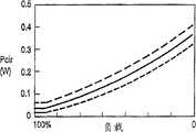
附图7表明了根据本发明描绘的负载与转换器的流通能量之间的关系的图表;Figure 7 shows a graph depicting the relationship between the load and the energy flowing through the converter according to the invention;
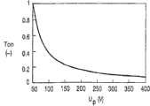
附图8表明了根据本发明描绘的初级电压与初级开关的接通时间之间的关系的图表;Figure 8 shows a graph depicting the relationship between the primary voltage and the turn-on time of the primary switch according to the present invention;
附图9表明了包括转换器的显示设备;Accompanying drawing 9 shows the display device that comprises converter;
在不同的附图中,同样的参考数字表示同样的元件或者具有同样功能的元件。In different drawings, the same reference numerals denote the same elements or elements with the same function.
具体实施方式Detailed ways
附图1是一个包括初级端口2以及次级端口4的降压转换器的一般的方框图。初级端口2的终端与一个电容6(可能是本征或者寄生电容,例如一个或者多个其它电路元件,诸如开关,的固有电容),一个二极管8以及一个初级开关构成的第一平行设备相耦合。初级开关的关闭和开启受初级开关控制电路12的控制,下文将进行详细的解释和讨论。次级端口4的终端与一个感应器14相耦合。由电容16(可能是本征或者寄生的),二极管18以及第二开关20构成的第二平行设备与第一平行设备以及感应器14相耦合。次级开关20的关闭和开启受次级开关控制电路22的控制,下文将进行详细的解释和讨论。而且,第二平行设备与初级端口2以及次级端口4的公共终端相耦合。FIG. 1 is a general block diagram of a buck converter including a primary port 2 and a secondary port 4 . The terminal of the primary port 2 is coupled to a capacitor 6 (which may be intrinsic or parasitic, such as the intrinsic capacitance of one or more other circuit elements, such as switches), a diode 8 and a first parallel device consisting of a primary switch . Turning off and on of the primary switch is controlled by the primary switch control circuit 12, which will be explained and discussed in detail below. The terminal of the secondary port 4 is coupled to an inductor 14 . A second parallel device consisting of a capacitor 16 (which may be intrinsic or parasitic), a diode 18 and a second switch 20 is coupled to the first parallel device and the inductor 14 . The closing and opening of the secondary switch 20 is controlled by the secondary switch control circuit 22, which will be explained and discussed in detail below. Furthermore, a second parallel device is coupled to a common terminal of the primary port 2 and the secondary port 4 .
附图2是一个包括初级端口32以及次级端口34的升压转换器的一般的方框图。初级端口32的终端与感应器36相耦合。感应器36背离初级端口32的一例与由电容38(可能是本征或者寄生的),二极管40以及初级开关42构成的第一平行设备相耦合。初级开关42的关闭和开启受初级开关控制电路44的控制,下文将进行详细的解释和讨论。由电容46(可能是本征或者寄生的),二极管48以及次级开关50构成的第二平行设备与第一平行设备,感应器36以及次级端口34的终端相耦合。次级开关50的关闭和开启受次级开关控制电路52的控制,下文将进行详细的解释和讨论。而且,第一平行设备与初级端口32以及次级端口34的公共终端相耦合。FIG. 2 is a generalized block diagram of a boost converter including a
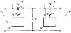
附图3是一个包括初级端口62以及次级端口64的双向回扫转换器的一般的方框图。初级端口62的终端与由一个电容66(可能是本征或者寄生电容),一个二极管68以及一个初级开关70构成的第一平行设备相耦合。初级开关70的关闭和开启受初级开关控制电路72的控制,下文将进行详细的解释和讨论。次级端口64的终端与一个由电容76(可能是本征或者寄生的),二极管78以及次级开关80构成的第二平行设备相耦合。次级开关80的关闭和开启受次级开关控制电路82的控制,下文将进行详细的解释和讨论。第一平行设备与第二平行设备与感应器84相耦合,其相对的一侧与初级端口62以及次级端口64的公共终端相耦合。FIG. 3 is a generalized block diagram of a bidirectional flyback converter including a
附图4是一个包括初级端口90以及次级端口92的双向回扫转换器的一般的方框图。初级端口的终端与变压器96的初级线圈94相耦合。初级线圈94串连连接到由二极管196和初级开关98构成的第一平行设备上。初级开关98的关闭和开启受初级开关控制电路100的控制,下文将进行详细的解释和讨论。次级端口的终端与变压器96的次级线圈102相耦合。次级线圈102串联连接到由二极管104和次级开关106构成的平行设备上。次级开关106的关闭和开启受次级开关控制电路108的控制,下文将进行详细的描述和解释。在一个实际的实施例中,开关98和106每一个都可以使用MOSFET,其中二极管196和104分别可以是固有的。MOSFET也可以具有一个本征电容。FIG. 4 is a generalized block diagram of a bidirectional flyback converter including a primary port 90 and a
在图1到图4所示的转换器中,输入到初级端口2,32,62以及90的初级电压Up被分别用作初级开关控制电路12,44,72以及100的输入控制变量,而输入到次级端口4,34,63以及92的次级电压Us和次级电流Is被分别用作第二开关控制电路22,52,82以及108的输入控制变量。正如在图5中将详细描述的,初级电压将与一个相应的参考电压相比较。产生的误差信号被用于控制控制初级电压的初级开关的接通时间。In the converters shown in Figures 1 to 4, the primary voltages Up input to the
次级电压Us和次级电流Is将与相应的参考值进行比较。产生的误差信号被用于控制次级开关的接通时间从而设定用于负载调整的次级能量的数量。次级能量的数量可以通过控制负的峰值电流或者有源开关的前向导通时间来确定。控制值与误差的偏移可以通过传统的技术实现,例如通过具有PI特性的误差放大方式。The secondary voltage Us and the secondary current Is are compared with corresponding reference values. The resulting error signal is used to control the on-time of the secondary switch to set the amount of secondary energy used for load regulation. The amount of secondary energy can be determined by controlling the negative peak current or the forward conduction time of the active switch. The offset of the control value and the error can be realized by conventional techniques, for example, by error amplification with PI characteristics.
一个表明与开关相联的二极管正在导通的附加信号允许有源开关在零电压的条件下被打开。附加信号可以是跨在有源开关以及与其相连的二极管的平行组合上的电压,或者是通过该组合的电流。附加信号可以通过传统的方法获得。An additional signal indicating that the diode associated with the switch is conducting allows the active switch to be turned on at zero voltage. The additional signal can be a voltage across the parallel combination of the active switch and the diode connected to it, or a current through the combination. Additional signals can be obtained by conventional methods.
在图4中,用于两个开关以及变压器电流的正确方向的控制信号之间的截止时间的使用导致了零电压转换。与转换相联系的损耗几乎被完全的消除。In Figure 4, the use of an off-time between the control signals for both switches and the correct direction of the transformer current results in a zero voltage transition. Losses associated with switching are almost completely eliminated.
附图5示出了双线回扫转化器的一部分,包括具有初级线圈94的变压器96。在图5中忽略了与变压器96的次级线圈102相耦合的电路。在图5中,以长划线表示的初级开关控制电路100被详细的示出。具体表示为MOSFET(包括一个本征反平行二极管)的初级开关设备110与变压器96的初级线圈94串连连结。转换控制输入或者MOSFET110的门与驱动器112的输出相耦合用于控制MOSFET的通断。驱动器112,本质上都为人们所熟知,因此这里将不再更为详细的示出,它具有一个输入,耦合到触发设备114的输出O。触发器设备114的复位输入端R耦合到比较器116的输出端,比较器116被提供给一个参考电压Uref。在比较器116中电压Uref与从电阻118和电容120的串连连接获得的跨接在转换器的初级端口122的输入的电压Uc相比较。一个旁路开关124与电容120并行连接,并由来自于触发设备114的反向输出信号Oinv控制其通断。元件112到120,124形成了初级开关设备110的初级开关控制电路100。FIG. 5 shows a portion of a two-wire flyback converter including a
初级开关控制电路100是如下的进行工作的。一个开始初级时钟被提供给触发设备114的设定输入端S。这样,触发设备即被设定,并且初级开关设备110通过驱动器112被打开。同时,旁路开关124被打开。结果是,通过电容120的电压上升到参考电压Uref。比较器116然后通过其输入端R重置触发设备114,并且结果是打开了初级开关设备110(初级时钟的末端),关闭旁路开关124,并且保持旁路开关的关闭状态使电容120放电,直至下一个初级时钟到来。初级开关设备的接通时间Ton根据下面的等式进行计算:The primary
Ton=R.C.Uref/UpTon=R.C.Uref/Up
其中:R=单位为Ω[欧姆]的电阻值Among them: R = resistance value in Ω [ohm]
C=单位为F[法]的电容值C = Capacitance value in F [method]
控制电路112到120,124可以是分离元件也可以被集成。The
附图6以粗体线示出了在0-100%的不同的负载条件下对于一个特定的转换器的正的峰值电流Ipeak,并且以普通的线示出了其负的峰值电流Ipeak,这里虚线表示在最小初级电压Up下的值,实线表示在额定初级电压Up下的值,并且粗线表示在最大初级电压Up下的值。Figure 6 shows the positive peak current Ipeak for a particular converter under different load conditions from 0-100% in bold lines, and its negative peak current Ipeak in normal lines, where The dashed line represents the value at the minimum primary voltage Up, the solid line represents the value at the rated primary voltage Up, and the thick line represents the value at the maximum primary voltage Up.
附图7示出了在0-100%的不同的负载条件下对于一个特定的转换器的流通能量Peir,其中虚线表示在最小初级电压Up下的值,实线表示在额定初级电压Up下的值,并且粗线表示在最大初级电压Up下的值。Figure 7 shows the flow-through energy Peir for a specific converter under different load conditions from 0-100%, where the dotted line represents the value at the minimum primary voltage Up, and the solid line represents the value at the rated primary voltage Up value, and the thick line represents the value at the maximum primary voltage Up.
附图6和7清楚的示出了使用本发明的控制方法的优点。对于所有的初级电压,在最大负载的情况下,负的峰值电流能够被调整到同样的值。因此,峰值电流以及流通能量都被最小化,这带来了比现有技术更为有效并且更加节省成本的转换器。Figures 6 and 7 clearly illustrate the advantages of using the control method of the present invention. For all primary voltages, the negative peak current can be adjusted to the same value at maximum load. Consequently, peak currents as well as passing energy are minimized, resulting in a more efficient and cost-effective converter than the prior art.
附图8示出了在理想的情况下(双曲形的)对于一个给定的设备在不同的初级电压Up的条件下的标准接通时间Ton。但是,描绘的曲线与垂直线交叉于标准的Ton的值1处的任何延时函数都是对于现有技术的一个进步。FIG. 8 shows the ideal (hyperbolic) standard turn-on time Ton for a given device at different primary voltages Up. However, any delay function where the plotted curve intersects the vertical line at the standard Ton value of 1 is an advance over the prior art.
根据本发明获得控制方法可以有不同的可能。取代在图5中解释的模拟解决方法,在一个数字设备中,初级电压Up能够被转换成数字值,其与表示在图8中示出的曲线的查找表相比较。这样,相应的Ton就能够被选择,并且计数器可以在由消磁信号获得的门打开信号下开始计数。在计数器达到零以后,开关设备被关闭并且计数器被一个新的更新值重装。There are different possibilities for obtaining a control method according to the invention. Instead of the analog solution explained in FIG. 5 , in a digital device the primary voltage Up can be converted into a digital value which is compared with a look-up table representing the curve shown in FIG. 8 . In this way, the corresponding Ton can be selected, and the counter can start counting under the gate open signal obtained from the degaussing signal. After the counter reaches zero, the switching device is closed and the counter is reloaded with a new updated value.
这样,根据本发明,转换器是这样受控的:转换器的初级侧的开关设备的接通时间依赖于施加在转换器的初级端口的电压而受控,通常在增加初级电压的时候接通时间会减少。以这种方法,可以得到转换器的较好的局部负载效率,同时在有限的开关频率内无负载浪费也较小。转换器的进一步的小型化也是可能的。Thus, according to the invention, the converter is controlled in such a way that the on-time of the switching device on the primary side of the converter is controlled in dependence on the voltage applied to the primary port of the converter, usually at the time of increasing the primary voltage Time will decrease. In this way, better partial load efficiency of the converter can be obtained with less no-load waste within the limited switching frequency. Further miniaturization of the converter is also possible.
附图9示出了具有转换器200,处理平台203以及显示设备205的显示设备。FIG. 9 shows a display device with a
转换器具有一个初级端口用于接收初级电压(例如,整流电源电压)以及一个次级端口用于提供次级电压。The converter has a primary port for receiving a primary voltage (eg, a rectified mains voltage) and a secondary port for providing a secondary voltage.
处理平台203接收视频输入信号206(例如,RGB+同步信号,或者复合视频信号),以及次级电压,其为一个能量提供电压,为显示设备提供驱动信号204。The processing platform 203 receives a video input signal 206 (eg, RGB+sync signal, or a composite video signal), and a secondary voltage, which is an energy supply voltage that provides a drive signal 204 for the display device.
显示设备205(例如一个阴极射线管,或者诸如液晶显示的显示阵列设备)显示与视频输入信号206相应的图像。A display device 205 (eg, a cathode ray tube, or a display array device such as a liquid crystal display) displays images corresponding to the video input signal 206 .
Claims (21)
Applications Claiming Priority (3)
| Application Number | Priority Date | Filing Date | Title |
|---|---|---|---|
| EP00203795 | 2000-10-27 | ||
| EP00203795.0 | 2000-10-27 | ||
| PCT/EP2001/011970WO2002035692A1 (en) | 2000-10-27 | 2001-10-16 | Converter control |
Publications (2)
| Publication Number | Publication Date |
|---|---|
| CN1394382A CN1394382A (en) | 2003-01-29 |
| CN1394382Btrue CN1394382B (en) | 2010-06-16 |
Family
ID=8172204
Family Applications (1)
| Application Number | Title | Priority Date | Filing Date |
|---|---|---|---|
| CN018033202AExpired - Fee RelatedCN1394382B (en) | 2000-10-27 | 2001-10-16 | Converter and control method thereof |
Country Status (6)
| Country | Link |
|---|---|
| US (1) | US6717388B2 (en) |
| EP (1) | EP1329016A1 (en) |
| JP (1) | JP2004512798A (en) |
| KR (1) | KR20020074177A (en) |
| CN (1) | CN1394382B (en) |
| WO (1) | WO2002035692A1 (en) |
Families Citing this family (38)
| Publication number | Priority date | Publication date | Assignee | Title |
|---|---|---|---|---|
| US20030155894A1 (en)* | 2002-02-07 | 2003-08-21 | International Rectifier Corporation | DC to DC converter with tapped inductor |
| CA2486179A1 (en)* | 2002-05-16 | 2003-11-27 | Ballard Power Systems Inc. | Electric power plant with adjustable array of fuel cell systems |
| US6788555B2 (en)* | 2002-09-26 | 2004-09-07 | Koninklijke Philips Electronics N.V. | Regulation of bi-directional flyback converter |
| CN1332587C (en) | 2003-02-07 | 2007-08-15 | 西班牙电子医药质量公司 | X-ray apparatus |
| US7632583B2 (en)* | 2003-05-06 | 2009-12-15 | Ballard Power Systems Inc. | Apparatus for improving the performance of a fuel cell electric power system |
| US7419734B2 (en)* | 2003-05-16 | 2008-09-02 | Ballard Power Systems, Inc. | Method and apparatus for fuel cell systems |
| US7102251B2 (en)* | 2003-08-22 | 2006-09-05 | Distributed Power, Inc. | Bi-directional multi-port inverter with high frequency link transformer |
| US7521138B2 (en)* | 2004-05-07 | 2009-04-21 | Ballard Power Systems Inc. | Apparatus and method for hybrid power module systems |
| US20050249989A1 (en)* | 2004-05-07 | 2005-11-10 | Pearson Martin T | Apparatus and method for hybrid power module systems |
| US7615981B2 (en)* | 2004-06-09 | 2009-11-10 | O2Micro International Limited | Boost converter with enhanced control capabilities of emulating an inductor current |
| US7280376B2 (en)* | 2004-10-15 | 2007-10-09 | Dell Products L.P. | Primary side voltage sense for AC/DC power supplies capable of compensation for a voltage drop in the secondary |
| KR101152118B1 (en) | 2005-02-16 | 2012-06-15 | 삼성전자주식회사 | Driving apparatus of display device and dc-dc converter |
| KR100722964B1 (en)* | 2005-04-21 | 2007-05-30 | 소시에다드 에스파뇰라 데 일렉트로메디시나 와이 칼리다드 에스.에이. | X-ray equipment |
| US7646616B2 (en)* | 2005-05-09 | 2010-01-12 | Allegro Microsystems, Inc. | Capacitor charging methods and apparatus |
| US7787262B2 (en)* | 2005-05-09 | 2010-08-31 | Allegro Microsystems, Inc. | Capacitor charging methods and apparatus |
| EP1804368A1 (en)* | 2005-12-29 | 2007-07-04 | Austriamicrosystems AG | Method for DC/DC conversion and DC/DC converter arrangement |
| US7382113B2 (en)* | 2006-03-17 | 2008-06-03 | Yuan Ze University | High-efficiency high-voltage difference ratio bi-directional converter |
| DE602006018874D1 (en)* | 2006-05-15 | 2011-01-27 | Austriamicrosystems Ag | Voltage generator arrangement and method for voltage conversion |
| CA2567562C (en)* | 2006-11-10 | 2010-01-12 | Psion Teklogix Inc. | Supercapacitor backup power supply with bi-directional power flow |
| US7915866B2 (en)* | 2006-11-13 | 2011-03-29 | Psion Teklogix Inc. | Supercapacitor backup power supply with bi-directional power flow |
| EP2009776A1 (en)* | 2007-06-26 | 2008-12-31 | Austriamicrosystems AG | Buck-boost switching regulator and method thereof |
| US8222874B2 (en) | 2007-06-26 | 2012-07-17 | Vishay-Siliconix | Current mode boost converter using slope compensation |
| EP2028752B1 (en)* | 2007-08-20 | 2011-03-09 | austriamicrosystems AG | DC/DC converter arrangement and method for DC/DC conversion |
| DE102007058314B4 (en)* | 2007-12-04 | 2018-11-15 | Diehl Aerospace Gmbh | Device for measuring a load current |
| US8570769B2 (en)* | 2009-12-21 | 2013-10-29 | Intersil Americas LLC | Bidirectional signal conversion |
| US8971073B2 (en) | 2010-03-23 | 2015-03-03 | Northrop Grumman Systems Corporation | System and method for providing a high efficiency bypass circuit for multi-stage DC-DC converters used in battery powered systems |
| CN101860200A (en)* | 2010-04-27 | 2010-10-13 | 华为技术有限公司 | Power-fail holding circuit, method and power supply system |
| US8498172B1 (en) | 2010-08-31 | 2013-07-30 | Western Digital Technologies, Inc. | Data storage device evaluating frequency range of supply voltage to detect power failure |
| US8754616B2 (en)* | 2011-02-11 | 2014-06-17 | Fairchild Semiconductor Corporation | Boost converter with multi-mode synchronous rectifier |
| US8941264B2 (en)* | 2011-06-20 | 2015-01-27 | Bae Systems Information And Electronic Systems Integration Inc. | Apparatus for bi-directional power switching in low voltage vehicle power distribution systems |
| FR2977119B1 (en)* | 2011-06-24 | 2017-06-16 | Valeo Japan Co Ltd | PRINTED CIRCUIT BOARD FOR COMPRESSOR HOUSING |
| US9618004B2 (en)* | 2012-01-25 | 2017-04-11 | Lg Electronics Inc. | Apparatus and method for using a microcomputer and switches to control the flow path for the power of a compressor based upon the compressor's load state |
| EP2944018B1 (en)* | 2013-01-14 | 2018-10-31 | Cognipower, LLC | Flyback amplifier with direct feedback |
| JP6020931B2 (en) | 2013-11-11 | 2016-11-02 | 株式会社デンソー | Power converter |
| JP6361479B2 (en)* | 2014-02-07 | 2018-07-25 | 株式会社デンソー | Power converter |
| KR101665937B1 (en)* | 2015-02-26 | 2016-10-13 | 유니온라이트 주식회사 | High-voltage series connected bi-directional converter |
| DE102016226001A1 (en)* | 2016-12-22 | 2018-06-28 | Osram Gmbh | CONTROL UNIT WITH A TWIN POINT REGULATOR FOR REGULATING A CONTACTED TRANSDUCER |
| US11070131B2 (en)* | 2018-01-24 | 2021-07-20 | Texas Instruments Incorporated | Methods, apparatus and circuits to control timing for hysteretic current-mode boost converters |
Citations (6)
| Publication number | Priority date | Publication date | Assignee | Title |
|---|---|---|---|---|
| US3986097A (en)* | 1975-06-30 | 1976-10-12 | Bell Telephone Laboratories, Incorporated | Bilateral direct current converters |
| US5220492A (en)* | 1989-12-26 | 1993-06-15 | Systel Development And Industries Ltd. | Inverter and power supply systems including same |
| AT399432B (en)* | 1991-09-05 | 1995-05-26 | Siemens Ag Oesterreich | Flyback converter |
| US5745351A (en)* | 1995-01-13 | 1998-04-28 | Sextant Avionique | DC-to-DC bidirectional voltage converters and current sensor |
| US5764495A (en)* | 1996-05-01 | 1998-06-09 | Compaq Computer Corporation | Variable-frequency variable-input-voltage converter with minimum frequency limit |
| US6084784A (en)* | 1998-06-24 | 2000-07-04 | U.S. Philips Corporation | Switched mode power supply with reduced reflected power |
Family Cites Families (30)
| Publication number | Priority date | Publication date | Assignee | Title |
|---|---|---|---|---|
| US4168477A (en)* | 1978-02-21 | 1979-09-18 | Gould Advance Limited | Electric regulators |
| EP0013332A1 (en)* | 1979-01-16 | 1980-07-23 | Siemens-Albis Aktiengesellschaft | Chopper circuit |
| US4347474A (en)* | 1980-09-18 | 1982-08-31 | The United States Of America As Represented By The Secretary Of The Navy | Solid state regulated power transformer with waveform conditioning capability |
| JPS5765266A (en)* | 1980-10-07 | 1982-04-20 | Fuji Electric Co Ltd | Switching regulator |
| JPS57156668A (en)* | 1981-03-20 | 1982-09-28 | Sanken Electric Co Ltd | Conversion of dc |
| US4672303A (en)* | 1986-08-28 | 1987-06-09 | International Business Machines Corporation | Inductor current control circuit |
| US4801859A (en)* | 1986-12-23 | 1989-01-31 | Sundstrand Corporation | Boost/buck DC/DC converter |
| US4736151A (en)* | 1986-12-23 | 1988-04-05 | Sundstrand Corporation | Bi-directional buck/boost DC/DC converter |
| JPS63174560A (en)* | 1987-01-13 | 1988-07-19 | Fujitsu Ltd | DC/DC converter |
| DE3713540A1 (en)* | 1987-04-22 | 1988-11-10 | Siemens Ag | COMBINED SECONDARY SWITCH |
| JP2773195B2 (en)* | 1988-04-05 | 1998-07-09 | 松下電器産業株式会社 | Switching power supply |
| IT1225633B (en)* | 1988-11-30 | 1990-11-22 | Sgs Thomson Microelectronics | PROTECTION FROM NETWORK TRANSITORS. |
| US4931716A (en)* | 1989-05-05 | 1990-06-05 | Milan Jovanovic | Constant frequency zero-voltage-switching multi-resonant converter |
| US5066900A (en)* | 1989-11-14 | 1991-11-19 | Computer Products, Inc. | Dc/dc converter switching at zero voltage |
| DE4105464A1 (en)* | 1990-04-26 | 1991-10-31 | Siemens Ag | CLOCKED INVERTER WITH CONTROL OF FOLLOW-UP FREQUENCY AND DURATION |
| US5208740A (en)* | 1991-05-30 | 1993-05-04 | The Texas A & M University System | Inverse dual converter for high-power applications |
| JP3294343B2 (en)* | 1992-11-13 | 2002-06-24 | 松下電工株式会社 | Power supply |
| US5479089A (en)* | 1994-12-21 | 1995-12-26 | Hughes Aircraft Company | Power converter apparatus having instantaneous commutation switching system |
| JPH0973990A (en)* | 1995-09-04 | 1997-03-18 | Minebea Co Ltd | Cold cathode tube lighting device using piezo-electric transformer |
| US5844399A (en)* | 1996-07-26 | 1998-12-01 | The University Of Toledo | Battery charger control system |
| GB2335317A (en)* | 1998-03-11 | 1999-09-15 | Simon Richard Greenwood | Bi-directional voltage converter |
| US6008630A (en)* | 1998-07-02 | 1999-12-28 | Compact Computer Corporation | Soft-switched built-in active snubber circuit |
| US6069804A (en)* | 1998-07-28 | 2000-05-30 | Condor D.C. Power Supplies, Inc. | Bi-directional dc-to-dc power converter |
| US6058026A (en)* | 1999-07-26 | 2000-05-02 | Lucent Technologies, Inc. | Multiple output converter having a single transformer winding and independent output regulation |
| US6194880B1 (en)* | 1999-10-22 | 2001-02-27 | Lucent Technologies Inc. | Boost converter, method of converting power and power supply employing the same |
| US6232752B1 (en)* | 1999-11-10 | 2001-05-15 | Stephen R. Bissell | DC/DC converter with synchronous switching regulation |
| GB2357641B (en)* | 1999-12-20 | 2002-02-20 | Motorola Ltd | DC-DC Converter and energy management system |
| JP3626072B2 (en)* | 2000-05-31 | 2005-03-02 | 松下電器産業株式会社 | Switching power supply |
| JP4395881B2 (en)* | 2000-09-06 | 2010-01-13 | Tdkラムダ株式会社 | Synchronous rectifier circuit for switching power supply |
| US6366070B1 (en)* | 2001-07-12 | 2002-04-02 | Analog Devices, Inc. | Switching voltage regulator with dual modulation control scheme |
- 2001
- 2001-10-16CNCN018033202Apatent/CN1394382B/ennot_activeExpired - Fee Related
- 2001-10-16EPEP01988969Apatent/EP1329016A1/ennot_activeWithdrawn
- 2001-10-16WOPCT/EP2001/011970patent/WO2002035692A1/ennot_activeApplication Discontinuation
- 2001-10-16JPJP2002538557Apatent/JP2004512798A/ennot_activeCeased
- 2001-10-16KRKR1020027008207Apatent/KR20020074177A/ennot_activeCeased
- 2001-10-25USUS10/144,818patent/US6717388B2/ennot_activeExpired - Fee Related
Patent Citations (6)
| Publication number | Priority date | Publication date | Assignee | Title |
|---|---|---|---|---|
| US3986097A (en)* | 1975-06-30 | 1976-10-12 | Bell Telephone Laboratories, Incorporated | Bilateral direct current converters |
| US5220492A (en)* | 1989-12-26 | 1993-06-15 | Systel Development And Industries Ltd. | Inverter and power supply systems including same |
| AT399432B (en)* | 1991-09-05 | 1995-05-26 | Siemens Ag Oesterreich | Flyback converter |
| US5745351A (en)* | 1995-01-13 | 1998-04-28 | Sextant Avionique | DC-to-DC bidirectional voltage converters and current sensor |
| US5764495A (en)* | 1996-05-01 | 1998-06-09 | Compaq Computer Corporation | Variable-frequency variable-input-voltage converter with minimum frequency limit |
| US6084784A (en)* | 1998-06-24 | 2000-07-04 | U.S. Philips Corporation | Switched mode power supply with reduced reflected power |
Non-Patent Citations (1)
| Title |
|---|
| 同上. |
Also Published As
| Publication number | Publication date |
|---|---|
| US6717388B2 (en) | 2004-04-06 |
| US20020190698A1 (en) | 2002-12-19 |
| JP2004512798A (en) | 2004-04-22 |
| WO2002035692A1 (en) | 2002-05-02 |
| CN1394382A (en) | 2003-01-29 |
| KR20020074177A (en) | 2002-09-28 |
| EP1329016A1 (en) | 2003-07-23 |
Similar Documents
| Publication | Publication Date | Title |
|---|---|---|
| CN1394382B (en) | Converter and control method thereof | |
| US10218256B2 (en) | Primary side control of primary resonant flyback converters | |
| US7023186B2 (en) | Two stage boost converter topology | |
| US6344986B1 (en) | Topology and control method for power factor correction | |
| US7015561B2 (en) | Active rectifier | |
| US7915876B2 (en) | Power converter with snubber | |
| US4720668A (en) | Zero-voltage switching quasi-resonant converters | |
| US7965523B2 (en) | Switching power supply device | |
| US4652984A (en) | Self-oscillating power-supply circuit | |
| US6906930B2 (en) | Structure and method for an isolated boost converter | |
| GB2451088A (en) | Regulating the output of a forward power converter | |
| EP0518300A1 (en) | Power supply circuit | |
| US20090097291A1 (en) | Universal power supply for a laptop | |
| US20070297199A1 (en) | Multi-Resonance Converter | |
| WO2022031785A1 (en) | Soft-start for switching converter controller with hybrid hyseretic control (hhc) | |
| CN101156305A (en) | Method for operating switched-mode power supply components with primary-side leakage energy feedback | |
| US6282103B1 (en) | Switching power supply using an inductor device to prevent harmonic current generation | |
| JP2004531198A (en) | Bidirectional flyback switch mode power supply (SMPS) | |
| US6625042B2 (en) | Power supply arrangement comprising a DC/DC converter with primary-side control loop | |
| EP1001514A2 (en) | Switched power converter with hold-up time and harmonics reduction | |
| US7092260B2 (en) | Short-circuiting rectifier for a switched-mode power supply | |
| US12074528B2 (en) | Secondary side controlled QR flyback converter using a programmable valley algorithm | |
| KR100420964B1 (en) | Single-stage converter compensating power factor | |
| US11444531B2 (en) | Voltage converter | |
| US5703763A (en) | Power supply apparatus with improved efficiency |
Legal Events
| Date | Code | Title | Description |
|---|---|---|---|
| C06 | Publication | ||
| PB01 | Publication | ||
| C10 | Entry into substantive examination | ||
| SE01 | Entry into force of request for substantive examination | ||
| C14 | Grant of patent or utility model | ||
| GR01 | Patent grant | ||
| C17 | Cessation of patent right | ||
| CF01 | Termination of patent right due to non-payment of annual fee | Granted publication date:20100616 Termination date:20121016 |