CN1366308A - Semiconductor storage formed for optimizing testing technique and rebundance technique - Google Patents
Semiconductor storage formed for optimizing testing technique and rebundance techniqueDownload PDFInfo
- Publication number
- CN1366308A CN1366308ACN02101900ACN02101900ACN1366308ACN 1366308 ACN1366308 ACN 1366308ACN 02101900 ACN02101900 ACN 02101900ACN 02101900 ACN02101900 ACN 02101900ACN 1366308 ACN1366308 ACN 1366308A
- Authority
- CN
- China
- Prior art keywords
- enabled
- word line
- signal
- word lines
- memory device
- Prior art date
- Legal status (The legal status is an assumption and is not a legal conclusion. Google has not performed a legal analysis and makes no representation as to the accuracy of the status listed.)
- Granted
Links
Images


Classifications
- G—PHYSICS
- G11—INFORMATION STORAGE
- G11C—STATIC STORES
- G11C29/00—Checking stores for correct operation ; Subsequent repair; Testing stores during standby or offline operation
- G11C29/70—Masking faults in memories by using spares or by reconfiguring
- G11C29/78—Masking faults in memories by using spares or by reconfiguring using programmable devices
- G11C29/785—Masking faults in memories by using spares or by reconfiguring using programmable devices with redundancy programming schemes
- G—PHYSICS
- G11—INFORMATION STORAGE
- G11C—STATIC STORES
- G11C29/00—Checking stores for correct operation ; Subsequent repair; Testing stores during standby or offline operation
- G—PHYSICS
- G11—INFORMATION STORAGE
- G11C—STATIC STORES
- G11C29/00—Checking stores for correct operation ; Subsequent repair; Testing stores during standby or offline operation
- G11C29/04—Detection or location of defective memory elements, e.g. cell constructio details, timing of test signals
- G11C29/08—Functional testing, e.g. testing during refresh, power-on self testing [POST] or distributed testing
- G11C29/12—Built-in arrangements for testing, e.g. built-in self testing [BIST] or interconnection details
- G11C29/18—Address generation devices; Devices for accessing memories, e.g. details of addressing circuits
- G11C29/26—Accessing multiple arrays
- G—PHYSICS
- G11—INFORMATION STORAGE
- G11C—STATIC STORES
- G11C29/00—Checking stores for correct operation ; Subsequent repair; Testing stores during standby or offline operation
- G11C29/70—Masking faults in memories by using spares or by reconfiguring
- G11C29/78—Masking faults in memories by using spares or by reconfiguring using programmable devices
- G11C29/785—Masking faults in memories by using spares or by reconfiguring using programmable devices with redundancy programming schemes
- G11C29/787—Masking faults in memories by using spares or by reconfiguring using programmable devices with redundancy programming schemes using a fuse hierarchy
- G—PHYSICS
- G11—INFORMATION STORAGE
- G11C—STATIC STORES
- G11C29/00—Checking stores for correct operation ; Subsequent repair; Testing stores during standby or offline operation
- G11C29/04—Detection or location of defective memory elements, e.g. cell constructio details, timing of test signals
- G11C29/08—Functional testing, e.g. testing during refresh, power-on self testing [POST] or distributed testing
- G11C29/12—Built-in arrangements for testing, e.g. built-in self testing [BIST] or interconnection details
- G11C29/18—Address generation devices; Devices for accessing memories, e.g. details of addressing circuits
- G11C29/26—Accessing multiple arrays
- G11C2029/2602—Concurrent test
Landscapes
- For Increasing The Reliability Of Semiconductor Memories (AREA)
- Dram (AREA)
- Techniques For Improving Reliability Of Storages (AREA)
Abstract
Translated fromChineseDescription
Translated fromChinese技术领域technical field
本发明涉及半导体存储器件,特别是涉及目的在于优化测试技术和冗余技术的半导体存储器件。The present invention relates to semiconductor memory devices, and more particularly to semiconductor memory devices aimed at optimizing testing techniques and redundancy techniques.
背景技术Background technique
近来,半导体存储器件的存储容量一直在增加,并且各种用来测试半导体存储器件是否正确操作的测试技术及用来修补(补偿)半导体存储器件的缺陷的冗余技术变得很重要。在大存储容量的半导体存储器件中,压缩进行各种功能测试的测试时间和提高修补半导体存储器件的缺陷的冗余技术的效率及降低其成本是很关键的。Recently, the storage capacity of semiconductor memory devices has been increasing, and various testing techniques for testing whether semiconductor memory devices operate correctly and redundancy techniques for repairing (compensating for) defects of semiconductor memory devices have become important. In semiconductor memory devices with large storage capacity, it is critical to compress the test time for performing various functional tests and to improve the efficiency and reduce the cost of redundancy techniques for repairing defects of semiconductor memory devices.
然而,优化测试技术和冗余技术是很困难的,并且如果试图测试一个经过利用冗余技术修补过的半导体存储器件,那么测试时间会变得更长,而且测试操作变得很困难,并且如果试图减少测试时间,则高效低成本的冗余技术无法实施。However, it is difficult to optimize the test technique and the redundancy technique, and if an attempt is made to test a semiconductor memory device that has been patched with the redundancy technique, the test time becomes longer and the test operation becomes difficult, and if Efficient and low-cost redundancy techniques cannot be implemented in an attempt to reduce test time.
发明内容Contents of the invention
据此,本发明的一个目的是提供一种测试技术和冗余技术可以得到优化的半导体存储器件。Accordingly, an object of the present invention is to provide a semiconductor memory device in which testing techniques and redundancy techniques can be optimized.
本发明的另一个目的是提供一种测试时间可以减少而功能测试可以简化的半导体存储器件。Another object of the present invention is to provide a semiconductor memory device in which test time can be reduced and functional testing can be simplified.
本发明的再一个目的是提供一种可以实施高效低成本冗余技术测试技术的半导体存储器件。Another object of the present invention is to provide a semiconductor memory device capable of implementing high-efficiency and low-cost redundancy technology testing techniques.
此外,本发明的另一个目的是提供一种即使是实施高效低成本冗余技术测试技术和冗余技术测试时间也可以减少而功能测试也可以简化的半导体存储器件。Furthermore, another object of the present invention is to provide a semiconductor memory device in which a redundant technology test time can be reduced and a functional test can be simplified even if a high-efficiency and low-cost redundant technology testing technology is implemented.
根据本发明的一个方面,所提供的半导体存储器件是其中只是缺陷元件由行冗余元件替换以补偿缺陷,条件是如果多个元件中至少有一个在单元阵列部件中的多个元件同时启用的场合是有缺陷的,其构成包括配置成为可通过根据一个确定行冗余替换是否执行的信号来防止字线状态信号被接收而中断缺陷元件的操作阵列控制电路,其中字线状态信号是经单信号线输入到单元阵列部件中的多个存储块中。According to an aspect of the present invention, there is provided a semiconductor memory device in which only a defective element is replaced by a row redundant element to compensate for the defect, provided that at least one of the plurality of elements is enabled simultaneously in the cell array unit The occasion is defective, comprising array control circuitry configured to interrupt the operation of a defective element by preventing the reception of a word line status signal based on a signal determining whether row redundancy replacement is performed, wherein the word line status signal is transmitted via a single Signal lines are input to a plurality of memory blocks in the cell array unit.
根据本发明的另一个方面,所提供的半导体存储器件是其中只是缺陷元件由行冗余元件替换以补偿缺陷,条件是如果多个元件中至少有一个在单元阵列部件中的多个(2n:n是自然数)元件同时启用的场合是有缺陷的,其构成包括n个传输代表同时启用的元件中的任何一个的数据信号的信号线,当发现其有缺陷并应该由行冗余元件替换,以及一个阵列控制电路,该阵列控制电路配置成为用来对经n个信号线传输的信号进行本地译码并把在多个元件中选择的一个元件设置为禁止态。According to another aspect of the present invention, there is provided a semiconductor memory device in which only defective elements are replaced by row redundant elements to compensate for defects, provided that if at least one of the plurality of elements is in a plurality (2n : n is a natural number) The occasions where the elements are enabled at the same time are defective, which constitutes n signal lines that transmit data signals representing any one of the elements that are simultaneously enabled, when found to be defective and should be replaced by row redundant elements , and an array control circuit configured to locally decode signals transmitted through the n signal lines and set a selected one of the plurality of elements to a disabled state.
根据本发明的再一个方面,所提供的半导体存储器件是其中只是缺陷元件由行冗余元件替换以补偿缺陷,条件是如果多个元件中至少有一个在单元阵列部件中的多个(2n:n是自然数)元件同时启用的场合是有缺陷的,其构成包括传输指示多个元件的启用和停用的字线状态信号的第一信号线,传输指示出现缺陷元件被行冗余元件替换的冗余替换现象的第二信号线,n个传输具有指示有待同时启用的多个元件中的哪一个在由行冗余元件替换缺陷元件时被替换的地址信息的信号的第三信号线,条件是多个元件中至少有一个是有缺陷的,以及一个阵列控制电路,该阵列控制电路配置成为用来对经n个第三信号线传输的信号为每个存储块进行译码,其中冗余元件设置为启用态,而缺陷元件设置为停用态并利用阵列控制电路由行冗余元件替换,条件是多个元件中至少有一个是有缺陷的。According to still another aspect of the present invention, there is provided a semiconductor memory device in which only defective elements are replaced by row redundant elements to compensate for defects, provided that if at least one of the plurality of elements is in a plurality (2n : n is a natural number) the occasion that the element is enabled at the same time is defective, and its composition includes the first signal line of the word line state signal that transmits the enabling and disabling of multiple elements, and the transmission indicates that the defective element is replaced by a row redundant element second signal lines of the redundant replacement phenomenon, n third signal lines transmitting signals having address information indicating which one of the plurality of elements to be simultaneously activated is replaced when a defective element is replaced by a row redundant element, The condition is that at least one of the plurality of elements is defective, and an array control circuit configured to decode signals transmitted through n third signal lines for each memory block, wherein the redundant The remaining elements are set to an enabled state, and defective elements are set to a disabled state and replaced by row redundant elements using the array control circuitry, provided that at least one of the plurality of elements is defective.
根据本发明的一个方面,所提供的半导体存储器件是其中只是缺陷元件由行冗余元件替换以补偿缺陷,条件是如果多个元件中至少有一个在单元阵列部件中的多个元件同时启用的场合是有缺陷的,其构成包括配置成为可在不同时间同时启用多个字线从而选择字线的操作模式下保持地址数据和冗余数据的锁存电路。According to an aspect of the present invention, there is provided a semiconductor memory device in which only a defective element is replaced by a row redundant element to compensate for the defect, provided that at least one of the plurality of elements is enabled simultaneously in the cell array unit Occasionally, it is defective that the composition includes a latch circuit configured to hold address data and redundant data in an operation mode in which a plurality of word lines are simultaneously enabled at different times to select a word line.
根据本发明的一个方面,所提供的半导体存储器件是其中只是缺陷元件由行冗余元件替换以补偿缺陷,条件是如果多个元件中至少有一个在单元阵列部件中的多个元件同时启用的场合是有缺陷的,其构成包括一个阵列控制电路,该阵列控制电路配置成为可设置行冗余元件为启用态,设置缺陷元件为停用态并由冗余元件替换该缺陷元件,条件是多个元件中至少有一个是有缺陷的,该阵列控制电路的构成包括第一锁存电路,该第一锁存电路配置成为可保持现在状态一直到接收到预充电命令,条件是在不同时间同时启用多个字线从而启用字线的操作模式下接收到阵列控制电路状态信号,包括配置成为可保持读出放大器(读放大器)的启用/停用态的第二锁存电路,包括第三锁存电路,该第三锁存电路配置成为可在不同时间同时启用多个字线从而启用字线的操作模式下保持字线启用信号,以及包括配置成为可保持用来控制行译码器的状态的信号的第四锁存电路。According to an aspect of the present invention, there is provided a semiconductor memory device in which only a defective element is replaced by a row redundant element to compensate for the defect, provided that at least one of the plurality of elements is enabled simultaneously in the cell array unit The occasion is defective, consisting of an array control circuit configured to set a row redundant element to an enabled state, to set a defective element to an inactive state and to replace the defective element with a redundant element, provided that more At least one of the elements is defective, and the array control circuit is composed of a first latch circuit configured to maintain the present state until a precharge command is received, provided that at different times simultaneously A plurality of word lines are enabled so that an array control circuit status signal is received in the word line enabled mode of operation, including a second latch circuit configured to maintain an enabled/disabled state of a sense amplifier (sense amplifier), including a third latch circuit A storage circuit, the third latch circuit is configured to simultaneously enable a plurality of word lines at different times so as to maintain the word line enable signal in the operation mode of enabling the word line, and includes a state configured to maintain the state used to control the row decoder signal to the fourth latch circuit.
根据本发明的一个方面,所提供的半导体存储器件是其中只是缺陷元件由行冗余元件替换以补偿缺陷,条件是如果多个元件中至少有一个在单元阵列部件中的多个元件同时启用的场合是有缺陷的,其构成包括一个阵列控制电路,该阵列控制电路配置成为可设置行冗余元件为启用态,设置缺陷元件为停用态并由冗余元件替换该缺陷元件,条件是多个元件中至少有一个是有缺陷的,该阵列控制电路的构成包括第一锁存电路,该第一锁存电路配置成为可保持现在状态一直到接收到预充电命令,条件是在不同时间同时启用多个字线从而启用字线的操作模式下接收到阵列控制电路状态信号,包括配置成为可保持读出放大器(读放大器)的启用/停用态的第二锁存电路,包括第三锁存电路,该第三锁存电路配置成为可在不同时间同时启用多个字线从而在启用字线的操作模式下保持字线启用信号,以及包括配置成为控制行译码器的状态的控制电路。According to an aspect of the present invention, there is provided a semiconductor memory device in which only a defective element is replaced by a row redundant element to compensate for the defect, provided that at least one of the plurality of elements is enabled simultaneously in the cell array unit The occasion is defective, consisting of an array control circuit configured to set a row redundant element to an enabled state, to set a defective element to an inactive state and to replace the defective element with a redundant element, provided that more At least one of the elements is defective, and the array control circuit is composed of a first latch circuit configured to maintain the present state until a precharge command is received, provided that at different times simultaneously A plurality of word lines are enabled so that an array control circuit status signal is received in the word line enabled mode of operation, including a second latch circuit configured to maintain an enabled/disabled state of a sense amplifier (sense amplifier), including a third latch circuit a storage circuit, the third latch circuit is configured to simultaneously enable a plurality of word lines at different times so as to maintain the word line enable signal in the word line enabled operation mode, and includes a control circuit configured to control the state of the row decoder .
根据本发明的一个方面,所提供的半导体存储器件是其中多个字线通过使一旦启用的每个字线在多个连续的字线选择循环中保持启用态而一起启用,其构成包括一个锁存电路,该锁存电路配置成为提取地址信息以指定待选的字线并提取冗余信息用来指示在每个字线选择循环中地址信息指定的地址是否与预编程地址符合并在冗余不符合时启用和保持用来在指定的循环中选择由地址信息指定的字线启用信号。According to one aspect of the present invention, there is provided a semiconductor memory device in which a plurality of word lines are enabled together by keeping each word line once enabled in an enabled state for a plurality of consecutive word line selection cycles, the configuration comprising a lock A storage circuit configured to extract address information to specify a word line to be selected and to extract redundant information to indicate whether the address specified by the address information in each word line selection cycle is consistent with a pre-programmed address and in redundant Enable and Hold are used to select the word line enable signal specified by the address information in a specified cycle.
根据本发明的一个方面,所提供的半导体存储器件是其中多个字线通过使一旦启用的每个字线在多个连续的字线选择循环中保持启用态而一起启用,其构成包括一个功能电路,该功能电路配置成为可在一个周期中连续保持冗余命中信息,在该周期中在一旦访问的字线是缺陷字线的场合选择字线并设置缺陷字线为非选态。According to an aspect of the present invention, there is provided a semiconductor memory device in which a plurality of word lines are enabled together by keeping each word line once enabled in an enabled state for a plurality of consecutive word line selection cycles, the constitution of which includes a function The circuit, the functional circuit is configured to continuously maintain redundant hit information in a cycle, in which the word line is selected and the defective word line is set to a non-selected state if the once accessed word line is a defective word line.
根据本发明的一个方面,所提供的半导体存储器件是其中多个字线通过使一旦启用的每个字线在多个连续的字线选择循环中保持启用态而一起启用,其构成包括一个锁存电路,该锁存电路配置成为可在存储块被访问和冗余首先失败时导出启用信号的逻辑AND并导出在每个循环中产生的用来确定在每个循环中启用读出放大器的定时的信号,生成读出放大器启用信号并保持该信息。According to one aspect of the present invention, there is provided a semiconductor memory device in which a plurality of word lines are enabled together by keeping each word line once enabled in an enabled state for a plurality of consecutive word line selection cycles, the configuration comprising a lock A latch circuit configured to derive a logical AND of the enable signal when the memory block is accessed and redundancy first fails and to derive the timing generated in each cycle to determine the timing of enabling the sense amplifier in each cycle , generate a sense amplifier enable signal and hold this information.
根据本发明的一个方面,所提供的半导体存储器件具有一起启用通过单元晶体管连接到同一位线的多个字线的功能,其构成包括一个列冗余系统,该列冗余系统根据行地址设置列冗余的修补区,其中修补区的设置是为了在修补区设置用来分割位线时允许一起启用的字线属于同一修补区。According to one aspect of the present invention, there is provided a semiconductor memory device having a function of collectively enabling a plurality of word lines connected to the same bit line through cell transistors, and its constitution includes a column redundancy system set according to a row address A column redundant repair area, wherein the repair area is set to allow word lines enabled together to belong to the same repair area when the repair area is set to divide bit lines.
根据本发明的一个方面,所提供的半导体存储器件的构成包括一个列冗余系统,该列冗余系统根据行地址设置列冗余的修补区,其中修补区的设置是为了使在一个操作模式下在一个修补区内可一起启用的字线数最大,该操作模式可在存储器单元阵列中的列修补区的大小固定和为了配置列修补区中的一个修补区而链接的每个分修补区的大小固定或小于字线数的条件下在多个连续的字线选择循环中保持一旦启用的字线为启用态。According to one aspect of the present invention, the composition of the provided semiconductor memory device includes a column redundancy system, and the column redundancy system sets the column redundant repair area according to the row address, wherein the repair area is set so that in an operation mode The number of word lines that can be enabled together in one repair area is the largest, and this operation mode can be fixed in the size of the column repair area in the memory cell array and each sub-repair area linked to configure a repair area in the column repair area The word line once enabled is kept in the enabled state for a plurality of consecutive word line selection cycles under the condition that the size of is fixed or less than the number of word lines.
根据本发明的一个方面,所提供的半导体存储器件的构成包括一个列冗余系统,该列冗余系统根据行地址设置列冗余的修补区,其中修补区的设置是为了使在一个操作模式下在一个修补区内可一起启用的字线数最大,该操作模式可在当修补区设置为分割位线时在列修补区的大小固定和分割一个位线的修补区数固定或小于列修补区大小的条件下在多个连续的字线选择循环中保持一旦启用的字线为启用态。According to one aspect of the present invention, the composition of the provided semiconductor memory device includes a column redundancy system, and the column redundancy system sets the column redundant repair area according to the row address, wherein the repair area is set so that in an operation mode The number of word lines that can be enabled together in a repair area is the largest. This operation mode can fix the size of the column repair area and the number of repair areas that divide a bit line when the repair area is set to split bit lines. A once enabled word line is kept enabled for multiple consecutive word line select cycles subject to the block size.
根据本发明的一个方面,所提供的半导体存储器件的构成包括一个列冗余系统,该列冗余系统根据行地址设置列冗余的修补区,其中修补区的设置是为了使在一个操作模式下在一个修补区内可一起启用的字线数最大,该操作模式可在列修补区的大小固定和为了配置列修补区中的一个修补区而链接的每个分修补区的大小固定或大于固定的大小和分割一个位线的修补区数固定或小于字线数的条件下在多个连续的字线选择循环中保持一旦启用的字线为启用态。According to one aspect of the present invention, the composition of the provided semiconductor memory device includes a column redundancy system, and the column redundancy system sets the column redundant repair area according to the row address, wherein the repair area is set so that in an operation mode The number of word lines that can be enabled together in one repair area is the largest, and this operation mode can be fixed in the size of the column repair area and the size of each sub-repair area linked to configure a repair area in the column repair area is fixed or greater than Once enabled word lines are kept enabled in a plurality of consecutive word line selection cycles under the condition that the size is fixed and the number of patching areas for dividing a bit line is fixed or less than the number of word lines.
根据本发明的一个方面,所提供的半导体存储器件的构成包括一个列冗余系统,该列冗余系统根据行地址设置列冗余的修补区,其中修补区的设置是为了使所有可以在下述操作模式中一起启用的字线属于同一修补区,该操作模式可在多个连续的字线选择循环中保持一旦启用的字线为启用态。According to one aspect of the present invention, the composition of the provided semiconductor memory device includes a column redundancy system, and the column redundancy system sets the repair area of column redundancy according to the row address, wherein the setting of the repair area is to make all the following The word lines enabled together in the operation mode belong to the same repair area, and the operation mode can keep the word lines enabled once enabled in a plurality of consecutive word line selection cycles.
根据本发明的一个方面,所提供的半导体存储器件的构成包括一个列冗余系统,该列冗余系统根据行地址设置列冗余的修补区,其中列冗余系统的功能包括在多个连续的字线选择循环中保持一旦启用的字线为启用态的操作模式中一起启用的多个字线有缺陷的场合只设置缺陷字线为停用态的功能,选择多个备用字线替换缺陷字线的功能,允许多个替换备用字线经单元晶体管连接到同一位线和只将备用字线设置为停用态的功能。According to one aspect of the present invention, the composition of the provided semiconductor memory device includes a column redundancy system, and the column redundancy system sets the column redundancy repair area according to the row address, wherein the function of the column redundancy system includes In the word line selection cycle, keep the enabled word line in the enabled state. In the operation mode, when multiple word lines enabled together are defective, only set the defective word line to the disabled state, and select multiple spare word lines to replace the defect. The function of the word line, the function of allowing multiple replacement spare word lines to be connected to the same bit line via the cell transistors and setting only the spare word line to the inactive state.
根据本发明的一个方面,所提供的列冗余系统是根据行地址设置列冗余的修补区,该列冗余系统的构成包括一个电路,该电路配置成为可在多个连续的字线选择循环中保持一旦启用的字线为启用态的操作模式中一起启用的多个字线有缺陷的场合只设置缺陷字线为停用态并防止要替换缺陷字线的备用字线被启用。According to one aspect of the present invention, the column redundancy system provided is to set the column redundancy repair area according to the row address. Where multiple word lines enabled together are defective in a cycle of operation that keeps the once enabled word line enabled, only the defective word line is set inactive and prevents a spare word line to replace the defective word line from being enabled.
根据本发明的一个方面提供一种测试包含多个存储块的半导体存储器件的方法,每个存储块的构成包括一个存储器单元阵列,其中多个字线同时启用,并且任何已启用的字线在选择连续的字线的循环中保持为启用态,本方法的构成包括通过输入一个地址选择行译码器中的一个,和利用一个字线驱动信号选择一个存储块,启用如此选择的存储块中的多个字线,以及停用准备启用的已经发现有缺陷的任何一个字线。According to one aspect of the present invention, there is provided a method of testing a semiconductor memory device comprising a plurality of memory blocks, each memory block comprising a memory cell array, wherein a plurality of word lines are enabled simultaneously, and any enabled word line is Selecting continuous word lines to remain in an enabled state, the method comprises selecting one of the row decoders by inputting an address, and utilizing a word line drive signal to select a memory block, and enabling the memory block selected in this way. multiple wordlines, and disable any wordlines to be enabled that have been found to be defective.
根据本发明的一个方面,所提供的半导体存储器件是通过使一旦启用的每个字线在连续的字线选择循环中保持为启用态而使多个字线一起启用,其构成包括一个具有多个字线的存储器阵列,以及一个具有多个用来替换任何一个被发现有缺陷的字线的备用字线的备用单元阵列,其中任何一个用来替换在选择连续字线的循环中要同时启用的一个有缺陷的字线的备用字线由一个字线驱动信号启用。According to one aspect of the present invention, there is provided a semiconductor memory device which enables a plurality of word lines together by keeping each word line once enabled in an enabled state in successive word line selection cycles, which comprises a multi- memory array of wordlines, and a spare cell array with a plurality of spare wordlines to replace any one of the wordlines found to be defective, any one of which is to be simultaneously enabled in a cycle of selecting consecutive wordlines A spare wordline for a defective wordline is enabled by a wordline drive signal.
采用上述的配置,由于可同时启用和测试多个阵列(元件),测试时间可缩短。另外,由于当增加同时启用的阵列数增加时连线的数目可以压缩,所以由于连线数目的增加而导致的芯片尺寸的增加可以压缩,并且成本可以下降。With the configuration described above, since a plurality of arrays (elements) can be enabled and tested simultaneously, the test time can be shortened. In addition, since the number of wires can be compressed when increasing the number of simultaneously enabled arrays, an increase in chip size due to an increase in the number of wires can be compressed, and costs can be reduced.
在可将多个字线设置为具有相应延时的同时选择状态测试模式中(栈式字线测试模式),对第二个或后续循环中的选择的字线执行的数据读出(位线读出)过程的方式可以与在第一个循环中的数据读出的选择过程相同。因此,由于可能保证冗余修补信息得到保持并且对在第二个或后续的循环中启用的字线执行从存储器单元的读出过程(位线读出过程),利用这种模式(栈式字线测试模式)测试时间可以缩短,在这种测试模式中可将多个字线设置为具有相应延时的同时选择状态,即使是在由冗余替换过程修补过的产品中也可以。In a simultaneously selected state test mode in which multiple word lines can be set with corresponding delays (stacked word line test mode), the data read performed on the selected word line in the second or subsequent cycle (bit line Read) process can be done in the same way as the selection process for data read in the first cycle. Therefore, since it is possible to ensure that the redundant repair information is maintained and the read process from the memory cell (bit line read process) is performed on the word line enabled in the second or subsequent cycle, utilizing this mode (stacked word The test time can be shortened in line test mode, in which multiple word lines can be set to the simultaneously selected state with corresponding delays, even in products repaired by the redundant replacement process.
另外,由于可在同一修补区启用的字线数变得最大,并且在栈式字线测试模式中可同时经受写过程的字线的数目变得最大,测试时间可以缩短。In addition, since the number of word lines that can be enabled in the same repair area becomes maximum, and the number of word lines that can simultaneously undergo a writing process becomes maximum in a stacked word line test mode, the test time can be shortened.
这样,就可以得到测试技术和冗余技术高度优化的半导体存储器件。In this way, a semiconductor memory device with highly optimized testing technology and redundancy technology can be obtained.
另外,就可以得到测试时间可以缩短和功能测试可以简化的半导体存储器件。In addition, it is possible to obtain a semiconductor memory device in which the test time can be shortened and the function test can be simplified.
还有,就可以得到实现高效冗余和低成本技术的半导体存储器件。Also, a semiconductor memory device realizing high-efficiency redundancy and low-cost technology can be obtained.
除此之外,即使是应用高效冗余和低成本技术时也可以得到测试时间可以缩短和功能测试可以简化的半导体存储器件。Besides, a semiconductor memory device in which test time can be shortened and function test can be simplified can be obtained even when high-efficiency redundancy and low-cost techniques are applied.
附图说明Description of drawings
图1为示出利用集中冗余系统的64-Mbit存储器单元阵列的方块图,图中示出根据本发明第一实施例的半导体存储器件的轮廓。1 is a block diagram showing a 64-Mbit memory cell array utilizing a centralized redundancy system, showing the outline of a semiconductor memory device according to a first embodiment of the present invention.
图2为示出在图1所示的半导体存储器件中的正常单元阵列中的地址分配的示例的示意图。FIG. 2 is a schematic diagram showing an example of address allocation in a normal cell array in the semiconductor memory device shown in FIG. 1. Referring to FIG.
图3为特别示出在图1所示的半导体存储器件中的阵列控制电路段和控制信号连线段的抽出部分的电路略图。FIG. 3 is a schematic circuit diagram particularly showing an extracted portion of an array control circuit segment and a control signal wiring segment in the semiconductor memory device shown in FIG. 1. FIG.
图4A为说明在图1至图3中示出的半导体存储器件中的冗余替换操作的示意图。FIG. 4A is a schematic diagram illustrating a redundancy replacement operation in the semiconductor memory device shown in FIGS. 1 to 3 .
图4B为说明在图1至图3中示出的半导体存储器件中的冗余替换操作的时序图。FIG. 4B is a timing chart illustrating a redundancy replacement operation in the semiconductor memory device shown in FIGS. 1 to 3 .
图5示出存储体的框图,用来说明根据本发明的第二实施例的半导体存储器件。FIG. 5 shows a block diagram of a memory bank for explaining a semiconductor memory device according to a second embodiment of the present invention.
图6为示出在存储器单元阵列中的存储器单元,读出放大器,行译码器,和阵列控制电路的抽出部分的具体配置的电路图。FIG. 6 is a circuit diagram showing a detailed configuration of memory cells, sense amplifiers, row decoders, and an extraction portion of an array control circuit in a memory cell array.
图7为示出图6所示的外围电路和再驱动器中的X_ADD预译码器,冗余控制电路和再驱动器的抽出部分的配置示例的电路图。FIG. 7 is a circuit diagram showing a configuration example of an X_ADD predecoder in the peripheral circuit and the redriver shown in FIG. 6 , a redundancy control circuit and an extraction portion of the redriver.
图8为示出图7所示的bWLOFF锁存电路的配置示例的电路图。FIG. 8 is a circuit diagram showing a configuration example of the bWLOFF latch circuit shown in FIG. 7 .
图9为示出图7所示的SAE锁存电路的配置示例的电路图。FIG. 9 is a circuit diagram showing a configuration example of the SAE latch circuit shown in FIG. 7 .
图10A为示出图7所示的bRPRE锁存电路的配置示例的电路图。FIG. 10A is a circuit diagram showing a configuration example of the bRPRE latch circuit shown in FIG. 7 .
图10B为示出图7所示的X预译码器的配置示例的电路图。FIG. 10B is a circuit diagram showing a configuration example of the X predecoder shown in FIG. 7 .
图11为用于说明栈式字线测试模式(在冗余失败的场合)中的操作的时序图。FIG. 11 is a timing diagram for explaining the operation in the stacked word line test mode (in case of redundancy failure).
图12为用于说明栈式字线测试模式(在冗余命中的场合)中的操作的时序图。FIG. 12 is a timing diagram for explaining the operation in the stacked word line test mode (in case of redundant hit).
图13为示出存储体的一部分的框图,用于说明根据本发明的第三实施例的半导体存储器件。FIG. 13 is a block diagram showing a part of a memory bank for explaining a semiconductor memory device according to a third embodiment of the present invention.
图14为示出在存储器单元阵列中的存储器单元,读出放大器,行译码器,字线驱动器和阵列控制电路的抽出部分的具体配置示例的电路图。FIG. 14 is a circuit diagram showing a specific configuration example of memory cells, sense amplifiers, row decoders, word line drivers, and extraction portions of an array control circuit in a memory cell array.
图15为示出图14所示的在外围电路和再驱动器中的X预译码器,冗余控制电路和再驱动器的抽出部分的配置示例的电路图。FIG. 15 is a circuit diagram showing a configuration example of an X pre-decoder, a redundancy control circuit, and an extraction portion of the redriver in the peripheral circuit and the redriver shown in FIG. 14 .
图16为示出图15所示的电路中的WLON/OFF控制电路的具体配置示例的电路图。FIG. 16 is a circuit diagram showing a specific configuration example of a WLON/OFF control circuit in the circuit shown in FIG. 15 .
图17为示出图15所示的电路中的SAON/OFF控制电路的具体配置示例的电路图。FIG. 17 is a circuit diagram showing a specific configuration example of the SAON/OFF control circuit in the circuit shown in FIG. 15 .
图18为示出图15所示的电路中的STCRST控制电路的具体配置示例的电路图。FIG. 18 is a circuit diagram showing a specific configuration example of the STCRST control circuit in the circuit shown in FIG. 15 .
图19为示出BLKSEL锁存电路示例的电路图,用于说明图14所示的保持地址和冗余信息项的锁存电路和控制电路。FIG. 19 is a circuit diagram showing an example of a BLKSEL latch circuit for explaining the latch circuit and control circuit for holding addresses and redundant information items shown in FIG. 14 .
图20为示出TWLON锁存电路的具体配置示例的电路图。FIG. 20 is a circuit diagram showing a specific configuration example of a TWLON latch circuit.
图21为示出SA控制电路的具体配置示例的电路图。FIG. 21 is a circuit diagram showing a specific configuration example of the SA control circuit.
图22为示出SA锁存电路的具体配置示例的电路图。FIG. 22 is a circuit diagram showing a specific configuration example of the SA latch circuit.
图23为示出TRDE锁存电路的具体配置示例的电路图。FIG. 23 is a circuit diagram showing a specific configuration example of the TRDE latch circuit.
图24为示出HIT控制电路的具体配置示例的电路图。FIG. 24 is a circuit diagram showing a specific configuration example of the HIT control circuit.
图25为用于说明根据第三实施例的半导体存储器件中的栈式字线测试模式中的操作的时序图。25 is a timing chart for explaining operations in a stacked word line test mode in the semiconductor memory device according to the third embodiment.
图26为用于说明在根据第三实施例的半导体存储器件中使所有启用的字线返回到预充电状态的操作的时序图。FIG. 26 is a timing chart for explaining an operation of returning all enabled word lines to a precharge state in the semiconductor memory device according to the third embodiment.
图27为用于说明在根据第三实施例的半导体存储器件中冗余命中时的操作时序图。FIG. 27 is a timing chart for explaining an operation at the time of redundant hit in the semiconductor memory device according to the third embodiment.
图28为用于说明根据第三实施例的半导体存储器件的配置框图。FIG. 28 is a block diagram for explaining the configuration of a semiconductor memory device according to the third embodiment.
图29为用于说明在图28中示出的半导体存储器件中包含字线驱动器,行译码器和阵列控制电路部分的配置示例的框图。FIG. 29 is a block diagram for explaining a configuration example including a word line driver, a row decoder, and an array control circuit section in the semiconductor memory device shown in FIG. 28 .
图30A为示出在图28和29中示出的电路中的存储器单元阵列中的存储器单元,读出放大器,行译码器,和阵列控制电路的抽出部分的具体配置的电路图。FIG. 30A is a circuit diagram showing a specific configuration of memory cells in a memory cell array, sense amplifiers, row decoders, and an extraction portion of an array control circuit in the circuits shown in FIGS. 28 and 29.
图30B和30C各为示出图30A所说明的电路的改型的框图。30B and 30C are each a block diagram showing a modification of the circuit illustrated in FIG. 30A.
图30D为示出示于图30B的电路中的连接WLDV驱动器到WL驱动器的连线层的图形平面图。30D is a graphical plan view showing the wiring layers connecting the WLDV driver to the WL driver in the circuit shown in FIG. 30B.
图30E为沿图30D中示出的线30E-30E的剖视图。Figure 30E is a cross-sectional view along
图30F为示出示于图30C的电路中的连接WLDV驱动器到WL驱动器的连线层的图形平面图。Figure 30F is a graphical plan view showing the wiring layers connecting the WLDV driver to the WL driver in the circuit shown in Figure 30C.
图30G为沿图30F中示出的线30G-30G的剖视图。Figure 30G is a cross-sectional view along
图31为示出图30A所示的电路中的TRDE控制电路的具体配置示例的电路图。Fig. 31 is a circuit diagram showing a specific configuration example of a TRDE control circuit in the circuit shown in Fig. 30A.
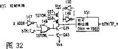
图32为示出图30A所示的电路中的HIT控制电路的具体配置示例的电路图。Fig. 32 is a circuit diagram showing a specific configuration example of the HIT control circuit in the circuit shown in Fig. 30A.
图33为示出图30A所示的电路中的行译码器的具体配置示例的电路图。Fig. 33 is a circuit diagram showing a specific configuration example of a row decoder in the circuit shown in Fig. 30A.
图34为用于说明根据本发明的第五实施例的半导体存储器件的配置示例的框图。FIG. 34 is a block diagram for explaining a configuration example of a semiconductor memory device according to a fifth embodiment of the present invention.
图35为用于说明在图34中示出的半导体存储器件中包含字线驱动器,行译码器和阵列控制电路部分的配置示例的框图。FIG. 35 is a block diagram for explaining a configuration example including a word line driver, a row decoder, and an array control circuit section in the semiconductor memory device shown in FIG. 34 .
图36为示出根据第五实施例的半导体存储器件中的行译码器和字线驱动器的抽出部分的具体配置的电路图。FIG. 36 is a circuit diagram showing a specific configuration of an extraction portion of a row decoder and a word line driver in a semiconductor memory device according to a fifth embodiment.
图37为用于说明根据第五实施例的半导体存储器件中的操作的时序图。FIG. 37 is a timing chart for explaining operations in the semiconductor memory device according to the fifth embodiment.
图38为用于说明根据第五实施例的半导体存储器件中的操作的时序图。FIG. 38 is a timing chart for explaining operations in the semiconductor memory device according to the fifth embodiment.
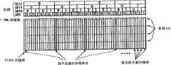
图39为示出在栈式字线测试模式中两个字线同时启用时的存储体的状态的示意图。FIG. 39 is a diagram illustrating the state of a memory bank when two word lines are simultaneously enabled in a stacked word line test mode.
图40为示出在栈式字线测试模式中八个字线同时启用时的存储体的状态的示意图。FIG. 40 is a diagram illustrating the state of a memory bank when eight word lines are simultaneously enabled in a stacked word line test mode.
图41A为示出在正常操作中列地址AR_ADD,信号X_ADD,信号XBLKP和存储块阵列号之间的对应关系的示意图。FIG. 41A is a diagram showing the correspondence between the column address AR_ADD, the signal X_ADD, the signal XBLKP, and the memory block array number in normal operation.
图41B为示出在四倍字线测试模式中(在TM1011MUSI进入时)列地址AR_ARD,信号X_ADD,信号XBLKB和存储块阵列号之间的对应关系的示意图。FIG. 41B is a schematic diagram showing the correspondence between the column address AR_ARD, the signal X_ADD, the signal XBLKB and the memory block array number in the quadruple word line test mode (when TM1011MUSI enters).
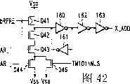
图42为用于说明用来实现四倍字线测试模式的X预译码器的配置的电路图。FIG. 42 is a circuit diagram for explaining the configuration of an X pre-decoder used to implement a quadruple word line test mode.
图43为用于说明用来实现四倍字线测试模式的X预译码器的安排的示例图。FIG. 43 is an exemplary diagram for explaining the arrangement of an X predecoder for realizing a quadruple word line test mode.
图44为用于说明用来实现四倍字线测试模式的X预译码器的配置的电路图。FIG. 44 is a circuit diagram for explaining the configuration of an X predecoder used to implement a quad word line test mode.
图45为示出行译码器和字线驱动器的抽出部分的框图,用于说明根据本发明的第七实施例的半导体存储器件。FIG. 45 is a block diagram showing extracted portions of a row decoder and a word line driver for explaining a semiconductor memory device according to a seventh embodiment of the present invention.
图46为示出TRDE控制电路的配置示例的电路图。FIG. 46 is a circuit diagram showing a configuration example of a TRDE control circuit.
图47为示出图45所示的电路中的bRDOUT和锁存电路配置示例的电路图。FIG. 47 is a circuit diagram showing a configuration example of bRDOUT and a latch circuit in the circuit shown in FIG. 45 .
图48为示出图45所示的电路中的X译码器的配置示例的电路图。FIG. 48 is a circuit diagram showing a configuration example of an X decoder in the circuit shown in FIG. 45 .
图49为示出图45所示的电路中的字线的配置示例的框图。FIG. 49 is a block diagram showing a configuration example of word lines in the circuit shown in FIG. 45 .
图50为示出图49所示的每个字线驱动器的配置示例的电路图。FIG. 50 is a circuit diagram showing a configuration example of each word line driver shown in FIG. 49 .
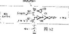
图51为冗余系统的示意图,用于说明根据本发明的第八实施例的半导体存储器件。FIG. 51 is a schematic diagram of a redundant system for explaining a semiconductor memory device according to an eighth embodiment of the present invention.
图52为示出图51所示的电路中的熔丝锁存电路的具体配置示例的电路图。FIG. 52 is a circuit diagram showing a specific configuration example of a fuse latch circuit in the circuit shown in FIG. 51 .
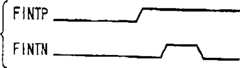
图53为用于说明熔丝启动信号的时序图。Fig. 53 is a timing chart for explaining a fuse enable signal.
图54为具有测试在熔丝熔断之前是否至少有一个冗余元件是有缺陷的元件的冗余测试功能的冗余系统的示意图。FIG. 54 is a schematic diagram of a redundancy system having a redundancy test function of testing whether at least one redundant element is a defective element before a fuse is blown.
图55为示出由存储器单元阵列抽出并且其中每个读出放大器是由邻接存储块中的位线对共用的两个存储块的示意图。Fig. 55 is a schematic diagram showing two memory blocks extracted from a memory cell array and in which each sense amplifier is shared by a pair of bit lines in adjacent memory blocks.
图56为示出熔丝设置选择信号生成电路的配置示例的电路图。FIG. 56 is a circuit diagram showing a configuration example of a fuse setting selection signal generating circuit.
图57为示出熔丝设置选择电路的配置示例的电路图。FIG. 57 is a circuit diagram showing a configuration example of a fuse setting selection circuit.
图58为用于说明在根据第八实施例的半导体存储器件中确定修补区的方法的示意图。FIG. 58 is a schematic diagram for explaining a method of determining a repair area in the semiconductor memory device according to the eighth embodiment.
图59为用于说明独立数据项可同时在分层数据线配置中的存储器单元阵列中读/写的字线数的示意图。FIG. 59 is a schematic diagram illustrating the number of word lines on which individual data items can be simultaneously read/written in a memory cell array in a hierarchical data line configuration.
图60为用于说明由在首先启用的字线上的非稳态单元造成的数据破坏。Figure 60 is used to illustrate data corruption caused by astable cells on the first enabled word line.
图61为用于说明根据本发明的第九实施例的示意图。而Fig. 61 is a schematic diagram for explaining a ninth embodiment according to the present invention. and
图62为示出沟道单元的1/2间距单元阵列的配置图形的示意图。FIG. 62 is a schematic diagram showing a configuration pattern of a 1/2 pitch cell array of trench cells.
具体实施方式第一实施例DETAILED DESCRIPTION OF THE PREFERRED EMBODIMENT
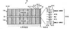
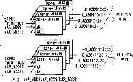
图1示出利用集中冗余系统的64-Mbit存储器单元阵列,用于说明根据本发明第一实施例的半导体存储器件的轮廓。如图1所示,存储器单元阵列11是分割为多个阵列11-0至11-31,并且设置有阵列控制电路段12和控制信号连线段13用来将阵列11-0至11-31中的每个分割为两个存储块。于是就形成一个32位正常单元阵列部件(32Mb UNIT(L))11A和32位正常单元阵列部件(32Mb UNIT(R))11B。FIG. 1 shows a 64-Mbit memory cell array utilizing a centralized redundancy system for explaining the outline of a semiconductor memory device according to a first embodiment of the present invention. As shown in Figure 1, the
另外,除了正常使用的正常单元阵列(称其为正常单元阵列)11之外,还提供一个存储器单元阵列(包含多个行冗余元件并且在此示例称为备用单元阵列)14专门用于行冗余替换,并且当正常单元阵列中的11-0至11-31中至少一个变成有缺陷时,缺陷阵列中的该缺陷元件(缺陷字线)通过使用备用单元阵列14中的行冗余元件被替换而得到修补(补偿)。In addition, in addition to a normal cell array (referred to as a normal cell array) 11 for normal use, a memory cell array (containing a plurality of row redundant elements and referred to as a spare cell array in this example) 14 dedicated to a row is provided. Redundant replacement, and when at least one of 11-0 to 11-31 in the normal cell array becomes defective, the defective element (defective word line) in the defective array is redundantly replaced by using the row in the
在此场合,为了缩短测试时间,在功能测试时同时启用8个阵列,比如同时启用阵列11-3,11-7...,11-31,图中以阴影线表示。In this case, in order to shorten the test time, 8 arrays are simultaneously enabled during functional testing, for example, the arrays 11-3, 11-7..., 11-31 are simultaneously enabled, which are indicated by hatching in the figure.
在控制信号连线段13中有9个控制信号线13-1至11-9。信号线13-1用于确定字线的启用和停用的定时的字线状态信号WLE。信号线13-2,13-3用于指示出现冗余替换的信号HITL,HITR。信号线13-4,13-5,13-6用于指定在正常单元阵列部件11A中包含缺陷字线的存储卡的地址DWAL0至DWAL2。信号线13-7,13-8,13-9用于指定在正常单元阵列部件11B中包含缺陷字线的存储卡的地址DWAR0至DWAR2。In the control
当缺陷阵列中的缺陷元件(缺陷字线)被备用单元阵列14中的行冗余元件(备用字线)替换时,信号HITL,HITR上升并且指示此时有待替换的具有缺陷元件的缺陷储存块的地址DWAL0至DWAL2和地址DWAR0至DWAR2发生改变。于是,执行操作以防止在出现与地址DWAL0至DWAL2和地址DWAR0至DWAR2符合的位置上的存储块接收字线状态信号(启用信号)WLE。When the defective element (defective word line) in the defect array is replaced by the row redundant element (spare word line) in the
图2示出在正常单元阵列11中的地址DWAL0至DWAL2和地址DWAR0至DWAR2的地址分配的示例。在正常单元阵列部件11A中的存储块为地址DWAL0至DWAL2所选定,而在正常单元阵列部件11B中的存储块为地址DWAR0至DWAR2所选定。比如,在时间DWAR0=1,DWAR1=1和DWAR2=1时,位于左上部分的存储块11B-28至11B-31被选定并在时间DWAR0=0,DWAR1=0和DWAR2=0时,位于右上部分的存储块11B-0至11B-0被选定。FIG. 2 shows an example of address allocation of addresses DWAL0 to DWAL2 and addresses DWAR0 to DWAR2 in the
图3为特别示出在图1所示的半导体存储器件中的阵列控制电路段12和控制信号连线段13的抽出部分(在正常单元阵列部件11A一侧)的电路略图。指示出现冗余替换的信号HITL和具有指示存储块11A-0至11A-31中的一个有待替换的信息的信号(地址)DWAL0至DWAL2由冗余控制信号输出电路20提供给信号线13-2,13-4,13-5,13-6。另外,对应于相应的各存储块的阵列控制电路12-0至12-31连接到信号线13-2,13-4,13-5,13-6。3 is a schematic circuit diagram showing in particular the extracted portion (on the side of the normal
阵列控制电路12-0由反相器21-0,22-0,23-0,24-0和25-0配置。地址DWAL0至DWAL2分别提供给反相器21-0,22-0,23-0对输入端子以形成其反相信号bDWAL0至bDWAL2。信号bDWAL0至bDWAL2和信号HITL提供给NAND门25-0。NAND门25-0对输出信号由反相器24-0反相以形成指示相应的存储块是否停用的信号DWAL0。The array control circuit 12-0 is configured by inverters 21-0, 22-0, 23-0, 24-0 and 25-0. The addresses DWAL0 to DWAL2 are respectively supplied to the pair of input terminals of the inverters 21-0, 22-0, 23-0 to form their inverted signals bDWAL0 to bDWAL2. The signals bDWAL0 to bDWAL2 and the signal HITL are supplied to the NAND gate 25-0. The output signal of NAND gate 25-0 is inverted by inverter 24-0 to form signal DWAL0 indicating whether the corresponding memory block is disabled.
阵列控制电路段12-1至12-31的配置方式与上述相同,并且分别形成指示相应的存储块是否停用的信号DWALA1至DWALA31。The array control circuit sections 12-1 to 12-31 are configured in the same manner as above, and respectively form signals DWALA1 to DWALA31 indicating whether the corresponding memory blocks are disabled.
另外,正常单元阵列11B的配置与正常单元阵列11A的配置相同,并且用于字线状态信号WLE的信号线13-1由正常单元阵列11A和11B共用。In addition, the configuration of the
图4A和4B示出在图1至图3中示出的半导体存储器件中的冗余替换操作,在图1至图3中示出的正常单元阵列11A为示例。如果在集中冗余系统中提供一个备用单元阵列,则在正常单元阵列11A中的多个存储块中的字线同时启用的场合当只有字线中的一个变成缺陷字线时就可以执行冗余替换操作。此时,执行控制操作以选择备用单元阵列14的备用字线来替换缺陷字线并且不选择正常单元阵列中的有待替换的字线。4A and 4B illustrate redundant replacement operations in the semiconductor memory device shown in FIGS. 1 to 3 , taking the
即如图4B的时序图所示,指示出现冗余替换的信号HITL首先上升到“H”电平并设置指示有待替换的存储块的位置的地址DWAL0至DWAL2。在此状态,如信号WLE上升到“H”电平,则正常单元阵列的有待替换的字线WL_b设置为非选定状态(WL停用)并且备用单元阵列14的备用字线WL_a上升到“H”电平并设置为选定状态。之后,如信号WLE下降到“L”电平,则备用单元阵列14的备用字线WL_a下降到“L”电平并设置为非选定状态。That is, as shown in the timing chart of FIG. 4B, the signal HITL indicating occurrence of redundant replacement first rises to "H" level and sets addresses DWAL0 to DWAL2 indicating the location of the memory block to be replaced. In this state, if the signal WLE rises to "H" level, the word line WL_b to be replaced of the normal cell array is set to a non-selected state (WL is disabled) and the spare word line WL_a of the
如上所述,在根据本发明的第一实施例的半导体存储器件中,在正常单元阵列11A,11B中的多个(2n:n是自然数)元件(存储块)同时启用,并且如果多个元件中至少有一个是有缺陷的,则执行只是选择性地替换缺陷元件的控制操作,操作是利用一个用来确定行冗余替换是否进行的信号(HITL/HITR)及n个用来确定要在行冗余替换时同时启用的多个元件中的一个的信号(地址DWAL,DWAR)。As described above, in the semiconductor memory device according to the first embodiment of the present invention, a plurality of (2n : n is a natural number) elements (memory blocks) in the
还有,还可能考虑一种改型,其中备用单元中的冗余元件是用来替换正常单元阵列中的任何一个缺陷元件(缺陷字线)。Also, it is also possible to consider a modification in which a redundant cell in a spare cell is used to replace any defective cell (defective word line) in a normal cell array.
即对于与有待同时启用的元件数(存储块)相对应的数的存储块的启用信号并无要求,使用的是通过统一启用信号和停用信号而得到的字线状态信号WLE,并且当字线状态信号WLE上升时启用地址与缺陷字线相应的地址符合的字线,而当字线状态信号WLE下降时停用。另外,在行冗余替换过程中,使用的是包含指示有待替换的存储块中的一个的信息的地址(DWALn,DWARn)及指示选择冗余替换的信号(HITL,HITR)。除此之外,包含指示有待替换的存储块中的一个的信息的地址DWALn,DWARn在存储块的阵列控制电路中本地译码。That is, there is no requirement for the enable signal of the storage blocks corresponding to the number of elements (storage blocks) to be activated at the same time, and the word line state signal WLE obtained by unifying the enable signal and the disable signal is used, and when the word The word line whose address matches the address corresponding to the defective word line is enabled when the line state signal WLE rises, and is disabled when the word line state signal WLE falls. Also, in the row redundancy replacement process, addresses (DWALn, DWARn) including information indicating one of the memory blocks to be replaced and signals (HITL, HITR) indicating selection of redundancy replacement are used. In addition, the address DWALn, DWARn, containing information indicating one of the memory blocks to be replaced, is decoded locally in the array control circuit of the memory block.
因此,采用上述配置时,由于多个元件(存储块)可同时启用,所以测试时间可以缩短,并且由于包含冗余信息的信号可本地译码,有待同时启用的存储块数易于增加,并且测试时间可缩短。另外,控制信号线的数目的增加可压缩到最小,并且,比如,在需要同时启用8个存储块时给信号WLE,HITL,HITR和地址DWAL0至DWAL2及DWAR0至DWA2提供9根信号线就已足够。即如果提供2n个有待同时启用的存储块,使用n个地址DWALn,DWARn就已足够。这样,连线数的增加可压缩,并且通过减小芯片地大小可降低成本。第二实施例Therefore, with the above configuration, since a plurality of elements (memory blocks) can be activated simultaneously, the test time can be shortened, and since signals containing redundant information can be decoded locally, the number of memory blocks to be simultaneously activated is easy to increase, and the test The time can be shortened. In addition, the increase in the number of control signal lines can be compressed to a minimum, and, for example, it is enough to provide 9 signal lines for signals WLE, HITL, HITR and addresses DWAL0 to DWAL2 and DWAR0 to DWA2 when 8 memory blocks need to be enabled simultaneously. enough. That is, if 2n memory blocks to be enabled simultaneously are provided, it is sufficient to use n addresses DWALn, DWARn. Thus, the increase in the number of connections can be suppressed, and the cost can be reduced by reducing the chip size. second embodiment
图5至12说明根据本发明的第二实施例的半导体存储器件,其中企图通过使用一种栈式字线测试模式(栈式WL测试模式)来减少测试时间。5 to 12 illustrate a semiconductor memory device according to a second embodiment of the present invention in which reduction in test time is attempted by using a stacked word line test mode (stacked WL test mode).
在此场合,栈式字线测试模式(也称为复式WL测试模式)是这样一种测试模式,其中通过同时启用具有相应延时代字线将N个或更多个字线设置为启用态,条件是如果在正常读/写操作时存储器单元阵列(或单元阵列部件)中有待同时启用的字线数是,比如,N。In this case, a stacked word line test mode (also referred to as a multiple WL test mode) is a test mode in which N or more word lines are set to an enabled state by simultaneously enabling word lines with corresponding delays, The condition is if the number of word lines to be simultaneously enabled in the memory cell array (or cell array section) is, for example, N during normal read/write operations.
在上述的栈式字线测试模式中,为了保证数据可以从存储单元中读出,对待选的字线的数目有某些限制。即可对与其相关的某些位线对和一个读出放大器(将其统称为存储块)启用的字线的数目只能是1。另外,当按共用方式使用读出放大器或由一个邻接的存储块共享(共享读出放大器)时,则按共用方式使用该读出放大器的存储块中只有一个可选该字线。换言之,在具有N个存储块的存储器单元阵列(或单元阵列部件)中最多只有N/2个字线可选。In the above-mentioned stacked word line test mode, in order to ensure that data can be read from the memory cells, there are certain restrictions on the number of word lines to be selected. That is, the number of word lines enabled for certain bit line pairs and a sense amplifier (collectively referred to as a memory block) associated therewith can only be one. In addition, when the sense amplifier is used in common or is shared by an adjacent memory block (shared sense amplifier), only one of the memory blocks using the sense amplifier in common can select the word line. In other words, there are at most N/2 word lines available in a memory cell array (or cell array unit) with N memory blocks.
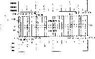
下面参考图5至10说明实现栈式字线测试模式的共享读出放大器系统的半导体存储器件的配置。图5示出由多个单元阵列部件配置的存储体的一部分,一个单元阵列部件30由32个存储块配置(32个存储块/部件),并且现用存储块31AB和休眠存储块31SB是交替配置的。行译码段33,字线(WL)驱动器段34和阵列控制电路35T,35B分别配置于与相应的存储块31AB,31SB邻接的位置。存储块(阵列号0至31)由分割为两段各8k的行并由行地址AR_ADD9至AR_ADD12选择,如图所示。The configuration of the semiconductor memory device realizing the shared sense amplifier system of the stacked word line test mode will be described below with reference to FIGS. 5 to 10 . 5 shows a part of a memory bank configured by a plurality of cell array parts, one
更具体言之,现用读出放大器36AB是设置于每个现用存储块31SB的两边并且休眠读出放大器36SS设置成为与每个休眠存储块31SB相邻接。另外,行译码段33和字线(WL)驱动器段34设置成为与每个存储块相邻接,并且第一阵列控制电路(上面的)35T和第二阵列控制电路(下面的)35B设置成为与相应的现用读出放大器36AS相邻接。More specifically, active sense amplifiers 36AB are disposed on both sides of each active memory block 31SB and sleep sense amplifiers 36SS are disposed adjacent to each sleep memory block 31SB. In addition, a
虽然图中未示出,在存储单元阵列(或称单元阵列部件)30中包含列译码器,冗余控制电路,再驱动器,X预译码器和存储体控制电路。Although not shown in the figure, a column decoder, a redundancy control circuit, a redriver, an X pre-decoder and a bank control circuit are included in the memory cell array (or cell array unit) 30 .
图6为示出在存储器单元阵列中的存储块31,读出放大器36,行译码器33,字线(WL)驱动器段34和阵列控制电路35T(35_n(t)),35B(35_n(b))从存储单元阵列(或单元阵列部件)30的抽出部分的具体配置的示例。存储块31_n和读出放大器36_n(t),36_n(b)经位线对BL/bBL相互连接。与存储块31_n连接的字线WL由设置于字线(WL)驱动器段34上的驱动器34A驱动。字线(WL)驱动器段34A接收从行译码器33A发出的译码信号输出和从WLDV驱动器38发出的输出以控制字线的驱动和复位。行译码器33A接收从外围电路和再驱动器37发出的地址信号XAdd和从TWLOFF控制电路39发出的信号TWLOFF以中断字线的驱动。TWLOFF控制电路39接收从外围电路和再驱动器37发出的信号bWLOFF以中断字线的驱动并接收从块选择器43输出的块选择信号BLKSEL。Fig. 6 shows
读出放大器36_n(t),36_n(b)分别与第一和第二阵列控制电路35_n(t),35_n(b)。第一和第二阵列控制电路35_n(t),35_n(b)每个都配置成为包含WLDV驱动器38,N/PSET驱动器40,读出放大器(SA)控制电路41,TWLON控制电路42,块选择器43等等。读出放大器36_n(t/b)的启用停用由N/PSET驱动器40输出的信号N/PSET控制。N/PSET驱动器40接收读出放大器(SA)控制电路41的输出信号SVLD和从外围电路及再驱动器37发出的读出放大器启用信号SAE。另外,WLDV驱动器38接收从TWLOFF控制电路39发出的信号TWLOFF和从TWLON控制电路42发出的信号TWLON。驱动字线由信号TWLON确定,并且字线驱动的中断由信号TWLOOF确定。TWLON控制电路42接收外围电路和再驱动器37发出的信号bWLON。另外,SA控制电路41接收从外围电路和再驱动器37输出的信号bWLON,从块选择器43输出的信号BLKSEL和从邻接的下一个块选择器43输出的信号BLKSEL。块选择器43接收从外围电路和再驱动器37输出的信号XAdd。The sense amplifiers 36_n(t), 36_n(b) communicate with the first and second array control circuits 35_n(t), 35_n(b) respectively. The first and second array control circuits 35_n(t), 35_n(b) are each configured to include a
图7为示出从图6所示的电路中的外围电路和再驱动器37中抽出的X预译码器,冗余控制电路和再驱动器的配置示例的电路图。此电路的配置包含冗余控制电路50,再驱动器51,bWLOFF锁存电路52,再驱动器53,SAE锁存电路54,再驱动器55,bRPRE锁存电路56,X预译码器57等等。FIG. 7 is a circuit diagram showing a configuration example of an X predecoder, a redundant control circuit and a redriver extracted from the peripheral circuits and
信号ARAdd供给冗余控制电路50,而由冗余控制电路50输出的信号bFWLON供给再驱动器51。信号bWLON由再驱动器51输出。The signal ARAdd is supplied to the
信号TMWLLTC和bRSTR输送给bWLOFF锁存电路52,bWLOFF锁存电路52的输出信号供给再驱动器53,而信号bWLOFF由再驱动器53输出。The signals TMWLLTC and bRSTR are supplied to a bWLOFF latch circuit 52, the output signal of the bWLOFF latch circuit 52 is supplied to a
另外,信号TMSALTC和QSAE供给SAE锁存电路54,而SAE锁存电路54的输出信号供给再驱动器55,信号SAE由再驱动器55输出。In addition, the signals TMSALTC and QSAE are supplied to the
信号bRSTR,TMSALTC和QSAE供给bRPRE锁存电路56,并且bRPRE锁存电路56的输出信号bRPRE和信号ARAdd供给X预译码器57,而信号XAdd是从X预译码器57输出的。Signals bRSTR, TMSALTC and QSAE are supplied to
图8为示出图7所示的电路中的bWLOFF锁存电路52的配置示例的电路图。bWLOFF锁存电路52的配置有反相器58至61和NAND门62。信号bRSTR,TMWLLTC分别供给反相器58和59的输入端子。反相器58,59的输出供给NAND门62并且NAND门62的输出信号是作为信号bWLOFF经反相器60,61输出。FIG. 8 is a circuit diagram showing a configuration example of the bWLOFF latch circuit 52 in the circuit shown in FIG. 7 . The bWLOFF latch circuit 52 is configured with
图9为示出图7所示的SAE锁存电路的配置示例的电路图。SAE锁存电路54由P沟道MOS晶体管Q1,Q2,N沟道MOS晶体管Q3和反相器63至66配置。MOS晶体管Q1至Q3的电流通路系串联于电源Vcc和地节点Vss之间。信号TMSALTC供给MOS晶体管Q1的栅极,而信号QSAE供给MOS晶体管Q2,Q3的栅极。MOS晶体管Q2和Q3的电流通路的连接节点连接到反相器63的输入端子。反相器63输入端子和输出端子分别连接到反相器64的输出端子和输入端子。另外,反相器63的输出端子连接到反相器65的输入端子,而反相器65的输出端子连接到反相器66的输入端子。信号SAE是由反相器66输出的。FIG. 9 is a circuit diagram showing a configuration example of the SAE latch circuit shown in FIG. 7 . The
图10A和图10B分别为示出图7所示的bRPRE锁存电路56和X预译码器57的配置示例的电路图。图7中示出的bRPRE锁存电路56的配置包含反相器67至69,NOR门70和NAND门71。信号TMSALTC经反相器67供给NAND门71的一个输入端子。信号QSAE和bRSTR供给NOR门70的输入端子,而NOR门70的一个输出信号供给NAND门71的另一个输入端子。NAND门71的一个输出信号经反相器68,69作为信号bRSTR输出。10A and 10B are circuit diagrams showing configuration examples of the
图10B中示出的X预译码器57的配置包含P沟道MOS晶体管Q4,N沟道MOS晶体管Q5至Q7和反相器72至75。MOS晶体管Q4至Q7的电流通路系串联于电源Vcc和地节点Vss之间。从bRPRE锁存电路56输出的信号bRSTR供给MOS晶体管Q4,Q5的栅极,一个地址信号AR_i供给MOS晶体管Q6的栅极,而一个地址信号AR_j供给MOS晶体管Q7的栅极。MOS晶体管Q4和Q5的电流通路的连接节点连接到反相器72的输入端子。反相器72的输入端子和输出端子分别连接到反相器73的输出端子和输入端子。另外,反相器72的输出端子连接到反相器74输入端子,而反相器74的输出端子连接到反相器75的输入端子。信号X_ADD是由反相器75的输出端子输出的。The configuration of the
信号X_ADD(XAdd)输入到WLDV驱动器38,行译码段33A和块选择器43。在8k行和32个存储块/部件的场合,一个信号X_ADD01(AR_ADD0,AR_ADD1)输入到WLD驱动器38,信号X_ADD23,45,678(AR_ADD2至AR_ADD8)输入到行译码段33A,而信号X_ADD910,1112(AR_ADD9至AR_ADD12)输入到块选择器43。8k字线利用地址X_ADD有选择地启用。The signal X_ADD (XAdd) is input to the
下面参考图11的时序图对栈式字线测试模式中的操作予以说明。如进入栈式字线测试模式(TM ENTRY),TMSALTC变成为“H”和TMWLLTC变成为“H”。对其响应为bWLOFF从“L”变为“H”,bRPRE从“L”变为“H”,且此状态一直保持不变直到操作脱离此测试模式。The operation in the stacked word line test mode will be described below with reference to the timing diagram of FIG. 11 . If entering the stacked word line test mode (TM ENTRY), TMSALTC becomes "H" and TMWLLTC becomes "H". In response to this, bWLOFF changes from "L" to "H", bRPRE changes from "L" to "H", and this state remains unchanged until the operation leaves this test mode.
首先,选择第一字线并且其电位设置为“H”电平(循环#1)。在此示例中,由于使用的是32个存储块/存储单元阵列(单元阵列部件),对于每个存储单元阵列(单元阵列部件)可选的字线数最多为16。因为在每个存储块中只有一个字线可选,用来对阵列(AR_ADD0至AR_ADD8)(指定阵列中的行)译码的行地址固定设置。因为在使用共享读出放大器的条件下16个存储块无需启用邻接存储块而进行选择,用来选择存储块的行地址AR_ADD10,AR_ADD11,AR_ADD12顺序相加并提取(行地址AR_ADD9固定设置)。First, the first word line is selected and its potential is set to "H" level (cycle #1). In this example, since 32 memory blocks/memory cell arrays (cell array section) are used, the number of word lines selectable for each memory cell array (cell array section) is 16 at most. Because only one word line is optional in each memory block, the row address used for decoding the array (AR_ADD0 to AR_ADD8) (designating the row in the array) is fixedly set. Because the 16 memory blocks do not need to enable adjacent memory blocks to select under the condition of using the shared sense amplifier, the row addresses AR_ADD10, AR_ADD11, and AR_ADD12 for selecting the memory block are sequentially added and extracted (the row address AR_ADD9 is fixedly set).
当接收到一个存储体现用命令BA时,一个信号bRSTR(内RAS)从“L”改变为“H”,提取的行地址传输到AR_ADD9,AR_ADD10,AR_ADD11,AR_ADD12以便启用地址X_ADD910_1,X_ADD1112_1。对启用的地址X_ADD910_0,X_ADD1112_0的响应是从块选择器43输出的信号BLKSE_0从“L”改变为“H”。响应这种改变,TWLOFF控制电路39将TWLOFF从“L”设置为“H”以便从预充电操作释放行译码段33A。结果,由先前启用的地址X_ADD23,X_ADD45,C_ADD678选定的行译码器所确定的字线驱动器34A被启用。When a memory bank command BA is received, a signal bRSTR (internal RAS) changes from "L" to "H", and the extracted row address is transferred to AR_ADD9, AR_ADD10, AR_ADD11, AR_ADD12 to enable addresses X_ADD910_1, X_ADD1112_1. The response to the enabled address X_ADD910_0, X_ADD1112_0 is that the signal BLKSE_0 output from the block selector 43 changes from "L" to "H". In response to this change, the
还有,提取的地址AR_ADD也输入到冗余控制电路50并与冗余信息进行比较。即输入地址AR_ADD和先前准备的冗余信息(比如由切断熔丝确定的地址信息)互相进行比较。结果,如未能取得符合,(无符合,以后称其为失败或冗余失败),则信号bFWLON变为“L”电平的脉冲。如取得符合(符合,以后称其为命中或冗余命中),则信号bFWLON保持为“上升到“H”电平。Also, the extracted address AR_ADD is also input to the
在冗余失败的场合,TWLON_0(b/t)从“L”变为“H”并且由信号X_ADD01_0确定的WLDV_0和WLRST_0分别从“L”变为“H”和从“H”变为“L”以响应信号bWLON的“L”电平脉冲。另外,先前启用的字线驱动器将字线WL_0从“L”设置为“H”来响应“H”的WLDV_0和“L”的WLRST_0以便将在存储单元中的编程数据传输到位线BL_0。In case of redundancy failure, TWLON_0(b/t) changes from "L" to "H" and WLDV_0 and WLRST_0 determined by signal X_ADD01_0 change from "L" to "H" and from "H" to "L" respectively ” in response to the “L” level pulse of signal bWLON. In addition, the previously enabled wordline driver sets wordline WL_0 from "L" to "H" in response to WLDV_0 of "H" and WLRST_0 of "L" to transfer program data in memory cells to bitline BL_0.
下面说明读出放大器36_n(t/b)的启用。当由信号BLKSEL_0选定的读出放大器控制电路41接收到“L”的bWLON时,则SAVLD_0(b/t)从“L”设置为“H”。当经过足够长的时间可以预期利用保障设置于外围电路段的电路的字线延时足以能使WL设置为“H”时,通过反相器55将QSAE从“L”设置为“H”。现在,因为TMSALTC保持为“H”,“H”的SAE保持不变直到操作脱离此测试模式。响应SAE从“L”变为“H”,N/PSET驱动器40将NSET_0(b/t)从“H”设置为“L”以启用读出放大器36_n(t/b)。由此,位线BL/bBL的读出操作就可利用读出放大器36_n(t/b)来执行。Next, activation of the sense amplifier 36_n(t/b) will be described. When the sense amplifier control circuit 41 selected by the signal BLKSEL_0 receives bWLON of "L", then SAVLD_0(b/t) is set from "L" to "H". QSAE is set from “L” to “H” through the
之后,当接收到存储体预充电命令PR时,bRSTR从“H”设置为“L”并且QSAE从“H”设置为“L”。在正常读/写操作中,bWLOFF从“H”设置为“L”并且选定的WL从“H”设置为“L”来响应“L”的bRSTR。另外,响应“L”的QSAE,将QSAE设置为“L”及NSET=“L”/bPSET=“H”以便停用读出放大器36_n(t/b)及均衡位线BL/bBL。After that, when the bank precharge command PR is received, bRSTR is set from "H" to "L" and QSAE is set from "H" to "L". In normal read/write operation, bWLOFF is set from “H” to “L” and the selected WL is set from “H” to “L” in response to a bRSTR of “L”. Also, in response to QSAE of "L", set QSAE to "L" and NSET = "L"/bPSET = "H" to disable sense amplifier 36_n(t/b) and equalize bit line BL/bBL.
然而,在此场合,因为如进入测试模式,“H”的bWLOFF/“H”的SAE一直保持,所以选择字线WL并设置为启用态,读出放大器36_n(t/b)设置为启用态,并且位线对BL/bBL的电位保持锁存。另外,因为bRPRE保持为“H”,所有选定的信号X_ADD保持为启用态(X_ADD未复位)。在其他场合,这些状态传输到与接收到正常操作的存储体预充电命令的状态相同的状态。However, in this case, since the bWLOFF of "H"/SAE of "H" is always maintained when entering the test mode, the word line WL is selected and set to an enabled state, and the sense amplifier 36_n(t/b) is set to an enabled state , and the potential of the bit line pair BL/bBL remains latched. Also, since bRPRE remains "H", all selected signals X_ADD remain enabled (X_ADD is not reset). On other occasions, these states transfer to the same state as the state upon receipt of the bank precharge command for normal operation.
之后,选择下一个字线WL的操作开始(循环#2)。与第一循环的场合类似,当接收到一个存储体现用命令BA时,提取一个新的行地址。信号bRSTR(内RAS)从“L”改变为“H”,提取的行地址传输到AR_ADD9,AR_ADD10,AR_ADD11,AR_ADD12以便启用地址X_ADD910_1,X_ADD1112_1。此时,在前一个循环启用的信号X_ADD910_0,X_ADD1112_0保持为启用态。之后,执行与第一循环同样的操作并且由选定的行译码器33A确定的字线驱动器34A被启用。另外,提取的行地址AR_ADD也输入到冗余控制电路并与冗余信息进行比较。After that, the operation of selecting the next word line WL starts (loop #2). Similar to the case of the first cycle, when a bank use command BA is received, a new row address is extracted. Signal bRSTR (internal RAS) changes from "L" to "H", and the extracted row address is transferred to AR_ADD9, AR_ADD10, AR_ADD11, AR_ADD12 to enable addresses X_ADD910_1, X_ADD1112_1. At this time, the signals X_ADD910_0 and X_ADD1112_0 that were enabled in the previous cycle remain enabled. After that, the same operation as the first loop is performed and the
在冗余失败的场合,TWLON_1(b/t)从“L”变为“H”,并且由信号X_ADD01_1确定的WLDV_1和WLRST_1分别从“L”变为“H”和从“H”变为“L”以响应信号bWLON“L”电平脉冲。另外,先前启用的字线驱动器34A将字线WL_1从“L”设置为“H”以响应“H”的WLDV_1和“L”的WLRST_1以便使在存储单元阵列31_n中编程的数据传输到位线BL_1。In case of redundancy failure, TWLON_1(b/t) changes from "L" to "H", and WLDV_1 and WLRST_1 determined by signal X_ADD01_1 change from "L" to "H" and from "H" to " L" in response to signal bWLON "L" level pulse. In addition, the previously enabled
读出放大器36_n(t/b)的启用操作在第一循环和第二循环及后续的循环中不同。该操作与第一循环相同直到由信号BLKSEL_1选定的读出放大器(SA)控制电路41接收到“L”的bWLON以便将SAVLD_1(b/t)从“L”设置为“H”。在此场合,因为SAE保持为“H”,N/PSET驱动器40立即将NSET_1(b/t)从“L”设置为“H”并将bPSET_1(b/t)从“H”设置为“L”以响应“H”的SAVLD_1(b/t)。由此,因为读出放大器36_n(t/b)的启用是在字线WL_1启用之前以便足以将存储单元阵列31_n中的数据传输到位线BL_1并且位线的读出放大操作利用未定数据执行,所以在位线WL_1中编程的数据可能被破坏而无法保证正确的操作。The enable operation of the sense amplifier 36_n(t/b) is different in the first cycle and the second and subsequent cycles. The operation is the same as the first cycle until the sense amplifier (SA) control circuit 41 selected by signal BLKSEL_1 receives bWLON of "L" to set SAVLD_1(b/t) from "L" to "H". In this case, since SAE remains "H", the N/
此后,所有的启用字线返回到预充电状态。如接收到引起操作脱离栈式字线测试模式的命令,就将TMSALTC从“H”设置为“L”,将TMWLLTC从“H”设置为“L”。响应这种改变,bWLOFF从“H”设置为“L”和bRPRE从“H”设置为“L”以便使所有在测试模式中启用的位线和字线返回到预充电状态。但是,因为将WL从“H”设置为“L”对操作和均衡位线的操作是同时开始的,位线均衡操作的开始是在字线电位降低到足够低的电位(存储单元的晶体管彻底关断)之前。因此,存储单元阵列31_n的数据不能得到保证。Thereafter, all enabled word lines return to the precharged state. TMSALTC is set from "H" to "L" and TMWLLTC is set from "H" to "L" if a command is received that causes operation to exit the stacked word line test mode. In response to this change, bWLOFF is set from "H" to "L" and bRPRE is set from "H" to "L" to return all bit lines and word lines enabled in test mode to the precharge state. However, since setting WL from "H" to "L" starts simultaneously with the operation of equalizing the bit line, the equalization operation of the bit line starts when the potential of the word line is lowered to a sufficiently low potential (the transistor of the memory cell is fully before shutdown). Therefore, the data of the memory cell array 31_n cannot be guaranteed.
下面(参考图12的时序图)考虑冗余命中的场合。在此场合,说明是在假定冗余命中是在第二循环中发生。执行与冗余失败同样的操作直到完成进入(TM ENTRY)测试模式及执行循环#1的存储体启用过程和存储体预充电操作。Next (refer to the timing diagram of FIG. 12 ) consider the case of a redundant hit. In this case, the description assumes that the redundant hit occurs in the second cycle. Perform the same operation as for redundancy failure until the completion of entering (TM ENTRY) test mode and executing the bank enable process and bank precharge operation of
在第二循环中开始选择下一个字线的操作。与第一循环的场合类似,当接收到一个存储体现用命令BA时,提取一个新的行地址(AR_ADD)。之后,执行与第一循环中同样的操作以启用由行译码器33A选定的字线驱动器34A。之后,提取的行地址AR_ADD也输入到冗余控制电路并与冗余信息进行比较。在冗余命中的场合,因为信号bWLON由冗余控制电路保持为“H”电平状态,TWLON_1(b/t)维持为“L”和由信号X_ADD01_1确定的WLDV_1及WLRST_1分别保持为“L”和“H”。由此,先前启用的字线驱动器34A将字线WL_1设置为“L”响应“L”的WLDV_1和“H”的WLRST_1以便维持停用状态。The operation of selecting the next word line starts in the second cycle. Similar to the case of the first cycle, when a bank use command BA is received, a new row address (AR_ADD) is fetched. After that, the same operation as in the first loop is performed to enable the
读出放大器36_n(t/b)的启用操作在失败和命中的场合不同。因为信号bWLON在冗余命中时设置为“H”,由信号BLKSEL_1选定的读出放大器控制电路41继续输出“L”的SAVLD_1(b/t)。这样,SAE保持为“H”,因为TMSALTC设置为“H”,但N/PSET驱动器40设置NSET_1(b/t)为“L”并设置bPSET_1(b/t)为“H”以响应“L”的SAVLD_1(b/t)以便使读出放大器36_n(t/b)将不被启用。操作与正常冗余命中时相同。即执行所希望的操作。The enable operation of the sense amplifier 36_n(t/b) is different in case of a fail and a hit. Since the signal bWLON is set to "H" at the redundant hit, the sense amplifier control circuit 41 selected by the signal BLKSEL_1 continues to output SAVLD_1(b/t) of "L". Thus, SAE remains "H" because TMSALTC is set to "H", but N/
在第三循环中(循环#3)开始选择下一个字线的操作。与第一和第二循环的场合类似,当接收到一个存储体现用命令BA时,提取一个新的行地址(AR_ADD)。于是,由新选定的行译码器确定的字线驱动器34A由与与第一和第二循环中的同样的操作启用。之后,提取的行地址AR_ADD也输入到冗余控制电路与冗余信息进行比较。In the third cycle (cycle #3), the operation of selecting the next word line starts. Similar to the cases of the first and second loops, when a bank use command BA is received, a new row address (AR_ADD) is fetched. Then, the
下面考虑冗余失败的场合。与第一循环的场合相同,TWLON_2(b/t)从“L”变为“H”,并且由信号X_ADD01_2确定的WLDV_2和WLRST_2分别从“L”变为“H”和从“H”变为“L”以响应信号bWLON的“L”电平脉冲。另外,先前启用的字线驱动器将字线WL_2从“L”设置为“H”以响应“H”的WLDV_2和“L”的WLRST_2以便使在存储单元中编程的数据传输到位线。在此循环中选定的字线就被启用。Consider the case where redundancy fails. Same as the case of the first cycle, TWLON_2(b/t) changes from "L" to "H", and WLDV_2 and WLRST_2 determined by the signal X_ADD01_2 change from "L" to "H" and from "H" to "L" in response to the "L" level pulse of signal bWLON. In addition, the previously enabled word line driver sets word line WL_2 from "L" to "H" in response to WLDV_2 of "H" and WLRST_2 of "L" in order to transfer the data programmed in the memory cell to the bit line. The word line selected during this cycle is enabled.
在此场合,应注意在第二循环中冗余命中的字线。即使是在第二循环中命中的行译码器和阵列控制电路的状态是设置为与第三循环同样的状态(失败),所有曾经使用过的信号X_ADD继续保持。即在第三循环中,所有在第二循环中用作访问的信号X_ADD910_1,X_ADD1112_1保持为启用状态。另外,BLKSEL_1保持于块选择器43中。因为bWLOFF设置为“H”,保持“H”的bTWLOFF_1的状态并启用由行译码器33A选定的字线驱动器34A的状态继续维持。此时,如在第三循环中输出“L”的bWLON脉冲,则输出在第二循环中选定的阵列控制电路中的“H”的TWLON_1(b/t)的脉冲,因为信号bWLON是存储器单元阵列(单元阵列部件)中的全局信号。响应此脉冲,在第二循环中设置为停用的信号WLDV_1被启用并且出现原来本不该命中和选定的字线被选定的可能性。In this case, attention should be paid to redundantly hit word lines in the second cycle. Even if the state of the row decoder and array control circuit hit in the second cycle is set to the same state (failure) as the third cycle, all the signals X_ADD that have been used continue to be maintained. That is, in the third cycle, all the signals X_ADD910_1 , X_ADD1112_1 used for access in the second cycle remain enabled. In addition, BLKSEL_1 is held in the block selector 43 . Since bWLOFF is set to "H", the state of bTWLOFF_1 that remains "H" and enables the
即根据第二实施例的半导体存储器件执行一种所希望的操作,其中字线/读出放大器在冗余命中循环中被停用,但在下一个和后续的循环中,会出现这样一种可能性,即在此循环中选定的读出放大器和字线被启用并且先前命中和停用的字线和读出放大器将被启用,因此在这一条件下不能保证正确的操作。第三实施例That is, the semiconductor memory device according to the second embodiment performs a desired operation in which the word line/sense amplifier is disabled in the redundant hit cycle, but in the next and subsequent cycles, there is a possibility that property, that is, the selected sense amplifier and word line are enabled in this cycle and the previously hit and disabled word line and sense amplifier will be enabled, so correct operation is not guaranteed under this condition. third embodiment
在第二实施例中,对于在第二和后续的循环中启用的字线保持冗余修补信息和从存储器单元读出数据(位线读出)的操作在多个字线可以以相应的延时设置为共同选定态的测试模式(栈式字线测试模式)中无法得到保证。因此,栈式字线测试模式在经过冗余修补(在熔丝熔断过程后)的产品中不能设置,且只有冗余修补前的产品或无需修补(替换)的合格产品可进行测试。In the second embodiment, operations to maintain redundant patch information and read data from memory cells (bit line read) for word lines enabled in the second and subsequent cycles can be performed on multiple word lines with corresponding delays. It cannot be guaranteed in the test mode (stacked word line test mode) which is set to the common selected state at the time. Therefore, the stacked word line test mode cannot be set in products that have undergone redundancy repair (after the fuse blowing process), and only products before redundancy repair or qualified products that do not need repair (replacement) can be tested.
在第三实施例中,于在第二和后续的循环中启用的字线的存储器单元的读出操作(位线读出操作)和保持冗余信息的操作可得到保证,并且经过冗余修补的产品中的存储器单元的数据可得到保证。不过,对每个存储块启用的字线数最多为1。In the third embodiment, the read operation (bit line read operation) of the memory cells of the word line enabled in the second and subsequent cycles and the operation of maintaining redundant information can be guaranteed, and after redundancy repair The data of the memory cells in the product can be guaranteed. However, the number of word lines enabled for each memory block is at most one.
图13至27说明根据本发明的第三实施例的半导体存储器件。图13为示出配置有多个存储器单元的存储体并基本上示出与图5中示出的第二实施例相同的配置。13 to 27 illustrate a semiconductor memory device according to a third embodiment of the present invention. FIG. 13 is a diagram showing a bank configured with a plurality of memory cells and basically shows the same configuration as the second embodiment shown in FIG. 5 .
即一个存储器单元阵列(或单元阵列部件)30配置有交叉配置的32个存储块(32个存储块/部件)和现用存储块31AB及休眠存储块31SB。行译码段33,字线(WL)驱动器段34和阵列控制电路35T,35B配置于与存储块邻接的位置。存储块(阵列号No.0至31)分割为各为8k的两段并由行地址AR_ADD9至AR_ADD12选择,如图中所示。That is, one memory cell array (or cell array unit) 30 is configured with 32 memory blocks (32 memory blocks/unit) interleaved, active memory block 31AB, and sleep memory block 31SB. The
更具体言之,现用读出放大器36AS是设置于每个现用存储块31AB的两边,并且休眠读出放大器36SS设置为与每个休眠存储块31SB相邻接。另外,行译码段33和字线驱动器段34设置为与每个存储块邻接,并且第一阵列控制电路(上面的)35T和第二阵列控制电路(下面的)35B设置成为与相应的现用读出放大器36AS相邻接。More specifically, active sense amplifiers 36AS are disposed on both sides of each active memory block 31AB, and sleep sense amplifiers 36SS are disposed adjacent to each sleep memory block 31SB. In addition, a
虽然图中未示出,在存储单元阵列(或称单元阵列部件)30中包含列译码器,冗余控制电路,再驱动器,X预译码器和存储体控制电路。Although not shown in the figure, a column decoder, a redundancy control circuit, a redriver, an X pre-decoder and a bank control circuit are included in the memory cell array (or cell array unit) 30 .
图14为示出从存储器单元阵列(单元阵列部件)30中抽出的存储器单元31_n,读出放大器36_n(t),36_n(b),行译码段33,字线驱动器34和阵列控制电路35T(35_n(t)),35B(35_n(b))的具体配置示例的电路图。存储单元阵列31_n和读出放大器36_n(t),36_n(b)通过位线对BL/bBL互相连接。与存储块31_n相连接的字线WL_n由字线驱动器34A驱动。字线驱动器34A接收从行译码器33A发出的译码信号输出和从WLDV驱动器38输出的信号WLDV_n/WLRST_n以控制字线的驱动和复位。行译码器33A接收从外围电路和再驱动器37发出的地址信号XAdd和TRDE锁存电路44的锁存输出TRDE_n。TRDE锁存电路44接收从外围电路和再驱动器37发出的信号TSTCWL,WLE,从相应的阵列控制电路的块选择器43发出的信号XBLKP_n和从后级阵列控制电路中的块选择器输出的信号XBLKP_n+1。Fig. 14 shows memory cell 31_n extracted from memory cell array (cell array part) 30, sense amplifier 36_n (t), 36_n (b),
读出放大器36_n(t),36_n(b)分别与第一和第二阵列控制电路35_n(t),35_n(b)。第一和第二阵列控制电路35_n(t),35_n(b)每个都配置成为包含WLDV驱动器38,N/PSET驱动器40,读出放大器(SA)锁存电路45,TWLON锁存电路46,命中控制电路47,锁存电路(BLKSEL锁存电路)48,块选择器43等等。读出放大器36_n(t/b)的启用停用由N/PSET驱动器40输出的信号N/PSET控制。N/PSET驱动器40接收读出放大器(SA)锁存电路45的锁存输出。SA锁存电路接收读出放大器(SA)控制电路41的输出信号SVLD_n和从外围电路及再驱动器37发出的信号bSAON,bSAOFF。The sense amplifiers 36_n(t), 36_n(b) communicate with the first and second array control circuits 35_n(t), 35_n(b) respectively. The first and second array control circuits 35_n(t), 35_n(b) are each configured to include a
另外,WLDV驱动器38接收从TWLON锁存电路46输出的信号TWLON_n和从外围电路和再驱动器37输出的信号XADD。SA控制电路41接收从相应的阵列控制电路中的锁存电路48输出的信号BLKSEL_n及从后级的阵列控制电路中的锁存电路48输出的信号BLKSEL_n+1。另外,TWLON锁存电路46接收从外围电路和再驱动器37输出的信号TSTCWL,WLE。In addition, the
命中控制电路47接收从外围电路和再驱动器37输出的信号HIT/DWA,从相应的阵列控制电路中的块选择器43输出的信号XBLKP_n及从后级的阵列控制电路中的块选择器43输出的信号XBLKP_n+1。另外,锁存电路48接收从外围电路和再驱动器37输出的信号bSAOFF和块选择器43的信号XBLKP_n。块选择器43接收从外围电路和再驱动器37输出的信号XAdd。The
就是说,根据第三实施例的半导体存储器件在每个阵列控制电路中包含一组在栈式字线测试模式中保持“H”的BLKSEL状态的BLKSEL锁存电路48,保持“H”的NSET/“L”的bPSET的读出放大器(SA)锁存电路45,具有在栈式字线测试模式中控制“L”/“H”的TWLON的功能和保持“H”电平状态的功能的TWLON锁存电路46,以及具有控制“L”/“H”的TRDE的功能和保持“H”电平的TRDE状态的功能的TRDE锁存电路。That is, the semiconductor memory device according to the third embodiment includes, in each array control circuit, a set of BLKSEL latch circuits 48 that hold the BLKSEL state of "H" in the stacked word line test mode, and NSET that hold "H". The sense amplifier (SA) latch circuit 45 of the bPSET of /"L" has the function of controlling the TWLON of "L"/"H" and the function of maintaining the "H" level state in the stacked word line test mode.
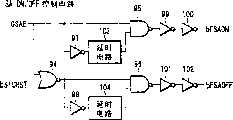
图15为示出图14所示的在外围电路和再驱动器37中的X预译码器,冗余控制电路和再驱动器的抽出部分的配置示例的电路图。此电路的配置包含冗余控制电路80,再驱动器81,冗余控制电路82,WLON/OFF控制电路83,再驱动器84,SAON/OFF控制电路(脉冲发生器)85,再驱动器86,bRPRE控制电路87,X预译码器88,X预译码器89,STCRST控制电路90等等。FIG. 15 is a circuit diagram showing a configuration example of an X pre-decoder, a redundancy control circuit, and an extraction portion of the
信号AR_ADD供给冗余控制电路80,而从冗余控制电路80输出的信号bFDWA和信号bFHIT供给再驱动器81。之后,信号HIT和DWA从再驱动器81输出。The signal AR_ADD is supplied to the
从冗余控制电路82输出的信号RADLTC和信号bFWJON供给WLON/OFF控制电路83。从WLON/OFF控制电路83输出的信号FWLE供给再驱动器84,而信号字线状态信号WLE从再驱动器84输出。The signal RADLTC and the signal bFWJON output from the
在第二实施例中信号WLE是通过结合信号bWLON和bWLOFF而得到的。在第二实施例中信号bWLON的下降和信号bWLOFF的下降在定时上分别等效于在第三实施例中的字线状态信号WLE的上升和下降。In the second embodiment the signal WLE is obtained by combining the signals bWLON and bWLOFF. The falling of the signal bWLON and the falling of the signal bWLOFF in the second embodiment are equivalent in timing to the rising and falling of the word line state signal WLE in the third embodiment, respectively.
另外,信号bSTCRST和QSE供给SAON/OFF控制电路(脉冲发生器)85,而从SAON/OFF控制电路(脉冲发生器)85输出的信号bFSAON和bFSAOFF供给再驱动器86。于是,从再驱动器86输出信号bSAON和bSAOFF。In addition, the signals bSTCRST and QSE are supplied to the SAON/OFF control circuit (pulse generator) 85 , and the signals bFSAON and bFSAOFF output from the SAON/OFF control circuit (pulse generator) 85 are supplied to the
信号bSAON和bSAOFF是通过将第二实施例中的信号SAE分割为两个信号而得到的。在第二实施例中信号SAE的上升在定时上等效于在第三实施例中的信号bSAON的“L”脉冲的下降。但是,在此场合,信号bSAON的“L”状态不保持,即使是在栈式字线测试模式中并且在每个循环中生成“L”脉冲。信号bSAOFF与在第二实施例中的在以下方面不同。即,在正常读/写操作时信号SAE的下降在定时上等效于在第二实施例中的信号bSAOFF的“L”脉冲的下降,但在栈式字线测试模式中,信号bSAOFF产生一个“L”脉冲来响应从“H”变为“L”的bSTCRST。The signals bSAON and bSAOFF are obtained by dividing the signal SAE in the second embodiment into two signals. The rising of signal SAE in the second embodiment is equivalent in timing to the falling of the "L" pulse of signal bSAON in the third embodiment. However, in this case, the "L" state of the signal bSAON is not maintained even in the stacked word line test mode and an "L" pulse is generated every cycle. The signal bSAOFF differs from that in the second embodiment in the following respects. That is, the fall of the signal SAE at the time of normal read/write operation is equivalent in timing to the fall of the "L" pulse of the signal bSAOFF in the second embodiment, but in the stacked word line test mode, the signal bSAOFF generates a "L" pulse in response to bSTCRST changing from "H" to "L".
信号QSAE和信号RADLTC供给bRPRE控制电路87,而信号AR_ADD和从bRPRE控制电路87输出的信号供给X预译码器88。于是,用来选择存储块的信号XAdd_bank从X预译码器88输出。另外,信号AR_ADD供给X预译码器89,而信号XAdd从X预译码器89输出。The signal QSAE and the signal RADLTC are supplied to the
另外,信号TMSTCWL和信号bRSTR供给STCRST控制电路90,而信号bSTCRST从STCRST控制电路90输出。信号bSTCRST在栈式字线测试模式中用于使信号bSAOFF延时。In addition, the signal TMSTCWL and the signal bRSTR are supplied to the
根据第三实施例的半导体存储器件不同于第二实施例中的半导体存储器件,根据地址的不同使用两类X预译码器。X预译码器89是一种信号X_ADD不由信号bRPRE复位并应用于用来选择行译码器的地址的系统。另一方面,X预译码器88是一种信号X_ADD,类似于第二实施例,由信号bRPRE复位并用于用来选择行译码器的地址对系统。信号X_ADD输入到WLDV驱动器38和行译码器33A。另外,信号X_ADD_bank输入到块选择器43。The semiconductor memory device according to the third embodiment differs from the semiconductor memory device in the second embodiment in that two types of X predecoders are used depending on the address.
在8k行的场合,X_ADD01(AR_ADD0,AR_ADD1)输入到WLDV驱动器38,X_ADD23,X_ADD25,X_ADD45,X_ADD678(AR_ADD2至AR_ADD8)输入到行译码器33A,而X_ADD910,X_ADD1112(AR_ADD9至AR_ADD8)输入到块选择器43。上述的行地址信号X_ADD系用来选择8k字线。In the case of 8k rows, X_ADD01 (AR_ADD0, AR_ADD1) is input to
图16为示出图15所示的WLON/OFF控制电路83的具体配置示例的电路图。WLON/OFF控制电路83由反相器91,92和NAND门93配置而成。信号bFWLON供给经反相器91供给NAND门93的一个输入端子,而信号RADLTC供给NAND门93的另一个输入端子。NAND门93的一个输出信号供给反相器92的输入端子,而信号FWLE从反相器92的输出端子输出。FIG. 16 is a circuit diagram showing a specific configuration example of the WLON/
图17为示出图15所示的电路中的SAON/OFF控制电路85的具体配置示例的电路图。SAON/OFF控制电路85的配置包含NOR门94,NAND门95,96,反相器97至102和延时电路103,104。信号QSAE供给NAND门95的一个输入端子并经反相器97和延时电路103供给NAND门95的另一个输入端子。NAND门95的一个输出信号经反相器99,100作为信号bFSAON输出。信号QSAE和bSTCRST供给NOR门94的输入端子。NOR门94的一个输出信号供给NAND门96的一个输入端子,经反相器98和延时电路104供给NAND门96的另一个输入端子。NAND门96的一个输出信号经反相器101,102作为信号bFSAOFF输出。FIG. 17 is a circuit diagram showing a specific configuration example of the SAON/
图18为示出图15所示的电路中的STCRST控制电路90的具体配置示例的电路图。STCRST控制电路90的配置包含反相器105,109,延时电路106,NAND门107,108。信号bRSTR供给反相器105的输入端子。反相器105的一个输出信号供给NAND门107的一个输入端子并经延时电路106供给NAND门107的另一个输入端子。NAND门107的一个输出信号供给NAND门108的一个输入端子,而信号TMSTCWL供给NAND门108的另一个输入端子。NAND门108的一个输出信号供给反相器109,而信号bSTCRST从反相器109输出。FIG. 18 is a circuit diagram showing a specific configuration example of the
图19至24为用于说明图14所示的保持地址和冗余信息项的锁存电路和控制电路示例的电路图。下面对控制电路和锁存电路的具体配置示例予以说明。19 to 24 are circuit diagrams for explaining examples of a latch circuit and a control circuit for holding addresses and redundant information items shown in FIG. 14 . Specific configuration examples of the control circuit and the latch circuit will be described below.
图19为示出BLKSEL锁存电路48的具体配置示例的电路图。锁存电路48的配置包含NAND门110,111和反相器112,113。信号bSAOFF供给NAND门110一个输入端子,而NAND门111的一个输出信号供给NAND门110的另一个输入端子。NAND门110的一个输出信号供给反相器113的输入端子和NAND门111的一个输入端子。信号XBLKP_n经反相器112供给NAND门110的另一个输入端子。信号BLKSEL_n从反相器113输出。FIG. 19 is a circuit diagram showing a specific configuration example of the BLKSEL latch circuit 48 . The configuration of the latch circuit 48 includes
图20为示出TWLON锁存电路46的具体配置示例的电路图。锁存电路46的配置包含P沟道MOS晶体管Q8至Q11,N沟道MOS晶体管Q12至Q15和反相器114,115。MOS晶体管Q8,Q9,Q12,Q13,Q14的电流通路系串联于电源Vcc和地节点Vss之间。MOS晶体管Q10和Q11的电流通路系串联于MOS晶体管Q9和Q12的电流通路的连接节点中间。另外,MOS晶体管Q15的电流通路系连接于MOS晶体管Q13和Q14的电流通路的连接节点和地节点Vss之间。信号TSTCWL供给MOS晶体管Q8的栅极,而信号WLE供给MOS晶体管Q9,Q12的栅极。另外,信号bTHIT_n供给MOS晶体管Q10的栅极,而信号TSTCWL供给MOS晶体管Q11的栅极。除此之外,信号bTHIT_n供给MOS晶体管Q13的栅极,信号XBLKP_n供给MOS晶体管Q14的栅极,而XBLKP_n+1供给MOS晶体管Q15的栅极。反相器114的输入端子的电流通路连接于MOS晶体管Q9,Q11,Q12的电流通路的连接节点上。反相器114的输出端子连接到反相器115的输入端子,而反相器115的输出端子连接到反相器114的输入端子。信号TWLON_n从反相器114的输出端子输出。FIG. 20 is a circuit diagram showing a specific configuration example of the
图21为示出SA控制电路41的具体配置示例的电路图。SA控制电路41的配置包含NOR门200,反相器201,203,P沟道MOS晶体管Q70和N沟道MOS晶体管Q71。Q72。MOS晶体管Q70至Q72的电流通路系串联于电源Vcc和地节点Vss之间。信号BLKSETt,BLKSETb供给NOR门200的输入端子,而NOR门200的输出信号经反相器201供给MOS晶体管Q70,Q71的栅极。信号TWLON供给MOS晶体管Q72。反相器202的输入端子连接到MOS晶体管Q70,Q71的电流通路的连接节点上。反相器202的输出和输入端子分别连接到反相器203的输入和输出端子。信号SAVLD_n从反相器202的输出端子输出。FIG. 21 is a circuit diagram showing a specific configuration example of the SA control circuit 41 . The configuration of the SA control circuit 41 includes a NOR
图22为示出SA锁存电路45的具体配置示例的电路图。锁存电路45的配置包含NAND门116,117。信号SAVLD_n和bSAOFF分别供给NAND门116的第一和第二输入端子,而NAND门117的输出信号供给NAND门116的第三输入端子。NAND门116的一个输出信号供给NAND门117的一个输入端子,而信号bSAON供给NAND门117的另一个输入端子。一个读出放大器启用信号bSAE_n从NAND门116的输出端子输出。FIG. 22 is a circuit diagram showing a specific configuration example of the SA latch circuit 45 . The configuration of the latch circuit 45 includes NAND gates 116 , 117 . The signals SAVLD_n and bSAOFF are supplied to the first and second input terminals of the NAND gate 116 , respectively, and the output signal of the NAND gate 117 is supplied to the third input terminal of the NAND gate 116 . One output signal of the NAND gate 116 is supplied to one input terminal of the NAND gate 117 , and the signal bSAON is supplied to the other input terminal of the NAND gate 117 . A sense amplifier enable signal bSAE_n is output from the output terminal of the NAND gate 116 .
图23为示出TRDE锁存电路44的具体配置示例的电路图。锁存电路44的配置包含NOR门118,119,反相器120至122,用来将“Vcc”电平变换为“Vpp”电平的电平移位器123,P沟道MOS晶体管Q16至Q18和N沟道MOS晶体管Q19,Q21。MOS晶体管Q16至Q20的电流通路系串联于电源Vcc和地节点Vss之间。另外,MOS晶体管Q21的电流通路连接于MOS晶体管Q18和Q19的电流通路的连接节点和地节点Vss中间。FIG. 23 is a circuit diagram showing a specific configuration example of the
信号TSTCWL供给MOS晶体管Q16的栅极和NOR门119的一个输入端子。信号XBLKP_n和XBLKP_n+1供给NOR门118的一个输入端子,而NOR门118的一个输出信号供给NOR门119的另一个输入端子并经反相器120供给MOS晶体管Q20的栅极。NOR门119的输出信号供给MOS晶体管Q17,Q21的栅极。The signal TSTCWL is supplied to the gate of the MOS transistor Q16 and one input terminal of the NOR
反相器121的输入端子连接于MOS晶体管Q18,Q19和Q21的电流通路的连接节点,而反相器121的输出端子连接到反相器122的输入端子和电平移位器123的输入端子。反相器122的输出端子连接到反相器121的输入端子。信号TRDE_n从电平移位器123的输出端子输出。The input terminal of
图24为示出HIT控制电路47的具体配置示例的电路图。控制电路47的配置包含NAND门124,反相器125,P沟道MOS晶体管Q22,Q23和N沟道MOS晶体管Q24至Q27。MOS晶体管Q22至Q25的电流通路系串联于电源Vcc和地节点Vss之间。MOS晶体管Q2,Q27的电流通路连接于MOS晶体管Q23和Q24的电流通路的连接节点和地节点Vss中间。FIG. 24 is a circuit diagram showing a specific configuration example of the
信号HIT,xDWAL<0:2>(“x”表示DWAL<0:2>)供给NAND门124的输入端子。NAND门124的输出信号供给反相器125。从反相器125输出的信号DWAA_n供给MOS晶体管Q23,Q25的栅极。信号DWAA_n+1供给MOS晶体管Q22,Q27的栅极。信号XBLKP_n和XBLKP_n+1分别供给MOS晶体管Q24,Q26的栅极。信号bTHIT_n从MOS晶体管Q23,Q24,Q26的电流通路的连接节点输出。The signal HIT, xDWAL<0:2> (“x” indicates DWAL<0:2>) is supplied to the input terminal of the NAND gate 124 . An output signal of the NAND gate 124 is supplied to an inverter 125 . The signal DWAA_n output from the inverter 125 is supplied to the gates of the MOS transistors Q23, Q25. The signal DWAA_n+1 is supplied to the gates of the MOS transistors Q22, Q27. Signals XBLKP_n and XBLKP_n+1 are supplied to the gates of MOS transistors Q24 and Q26, respectively. Signal bTHIT_n is output from connection nodes of current paths of MOS transistors Q23, Q24, Q26.
下面参考图25的时序图对根据第三实施例的半导体存储器件在栈式字线测试模式中的操作予以说明。如果进入栈式字线测试模式(TMENTRY),TMSTCWL从“L”变为“H”。现在的状态一直保持直到操作脱离测试模式为止。作为阵列控制电路35中指示启用/停用的信号提供的有两个信号,一个是阵列控制电路状态信号XBLKP,该信号在栈式字线测试模式中由信号X_ADD设置为启用态,由其本身释放保持态并由下一个信号X_ADD再设置为启用态,另一个是阵列控制电路状态信号,如接收到该信号,该信号将保持现在的状态直到操作模式脱离测试模式为止。The operation of the semiconductor memory device according to the third embodiment in the stacked word line test mode will be described below with reference to the timing chart of FIG. 25 . If entering the stacked word line test mode (TMENTRY), TMSTCWL changes from "L" to "H". The current state is maintained until the operation is taken out of test mode. Two signals are provided as the signal indicating enabling/disabling in the
首先,选择第一字线(循环#1)。在此示例中,由于使用的是32个存储块/存储单元阵列(单元阵列部件),对于每个存储单元阵列(单元阵列部件)可选的字线数最多为16,这是由于对待选的字线的数目有限制。因为在每个存储块中只有一个字线可选,用来对阵列(AR_ADD0至AR_ADD8)(指定阵列中的行)译码的行地址固定设置。因为在使用共享读出放大器的条件下16个存储块无需启用邻接存储块而进行选择,用来选择存储块的行地址AR_ADD10,AR_ADD11,AR_ADD12顺序相加并提取(行地址AR_ADD9固定设置)。First, the first word line is selected (loop #1). In this example, since 32 memory blocks/memory cell arrays (cell array parts) are used, the number of selectable word lines for each memory cell array (cell array part) is at most 16, and this is due to the The number of word lines is limited. Because only one word line is optional in each memory block, the row address used for decoding the array (AR_ADD0 to AR_ADD8) (designating the row in the array) is fixedly set. Because the 16 memory blocks do not need to enable adjacent memory blocks to select under the condition of using the shared sense amplifier, the row addresses AR_ADD10, AR_ADD11, and AR_ADD12 for selecting the memory block are sequentially added and extracted (the row address AR_ADD9 is fixedly set).
当接收到一个存储体现用命令BA时,一个信号bRSTR(内RAS)/RADLTC(行地址锁存)从“L”改变为“H”。响应这一改变,阵列控制电路的锁存电路启用信号TSTCWL从“L”变为“H”。在存储体启用模式中提取的行地址传输到AR_ADD以便启用地址X_ADD。对从“L”变为“H”的启用的地址X_ADD910_0,X_ADD1112_0的响应是从块选择器43输出的信号BLKSE_0从“L”改变为“H”。在示于图14中的电路的BLKSEL锁存电路48中保持此状态。之后,保持于锁存电路48中的信息在X_ADD910_*,X_ADD1112_*转换中不经受状态释放(复位)过程。为了释放锁存状态,必须将bSAOFF设置为“L”。这样就可以保持阵列控制电路的启用态。When a memory bank use command BA is received, a signal bRSTR (internal RAS)/RADLTC (row address latch) changes from "L" to "H". In response to this change, the latch circuit enable signal TSTCWL of the array control circuit changes from "L" to "H". The row address fetched in bank enable mode is transferred to AR_ADD to enable address X_ADD. In response to the enabled address X_ADD910_0, X_ADD1112_0 changing from "L" to "H", the signal BLKSE_0 output from the block selector 43 changes from "L" to "H". This state is maintained in the BLKSEL latch circuit 48 of the circuit shown in FIG. Thereafter, the information held in the latch circuit 48 is not subjected to a state release (reset) process in transitions of X_ADD910_* , X_ADD1112_* . In order to release the latched state, bSAOFF must be set to "L". This keeps the array control circuitry enabled.
在第二实施例中,阵列控制电路的启用态是通过保持在全局范围使用的X_ADD来保持的,但是在第三实施例中,在阵列启用电路中提供锁存电路48(其中的状态保持模式在有复位信号供给之前不释放)是为了的到局部状态保持操作。In the second embodiment, the enable state of the array control circuit is maintained by maintaining the X_ADD used globally, but in the third embodiment, the latch circuit 48 is provided in the array enable circuit (wherein the state holding mode not released until a reset signal is supplied) for local state hold operation.
响应“H”的XBLKP和“H”的WLE,示于图14中的TRDE锁存电路的TRDE_0从“L”变为“H”以释放行译码器33A。这样,由先前启用的地址X_ADD23,X_ADD45,X_ADD678选定的行译码器确定的字线(WL)驱动器被启用。另外,提取的地址AR_ADD也输入到冗余控制电路并与冗余信息进行比较。即,输入地址AR_ADD和先前准备的冗余信息(比如,由切断熔丝确定的地址信息)进行相互比较。结果,如未能取得符合,(无符合,以后称其为失败或冗余失败),则信号HIT保持为“L”电平。如取得符合(符合,以后称其为命中或冗余命中),则信号HIT从“L”变为“H”。这样,就可防止在阵列控制电路中由xDWAL_*(DWAL_0,DWAL_1,DWAL_2,...,bDWAL_0,bDWAL_1,bDWAL_2,...)译码的字线被启用。In response to XBLKP of "H" and WLE of "H", TRDE_0 of the TRDE latch circuit shown in FIG. 14 changes from "L" to "H" to release the row decoder 33A. Thus, the word line (WL) driver determined by the row decoder selected by the previously enabled addresses X_ADD23, X_ADD45, X_ADD678 is enabled. In addition, the extracted address AR_ADD is also input to the redundancy control circuit and compared with the redundancy information. That is, the input address AR_ADD and previously prepared redundant information (eg, address information determined by cutting a fuse) are compared with each other. As a result, if a coincidence is not obtained (no coincidence, hereinafter referred to as failure or redundant failure), the signal HIT remains at "L" level. If a match (coincidence, hereinafter referred to as hit or redundant hit) is obtained, the signal HIT changes from "L" to "H". Thus, word lines decoded by xDWAL_* (DWAL_0, DWAL_1, DWAL_2, . . . , bDWAL_0, bDWAL_1, bDWAL_2, . . . ) in the array control circuit are prevented from being enabled.
在冗余失败的场合,bTHIT_1(t/b)保持为“H”以便保持HIT的“L”电平。当WLE从“L”变为“H”时,TWLON锁存电路将TWLON_1(b/t)从“L”变为“H”以响应上述改变。因为TSTCWL现在是设置为“H”,现在的状态就保持于TWLON锁存电路46中。而后,保持于由地址选定和指示失败出现的TWLON锁存电路(t/b)中的信息在WLE/bTHIT_0/XBLKP_0的转换中不经受状态释放(复位)过程。为了释放锁存状态,必须将TSTCWL设置为“L”。由信号X_ADD01_0确定的WLRST_0和WLDV_0分别从“H”变为“L”。,并且响应“H”的WLDV_0和“L”的WLRST_0先前启用的字线驱动器将字线WL_0从“L”变为“H”以便将在存储单元中的编程数据传输到位线。这样,就可保持字线WL_0的启用态。In the event of redundancy failure, bTHIT_1(t/b) remains "H" to maintain the "L" level of HIT. When WLE changes from "L" to "H", the TWLON latch circuit changes TWLON_1(b/t) from "L" to "H" in response to the change. Since TSTCWL is now set to "H", the present state is held in the
XBLKP_n,XBLKP_n+1是当它们在现在的循环中被输入地址选定时的启用地址信息,bTHIT_N是指示命中/失败的冗余信息,而且两个信息项在每个循环中复位。XBLKP_n, XBLKP_n+1 are enable address information when they are selected by the input address in the current cycle, bTHIT_N is redundant information indicating hit/fail, and two information items are reset in each cycle.
图20中的TWLON锁存电路具有的功能包括提取指定在每个循环中待选的字线的地址信息(XBLKP_n,XBLKP_n+1)和指示地址是否与在熔丝集合中编程的地址符合的冗余信息(bTHIT_n),启用并保持字线启用信号(TWLON_n),该信号根据在某一循环中的地址信息启用并在出现失败时选择字线。就是说,可以说TWLON_n是一个对每个存储块而言是字线控制信号的字线启用信号。The TWLON latch circuit in FIG. 20 has functions including extracting address information (XBLKP_n, XBLKP_n+1) specifying the word line to be selected in each cycle and a redundancy indicating whether the address matches the address programmed in the fuse set. The remaining information (bTHIT_n), enables and maintains the word line enable signal (TWLON_n), which enables and selects the word line according to the address information in a certain cycle when a failure occurs. That is, it can be said that TWLON_n is a word line enable signal which is a word line control signal for each memory block.
下面说明读出放大器的启用。当由信号BLKSEL_0选定的读出放大器控制电路接收到“H”的TWLON_n(t/b)时,SAVLD_0(t/b)从“L”设置为“H”。就是说,SAVLD_0(t/b)是一个在存储块被访问和首次出现失败,并且此状态一直保持原样直到操作模式脱离测试模式为止时被启用的信号。当经过足够长的时间可以预期利用保障设置于外围电路段的电路的字线延时足以能使字线WL_0设置为“H”电平时,将QSAE从“L”设置为“H”。响应“H”的QSAE,一个bSAON的“L”脉冲经SAON/OFF电路,再驱动器输出。此“L”脉冲由SA锁存电路45接收,该电路又经N/PSET驱动器40将NSET_0(t/b)从“H”设置为“L”和将bPSET_0(t/b)从“H”设置为“L”。之后,此状态(“H”的NSET_0(t/b)/“L”的bPSET_0(t/b))保持于SA锁存电路45中。锁存于SA锁存电路45中的信息不释放(复位),即使其后bSAON设置为“H”。为了释放锁存的状态,必须将bSAOFF设置为“L”。在此实施例中,为了每个阵列控制电路段中保持“H”的NSET_*(t/b)状态,“L”的bPSET_*(t/b)的状态,并不需要将bSAON保持为“L”,与第二实施例中的技术(保持SAE的“H”)不同。N/PSET驱动器40输出从“L”变为“H”的NSET_0(t/b)和从“H”变为“L”的bPSET_0(t/b),启用读出放大器和容许位线读出操作通过读出放大器执行。这样,读出放大器36_n(t/b)的启用状态得到保持。The enabling of the sense amplifier is described below. When the sense amplifier control circuit selected by the signal BLKSEL_0 receives TWLON_n(t/b) of "H", SAVLD_0(t/b) is set from "L" to "H". That is, SAVLD_0(t/b) is a signal that is enabled when a memory block is accessed and a failure occurs for the first time, and this state remains as it is until the operation mode leaves the test mode. QSAE is set from “L” to “H” when a sufficiently long period of time can be expected to enable the word line WL_0 to be set to “H” level by the word line delay of the circuit provided in the peripheral circuit section. In response to "H" QSAE, a bSAON "L" pulse passes through the SAON/OFF circuit, and then the driver outputs. This "L" pulse is received by SA latch circuit 45, which in turn sets NSET_0(t/b) from "H" to "L" and bPSET_0(t/b) from "H" via N/
响应QSAE从“L”变为“H”,RADLTC从“H”变为“L”,WLE从“H”变为“L”,bRPRE从“H”变为“L”,而X_ADD_*从“H”变为“L”,并且之后它自己复位以便准备好提取新的行地址。响应“L”的RADLTC,在字线延时保证电路中QSAE从“H”变为“L”。与第二实施例不同,在第三实施例中,即使是在存储体现用命令BA输入到栈式字线测试模式中之后存储体预充电命令PR不输入,也可能在下一个循环中提取一个地址。In response QSAE changes from "L" to "H", RADLTC changes from "H" to "L", WLE changes from "H" to "L", bRPRE changes from "H" to "L", and X_ADD_* changes from "H" changes to "L", and then it resets itself in order to be ready to fetch a new row address. In response to RADLTC of "L", QSAE changes from "H" to "L" in the word line delay guarantee circuit. Unlike the second embodiment, in the third embodiment, even if the bank precharge command PR is not input after the bank use command BA is input into the stacked word line test mode, it is possible to fetch an address in the next cycle .
之后,选择下一个字线WL的操作开始(循环#2)。存储体现用命令BA可在第二循环或后续的循环中输入。与第一循环的场合类似,当接收到存储体现用命令BA时,提取一个新的行地址(AR_ADD)。块选择器43将XBLKP_1从“L”变为“H”以响应启用信号X_ADD910_1,X_ADD1112_1从“L”变为“H”。此状态保持于阵列控制电路的BLKSEL锁存电路48中,它在第二循环中启用。此后,保持于锁存电路48中的信息在X_ADD910_*,X_ADD1112_*的转换中不经受状态释放(复位)过程。在第一循环中启用的BLKSEL_0也保持于在第一循环中启用的阵列控制电路的锁存电路48中。After that, the operation of selecting the next word line WL starts (loop #2). The memory bank use command BA can be input in the second cycle or a subsequent cycle. Similar to the case of the first cycle, when the bank use command BA is received, a new row address (AR_ADD) is fetched. Block selector 43 changes XBLKP_1 from "L" to "H" in response to enable signal X_ADD910_1, X_ADD1112_1 from "L" to "H". This state is maintained in the BLKSEL latch circuit 48 of the array control circuit, which is enabled in the second cycle. Thereafter, the information held in the latch circuit 48 is not subjected to a state release (reset) process in transitions of X_ADD910_* , X_ADD1112_* . BLKSEL_0 enabled in the first cycle is also held in the latch circuit 48 of the array control circuit enabled in the first cycle.
在冗余失败的场合,bTHIT_0(t/b)保持为“H”以便保持HIT的“L”电平。之后,与第一循环场合类似,“H”的TWTWLON_1(t/b)保持于TWLON锁存电路46中,并且由信号XADD01_1确定的WLRST_1和WLDV_1分别从“H”变为“L”。于是,字线WL_1从“L”变为“H”并且字线WL_1的启用态被保持。在第一循环中启用的TWLON_0也保持于在第一循环中启用的阵列控制电路的锁存电路46中。In the event of redundancy failure, bTHIT_0(t/b) remains "H" to maintain the "L" level of HIT. Thereafter, similarly to the case of the first cycle, TWTWLON_1(t/b) of "H" is held in the
下面说明读出放大器36_n(t),36_n(b)的启用。当由信号BLKSEL_1选定的读出放大器控制电路接收到“H”的TWLON_1(t/b)时,则SAVLD_0(t/b)从“L”设置为“H”。之后,与第一循环的场合类似,“H”的NSET_0(t/b)/“L”的bPSET_0(t/b)保持于SA锁存电路45中。之后,N/PSET驱动器40分别将NSET_0(t/b)和bPSET_0(t/b)从“L”设置为“H”和从“H”设置为“L”并启用读出放大器以便容许通过读出放大器执行位线读出操作。这样,就可以保持读出放大器36_n(t/b)的启用态。与第二实施例的场合不同,此状态不是由“L”的bSAON(在第二实施例中为“H”的SAE)保持,并且在每个循环中生成bSAON脉冲。由此,与在第一循环的场合类似,在第二和后续的循环中,读出放大器可利用根据字线的启用确定的字线延时保证电路的延时启用。结果,在本实施例中,在第二及后续的循环内启用的字线中不会出现单元数据的破坏。The activation of the sense amplifiers 36_n(t), 36_n(b) will be described below. When the sense amplifier control circuit selected by the signal BLKSEL_1 receives TWLON_1(t/b) of "H", then SAVLD_0(t/b) is set from "L" to "H". Thereafter, NSET_0(t/b) of “H”/bPSET_0(t/b) of “L” is held in the SA latch circuit 45 similarly to the case of the first cycle. Thereafter, N/
下面说明所有启用字线返回预充电状态的操作(参考图26的时序图)。如果接收到存储体预充电命令BP,将存储体启用信号BNK从“H”设置为“L”。在接收到“L”的BNK之后经过由位线恢复延时电路确定的恢复延时tRSTR之后,TSTCWL从“H”变为“L”。响应“L”的TSTCWL,在存储体中的所有的TWLON锁存电路46和TRDE锁存电路44从锁存态释放。藉助锁存态的释放,存储体中的所有的信号TWLON,TRDE,WLDV,WLRST设置为预充电状态,并且在测试模式中启用的所有的字线从“H”设置为“L”。The operation of returning all enabled word lines to the precharge state is described below (refer to the timing diagram of FIG. 26 ). If the bank precharge command BP is received, the bank enable signal BNK is set from "H" to "L". TSTCWL changes from "H" to "L" after a recovery delay tRSTR determined by the bit line recovery delay circuit after receiving the BNK of "L". In response to TSTCWL being "L", all TWLON latches 46 and TRDE latches 44 in the bank are released from the latched state. With the release of the latched state, all signals TWLON, TRDE, WLDV, WLRST in the bank are set to the precharge state, and all word lines enabled in test mode are set from "H" to "L".
下面说明均衡所有启用的位线的操作。当栈式字线测试模式中的所有的字线复位时,比正常读/写操作的场合大数倍的电荷从字线流入地节点Vss。结果,行译码器33A的Vss电位局部上升并且字线的复位定时与正常读/写操作的场合比较发生延时。于是,在经过由栈式字线测试模式中的STCRST控制电路90确定的位线复位延时tSRST之后开始位线均衡操作。The operation of equalizing all enabled bit lines is described below. When all the word lines in the stacked word line test mode are reset, charges several times larger than in the case of normal read/write operations flow from the word lines into the ground node Vss. As a result, the Vss potential of the row decoder 33A rises locally and the reset timing of the word line is delayed compared with the case of normal read/write operation. Thus, the bit line equalization operation starts after the bit line reset delay tSRST determined by the
当接收到“L”的bRSTR时,在经过位线复位延时tSRST和SAON/OFF控制电路(脉冲发生器)85输出一个“L”的bSAOFF脉冲之后,bSTCRST从“H”变为“L”。响应这一脉冲,在所有的阵列控制电路中的BLKSEL锁存电路48的锁存态和SA锁存电路45都释放。通过释放锁存态,存储体中的所有NSET/bPSET设置为预充电状态,并且在测试模式中启用的所有位线得到均衡。When bRSTR of "L" is received, bSTCRST changes from "H" to "L" after the bit line reset delay tSRST and the SAON/OFF control circuit (pulse generator) 85 outputs a bSAOFF pulse of "L". . In response to this pulse, the latched states of the BLKSEL latch circuit 48 and the SA latch circuit 45 in all array control circuits are released. By releasing the latched state, all NSETs/bPSETs in the bank are set to a precharged state and all bit lines enabled in test mode are equalized.
下面考虑冗余命中的场合(参考图27的时序图)。首先,假定冗余命中是在第二循环中发生。执行与冗余失败同样的操作直到完成进入(TMENTRY)测试模式及执行循环#1的存储体启用过程和存储体预充电操作。Next, consider the case of redundant hit (refer to the sequence diagram of FIG. 27 ). First, assume that the redundant hit occurs in the second cycle. Perform the same operation as for redundancy failure until the completion of entering (TMENTRY) test mode and performing the bank enable process and bank precharge operation of
在第二循环中开始选择下一个字线的操作(循环#2)。当接收到一个存储体现用命令BA时,RADTLC(内RAS)从“L”变为“H”。在存储体启用过程中提取的行地址传输到AR_ADD以便启用地址X_ADD。对从“L”变为“H”的启用的地址X_ADD910_0,X_ADD1112_0的响应是块选择器43将XBLKP_1从“L”设置为“H”。与此类似,BLKSEL_1从“L”变为“H”,并将如此得到的状态锁存于BLKSEL锁存电路48中。这样就可以保持阵列控制电路的启用态。The operation of selecting the next word line starts in the second cycle (Loop #2). When a bank active command BA is received, RADTLC (internal RAS) changes from "L" to "H". The row address extracted during bank enable is transferred to AR_ADD for enable address X_ADD. In response to the enabled address X_ADD910_0, X_ADD1112_0 changing from "L" to "H", block selector 43 sets XBLKP_1 from "L" to "H". Similarly, BLKSEL_1 changes from "L" to "H", and the state thus obtained is latched in the BLKSEL latch circuit 48. This keeps the array control circuitry enabled.
在冗余命中的场合,bTHIT_1(t/b)从“H”变为“L”以响应HIT从“L”变为“H”。之后,WLE从“L”变为“H”并且TWLON锁存电路46接收到此信号,但因为bTHIT_1(t/b)设置为“L”,它维持TWLON_0(t/b)为“L”。此信息导致由X_ADD01_1确定的WLDV/WLRST维持WLDV_1设置为“L”和WLRST_1设置为“H”的状态,并且字线WL_1也保持为“L”电平。即字线WL_1保持停用态。In the event of a redundant hit, bTHIT_1(t/b) changes from "H" to "L" in response to HIT changing from "L" to "H". Afterwards, WLE changes from "L" to "H" and the
下面说明读出放大器36_n(t),36_n(b)的启用操作。因为由BLKSEL_1选定的阵列控制电路接收“L”的TWLON_1(t/b),SAVLD_1(t/b)维持为“L”。SAON/OFF控制电路(脉冲发生器)85在与失败的场合相同的定时输出一个bSAON的“L”电平的脉冲,但因为SAVLD_1(t/b)是设置为“L”,SA锁存电路45维持为停用态。接收上述信号的N/PSET驱动器40也保持为停用态,并且分别将NSET_1(t/b)和bPSET_(t/b)保持为“L”和“H”。读出放大器也保持为停用态。即使在下一个或后续循环中生成bSAON的“L”脉冲,读出放大器也不启用,除非SAVLD_1(t/b)设置为“H”。这样,读出放大器36_n(t/b)就保持为停用态。Next, the enable operation of the sense amplifiers 36_n(t), 36_n(b) will be described. Since the array control circuit selected by BLKSEL_1 receives TWLON_1(t/b) of "L", SAVLD_1(t/b) remains "L". The SAON/OFF control circuit (pulse generator) 85 outputs a pulse of "L" level of bSAON at the same timing as in the case of failure, but since SAVLD_1(t/b) is set to "L", the SA latch circuit 45 remains disabled. The N/
采用上述的配置时,栈式字线测试模式可应用于经受冗余修补(补偿)过程的产品,并且所有产品的测试时间都可缩短。With the configuration described above, the stacked word line test mode can be applied to products subjected to a redundancy repair (compensation) process, and the test time can be shortened for all products.
然而,为了保证在第三实施例中的栈式字线测试模式中从存储单元中读出数据,可选字线数目有如下的限制(1),(2)。However, in order to ensure that data is read from memory cells in the stacked word line test mode in the third embodiment, the number of selectable word lines is limited as follows (1), (2).
(1)每个存储块可启用的字线数为1。(1) The number of word lines that can be enabled for each memory block is 1.
(2)当读出放大器由邻接存储块共用时(共享读出放大器),只可在共用读出放大器的存储块中的一个内选择字线(在具有N个存储块的存储单元阵列(单元阵列部件)中最多只有N/2个字线可选择)。第四实施例(2) When the sense amplifier is shared by adjacent memory blocks (shared sense amplifier), the word line can be selected only in one of the memory blocks sharing the sense amplifier (in a memory cell array having N memory blocks (cell There are at most N/2 word lines in the array unit) that can be selected). Fourth embodiment
下面对根据本发明的第四实施例的半导体存储器件予以说明。第四实施例是对第三实施例的半导体存储器件进行改型而得到的,改型的结果是在每个存储块中可启用M个字线(M=2,3,4,5,...)。然而,当在每个存储块中选择多个字线时第四实施例具有如下的限制(3)。Next, a semiconductor memory device according to a fourth embodiment of the present invention will be described. The fourth embodiment is obtained by modifying the semiconductor storage device of the third embodiment. As a result of the modification, M word lines (M=2, 3, 4, 5, . ..). However, the fourth embodiment has the following limitation (3) when a plurality of word lines are selected in each memory block.
(3)连接到在存储块中选择的多个字线的存储单元的内容必须是同一列中的同一内容。(3) The contents of memory cells connected to a plurality of word lines selected in a memory block must be the same contents in the same column.
下面参考图28和29对在存储块中选择两个字线的第四实施例的半导体存储器件的配置予以简略说明。对应用在第三实施例中的阵列控制电路35T,35B中的TRDE锁存电路44的译码过程附加提供用来将存储块译码为两个半段的行地址。另外,输出信号TRDE在由用于将存储块译码为两段的行地址标识的地点截止并输入到邻接存储块的半段的译码器中。在阵列控制电路的两边对称地提供与在第三实施例中行译码器33A相同的输入数。The configuration of the semiconductor memory device of the fourth embodiment in which two word lines are selected in a memory block will be briefly described below with reference to FIGS. 28 and 29. FIG. To the decoding process applied to the
与此类似,一个用于译码存储块为两个半段的行地址和一个具有冗余信息的信号bTHITP以与输入信号TRDE同样的方式输入到行译码器33A。信号bTHITP是通过利用用来将存储块译码为两个半段的行地址对信号bTHIT进行译码而得到的。Similarly, a row address for decoding the memory block into two halves and a signal bTHITP having redundant information are input to the row decoder 33A in the same manner as the input signal TRDE. Signal bTHITP is derived by decoding signal bTHIT using the row address used to decode the memory block into two halves.
信号TRDE_0/bTHITP_0和TRDE_1/bTHITP_1每个都设置于共用连线区并且互相不交叉。这样,就可能将连线区压缩到最小。Each of the signals TRDE_0/bTHITP_0 and TRDE_1/bTHITP_1 is located in the common wiring area and does not cross each other. In this way, it is possible to compress the connection area to a minimum.
图30A为示出在图28和29中示出的电路中的存储器单元阵列中的存储器单元,读出放大器,行译码器,和阵列控制电路的抽出部分的具体配置的电路图。此电路的配置结果是使TRDE控制电路130代替图14中的TRDE锁存电路44,HIT控制电路131代替HIT控制电路47,TRDE/bTHITP在由用于将阵列译码为两段的行地址标识的地点截止并输入到在阵列控制电路的两边对称地提供的同一数目的译码器中。在图30A中,与图14相同的部分采用同一标号并省略其说明。FIG. 30A is a circuit diagram showing a specific configuration of memory cells in a memory cell array, sense amplifiers, row decoders, and an extraction portion of an array control circuit in the circuits shown in FIGS. 28 and 29. The result of the configuration of this circuit is that TRDE control circuit 130 replaces
图30B和30C各为示出图30A所说明的电路的改型的框图。在示于图30B的电路中,只有一个WLDV驱动器驱动信号WLDV和WLRST输入到WL驱动器。在示于图30C的电路中,两个WLDV驱动器都驱动信号WLDV和WLRST输入到WL驱动器。图30D示出将图30B说明的电路中的WLDV驱动器连接到WL驱动器的布线图。图30E为沿图30D中示出的线30E-30E的剖视图。图30F为示出示于图30C的电路中的连接WLDV驱动器到WL驱动器的连线层的图形平面图。图30G为沿图30F中示出的线30G-30G的剖视图。30B and 30C are each a block diagram showing a modification of the circuit illustrated in FIG. 30A. In the circuit shown in FIG. 30B, only one WLDV driver drive signal WLDV and WLRST is input to the WL driver. In the circuit shown in FIG. 30C, both WLDV drivers drive signals WLDV and WLRST to the WL driver. Figure 30D shows a wiring diagram connecting the WLDV driver to the WL driver in the circuit illustrated in Figure 30B. Figure 30E is a cross-sectional view along
在示于图30B,30D和30E的电路中,将现用驱动器(WLDV驱动器38-1)连接到WL驱动器34A的连线是第一层金属线M0。第一层金属线M0通过触点CD连接到WLDV驱动器38-1中的输出晶体管GC的漏区。第二层金属线(字线)M1布置在形成于第一层金属线M0上的层间绝缘薄膜上。金属线M1与第一层金属线M0交叉。第三层金属线M2布置在形成于第二层金属线M1上的层间绝缘薄膜上。金属线M2平行于第一层金属线M0延伸。第三层金属线M2,在WLDV驱动器38-1的近端和远端,与第一层金属线M0相合。换言之,每根金属线M2一端在触点V1与一根金属线M0相连接,而另一端与触点V2相连接。金属线M2和金属线M0是用来将WLDV信号从WLDV驱动器38-1传输到WL驱动器34A。这是因为第三层金属线M2是分别平行于第一层金属线M0连接的,这样每根金属线对(一根金属线M2与一金属线M0的组合)就具有相对高的电阻的第一层金属线M0为低的电阻。In the circuits shown in FIGS. 30B, 30D and 30E, the wiring connecting the active driver (WLDV driver 38-1) to the
在图30C,30F和30G中,在示于图30C的电路中,两个WLDV驱动器都驱动信号WLDV和WLRST输入到WL驱动器。只有第一层金属线M0连接两个现用WLDV驱动器(驱动器38-1和38-3)到WL驱动器34A。金属线M0通过触点CD连接到WLDV驱动器38-2和38-3中的输出晶体管GC的漏区。第二层金属线(字线)M1布置在形成于第一层金属线M0上的层间绝缘薄膜上。金属线M1与第一层金属线M0交叉。第三层金属线M2布置在形成于第二层金属线M1上的层间绝缘薄膜上。金属线M2平行于第一层金属线M0延伸。只有金属线M0将两个现用WLDV驱动器(驱动器38-2和38-3)的信号传输到WL驱动器34A。In FIGS. 30C, 30F and 30G, in the circuit shown in FIG. 30C, both WLDV drivers drive signals WLDV and WLRST to the WL driver. Only the first level metal line M0 connects the two active WLDV drivers (drivers 38-1 and 38-3) to
因为两个WLDV驱动器在每根金属线M0的两端分别驱动信号WLDV和WLRST,不需要应用第三层金属线M2将WLDV信号从WLDV驱动器38-2和38-3传输到图30C,30F和30G中的WL驱动器34A。第三层金属线M2有一些用作电源线,其余的金属线M2用来提供WLDV信号以外的信号。因为金属线M2是设置于金属线M1之上,就有可能减小WL驱动器34A和行译码器33A占据的面积。Because two WLDV drivers drive signals WLDV and WLRST respectively at both ends of each metal line M0, there is no need to use a third layer of metal line M2 to transmit the WLDV signal from WLDV drivers 38-2 and 38-3 to FIGS. 30C, 30F and
图31为示出图30A所示的电路中的TRDE控制电路130的具体配置示例的电路图。TRDE控制电路130的配置包含NOR门140,反相器141,NAND门142,NOR门143,反相器144,145,用来将“Vcc”电平变换为“Vpp”电平的电平移位器146,P沟道MOS晶体管Q30至Q32及N沟道MOS晶体管Q33至Q36。MOS晶体管Q30至MOS晶体管Q33的电流通路系串联于电源Vcc和地节点Vss之间,而MOS晶体管Q36的电流通路连接于MOS晶体管Q32和Q33的电流通路的连接节点和地节点Vss中间。FIG. 31 is a circuit diagram showing a specific configuration example of the TRDE control circuit 130 in the circuit shown in FIG. 30A . The configuration of the TRDE control circuit 130 includes a NOR
信号TSTCWL供给MOS晶体管Q30的栅极和NOR门143的一个输入端子。另外,信号X_ADD8供给NAND门142的一个输入端子和MOS晶体管Q35的栅极。信号XBLKP_n和XBLKP_n+1供给NOR门140的一个输入端子,而NOR门140的一个输出信号供给NAND门142的另一个输入端子并经反相器141供给MOS晶体管Q34的栅极。NAND门142的输出信号供给NOR门143的一个输入端子,该器件又将输出信号供给MOS晶体管Q31,Q36的栅极。信号WLE供给MOS晶体管Q32,Q33的栅极。The signal TSTCWL is supplied to the gate of the MOS transistor Q30 and one input terminal of the NOR
反相器144的输入端子连接于MOS晶体管Q23,Q33的电流通路的连接节点。反相器144的输出端子连接到反相器145的输入端子,反相器145的输出端子连接到反相器144的输入端子。反相器144的输出端子连接到电平移位器146的输入端子。信号TRDE_n从电平移位器146的输出端子输出。The input terminal of the
图32为示出图30A所示的电路中的HIT控制电路131的一部分的具体配置示例的电路图。图30A中示出的HIT控制电路131的配置包含示于图21的电路和示于图32的电路。示于图32的电路段的配置包含反相器147,NOR门148,反相器149,150,用来将“Vcc”电平变换为“Vpp”电平的电平移位器151,P沟道MOS晶体管Q37,Q38及N沟道MOS晶体管Q39,Q40。MOS晶体管Q37至Q40的电流通路系串联于电源Vcc和地节点Vss之间。FIG. 32 is a circuit diagram showing a specific configuration example of a part of the
信号TSTCWL供给MOS晶体管Q37,Q40的栅极。信号X_ADD8经反相器147供给NOR门148的一个输入端子。信号bTHITP_n供给NOR门148的另一个输入端子,该器件又将输出信号供给MOS晶体管Q38,Q39的栅极。Signal TSTCWL is supplied to the gates of MOS transistors Q37, Q40. The signal X_ADD8 is supplied to one input terminal of the NOR
反相器149的输入端子和反相器150的输出端子连接于MOS晶体管Q38,Q39的电流通路的连接节点。反相器149的输出端子连接到反相器150的输入端子。另外,电平移位器146的输入端子连接到MOS晶体管Q38,Q39的电流通路的连接节点,而信号bTHITP_n从电平移位器的输出端子输出。The input terminal of the inverter 149 and the output terminal of the
图33为示出图30A所示的电路中的行译码器33A的具体配置示例的电路图。行译码器33A的配置包含NAND门(bRDOUT驱动器)152和X译码器153。X译码器153接收信号TRDE和XAdd,而其输出信号RDOUT供给NAND门152的输入端子。信号bTHITP供给NAND门152的另一个输入端子,而其输出信号bRDOUT供给字线驱动器34A。FIG. 33 is a circuit diagram showing a specific configuration example of the row decoder 33A in the circuit shown in FIG. 30A . The configuration of the row decoder 33A includes a NAND gate (bRDOUT driver) 152 and an X decoder 153 . The X decoder 153 receives the signals TRDE and XAdd, and its output signal RDOUT is supplied to the input terminal of the NAND gate 152 . The signal bTHITP is supplied to the other input terminal of the NAND gate 152, and its output signal bRDOUT is supplied to the
在采用上述配置时,设置成为与相应的存储块邻接的存储块(其间设置有阵列控制电路)的行译码器也被启用,但与启用的存储块邻接的存储块是设置为无失效停用态。因此,因为邻接的存储块的WLDV驱动器38设置为无失效停用态,其中的所有的字线当然设置为停用态。就是说,即使邻接的存储块的行译码器33A被启用,它也可被忽略。When the above configuration is adopted, the row decoders of the memory blocks (with the array control circuit disposed therebetween) adjacent to the corresponding memory blocks are also enabled, but the memory blocks adjacent to the enabled memory blocks are set to have no failover. Use state. Therefore, since the
下面说明根据第四实施例的半导体存储器件的操作。与第三实施例的场合类似(参考图25至27),在进入(TM ENTRY)测试模式之后,接收到一个存储体现用命令BA。The operation of the semiconductor memory device according to the fourth embodiment will be described below. Similar to the occasion of the third embodiment (refer to FIGS. 25 to 27), after entering the (T ENTRY) test mode, a memory bank use command BA is received.
首先,选择第一字线(循环#1)。在此示例中,由于使用的是32个存储块/存储单元阵列(单元阵列部件),在每个存储单元阵列可选的字线数最多为32。因为在一个存储块中选择两个字线,用来对存储块中的行进行译码或指定的行地址(AR_ADD0至AR_ADD7)固定设置。因为在使用共享读出放大器的条件下16个存储块无需启用邻接存储块而进行选择,用来选择存储块的行地址AR_ADD10,AR_ADD11,AR_ADD12和行地址(AR_ADD8)顺序相加并提取(行地址AR_ADD9固定设置)。First, the first word line is selected (loop #1). In this example, since 32 memory blocks/memory cell arrays (cell array unit) are used, the number of selectable word lines in each memory cell array is 32 at most. Because two word lines are selected in one memory block, the row addresses (AR_ADD0 to AR_ADD7 ) used to decode or specify rows in the memory block are fixedly set. Because 16 memory blocks need not be enabled to select adjacent memory blocks under the condition of using the shared sense amplifier, the row address AR_ADD10, AR_ADD11, AR_ADD12 and row address (AR_ADD8) for selecting the memory block are sequentially added and extracted (row address AR_ADD9 fixed setting).
在此场合,在同一存储块中的不同字线是按次序顺序启用的。同时,设置的状态是下面的四种场合之一:(1)1st-MISS/2nd-MISS,(2)1st-MISS/2nd-HIT,(3)1st-HIT/2nd-MISS,(4)1st-HIT/2nd-HIT,根据冗余态而定。(其中的HIT表示“命中”,MISS表示“失败”=“未命中”------译者注)。In this case, different word lines in the same memory block are sequentially enabled in sequence. At the same time, the state of setting is one of the following four occasions: (1) 1st -MISS/2nd -MISS, (2) 1st -MISS/2nd -HIT, (3) 1st -HIT/2nd -MISS, (4) 1st -HIT/2nd -HIT, depending on redundancy state. (HIT means "hit", MISS means "failure" = "miss"------translator's note).
首先,在(1)1st-MISS/2nd-MISS场合,与第三实施例类似,当接收到一个存储体现用命令BA时,一个信号BLKSEL_0从“L”改变为“H”,而状态锁存于BLKSEL锁存电路48中。First, in the case of (1) 1st -MISS/2nd -MISS, similar to the third embodiment, when a memory bank use command BA is received, a signal BLKSEL_0 is changed from "L" to "H", and the state Latched in BLKSEL latch circuit 48.
在1st-冗余失败的场合,TRDE控制电路130将TRDE_0从“L”变为“H”以响应“H”的XBLKP_0,“H”的X_ADD8_0及“H”的WLE以便释放行译码器33A的预充电状态。WLE从“L”设置为“H”,并且TWLON锁存电路46将TWLON_0(t/b)从“L”变为“H”以响应WLE的改变。因为TSTCWL现在是设置为“H”,现在的状态就保持于TWLON锁存电路46中。而后,与第三实施例的场合类似,由信号X_ADD01_0确定的WLDV_0和WLRST_0分别从“H”变为“L”,将字线WL_0从“L”变为“H”,就可维持字线WL_0的启用态。In case of1st -redundancy failure, TRDE control circuit 130 changes TRDE_0 from "L" to "H" in response to XBLKP_0 of "H", X_ADD8_0 of "H" and WLE of "H" to release the row decoder 33A precharge state. WLE is set from "L" to "H", and the
下面说明启用读出放大器36_n(t),36_n(b)的操作。当由信号BLKSEL_0选定的读出放大器控制电路41接收到“H”的TWLON_0(t/b)时,SAVLD_0(t/b)从“L”设置为“H”。之后,与在第三实施例的场合类似,N/PSET驱动器40输出NSET_0(t/b)从“H”设置为“L”和使bPSET_0(t/b)从“H”变为“L”以便启用读出放大器36_n(t)和36_n(b)。之后,由读出放大器36_n(t),36_n(b)对位线对BL/bBL执行位线读出操作。The operation of enabling the sense amplifiers 36_n(t), 36_n(b) will be described below. When the sense amplifier control circuit 41 selected by the signal BLKSEL_0 receives TWLON_0(t/b) of "H", SAVLD_0(t/b) is set from "L" to "H". After that, similarly to the case of the third embodiment, the N/
之后,在同一阵列中具有不同地址AR_ADD8的区域被启用(循环#2)。此时,接收到一个存储体现用命令BA,但BLKSEL_0业已由前面接收到的存储体现用命令保持为“H”。Afterwards, an area with a different address AR_ADD8 in the same array is enabled (loop #2). At this time, a memory bank active command BA is received, but BLKSEL_0 has been kept at "H" by the previously received memory bank active command.
在2nd-冗余失败的场合,TRDE控制电路130将TRDE_1从“L”设置为“H”以响应“H”的XBLKP_0,“H”的X_ADD8_1及“H”的WLE以便释放行译码器33A的预充电状态。TWLON锁存电路46已经保持“H”的TWLON_0(t/b),“H”的WLDV_0和“L”的WLRST_0以响应先前的存储体现用命令BA。因此,由XADD_23,XADD_45,XADD_67确定的字线驱动器34A通过行译码器33A的预充电模式的释放被启用,而且字线WL_1从“L”设置为“H”和启用态得到维持。In case of2nd -redundancy failure, TRDE control circuit 130 sets TRDE_1 from "L" to "H" in response to XBLKP_0 of "H", X_ADD8_1 of "H" and WLE of "H" to release the row decoder 33A precharge state. The
在第二循环中,读出放大器在字线WL_1从“L”变为“H”之前已经启用,位线的读出操作终止并保持该状态。就是说,与在同一存储块中第二次选定的字线相连接的所有存储单元的内容一样,与连接到第一选定字线的存储单元的内容同一的内容当字线被选定和字线电位上升时被编程。由于对每个字线同一数据进行编程在存储单元中的数据不会出现破坏,因为数据的极性相同。In the second cycle, the sense amplifier has been enabled before the word line WL_1 changes from "L" to "H", and the sense operation of the bit line is terminated and maintained in this state. That is, the same content as that of all memory cells connected to the word line selected for the second time in the same memory block, and the same content as the content of the memory cells connected to the first selected word line when the word line is selected and the word line potential rises to be programmed. Due to programming the same data for each word line, there will be no corruption of the data in the memory cells because the polarity of the data is the same.
其次,在(2)1st-MISS/2nd-HIT的场合,在接收到存储体现用命令BA之后,以同样的方式选定字线WL_0。Next, in the case of (2)1st -MISS/2nd -HIT, word line WL_0 is selected in the same manner after receiving the memory bank command BA.
其次,在同一阵列中具有不同地址AR_ADD8的区域被启用(循环#2)。此时,接收到一个存储体现用命令BA,但BLKSEL_0业已由前面接收到的存储体现用命令保持为“H”。Second, a region with a different address AR_ADD8 in the same array is enabled (loop #2). At this time, a memory bank active command BA is received, but BLKSEL_0 has been kept at "H" by the previously received memory bank active command.
在2nd-冗余命中的场合,TRDE控制电路130将TRDE_1从“L”设置为“H”以响应“H”的XBLKP_0,“H”的X_ADD8_1及“H”的WLE以便释放行译码器33A的X译码器段的预充电状态。TWLON锁存电路46已经保持“H”的TWLON_0(t/b),“H”的WLDV_0和“L”的WLRST_0以响应先前的存储体现用命令BA。因此,由XADD_23,XADD_45,XADD_67确定的RDOUT从“L”变为“H”并通过行译码器33A的X译码器段的预充电模式的释放被启用。然而,因为实现了冗余命中,bTHIT_1从“H”变为“L”,而bTHISP从“H”变为“L”。因此,bRDOUT驱动器(NAND门)152拒绝接受信号RDOUT并保持bRDOUT_1为“H”,并且字线驱动器34A不启用。因为尽管WLDV_1设置为“H”,字线驱动器34A保持为停用,所以字线WL_1设置为“L”并维持停用状态。In case of a2nd -redundant hit, TRDE control circuit 130 sets TRDE_1 from "L" to "H" in response to XBLKP_0 of "H", X_ADD8_1 of "H" and WLE of "H" to release the row decoder 33A is the precharge state of the X-decoder segment. The
就是说,在曾经被访问过的字线是缺陷字线的场合,冗余命中信息(bTHITP=“L”)连续地保持在测试模式周期中以便选择缺陷字线。That is, in the case where the once accessed word line is a defective word line, redundant hit information (bTHITP="L") is continuously maintained in the test mode period to select the defective word line.
在此场合,在每个存储块中提供两个信号,每个都保持命中信息,并且可以通过增加上述信号数增加存储块中可启用的字线数。In this case, two signals each holding hit information are provided in each memory block, and the number of word lines enableable in a memory block can be increased by increasing the number of the above-mentioned signals.
读出放大器已经启用,位线读出操作终止,并且保持此状态,但因为字线WL_1停用和与字线WL_1相连接的存储单元未被访问,不会出现数据破坏。The sense amplifier is enabled, the bit line sense operation is terminated and remains in this state, but no data corruption occurs because the word line WL_1 is disabled and the memory cells connected to the word line WL_1 are not accessed.
在(3)1st-HIT/2nd-MISS的场合,字线和读出放大器在1st-HIT时保持于停用状态,类似于第三实施例中的命中的场合。In the case of (3) 1st -HIT/2nd -MISS, the word line and sense amplifier are kept in an inactive state at 1st -HIT, similarly to the case of a hit in the third embodiment.
在第二次访问的时候,存储块的字线和读出放大器设置为停用态。因此,类似于上述的场合(1)和场合(2)中的第一次访问的场合,字线WL_1被选定以响应存储体现用命令BA,并且读出放大器被启用以响应bSAON从“H”变为“L”以便执行位线读出操作。During the second access, the word lines and sense amplifiers of the memory block are set to inactive state. Therefore, similar to the case of the first access in case (1) and case (2) above, the word line WL_1 is selected in response to the memory bank active command BA, and the sense amplifier is enabled in response to bSAON changing from “H ” to “L” to perform a bit line read operation.
在(4)1st-HIT/2nd-HIT的场合,因为上述的冗余命中顺利出现两次,阵列控制电路被启用,但字线和读出放大器在第一次和第二次访问时保持停用态。第五实施例In the case of (4) 1st -HIT/2nd -HIT, because the above-mentioned redundant hit occurs twice smoothly, the array control circuit is enabled, but the word line and the sense amplifier are in the first and second access remain disabled. fifth embodiment
下面对根据本发明的第五实施例的半导体存储器件予以说明。在每个存储体中配置有两个设置于上下位置以便共用行译码器的存储单元和读出放大器,其中对在栈式字线测试模式中共用行译码器的上下存储块中同时启用的每个字线的冗余控制操作可独立执行。Next, a semiconductor memory device according to a fifth embodiment of the present invention will be described. In each memory bank, there are two memory cells and sense amplifiers arranged at the upper and lower positions to share the row decoder, wherein the upper and lower memory blocks that share the row decoder in the stacked word line test mode are enabled at the same time Redundant control operations for each word line can be performed independently.
在栈式字线测试模式中,存在与第三和第四实施例中同样的限制。In the stacked word line test mode, there are the same restrictions as in the third and fourth embodiments.
图34至36示出根据第五实施例的半导体存储器件中的配置示例图。如图34,35所示,第五实施例是通过将第三和第四实施例中的每一个的存储单元阵列(单元阵列部件)的配置形成一个存储体配置而获得的,其中的存储体具有上下存储块和共用行译码器的读出放大器。即如图36所示,行译码器33A配置有NAND门(bRDOUT驱动器)152(下),NAND门(bRDOUT驱动器)152(上)和X译码器153,并且X译码器153是由上下段共用。每个都具有冗余信息的X译码器153的输出信号RDOUT和信号bTHITP_up,bTHITP_low输入到bRDOUT驱动器152(下)和bRDOUT驱动器152(上)。34 to 36 are diagrams showing configuration examples in the semiconductor memory device according to the fifth embodiment. As shown in FIGS. 34 and 35, the fifth embodiment is obtained by forming the configuration of the memory cell array (cell array section) of each of the third and fourth embodiments into a bank configuration in which the bank Sense amplifiers with upper and lower memory blocks and shared row decoders. That is, as shown in FIG. 36 , row decoder 33A is configured with NAND gate (bRDOUT driver) 152 (bottom), NAND gate (bRDOUT driver) 152 (top) and X decoder 153, and X decoder 153 is composed of The upper and lower segments are shared. The output signal RDOUT and the signals bTHITP_up, bTHITP_low of the X decoder 153 each having redundant information are input to the bRDOUT driver 152 (lower) and the bRDOUT driver 152 (upper).
信号bTHITP是由阵列控制电路中提供的HIT控制电路131输出的信号,并具有两组用来处理上下阵列的电路。从冗余控制电路输出的全局冗余信号HIT_up/low和DWA_up/low对上下段是互相独立的。The signal bTHITP is a signal output from the
下面参考图37和38对根据第五实施例的半导体存储器件的操作予以说明。在此场合,假定在存储块中启用的字线数为2,与第四实施例类似。如在第四实施例中,进入(TM ENTRY)栈式字线测试模式,之后接收到一个存储体现用命令BA并提取行地址以便启用X_ADD。The operation of the semiconductor memory device according to the fifth embodiment will be described below with reference to FIGS. 37 and 38. FIG. In this case, it is assumed that the number of word lines enabled in the memory block is 2, similarly to the fourth embodiment. As in the fourth embodiment, enter (T ENTRY) stacked word line test mode, then receive a memory bank active command BA and extract the row address to enable X_ADD.
下面考虑在上存储块出现冗余命中和在下存储块中出现冗余失败的场合。冗余控制电路输出从“L”变为“H”的HIT_up和“L”的HIT_low,并且HIT控制电路131输出从“H”变为“L”的bTHITP_up和“H”的bTHITP_low以响应上述的信号。在此时,因为TSTCWL设置为“H”,bTHITP_up被保持为“L”,,并且此信息不改变直到TSTCWL设置为“L”为止。Next, consider the situation where a redundancy hit occurs in the upper memory block and a redundancy failure occurs in the lower memory block. The redundancy control circuit outputs HIT_up changed from "L" to "H" and HIT_low of "L", and the
当bRDOUT驱动器152(上)接收到“L”的bTHITP_low时,它拒绝接收信号RDOUT并保持“H”的bRDOUT_up。结果,上段阵列的字线驱动器34A(上)不启用,并且即使在后续的循环中WLDV_up从“L”变为“H”,字线WL_up设置为“L”并保持该停用态。When the bRDOUT driver 152 (up) receives bTHITP_low of "L", it rejects the signal RDOUT and maintains bRDOUT_up of "H". As a result, the
在下段阵列中因为bTHITP_low设置为“H”,输出从“H”变为“L”的bRDOUT_low以便启用字线驱动器34A(下)以响应由X译码器153(下)确定的信号RDOUT。结果,与第四实施例类似,WLDV从“L”变为“H”,并且由选择字线驱动器确定的字线WL_low从“L”变为“H”,而字线WL_low被启用。Since bTHITP_low is set to "H" in the lower array, the output bRDOUT_low changes from "H" to "L" to enable
读出放大器执行与第四实施例中同样的操作。The sense amplifier performs the same operation as in the fourth embodiment.
与此类似,当在上段阵列中出现冗余失败和在下段阵列中出现冗余命中时,HIT控制电路131接收到“L”的HIT-up和从“L”变为“H”的HIT_low,并且设置bTHITP_up为“H”和将bTHITP_low从“H”变为“L”。这样,字线WL_up被设置为启用态并且字线WL_low被设置为停用态。第六实施例Similarly, when a redundancy failure occurs in the upper array and a redundancy hit occurs in the lower array, the
下面对根据本发明的第六实施例的半导体存储器件予以说明。第六实施例是对第三至第五实施例的存储器阵列进行改型而得到的,改型的结果是在栈式字线测试模式中可在单元阵列部件中同时启用8个字线。Next, a semiconductor memory device according to a sixth embodiment of the present invention will be described. The sixth embodiment is obtained by modifying the memory arrays of the third to fifth embodiments. The result of the modification is that 8 word lines can be enabled simultaneously in the cell array unit in the stacked word line test mode.
第六实施例在栈式字线测试模式中具有和在第三及第四实施例中一样的限制。The sixth embodiment has the same limitations in the stacked word line test mode as in the third and fourth embodiments.
图39示出在栈式字线测试模式中单元阵列部件中的两个字线同时启用时的存储单元阵列的状态。同时启用的字线的数目与在正常读/写模式的场合一样。下面考虑在存储器单元中启用16个字线时设置状态的场合。在要求输入的地址AR_ADD0至AR_ADD12中AR_ADD0至AR_ADD9设置为保持同样的地址一直到16个字线设置为启用态为止。每一次输入一个存储体现用命令BA时,AR_ADD10,AR_ADD11,AR_ADD12顺序输入以便使16个字线通过对总共8个存储体执行启用操作而进入启用态。FIG. 39 shows the state of the memory cell array when two word lines in the cell array unit are simultaneously enabled in the stacked word line test mode. The number of simultaneously enabled word lines is the same as in normal read/write mode. Next consider the case where the state is set when 16 word lines are enabled in a memory cell. AR_ADD0 to AR_ADD9 are set to maintain the same address among the addresses AR_ADD0 to AR_ADD12 required to be input until 16 word lines are set to an enabled state. Each time a memory bank active command BA is input, AR_ADD10, AR_ADD11, and AR_ADD12 are sequentially input so that 16 word lines enter the enable state by performing an enable operation on a total of 8 memory banks.
图40示出在栈式字线测试模式中在单元阵列部件中的8个字线同时启用时的存储单元阵列的状态。此状态的获得是通过忽略(绕过)AR_ADD10,AR_ADD11的信息并且将要求同时启用的字线数设置为正常读/写模式的场合的4倍。FIG. 40 shows the state of the memory cell array when 8 word lines in the cell array unit are simultaneously enabled in the stacked word line test mode. This state is obtained by ignoring (bypassing) the information of AR_ADD10 and AR_ADD11 and setting the number of word lines that are required to be enabled at the same time to 4 times that of the normal read/write mode.
图41A和41B为示出行地址进入AR_ADD,信号X_ADD,信号XBLKB和存储块阵列号之间的对应关系的示意图。图41A示出的是正常操作的场合,而图41B为示出在四倍字线测试模式的场合(在TM1011MUSI进入时)。41A and 41B are diagrams showing the correspondence between row address entry AR_ADD, signal X_ADD, signal XBLKB and memory block array number. FIG. 41A shows the situation of normal operation, while FIG. 41B shows the situation in quadruple word line test mode (when TM1011MUSI enters).
图42至44为用于说明用来实现四倍字线测试模式的X预译码器的略图。如图42所示,X预译码器的配置包含P沟道MOS晶体管Q41,N沟道MOS晶体管Q42至Q44及反相器160至163。MOS晶体管Q41至Q44的电流通路系串联于电源Vcc和地节点Vss之间。信号bRPRE供给MOS晶体管Q41,Q42的栅极,而地址信号AR_i供给MOS晶体管Q43的栅极,并且地址信号AR_j供给MOS晶体管Q44的栅极。另外,MOS晶体管Q45的电流通路系连接于MOS晶体管Q43和Q44的电流通路的连接节点和地节点Vss之间,并且一个测试模式信号TM1011MUSI供给MOS晶体管Q45的栅极。反相器160的输入端子连接到MOS晶体管Q43和Q44的电流通路的连接节点上,而反相器160的输出端子连接到反相器161,162的输入端子。另外,反相器161的输出端子连接到反相器160的输入端子,而反相器162的输出端子连接到反相器163的输入端子。信号X_ADD是由反相器163的输出端子输出的。就是说,此配置系为使导致信号AR_j的输入被忽略的MOS晶体管Q45是附加于图10中示出的X预译码器上。42 to 44 are schematic diagrams illustrating an X predecoder used to implement a quadruple word line test mode. As shown in FIG. 42, the configuration of the X predecoder includes a P-channel MOS transistor Q41, N-channel MOS transistors Q42 to Q44, and
图42中示出的X预译码器的设置如图43所示,其任务是执行译码操作。如图44所示,由X预译码器形成的信号X_ADD1112和X_ADD910供给NAND门164,而NAND门164的输出经反相器165反相而形成信号XBLKP。The X predecoder shown in Fig. 42 is set up as shown in Fig. 43, and its task is to perform a decoding operation. As shown in FIG. 44, the signals X_ADD1112 and X_ADD910 formed by the X predecoder are supplied to the
在根据第六实施例的半导体存储器件中,除了栈式字线测试模式,进入的是四倍字线测试模式,,并且输入到X预译码器的xAR_ADD10/xAR_ADD11可忽略。因此,如图39至40所示,在正常操作的1/4的期间内所有的字线都可被选择(入栈),而测试操作的时间就可以缩短。第七实施例In the semiconductor memory device according to the sixth embodiment, in addition to the stacked word line test mode, the quadruple word line test mode is entered, and xAR_ADD10/xAR_ADD11 input to the X predecoder can be ignored. Therefore, as shown in FIGS. 39 to 40, all the word lines can be selected (stacked) during 1/4 of the normal operation, and the test operation time can be shortened. Seventh embodiment
在第七实施例中,由TWLON控制电路执行以便提取地址信息和冗余失败信息及保持冗余失败信息的操作是在行译码段中执行的。包含地址信息和包括具有部分地址信息和冗余信息并在每个循环中复位的信号bTHIT及用来选择WL驱动器的信号的RDOUT在每个循环中提取。因此,就可以启用阵列中的两个以上的字线。In the seventh embodiment, operations performed by the TWLON control circuit to extract address information and redundancy failure information and to maintain redundancy failure information are performed in the row decoding section. RDOUT containing address information and including a signal bTHIT having partial address information and redundant information and reset every cycle and a signal for selecting the WL driver is fetched every cycle. Therefore, more than two word lines in the array can be enabled.
图45及50示出根据第七实施例的半导体存储器件,图45为示出行译码器和字线驱动器的抽出部分的框图,图46为示出TRDE控制电路的配置示例的电路图。图47为示出图45所示的电路中的bRDOUT驱动器和锁存电路152配置示例的电路图,而图48为示出图45所示的电路中的X译码器153的配置示例的电路图。图49为示出图45所示的电路中的字线(WL)驱动器的配置示例的框图,而图50为示出图49所示的每个字线驱动器34A的配置示例的电路图。45 and 50 show a semiconductor memory device according to the seventh embodiment, FIG. 45 is a block diagram showing an extraction portion of a row decoder and a word line driver, and FIG. 46 is a circuit diagram showing a configuration example of a TRDE control circuit. 47 is a circuit diagram showing a configuration example of bRDOUT driver and latch circuit 152 in the circuit shown in FIG. 45 , and FIG. 48 is a circuit diagram showing a configuration example of X decoder 153 in the circuit shown in FIG. 45 . 49 is a block diagram showing a configuration example of a word line (WL) driver in the circuit shown in FIG. 45 , and FIG. 50 is a circuit diagram showing a configuration example of each
如图45所示,行译码器33A的配置包含X译码器153和bRDOUT驱动器及锁存电路152’。X译码器153接收信号TRDE和XAdd并且将输出信号供给bRDOUT驱动器及锁存电路152’。bRDOUT驱动器及锁存电路152’接收信号bTHIT并将输出信号供给bRDOUT字线驱动器34A。As shown in Fig. 45, the configuration of the row decoder 33A includes an X decoder 153 and a bRDOUT driver and latch circuit 152'. X decoder 153 receives signals TRDE and XAdd and supplies an output signal to bRDOUT driver and latch circuit 152'. bRDOUT driver and latch circuit 152' receives signal bTHIT and supplies an output signal to bRDOUT
在图33中示出的电路中的信号bTHITP是一个一旦冗余命中出现可连续保持信息的信号,但图45中的信号bTHIT是表示在每个循环中的冗余信息(命中或失败)的信号。The signal bTHITP in the circuit shown in FIG. 33 is a signal that can continuously hold information once a redundant hit occurs, but the signal bTHIT in FIG. 45 is a signal representing redundant information (hit or failure) in each cycle. Signal.
在图46中示出的TRDE控制电路基本上与图23中示出的TRDE锁存电路相同,但其不同之处在于MOS晶体管Q16的栅极不接收信号TSTCWL并且是与地节点Vss连接。由此,就有可能不需要保持信号TRDE而使信号TRDE复位并在每个循环中提取一个地址输入到行译码器33A。因为其他配置与图2的相同,因此与图23相同的部分就使用相同的标号表示并省略其说明。The TRDE control circuit shown in FIG. 46 is basically the same as the TRDE latch circuit shown in FIG. 23 except that the gate of the MOS transistor Q16 does not receive the signal TSTCWL and is connected to the ground node Vss. Thus, it is possible to reset the signal TRDE without holding the signal TRDE and to extract an address for input to the row decoder 33A every cycle. Since other configurations are the same as those in FIG. 2, the same parts as in FIG. 23 are denoted by the same reference numerals and their descriptions are omitted.
如图47所示,bRDOUT驱动器及锁存电路152’的配置包含P沟道MOS晶体管Q80,N沟道MOS晶体管Q83,Q84及锁存电路210。MOS晶体管Q80,Q81,Q83,Q84的电流通路系串联于电源Vcc和地节点Vss之间。另外,MOS晶体管Q81,Q82的电流通路并联。信号TSTCWL供给MOS晶体管Q80的栅极,而信号RDOUT供给MOS晶体管Q81,Q83的栅极,并且信号bTHIT供给MOS晶体管Q82,Q84的栅极。锁存电路210的配置成为与反相器211,212的输入和输出端子的交连耦合,反相器211,212以电源Vpp和地节点Vss之间的电压操作并连接到MOS晶体管Q81,Q82,Q83的电流通路的连接节点。信号bRDOUT从MOS晶体管Q81,Q82,Q83的电流通路的连接节点输出。As shown in FIG. 47, the configuration of the bRDOUT driver and latch circuit 152' includes a P-channel MOS transistor Q80, N-channel MOS transistors Q83, Q84 and a
其中假设输入到上述电路的信号TSTCWL/bTHIT的“H”是从Vcc转移到Vpp。It is assumed that "H" of the signal TSTCWL/bTHIT input to the above circuit is shifted from Vcc to Vpp.
如图48所示,在图45中示出的X译码器153的配置包含P沟道MOS晶体管Q85,Q86,N沟道MOS晶体管Q87至Q90及反相器220。MOS晶体管Q85,Q87至Q90的电流通路系串联于电源Vcc和地节点Vss之间。另外,MOS晶体管Q86的电流通路连接到MOS晶体管Q85,Q87和电源Vpp的电流通路的连接节点中间。信号TRDE供给MOS晶体管Q85,Q90的栅极,信号X_ADD78供给MOS晶体管Q87栅极,信号X_ADD45供给MOS晶体管Q88的栅极,而信号X_ADD23供给MOS晶体管Q89的栅极。反相器220以电源Vpp和地节点Vss之间的电压操作,其输入端子连接到MOS晶体管Q85,Q86,Q87的电流通路的连接节点,并且其输出端子连接到MOS晶体管Q86的栅极。信号RDOUT从反相器220地输出端子输出。As shown in FIG. 48, the configuration of the X decoder 153 shown in FIG. 45 includes P-channel MOS transistors Q85, Q86, N-channel MOS transistors Q87 to Q90, and an inverter 220. The current paths of the MOS transistors Q85, Q87 to Q90 are connected in series between the power supply Vcc and the ground node Vss. In addition, the current path of the MOS transistor Q86 is connected between the connection nodes of the current path of the MOS transistors Q85, Q87 and the power supply Vpp. Signal TRDE is supplied to the gates of MOS transistors Q85, Q90, signal X_ADD78 is supplied to the gate of MOS transistor Q87, signal X_ADD45 is supplied to the gate of MOS transistor Q88, and signal X_ADD23 is supplied to the gate of MOS transistor Q89. Inverter 220 operates at a voltage between power supply Vpp and ground node Vss, its input terminal is connected to the connection node of the current paths of MOS transistors Q85, Q86, Q87, and its output terminal is connected to the gate of MOS transistor Q86. The signal RDOUT is output from the output terminal of the inverter 220 .
图49为示出图45所示的电路中的字线驱动器34的配置示例的框图。字线驱动器34A的配置包含驱动器电路230-0至230-3信号WLDV<0>至WLDV<3>分别连接到驱动器电路230-0至230-3的第一输入端子WLDV_in,信号WLDV<0>至WLDV<3>分别供给其第二输入端子,信号bRDOUT供给其第三输入端子RD_in,而字线的驱动器信号WL<0>至WL<3>分别从其输出端子WL_out输出。FIG. 49 is a block diagram showing a configuration example of the
如图50所示,驱动器电路230-0至230-3中的每一个的配置都包含P沟道MOS晶体管Q91和N沟道MOS晶体管Q92,Q93。MOS晶体管Q91的电流通路的一端相应于第一输入端子WLDV_in,并接收WLDV<0>至WLDV<3>的相应的一个信号。另外,MOS晶体管Q92的电流通路连接到MOS晶体管Q91的电流通路的另一个端子和地节点Vss之间。MOS晶体管Q91,Q92的栅极相应于第三输入端子RD_in并且接收信号bRDOUT。MOS晶体管Q91,Q92的电流通路的连接节点相应于信号WL<0>至WL<3>之一。另外,MOS晶体管Q93的电流通路连接到MOS晶体管Q91,Q92地节点Vss之间,而MOS晶体管Q93的栅极相应于第二输入端子并且接收信号WLST以使字线复位。As shown in FIG. 50, the configuration of each of the driver circuits 230-0 to 230-3 includes a P-channel MOS transistor Q91 and N-channel MOS transistors Q92, Q93. One end of the current path of the MOS transistor Q91 corresponds to the first input terminal WLDV_in, and receives a corresponding one of signals WLDV<0> to WLDV<3>. In addition, the current path of the MOS transistor Q92 is connected between the other terminal of the current path of the MOS transistor Q91 and the ground node Vss. The gates of the MOS transistors Q91, Q92 correspond to the third input terminal RD_in and receive the signal bRDOUT. The connection node of the current path of the MOS transistors Q91, Q92 corresponds to one of the signals WL<0> to WL<3>. In addition, the current path of the MOS transistor Q93 is connected between the ground nodes Vss of the MOS transistors Q91, Q92, and the gate of the MOS transistor Q93 corresponds to the second input terminal and receives the signal WLST to reset the word line.
图33中示出的电路中的X译码器153和字线驱动器34A,34A(low),34A(up)的形成配置可与图48中示出的X译码器和图50中示出的字线的配置相同。The formation configuration of X decoder 153 and
下面说明根据第七实施例的半导体存储器件的操作。The operation of the semiconductor memory device according to the seventh embodiment will be described below.
在进入测试模式之后,TSTCW设置为“H”。如在第一循环中接收到存储体现用命令,XBLKP_n设置为“H”(或XBLKP_n+1可设置为“H”),WLE设置为“H”何TRDE设置为“H”。从X预译码器和X译码器153输出一个由“H”的地址输出RDOUT确定的地址X_ADD。After entering the test mode, TSTCW is set to "H". If a memory bank use command is received in the first cycle, XBLKP_n is set to “H” (or XBLKP_n+1 can be set to “H”), WLE is set to “H” and TRDE is set to “H”. An address X_ADD determined by the address output RDOUT of "H" is output from the X predecoder and X decoder 153 .
在冗余失败的场合,因为bTHIT设置为“H”,bRDOUT驱动器及锁存电路152’输出“L”bRDOUT以启用字线驱动器34A和使锁存电路210保持冗余失败的状态。于是,由通过对地址X_ADD01进行译码而取得的信号WLDV确定的字线WL被启用。读出放大器的启用操作和保持操作与在第三实施例中的相同。In the event of a redundancy failure, since bTHIT is set to "H", the bRDOUT driver and latch circuit 152' outputs "L" bRDOUT to enable the
与第三实施例类似,执行一个自复位操作以便将WLE和TRDE设置为“L”。响应这一点,X译码器输出一个“L”的RDOUT,但因为TSTCWL此时设置为“H”,在图47中的锁存电路210中保持“L”的bRDOUT。就是说。产生的字线启用信号bRDOUT保持为“H”。如冗余命中状态一旦在锁存电路210中保持,该信息在“H”的TSTCWL期间连续保持,即使在下一个或后续的中出现冗余命中并且bTHIT设置为“L”。另外,因为WLDV保持为“H”,与第三实施例类似,字线WL保持为启用状态,即使WLE设置为“L”。Similar to the third embodiment, a self-reset operation is performed to set WLE and TRDE to "L". In response to this, the X decoder outputs a "L" of RDOUT, but since TSTCWL is set to "H" at this time, bRDOUT of "L" is held in the
在第二循环中接收到存储体现用命令并且接收到下一个地址信息。此时,WLE设置为“H”并且TRDE设置为“H”。X_ADD从X预译码器输出,并且由地址确定的X译码器153输出“H”的RDOUT。类似于第一循环的场合,在冗余失败bRDOUT驱动器及锁存电路152’输出“L”的bRDOUT以启用字线驱动器34A并使锁存电路210保持冗余失败状态。之后,由通过对地址X_ADD01译码取得的信号WLDV确定的字线被启用,与第五循环的场合相同。In the second cycle a bank active command is received and next address information is received. At this time, WLE is set to "H" and TRDE is set to "H". X_ADD is output from the X predecoder, and the X decoder 153 determined by the address outputs RDOUT of "H". Similar to the case of the first cycle, in redundancy fail bRDOUT driver and latch circuit 152' outputs bRDOUT of "L" to enable
另一方面,在冗余命中的场合,因为bTHIT设置为“L”,bRDOUT驱动器及锁存电路152’输出“H”的而不管信号RDOUT的输入以停用字线驱动器34A。尽管信号通过对地址X_ADD01译码而得到的信号WLDV设置为“H”,字线WL保持为停用态。On the other hand, in the case of a redundant hit, since bTHIT is set to "L", the bRDOUT driver and latch circuit 152' outputs "H" regardless of the input of the signal RDOUT to disable the
因为在每个循环中过去命中的X译码器的输出RDOUT复位为“L”电平,即使在下面的或后续的循环中冗余命中和bTHIT设置为“H”,对缺陷字线的信号bRDOUT也不会错误地设置为“L”电平。Since the output RDOUT of the X-decoder that was hit in the past is reset to "L" level in each cycle, even if redundant hits and bTHIT are set to "H" in the following or subsequent cycles, the signal to the defective word line bRDOUT is also not set to "L" level by mistake.
在第四至第七实施例中必须等待从X译码器153输出信号RDOUT,一直到冗余信息变为稳定为止。为了达到这一点,X译码器153的启用定时可通过对用于设置TRDE为“H”的定时进行延时而延时以便等待到冗余信息变成稳定为止(bTHIT设置为“H”或“L”)。然而,在正常操作中用于设置TRDE为“H”的定时进行延时会导致待延时的字线WL的上升并恶化访问存储单元的速度(性能)。因此,在本发明中,只在测试模式中可以对设置TRDE为“H”的定时进行延时。It is necessary to wait for the output signal RDOUT from the X decoder 153 until the redundant information becomes stable in the fourth to seventh embodiments. In order to achieve this, the activation timing of the X decoder 153 can be delayed by delaying the timing for setting TRDE to "H" so as to wait until redundant information becomes stable (bTHIT is set to "H" or "L"). However, delaying the timing for setting TRDE to "H" in normal operation causes the rise of the word line WL to be delayed and deteriorates the speed (performance) of accessing memory cells. Therefore, in the present invention, the timing of setting TRDE to "H" can be delayed only in the test mode.
就是说,在示于图31或46中的TRDE控制电路中,当TSTCWL设置为“L”时,RDE设置为“H”以响应“H”的XBLKP_n(或“H”的XBLKP_n+1),即在正常操作中。然而,当TSTCWL设置为“H”或在测试模式中,TRDE设置为“H”以响应“H”的WLE。That is, in the TRDE control circuit shown in FIG. 31 or 46, when TSTCWL is set to "L", RDE is set to "H" in response to XBLKP_n of "H" (or XBLKP_n+1 of "H"), i.e. in normal operation. However, when TSTCWL is set to "H" or in test mode, TRDE is set to "H" in response to WLE of "H".
信号WLE是一个在X_ADD被稳定地确定和冗余信息确定之后上升的信号。因此,响应信号WLE的改变的信号TRDE在确定冗余信息之后不可避免地上升。这样,信号RDOUT在确定冗余信息之后将被启用。Signal WLE is a signal that rises after X_ADD is stably determined and redundant information is determined. Therefore, the signal TRDE in response to the change of the signal WLE inevitably rises after determining the redundant information. In this way, the signal RDOUT will be enabled after determining the redundant information.
信号RDOUT的输出定时可通过对X_ADD的启用进行延时而设置,作为一种等待冗余信息被确定的方法,并且在此场合,可达到同样的效果。The output timing of signal RDOUT can be set by delaying the activation of X_ADD as a method of waiting for redundant information to be determined, and in this case, the same effect can be achieved.
例如,输出将输入到行译码段33的X_ADD23,X_ADD45,X_ADD678的X预译码器89(参考图15)可由在每个循环中使地址复位到低电平的X预译码器88代替。之后,由“H”的bRPRE设置的X_ADD23,X_ADD45,X_ADD678的预充电释放定时将在确定冗余信息之后设置以便对X_ADD的启用延时。这样,信号RDOUT将在冗余信息确定之后启用。For example, the X pre-decoder 89 (refer to FIG. 15 ) whose output will be input to the X_ADD23, X_ADD45, X_ADD678 of the
另外,对根据第三至第七实施例得半导体存储器件而言必须满足下列的条件(A),(B):In addition, the following conditions (A), (B) must be satisfied for the semiconductor memory devices according to the third to seventh embodiments:
(A)在一个存储块中启用的WLDVs的数目只能设置为1(要求这个条件是为防止原先未被访问的字线或被替换而不应该被选择的缺陷字线受到选择)。(A) The number of enabled WLDVs in a memory block can only be set to 1 (this condition is required to prevent the original unaccessed word lines or defective word lines that should not be selected from being replaced).
(B)与此类似,在作为备用单元阵列的存储块中启用的WLDVs的数目只能设置为1(要求这个条件是为防止用于替换地备用字线受到选择)。(B) Similarly, the number of enabled WLDVs in a memory block as a spare cell array can only be set to 1 (this condition is required to prevent a spare word line for replacement from being selected).
为了满足条件(A),必须固定设置输入到由X_ADD01选择的WLDV的地址AR_DD0,AR_DD1。In order to satisfy the condition (A), the addresses AR_DD0, AR_DD1 input to the WLDV selected by X_ADD01 must be fixedly set.
为了选择字线,根据输入的地址选择信号WLD<0:3>之中的一个,见图22,26,45和49,并且选择行译码器33A中的一个。因此,在两个以上的WLDV信号在栈式字线测试模式中保持为启用时,如根据新地址新的行译码器33A被选择(bRDOUT=“H”或“L”),则在存储块中将同时启用两个以上的字线。尽管如此,只有一个字线已经受到访问。To select a word line, one of the input address selection signals WLD<0:3>, see FIGS. 22, 26, 45 and 49, and one of the row decoders 33A are selected. Therefore, when more than two WLDV signals are kept enabled in the stacked word line test mode, as the new row decoder 33A is selected (bRDOUT="H" or "L") according to the new address, the memory More than two word lines will be enabled at the same time in the block. However, only one word line has been accessed.
假定在某一个存储块中WLDV信号和行译码器已经启用。如另一个WLDV信号被选择以便选择另一个行译码器,则现用的行译码器和新选择的WLDV信号将启用一个字线。如此启用的该字线却是未曾被访问的。此字线将会被选择,即使它是一个缺陷字线。Assume that the WLDV signal and row decoder have been enabled in a certain memory block. If another WLDV signal is selected to select another row decoder, the active row decoder and the newly selected WLDV signal will enable a word line. The word line thus enabled is not accessed. This wordline will be selected even if it is a defective wordline.
当一个字线受到访问时,在图33的电路中或在图36的电路中bRDOUT不是“L”,因为THITP=“L”,或在图45中,因为bTHIT=“L”。因此,缺陷字线将不被启用。这一点在栈式字线测试模式中在一个存储块中只启用一个WLDV信号的场合是正确的。When a word line is accessed, bRDOUT is not "L" in the circuit of Fig. 33 or in the circuit of Fig. 36 because THITP="L", or in Fig. 45 because bTHIT="L". Therefore, the defective word line will not be enabled. This is true where only one WLDV signal is enabled in a memory block in the stacked word line test mode.
这一点在栈式字线测试模式中在一个存储块中启用两个以上的WLDV信号和与缺陷字线相关的行译码器33A及由除了与缺陷字线相应的WLDV信号以外的WLDV信号选择的字线未被冗余行译码器和冗余字线替换的场合是不正确的。具体言之,如图33,36及45所示,一个行译码器33A可选择4个为4个WLDV信号提供的字线,而行译码器和字线由其他的替换,两个两个或一个一个。如果与缺陷字线相关的行译码器33A及由除了与缺陷字线相应的WLDV信号以外的WLDV信号选择的字线未包含在应该被替换的(即缺陷元件)之内,则字线被选择和启用。这意味着与缺陷字线相关的行译码器33A的输出bRDOUT可是“L”电位。就是说,如果在栈式字线测试模式中在一个存储块中有两个以上的WLDV信号启用,就可能在一个循环中将输出bRDOUT设置为“L”并在另一个循环中在缺陷字线上启用WLDV信号。This enables more than two WLDV signals and row decoder 33A associated with a defective word line in a memory block in the stacked word line test mode and is selected by a WLDV signal other than the WLDV signal corresponding to the defective word line. Incorrect wordlines are not replaced by redundant row decoders and redundant wordlines. Specifically, as shown in FIGS. 33, 36 and 45, a row decoder 33A can select 4 word lines provided for 4 WLDV signals, and the row decoder and word lines are replaced by others, two two each or one by one. If the row decoder 33A associated with the defective word line and the word line selected by the WLDV signal other than the WLDV signal corresponding to the defective word line are not included in the one that should be replaced (i.e., the defective element), the word line is replaced. Select and enable. This means that the output bRDOUT of the row decoder 33A associated with the defective word line may be "L" potential. That is, if more than two WLDV signals are enabled in a memory block in stacked wordline test mode, it is possible to set the output bRDOUT to "L" in one cycle and switch on the defective wordline in another cycle. Enable WLDV signal on.
顺便说说,当假定在两个字线的部件中缺陷字线被替换时,用来选择要替换的一个部件的两个备用字线中的一个的地址与应用于正常字线的地址AR_ADD0相同,,但另外一个地址RAR_ADD1与地址与应用于正常字线的地址AR_ADD1不同。一词,为了满足条件(B),必须在当栈式字线中的多个缺陷字线被一个备用单元阵列中的多个备用字线替换时对多个替换的备用元件正确设置RAR_ADD1。Incidentally, when it is assumed that a defective word line is replaced in a part of two word lines, an address of one of two spare word lines for selecting a part to be replaced is the same as the address AR_ADD0 applied to a normal word line ,, but another address RAR_ADD1 is different from the address AR_ADD1 applied to the normal word line. In other words, in order to satisfy condition (B), RAR_ADD1 must be correctly set for multiple replacement spare elements when multiple defective word lines in a stacked word line are replaced by multiple spare word lines in a spare cell array.
为了使对备用元件设置RAR_ADD1成为不必要,在一个存储块中必须只启用一个WLDV信号。在一个存储块子两个以上的字线被访问时,用于选择一个WLDV信号的地址应该固定。In order to make it unnecessary to set RAR_ADD1 for spare elements, only one WLDV signal must be enabled in a memory block. When more than two word lines in one memory block are accessed, the address for selecting one WLDV signal should be fixed.
在栈式字线测试模式中同时启用的字线中的缺陷字线(缺陷元件)可由在作为备用阵列的存储块中提供的备用字线(备用元件)替换。在此场合,除非如此使用的备用字线(备用元件)是与同一WLDV信号相关,在栈式字线测试模式中在存储块(备用阵列)内应该启用的WLDV信号及其他不与所选择的冗余行译码器相结合使用的备用字线将不可避免地被启用。第八实施例A defective word line (defective cell) among word lines simultaneously enabled in the stacked word line test mode may be replaced by a spare word line (spare cell) provided in a memory block as a spare array. In this case, unless the spare word lines (spare elements) so used are associated with the same WLDV signal, the WLDV signals that should be enabled within the memory block (spare array) in the stacked word line test mode and others are not associated with the selected Spare word lines used in conjunction with redundant row decoders will inevitably be enabled. Eighth embodiment
图51为冗余系统的示意图,用于说明根据本发明的第八实施例的半导体存储器件。用于对缺陷地址编程的地址熔丝(FUSEn:n为地址)的整个部分和用于在冗余元件未被使用时防止冗余元件被选择的主熔丝(FUSEM)称为熔丝组FS。图51中的每个熔丝锁存电路(FLATCHn)166的配置都包含P沟道MOS晶体管Q50,N沟道MOS晶体管Q51及反相器169至171,如图52具体所示。在电路中,在熔丝启动信号FINITP,FINITN如图53所示改变之后得到的输出FOUTn是根据熔丝状态(熔丝是否熔断)确定的。此后,每个输入地址An及相应的输出FOUTn由地址比较器(ACOMMn)167中的相应的一个互相比较以检测对每个地址它们之间是符合还是不符合。之后,如对所有的地址输入地址和编程地址互相符合,并且主熔丝熔断,则命中检测器168启用栈式冗余模式的信号bHIT。FIG. 51 is a schematic diagram of a redundant system for explaining a semiconductor memory device according to an eighth embodiment of the present invention. The entire part of the address fuse (FUSEn: n is the address) used to program the defect address and the main fuse (FUSEM) used to prevent the redundant element from being selected when the redundant element is not used is called the fuse set FS . The configuration of each fuse latch circuit (FLATCHn) 166 in FIG. 51 includes a P-channel MOS transistor Q50, an N-channel MOS transistor Q51, and
图54为具有测试在熔丝熔断过程之前是否至少有一个冗余元件是有缺陷的元件的冗余测试功能的冗余系统的示意图。熔丝锁存电路166中的每个电路的输出FOUTn(n:地址)根据熔丝组FS的组状态有选择的连接到相应的地址比较器167中的一个的输入端子Ta或Tb。上述连接的区别使得可以改变输出FNITn,该输出在熔丝熔断过程之前当每个地址比较器167的输入地址An设置为“H”或“L”时对每个地址启用(设置为“H”)的。就是说,因为如果熔丝锁存电路166是按照图52所示配置的,在熔丝启动之后输出FOUTn变为“L”,FHITn变为“H”,此时在输出FOUTn连接到输入端子Ta的状态下输入地址An设置为“L”。另一方面,如果输出FOUTn连接到输入端子Tb,当输入地址An设置为“H”时FHITn变成“H”。在此场合,对于熔丝组中的所有熔丝的连接方式对每个熔丝组都是唯一的。在冗余检测时,通过设置检测信号为“H”主熔丝模拟熔断以设置为与FOUTM设置为“H”的状态相同的状态。之后,只有指定的熔丝组有选择地命中以便通过输入一个由通到每个地址比较器167的输入端子的连接确定的地址(预编程地址)检测每个冗余元件。FIG. 54 is a schematic diagram of a redundancy system having a redundancy test function of testing whether at least one redundant element is a defective element before the fuse blowing process. An output FOUTn (n: address) of each of the
之后,在列冗余系统中,其中缺陷列选择线(缺陷CSL)设置为禁止态,而备用CSL启用并用于替代缺陷列选择线,冗余元件和备用区之间的关系可通过系统的一个示例予以说明,该系统中由备用CSL选定的备用单元根据一个输入地址进行分割并用作列冗余元件。Afterwards, in a column redundancy system in which a defective column selection line (defective CSL) is set to a disabled state, and a spare CSL is enabled and used to replace a defective column selection line, the relationship between the redundant element and the spare area can be determined by one of the system To illustrate by way of example, the spare cells selected by the spare CSL in this system are partitioned according to an input address and used as column redundancy elements.
列冗余系统的配置为可访问备用单元检测冗余状态(通过启用备用CSL检测备用单元的读/写过程),访问是对行而不是对相应列地址的单元(通过启用正常CSL使与缺陷单元具有同一列地址的单元经受读/写过程),在相应于存储单元阵列中的缺陷的列地址输入到在存储单元阵列(在字线启用的状态)中的一个相应于输入行地址的行被访问的状态的场合是对同一行。行冗余元件包含相应于多个行的单元。The configuration of the column redundancy system is such that the spare cells are accessible to detect the redundancy status (by enabling the spare CSL to detect the read/write process of the spare cells), and the access is to the row instead of the cell of the corresponding column address (by enabling the normal CSL to make and defect Cells with the same column address are subjected to the read/write process), the column address corresponding to the defect in the memory cell array is input to a row corresponding to the input row address in the memory cell array (in the word line enabled state) The occasion of the state being accessed is for the same row. Row redundancy elements contain cells corresponding to multiple rows.
如一个字线启用并且CSL启用,则由启用的字线和启用的CSL对标识单元执行读/写过程,而不管CSL是正常的CSL还是备用的CSL。下面假定多个字线设置为同时启用态,并且字线中的一个是有缺陷的和通过执行列冗余过程被替换。当相应于缺陷的列地址输入并且启用一个备用CSL来代替相应于列地址的正常CSL以执行读/写过程时此读/写过程对相应于备用单元旦的单元执行而不对相应于输入的另一个不包含缺陷的字线的行地址的单元执行读/写过程。If one word line is enabled and the CSL is enabled, the read/write process is performed on the flag cell by the enabled word line and the enabled CSL, regardless of whether the CSL is a normal CSL or a backup CSL. It is assumed below that a plurality of word lines are set to the simultaneously enabled state, and one of the word lines is defective and replaced by performing a column redundancy process. When a column address corresponding to a defect is input and a spare CSL is enabled instead of a normal CSL corresponding to the column address to perform a read/write process, the read/write process is performed on the cell corresponding to the spare cell D and not on the other corresponding to the input. A read/write process is performed for a cell with a row address that does not contain a defective word line.
这样,在同时启用的字线上的单元被列冗余替换地场合,它们全部一起被替换而无失败。因此,相应于(属于)同时设置为启用态并且经受读/写过程的行(字线)的备用单元属于同一列冗余元件。从不同的观点来看,这没有问题,即或是相应于(属于)未被同时读/写的备用单元不属于同一列冗余元件。Thus, where cells on simultaneously enabled word lines are replaced by column redundancy, they are all replaced together without failure. Therefore, the spare cells corresponding to (belonging to) the row (word line) which is simultaneously set to the enabled state and subjected to the read/write process belong to the same column redundancy element. From a different point of view, there is no problem, ie either corresponding to (belonging to) spare cells that are not read/written at the same time do not belong to the same column of redundant elements.
图55为示出由存储器单元阵列抽出并且其中每个读出放大器是由邻接存储块中的位线对共用的两个存储块的示意图。假定两个存储块分割为,比如,由行地址AR8,AR9确定的4个区域A,B,C,D。如果行地址输入且在两个存储块中只有一个字线启用,待启用的字线位于区域A,B,C,D中的一个之内。因为相应于(属于)行(字线)的未被同时读/写的备用单元不一定属于同一个列冗余元件,由备用CSL选定的多个备用单元利用行地址AR8,AR9分割为4部分,并且相应的备用单元可用作列冗余元件。结果,由一个备用CSL选定的多个备用单元配置成为由地址AR8,AR9确定的4个冗余元件RELEMENT<0:3>。因此,此列冗余系统是一个具有高面积效率的系统,因为冗余元件的数目可以增加而不需要增加备用列(备用单元)的数目(无需增加备用CSL的数目)。Fig. 55 is a schematic diagram showing two memory blocks extracted from a memory cell array and in which each sense amplifier is shared by a pair of bit lines in adjacent memory blocks. Assume that two memory blocks are divided into, for example, four areas A, B, C, D determined by row addresses AR8, AR9. If a row address is input and only one word line is enabled in two memory blocks, the word line to be enabled is located in one of areas A, B, C, D. Because the spare cells corresponding to (belonging to) rows (word lines) that are not read/written at the same time do not necessarily belong to the same column redundancy element, a plurality of spare cells selected by the spare CSL utilize the row address AR8, and AR9 is divided into 4 section, and the corresponding spare cells can be used as column redundancy elements. As a result, a plurality of spare cells selected by one spare CSL are configured as four redundancy elements RELEMENT<0:3> specified by addresses AR8, AR9. Therefore, the column redundancy system is a system with high area efficiency because the number of redundant elements can be increased without increasing the number of spare columns (spare cells) (without increasing the number of spare CSLs).
如果熔丝组分别相应于备用元件RELEMENT<0:3>提供,RELEMENT<0:3>的冗余元件可编程来替换不同的地址。如在两个存储块中的所有CSL的地址可在相应的熔丝组中编程,RELEMENT<0:3>可用来替换区域A,B,C,D中的所有的缺陷单元。一个其中的任何元件都可被可通过利用熔丝组进行编程而被冗余元件替换的区域称为熔丝组备用区(在此场合,不一定需要固定设置熔丝组和冗余元件的对应关系)。就是说,相应于RELEMENT<0:3>的对应熔丝组的修补区是区域A,B,C,D。If the fuse sets are respectively provided corresponding to the spare elements RELEMENT<0:3>, the redundant elements of RELEMENT<0:3> can be programmed to replace different addresses. As all CSL addresses in two memory blocks can be programmed in the corresponding fuse sets, RELEMENT<0:3> can be used to replace all defective cells in areas A, B, C, D. An area in which any element can be replaced by a redundant element by using a fuse set for programming is called a fuse set spare area (in this case, it is not necessary to fix the correspondence between the fuse set and the redundant element. relation). That is, the repair area corresponding to the corresponding fuse set of RELEMENT<0:3> is area A, B, C, D.
在图5中示出的存储块中,在和受到读出放大器区域(读出放大器体)包围的存储块中的CSL同一方向上延伸的每个位线对(未示出)是从其左右侧交替地连接到读出放大器。因此,因为4个列修补区是利用行地址AR8,AR9设置在两个存储块中,连接到一个位线上的多个存储块分割为两个修补区。就是说,修补区的设置成为分割位线。In the memory block shown in FIG. 5, each bit line pair (not shown) extending in the same direction as the CSL in the memory block surrounded by the sense amplifier region (sense amplifier body) is from its left and right sides. sides are alternately connected to sense amplifiers. Therefore, since 4 column repair areas are set in two memory blocks using the row addresses AR8, AR9, a plurality of memory blocks connected to one bit line are divided into two repair areas. That is, the setting of the repair area becomes a divided bit line.
因为相应于同时读/写的行(字线)的备用单元属于同一冗余元件,所以设置为同时启用态并且同时读/写的行(字线)必须长于同一修补区。另一方面,因为不同的缺陷列地址可编程到相应于不同的修补区中的列冗余元件的熔丝组,对于属于不同修补区的字线数据不能同时读/写。就是说,在某一个修补区内输入缺陷元件地址和由冗余元件替换缺陷元件的操作与在另一个修补区中输入地址不是缺陷列地址时的选择正常元件的操作是不兼容的。这是因为实际操作是将延伸通过覆盖整个存储单元阵列的多个修补区的正常CSL以备用CSL和属于CSL或对每个修补区不同而不能同时访问的备用CSL的元件进行替换的。在实际控制操作中,相应于其中字线被启用并可被命中的列修补区中的冗余元件的熔丝组是先前(在列地址输入之前)利用图56示出的熔丝组选择信号生成电路选定的,并且在地址比较器167的后级中连接的电路是由多个熔丝组通过图57所示的熔丝组选择电路共用的。Since the spare cells corresponding to the simultaneously read/written row (word line) belong to the same redundancy element, the row (word line) set to the simultaneously enabled state and simultaneously read/written must be longer than the same repair area. On the other hand, since different defective column addresses are programmed to fuse sets corresponding to column redundancy elements in different repair areas, data cannot be simultaneously read/written for word lines belonging to different repair areas. That is, the operation of inputting the address of a defective element and replacing the defective element with a redundant element in a certain repair area is incompatible with the operation of selecting a normal element when the input address is not a defective column address in another repair area. This is because the actual operation is to replace the normal CSL extending through multiple repair areas covering the entire memory cell array with the spare CSL and elements belonging to the spare CSL or spare CSLs that are different for each repair area and cannot be accessed simultaneously. In the actual control operation, the fuse set corresponding to the redundant element in the column repair area in which the word line is enabled and can be hit is previously (before column address input) using the fuse set select signal shown in FIG. 56 The circuit selected by the generation circuit and connected in the subsequent stage of the
图56中示出的熔丝组选择信号生成电路的配置包含反相器180,181和AND门182至185。信号AR8供给反相器180的输入端子和AND门183,185的单侧输入端子。信号AR9供给反相器181的输入端子,AND门184的一个输入端子和AND门185的另一输入端子。反相器180的输出信号供给AND门182的一个输入端子和AND门184的另一个输入端子。反相器181的输出信号供给AND门182的另一个输入端子和AND门183的另一个输入端子。于是,从AND门182至185的输出端子输出熔丝选择信号FSEL<0>至FSEL<3>。The configuration of the fuse set selection signal generating circuit shown in FIG. 56 includes
图57示出的熔丝设置选择电路的配置包含反相器190-0至190-3,P沟道MOS晶体管Q60-0至Q60-3,Q61-0至Q61-3和N沟道MOS晶体管Q62-0至Q62-3,Q63-0至Q63-3。The configuration of the fuse setting selection circuit shown in FIG. 57 includes inverters 190-0 to 190-3, P-channel MOS transistors Q60-0 to Q60-3, Q61-0 to Q61-3, and N-channel MOS transistors. Q62-0 to Q62-3, Q63-0 to Q63-3.
在与熔丝锁存电路FLATCHn<0>相对应的电路段中的MOS晶体管Q60-0,Q61-0,Q62-0,Q63-0电流通路系串联于内电源Vint和地节点Vss之间。熔丝锁存电路(FLATCHn<0>)的输出FOUTn<0>供给MOS晶体管Q60-0,Q60-0的栅极。熔丝选择信号FSEL<0>供给MOS晶体管Q62-0。另外,熔丝选择信号FSEL<0>通过反相器190-0供给MOS晶体管Q61-0的栅极。The current paths of the MOS transistors Q60-0, Q61-0, Q62-0, Q63-0 in the circuit section corresponding to the fuse latch circuit FLATCHn<0> are connected in series between the internal power supply Vint and the ground node Vss. The output FOUTn<0> of the fuse latch circuit (FLATCHn<0>) is supplied to the gates of the MOS transistors Q60-0, Q60-0. The fuse selection signal FSEL<0> is supplied to the MOS transistor Q62-0. In addition, the fuse selection signal FSEL<0> is supplied to the gate of the MOS transistor Q61-0 through the inverter 190-0.
与熔丝锁存电路FLATCHn<1>至FLATCHn<3>相对应的电路段是利用与相应于熔丝锁存电路(FLATCHn<0>)的电路段同样的配置形成的。The circuit segments corresponding to the fuse latch circuits FLATCHn<1> to FLATCHn<3> are formed with the same configuration as the circuit segment corresponding to the fuse latch circuit (FLATCHn<0>).
下面参考图55和58对确定修补区的方法予以说明。在此场合,假定是使用16Mbit的存储单元阵列,并且存储单元阵列的配置包含32个512kbit的存储块。在邻接的存储块中的位线对共用位于存储块中间边界上的读出放大器体中重复设置的读出放大器。另外,存储单元阵列的上部行地址的位图(AR9至AR12)的分配如图58所示,有选择地以行地址AR0至AR12表示的16k字线位于其中,并且提供4个用于冗余替换地备用CSL。因为对16k字线只是使用达到行地址AR12的行地址,在正常操作中同时启用两个字线。The method of determining the repair area will be described below with reference to FIGS. 55 and 58. FIG. In this case, it is assumed that a 16Mbit memory cell array is used, and the configuration of the memory cell array includes 32 memory blocks of 512kbit. Bit line pairs in adjacent memory blocks share sense amplifiers that are duplicated in sense amplifier banks located on the middle boundaries of the memory blocks. In addition, the allocation of the bitmap (AR9 to AR12) of the upper row addresses of the memory cell array is shown in FIG. 58, in which 16k word lines selectively indicated by row addresses AR0 to AR12 are located, and 4 are provided for redundancy Alternately standby CSL. Since only row addresses up to row address AR12 are used for 16k word lines, both word lines are enabled simultaneously in normal operation.
利用行地址设置修补区的方法根据下面的步骤进行。如果根据存储单元阵列的缺陷的分布预测要求一个对每个1Mbit的修补区具有4个冗余元件的修补效率的行冗余系统,则将16Mbit的存储单元阵列的整个使用4位(24=16)分割为16个修补区<0:15>。一个修补区的大小为1Mbit。The method of setting the repair area using the row address is performed according to the following steps. If the distribution prediction according to the defect of the memory cell array requires a row redundant system with the repair efficiency of 4 redundant elements to each 1Mbit repair area, then the entire use of the 16Mbit memory cell array is 4 bits (24 = 16) Divide into 16 repair areas <0:15>. The size of a patch area is 1Mbit.
如果在特殊的操作模式中,比如测试模式和启用4个CSL,要求藉助同时启用4个字线对4个字线上的单元同时读/写独立的数据项(比如,通过绕过AR12的信息)同时启用4个字线,则同时启用的4个字线必须位于同一个列修补区中。另外,同时启用的4个字线不能在同一个存储块中启用以防止出现数据破坏,并且它们不能在存储块中的位线对共用读出放大器的邻接的存储块中启用。实践中,在存储单元阵列中可用来同时读/写独立的数据项的位线的数目是由存储单元阵列中的数据线的配置确定的。这可以通过图59所示出分层数据线的配置来解释。关于分层数据线的配置的描述见美国专利No.5546349和IEEE JOURNAL OFSOLID-STATE CIRCUITS,VOL.31,NO.4,APRIL 1996,pp.567-574,“A 286mm2 256 Mb DRAM with×32 Both-Ends DQ”,Watanabe etal.,此处引用这些参考文献的整个内容作为参考。总共16对主DQ线对(MDQP:主DQ对):MDQPa<0:3>,,MDQPb<0:3>,MDQPc<0:3>,MDQPd<0:3>,它们用于读/写数据,设置于存储单元阵列上。因此,16位的独立数据可利用整个阵列部分进行读/写。MDQPs与相应的局部DQ线对连接(未示出),这些线对经由MDQ开关在图中以点线示出的读出放大器体中延伸。现在假设字线在“a”区的最左侧的512kbit的存储块中启用,该区是整个存储单元阵列的1/4。这样,启用在存储块两侧的读出放大器体来放大字线上的数据项。如CSL在此时启用,在4位线对上的4位数据就传输到LDQ线对,其中的两个(2位)在每一个读出放大器体中在存储块的两侧经MDQP开关延伸到MDQPa<0:3>。If in a special mode of operation, such as test mode and 4 CSLs enabled, it is required to simultaneously read/write independent data items to cells on 4 word lines by simultaneously enabling 4 word lines (for example, by bypassing AR12 information ) simultaneously enable 4 word lines, then the 4 simultaneously enabled word lines must be located in the same column repair area. In addition, 4 word lines that are enabled at the same time cannot be enabled in the same memory block to prevent data corruption, and they cannot be enabled in adjacent blocks where the bit line pair in the memory block shares the sense amplifier. In practice, the number of bit lines available to simultaneously read/write independent data items in the memory cell array is determined by the configuration of the data lines in the memory cell array. This can be explained by the configuration of the layered data lines shown in Figure 59. For the description of the configuration of layered data lines, see US Patent No.5546349 and IEEE JOURNAL OFSOLID-STATE CIRCUITS, VOL.31, NO.4, APRIL 1996, pp.567-574, "A 286mm2 256 Mb DRAM with ×32 Both-Ends DQ", Watanabe et al., the entire contents of these references are hereby incorporated by reference. A total of 16 main DQ pairs (MDQP: Main DQ Pair): MDQPa<0:3>, MDQPb<0:3>, MDQPc<0:3>, MDQPd<0:3>, which are used for read/write Data is set on the memory cell array. Therefore, 16 bits of independent data can be read/written using the entire array section. The MDQPs are connected to corresponding local DQ line pairs (not shown), which run via MDQ switches in the sense amplifier body shown in dotted lines in the figure. Now assume that word lines are enabled in the leftmost 512kbit memory block of area "a", which is 1/4 of the entire memory cell array. In this way, the sense amplifier banks on both sides of the memory block are enabled to amplify the data items on the word lines. If CSL is enabled at this time, 4 bits of data on the 4-bit line pair are transferred to the LDQ line pair, two of which (2 bits) are extended by MDQP switches on both sides of the memory block in each sense amplifier bank to MDQPa<0:3>.
因为在区域“a”中对所有的存储块读/写操作是利用同一MDQPa<0:3>执行,独立的(不同的)数据项不能对多个字线进行读/写,即使多个字线在区域“a”中启用。因此,在区域“a”中用来同时读/写独立数据的字线数是1。如这一思想应用到其他领域,用于进行同时读/写独立数据的字线数在存储单元阵列的整个部分上是4。Since read/write operations for all memory blocks in region "a" are performed using the same MDQPa<0:3>, independent (different) data items cannot read/write to multiple word lines, even if multiple word lines The line is enabled in area "a". Therefore, the number of word lines used to simultaneously read/write independent data in the area "a" is one. As this idea is applied to other fields, the number of word lines for simultaneous reading/writing of independent data is 4 over the entire part of the memory cell array.
因为设置于存储单元阵列上的只是最小足够数目的字线数,就要求正确和同时对4个字线上的单元进行独立数据的读/写,即使是执行列冗余替换过程时,如果数据线采用容许对4个字线上的单元独立数据同时读/写的配置的话。Because there are only a minimum sufficient number of word lines provided on the memory cell array, it is required to read/write independent data correctly and simultaneously to the cells on the 4 word lines, even when performing the column redundancy replacement process, if the data Lines are configured to allow simultaneous read/write of cell-independent data on 4 word lines.
图58示出一个可满足上述条件的修补区,一个1Mbit的修补区是由4个链接的256kbit的分修补区组成,并且修补区设置成为可将1bit的线分割为两部分。就是说,所有的备用单元都利用设置行地址AR11,AR10,AR9,AR8的列修补区进行分割,并且分割备用单元部分是用作列冗余元件。换言之,以设置行地址AR11,AR10,AR9,AR8的列修补区的不同的组合标识的单元属于不同的修补区。相应的修补区的每一个冗余元件都是由4个分冗余元件配置的,它们属于组成修补区的4个修补区中的每一个的同一个备用CSL。配置一个冗余元件的4个链接的分冗余元件可以同时替换4个组成包含缺陷的正常元件的分正常元件(它们属于同一个CSL并具有同一列地址)。Fig. 58 shows a repair area that can meet the above conditions. A 1Mbit repair area is composed of four linked 256kbit sub-repair areas, and the repair area is set so that a 1-bit line can be divided into two parts. That is to say, all the spare cells are partitioned by using the column repair area with row addresses AR11, AR10, AR9, AR8, and the partitioned spare cells are used as column redundant elements. In other words, cells identified by different combinations of column repair areas with row addresses AR11 , AR10 , AR9 , AR8 belong to different repair areas. Each redundant element of the corresponding repair area is configured by 4 sub-redundant elements belonging to the same spare CSL of each of the 4 repair areas constituting the repair area. 4 linked sub-redundant components configuring one redundant component can simultaneously replace 4 sub-normal components (which belong to the same CSL and have the same column address) constituting a normal component containing a defect.
这样,在第八实施例中的用于选择配置行地址的列修补区的方法是是从上部地址起顺序地分配地址作为修补区设置行地址,条件是在存储单元阵列中同时启用并由数据线配置确定的,可以用来读/写独立数据的字线属于同一修补区。就是说,因为通过绕过AR12的信息同时启用的4个字线是位于同一修补区,AR12从列修补区设置行地址中去掉,其他的地址AR11,AR10,AR9,AR8从上部地址起顺序地分配地址作为列修补区设置行地址。In this way, the method for selecting the column repair area for configuring the row address in the eighth embodiment is to assign addresses sequentially from the upper address as the repair area to set the row address, provided that the row address is simultaneously enabled in the memory cell array and is set by the data Determined by the line configuration, the word lines that can be used to read/write independent data belong to the same repair area. That is to say, because the 4 word lines enabled at the same time by bypassing the information of AR12 are located in the same repair area, AR12 is removed from the row address set in the column repair area, and the other addresses AR11, AR10, AR9, and AR8 are sequentially from the upper address Assign the address as the column patch area to set the row address.
从上部地址顺序选择地址的原因是为了防止链接组成一个修补区的分修补区被分割为比需要更小的区。比如,在图55和图58中示出的示例中只在1位线对上的单元是以行地址AR8为中心分割为两个不同的修补区。比如,如果在指定的位线上出现一个中等大小的缺陷延伸到越过上述两个修补区的边界(比如,类似堆垛的缺陷),两个冗余元件,每个修补区一个,对修补(补偿)缺陷是必需的。因为,当采用等于或低于AR7的地址作为列修补区设置行地址时,在一个位线上的修补区中间的边界数会增加,出现中等大小的缺陷延伸到越过补区和两个冗余元件之间的边界和的几率变大。这一点可总结如下。即,如果列修补区设置行地址是从上部地址起顺序地分配,修补区分割得无必要地小和出现缺陷延伸到越过修补区的几率就会变大,而整个存储单元阵列的修补效率就会在一定程度上下降。考虑到上述条件,就采取从上部地址顺序地分配地址作为列修补区设置行地址。第九实施例The reason for selecting addresses from the upper address order is to prevent sub-patch areas linked to form one patch area from being divided into smaller areas than necessary. For example, in the examples shown in FIGS. 55 and 58 , only the cells on 1 bit line pair are divided into two different repair areas centering on the row address AR8. For example, if a moderately sized defect occurs on a given bitline extending beyond the boundary between the two repair areas mentioned above (e.g., a stacking-like defect), two redundant elements, one for each repair area, are correct for the repair ( Compensation) defects are required. Because, when using an address equal to or lower than AR7 as the column repair area to set the row address, the number of boundaries in the middle of the repair area on a bit line will increase, and there will be a medium-sized defect extending beyond the complement area and two redundant The probability of boundary sums between elements becomes larger. This can be summarized as follows. That is, if the column repair area setting row addresses are assigned sequentially from the upper address, the repair area is divided unnecessarily small and the probability of defects extending beyond the repair area will become larger, and the repair efficiency of the entire memory cell array will be reduced. will decrease to a certain extent. Considering the above-mentioned conditions, it is adopted to assign addresses sequentially from the upper address as the column repair area to set the row address. Ninth embodiment
下面对根据本发明的第九实施例的半导体存储器件予以说明。根据第八实施例的对列冗余设置修补区的方法对栈式字线测试模式(多重WL测试模式)附加了限制。就是说,在栈式字线测试模式中,数据预先编程进入的大量的字线是在数个循环中顺序地启用,而这一点是通过递增每个循环中的上部地址(栈地址)取得的。在上述示例中,选择AR8作为栈地址意味着经单元晶体管连接到同一位线的两个字线是顺序地启用的(尽管在可能时它们可以同时启用)。实际上,启用的是从半段512kbit的存储块中选择的一个字线和从另一半段中选择的另一个字线。Next, a semiconductor memory device according to a ninth embodiment of the present invention will be described. The method of setting repair regions for column redundancy according to the eighth embodiment imposes restrictions on the stacked word line test mode (multiple WL test mode). That is, in stacked wordline test mode, a large number of wordlines into which data is pre-programmed are sequentially enabled in several cycles, and this is achieved by incrementing the upper address (stack address) in each cycle . In the above example, selecting AR8 as the stack address means that the two word lines connected to the same bit line via the cell transistors are enabled sequentially (although they can be enabled simultaneously when possible). Actually, what is enabled is one word line selected from one half of the 512kbit memory block and another word line selected from the other half of the block.
因为如果预先编程进入两个字线上的单元的数据项具有相反的极性,在位线上会出现数据冲突,所以试图将同一数据编程经过两个栈式字线上的单元晶体管进入连接到同一位线上的两个单元。然而,从图60可以看到,在某些场合一个单元(其列地址是一个包含缺陷的分缺陷元件的地址)存在于字线WL_0上,此单元由包含第一启用字线WL_0的分修补区中的分冗余元件替换,并且没有数据编程进入此单元。因为此单元数据是不定数据,在字线WL_0启用并且数据从该单元读到位线之后,被读出放大器放大(恢复)的结果数据也是不定的。因此,如果记录于位线上的数据的极性和编程进入位线上的下面将被访问的字线WL_1的数据的极性相互不同,就会出现编程进入字线WL_1的数据可能会在下面字线WL_1被访问时被已经在位线上恢复的对立数据所破坏。这种状态出现在当位于分修补区(字线WL_1属于该修补区)中并具有与分缺陷元件(此元件被字线WL_1所属的分修补区中的分冗余元件所替换)相同的列地址的分正常元件是正常的并且不被修补区中的分冗余元件所替换时。An attempt to program the same data through a cell on two stacked word lines into transistors connected to Two cells on the same bitline. However, it can be seen from FIG. 60 that in some cases a cell (its column address is the address of a sub-defective element containing a defect) exists on the word line WL_0, and this cell is repaired by the sub-defective element containing the first enabled word line WL_0. The sub-redundant elements in the region are replaced, and no data is programmed into this cell. Since the cell data is indeterminate, after the word line WL_0 is enabled and the data is read from the cell to the bit line, the resulting data amplified (recovered) by the sense amplifier is also indeterminate. Therefore, if the polarity of the data recorded on the bit line and the data programmed into the word line WL_1 to be accessed below the bit line are different from each other, it may occur that the data programmed into the word line WL_1 may be accessed below the bit line. The word line WL_1 is corrupted by the opposing data that has been restored on the bit line when it is accessed. This state occurs when it is located in the sub-repair area (the word line WL_1 belongs to the repair area) and has the same column as the sub-defective element (this element is replaced by the sub-redundant element in the sub-repair area to which the word line WL_1 belongs) When the sub-normal elements of the address are normal and not replaced by sub-redundant elements in the repair area.
因此,在第九实施例中,比如,在栈式字线测试模式中,在根据系统(在此系统中经单元晶体管与同一位线相连接的多个字线可同时启用)内地行地址设置列冗余地修补区的列冗余系统内修补区设置成为一起启用的多个字线在修补区是设置来分割位线时将属于同一修补区。Therefore, in the ninth embodiment, for example, in the stacked word line test mode, the row address is set according to the system in which a plurality of word lines connected to the same bit line via cell transistors can be simultaneously enabled. The repair area in the column redundant system of the column redundancy repair area is set so that multiple word lines enabled together will belong to the same repair area when the repair area is set to divide the bit lines.
就是说,在同一存储块内入栈的字线可通过将列修补区设置行地址从AR8改变未AR7而设置成为属于同一修补区。That is to say, the word lines stacked in the same memory block can be set to belong to the same repair area by changing the column repair area setting row address from AR8 to AR7.
于是,如图61所示,属于字线WL_1(它通过递增栈地址AR8和定位于与属于先启用的字线WL_0,被分冗余元件所替换并且不具有数据编程于其中的单元所处的同一位线上而第二个被启用)的单元此时也被另一个链接的分冗余元件所替换并且且不具有数据编程于其中。于是,就不会出现数据被位于先启用的字线上的不定单元破坏的情况。Thus, as shown in FIG. 61, the cell belonging to word line WL_1 (which is located by incrementing stack address AR8 and located at the same location as belonging to previously enabled word line WL_0, is replaced by a redundant element and has no data programmed therein) The cell on the same bit line with the second enabled) is now also replaced by another chained redundant cell and has no data programmed into it. Thus, there will be no data corruption by indeterminate cells located on the first enabled word line.
在第九实施例中,修补区是根据入栈于同一存储块中的字线的极性而设置的。如已经描述过那样,由于对系统(布局)的限制入栈地址不能自由地确定,但列修补区设置行地址可自由地改变。这是因为这一改变可简单地通过改变输入到熔丝组选择电路的行地址而完成,如图56所示。In the ninth embodiment, the repair area is set according to the polarity of the word lines stacked in the same memory block. As already described, the push address cannot be freely determined due to restrictions on the system (layout), but the column patch area setting row address can be freely changed. This is because this change can be accomplished simply by changing the row address input to the fuse set selection circuit, as shown in FIG. 56 .
这样,根据第九实施例,即使是修补区是设置来分割位线,两个连接到同一位线的字线可顺序(或同时)一起启用。第十实施例Thus, according to the ninth embodiment, even if the repair area is set to split the bit line, two word lines connected to the same bit line can be sequentially (or simultaneously) enabled together. Tenth embodiment
根据本发明的第十实施例的半导体存储器件与一列冗余系统相关,该系统根据系统内的行地址设置列冗余的修补区,此系统内经单元晶体管连接到同一位线上的多个字线可一起启用。此半导体存储器件的配置可使修补区设置成为能够将组成一个修补区的链接分修补区的数目压缩到最小,其条件是在当修补区是设置成为用来分割位线时修补区是设置成为一起启用的多个字线将属于同一修补区的场合。A semiconductor memory device according to a tenth embodiment of the present invention is associated with a column redundant system in which a column redundant repair area is set according to a row address in a system connected to a plurality of words on the same bit line via cell transistors. lines can be enabled together. The configuration of this semiconductor memory device enables the repair area to be set so as to minimize the number of link sub-repair areas constituting one repair area, on the condition that when the repair area is set to divide the bit line, the repair area is set to Multiple word lines enabled together belong to the same repair area.
在第九实施例中,在根据系统中的行地址设置列冗余的修补区的列冗余系统(此系统内经单元晶体管连接到同一位线上的多个字线可一起启用)中使用地址AR7而不使用修补区设置行地址AR8,结果当修补区是设置成为用来分割位线时一起启用的多个字线将属于同一修补区。结果,链接的分修补区(或链接的分冗余元件)中的每一个的宽度将等于位线的1/4或更小,如图61所示。In the ninth embodiment, an address is used in a column redundancy system in which a repair area for column redundancy is set according to a row address in the system (a plurality of word lines connected to the same bit line via cell transistors in this system can be enabled together) AR7 does not use the repair area to set the row address AR8. As a result, when the repair area is set to divide the bit line, multiple word lines enabled together will belong to the same repair area. As a result, the width of each of the linked sub-repair areas (or linked sub-redundant elements) will be equal to 1/4 or less of the bit line, as shown in FIG. 61 .
然而,如果选择一个次序低于地址AR7的地址作为另一个修补区设置行地址,将出现下面的(4),(5)的问题。However, if an address lower than the address AR7 is selected as another repair area setting row address, the following problems (4), (5) will arise.
(4)因为在同一位线上的修补区的边界数增加,出现缺陷延伸越过修补区而要求两个元件来修补的情况的几率加大。(4) As the number of boundaries of repair areas on the same bit line increases, the probability of a defect extending beyond the repair area and requiring two components to repair increases.
(5)因为在一个位线上的单元是分布于4个以上的修补区中,列缺陷修补过程需要4个以上的元件,在列缺陷中整个列(位线对0需要替换。(5) Because the cells on a bit line are distributed in more than 4 repair areas, the column defect repair process requires more than 4 elements, and the entire column (
为了利用图58中的位图的示例解决上述问题(在该示例中根据4位列修补区设置行地址将整个存储单元阵列分割为16个修补区),可以从AR12,AR11,AR10,AR9中选择除AR7以外的3位列修补区设置行地址。In order to use the example of the bitmap in Figure 58 to solve the above-mentioned problem (in this example, the entire memory cell array is divided into 16 repair areas by setting the row address according to the 4-bit column repair area), AR12, AR11, AR10, AR9 Select a 3-bit column repair area other than AR7 to set the row address.
在使用地址AR7而不使用修补区设置行地址AR8,结果当修补区是设置成为用来分割位线时一起启用的多个字线将属于同一修补区的场合,每个分修补区的宽度将等于位线的1/4或更小,因此在此示例中,组成一个修补区的链接修补区的数目变为8个以上。这是因为整个存储单元阵列分割为16段,而整个一个修补区具有总计达两个存储块或两个位线的宽度。就是说,在第十实施例中,修补区的宽度设置为位线的1/4,而组成一个修补区的分修补区的数目设置为8。这一点可总结如下。即,在系统中修补区是设置成为用来分割位线时一起启用的多个字线将属于同一修补区的场合,经单元晶体管链接到同一位线上的多个字线可一起启用,修补区设置行地址的选择可将链接的用来形成一个修补区的分修补区的数目压缩到最小。Use address AR7 instead of using the repair area to set the row address AR8. As a result, when the repair area is set to be used to divide the bit line, when multiple word lines enabled together will belong to the same repair area, the width of each sub-repair area will be is equal to 1/4 or less of a bit line, so in this example, the number of link repair areas constituting one repair area becomes 8 or more. This is because the entire memory cell array is divided into 16 segments, and the entire one repair area has a width amounting to two memory blocks or two bit lines. That is, in the tenth embodiment, the width of the repair area is set to 1/4 of the bit line, and the number of sub-repair areas constituting one repair area is set to eight. This can be summarized as follows. That is, in the system where the repair area is set to divide the bit line, when multiple word lines enabled together belong to the same repair area, multiple word lines connected to the same bit line through the cell transistors can be enabled together, repaired. The selection of the area setting row address minimizes the number of sub-patch areas linked to form a patch area.
结果,可防止链接组成一个修补区的分修补区被分割为比需要更小的区,出现缺陷延伸越过修补区的几率降低,要求用来修补列缺陷的冗余元件的数目可压缩到最小,结果可组成一个高效冗余系统。第十一实施例As a result, the sub-repair areas linked to form a repair area are prevented from being divided into smaller areas than necessary, the chances of defects extending beyond the repair area are reduced, and the number of redundant elements required to repair column defects can be minimized, The result is a highly efficient redundant system. Eleventh embodiment
根据本发明的第十一实施例的半导体存储器件配置成为可将修补区设置成为在存储单元阵列中一起启用的用来读/写独立数据和由数据线配置确定的字线将属于同一修补区(当在第八或第九实施例中选择修补区设置行地址时)。The semiconductor memory device according to the eleventh embodiment of the present invention is configured so that the repair area can be set so that the word lines enabled together in the memory cell array for reading/writing independent data and determined by the data line configuration will belong to the same repair area (When the repair area is selected to set the row address in the eighth or ninth embodiment).
当在第十实施例的示例中从AR12,AR11,AR10,AR9中选择除AR7以外的3位列修补区设置行地址时,选择的是AR11,AR10,AR9。在图59中示出的配置中,可对从区域“a”, “b”,“c”,“d”每一个中选择一个总计4个的字线进行独立数据项的读/写。因为4个字线的启用可通过绕过AR12的信息得到,则可从列修补区设置行地址中去掉AR12。When a 3-bit column repair area setting row address other than AR7 is selected from AR12, AR11, AR10, AR9 in the example of the tenth embodiment, AR11, AR10, AR9 are selected. In the configuration shown in FIG. 59, reading/writing of independent data items can be performed for a total of 4 word lines selected from each of the areas "a", "b", "c", and "d". Since the enablement of 4 word lines can be obtained by bypassing the information of AR12, AR12 can be removed from setting the row address in the column repair area.
如上所述,在分配修补区设置行地址以使在存储单元中一起启用用来对独立数据进行读/写和由数据线组成确定的字线将属于同一修补区的操作是为了在执行列冗余替换时使得用来同时读/写独立数据的字线数最大。因此,在第十一实施例中,除了在第八和第十实施例中取得的效果之外,还可取得可同时在一个存储单元阵列中读/写的独立数据的数目最大效果和取得具有很高地数据传输速度的存储单元阵列配置。第十二实施例As mentioned above, the operation of setting the row address in the allocation repair area so that the word lines enabled together in the memory cells for reading/writing independent data and determined by the data line composition will belong to the same repair area is to perform column redundancy. The replacement maximizes the number of word lines used to simultaneously read/write independent data. Therefore, in the eleventh embodiment, in addition to the effects obtained in the eighth and tenth embodiments, the effect of maximizing the number of independent data that can be simultaneously read/written in one memory cell array and the effect of Memory cell array configuration for very high data transfer speeds. Twelfth embodiment
根据本发明的第十二实施例的半导体存储器件与一列冗余系统相关,该系统根据系统内的行地址设置列冗余的修补区并且使修补区配置成为使在栈式字线测试模式中在一个修补区中一起启用的字线数最大,条件是列修补区的大小(由阵列中的缺陷分布确定)固定或链接形成一个列修补区的分修补区中的每一个的大小的下限是确定的,即条件是形成一个列修补区的分修补区中的每一个的大小的下限是固定的或大于一个固定的大小。A semiconductor memory device according to a twelfth embodiment of the present invention is associated with a column redundancy system which sets a column redundant repair area according to a row address within the system and configures the repair area so that in the stacked word line test mode The number of word lines enabled together in one repair area is maximum, provided that the size of the column repair area (determined by the distribution of defects in the array) is fixed or the lower limit of the size of each of the sub-repair areas linked to form one column repair area is Certain, that is, the condition is that the lower limit of the size of each of the sub-repair areas forming one column repair area is fixed or larger than a fixed size.
当考虑到行冗余替换时,在栈式字线测试模式中在一个存储单元阵列中一起启用的字线数具有一个取决于系统的限制,并且可启用的字线数不可能无限大。When considering row redundancy replacement, the number of word lines enabled together in one memory cell array in the stacked word line test mode has a system-dependent limit, and the number of enableable word lines cannot be infinite.
下面假设一个系统作为示例,其中在图58所示的存储单元阵列中在栈式字线测试模式中从512kbit的存储块中每隔两个的每一个中选择两个字线总计32个字线可一起启用。这意味着AR12,AR11,AR10,AR8可选择作为栈地址,结果,可以考虑AR12,AR11,AR10,AR8的信息项可绕过来选择32个字线。Assume below as an example a system in which two word lines are selected from every second of each of the memory blocks of 512 kbit in the stacked word line test mode in the memory cell array shown in FIG. 58 for a total of 32 word lines can be enabled together. This means that AR12, AR11, AR10, AR8 can be selected as stack addresses, and as a result, the information items of AR12, AR11, AR10, AR8 can be considered to be bypassed to select 32 word lines.
下面假设根据存储单元阵列中的缺陷分布2Mbit的修补区需要4个冗余元件,于是整个存储单元阵列可利用列修补区设置行地址分割为8个列修补区,因为在存储单元阵列中提供了4个备用CLS。Assume below that according to the defect distribution in the memory cell array, the 2Mbit repair area needs 4 redundant elements, so the entire memory cell array can be divided into 8 column repair areas by using the column repair area to set the row address, because the memory cell array provides 4 spare CLS.
另外,假设修补区的大小不会变得小于存储块的大小的1/4以防止一个分修补区变得过小。这意味着低于AR7的地址不会被选作列修补区设置行地址。即3位列修补区设置行地址是从地址AR12,AR11,AR10,AR9,AR8,AR7中选择。In addition, it is assumed that the size of the patch area does not become smaller than 1/4 of the size of the storage block to prevent a sub-patch area from becoming too small. This means that addresses lower than AR7 will not be selected as column patch area setting row addresses. That is, the row address of the 3-bit column repair area is selected from the addresses AR12, AR11, AR10, AR9, AR8, and AR7.
具体说,在第十二实施例中,力求尽可能地避免选择其信息被绕过以使在栈式字线测试模式中当选择列修补区设置行地址时启用的字线数最大(这取决于系统的情况)的行地址。即,当从列修补区设置行地址AR12,AR11,AR10,AR9,AR8,AR7这些候补地址中选择3位时,选择AR9,AR7的2位和AR12,AR11,AR10,AR8的1位以力求避免选择地址AR12,AR11,AR10,AR8。Specifically, in the twelfth embodiment, make every effort to avoid selecting its information to be bypassed as much as possible so that in the stacked word line test mode, when the column repair area is selected to set the row address, the number of word lines enabled is the largest (this depends on system-specific) row address. That is, when selecting 3 bits from the candidate addresses AR12, AR11, AR10, AR9, AR8, and AR7 in the column repair area, select AR9, 2 bits of AR7 and 1 bit of AR12, AR11, AR10, and AR8 to strive for Avoid selecting addresses AR12, AR11, AR10, AR8.
如果包含在行地址(其信息项被绕过以便在栈式字线测试模式中启用最大数目的字线)中并也用作列修补区设置行地址的地址的位数是n,具有最大启用数目的字线修补区的数目为2n。因此,因为32个字线是分布于2n(n+1)个修补区中,所以在同一修补区中可同时启用的字线数为16。If the number of bits of the address contained in the row address (whose information item is bypassed in order to enable the maximum number of word lines in the stacked word line test mode) and also used as the column patch area setting row address is n, with the maximum enable The number of word line repair regions is 2n . Therefore, since 32 word lines are distributed in 2n (n+1) repair areas, the number of word lines that can be enabled simultaneously in the same repair area is 16.
采用上述配置时,因为在同一修补区中的可同时启用的字线数变为最大,并且在栈式字线测试模式中可用于同时写数据的字线数变为最大,测试时间可以缩短。With the above configuration, since the number of simultaneously enabled word lines in the same repair area becomes maximum and the number of word lines available for simultaneously writing data becomes maximum in the stacked word line test mode, the test time can be shortened.
这里应当注意,在栈式字线测试模式中数据可同时写入同一修补区中的多个同时启用的字线中,但独立的数据项(分别不同的数据项)不一定能写入。这是因为独立的数据项可以同时写入的字线是4个字线,这些字线是分别从图59中的数据线配置中的区域“a”,“b”,“c”,“d”中每次一个选择出来的。所以,当在区域“a”,“b”,“c”,“d”中的每一个选择多个字线时,同一区域写入同一数据。第十三实施例It should be noted here that in the stacked word line test mode, data can be simultaneously written into multiple simultaneously enabled word lines in the same repair area, but independent data items (respectively different data items) may not necessarily be written. This is because the word lines to which independent data items can be written at the same time are the 4 word lines, which are respectively selected from the regions "a", "b", "c", "d" in the data line configuration in Figure 59 "One selected at a time. Therefore, when multiple word lines are selected in each of the areas "a", "b", "c", "d", the same data is written in the same area. Thirteenth embodiment
根据本发明的第十三实施例的半导体存储器件的配置是用来确定修补区以使在存储单元阵列中可一起启用用来读/写独立数据并由数据线配置确定的字线属于同一修补区,当修补区按照第十二实施例设置时。The configuration of the semiconductor memory device according to the thirteenth embodiment of the present invention is to determine the repair area so that the word lines which can be enabled together for reading/writing independent data in the memory cell array and which are determined by the data line configuration belong to the same repair area, when the repair area is set according to the twelfth embodiment.
更具体说,在图59所示的数据线配置中,在存储单元阵列中可一起启用用来读/写数据项并由数据线配置确定的字线是从区域“a”,“b”,“c”,“d”每一个中每次一个通过绕过,比如,AR12的信息选择的字线。因此,此4个字线通过从列修补区设置行地址去掉AR12将属于同一修补区并可能读/写独立的数据项。这样,在第十三实施例中,在考虑到第十二实施例时列修补区设置行地址是通过从AR9,AR7选择2位和从AR11,AR10,AR8选择1位而得到的。More specifically, in the data line configuration shown in FIG. 59, the word lines that can be enabled together for reading/writing data items in the memory cell array and are determined by the data line configuration are slave areas "a", "b", Each of "c", "d" is passed one at a time to bypass, for example, the word line selected by the information of AR12. Therefore, these 4 word lines will belong to the same repair area and may read/write independent data items by setting the row address from the column repair area and removing AR12. Thus, in the thirteenth embodiment, the column repair area setting row address is obtained by selecting 2 bits from AR9, AR7 and 1 bit from AR11, AR10, AR8 when considering the twelfth embodiment.
因此,在第十三实施例中,除了第十二实施例的效果以外,可同时读/写独立数据项的字线数可设置为最大,并且检测时间可以缩短。第十四实施例Therefore, in the thirteenth embodiment, in addition to the effect of the twelfth embodiment, the number of word lines that can simultaneously read/write independent data items can be set to the maximum, and the detection time can be shortened. Fourteenth embodiment
根据本发明的第十四实施例的半导体存储器件与一列冗余系统相关,该系统根据行地址设置列冗余的修补区并且使修补区配置成为使在栈式字线测试模式中在一个修补区中一起启用的字线数最大,条件是列修补区的大小(由阵列中的缺陷分布确定)固定并且分割1位线的修补区的数目的下限当修补区是设置为分割位线时是确定的。A semiconductor memory device according to a fourteenth embodiment of the present invention is associated with a column redundancy system which sets a column redundant repair area according to a row address and configures the repair area so that in a stacked word line test mode, a The maximum number of word lines enabled together in a zone, provided that the size of the column repair zone (determined by the distribution of defects in the array) is fixed and the lower limit of the number of patch zones that split 1 bit line is when the patch zone is set to split bit lines definite.
根据本发明的第十四实施例的半导体存储器件与一列冗余系统相关,该系统根据行地址设置列冗余的修补区并且使修补区配置成为使在栈式字线测试模式中在修补区中的一个内一起启用的字线数最大,条件是列修补区的大小(由阵列中的缺陷分布确定)固定和链接形成一个列修补区的分修补区中的每一个的大小的上限是确定的,即条件是当修补区是设置成为用来分割位线时分割1位线的列修补区的数目的上限是确定的。A semiconductor memory device according to a fourteenth embodiment of the present invention is associated with a column redundancy system which sets a repair area for column redundancy according to a row address and configures the repair area such that in the stacked word line test mode the repair area The maximum number of word lines enabled together within one of the condition is that the size of the column repair area (determined by the distribution of defects in the array) is fixed and the upper limit of the size of each of the sub-repair areas linked to form a column repair area is determined That is, the condition is that the upper limit of the number of column repair areas for dividing 1 bit line is determined when the repair area is set to be used for dividing bit lines.
与第十二实施例类似,下面假设一个系统作为示例,在其中的整个存储单元阵列中在栈式字线测试模式中从512kbit的存储块中每隔两个的每一个中选择两个字线总计32个字线可一起启用。另外,根据存储单元阵列中的缺陷分布2Mbit的修补区需要4个冗余元件,于是整个存储单元阵列可利用3位的列修补区设置行地址分割为8个列修补区。此外,假设分割1位线的修补区的数目不大于2以防止为修补一个列缺陷而必需的冗余元件的数目过大。Similar to the twelfth embodiment, a system is assumed below as an example in which two word lines are selected from every second of memory blocks of 512 kbit in the stacked word line test mode in the entire memory cell array A total of 32 word lines can be enabled together. In addition, according to the distribution of defects in the memory cell array, a 2Mbit repair area requires 4 redundant elements, so the entire memory cell array can be divided into 8 column repair areas by using the 3-bit column repair area to set the row address. In addition, it is assumed that the number of repair areas dividing 1 bit line is not more than 2 in order to prevent the number of redundant elements necessary to repair one column defect from being too large.
因为在栈式字线测试模式中在修补区中可一起启用的字线数可设置为最大,条件是如果力求尽可能地避免选择其信息被绕过以使在栈式字线测试模式中当选择列修补区设置行地址时启用的字线数最大(这取决于系统的情况)的行地址,3位之中的2位是AR9,AR7。如果从等于或小于AR8的较低地址中选择AR7以外地位,则位线将被分割为大于4的修补区,因此是不可能的。据此,从AR12,AR11,AR10中选择另一位。Because the number of word lines that can be enabled together in the repair area in the stacked word line test mode can be set to the maximum, the condition is that if one strives to avoid as much as possible the selection of its information to be bypassed so that when in the stacked word line test mode Select the row address with the largest number of enabled word lines (depending on the system) when setting the row address in the column repair area, and 2 of the 3 bits are AR9 and AR7. If a location other than AR7 is selected from a lower address equal to or less than AR8, the bit line will be divided into repair areas larger than 4, so it is impossible. According to this, choose another bit from AR12, AR11, AR10.
在第十四实施例中,在栈式字线测试模式中可同时读/写的字线数为最大,并且检测时间可以缩短。第十五实施例In the fourteenth embodiment, the number of word lines that can be simultaneously read/written in the stacked word line test mode is maximized, and the detection time can be shortened. Fifteenth embodiment
根据本发明的第十五实施例的半导体存储器件的配置是用来确定修补区以使在存储单元阵列中可一起启用用来读/写独立数据并由数据线配置确定的字线属于同一修补区,当修补区按照与第十四实施例设置时。The configuration of the semiconductor memory device according to the fifteenth embodiment of the present invention is to determine the repair area so that the word lines which can be enabled together for reading/writing independent data in the memory cell array and which are determined by the data line configuration belong to the same repair area, when the repair area is set according to the fourteenth embodiment.
更具体说,在图59所示的数据线配置中,在存储单元阵列中可一起启用用来读/写数据项并由数据线配置确定的字线是从区域“a”,“b”,“c”,“d”每一个中每次一个通过绕过,比如,AR12的信息选择的字线。因此,此4个字线通过从列修补区设置行地址去掉AR12将属于同一修补区并可能读/写独立的数据项。这样,在考虑到本实施例同时考虑到第十四实施例时,AR9,AR7的2位和AR11,AR10的1位是从列修补区设置行地址选择的。More specifically, in the data line configuration shown in FIG. 59, the word lines that can be enabled together for reading/writing data items in the memory cell array and are determined by the data line configuration are slave areas "a", "b", Each of "c", "d" is passed one at a time to bypass, for example, the word line selected by the information of AR12. Therefore, these 4 word lines will belong to the same repair area and may read/write independent data items by setting the row address from the column repair area and removing AR12. Thus, when considering the present embodiment while considering the fourteenth embodiment, 2 bits of AR9, AR7 and 1 bit of AR11, AR10 are selected from the column repair area setting row address.
结果,除了第十四实施例的效果以外,可用于同时读/写独立数据项的字线数可设置为最大,并且检测时间可以缩短。第十六实施例As a result, in addition to the effects of the fourteenth embodiment, the number of word lines available for simultaneous reading/writing of independent data items can be set to the maximum, and the detection time can be shortened. Sixteenth embodiment
根据本发明的第十六实施例的半导体存储器件可通过结合第十二和的十四实施例的技术而得到。此半导体存储器件与一列冗余系统相关,该系统根据系统内的行地址设置列冗余的修补区并且使修补区配置成为使在栈式字线测试模式中在一个修补区中一起启用的字线数最大,条件是列修补区的大小(由阵列中的缺陷分布确定)固定或链接形成一个列修补区的分修补区中的每一个的大小是固定的或大于一个固定的大小,并且分割1位线的修补区的数目是固定的或小于字线数。The semiconductor memory device according to the sixteenth embodiment of the present invention can be obtained by combining the techniques of the twelfth and fourteenth embodiments. This semiconductor memory device is associated with a column redundancy system which sets column redundant repair areas according to row addresses within the system and configures the repair areas so that words enabled together in one repair area in the stacked word line test mode The maximum number of lines, provided that the size of the column repair area (determined by the distribution of defects in the array) is fixed or the size of each of the sub-repair areas linked to form a column repair area is fixed or greater than a fixed size, and the division The number of repair areas for 1 bit line is fixed or smaller than the number of word lines.
在第十六实施例中,可以得到第十二和的十四实施例同样的效果,可用于同时在栈式字线测试模式中写数据的字线数可设置为最大,并且检测时间可以缩短。第十七实施例In the sixteenth embodiment, the same effects as the twelfth and fourteenth embodiments can be obtained, the number of word lines that can be used to simultaneously write data in the stacked word line test mode can be set to the maximum, and the detection time can be shortened . Seventeenth embodiment
根据本发明的第十七实施例的半导体存储器件的配置是用来确定修补区以使在存储单元阵列中可一起启用用来读/写独立数据并由数据线配置确定的字线属于同一修补区,当修补区类似第十六实施例设置时。The configuration of the semiconductor memory device according to the seventeenth embodiment of the present invention is to determine the repair area so that the word lines which can be enabled together for reading/writing independent data in the memory cell array and which are determined by the data line configuration belong to the same repair area, when the repair area is set like the sixteenth embodiment.
因此,除了第十六实施例的效果以外,还可得到可用于同时读/写独立数据项的字线数可设置为最大,并且检测时间可以缩短的效果。第十八实施例Therefore, in addition to the effect of the sixteenth embodiment, there can be obtained the effect that the number of word lines available for simultaneous reading/writing of independent data items can be set to the maximum, and the detection time can be shortened. Eighteenth embodiment
根据本发明的第十八实施例的半导体存储器件与一列冗余系统相关,该系统根据行地址设置列冗余的修补区并且使修补区配置成为使在栈式字线测试模式中在一个修补区中一起启用的字线可属于同一修补区。A semiconductor memory device according to an eighteenth embodiment of the present invention is associated with a column redundancy system which sets a column redundant repair area according to a row address and configures the repair area so that in a stacked word line test mode, a Word lines enabled together in a region may belong to the same repair region.
参考迄今为止所说明的示例,修补区设置行地址的确定避免选择栈地址AR12,AR11,AR10,AR8。结果,可用于同时在栈式字线测试模式中写数据的字线数可设置为最大,并且检测时间可以缩短。第十九实施例Referring to the examples described so far, the determination of the repair area setting row address avoids the selection of the stack addresses AR12, AR11, AR10, AR8. As a result, the number of word lines available for simultaneously writing data in the stacked word line test mode can be set to the maximum, and the detection time can be shortened. Nineteenth embodiment
在根据本发明的第十九实施例的半导体存储器件中地址的分配采取从可能的最高地址顺序地分配地址作为列修补区设置行地址,修补区的设置与第十八实施例相同。In the semiconductor storage device according to the nineteenth embodiment of the present invention, the addresses are assigned sequentially from the highest possible address as the column repair area to set the row address, and the repair area is the same as the eighteenth embodiment.
采用上述配置,除了第十八实施例的效果以外,还可压缩修补区分割得无必要地小段和出现缺陷延伸到越过修补区的几率变大,而整个存储单元阵列的修补效率就会在一定程度上下降的可能性。另外,因为要求用来修补列缺陷的冗余元件的数目可压缩到最小,结果可组成一个高效冗余系统。第二十实施例With the above configuration, in addition to the effects of the eighteenth embodiment, the repair area can be compressed into unnecessarily small segments and the probability of occurrence of defects extending beyond the repair area becomes larger, and the repair efficiency of the entire memory cell array will be at a certain level. possibility of a decline. In addition, since the number of redundant elements required to repair column defects can be minimized, the result is an efficient redundant system. Twentieth embodiment
根据本发明的第二十实施例的半导体存储器件与一列冗余系统相关,该系统根据系统内的行地址设置列冗余的修补区,并具有在栈式字线测试模式中在一起启用的多个字线有缺陷的场合只设置缺陷字线为停用态的系统中只将备用字线设置为禁用态的功能,选择多个备用字线替换缺陷字线的功能,允许多个替换备用字线经单元晶体管连接到同一位线的功能。The semiconductor memory device according to the twentieth embodiment of the present invention is associated with a column redundancy system which sets a repair area for column redundancy according to a row address within the system and has the functions enabled together in the stacked word line test mode. When multiple word lines are defective, only set the defective word line to the disabled state. In the system, only the spare word line is set to the disabled state. The function of selecting multiple spare word lines to replace the defective word line allows multiple replacements. The function of a word line being connected to the same bit line via a cell transistor.
如果在一个系统中所有要一起启用的字线都属于同一修补区,而该系统中在栈式字线测试模式中在一起启用的多个字线有缺陷时设置缺陷字线为非选态,并且备用字线可被选择来代替缺陷字线,在位线上不会发生备用字线上的单元数据的冲突(破坏),即使在上述字线中的多个缺陷字线被经过单元晶体管连接到同一位线的多个备用字线索替换。If all the word lines to be enabled together in a system belong to the same repair area, and in this system, when multiple word lines enabled together in the stacked word line test mode are defective, the defective word line is set to be non-selected, And a spare word line can be selected to replace a defective word line, and no collision (destruction) of cell data on the spare word line will occur on the bit line, even if a plurality of defective word lines among the above word lines are connected via cell transistors Multiple alternate word thread substitutions to the same bitline.
第二十实施例在栈式字线测试模式中在一起启用的所有字线不属于同一修补区的场合只将用来替换缺陷字线的备用字线设置为禁用态。用于替换的多个备用字线经单元晶体管连接到同一位线的系统是一种具有不同阵列的用于针对存储单元阵列进行冗余替换。In the twentieth embodiment, when all the word lines enabled together in the stacked word line test mode do not belong to the same repair area, only the spare word line used to replace the defective word line is set to the disabled state. A system in which multiple spare word lines for replacement are connected to the same bit line via cell transistors is a system with different arrays for redundant replacement of memory cell arrays.
在DRAM测试中提供一种长时间的连续启用字线的测试,其重点在于字线周围的单元。通过将栈式字线测试模式应用于上述测试,测试时间可大大缩短。另外,在施加应力时,重要的是启用字线和注意锁存在位线对上的数据的极性,并因此数据不该锁存来破坏一起启用的字线上的数据。如果由经单元晶体管连接到同一位线上的多个备用字线替换的多个缺陷字线不在同一修补区,由多个备用字线上的列冗余元件替换的单元旦地址会不同。因此,可能会出现由于在先前启用的备用字线上的不定单元引起的数据破坏。结果,因为如果按原来方式进行测试将变得毫无意义,所以在本发明中只将要原来替换缺陷字线的备用字线设定为禁用。只将备用字线设定为禁用态的操作可利用公知的冗余禁用测试模式达到。此功能可通过防止相应的备用字线在冗余命中时禁用缺陷字线的功能保持有效之际被启用而达到。In the DRAM test, it provides a long-term continuous enable word line test, which focuses on the cells around the word line. By applying the stacked word line test mode to the above tests, the test time can be greatly reduced. Also, when stressing, it is important to enable the word line and pay attention to the polarity of the data latched on the pair of bit lines, and thus the data should not be latched to corrupt the data on the word line that is enabled together. If the plurality of defective word lines replaced by the plurality of spare word lines connected to the same bit line via the cell transistors are not in the same repair area, the addresses of the cells replaced by the column redundant elements on the plurality of spare word lines will be different. Therefore, data corruption due to indeterminate cells on previously enabled spare word lines may occur. As a result, only the spare word line to be originally replaced by the defective word line is set to be disabled in the present invention because it becomes meaningless to perform the test as it is. Setting only the spare word lines to the disabled state can be achieved using a known redundancy disable test mode. This function is achieved by preventing the corresponding spare word line from being enabled while the function of disabling the defective word line on redundant hit remains active.
结果,在测试时在备用字线周围没有应力作用,并且在备用字线周围没有应力作用的原因有下述的两个原因(6)和(7)。因此,基本上没有可能通过测试的单元经过发运后变成缺陷单元,并且实践中没出现过问题。As a result, no stress acts around the spare word line at the time of testing, and there are two reasons (6) and (7) below for the reason why there is no stress around the spare word line. Therefore, basically no units that would have passed the test were shipped as defective units, and no problems have occurred in practice.
(6)由于测试使单元变成为缺陷单元旦几率微乎其微。(6) The chances of a unit becoming a defective unit due to testing are very small.
(7)在不同的阵列中设置于用于替换的备用字线周围的字线并非总是用于替换,并且即使是没有应力作用于其周围,也有可能不出现问题。(7) Word lines disposed around spare word lines for replacement in different arrays are not always used for replacement, and there is a possibility that no problem occurs even if no stress is applied therearound.
这样,可以理解,利用栈式字线测试模式的测试模式的可用范围可通过使用第二十实施例而扩大。Thus, it can be understood that the usable range of the test mode using the stacked word line test mode can be expanded by using the twentieth embodiment.
该系统根据系统内的行地址设置列冗余的修补区,并在栈式字线测试模式中在要一起启用的多个字线有缺陷的场合只设置缺陷字线为非选态,并将用来替换缺陷字线的多个备用字线设定为停用。第二十一实施例The system sets the column redundant repair area according to the row address in the system, and in the stacked word line test mode, only sets the defective word line as non-selected state when multiple word lines to be enabled together are defective, and sets A plurality of spare word lines used to replace the defective word lines are set to be disabled. Twenty-first embodiment
根据本发明的第二十一施例的半导体存储器件与一列冗余系统相关,该系统在修补区设定为分割位线时可根据系统内的行地址设置列冗余的修补区并且配置成为在用来区分位线对之上的位的物理地址中间分配地址以便使低序地址成为列修补区设置行地址。A semiconductor memory device according to a twenty-first embodiment of the present invention is associated with a column redundant system which can set a column redundant repair area according to a row address within the system when the repair area is set as a split bit line and is configured as Addresses are assigned among the physical addresses used to distinguish bits above the bit line pairs so that the lower order addresses become the column patch area setting row addresses.
因为根据行地址设置列冗余的修补区的列冗余系统容许冗余元件的数目增加而不需要增加备用列(备用单元)的数目或无需增加备用CSL的数目,所以此列冗余系统是一个具有高面积效率的系统(参考图55和与其有关的描述)。如果在此列冗余系统中列修补区设置行地址的数目增加,则在某些场合必须设定修补区为分割1位线。此时,提供一种从可能的最高地址选择行地址的方法作为在用来区分位线对之上的位的物理地址中间选择地址的方法。比如,地址AR0至AR8是用作可用来区分位线对之上的位物理地址,如果位图的物理行地址是按照图55和图58中的次序分配的,并且此方法是在,比如,从作为用来设定修补区的行地址的物理地址中间选择2位时用来选择AR7和AR8。上述的选择方法可压缩在一个位线对上的修补区中间的边界的数目。因此,出现缺陷延伸越过修补区而要求两个元件来修补的情况的几率可压缩到最小,并可达到抑制整个存储单元阵列的修补效率降低的效果(参考第十实施例)。Because the column redundancy system that sets the repair area of column redundancy according to the row address allows the number of redundant elements to increase without increasing the number of spare columns (spare cells) or without increasing the number of spare CSLs, this column redundancy system is A system with high area efficiency (cf. Fig. 55 and the description related thereto). If the number of row addresses set in the column repair area increases in this column redundant system, it is necessary to set the repair area to split 1 bit line in some cases. At this time, a method of selecting a row address from the highest possible address is provided as a method of selecting an address among physical addresses used to distinguish bits above a pair of bit lines. For example, addresses AR0 to AR8 are used to distinguish the bit physical addresses on the bit line pairs, if the physical row addresses of the bitmap are assigned in the order shown in Figure 55 and Figure 58, and this method is in, for example, AR7 and AR8 are selected when 2 bits are selected from the middle of the physical address which is the row address for setting the repair area. The selection method described above can compress the number of borders between repair regions on a bit line pair. Therefore, the probability of a defect extending beyond the repair area requiring two elements to repair can be minimized, and the reduction in repair efficiency of the entire memory cell array can be suppressed (refer to the tenth embodiment).
然而,可以考虑上述选择列修补区设置行地址的方法会引起问题的一种场合。如AR7和AR8是选择作为列修补区设置行地址,1位线对上的单元是分布在4个修补区,并且属于同一修补区的单元是在一个具有位线宽度1/4的宽度的范围内地连续单元。在此场合,如果由于某种原因一个相对大的缺陷出现在位线延伸的方向上,则如果在发运之前的测试时缺陷是位于一个修补区中,就只使用一个冗余元件来补偿缺陷。However, there can be considered a case where the above method of selecting the column repair area to set the row address causes a problem. For example, AR7 and AR8 are selected as the column repair area to set the row address, the cells on a bit line pair are distributed in 4 repair areas, and the cells belonging to the same repair area are in a range with a width of 1/4 of the bit line width Mainland Consecutive Units. In this case, if for some reason a relatively large defect occurs in the direction in which the bit line extends, only a redundant element is used to compensate for the defect if it is located in a repaired area in the test before shipment.
问题在于被认为是位于一个修补区之内的缺陷在发运之后可能被认为是一个大缺陷,即可能造成市场缺陷。其原因可考虑以下的原因(8),(9)。The problem is that a defect that is considered to be within a repair area may be considered a major defect after shipment, ie may cause a market defect. The reason for this can be considered the following reasons (8), (9).
(8)筛选的限制(8) Restrictions on screening
因为用户所有的服务条件在测试中不能全部复制,有可能出现一个被认为是大缺陷的缺陷被漏过,跟用户的服务条件有关。这是因为不可能判断筛选应该进行哪种类型的测试,因为在很多场合在测试时大缺陷的原因不清楚。Because all the service conditions of the user cannot be fully replicated in the test, it is possible that a defect that is considered to be a major defect may be missed, which is related to the user's service conditions. This is because it is impossible to judge which type of testing the screening should be performed on, since the cause of a large defect is unclear at the time of testing on many occasions.
(9)缺陷的生长(9) Defect growth
在某些场合,由于经时劣化大缺陷会变成更大缺陷。这是因为补清楚缺陷产生的原因,并且在缺陷出现时,不能采取有效的措施。In some cases, large defects become larger defects due to aging. This is because the cause of the defect can be supplemented, and effective measures cannot be taken when the defect occurs.
为了解决上述的问题(8),(9),在此实施例中,当列修补区设置地址是从用来区分位线对之上的位的物理地址中间选择时,该地址是从低序地址开始选择。就是说,在此示例中,AR0和AR1属于同一修补区。因此,如一个在位线延伸的方向上具有比4字线大的尺寸的缺陷通过执行列冗余替换过程进行修补或补偿,就使用与4割修补区相对应的4个冗余元件。这意味着包含缺陷的位线对只有一部分不被替换,但当考虑到在1位线对上的单元是分布在4个修补区时,命中线对的整个部分(完全BL)被替换。In order to solve the above-mentioned problems (8), (9), in this embodiment, when the column repair area setting address is selected from among the physical addresses used to distinguish the bits above the bit line pair, the address is selected from the low-order The address starts to be selected. That is, in this example, AR0 and AR1 belong to the same patch area. Therefore, if a defect having a size larger than 4 word lines in the direction in which a bit line extends is repaired or compensated by performing a column redundancy replacement process, 4 redundant elements corresponding to a 4-cut repair area are used. This means that only a part of the bit line pair containing the defect is not replaced, but when considering that the cells on 1 bit line pair are distributed in 4 repair areas, the whole part of the hit line pair (full BL) is replaced.
就是说,本实施例的思想是列修补区设置地址的选择方法是在修补区是设定为分割位线的场合当修补一个大缺陷时整个位线对必然被替换。这样,就可能事先防止由于原因(8),(9)缺陷出现于市场的情况。That is to say, the idea of this embodiment is that the selection method for setting the address of the column repair area is that when the repair area is set as a split bit line, the entire bit line pair must be replaced when repairing a large defect. In this way, it is possible to prevent in advance the situation where the defects appear on the market due to the reasons (8), (9).
如列修补区设置地址是以上述方式选择时,必然使用多个列冗余元件来修补在位线延伸方向上连续延伸越过两个以上位的缺陷。比如,使用4个列冗余元件来修补连续延伸越过4个以上位的缺陷。在地址是从用来区分位线对之上的位的地址中间选择时,将使用多个列冗余元件,甚至在并不一定需要多个列冗余元件来修补缺陷的场合,如果列修补区设置地址是从高序地址中选择。因此,如果出现连续延伸越过两个以上达缺陷的几率变得很大,修补效率将下降。If the setting address of the column repair area is selected in the above-mentioned manner, a plurality of column redundancy elements must be used to repair the defects extending continuously over two or more bits in the extending direction of the bit line. For example,
因此,如由于大缺陷筛选不充分致使缺陷出现于市场上的几率相当低,则可从用来区分位线对之上的位的物理地址中间的高序地址中选择地址作为列修补区设置地址以便抑制修补效率的降低。这样,从高序或低序地址分配地址应该根据每一代技术充分考虑什么缺陷经常出现来确定。第二十二实施例Therefore, if the probability of defects appearing in the market is relatively low due to insufficient screening of large defects, the address can be selected from the high-order addresses in the middle of the physical addresses used to distinguish the bits above the bit line pair as the column repair area setting address In order to suppress a reduction in repair efficiency. Thus, the allocation of addresses from high-order or low-order addresses should be determined according to each generation of technology with due regard to what defects often occur. Twenty-second embodiment
根据本发明的第二十二施例的半导体存储器件与一列冗余系统相关,该系统在修补区设定为分割位线时可根据系统内的行地址设置列冗余的修补区并且配置成为从用来区分位线对之上的位的物理地址的低序地址中间分配第二,第三或第四地址作为列修补区设置地址。A semiconductor memory device according to a twenty-second embodiment of the present invention is associated with a column redundant system which can set a column redundant repair area according to a row address within the system when the repair area is set as a split bit line and is configured as The second, third or fourth address is allocated as the column repair area setting address from the middle of the low-order address for distinguishing the physical address of the bit on the bit line pair.
在第二十一实施例中,在修补区设定为分割位线时是从低序地址中间分配地址作为列修补区设置地址。如上所述,如列修补区设置地址是以上述方式选择时,必然使用多个列冗余元件来修补在位线延伸方向上连续延伸越过两个以上位的缺陷。因此,如果出现连续延伸越过两个以上达缺陷的几率变得很大,修补效率将下降。In the twenty-first embodiment, when the repair area is set as a split bit line, an address is allocated from the middle of the low-order addresses as the column repair area setting address. As mentioned above, if the setting address of the column repair area is selected in the above manner, a plurality of column redundant elements must be used to repair the defects extending continuously over two or more bits in the extending direction of the bit line. Therefore, if the probability of occurrence of a defect continuously extending over more than two reaches becomes high, the repair efficiency will decrease.
在某些器件中,连接位线到形成单元晶体管的源/漏部分的活性区(扩散区)的位线触点在单元阵列中的缺陷模式中是做成开放式的。参考图62对开放模式予以说明。图62为示出沟道单元的1/2间距单元阵列的配置图形的示意图。字线WL和位线对BL,bBL设置成互相交叉。在半导体衬底中,在位线对BL,bBL的下方,形成单元晶体管的源/漏部分的活性区(扩散区)AA是以曲折图形的方式在相邻的位线中间形成。位线对BL,bBL和活性区AA互相通过位线触点BCN电连接。沟道单元TC形成于每个活性区AA的两侧。沟道单元TC配置成为背对背图形,如图中虚线BRK所示。In some devices, bitline contacts connecting bitlines to active regions (diffusion regions) forming source/drain portions of cell transistors are made open in defect mode in the cell array. The open mode will be described with reference to FIG. 62 . FIG. 62 is a schematic diagram showing a configuration pattern of a 1/2 pitch cell array of trench cells. The word line WL and the pair of bit lines BL, bBL are arranged to cross each other. In the semiconductor substrate, below the pair of bit lines BL, bBL, an active area (diffusion area) AA forming a source/drain portion of a cell transistor is formed in the middle of adjacent bit lines in a zigzag pattern. The bit line pair BL, bBL and the active area AA are electrically connected to each other via the bit line contact BCN. Channel cells TC are formed on both sides of each active area AA. The channel cells TC are arranged in a back-to-back pattern, as shown by the dotted line BRK in the figure.
如果位线触点BCN的一个开放缺陷出现,在位线延伸的方向上的两个顺次相继的位变成缺陷单元。如果上述缺陷在某一代的技术中出现的几率很高,就使用两个元件来修补缺陷,只要是分配低序地址作为列修补区设置地址,而修补效率降低很厉害。用来区分两个因为位线触点BCN变成为开放的而变成缺陷的顺次相继的位线对的物理地址只是最低序的地址AR0或是最低序的地址AR0和最低序位置的第二地址AR1。如从列修补区设置地址去掉上述地址(即如果选择地址的顺序是从第二地址(AR1)或最低序位置的第三地址(AR2)开始作为列修补区设置行地址),就没有必要使用多个元件来修补缺陷。If an open defect of the bit line contact BCN occurs, two successive bits in the direction in which the bit line extends become defective cells. If the above-mentioned defects have a high probability of appearing in a certain generation of technology, two components are used to repair the defects. As long as the low-order address is assigned as the column repair area setting address, the repair efficiency is greatly reduced. The physical address used to distinguish between two consecutive bit line pairs that become defective because the bit line contact BCN becomes open is simply the lowest order address AR0 or the lowest order address AR0 and the lowest order position Second address AR1. If the above address is removed from the setting address of the column repairing area (that is, if the order of selecting addresses starts from the second address (AR1) or the third address (AR2) in the lowest order position as the setting row address of the column repairing area), there is no need to use Multiple components to patch defects.
就是说,在第二十二实施例中,如果顺次相继的单元在一个指定的缺陷模式中变成缺陷的几率很大(其原因很清楚),则将区分在顺序相继的缺陷中的单元的地址从列修补区设置地址中去掉,而列修补区设置地址就从最低可能地址中选择。这样,如在第二十一实施例中那样通过替换整个位线对来修补大缺陷,则在市场上出现由大缺陷引起的缺陷就基本上可以防止。另外,如果顺次相继的单元在一个指定的缺陷模式中变成缺陷的几率很大(其原因很清楚),就可以抑制修补效率的下降。That is, in the twenty-second embodiment, if the probability of the successive cells becoming defective in a specified defect pattern is high (the reason for which is clear), the cells in the sequentially defective The address of the column patch area setting address is removed from the column patch area setting address, and the column patch area setting address is selected from the lowest possible address. Thus, by repairing a large defect by replacing the entire pair of bit lines as in the twenty-first embodiment, the occurrence of defects caused by large defects in the market can be substantially prevented. In addition, if the probability of sequentially succeeding cells becoming defective in a specified defect mode is high (the reason for which is clear), a decrease in repair efficiency can be suppressed.
在另一个缺陷模式中,设置成为背对背形式的单元之间的短路(以虚线BRK表示)就可能经常出现。从图62可以清楚的看出,如果这种缺陷出现,则失败位图变成...pass-pass-fail-pass-pass-fail-pass-pass。用来区分缺陷模式中的单元的物理地址是最低序的地址AR0和最低序位置的第二地址AR1或最低序的地址AR0,最低序位置的第二地址AR1和最低序位置的第三地址AR2,这取决于地址的分配。因此,如出现缺陷模式的几率很大,则地址可顺序从第三地址AR2或最低序位置的第四地址AR3中选择作为列修补区设置地址。In another defect mode, short circuits (indicated by dashed lines BRK) between cells arranged in a back-to-back configuration may frequently occur. It is clear from Figure 62 that if such a defect occurs, the fail bitmap becomes ...pass-pass-fail-pass-pass-fail-pass-pass. The physical addresses used to distinguish the cells in the defect mode are the lowest-order address AR0 and the second address AR1 of the lowest-order position or the lowest-order address AR0, the second address AR1 of the lowest-order position and the third address AR2 of the lowest-order position , depending on the address assignment. Therefore, if the probability of occurrence of the defect pattern is high, the address can be sequentially selected from the third address AR2 or the fourth address AR3 in the lowest order as the column repair area setting address.
上述说明是以沟道单元的1/2间距单元阵列配置为例,但本实施例也可应用于嵌套阵列配置。这是因为对相应的阵列配置固有的缺陷而言缺陷将会出现的形式可为,比如,顺序相继两位变成缺陷,每隔一位或每隔两位变成缺陷或顺序相继三位至八位变成缺陷。第二十三实施例The above description takes the 1/2-pitch cell array configuration of trench cells as an example, but this embodiment can also be applied to a nested array configuration. This is because defects will occur in the form of, for example, sequentially two bits becoming a defect, every other or every other two bits becoming a defect or sequentially three to three bits for defects inherent to the corresponding array configuration. Eight bits become defects. Twenty-third embodiment
根据本发明的第二十三实施例的半导体存储器件与一列冗余系统相关,该系统在修补区设定为分割位线时可根据系统内的行地址设置列冗余的修补区并且配置成为以如下方式分配地址,即在用来区分多个字线(它组成由在用来区分位线上的位的物理地址中间行冗余元件替换的正常元件)的顺序相继的字线的地址中一个比最高序地址高一位的地址在列修补区设置地址中将被作为最高位分配。The semiconductor memory device according to the twenty-third embodiment of the present invention is associated with a column redundant system which can set a column redundant repair area according to a row address within the system when the repair area is set as a split bit line and is configured as Addresses are allocated in such a manner that among addresses of sequentially successive word lines used to distinguish a plurality of word lines (which constitute normal elements replaced by redundant elements in the middle row of physical addresses used to distinguish bits on bit lines) An address one bit higher than the highest-order address will be allocated as the highest bit in the column patch area setting address.
根据本发明的第二十一施例和第二十二施例的半导体存储器件的基本思想是当修补在位线延伸方向上连续延伸的大缺陷时尽可能将整个位线对替换。然而,利用行冗余替换过程来代替列冗余替换过程是没有意义的,The basic idea of the semiconductor memory devices according to the twenty-first embodiment and the twenty-second embodiment of the present invention is to replace the entire pair of bit lines as much as possible when repairing a large defect extending continuously in the bit line extending direction. However, it does not make sense to replace the column redundancy replacement process with the row redundancy replacement process,
如果修补算法设计偏向于处理列冗余替换过程也没有问题,其结果为缺陷首先利用列冗余替换过程修补,然后,如果利用列冗余替换过程不能彻底修补缺陷,就利用行冗余替换过程修补。然而,如果修补算法设计偏向于处理行冗余替换过程,一个大小为包含在组成由行冗余元件替换的正常元件的多个字线中的顺序相继的字线中的缺陷基本上利用行冗余替换过程替换。结果,在市场上出现由大缺陷引起的缺陷就就不能避免。It's okay if the patching algorithm design is biased towards handling the column redundancy replacement process, with the result that the defect is first patched using the column redundancy replacement process, and then, if the defect cannot be fully patched using the column redundancy replacement process, the row redundancy replacement process is used repair. However, if the patching algorithm design is biased to handle the row redundancy replacement process, a defect of a size sized in sequentially consecutive word lines contained in a plurality of word lines constituting a normal element replaced by the row redundancy element essentially exploits the row redundancy The rest of the replacement process replaces. As a result, defects caused by large defects cannot be avoided in the market.
因此,即使是比组成由行冗余元件替换的正常元件的用来区分多个字线的顺次相继的字线的地址低的低序地址被设定为列修补区设置行地址,在位线对上的修补区之间的边界数会毫无意义地增加,并且不能说这对整个存储单元阵列的修补有益。Therefore, even if a low-order address lower than an address of a word line successively used to distinguish a plurality of word lines constituting a normal element replaced by a row redundancy element is set as a column repair area setting row address, in bit The number of boundaries between repair areas on a line pair would increase meaninglessly, and this cannot be said to be beneficial for repair of the entire memory cell array.
下面利用一个具体示例对据本发明的第二十三实施例的半导体存储器件予以说明。比如,在由行冗余元件替换过程替换的正常元件的配置包含两组16个顺序相继的字线(即总共32个字线被替换)的场合,用来区分16个顺序相继的字线的地址是AR0和AR3的4位。此时,在本实施例中,最低序位置和低序地址的第五个地址AR4(如需要多个地址)是在列修补区设置行地址或地址是由用来区分位线对上的位的物理地址(AR0至AR9)中选择的。结果,比16根字线的大小更大的大缺陷必然可通过替换整个位线而被修补。A semiconductor memory device according to a twenty-third embodiment of the present invention will be described below using a specific example. For example, where the configuration of normal elements replaced by the row redundant element replacement process contains two sets of 16 sequential word lines (ie, a total of 32 word lines are replaced), the The address is 4 bits of AR0 and AR3. At this time, in this embodiment, the fifth address AR4 of the lowest-order position and the low-order address (if multiple addresses are required) is to set the row address in the column repair area or the address is used to distinguish the bits on the bit line pair selected from the physical addresses (AR0 to AR9). As a result, large defects larger than the size of 16 word lines must be repairable by replacing the entire bit line.
这样,在第二十三实施例中,在市场上出现由大缺陷造成的缺陷的可能性就可以避免,并可抑制由于使用毫无必要地大量的冗余元件使修补效率的降低到最小。第二十四实施例Thus, in the twenty-third embodiment, the possibility of defects caused by large defects appearing in the market can be avoided, and the reduction in repair efficiency due to the use of an unnecessarily large number of redundant components can be suppressed to a minimum. Twenty-fourth embodiment
根据本发明的第二十四实施例的半导体存储器件与一列冗余系统相关,该系统在修补区设定为分割位线时可根据系统内的行地址设置列冗余的修补区并且配置成为满足下面的条件(a1)至(c1)。The semiconductor memory device according to the twenty-fourth embodiment of the present invention is associated with a column redundant system which can set a column redundant repair area according to a row address within the system when the repair area is set as a split bit line and is configured as The following conditions (a1) to (c1) are satisfied.
(a1):在存储单元阵列中可同时启用用来对独立数据项进行读/写的字线设定为属于统一修补区。(a1): In the memory cell array, the word lines that can be enabled to read/write independent data items at the same time are set to belong to the unified repair area.
(b1):分割位线的修补区的数目压缩到最小。(b1): The number of repair areas for dividing bit lines is minimized.
(c1):地址的分配是在用来区分位线上的位的物理地址中间从最低序顺序分配作为列修补区设置地址。(c1): The addresses are assigned from the lowest order among the physical addresses used to distinguish the bits on the bit lines as the column repair area setting addresses.
分配列修补区设置地址以使在存储单元阵列中一起启用来读/写独立数据项并由数据线配置确定的字线属于同一修补区的操作是为了使可用来读/写独立数据项的字线数最大,即使是执行列冗余替换过程。因此,在一个存储单元阵列中可同时读/写的独立数据项变为最大并可能实现数据传输速率高的存储单元配置。The operation of assigning the column patch area setting address so that the word lines enabled together to read/write independent data items in the memory cell array and determined by the data line configuration belong to the same patch area is to make the word lines available to read/write independent data items Maximum number of lines, even when performing a column redundancy replacement process. Therefore, the number of independent data items that can be simultaneously read/written in one memory cell array becomes maximum and it is possible to realize a memory cell configuration with a high data transfer rate.
薄弱,在图58和59中示出的数据线的配置中对4个字线的独立数据项的读/写总共是每次从区域“a”,“b”,“c”,“d”中选择一个。因为启用4个字线的操作可通过绕过AR12的信息,地址AR12可从列修补区设置行地址中去除。Weak, in the configuration of the data lines shown in Figures 58 and 59 the read/write of independent data items for the 4 word lines is a total of each slave area "a", "b", "c", "d" Choose one of them. Because the operation of enabling 4 word lines can bypass the information of AR12, the address AR12 can be removed from the column patch area setting row address.
在此场合,使分割位线的修补区字线数目最小的操作具体表示下面的事实。假设一个16Mbit的存储单元阵列,如图58所示。如果一个具有修补效率为1Mbit的修补区需要4个冗余元件的列冗余系统,利用4位将整个为16Mbit的存储单元阵列分割为16个修补区。如果4位的列修补区设置行地址都从用来区分位线对上的位的物理地址AR0至AR8中选择,在一个位线对上的单元分布在多达16个修补区中。结果,为了执行为修补列缺陷而必须替换其中整个位线对的操作,比如,就需要使用16个列冗余元件,而修补效率会大为降低。In this case, the operation of minimizing the number of word lines in the repair area where the bit lines are divided specifically expresses the following fact. Assume a 16Mbit memory cell array, as shown in Figure 58. If a repair area with a repair efficiency of 1Mbit requires a column redundancy system with 4 redundant components, the entire 16Mbit memory cell array is divided into 16 repair areas by using 4 bits. If the 4-bit column repair area setting row addresses are all selected from the physical addresses AR0 to AR8 used to distinguish the bits on the bit line pair, the cells on one bit line pair are distributed in up to 16 repair areas. As a result, in order to perform an operation in which an entire pair of bit lines must be replaced for repairing a column defect, for example, 16 column redundancy elements are required, and repair efficiency is greatly reduced.
在第二十四实施例中使分割位线的修补区字线数目最小的操作意味着当选择列修补区设置地址时,用来区分位线对上的位的物理地址(AR0至AR8)的最大可能数去掉了。就是说,当4位列修补区设置地址从不能高于AR11的物理地址中选择时,3位设定是AR11,AR10,AR9,而只有1位是选自AR0至AR8,这些地址是来区分位线对上的位的物理地址。结果,因为在一个位线对上的单元是分布于两个修补区中,当整个位线对需要替换时,就只需要两个冗余元件。The operation of minimizing the number of repair area word lines for dividing bit lines in the twenty-fourth embodiment means that when the column repair area setting address is selected, the number of physical addresses (AR0 to AR8) used to distinguish bits on the bit line pair The maximum possible number is removed. That is to say, when the 4-bit column repair area setting address is selected from the physical address that cannot be higher than AR11, the 3-bit setting is AR11, AR10, AR9, and only 1 bit is selected from AR0 to AR8. These addresses are used to distinguish The physical address of the bit on the bitline pair. As a result, because the cells on a bitline pair are distributed across two repair regions, only two redundant elements are required when an entire bitline pair needs to be replaced.
另外,在第二十四实施例中,因为地址是从用来区分位线对上的位的物理地址的最低地址起(AR0至AR8)顺序分配作为列修补区设置地址的,列修补区设置地址剩余的1位设定为最低序地址AR0。这样,因为大缺陷可通过替换整个位线对来修补,所以在的二十一实施例中描述的在市场上出现由大缺陷引起的缺陷预先也就可以防止。第二十五实施例In addition, in the twenty-fourth embodiment, since the addresses are allocated sequentially from the lowest address (AR0 to AR8) of the physical address for distinguishing the bits on the bit line pair as the column repair area setting address, the column repair area setting The remaining 1 bit of the address is set to the lowest-order address AR0. Thus, since a large defect can be repaired by replacing the entire pair of bit lines, the occurrence of a defect caused by a large defect in the market described in the twenty-first embodiment can be prevented in advance. Twenty-fifth embodiment
根据本发明的第二十五实施例的半导体存储器件与一列冗余系统相关,该系统在修补区设定为分割位线时可根据系统内的行地址设置列冗余的修补区并且配置成为可满足下述条件(a2)至(c2)。A semiconductor memory device according to a twenty-fifth embodiment of the present invention is associated with a column redundant system which can set a column redundant repair area according to a row address within the system when the repair area is set as a split bit line and is configured as The following conditions (a2) to (c2) may be satisfied.
(a2)在存储单元阵列中可同时启用用来对独立数据项进行读/写的字线设定为属于统一修补区。(a2) In the memory cell array, word lines that can be simultaneously enabled for reading/writing independent data items are set to belong to the unified repair area.
(b2)分割位线的修补区的数目压缩到最小。(b2) The number of repair areas for dividing bit lines is minimized.
(c2)地址的分配是在用来区分位线上的位的物理地址中间从第二,第三,第四低序位置顺序分配作为列修补区设置地址。(c2) The addresses are assigned in order from the second, third, and fourth low-order positions in the middle of the physical addresses used to distinguish the bits on the bit lines as the column repair area setting addresses.
第二十五实施例是通过把第二十二实施例的因素添加到第二十四实施例而获得的,并且可以在第二十四实施例获得的效果之外获得甚至在一个指定的缺陷模式中(其原因清楚)顺序相继的单元变成缺陷单元的几率高的时也可抑制修补效率的下降的效果。第二十六实施例The twenty-fifth embodiment is obtained by adding the factors of the twenty-second embodiment to the twenty-fourth embodiment, and can be obtained in addition to the effect obtained by the twenty-fourth embodiment even in a specified defect The effect of suppressing the decrease in repair efficiency can also be suppressed when there is a high probability that sequential cells in the pattern (the reason for which) becomes a defective cell. Twenty-sixth embodiment
根据本发明的第二十六实施例的半导体存储器件与一列冗余系统相关,该系统在修补区设定为分割位线时可根据系统内的行地址设置列冗余的修补区并且配置成为可满足下述条件(a3)至(c3)。The semiconductor memory device according to the twenty-sixth embodiment of the present invention is associated with a column redundant system which can set a column redundant repair area according to a row address within the system when the repair area is set as a split bit line and is configured as The following conditions (a3) to (c3) may be satisfied.
(a3)在存储单元阵列中可同时启用用来对独立数据项进行读/写的字线设定为属于统一修补区。(a3) In the memory cell array, the word lines that can be used to read/write independent data items at the same time are set to belong to the unified repair area.
(b3)分割位线的修补区的数目压缩到最小。(b3) The number of repair areas for dividing bit lines is minimized.
(c3)比用来区分组成由用来区分位线上的位的物理地址中间的行冗余元件替换的正常元件的多个字线组的顺序相继的字线的地址高一位的地址被设定为列修补区设置地址的最高序地址。(c3) An address one bit higher than an address of sequentially successive word lines for distinguishing a plurality of word line groups constituting a normal element replaced by a row redundant element in the middle of a physical address for distinguishing bits on a bit line is set Set the highest-order address of the set address for the column patch area.
第二十六实施例是通过把第二十三实施例的因素添加到第二十四实施例而获得的,并且可以在第二十四实施例获得的效果之外获得将由于使用超过需要的大量冗余元件而导致的修补效率的下降抑制到最小的效果。第二十七实施例The twenty-sixth embodiment is obtained by adding the factors of the twenty-third embodiment to the twenty-fourth embodiment, and can be obtained in addition to the effect obtained by the twenty-fourth embodiment The reduction in repair efficiency caused by a large number of redundant components is suppressed to a minimum. Twenty-seventh embodiment
根据本发明的第二十七实施例的半导体存储器件是一个其中经单元晶体管连接到同一位线的多个字线可以在栈式字线测试模式时可一起启用的系统。此系统与一列冗余系统相关,该系统在修补区设定为分割位线时可根据系统内的行地址设置列冗余的修补区并且配置成为可满足下述条件(a4)至(d4)。A semiconductor memory device according to a twenty-seventh embodiment of the present invention is a system in which a plurality of word lines connected to the same bit line via cell transistors can be enabled together in a stacked word line test mode. This system is related to a column redundant system which can set a column redundant repair area according to a row address in the system when the repair area is set as a split bit line and is configured so as to satisfy the following conditions (a4) to (d4) .
(a4)在存储单元阵列中可同时启用用来对独立数据项进行读/写的字线设定为属于统一修补区。(a4) In the memory cell array, the word lines that can be enabled to read/write independent data items at the same time are set to belong to the unified repair area.
(b4)分割位线的修补区的数目压缩到最小。(b4) The number of repair areas for dividing bit lines is minimized.
(c4)可经单元晶体管与同一位线连接和在栈式字线测试模式中在修补区中一起启用的的字线数设定为最大。(c4) The number of word lines that can be connected to the same bit line via cell transistors and enabled together in the repair area in the stacked word line test mode is set to a maximum.
(d4)地址的分配是在用来区分位线上的位的物理地址中间从可能的最低序顺序分配作为列修补区设置地址。(d4) Addresses are allocated from the lowest possible order among the physical addresses used to distinguish the bits on the bit lines as column repair area setting addresses.
根据第二十七实施例的半导体存储器件是第二十四实施例的改型。在此半导体存储器件中,当列修补区设置地址是从用来区分位线上的位的物理地址(AR0至AR8)中间选择时,列修补区设置行地址是从可能最低地址顺序选择的,同时尽量避免在栈式字线测试模式中要绕过的地址。结果,可用于同时将数据写入栈式字线测试模式的字线数设定为为最大,而测试时间可以缩短。第二十八实施例The semiconductor memory device according to the twenty-seventh embodiment is a modification of the twenty-fourth embodiment. In this semiconductor memory device, when the column repair area setting address is selected among the physical addresses (AR0 to AR8) for distinguishing the bits on the bit line, the column repair area setting row address is sequentially selected from the lowest possible address, Also try to avoid addresses to be bypassed in stacked wordline test mode. As a result, the number of word lines available for simultaneously writing data into the stacked word line test mode is set to the maximum, and the test time can be shortened. Twenty-eighth embodiment
根据本发明的第二十八实施例的半导体存储器件与一列冗余系统相关,该系统在修补区设定为分割位线时可根据系统内的行地址设置列冗余的修补区并且配置成为可满足下述条件(a5)至(d5)。A semiconductor memory device according to a twenty-eighth embodiment of the present invention is associated with a column redundant system which can set a column redundant repair area according to a row address within the system when the repair area is set as a split bit line and is configured as The following conditions (a5) to (d5) may be satisfied.
(a5)在存储单元阵列中可同时启用用来对独立数据项进行读/写的字线设定为属于统一修补区。(a5) In the memory cell array, the word lines that can be used to read/write independent data items at the same time are set to belong to the unified repair area.
(b5)分割位线的修补区的数目压缩到最小。(b5) The number of repair areas for dividing bit lines is minimized.
(c5)可经单元晶体管与同一位线连接和在栈式字线测试模式中在修补区中一起启用的的字线数设定为最大。(c5) The number of word lines that can be connected to the same bit line via cell transistors and enabled together in the repair area in the stacked word line test mode is set to the maximum.
(d5)地址的分配是在用来区分位线上的位的物理地址中间从第二,第三,第四低序位置顺序分配作为列修补区设置地址。(d5) The allocation of addresses is to assign sequentially from the second, third, and fourth low-order positions in the middle of the physical addresses used to distinguish the bits on the bit lines as the column repair area setting addresses.
根据第二十八实施例的半导体存储器件是第二十四实施例的改型。可用于同时将数据写入栈式字线测试模式的字线数设定为最大,而测试时间可以缩短。第二十九实施例The semiconductor memory device according to the twenty-eighth embodiment is a modification of the twenty-fourth embodiment. The number of word lines that can be used to simultaneously write data into the stacked word line test mode is set to the maximum, and the test time can be shortened. Twenty-ninth embodiment
根据本发明的第二十九实施例的半导体存储器件与一列冗余系统相关,该系统在修补区设定为分割位线时可根据系统内的行地址设置列冗余的修补区并且配置成为可满足下述条件(a6)至(d6)。A semiconductor memory device according to a twenty-ninth embodiment of the present invention is associated with a column redundant system which can set a column redundant repair area according to a row address within the system when the repair area is set as a split bit line and is configured as The following conditions (a6) to (d6) may be satisfied.
(a5)在存储单元阵列中可同时启用用来对独立数据项进行读/写的字线设定为属于统一修补区。(a5) In the memory cell array, the word lines that can be used to read/write independent data items at the same time are set to belong to the unified repair area.
(b5)分割位线的修补区的数目压缩到最小。(b5) The number of repair areas for dividing bit lines is minimized.
(c5)可经单元晶体管与同一位线连接和在栈式字线测试模式中在修补区中一起启用的的字线数设定为最大。(c5) The number of word lines that can be connected to the same bit line via cell transistors and enabled together in the repair area in the stacked word line test mode is set to the maximum.
(d5)在用来区分组成由一个在用来区分位线对上的位的物理地址中间的行冗余元件替换的正常元件的多个字线的顺序相继的字线的地址中的比最高序地址高的地址中间的最低序地址被设定为列修补区设置地址的最高位地址。(d5) highest ratio among addresses of sequentially consecutive word lines used to distinguish a plurality of word lines constituting a normal element replaced by a row redundancy element in the middle of the physical address used to distinguish bits on a bit line pair The lowest-order address among the addresses with higher-order addresses is set as the highest-order address of the setting address of the column repair area.
根据第二十九实施例的半导体存储器件是第二十八实施例的改型,可用于同时将数据写入栈式字线测试模式的字线数设定为最大,而测试时间可以缩短。The semiconductor memory device according to the twenty-ninth embodiment is a modification of the twenty-eighth embodiment, the number of word lines available for simultaneously writing data into the stacked word line test mode is set to the maximum, and the test time can be shortened.
如上所述,根据本发明的一个方面,可以获得一种测试技术和冗余技术可以高度优化的半导体存储器件。As described above, according to an aspect of the present invention, it is possible to obtain a semiconductor memory device in which testing techniques and redundancy techniques can be highly optimized.
另外,可以获得一种测试时间可以缩短和功能测试可以简化的半导体存储器件。In addition, it is possible to obtain a semiconductor memory device in which the test time can be shortened and the function test can be simplified.
还有,可以获得一种可以实现高效低成本冗余技术测试技术的半导体存储器件。Also, it is possible to obtain a semiconductor memory device that can realize a high-efficiency and low-cost redundant technology testing technology.
此外,可以获得一种种即使是实施高效低成本冗余技术测试技术和冗余技术测试时间也可以减少而功能测试也可以简化的半导体存储器件。In addition, it is possible to obtain a semiconductor memory device in which even if a high-efficiency and low-cost redundant technology test technology is implemented, the redundant technology test time can be reduced and the functional test can be simplified.
另外的优点对内行人士显而易见。因此,本发明在其更广的范围内并不受此处的具体细节和代表性双实施例的限制。据此,在不脱离由附带的权利要求书及其等效物确定的本发明的精神和范围的条件下可以做出各种改型。Additional advantages are apparent to those skilled in the art. Therefore, the invention in its broader scope is not limited to the specific details and representative examples presented herein. Accordingly, various modifications may be made without departing from the spirit and scope of the invention as defined by the appended claims and their equivalents.
Claims (48)
Translated fromChineseApplications Claiming Priority (2)
| Application Number | Priority Date | Filing Date | Title |
|---|---|---|---|
| JP009370/2001 | 2001-01-17 | ||
| JP2001009370 | 2001-01-17 |
Publications (2)
| Publication Number | Publication Date |
|---|---|
| CN1366308Atrue CN1366308A (en) | 2002-08-28 |
| CN1249725C CN1249725C (en) | 2006-04-05 |
Family
ID=18876867
Family Applications (1)
| Application Number | Title | Priority Date | Filing Date |
|---|---|---|---|
| CNB021019002AExpired - Fee RelatedCN1249725C (en) | 2001-01-17 | 2002-01-17 | Semiconductor storage formed for optimizing testing technique and rebundance technique |
Country Status (5)
| Country | Link |
|---|---|
| US (3) | US6741509B2 (en) |
| EP (1) | EP1227503A3 (en) |
| KR (1) | KR100464745B1 (en) |
| CN (1) | CN1249725C (en) |
| TW (1) | TW546664B (en) |
Cited By (11)
| Publication number | Priority date | Publication date | Assignee | Title |
|---|---|---|---|---|
| WO2007033520A1 (en)* | 2005-09-21 | 2007-03-29 | Chang-Ming Yang | An electronic device |
| CN110070904A (en)* | 2019-04-18 | 2019-07-30 | 海光信息技术有限公司 | A kind of memory, chip and circuit control method |
| CN111798888A (en)* | 2019-04-01 | 2020-10-20 | 美光科技公司 | Apparatus and method for compensation of sense amplifier |
| CN114078561A (en)* | 2020-08-18 | 2022-02-22 | 长鑫存储技术有限公司 | Method and device for determining failed bit repairing scheme |
| US11791010B2 (en) | 2020-08-18 | 2023-10-17 | Changxin Memory Technologies, Inc. | Method and device for fail bit repairing |
| US11791012B2 (en) | 2021-03-31 | 2023-10-17 | Changxin Memory Technologies, Inc. | Standby circuit dispatch method, apparatus, device and medium |
| US11797371B2 (en) | 2020-08-18 | 2023-10-24 | Changxin Memory Technologies, Inc. | Method and device for determining fail bit repair scheme |
| US11853152B2 (en) | 2020-08-18 | 2023-12-26 | Changxin Memory Technologies, Inc. | Fail bit repair method and device |
| US11881278B2 (en) | 2021-03-31 | 2024-01-23 | Changxin Memory Technologies, Inc. | Redundant circuit assigning method and device, apparatus and medium |
| US11887685B2 (en) | 2020-08-18 | 2024-01-30 | Changxin Memory Technologies, Inc. | Fail Bit repair method and device |
| US11984179B2 (en) | 2021-03-26 | 2024-05-14 | Changxin Memory Technologies, Inc. | Redundant circuit assigning method and device, and medium |
Families Citing this family (24)
| Publication number | Priority date | Publication date | Assignee | Title |
|---|---|---|---|---|
| TW546664B (en)* | 2001-01-17 | 2003-08-11 | Toshiba Corp | Semiconductor storage device formed to optimize test technique and redundancy technology |
| US6714467B2 (en)* | 2002-03-19 | 2004-03-30 | Broadcom Corporation | Block redundancy implementation in heirarchical RAM's |
| JP3966718B2 (en)* | 2001-11-28 | 2007-08-29 | 富士通株式会社 | Semiconductor memory device |
| JP4111762B2 (en)* | 2002-07-03 | 2008-07-02 | 株式会社ルネサステクノロジ | Semiconductor memory device |
| KR100487918B1 (en)* | 2002-08-30 | 2005-05-09 | 주식회사 하이닉스반도체 | FeRAM including new signal line architecture |
| US6885595B2 (en)* | 2002-09-12 | 2005-04-26 | Matsushita Electric Industrial Co., Ltd. | Memory device |
| US7177183B2 (en)* | 2003-09-30 | 2007-02-13 | Sandisk 3D Llc | Multiple twin cell non-volatile memory array and logic block structure and method therefor |
| KR100587080B1 (en)* | 2004-05-17 | 2006-06-08 | 주식회사 하이닉스반도체 | Method for detecting columnar fail by controlling sense amplifier of memory device and apparatus therefor |
| KR100618830B1 (en)* | 2004-06-07 | 2006-08-31 | 삼성전자주식회사 | Redundancy Repair Circuit and Redundancy Repair Method Using Decoder |
| JP2006073111A (en)* | 2004-09-02 | 2006-03-16 | Fujitsu Ltd | Semiconductor memory capable of testing redundant memory cells |
| JP2008097696A (en)* | 2006-10-11 | 2008-04-24 | Elpida Memory Inc | Semiconductor device |
| JP4982173B2 (en)* | 2006-12-27 | 2012-07-25 | 株式会社東芝 | Semiconductor memory device |
| JP4948603B2 (en)* | 2007-07-26 | 2012-06-06 | 株式会社アドバンテスト | Spare line allocation device, memory relief device, spare line allocation method, memory manufacturing method, and program |
| US7773437B2 (en)* | 2007-09-12 | 2010-08-10 | International Business Machines Corporation | Design structure for improved memory column redundancy scheme |
| US7826285B2 (en)* | 2007-09-12 | 2010-11-02 | International Business Machines Corporation | Memory column redundancy scheme |
| JP5123140B2 (en)* | 2008-11-12 | 2013-01-16 | 株式会社東芝 | Ferroelectric memory |
| JP5606883B2 (en)* | 2010-11-22 | 2014-10-15 | ピーエスフォー ルクスコ エスエイアールエル | Semiconductor device |
| US11024352B2 (en) | 2012-04-10 | 2021-06-01 | Samsung Electronics Co., Ltd. | Memory system for access concentration decrease management and access concentration decrease method |
| KR102125568B1 (en)* | 2014-02-19 | 2020-06-23 | 에스케이하이닉스 주식회사 | Semiconductor apparatus and test method hereof |
| US9824780B2 (en)* | 2015-03-31 | 2017-11-21 | Taiwan Semiconductor Manufacturing Co., Ltd. | Memory device with redundant IO circuit |
| KR102312957B1 (en)* | 2015-05-26 | 2021-10-15 | 에스케이하이닉스 주식회사 | Semiconductor memory device and operating method thereof |
| KR102470840B1 (en)* | 2016-03-17 | 2022-11-29 | 에스케이하이닉스 주식회사 | Semiconductor device and semiconductor system |
| KR102468710B1 (en)* | 2018-03-26 | 2022-11-21 | 에스케이하이닉스 주식회사 | Memory system including memory device and memory controller, and operation method thereof |
| KR20230162371A (en)* | 2022-05-20 | 2023-11-28 | 에스케이하이닉스 주식회사 | Memory system and test method of memory system |
Family Cites Families (37)
| Publication number | Priority date | Publication date | Assignee | Title |
|---|---|---|---|---|
| US4281398A (en)* | 1980-02-12 | 1981-07-28 | Mostek Corporation | Block redundancy for memory array |
| JPS6482389A (en)* | 1987-09-25 | 1989-03-28 | Nippon Electric Ic Microcomput | Semiconductor memory |
| KR910005601B1 (en)* | 1989-05-24 | 1991-07-31 | 삼성전자주식회사 | Semiconductor memory device having redundunt block |
| JPH0432091A (en)* | 1990-05-28 | 1992-02-04 | Nec Corp | Semiconductor storage device |
| JPH04184798A (en)* | 1990-11-19 | 1992-07-01 | Sanyo Electric Co Ltd | Column redundant circuit |
| US5406516A (en)* | 1992-01-17 | 1995-04-11 | Sharp Kabushiki Kaisha | Semiconductor memory device |
| JPH05242693A (en)* | 1992-02-28 | 1993-09-21 | Mitsubishi Electric Corp | Semiconductor storage device |
| KR950000275B1 (en)* | 1992-05-06 | 1995-01-12 | 삼성전자 주식회사 | Column Redundancy of Semiconductor Memory Devices |
| FR2710445B1 (en)* | 1993-09-20 | 1995-11-03 | Sgs Thomson Microelectronics | Dynamic redundancy circuit for integrated circuit memory. |
| US5519657A (en)* | 1993-09-30 | 1996-05-21 | Mitsubishi Denki Kabushiki Kaisha | Semiconductor memory device having a redundant memory array and a testing method thereof |
| JP3386547B2 (en)* | 1994-01-26 | 2003-03-17 | 株式会社東芝 | Redundancy circuit device |
| US5546349A (en) | 1995-03-13 | 1996-08-13 | Kabushiki Kaisha Toshiba | Exchangeable hierarchical data line structure |
| US5619460A (en)* | 1995-06-07 | 1997-04-08 | International Business Machines Corporation | Method of testing a random access memory |
| US5615164A (en) | 1995-06-07 | 1997-03-25 | International Business Machines Corporation | Latched row decoder for a random access memory |
| US5835436A (en)* | 1995-07-03 | 1998-11-10 | Mitsubishi Denki Kabushiki Kaisha | Dynamic type semiconductor memory device capable of transferring data between array blocks at high speed |
| KR970017695A (en)* | 1995-09-30 | 1997-04-30 | 김광호 | Semiconductor memory device capable of speed improvement |
| JP3862330B2 (en)* | 1996-05-22 | 2006-12-27 | 富士通株式会社 | Semiconductor memory device |
| US5886541A (en)* | 1996-08-05 | 1999-03-23 | Fujitsu Limited | Combined logic gate and latch |
| JP3338755B2 (en)* | 1996-10-24 | 2002-10-28 | シャープ株式会社 | Semiconductor storage device |
| US6031771A (en)* | 1996-10-28 | 2000-02-29 | Macronix International Co., Ltd. | Memory redundancy circuit using single polysilicon floating gate transistors as redundancy elements |
| KR100224791B1 (en)* | 1996-12-31 | 1999-10-15 | 김영환 | Word Line Driver Circuit in Semiconductor Memory |
| US5841710A (en)* | 1997-02-14 | 1998-11-24 | Micron Electronics, Inc. | Dynamic address remapping decoder |
| KR100255959B1 (en)* | 1997-02-22 | 2000-05-01 | 윤종용 | Semiconductor memory device with redundancy circuit |
| JPH10334690A (en)* | 1997-05-27 | 1998-12-18 | Nec Corp | Semiconductor memory device |
| JP3545189B2 (en)* | 1998-01-08 | 2004-07-21 | 富士通株式会社 | Method for testing memory cell of semiconductor memory device |
| US5995429A (en)* | 1997-05-30 | 1999-11-30 | Fujitsu Limited | Semiconductor memory device capable of multiple word-line selection and method of testing same |
| JP3344926B2 (en)* | 1997-05-30 | 2002-11-18 | 富士通株式会社 | Semiconductor memory device capable of multiple word line selection |
| US6055611A (en)* | 1997-07-09 | 2000-04-25 | Micron Technology, Inc. | Method and apparatus for enabling redundant memory |
| DE19740933C2 (en)* | 1997-09-17 | 2000-05-18 | Siemens Ag | Dynamic memory with two operating modes |
| JPH11238394A (en)* | 1997-12-18 | 1999-08-31 | Toshiba Corp | Semiconductor storage device |
| JPH11353893A (en)* | 1998-06-08 | 1999-12-24 | Mitsubishi Electric Corp | Semiconductor storage device |
| JP3880210B2 (en)* | 1998-08-04 | 2007-02-14 | エルピーダメモリ株式会社 | Semiconductor device |
| JP4212171B2 (en)* | 1999-01-28 | 2009-01-21 | 株式会社ルネサステクノロジ | Memory circuit / logic circuit integrated system |
| JP2000285687A (en)* | 1999-03-26 | 2000-10-13 | Nec Corp | Semiconductor memory, and method for generating timing of signal activating its internal circuit |
| JP2000298997A (en)* | 1999-04-15 | 2000-10-24 | Nec Corp | Semiconductor memory, data setting method and device, information recording medium |
| TW546664B (en)* | 2001-01-17 | 2003-08-11 | Toshiba Corp | Semiconductor storage device formed to optimize test technique and redundancy technology |
| US6385071B1 (en)* | 2001-05-21 | 2002-05-07 | International Business Machines Corporation | Redundant scheme for CAMRAM memory array |
- 2002
- 2002-01-10TWTW091100242Apatent/TW546664B/ennot_activeIP Right Cessation
- 2002-01-16USUS10/053,524patent/US6741509B2/ennot_activeExpired - Fee Related
- 2002-01-17CNCNB021019002Apatent/CN1249725C/ennot_activeExpired - Fee Related
- 2002-01-17EPEP02001013Apatent/EP1227503A3/ennot_activeWithdrawn
- 2002-01-17KRKR10-2002-0002788Apatent/KR100464745B1/ennot_activeExpired - Fee Related
- 2003
- 2003-09-17USUS10/664,464patent/US6876588B2/ennot_activeExpired - Fee Related
- 2005
- 2005-01-20USUS11/040,851patent/US7079432B2/ennot_activeExpired - Fee Related
Cited By (15)
| Publication number | Priority date | Publication date | Assignee | Title |
|---|---|---|---|---|
| WO2007033520A1 (en)* | 2005-09-21 | 2007-03-29 | Chang-Ming Yang | An electronic device |
| US8193465B2 (en) | 2005-09-21 | 2012-06-05 | Chang Ming Yang | Electronic device and method of using the same |
| CN111798888A (en)* | 2019-04-01 | 2020-10-20 | 美光科技公司 | Apparatus and method for compensation of sense amplifier |
| CN111798888B (en)* | 2019-04-01 | 2024-04-26 | 美光科技公司 | Apparatus and method for compensation of sense amplifier |
| CN110070904A (en)* | 2019-04-18 | 2019-07-30 | 海光信息技术有限公司 | A kind of memory, chip and circuit control method |
| CN114078561B (en)* | 2020-08-18 | 2023-09-12 | 长鑫存储技术有限公司 | Method and device for determining failure bit repair scheme |
| WO2022037197A1 (en)* | 2020-08-18 | 2022-02-24 | 长鑫存储技术有限公司 | Method and apparatus for determining failed-bit repair scheme |
| US11791010B2 (en) | 2020-08-18 | 2023-10-17 | Changxin Memory Technologies, Inc. | Method and device for fail bit repairing |
| US11797371B2 (en) | 2020-08-18 | 2023-10-24 | Changxin Memory Technologies, Inc. | Method and device for determining fail bit repair scheme |
| US11853152B2 (en) | 2020-08-18 | 2023-12-26 | Changxin Memory Technologies, Inc. | Fail bit repair method and device |
| US11887685B2 (en) | 2020-08-18 | 2024-01-30 | Changxin Memory Technologies, Inc. | Fail Bit repair method and device |
| CN114078561A (en)* | 2020-08-18 | 2022-02-22 | 长鑫存储技术有限公司 | Method and device for determining failed bit repairing scheme |
| US11984179B2 (en) | 2021-03-26 | 2024-05-14 | Changxin Memory Technologies, Inc. | Redundant circuit assigning method and device, and medium |
| US11791012B2 (en) | 2021-03-31 | 2023-10-17 | Changxin Memory Technologies, Inc. | Standby circuit dispatch method, apparatus, device and medium |
| US11881278B2 (en) | 2021-03-31 | 2024-01-23 | Changxin Memory Technologies, Inc. | Redundant circuit assigning method and device, apparatus and medium |
Also Published As
| Publication number | Publication date |
|---|---|
| US6876588B2 (en) | 2005-04-05 |
| US6741509B2 (en) | 2004-05-25 |
| EP1227503A2 (en) | 2002-07-31 |
| US20040062134A1 (en) | 2004-04-01 |
| US20020114198A1 (en) | 2002-08-22 |
| US7079432B2 (en) | 2006-07-18 |
| US20050122802A1 (en) | 2005-06-09 |
| TW546664B (en) | 2003-08-11 |
| KR100464745B1 (en) | 2005-01-06 |
| CN1249725C (en) | 2006-04-05 |
| EP1227503A3 (en) | 2007-02-28 |
| KR20020062206A (en) | 2002-07-25 |
Similar Documents
| Publication | Publication Date | Title |
|---|---|---|
| CN1249725C (en) | Semiconductor storage formed for optimizing testing technique and rebundance technique | |
| CN1191585C (en) | Self-analyzing semiconductor IC unit capable of carrying out redundant replacement with installed memory circuits | |
| CN1104728C (en) | Memory circuit, data control circuit of memory circuit and address assigning circuit of memory circuit | |
| CN1274161A (en) | semiconductor storage device | |
| CN1186780C (en) | Film magnet memory capable of fast and stable reading data | |
| CN1168097C (en) | Semiconductor device having test circuit capable of suppressing increase in circuit scale | |
| CN100338681C (en) | Thin film magnetic memory device having redundant configuration | |
| CN1870175A (en) | semiconductor storage device | |
| CN1199186C (en) | Thin film magnetic storaging apparatus having storing unit with magnetic tunnel joint part | |
| CN100350393C (en) | semiconductor storage device | |
| CN1414564A (en) | Semiconductor memory capable of implemention high density or high performance | |
| CN1308960C (en) | Magnetic random access memory | |
| CN1299298C (en) | Circuit device for semiconductor | |
| CN101079420A (en) | Semiconductor device | |
| CN1279482A (en) | Flash memory | |
| CN1574090A (en) | Semiconductor memory device capable of controlling potential level of power supply line and/or ground line | |
| CN1416133A (en) | Semiconductor memory | |
| CN1255817C (en) | Semiconductor integrated circuit comprising storage macro | |
| CN1419242A (en) | Film magnet memory information programming method | |
| CN1697078A (en) | semiconductor memory | |
| CN1392566A (en) | Semiconductor storage working at low power consumption | |
| CN1477639A (en) | Low current consumption semiconductor memory device | |
| CN1505038A (en) | Storage apparatus capable of prolixity displacement and high-speed reading-out | |
| CN1417687A (en) | Memory device and its internal control method | |
| CN1203487C (en) | Redundant circuit of semicnductor memory |
Legal Events
| Date | Code | Title | Description |
|---|---|---|---|
| C10 | Entry into substantive examination | ||
| SE01 | Entry into force of request for substantive examination | ||
| C06 | Publication | ||
| PB01 | Publication | ||
| C14 | Grant of patent or utility model | ||
| GR01 | Patent grant | ||
| C17 | Cessation of patent right | ||
| CF01 | Termination of patent right due to non-payment of annual fee | Granted publication date:20060405 Termination date:20100219 |