CN1350690A - Ultraminiature resistor-capacitor thin-film networks for flip-chip mounting on surfaces - Google Patents
Ultraminiature resistor-capacitor thin-film networks for flip-chip mounting on surfacesDownload PDFInfo
- Publication number
- CN1350690A CN1350690ACN00807349.XACN00807349ACN1350690ACN 1350690 ACN1350690 ACN 1350690ACN 00807349 ACN00807349 ACN 00807349ACN 1350690 ACN1350690 ACN 1350690A
- Authority
- CN
- China
- Prior art keywords
- layer
- array device
- capacitor plate
- capacitor
- small array
- Prior art date
- Legal status (The legal status is an assumption and is not a legal conclusion. Google has not performed a legal analysis and makes no representation as to the accuracy of the status listed.)
- Pending
Links
Images


Classifications
- H—ELECTRICITY
- H10—SEMICONDUCTOR DEVICES; ELECTRIC SOLID-STATE DEVICES NOT OTHERWISE PROVIDED FOR
- H10D—INORGANIC ELECTRIC SEMICONDUCTOR DEVICES
- H10D84/00—Integrated devices formed in or on semiconductor substrates that comprise only semiconducting layers, e.g. on Si wafers or on GaAs-on-Si wafers
- H10D84/201—Integrated devices formed in or on semiconductor substrates that comprise only semiconducting layers, e.g. on Si wafers or on GaAs-on-Si wafers characterised by the integration of only components covered by H10D1/00 or H10D8/00, e.g. RLC circuits
- H10D84/204—Integrated devices formed in or on semiconductor substrates that comprise only semiconducting layers, e.g. on Si wafers or on GaAs-on-Si wafers characterised by the integration of only components covered by H10D1/00 or H10D8/00, e.g. RLC circuits of combinations of diodes or capacitors or resistors
- H10D84/206—Integrated devices formed in or on semiconductor substrates that comprise only semiconducting layers, e.g. on Si wafers or on GaAs-on-Si wafers characterised by the integration of only components covered by H10D1/00 or H10D8/00, e.g. RLC circuits of combinations of diodes or capacitors or resistors of combinations of capacitors and resistors
- H—ELECTRICITY
- H01—ELECTRIC ELEMENTS
- H01G—CAPACITORS; CAPACITORS, RECTIFIERS, DETECTORS, SWITCHING DEVICES, LIGHT-SENSITIVE OR TEMPERATURE-SENSITIVE DEVICES OF THE ELECTROLYTIC TYPE
- H01G4/00—Fixed capacitors; Processes of their manufacture
- H01G4/40—Structural combinations of fixed capacitors with other electric elements, the structure mainly consisting of a capacitor, e.g. RC combinations
- H—ELECTRICITY
- H05—ELECTRIC TECHNIQUES NOT OTHERWISE PROVIDED FOR
- H05K—PRINTED CIRCUITS; CASINGS OR CONSTRUCTIONAL DETAILS OF ELECTRIC APPARATUS; MANUFACTURE OF ASSEMBLAGES OF ELECTRICAL COMPONENTS
- H05K1/00—Printed circuits
- H05K1/02—Details
- H05K1/0213—Electrical arrangements not otherwise provided for
- H05K1/0216—Reduction of cross-talk, noise or electromagnetic interference
- H05K1/023—Reduction of cross-talk, noise or electromagnetic interference using auxiliary mounted passive components or auxiliary substances
- H—ELECTRICITY
- H05—ELECTRIC TECHNIQUES NOT OTHERWISE PROVIDED FOR
- H05K—PRINTED CIRCUITS; CASINGS OR CONSTRUCTIONAL DETAILS OF ELECTRIC APPARATUS; MANUFACTURE OF ASSEMBLAGES OF ELECTRICAL COMPONENTS
- H05K3/00—Apparatus or processes for manufacturing printed circuits
- H05K3/30—Assembling printed circuits with electric components, e.g. with resistor
- H05K3/32—Assembling printed circuits with electric components, e.g. with resistor electrically connecting electric components or wires to printed circuits
- H05K3/34—Assembling printed circuits with electric components, e.g. with resistor electrically connecting electric components or wires to printed circuits by soldering
- H05K3/341—Surface mounted components
- H05K3/3431—Leadless components
- H05K3/3436—Leadless components having an array of bottom contacts, e.g. pad grid array or ball grid array components
- Y—GENERAL TAGGING OF NEW TECHNOLOGICAL DEVELOPMENTS; GENERAL TAGGING OF CROSS-SECTIONAL TECHNOLOGIES SPANNING OVER SEVERAL SECTIONS OF THE IPC; TECHNICAL SUBJECTS COVERED BY FORMER USPC CROSS-REFERENCE ART COLLECTIONS [XRACs] AND DIGESTS
- Y10—TECHNICAL SUBJECTS COVERED BY FORMER USPC
- Y10T—TECHNICAL SUBJECTS COVERED BY FORMER US CLASSIFICATION
- Y10T29/00—Metal working
- Y10T29/43—Electric condenser making
- Y10T29/435—Solid dielectric type
Landscapes
- Engineering & Computer Science (AREA)
- Power Engineering (AREA)
- Manufacturing & Machinery (AREA)
- Microelectronics & Electronic Packaging (AREA)
- Fixed Capacitors And Capacitor Manufacturing Machines (AREA)
- Parts Printed On Printed Circuit Boards (AREA)
- Structures For Mounting Electric Components On Printed Circuit Boards (AREA)
Abstract
Description
Translated fromChinese技术领域Technical field
本发明主要涉及适于安装在较大电路板上的小电子元件。更具体地,本发明涉及一种超小型器件,它具有用于在各种应用中使用的无源元件的多个电路。The present invention generally relates to small electronic components suitable for mounting on larger circuit boards. More specifically, the present invention relates to an ultra-miniature device having multiple circuits for passive components used in various applications.
背景技术 Background technique
一段时间以来,趋于小型化的普遍工业化趋势促进了各种电子元件的设计。在这点上,存在对具有所选运行性能的日益小型化电子元件的需要。例如,在某些应用中需要提供具有独立滤波器电路阵列的非常小的器件是理想的。这种器件可以用在各种应用中,以提供AC截止(AC termination)和如同EMI和RFI滤波的低通滤波。另外,在电子装置中日益增加的时钟频率要求具有更小固有串联电感(ISL)水平的电子元件。The general industrialization trend toward miniaturization has facilitated the design of various electronic components for some time. In this regard, there is a need for increasingly miniaturized electronic components with selected operating properties. For example, in some applications it may be desirable to provide a very small device with an array of independent filter circuits. This device can be used in various applications to provide AC termination and low-pass filtering like EMI and RFI filtering. Additionally, increasing clock frequencies in electronic devices require electronic components with smaller levels of inherent series inductance (ISL).
发明内容Contents of the invention
本发明认识到了现有技术的结构和方法的各种不足。因而,本发明的目的是提供一种新型电子元件。The present invention recognizes various deficiencies of prior art structures and methods. Accordingly, it is an object of the present invention to provide a novel electronic component.
本发明的再一个目的是在小尺寸的单一封装内提供一种新型的多电路阵列。Yet another object of the present invention is to provide a novel multi-circuit array in a single package of small size.
本发明的再一个目的是在单一封装内提供一种具有低固有串联电感的新型多电路阵列。Yet another object of the present invention is to provide a novel multi-circuit array with low inherent series inductance within a single package.
本发明的再一个目的是提供一种新型阵列,其中各电路中的电容器每个均可以具有较大的电容值。Yet another object of the present invention is to provide a novel array in which the capacitors in each circuit can each have a relatively large capacitance.
本发明的再一个目的是提供一种新型的薄膜型RC(电阻-电容)阵列器件。Another object of the present invention is to provide a novel thin-film type RC (resistor-capacitor) array device.
本发明的再一个目的是提供一种制造薄膜电路阵列的方法。Still another object of the present invention is to provide a method of manufacturing a thin film circuit array.
这些目的中的一些通过用于倒装到表面上的小型阵列器件实现。该器件包括具有预定宽度和长度尺寸的基板。在基板上定位多个薄膜RC电路,每一个均包括至少一个连接外部线路的引线焊点。一个封装设置在该RC电路上方,并在其中形成了显露引线焊点的开口。焊料定位在形成于该封装内的开口中。Some of these objectives are achieved by small array devices for flip-chip onto a surface. The device includes a substrate having predetermined width and length dimensions. A plurality of thin film RC circuits are positioned on the substrate, each including at least one lead pad for connection to external circuitry. A package is disposed over the RC circuit and has openings formed therein exposing the lead pads. Solder is positioned in the opening formed in the package.
通常,封装可以包括内部适应层(compliant layer)和外部封装层。在这些实施例中,开口将形成于外部封装层内。适应层将用于吸收阵列器件和下部电路板之间的应力。Typically, encapsulation may include an inner compliant layer and an outer encapsulation layer. In these embodiments, openings will be formed in the outer encapsulation layer. The adaptation layer will serve to absorb the stress between the array device and the underlying circuit board.
在示范性实施例中,在基板上可以制备至少四个RC电路。每个RC电路可以包括至少一个具有在约5欧姆到500千欧姆范围内的值的电阻器。至少一个具有约4皮法至约100,000皮法的值的电容器也可以设置在每个RC电路中。通常,可以连接设置在至少某些RC电路中的电阻器和电容器,以提供相应的串联RC电路。应当意识到,根据本发明,对本领域的技术人员显而易见的其它类型的连接,例如并联或分布式连接,也可以采用。In an exemplary embodiment, at least four RC circuits may be fabricated on the substrate. Each RC circuit may include at least one resistor having a value in the range of approximately 5 ohms to 500 kiloohms. At least one capacitor having a value from about 4 picofarads to about 100,000 picofarads may also be provided in each RC circuit. Typically, resistors and capacitors provided in at least some of the RC circuits may be connected to provide corresponding series RC circuits. It should be appreciated that other types of connections obvious to those skilled in the art, such as parallel or distributed connections, may also be employed in accordance with the present invention.
通常,在RC电路的电容器内将使用较高介电常数的介电材料。例如,介电材料可以具有至少100的介电常数。在一些情形中,介电常数可以高至10,000。通常,需要使用铅基介电材料,例如PZT(锆钛酸铅)介电材料。由于高的介电常数,介电层可以具有小至约0.1至2μm的厚度。Typically, a higher dielectric constant dielectric material will be used within a capacitor in an RC circuit. For example, the dielectric material may have a dielectric constant of at least 100. In some cases, the dielectric constant can be as high as 10,000. Typically, lead-based dielectric materials such as PZT (lead zirconate titanate) dielectric materials need to be used. Due to the high dielectric constant, the dielectric layer may have a thickness as small as about 0.1 to 2 μm.
每个RC电路将优选地包括多个被构图以形成预定电路组元的层。在层导电的位置,导电层可以包括不止一个合金材料、亚层或栅格结构。在一些实施例中,该多个层可以包括确定至少一个第一电容器极板的第一导电构图。将介电层与第一电容器极板并置。第二导电构图确定至少一个相对于第一电容器极板定位的第二电容器极板,以形成电容器。还制备薄膜电阻器,它电连接第二电容器极板。Each RC circuit will preferably comprise a plurality of layers that are patterned to form predetermined circuit elements. Where the layer is conductive, the conductive layer may comprise more than one alloy material, sub-layer or grid structure. In some embodiments, the plurality of layers can include a first conductive pattern defining at least one first capacitor plate. A dielectric layer is juxtaposed with the first capacitor plate. The second conductive pattern defines at least one second capacitor plate positioned relative to the first capacitor plate to form a capacitor. A thin film resistor was also prepared, which was electrically connected to the second capacitor plate.
通常,薄膜电阻器可以由构图的组合物形成,该组合物具有与电阻器层邻近的导电层。从电阻层上去除导电层的一部分,以提供预定的电阻器值。在这些实施例中,也可以设置确定引线焊点的引线导电层。In general, thin film resistors can be formed from a patterned composition having a conductive layer adjacent to a resistor layer. A portion of the conductive layer is removed from the resistive layer to provide a predetermined resistor value. In these embodiments, a lead conductive layer defining a lead pad may also be provided.
在其它示范性实施例中,该多个层可以包括确定至少一个第一电容器极板的第一导电构图。将介电层与第一电容器极板并置。还提供包括导电层和邻近的电阻器层的构图组合层,其中的一部分形成第二电容器极板。第二电容器极板相对于第一电容器极板定位,而形成电容器。另外,在该构图组合层的一部分中去除导电层,以提供预定的电阻器值。该构图组合层还可以定义引线焊点之一。In other exemplary embodiments, the plurality of layers may include a first conductive pattern defining at least one first capacitor plate. A dielectric layer is juxtaposed with the first capacitor plate. There is also provided a patterned composite layer comprising a conductive layer and an adjacent resistor layer, a portion of which forms a second capacitor plate. The second capacitor plate is positioned relative to the first capacitor plate to form a capacitor. Additionally, the conductive layer is removed in a portion of the patterned combination layer to provide a predetermined resistor value. The patterned composition layer may also define one of the wire bond pads.
本发明的其它目的可以通过用于倒装到表面上的小型阵列器件实现。该器件包括具有预定宽度和长度尺寸的基板。在该基板上定位多个薄膜RC电路。每个RC电路包括确定至少一个第一电容器极板的第一导电构图。在第一电容器极板上设置介电层。相对于第一电容器极板定位确定至少一个第二电容器极板的第二导电构图,以形成电容器。将薄膜电阻器电连接至第二电容器极板。Other objects of the present invention can be achieved by a small array device for flip-chip onto a surface. The device includes a substrate having predetermined width and length dimensions. A plurality of thin film RC circuits are positioned on the substrate. Each RC circuit includes a first conductive pattern defining at least one first capacitor plate. A dielectric layer is disposed on the first capacitor plate. A second conductive pattern of at least one second capacitor plate is positioned relative to the first capacitor plate to form a capacitor. A thin film resistor is electrically connected to the second capacitor plate.
在一些示范性实施例中,薄膜电阻器由包括与电阻器层邻近的导电层的构图组合层制造。导电层的一部分被从电阻层上除去,以提供预定的电阻器值。通常,也可以提供引线导电层以定义引线焊点。可以在RC电路上设置并定义封装以显露相应的引线焊点。In some exemplary embodiments, thin film resistors are fabricated from patterned composite layers including a conductive layer adjacent to the resistor layer. A portion of the conductive layer is removed from the resistive layer to provide a predetermined resistor value. Typically, a lead conductive layer may also be provided to define lead pads. Footprints can be set and defined on the RC circuit to expose the corresponding lead pads.
本发明的其它目的是通过用于倒装在表面上的小型阵列器件实现的。该器件包括具有预定宽度和长度尺寸的基板。在基板上定位多个薄膜RC电路。每个RC电路包括确定至少一个第一电容器极板的第一导电构图。将介电层与第一电容器极板并置。还提供构图组合层,它包括与电阻器层邻近的导电层。相对于第一电容器极板定位构图组合层的一部分,以形成电容器。将导电层从构图组合层的一部分中的电阻器层上除去,以提供预定电阻器值。Other objects of the present invention are achieved by a small array device for flip-chip on a surface. The device includes a substrate having predetermined width and length dimensions. A plurality of thin film RC circuits are positioned on the substrate. Each RC circuit includes a first conductive pattern defining at least one first capacitor plate. A dielectric layer is juxtaposed with the first capacitor plate. A patterned combination layer is also provided that includes a conductive layer adjacent to the resistor layer. A portion of the patterned combination layer is positioned relative to the first capacitor plate to form a capacitor. The conductive layer is removed from the resistor layer in a portion of the patterned combination layer to provide a predetermined resistor value.
在一些示范性实施例中,构图组合层还确定了RC电路的引线焊点。可以在RC电路上设置并定义封装以显露引线焊点。In some exemplary embodiments, the pattern combination layer also defines the lead pads of the RC circuit. Footprints can be set and defined on the RC circuit to expose the lead pads.
如果使用氧化硅的基板,可以形成通孔以将导电金属层中的一个连接到氧化层下部的导电硅上。该连接与金属层的沉积和构图同时形成。以此方式,可以建立电接地以提高电路的电性能。If a silicon oxide substrate is used, a via can be formed to connect one of the conductive metal layers to the conductive silicon below the oxide layer. This connection is formed simultaneously with the deposition and patterning of the metal layer. In this way, an electrical ground can be established to improve the electrical performance of the circuit.
本发明的其它目的通过制造薄膜阵列器件的方法而实现。该方法的一个步骤包括提供具有预定长度和宽度尺寸的大致平坦的基板。第一导电层被涂覆到基板上并成型,以确定多个第一电容器极板。接着涂覆介电层以覆盖第一导电层的第一电容器极板。然后涂覆第二导电层以相对于相应的第一电容器极板定义多个第二电容器极板,于是形成相应的电容器器件。然后形成多个薄膜电阻器,至少一个电阻器与每个电容器器件相连并与之电连接。Other objects of the present invention are achieved by a method of manufacturing a thin film array device. One step of the method includes providing a substantially planar substrate having predetermined length and width dimensions. A first conductive layer is applied to the substrate and patterned to define a first plurality of capacitor plates. A dielectric layer is then applied to cover the first capacitor plate of the first conductive layer. A second conductive layer is then applied to define a plurality of second capacitor plates relative to the corresponding first capacitor plates, thereby forming corresponding capacitor devices. A plurality of thin film resistors are then formed, with at least one resistor connected and electrically connected to each capacitor device.
根据示范性实施例,也可以在基板上的不同层上涂覆封装。另外,可以通过去除与电阻层邻近的导电层的选定部分而形成薄膜电阻。According to an exemplary embodiment, the encapsulation may also be coated on different layers on the substrate. Additionally, thin film resistors may be formed by removing selected portions of the conductive layer adjacent to the resistive layer.
除了工作相同的方法外,本发明的其它目的、特征和方面还通过所公开的元件的不同组合和亚组合而提供,这些组合将在下文更详细地讨论。Besides working in the same way, other objects, features and aspects of the invention are provided by different combinations and subcombinations of the disclosed elements, which are discussed in more detail below.
附图说明Description of drawings
对本领域普通技术人员,本发明的包括其优选模式的全面而可行的公开在包括对附图的参照的本说明书的余下部分中得以更详细地阐述,附图中:To those skilled in the art, a full and practical disclosure of the invention, including its preferred modes, is set forth in more detail in the remainder of the specification including reference to the accompanying drawings in which:
图1是根据本发明制造的超小型阵列器件的透视图;Fig. 1 is a perspective view of an ultra-miniature array device manufactured according to the present invention;
图2是当安装在印刷电路板上时图1的阵列器件的侧视图;Figure 2 is a side view of the array device of Figure 1 when mounted on a printed circuit board;
图3是图1中阵列器件的平面图;Fig. 3 is a plan view of the array device in Fig. 1;
图4是图1中阵列器件电路的示意图;Fig. 4 is the schematic diagram of array device circuit in Fig. 1;
图4A和4B是也可以根据本发明教导的内容被排成阵列的T滤波电路和微分滤波电路的示意图;4A and 4B are schematic diagrams of T filter circuits and differential filter circuits that may also be arrayed in accordance with the teachings of the present invention;
图5是沿图3中线5-5截取的横截面图;Figure 5 is a cross-sectional view taken along line 5-5 in Figure 3;
图6A至6E说明制造图1中阵列器件的连续步骤;6A to 6E illustrate successive steps in the fabrication of the array device in FIG. 1;
图7是根据本发明制造的RC阵列器件的另一种结构的与图5相似的横截面视图;Fig. 7 is a cross-sectional view similar to Fig. 5 of another structure of an RC array device manufactured according to the present invention;
图8是具有外部适应层的另一个实施例的与图7类似的视图;Figure 8 is a view similar to Figure 7 of another embodiment having an outer adaptation layer;
图9是具有接地基板的再一个实施例的与图7类似的视图;以及Figure 9 is a view similar to Figure 7 of yet another embodiment having a grounded substrate; and
图10是与理论理想值相比较说明本发明T滤波电路的频率响应的曲线图。Fig. 10 is a graph illustrating the frequency response of the T filter circuit of the present invention in comparison with theoretical ideal values.
在本说明书和附图中对附图标记的反复使用用于表示本发明中相同或相似的部件或元件。Repeat use of reference numbers in the present specification and drawings is intended to represent the same or analogous parts or elements of the invention.
具体实施方式 Detailed ways
本领域的普通技术人员将理解,本讨论仅是对示范性实施例的描述,并不试图限制本发明的广义方面,该广义方面在示范性结构中得以具体化。Those of ordinary skill in the art will appreciate that the present discussion is a description of exemplary embodiments only, and is not intended to limit the broad aspects of the invention, which are embodied in the exemplary structures.
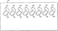
图1示出了根据本发明制造的阵列器件10。如将在下文更全面解释的,器件10包括多个在更大的电子器件中可以彼此独立使用的滤波电路。每个独立的滤波电路优选包括具有相反极性的焊料末端,例如末端12和14。焊料末端可以成型为呈众所周知的焊球阵列(BGA)排列的焊料球,或焊料可以通过许多公知技术诸如蒸镀或电镀而涂覆在独立电路的引线焊点上。Figure 1 shows an
在图2中,器件10安装在印刷电路板16上。如所示,器件10是倒装的,于是在其“顶”上的末端12和14电连接至电路板16的电路迹线(circuittrace)上。除了提供到外部线路的电连接外,焊料凸起用于将器件10维持在板子上的其物理位置上。In FIG. 2 ,
在尺寸上和/或系统成本上,制备作为小型单一封装一部分的多个电路可以获得多种优点。例如,因为对在制造工艺中拾取并放置多个分立元件的需要将被消除,所以系统成本可以降低。小的尺寸还可以保存板子的“不动产”,这通常是比小成本改善更重要的考虑因素。阵列器件到电路板的小尺寸和直接毗邻还导致非常低的ISL,通常小于1nH。Fabricating multiple circuits as part of a small single package can provide several advantages in terms of size and/or system cost. For example, system cost can be reduced because the need to pick and place multiple discrete components in the manufacturing process will be eliminated. The small size also preserves the "real estate" of the board, which is often a more important consideration than small cost improvements. The small size and direct proximity of the array devices to the board also results in very low ISL, typically less than 1nH.
现在参照图3,器件10在图示实施例中配置成具有总共八个独立RC电路18的集成阵列。如所示,每个独立电路在一对引线焊点20和22之间延伸。引线焊点上方的区域用焊料填充以产生上述的焊料末端12和14。Referring now to FIG. 3 ,
现在参照图4,在此情形中RC电路18排列成串联RC电路。换句话说,每个电路包括与相应的电容器(C1-C8)串联连接的相应的电阻器(R1-R8)。独立电路被电隔离开,使得一个电路可以单独地沿外部线路中与其它电路完全不同的线而被连接。Referring now to FIG. 4, in this case the
然而,应当意识到的是,根据本发明教导的内容,也可以实现各种其它电路配置。例如,在设置多个串联RC电路的位置上,独立电路可以在一侧上被连接到一起以形成公共接地。在这种情形中,电路在其输入端各自具有相应的末端,但在其输出端将共享一单一末端。It should be appreciated, however, that various other circuit configurations may be implemented in accordance with the teachings of the present invention. For example, where multiple series RC circuits are provided, the individual circuits may be connected together on one side to form a common ground. In this case, the circuits would each have corresponding terminals at their inputs, but would share a single terminal at their outputs.
图4A和4B说明又一种类型的电路,它可以在本发明的阵列器件中实现。具体地,图4A示出了具有连同一个电容器C1的一对电阻器R1和R1′的三端“T滤波器”。相似地,图4B示出了四端微分滤波器布置。显然应当理解的是,器件上的所有RC电路没有必要等同,但可以为了具体应用的急需情况而定制。Figures 4A and 4B illustrate yet another type of circuitry that may be implemented in the array device of the present invention. Specifically, FIG. 4A shows a three-terminal "T-filter" having a pair of resistors R1 and R1' along with a capacitor C1. Similarly, Figure 4B shows a four-terminal differential filter arrangement. It should obviously be understood that all RC circuits on a device are not necessarily identical, but can be customized to the exigencies of a particular application.
在图示实施例中,RC电路18根据薄膜加工技术构造。连续地形成许多层(这将在下面更全面地阐述)以形成所要求的电路配置。如图5中可见,各种层沉积在基板24上,该基板通常是绝缘基板,例如氧化硅、玻璃或Al2O3。在许多实施例中,基板24的厚度可以是约0.3至1.2mm。In the illustrated embodiment, the
现在将阐述每个RC电路18中的各层。导电层26定位在基板24的顶部表面上。导电层26被适当地构图以形成第一电容器极板并提供到引线焊点20的互连。所选介电材料层28设置在通过导电层26形成的电容器极板上。于是介电层与下部电容器极板并置,并与之邻近。另一导电层30的一部分在介电层26上延伸。这将提供与第一电容器极板相对的第二电容器板板,以制造电容器。The various layers in each
通常,在每个RC电路18中采用的薄膜电容器将使用高K电介质,以在要求极小极板面积的同时实现较大的电容值。例如,通常需要使用具有约100或更大的介电常数的介电材料。大于约500的介电常数通常将是优选的,而高至10,000的介电常数可以用于一些示范性实施例中。Typically, the film capacitors employed in each
例如Pb(Zr,Ti)O3(称为PZT)的某些铅基电介质可以用在本发明的优选实施例中。通常,PZT可以掺杂Nb或其它合适的掺杂剂,因而产生PNZT材料。PZT电介质的各特征在授予Lee的美国专利第5,625,529中得以说明,此处引用作为参考。所使用的另一种材料是铌镁酸铅-钛酸铅,Pb(Mg1/3Nb2/3)O3-PbTiO3。Certain lead based dielectrics such as Pb(Zr,Ti)O3 (known as PZT) may be used in preferred embodiments of the present invention. Typically, PZT can be doped with Nb or other suitable dopants, thus creating a PNZT material. Features of PZT dielectrics are described in US Patent No. 5,625,529 to Lee, incorporated herein by reference. Another material used is lead magnesium niobate-lead titanate, Pb(Mg1/3 Nb2/3 )O3 -PbTiO3 .
另外,在某些实施例中,各种非铅材料也可以用作电介质。这种材料的例子包括钛酸锶钡(Sr,Ba)TiO3和钽酸铋锶Bi2SrTa2O9。Additionally, various non-lead materials may also be used as dielectrics in certain embodiments. Examples of such materials include barium strontium titanate (Sr,Ba)TiO3 and strontium bismuth tantalate Bi2 SrTa2 O9 .
还如图5中所示,导电层30的余下部分提供了到也位于基板24上的薄膜电阻器上的电性互连。在此实施例中,电阻器通过在其上具有导电层部分34和36的电阻层32而形成。如同将在以下全面阐述的那样,部分34和36开始为电阻层32上的连续层。然后去除该连续导电层的选定区域以显露下面的电阻器材料。除掉的连续层的量将确定所得电阻器的电阻值。导电层部分36被电连接至引线焊点22,如图所示,以完成串联RC布线。As also shown in FIG. 5 , the remainder of
各层用适当的外涂层或封装38覆盖。封装38保护下部的电路免遭擦刮和腐蚀,还提供电学稳定性。如图所示,封装38被适当地构图以显露引线焊点。在示范性实施例中,合适的封装材料38可以从诸如氮化硅(Si3N4)、氧化硅(SiO2)、硅氮氧化物(SiON)和标识为SivHwCxOyN2的各种非化学配比化合物的无机材料薄膜中选取。另一种方案是,封装可以由包括聚酰亚胺、环氧树脂或苯并环丁烯(BCB)的各种有机聚合物膜以及无机和有机材料的组合层制造。The layers are covered with a suitable overcoat or encapsulation 38 . Encapsulation 38 protects the underlying circuitry from scratches and corrosion, and also provides electrical stability. As shown, package 38 is suitably patterned to reveal the lead pads. In an exemplary embodiment, suitable encapsulating material 38 may be selected frommaterials such as silicon nitride (Si3 N4 ), silicon oxide (SiO2 ),silicon oxynitride(SiON ), andN2 is selected from various non-stoichiometric compounds of inorganic material thin films. Alternatively, the encapsulation can be fabricated from various organic polymer films including polyimide, epoxy, or benzocyclobutene (BCB), as well as combined layers of inorganic and organic materials.
虽然在附图所示的示范性实施例中设置了八个RC电路,但是应当认识到,根据本发明可以提供更多或更少数量的电路。例如,根据此处教导的内容可以容易地提供少至四个或多至100个分立RC的组合物。通常,每个这种电阻器的值将在约5欧姆至约500千欧姆的范围内。电容器将通常具有在约4皮法至约100,000皮法范围内的值。Although eight RC circuits are provided in the exemplary embodiment shown in the drawings, it will be appreciated that a greater or lesser number of circuits may be provided in accordance with the invention. For example, compositions of as few as four or as many as 100 discrete RCs can readily be provided in accordance with the teachings herein. Typically, the value of each such resistor will be in the range of about 5 ohms to about 500 kiloohms. The capacitor will typically have a value in the range of about 4 picofarads to about 100,000 picofarads.
尽管事实是器件10在一单一封装中具有多个电路,但是器件10的外部尺寸通常是非常小的。例如,该器件在边缘上的长度和宽度处于约0.3mm至5.0mm的范围内并不罕见。将被意识到的是,器件10的长度和宽度通常将由电元件的数量和值,或引线数量和相应引线间的间距确定。例如,构想在本发明的许多实施例中邻近末端之间的间距可以至少是100μm。Despite the fact that
图6A至6E示出器件10的制造中采用的各步骤。首先参照图6A,对于将要制造的每个RC电路,相应的导电层26确定在基板24上。在涂覆金属前,基板24优选地被抛光和清洁以提供适于进一步加工的光滑表面。然后通过各种薄膜沉积技术中的任何一种,例如溅射或蒸镀,涂覆连同任何所需的粘接层一起的铂或其它合适的金属层。例如通过标准光刻技术构图该金属,以形成导电层26的构图。6A to 6E illustrate steps taken in the fabrication of
图6B示出相应的介电层28,它被涂覆以覆盖每个导电层26的选定部分。如上所述,介电层28可以是具有较高介电常数的铅基电介质。根据优选方法论,电介质通过溶胶-凝胶旋涂工艺涂覆。材料的粘度特性和旋转速度控制了涂覆的膜的厚度。接着按需要构图该膜并煅烧。FIG. 6B shows a corresponding
特别优选运用涂覆较厚的涂层环的溶胶-凝胶工艺,以通过较少的涂层实现给定的层厚。例如,可以采用1,3-丙二醇基PZT溶液合成物,以涂镀具有每旋转浇铸循环0.2-0.8μm厚的PZT膜。如此,可以仅需要两层涂层以达到约0.4-1.6μm的所需厚度水平。这是与许多传统溶胶-凝胶技术比较,通过每个循环它们仅可以达到约0.1μm的厚度。此处可以使用的溶胶-凝胶涂镀工艺的更详细的描述在《结合铁电体(Integrated Ferroelectrics)》1997年第18卷第263-274页Liu等人的文章“使用二元醇基化学溶液方法的铅尖晶石厚层的沉积(Thick Layer Deposition of Lead Perovskites UsingDiol-Based Chemical Solution Approch)”中给出。在与本发明具有共同受让人的专利申请第09/034,754号中也描述了这种溶胶-凝胶加工的某些特征,此处引用作为参考。Particular preference is given to using a sol-gel process for applying thicker coating rings in order to achieve a given layer thickness with fewer layers. For example, a 1,3-propanediol based PZT solution composition can be used to coat a PZT film having a thickness of 0.2-0.8 μm per spin-casting cycle. As such, only two coating layers may be required to achieve the desired thickness level of about 0.4-1.6 μm. This is in contrast to many traditional sol-gel techniques, which can only achieve a thickness of about 0.1 μm with each cycle. A more detailed description of the sol-gel coating process that can be used here is in the article "Using Diol-based Chemistry" by Liu et al., "Integrated Ferroelectrics" (Integrated Ferroelectrics), Vol. Thick Layer Deposition of Lead Perovskites Using Diol-Based Chemical Solution Approch". Certain features of this sol-gel processing are also described in common assignee application Ser. No. 09/034,754, incorporated herein by reference.
现在参照图6C,为将要制造的每个RC电路形成包括两个相邻材料的组合物的构图40。为此目的,涂覆电阻材料的第一膜,此膜可以由公知的电阻材料(例如,氮化钽、镍铬、TaAl、TaAlN、SiCr、CrSiO或金属陶瓷)中的任何一种制造。然后将适当的导电材料的第二膜覆盖在电阻材料上。公知的适当的导体中的任何一种可以用于此目的,包括金、钯、铜、铝及其相应的粘接层。然后通过光刻或其它适当的构图技术形成构图40。Referring now to FIG. 6C, a
接着,如图6D所示,从构图40的将要形成电阻器的区域除去导电材料。因为在此区域仅剩下电阻材料,所以当电阻器在复合结构的其它部分中时它将不会被短路。通过去除的导电材料的量可以非常精确地控制电阻值。Next, as shown in FIG. 6D, the conductive material is removed from the areas of
现在参照图6E,然后可以以与其它导电层相似的方式形成另外的构图导体,以完成RC电路。例如,相应的导电层30形成每个电容器的顶部极板,还提供到相应薄膜电阻器的互连。此时,还可以形成引线焊点20和22。然后如上所述封装形成在基板24上的各个层。例如通过光刻来构图封装材料,以显露引线焊点。Referring now to Figure 6E, additional patterned conductors can then be formed in a similar manner to the other conductive layers to complete the RC circuit. For example, a respective
图7示出了与上述实施例相比可以简化制造工艺的另一实施例。如上所述,在基板24的表面上形成导电层26和介电层28。然而,如所示,可以同时制造完成每个RC电路所需要的所有剩余线路。FIG. 7 shows another embodiment that can simplify the manufacturing process compared with the above-mentioned embodiment.
具体地,剩余线路由与在前述实施例中被用于仅生产电阻器的结构类似的复合电阻器/电容器结构制造。于是,引线焊点20′、引线焊点22′和导电层30′每一个均构成位于电阻材料层上的导电层。该电阻层被覆盖的导体短路,并且在此位置不明显影响电路运行。事实上,电阻层有利地取代了粘接层并充当粘接层,然而该粘接层在导电材料下方已经被使用了。在需要电阻器的位置,如上所述除去覆盖的导电层。Specifically, the remaining lines are fabricated from a composite resistor/capacitor structure similar to that used to produce only resistors in the previous embodiments. Thus, the wire pads 20', the wire pads 22' and the conductive layer 30' each constitute a conductive layer overlying the layer of resistive material. The resistive layer is shorted by the covered conductor and does not significantly affect circuit operation at this location. In fact, the resistive layer advantageously replaces and acts as the adhesive layer, which however has already been used underneath the conductive material. Where resistors are desired, remove the covering conductive layer as described above.
在层之间制造垂直电连接中,电阻层32′没有降低器件的性能。在所有实施例中,层32′的厚度远远小于接触的面积。因为接触电阻正比于由接触区域隔开的层32′的厚度,所以接触电阻将可忽略地小。The resistive layer 32' does not degrade device performance in making vertical electrical connections between the layers. In all embodiments, the thickness of layer 32' is much smaller than the area of contact. Since the contact resistance is proportional to the thickness of the layer 32' separated by the contact areas, the contact resistance will be negligibly small.
在图示的实施例中,在远离第二电容器极板的位置形成电阻器(通过导电层/电阻层组合物的部分30′形成)。然而,也可以构想的是,电阻器可以通过去除第二电容器极板处的导电层而形成。在这些实施例中,此位置上的电阻层将既用作电阻器又用作第二电容器极板。据信,通过这种布置形成的分布式RC的特性在本发明的许多潜在应用中可能是有利的。In the illustrated embodiment, the resistor is formed at a location remote from the second capacitor plate (formed by portion 30' of the conductive layer/resistive layer composition). However, it is also contemplated that the resistor may be formed by removing the conductive layer at the second capacitor plate. In these embodiments, the resistive layer at this location will function as both a resistor and a second capacitor plate. It is believed that the nature of the distributed RC formed by this arrangement may be advantageous in many potential applications of the present invention.
图8示出在许多方面与图5所示的实施例相似的备选实施例。为了简便起见,与图5的实施例中的那些相似或类似的组元用加上100的附图标记表示。然而,在此种情况中,设置适应层以吸收器件和将要安装它的电路板之间的应力。FIG. 8 shows an alternative embodiment similar in many respects to the embodiment shown in FIG. 5 . Components that are similar or analogous to those in the embodiment of FIG. 5 are denoted by reference numerals increased by 100 for simplicity. In this case, however, a compliant layer is provided to absorb the stress between the device and the circuit board on which it will be mounted.
具体地,封装层138用作适应层,以避免因器件和电路板的热膨胀上的不同所导致的引线焊点上的横向力引起的应变。在封装层138的顶部上制备金属化的附加层,以形成附加引线焊点120′和122′。于是附加金属层将引线焊点从先前位置重新分布到封装层138上的位置上。然后在结构的余下部分上设置另一封装层138′。在封装层138′上确定开口,以便将显露引线焊点120′和122′。In particular,
图9示出又一个实施例,它也与图5的实施例相似,其中,相似或类似的组元将用加上200的附图标记表示。在此情况中,绝缘基板224由硅的第一层242制造,该第一层在其如244处表示的表面上被氧化而制备绝缘层。形成引线焊点220的被电连接到第一电容器极板226上的层通过氧化层上的通孔246接地到硅层242上。这种布图将有利地提供一些寄生电容。FIG. 9 shows yet another embodiment, which is also similar to the embodiment of FIG. 5 , wherein similar or analogous components will be indicated with reference numerals increased by 200. In this case, the insulating substrate 224 is manufactured from a first layer 242 of silicon, which is oxidized on its surface as indicated at 244 to produce an insulating layer. The layer forming the lead pad 220 that is electrically connected to the first capacitor plate 226 is grounded to the silicon layer 242 through a via 246 in the oxide layer. This layout will advantageously provide some parasitic capacitance.
如图9所示的接地布图的益处可以参照图10极其容易地解释。曲线248示出了诸如图4A中那样的“T滤波器”的频率响应的理论理想值。曲线250和252分别示出了被制造为不具有和具有基板接地的理想电路的性能。The benefits of the ground pattern shown in FIG. 9 can be explained most easily with reference to FIG. 10 . Curve 248 shows the theoretical ideal value of the frequency response of a "T filter" such as that in FIG. 4A. Curves 250 and 252 show the performance of an idealized circuit fabricated without and with substrate grounding, respectively.
在此理想情况中,如曲线248所示,随频率增加,信号愈加阻塞至一极限。在没有接地的真实电路的情形中,如曲线250所示,一旦过了因电感导致的最小值,传输增加。于是,参照曲线252易看出接地的重要性。当附加上有益的寄生电容时,信号被维持在理想情况的容限内。In this ideal case, as shown by curve 248, as the frequency increases, the signal becomes increasingly blocked up to a limit. In the case of a real circuit without ground, as shown by curve 250, once the minimum due to inductance is passed, the transmission increases. Thus, the importance of grounding is readily seen with reference to curve 252 . When adding beneficial parasitic capacitance, the signal is maintained within ideal-case tolerances.
可以看出,本发明提供了希望在非常小尺寸的封装中具有电路组元的高度集中的集成阵列。本领域的技术人员将意识到,在不背离本发明的情况下可以作出各种变化和修改。It can be seen that the present invention provides a highly concentrated integrated array of desirable circuit components in a package of very small size. Those skilled in the art will appreciate that various changes and modifications can be made without departing from the invention.
例如,附图中所示的每个实施例使用电容器极板被设置成一个在另一个顶部的电容器布图。然而,应当意识到的是,本发明教导的内容中包括各种其它类型的电容器结构。在这一点上,在一些应用中,可能需要把电容器形成为“间隙盖(gap cap)”,其中共面的电容器电极定位在电介质表面上,并被一预定的间隙隔开。For example, each of the embodiments shown in the figures uses a capacitor layout in which capacitor plates are arranged one on top of the other. It should be appreciated, however, that various other types of capacitor structures are included within the teachings of the present invention. In this regard, in some applications it may be desirable to form the capacitor as a "gap cap" in which coplanar capacitor electrodes are positioned on the dielectric surface and separated by a predetermined gap.
另外,上述实施例说明了绝缘的或在形成电路组元前被制作成绝缘的基板。在一些实施例中,例如被配置成具有公共接地的那些实施例,需要使用导电基板。在使用导电基板的情况中,通常需要用离散的绝缘体隔离一些电路组元,例如电阻器。Additionally, the above-described embodiments illustrate substrates that are insulated or made to insulate prior to forming circuit components. In some embodiments, such as those configured with a common ground, the use of a conductive substrate is required. Where conductive substrates are used, it is often necessary to isolate some circuit components, such as resistors, with discrete insulators.
本领域的技术人员也将意识到,各实施例的各方面既可以在整体上也可以在部分上互换。另外,本领域的普通技术人员将意识到,前述仅仅是示例,并不意味是对在其所附权利要求书中进一步描述的本发明的限制。Those skilled in the art will also appreciate that aspects of the various embodiments may be interchanged in whole or in part. Additionally, those of ordinary skill in the art will appreciate that the foregoing are examples only, and are not meant to be limiting of the invention, which is further described in the appended claims.
Claims (27)
Applications Claiming Priority (2)
| Application Number | Priority Date | Filing Date | Title |
|---|---|---|---|
| US09/293,817US6285542B1 (en) | 1999-04-16 | 1999-04-16 | Ultra-small resistor-capacitor thin film network for inverted mounting to a surface |
| US09/293,817 | 1999-04-16 |
Publications (1)
| Publication Number | Publication Date |
|---|---|
| CN1350690Atrue CN1350690A (en) | 2002-05-22 |
Family
ID=23130711
Family Applications (1)
| Application Number | Title | Priority Date | Filing Date |
|---|---|---|---|
| CN00807349.XAPendingCN1350690A (en) | 1999-04-16 | 2000-04-10 | Ultraminiature resistor-capacitor thin-film networks for flip-chip mounting on surfaces |
Country Status (7)
| Country | Link |
|---|---|
| US (1) | US6285542B1 (en) |
| JP (1) | JP2002542619A (en) |
| CN (1) | CN1350690A (en) |
| AU (1) | AU4226500A (en) |
| DE (1) | DE10084476T1 (en) |
| GB (1) | GB2367190B (en) |
| WO (1) | WO2000063928A1 (en) |
Cited By (2)
| Publication number | Priority date | Publication date | Assignee | Title |
|---|---|---|---|---|
| CN106067378A (en)* | 2015-04-20 | 2016-11-02 | 阿维科斯公司 | Wire bonding transmission line RC circuit |
| CN106067842A (en)* | 2015-04-20 | 2016-11-02 | 阿维科斯公司 | Parallel RC Circuit Equalizer |
Families Citing this family (75)
| Publication number | Priority date | Publication date | Assignee | Title |
|---|---|---|---|---|
| US6606011B2 (en) | 1998-04-07 | 2003-08-12 | X2Y Attenuators, Llc | Energy conditioning circuit assembly |
| US7336467B2 (en) | 2000-10-17 | 2008-02-26 | X2Y Attenuators, Llc | Energy pathway arrangement |
| US20030161086A1 (en) | 2000-07-18 | 2003-08-28 | X2Y Attenuators, Llc | Paired multi-layered dielectric independent passive component architecture resulting in differential and common mode filtering with surge protection in one integrated package |
| US7321485B2 (en) | 1997-04-08 | 2008-01-22 | X2Y Attenuators, Llc | Arrangement for energy conditioning |
| US7042703B2 (en) | 2000-03-22 | 2006-05-09 | X2Y Attenuators, Llc | Energy conditioning structure |
| US7106570B2 (en) | 1997-04-08 | 2006-09-12 | Xzy Altenuators, Llc | Pathway arrangement |
| US9054094B2 (en) | 1997-04-08 | 2015-06-09 | X2Y Attenuators, Llc | Energy conditioning circuit arrangement for integrated circuit |
| US6894884B2 (en) | 1997-04-08 | 2005-05-17 | Xzy Attenuators, Llc | Offset pathway arrangements for energy conditioning |
| US20020079116A1 (en) | 2000-10-17 | 2002-06-27 | X2Y Attenuators, Llc | Amalgam of shielding and shielded energy pathways and other elements for single or multiple circuitries with common reference node |
| US6018448A (en)* | 1997-04-08 | 2000-01-25 | X2Y Attenuators, L.L.C. | Paired multi-layered dielectric independent passive component architecture resulting in differential and common mode filtering with surge protection in one integrated package |
| US6603646B2 (en) | 1997-04-08 | 2003-08-05 | X2Y Attenuators, Llc | Multi-functional energy conditioner |
| US6650525B2 (en) | 1997-04-08 | 2003-11-18 | X2Y Attenuators, Llc | Component carrier |
| US7301748B2 (en) | 1997-04-08 | 2007-11-27 | Anthony Anthony A | Universal energy conditioning interposer with circuit architecture |
| US7110227B2 (en) | 1997-04-08 | 2006-09-19 | X2Y Attenuators, Llc | Universial energy conditioning interposer with circuit architecture |
| US7336468B2 (en) | 1997-04-08 | 2008-02-26 | X2Y Attenuators, Llc | Arrangement for energy conditioning |
| US7274549B2 (en) | 2000-12-15 | 2007-09-25 | X2Y Attenuators, Llc | Energy pathway arrangements for energy conditioning |
| US7110235B2 (en) | 1997-04-08 | 2006-09-19 | Xzy Altenuators, Llc | Arrangement for energy conditioning |
| US7427816B2 (en) | 1998-04-07 | 2008-09-23 | X2Y Attenuators, Llc | Component carrier |
| EP1070389B1 (en) | 1998-04-07 | 2007-12-05 | X2Y Attenuators, L.L.C. | Component carrier |
| US6262877B1 (en)* | 1999-11-23 | 2001-07-17 | Intel Corporation | Low inductance high capacitance capacitor and method of making same |
| US7113383B2 (en) | 2000-04-28 | 2006-09-26 | X2Y Attenuators, Llc | Predetermined symmetrically balanced amalgam with complementary paired portions comprising shielding electrodes and shielded electrodes and other predetermined element portions for symmetrically balanced and complementary energy portion conditioning |
| IL154413A0 (en) | 2000-08-15 | 2003-09-17 | X2Y Attenuators Llc | An electrode arrangement for circuit energy conditioning |
| US7193831B2 (en) | 2000-10-17 | 2007-03-20 | X2Y Attenuators, Llc | Energy pathway arrangement |
| US6489850B2 (en)* | 2001-03-16 | 2002-12-03 | International Business Machines Corporation | Crosstalk suppression in differential AC coupled multichannel IC amplifiers |
| TW563142B (en)* | 2001-07-12 | 2003-11-21 | Hitachi Ltd | Thin film capacitor, and electronic circuit component |
| US6709882B2 (en)* | 2001-08-27 | 2004-03-23 | Lightwave Microsystems Corporation | Planar lightwave circuit active device metallization process |
| US6657522B2 (en)* | 2002-02-01 | 2003-12-02 | M/A-Com | Wide bandwidth bias tee |
| US7002435B2 (en)* | 2002-09-27 | 2006-02-21 | Kyocera Corporation | Variable capacitance circuit, variable capacitance thin film capacitor and radio frequency device |
| US6897761B2 (en)* | 2002-12-04 | 2005-05-24 | Cts Corporation | Ball grid array resistor network |
| US6819569B1 (en)* | 2002-12-06 | 2004-11-16 | Thin Film Technology Corp. | Impedance equalization module |
| US7180718B2 (en) | 2003-01-31 | 2007-02-20 | X2Y Attenuators, Llc | Shielded energy conditioner |
| US6950300B2 (en)* | 2003-05-06 | 2005-09-27 | Marvell World Trade Ltd. | Ultra low inductance multi layer ceramic capacitor |
| EP1629582A2 (en) | 2003-05-29 | 2006-03-01 | X2Y Attenuators, L.L.C. | Connector related structures including an energy conditioner |
| EP1649572A4 (en) | 2003-07-21 | 2012-06-27 | X2Y Attenuators Llc | Filter assembly |
| WO2005025029A1 (en)* | 2003-09-03 | 2005-03-17 | Matsushita Electric Industrial Co., Ltd. | Capacitor device and wiring pattern |
| CN1890854A (en) | 2003-12-22 | 2007-01-03 | X2Y艾泰钮埃特有限责任公司 | Internally shielded energy conditioner |
| EP1751499B1 (en)* | 2004-06-03 | 2012-04-04 | Making Virtual Solid, L.L.C. | En-route navigation display method and apparatus using head-up display |
| US7092232B2 (en)* | 2004-06-28 | 2006-08-15 | Kyocera Corporation | Variable capacitance capacitor, circuit module, and communications apparatus |
| US7342804B2 (en)* | 2004-08-09 | 2008-03-11 | Cts Corporation | Ball grid array resistor capacitor network |
| US7430128B2 (en)* | 2004-10-18 | 2008-09-30 | E.I. Du Pont De Nemours And Company | Capacitive/resistive devices, organic dielectric laminates and printed wiring boards incorporating such devices, and methods of making thereof |
| JP2006135131A (en)* | 2004-11-08 | 2006-05-25 | Toppan Printing Co Ltd | Resistor capacitor composite element |
| JP4566012B2 (en)* | 2005-01-13 | 2010-10-20 | 京セラ株式会社 | Variable capacitor, circuit module and communication device |
| WO2006093831A2 (en) | 2005-03-01 | 2006-09-08 | X2Y Attenuators, Llc | Energy conditioner with tied through electrodes |
| JP2008535207A (en) | 2005-03-01 | 2008-08-28 | エックストゥーワイ アテニュエイターズ,エルエルシー | Regulator with coplanar conductor |
| WO2006099297A2 (en) | 2005-03-14 | 2006-09-21 | X2Y Attenuators, Llc | Conditioner with coplanar conductors |
| US20060286696A1 (en)* | 2005-06-21 | 2006-12-21 | Peiffer Joel S | Passive electrical article |
| US8257463B2 (en)* | 2006-01-23 | 2012-09-04 | Avx Corporation | Capacitor anode formed from flake powder |
| WO2007103965A1 (en) | 2006-03-07 | 2007-09-13 | X2Y Attenuators, Llc | Energy conditioner structures |
| US7375948B2 (en)* | 2006-06-12 | 2008-05-20 | Teledyne Licensing, Llc | Variable charge packet integrated circuit capacitor |
| US7280343B1 (en) | 2006-10-31 | 2007-10-09 | Avx Corporation | Low profile electrolytic capacitor assembly |
| US20090223700A1 (en)* | 2008-03-05 | 2009-09-10 | Honeywell International Inc. | Thin flexible circuits |
| US20100085685A1 (en)* | 2008-10-06 | 2010-04-08 | Avx Corporation | Capacitor Anode Formed From a Powder Containing Coarse Agglomerates and Fine Agglomerates |
| US9450556B2 (en) | 2009-10-16 | 2016-09-20 | Avx Corporation | Thin film surface mount components |
| US8382524B2 (en)* | 2010-05-21 | 2013-02-26 | Amphenol Corporation | Electrical connector having thick film layers |
| US20110287663A1 (en) | 2010-05-21 | 2011-11-24 | Gailus Mark W | Electrical connector incorporating circuit elements |
| US9240644B2 (en) | 2012-08-22 | 2016-01-19 | Amphenol Corporation | High-frequency electrical connector |
| US9093974B2 (en) | 2012-09-05 | 2015-07-28 | Avx Corporation | Electromagnetic interference filter for implanted electronics |
| US9472904B2 (en)* | 2014-08-18 | 2016-10-18 | Amphenol Corporation | Discrete packaging adapter for connector |
| US9685736B2 (en) | 2014-11-12 | 2017-06-20 | Amphenol Corporation | Very high speed, high density electrical interconnection system with impedance control in mating region |
| TWI746561B (en) | 2016-05-31 | 2021-11-21 | 美商安芬諾股份有限公司 | High performance cable termination |
| CN110088985B (en) | 2016-10-19 | 2022-07-05 | 安费诺有限公司 | Flexible shield for ultra-high speed high density electrical interconnects |
| TWI788394B (en) | 2017-08-03 | 2023-01-01 | 美商安芬諾股份有限公司 | Cable assembly and method of manufacturing the same |
| US10665973B2 (en) | 2018-03-22 | 2020-05-26 | Amphenol Corporation | High density electrical connector |
| WO2019195319A1 (en) | 2018-04-02 | 2019-10-10 | Ardent Concepts, Inc. | Controlled-impedance compliant cable termination |
| US10931062B2 (en) | 2018-11-21 | 2021-02-23 | Amphenol Corporation | High-frequency electrical connector |
| WO2020154507A1 (en) | 2019-01-25 | 2020-07-30 | Fci Usa Llc | I/o connector configured for cable connection to a midboard |
| US11101611B2 (en) | 2019-01-25 | 2021-08-24 | Fci Usa Llc | I/O connector configured for cabled connection to the midboard |
| WO2020172395A1 (en) | 2019-02-22 | 2020-08-27 | Amphenol Corporation | High performance cable connector assembly |
| CN114788097A (en) | 2019-09-19 | 2022-07-22 | 安费诺有限公司 | High speed electronic system with midplane cable connector |
| TWI887339B (en) | 2020-01-27 | 2025-06-21 | 美商Fci美國有限責任公司 | High speed, high density direct mate orthogonal connector |
| WO2021154702A1 (en) | 2020-01-27 | 2021-08-05 | Fci Usa Llc | High speed connector |
| CN113258325A (en) | 2020-01-28 | 2021-08-13 | 富加宜(美国)有限责任公司 | High-frequency middle plate connector |
| US11792983B2 (en) | 2020-08-28 | 2023-10-17 | Micron Technology, Inc. | Integrated circuitry comprising a memory array comprising strings of memory cells and methods used in forming a memory array comprising strings of memory cells |
| US11552090B2 (en) | 2020-08-28 | 2023-01-10 | Micron Technology, Inc. | Integrated circuitry comprising a memory array comprising strings of memory cells and methods used in forming a memory array comprising strings of memory cells |
| USD1002553S1 (en) | 2021-11-03 | 2023-10-24 | Amphenol Corporation | Gasket for connector |
Family Cites Families (31)
| Publication number | Priority date | Publication date | Assignee | Title |
|---|---|---|---|---|
| US3273033A (en) | 1963-08-29 | 1966-09-13 | Litton Systems Inc | Multidielectric thin film capacitors |
| US3268744A (en) | 1964-04-16 | 1966-08-23 | Ibm | High capacitance microelectronic decoupling device with low shunt resistance at high frequencies |
| US3778689A (en) | 1972-05-22 | 1973-12-11 | Hewlett Packard Co | Thin film capacitors and method for manufacture |
| US4251326A (en) | 1978-12-28 | 1981-02-17 | Western Electric Company, Inc. | Fabricating an RC network utilizing alpha tantalum |
| US4410867A (en) | 1978-12-28 | 1983-10-18 | Western Electric Company, Inc. | Alpha tantalum thin film circuit device |
| US4971924A (en) | 1985-05-01 | 1990-11-20 | Texas Instruments Incorporated | Metal plate capacitor and method for making the same |
| US4821085A (en) | 1985-05-01 | 1989-04-11 | Texas Instruments Incorporated | VLSI local interconnect structure |
| US4801469A (en) | 1986-08-07 | 1989-01-31 | The United States Of America As Represented By The Department Of Energy | Process for obtaining multiple sheet resistances for thin film hybrid microcircuit resistors |
| US5108941A (en) | 1986-12-05 | 1992-04-28 | Texas Instrument Incorporated | Method of making metal-to-polysilicon capacitor |
| US4788524A (en) | 1987-08-27 | 1988-11-29 | Gte Communication Systems Corporation | Thick film material system |
| US4933208A (en) | 1987-11-16 | 1990-06-12 | Motorola, Inc. | Multilayer thermoplastic substrate and method of manufacture |
| US5079670A (en) | 1988-05-03 | 1992-01-07 | Texas Instruments Incorporated | Metal plate capacitor and method for making the same |
| US5093774A (en) | 1991-03-22 | 1992-03-03 | Thomas & Betts Corporation | Two-terminal series-connected network |
| US5420745A (en) | 1991-09-30 | 1995-05-30 | Matsushita Electric Industrial Co., Ltd. | Surface-mount type ceramic capacitor |
| JPH0590502A (en)* | 1991-09-30 | 1993-04-09 | Nec Corp | Semiconductor device |
| US5206788A (en) | 1991-12-12 | 1993-04-27 | Ramtron Corporation | Series ferroelectric capacitor structure for monolithic integrated circuits and method |
| US5288660A (en) | 1993-02-01 | 1994-02-22 | Avantek, Inc. | Method for forming self-aligned t-shaped transistor electrode |
| US5370766A (en) | 1993-08-16 | 1994-12-06 | California Micro Devices | Methods for fabrication of thin film inductors, inductor networks and integration with other passive and active devices |
| JPH0766325A (en) | 1993-08-26 | 1995-03-10 | Rohm Co Ltd | Structure of synthetic resin package type electronic component |
| JPH07249542A (en)* | 1994-03-14 | 1995-09-26 | Nippon Carbide Ind Co Inc | Network array |
| US5457598A (en) | 1994-04-08 | 1995-10-10 | Radford; Kenneth C. | High capacitance thin film capacitor |
| JPH07283077A (en) | 1994-04-11 | 1995-10-27 | Ngk Spark Plug Co Ltd | Thin film capacitor |
| JPH08130161A (en)* | 1994-10-31 | 1996-05-21 | Kyocera Corp | Chip RC network |
| TW367621B (en) | 1995-02-27 | 1999-08-21 | Nxp Bv | Electronic component comprising a thin-film structure with passive elements |
| US5625529A (en) | 1995-03-28 | 1997-04-29 | Samsung Electronics Co., Ltd. | PZT thin films for ferroelectric capacitor and method for preparing the same |
| US5822175A (en)* | 1995-04-13 | 1998-10-13 | Matsushita Electronics Corporation | Encapsulated capacitor structure having a dielectric interlayer |
| JP3323091B2 (en)* | 1996-01-18 | 2002-09-09 | 東芝マイクロエレクトロニクス株式会社 | Semiconductor integrated circuit device and method of manufacturing the same |
| JP3512609B2 (en)* | 1997-09-29 | 2004-03-31 | 京セラ株式会社 | Thin film capacitors and capacitors |
| US5880925A (en) | 1997-06-27 | 1999-03-09 | Avx Corporation | Surface mount multilayer capacitor |
| US5889445A (en)* | 1997-07-22 | 1999-03-30 | Avx Corporation | Multilayer ceramic RC device |
| JP2001015381A (en)* | 1999-06-28 | 2001-01-19 | Hokuriku Electric Ind Co Ltd | Surface-mounting type composite electronic component and manufacture thereof |
- 1999
- 1999-04-16USUS09/293,817patent/US6285542B1/ennot_activeExpired - Fee Related
- 2000
- 2000-04-10CNCN00807349.XApatent/CN1350690A/enactivePending
- 2000-04-10GBGB0124694Apatent/GB2367190B/ennot_activeExpired - Fee Related
- 2000-04-10WOPCT/US2000/009580patent/WO2000063928A1/enactiveApplication Filing
- 2000-04-10DEDE10084476Tpatent/DE10084476T1/ennot_activeWithdrawn
- 2000-04-10AUAU42265/00Apatent/AU4226500A/ennot_activeAbandoned
- 2000-04-10JPJP2000612968Apatent/JP2002542619A/ennot_activeCeased
Cited By (4)
| Publication number | Priority date | Publication date | Assignee | Title |
|---|---|---|---|---|
| CN106067378A (en)* | 2015-04-20 | 2016-11-02 | 阿维科斯公司 | Wire bonding transmission line RC circuit |
| CN106067842A (en)* | 2015-04-20 | 2016-11-02 | 阿维科斯公司 | Parallel RC Circuit Equalizer |
| CN106067378B (en)* | 2015-04-20 | 2020-06-23 | 阿维科斯公司 | Wire-bonding transmission line RC circuit |
| CN106067842B (en)* | 2015-04-20 | 2020-09-11 | 阿维科斯公司 | RC circuit equalizer and method for increasing its resonant frequency and operating frequency range |
Also Published As
| Publication number | Publication date |
|---|---|
| GB0124694D0 (en) | 2001-12-05 |
| GB2367190B (en) | 2003-08-27 |
| JP2002542619A (en) | 2002-12-10 |
| DE10084476T1 (en) | 2002-03-14 |
| US6285542B1 (en) | 2001-09-04 |
| AU4226500A (en) | 2000-11-02 |
| GB2367190A (en) | 2002-03-27 |
| WO2000063928A1 (en) | 2000-10-26 |
Similar Documents
| Publication | Publication Date | Title |
|---|---|---|
| CN1350690A (en) | Ultraminiature resistor-capacitor thin-film networks for flip-chip mounting on surfaces | |
| US6832420B2 (en) | Method of manufacturing a thin film capacitor array | |
| CN1324667C (en) | Structure and Formation Method of Diffused Wafer Type Package | |
| US6624501B2 (en) | Capacitor and semiconductor device | |
| US7405921B2 (en) | Layer capacitor element and production process as well as electronic device | |
| US7439199B2 (en) | Capacitive element, method of manufacture of the same, and semiconductor device | |
| CN1783709A (en) | Electronic device and method of manufacturing the same | |
| CN1476618A (en) | Multi-connected capacitor | |
| JPH0745468A (en) | Ceramic capacitor and semiconductor device fixed therewith | |
| US7026680B2 (en) | Thin film capacitive element, method for producing same and electronic device | |
| CN1084050C (en) | Electronic components containing thin film structures with passive components | |
| JP4628520B2 (en) | Manufacturing method of electronic device mounting substrate | |
| JP2001358248A (en) | Circuit board with built-in capacitor and method of manufacturing the same | |
| JP3967964B2 (en) | Thin film electronic components | |
| JPH08241830A (en) | Thin film capacitors | |
| JP4009078B2 (en) | Thin film electronic components | |
| JP2006005309A (en) | Capacitor device | |
| JP3246166B2 (en) | Thin film capacitors | |
| JP3645808B2 (en) | Thin-film electronic component, its manufacturing method and substrate | |
| JP2000306767A (en) | Thin-film capacitor, manufacture thereof, and multilayer laminate mounting board | |
| JP2001345232A (en) | Thin film electronic components and substrates | |
| JP2000252151A (en) | Capacitors | |
| JPH07249542A (en) | Network array | |
| JP2003347156A (en) | Thin film electronic component | |
| JPH07249540A (en) | Capacitor array |
Legal Events
| Date | Code | Title | Description |
|---|---|---|---|
| C06 | Publication | ||
| PB01 | Publication | ||
| C10 | Entry into substantive examination | ||
| SE01 | Entry into force of request for substantive examination | ||
| C02 | Deemed withdrawal of patent application after publication (patent law 2001) | ||
| WD01 | Invention patent application deemed withdrawn after publication |