CN1340851A - Electronic device and its manufacture method - Google Patents
Electronic device and its manufacture methodDownload PDFInfo
- Publication number
- CN1340851A CN1340851ACN01125227ACN01125227ACN1340851ACN 1340851 ACN1340851 ACN 1340851ACN 01125227 ACN01125227 ACN 01125227ACN 01125227 ACN01125227 ACN 01125227ACN 1340851 ACN1340851 ACN 1340851A
- Authority
- CN
- China
- Prior art keywords
- electronic component
- district
- wiring plate
- type surface
- solder paste
- Prior art date
- Legal status (The legal status is an assumption and is not a legal conclusion. Google has not performed a legal analysis and makes no representation as to the accuracy of the status listed.)
- Granted
Links
Images


Classifications
- H—ELECTRICITY
- H05—ELECTRIC TECHNIQUES NOT OTHERWISE PROVIDED FOR
- H05K—PRINTED CIRCUITS; CASINGS OR CONSTRUCTIONAL DETAILS OF ELECTRIC APPARATUS; MANUFACTURE OF ASSEMBLAGES OF ELECTRICAL COMPONENTS
- H05K3/00—Apparatus or processes for manufacturing printed circuits
- H05K3/30—Assembling printed circuits with electric components, e.g. with resistor
- H05K3/32—Assembling printed circuits with electric components, e.g. with resistor electrically connecting electric components or wires to printed circuits
- H05K3/34—Assembling printed circuits with electric components, e.g. with resistor electrically connecting electric components or wires to printed circuits by soldering
- H05K3/341—Surface mounted components
- H—ELECTRICITY
- H01—ELECTRIC ELEMENTS
- H01L—SEMICONDUCTOR DEVICES NOT COVERED BY CLASS H10
- H01L21/00—Processes or apparatus adapted for the manufacture or treatment of semiconductor or solid state devices or of parts thereof
- H01L21/02—Manufacture or treatment of semiconductor devices or of parts thereof
- H01L21/04—Manufacture or treatment of semiconductor devices or of parts thereof the devices having potential barriers, e.g. a PN junction, depletion layer or carrier concentration layer
- H01L21/50—Assembly of semiconductor devices using processes or apparatus not provided for in a single one of the groups H01L21/18 - H01L21/326 or H10D48/04 - H10D48/07 e.g. sealing of a cap to a base of a container
- H01L21/60—Attaching or detaching leads or other conductive members, to be used for carrying current to or from the device in operation
- H—ELECTRICITY
- H01—ELECTRIC ELEMENTS
- H01L—SEMICONDUCTOR DEVICES NOT COVERED BY CLASS H10
- H01L24/00—Arrangements for connecting or disconnecting semiconductor or solid-state bodies; Methods or apparatus related thereto
- H01L24/01—Means for bonding being attached to, or being formed on, the surface to be connected, e.g. chip-to-package, die-attach, "first-level" interconnects; Manufacturing methods related thereto
- H01L24/26—Layer connectors, e.g. plate connectors, solder or adhesive layers; Manufacturing methods related thereto
- H01L24/27—Manufacturing methods
- H—ELECTRICITY
- H01—ELECTRIC ELEMENTS
- H01L—SEMICONDUCTOR DEVICES NOT COVERED BY CLASS H10
- H01L2224/00—Indexing scheme for arrangements for connecting or disconnecting semiconductor or solid-state bodies and methods related thereto as covered by H01L24/00
- H01L2224/01—Means for bonding being attached to, or being formed on, the surface to be connected, e.g. chip-to-package, die-attach, "first-level" interconnects; Manufacturing methods related thereto
- H01L2224/26—Layer connectors, e.g. plate connectors, solder or adhesive layers; Manufacturing methods related thereto
- H01L2224/27—Manufacturing methods
- H01L2224/27001—Involving a temporary auxiliary member not forming part of the manufacturing apparatus, e.g. removable or sacrificial coating, film or substrate
- H—ELECTRICITY
- H01—ELECTRIC ELEMENTS
- H01L—SEMICONDUCTOR DEVICES NOT COVERED BY CLASS H10
- H01L2224/00—Indexing scheme for arrangements for connecting or disconnecting semiconductor or solid-state bodies and methods related thereto as covered by H01L24/00
- H01L2224/01—Means for bonding being attached to, or being formed on, the surface to be connected, e.g. chip-to-package, die-attach, "first-level" interconnects; Manufacturing methods related thereto
- H01L2224/42—Wire connectors; Manufacturing methods related thereto
- H01L2224/44—Structure, shape, material or disposition of the wire connectors prior to the connecting process
- H01L2224/45—Structure, shape, material or disposition of the wire connectors prior to the connecting process of an individual wire connector
- H01L2224/45001—Core members of the connector
- H01L2224/45099—Material
- H01L2224/451—Material with a principal constituent of the material being a metal or a metalloid, e.g. boron (B), silicon (Si), germanium (Ge), arsenic (As), antimony (Sb), tellurium (Te) and polonium (Po), and alloys thereof
- H01L2224/45138—Material with a principal constituent of the material being a metal or a metalloid, e.g. boron (B), silicon (Si), germanium (Ge), arsenic (As), antimony (Sb), tellurium (Te) and polonium (Po), and alloys thereof the principal constituent melting at a temperature of greater than or equal to 950°C and less than 1550°C
- H01L2224/45144—Gold (Au) as principal constituent
- H—ELECTRICITY
- H01—ELECTRIC ELEMENTS
- H01L—SEMICONDUCTOR DEVICES NOT COVERED BY CLASS H10
- H01L2224/00—Indexing scheme for arrangements for connecting or disconnecting semiconductor or solid-state bodies and methods related thereto as covered by H01L24/00
- H01L2224/73—Means for bonding being of different types provided for in two or more of groups H01L2224/10, H01L2224/18, H01L2224/26, H01L2224/34, H01L2224/42, H01L2224/50, H01L2224/63, H01L2224/71
- H01L2224/732—Location after the connecting process
- H01L2224/73201—Location after the connecting process on the same surface
- H01L2224/73203—Bump and layer connectors
- H01L2224/73204—Bump and layer connectors the bump connector being embedded into the layer connector
- H—ELECTRICITY
- H01—ELECTRIC ELEMENTS
- H01L—SEMICONDUCTOR DEVICES NOT COVERED BY CLASS H10
- H01L2224/00—Indexing scheme for arrangements for connecting or disconnecting semiconductor or solid-state bodies and methods related thereto as covered by H01L24/00
- H01L2224/80—Methods for connecting semiconductor or other solid state bodies using means for bonding being attached to, or being formed on, the surface to be connected
- H01L2224/83—Methods for connecting semiconductor or other solid state bodies using means for bonding being attached to, or being formed on, the surface to be connected using a layer connector
- H01L2224/8319—Arrangement of the layer connectors prior to mounting
- H01L2224/83192—Arrangement of the layer connectors prior to mounting wherein the layer connectors are disposed only on another item or body to be connected to the semiconductor or solid-state body
- H—ELECTRICITY
- H01—ELECTRIC ELEMENTS
- H01L—SEMICONDUCTOR DEVICES NOT COVERED BY CLASS H10
- H01L2924/00—Indexing scheme for arrangements or methods for connecting or disconnecting semiconductor or solid-state bodies as covered by H01L24/00
- H01L2924/10—Details of semiconductor or other solid state devices to be connected
- H01L2924/11—Device type
- H01L2924/14—Integrated circuits
- H—ELECTRICITY
- H01—ELECTRIC ELEMENTS
- H01L—SEMICONDUCTOR DEVICES NOT COVERED BY CLASS H10
- H01L2924/00—Indexing scheme for arrangements or methods for connecting or disconnecting semiconductor or solid-state bodies as covered by H01L24/00
- H01L2924/19—Details of hybrid assemblies other than the semiconductor or other solid state devices to be connected
- H01L2924/191—Disposition
- H01L2924/19101—Disposition of discrete passive components
- H01L2924/19105—Disposition of discrete passive components in a side-by-side arrangement on a common die mounting substrate
- H—ELECTRICITY
- H05—ELECTRIC TECHNIQUES NOT OTHERWISE PROVIDED FOR
- H05K—PRINTED CIRCUITS; CASINGS OR CONSTRUCTIONAL DETAILS OF ELECTRIC APPARATUS; MANUFACTURE OF ASSEMBLAGES OF ELECTRICAL COMPONENTS
- H05K2201/00—Indexing scheme relating to printed circuits covered by H05K1/00
- H05K2201/10—Details of components or other objects attached to or integrated in a printed circuit board
- H05K2201/10613—Details of electrical connections of non-printed components, e.g. special leads
- H05K2201/10621—Components characterised by their electrical contacts
- H05K2201/10636—Leadless chip, e.g. chip capacitor or resistor
- H—ELECTRICITY
- H05—ELECTRIC TECHNIQUES NOT OTHERWISE PROVIDED FOR
- H05K—PRINTED CIRCUITS; CASINGS OR CONSTRUCTIONAL DETAILS OF ELECTRIC APPARATUS; MANUFACTURE OF ASSEMBLAGES OF ELECTRICAL COMPONENTS
- H05K2201/00—Indexing scheme relating to printed circuits covered by H05K1/00
- H05K2201/10—Details of components or other objects attached to or integrated in a printed circuit board
- H05K2201/10613—Details of electrical connections of non-printed components, e.g. special leads
- H05K2201/10621—Components characterised by their electrical contacts
- H05K2201/10674—Flip chip
- H—ELECTRICITY
- H05—ELECTRIC TECHNIQUES NOT OTHERWISE PROVIDED FOR
- H05K—PRINTED CIRCUITS; CASINGS OR CONSTRUCTIONAL DETAILS OF ELECTRIC APPARATUS; MANUFACTURE OF ASSEMBLAGES OF ELECTRICAL COMPONENTS
- H05K2203/00—Indexing scheme relating to apparatus or processes for manufacturing printed circuits covered by H05K3/00
- H05K2203/02—Details related to mechanical or acoustic processing, e.g. drilling, punching, cutting, using ultrasound
- H05K2203/0278—Flat pressure, e.g. for connecting terminals with anisotropic conductive adhesive
- H—ELECTRICITY
- H05—ELECTRIC TECHNIQUES NOT OTHERWISE PROVIDED FOR
- H05K—PRINTED CIRCUITS; CASINGS OR CONSTRUCTIONAL DETAILS OF ELECTRIC APPARATUS; MANUFACTURE OF ASSEMBLAGES OF ELECTRICAL COMPONENTS
- H05K3/00—Apparatus or processes for manufacturing printed circuits
- H05K3/30—Assembling printed circuits with electric components, e.g. with resistor
- H05K3/32—Assembling printed circuits with electric components, e.g. with resistor electrically connecting electric components or wires to printed circuits
- H05K3/328—Assembling printed circuits with electric components, e.g. with resistor electrically connecting electric components or wires to printed circuits by welding
- Y—GENERAL TAGGING OF NEW TECHNOLOGICAL DEVELOPMENTS; GENERAL TAGGING OF CROSS-SECTIONAL TECHNOLOGIES SPANNING OVER SEVERAL SECTIONS OF THE IPC; TECHNICAL SUBJECTS COVERED BY FORMER USPC CROSS-REFERENCE ART COLLECTIONS [XRACs] AND DIGESTS
- Y02—TECHNOLOGIES OR APPLICATIONS FOR MITIGATION OR ADAPTATION AGAINST CLIMATE CHANGE
- Y02P—CLIMATE CHANGE MITIGATION TECHNOLOGIES IN THE PRODUCTION OR PROCESSING OF GOODS
- Y02P70/00—Climate change mitigation technologies in the production process for final industrial or consumer products
- Y02P70/50—Manufacturing or production processes characterised by the final manufactured product
- Y—GENERAL TAGGING OF NEW TECHNOLOGICAL DEVELOPMENTS; GENERAL TAGGING OF CROSS-SECTIONAL TECHNOLOGIES SPANNING OVER SEVERAL SECTIONS OF THE IPC; TECHNICAL SUBJECTS COVERED BY FORMER USPC CROSS-REFERENCE ART COLLECTIONS [XRACs] AND DIGESTS
- Y10—TECHNICAL SUBJECTS COVERED BY FORMER USPC
- Y10T—TECHNICAL SUBJECTS COVERED BY FORMER US CLASSIFICATION
- Y10T29/00—Metal working
- Y10T29/49—Method of mechanical manufacture
- Y10T29/49002—Electrical device making
- Y10T29/49117—Conductor or circuit manufacturing
- Y10T29/49124—On flat or curved insulated base, e.g., printed circuit, etc.
- Y10T29/49126—Assembling bases
- Y—GENERAL TAGGING OF NEW TECHNOLOGICAL DEVELOPMENTS; GENERAL TAGGING OF CROSS-SECTIONAL TECHNOLOGIES SPANNING OVER SEVERAL SECTIONS OF THE IPC; TECHNICAL SUBJECTS COVERED BY FORMER USPC CROSS-REFERENCE ART COLLECTIONS [XRACs] AND DIGESTS
- Y10—TECHNICAL SUBJECTS COVERED BY FORMER USPC
- Y10T—TECHNICAL SUBJECTS COVERED BY FORMER US CLASSIFICATION
- Y10T29/00—Metal working
- Y10T29/49—Method of mechanical manufacture
- Y10T29/49002—Electrical device making
- Y10T29/49117—Conductor or circuit manufacturing
- Y10T29/49124—On flat or curved insulated base, e.g., printed circuit, etc.
- Y10T29/4913—Assembling to base an electrical component, e.g., capacitor, etc.
- Y10T29/49131—Assembling to base an electrical component, e.g., capacitor, etc. by utilizing optical sighting device
- Y—GENERAL TAGGING OF NEW TECHNOLOGICAL DEVELOPMENTS; GENERAL TAGGING OF CROSS-SECTIONAL TECHNOLOGIES SPANNING OVER SEVERAL SECTIONS OF THE IPC; TECHNICAL SUBJECTS COVERED BY FORMER USPC CROSS-REFERENCE ART COLLECTIONS [XRACs] AND DIGESTS
- Y10—TECHNICAL SUBJECTS COVERED BY FORMER USPC
- Y10T—TECHNICAL SUBJECTS COVERED BY FORMER US CLASSIFICATION
- Y10T29/00—Metal working
- Y10T29/49—Method of mechanical manufacture
- Y10T29/49002—Electrical device making
- Y10T29/49117—Conductor or circuit manufacturing
- Y10T29/49124—On flat or curved insulated base, e.g., printed circuit, etc.
- Y10T29/4913—Assembling to base an electrical component, e.g., capacitor, etc.
- Y10T29/49133—Assembling to base an electrical component, e.g., capacitor, etc. with component orienting
- Y10T29/49137—Different components
- Y—GENERAL TAGGING OF NEW TECHNOLOGICAL DEVELOPMENTS; GENERAL TAGGING OF CROSS-SECTIONAL TECHNOLOGIES SPANNING OVER SEVERAL SECTIONS OF THE IPC; TECHNICAL SUBJECTS COVERED BY FORMER USPC CROSS-REFERENCE ART COLLECTIONS [XRACs] AND DIGESTS
- Y10—TECHNICAL SUBJECTS COVERED BY FORMER USPC
- Y10T—TECHNICAL SUBJECTS COVERED BY FORMER US CLASSIFICATION
- Y10T29/00—Metal working
- Y10T29/49—Method of mechanical manufacture
- Y10T29/49002—Electrical device making
- Y10T29/49117—Conductor or circuit manufacturing
- Y10T29/49124—On flat or curved insulated base, e.g., printed circuit, etc.
- Y10T29/4913—Assembling to base an electrical component, e.g., capacitor, etc.
- Y10T29/49139—Assembling to base an electrical component, e.g., capacitor, etc. by inserting component lead or terminal into base aperture
- Y—GENERAL TAGGING OF NEW TECHNOLOGICAL DEVELOPMENTS; GENERAL TAGGING OF CROSS-SECTIONAL TECHNOLOGIES SPANNING OVER SEVERAL SECTIONS OF THE IPC; TECHNICAL SUBJECTS COVERED BY FORMER USPC CROSS-REFERENCE ART COLLECTIONS [XRACs] AND DIGESTS
- Y10—TECHNICAL SUBJECTS COVERED BY FORMER USPC
- Y10T—TECHNICAL SUBJECTS COVERED BY FORMER US CLASSIFICATION
- Y10T29/00—Metal working
- Y10T29/49—Method of mechanical manufacture
- Y10T29/49002—Electrical device making
- Y10T29/49117—Conductor or circuit manufacturing
- Y10T29/49124—On flat or curved insulated base, e.g., printed circuit, etc.
- Y10T29/4913—Assembling to base an electrical component, e.g., capacitor, etc.
- Y10T29/49144—Assembling to base an electrical component, e.g., capacitor, etc. by metal fusion
- Y—GENERAL TAGGING OF NEW TECHNOLOGICAL DEVELOPMENTS; GENERAL TAGGING OF CROSS-SECTIONAL TECHNOLOGIES SPANNING OVER SEVERAL SECTIONS OF THE IPC; TECHNICAL SUBJECTS COVERED BY FORMER USPC CROSS-REFERENCE ART COLLECTIONS [XRACs] AND DIGESTS
- Y10—TECHNICAL SUBJECTS COVERED BY FORMER USPC
- Y10T—TECHNICAL SUBJECTS COVERED BY FORMER US CLASSIFICATION
- Y10T29/00—Metal working
- Y10T29/49—Method of mechanical manufacture
- Y10T29/49002—Electrical device making
- Y10T29/49117—Conductor or circuit manufacturing
- Y10T29/49124—On flat or curved insulated base, e.g., printed circuit, etc.
- Y10T29/49147—Assembling terminal to base
- Y10T29/49149—Assembling terminal to base by metal fusion bonding
Landscapes
- Engineering & Computer Science (AREA)
- Manufacturing & Machinery (AREA)
- Microelectronics & Electronic Packaging (AREA)
- Computer Hardware Design (AREA)
- Power Engineering (AREA)
- Physics & Mathematics (AREA)
- Condensed Matter Physics & Semiconductors (AREA)
- General Physics & Mathematics (AREA)
- Electric Connection Of Electric Components To Printed Circuits (AREA)
- Wire Bonding (AREA)
Abstract
Translated fromChineseDescription
Translated fromChinese技术领域technical field
本发明涉及一种电子器件及其制造方法,特别涉及一种能有效应用于在布线板上安装有电子元件的电子器件的技术,这种技术可适用于不同的实施方式。The present invention relates to an electronic device and a manufacturing method thereof, and in particular, to a technology effectively applicable to an electronic device having electronic components mounted on a wiring board, which is applicable to various embodiments.
背景技术Background technique
现在大家已将所谓的“MCM(多芯片组件)”的电子器件用作电子器件。MCM是一种多个半导体芯片安装或实现于布线板上构成一种集成功能的器件,所说的每个半导体芯片中都形成有集成电路。为了加快MCM的数据传输速率,并减小其尺寸,已有效地将倒装芯片安装技术用于MCM,按照这种技术,分别在设置于电路形成表面上的电极焊盘上,形成突起电极,并将其安装于布线板上。Electronic devices called "MCM (Multi-Chip Modules)" are now used as electronic devices. MCM is a device in which a plurality of semiconductor chips are installed or implemented on a wiring board to form an integrated function, and an integrated circuit is formed in each semiconductor chip. In order to speed up the data transfer rate of the MCM and reduce its size, flip-chip mounting technology has been effectively used for the MCM, according to which protruding electrodes are formed on electrode pads respectively provided on the circuit formation surface, And install it on the wiring board.
在倒装芯片安装技术中,已提出了各种安装或封装方法或系统,并已投入实际应用。其中之一是利用片状各向异性导电膜作粘合树脂的ACF安装或封装系统(ACF:各向异性导电膜)。ACF安装系统是一种应用于半导体芯片的方法,其中,在设置于电路形成表面的电极焊盘上,分别形成例如每个都包括金(Au)的接线柱凸点,在ACF树脂夹在半导体芯片和布线板之间的状态下,热压焊半导体芯片,将半导体芯片焊接并固定到布线板上,并分别电连接布线板上布线的连接部分与半导体芯片的电极焊盘。各向异性导电膜是通过以分散形式在绝缘膜树脂中混合大量导电颗粒得到的导电膜。未审查专利公开平10(1998)-270496(USP.6,208,525)中介绍了这种ACF安装技术。In the flip chip mounting technique, various mounting or packaging methods or systems have been proposed and put into practical use. One of them is an ACF mounting or packaging system (ACF: Anisotropic Conductive Film) using a sheet-like anisotropic conductive film as an adhesive resin. The ACF mounting system is a method applied to semiconductor chips in which, on electrode pads provided on the circuit formation surface, stud bumps each including gold (Au), for example, are respectively formed, sandwiched between semiconductor chips by ACF resin In the state between the chip and the wiring board, the semiconductor chip is thermocompression-bonded, the semiconductor chip is soldered and fixed to the wiring board, and the connecting portion of the wiring on the wiring board is electrically connected to the electrode pad of the semiconductor chip, respectively. The anisotropic conductive film is a conductive film obtained by mixing a large amount of conductive particles in an insulating film resin in a dispersed form. This ACF mounting technique is described in Unexamined Patent Publication Hei 10(1998)-270496 (USP. 6,208,525).
除ACF安装系统外,还有利用片状非导电膜作粘合树脂的NCF安装系统(NCF:非导电膜)、利用膏状各向异性导电树脂作粘合树脂的ACP安装系统(ACP:各向异性导电膏)等。In addition to the ACF mounting system, there is also an NCF mounting system (NCF: non-conductive film) using a sheet-like non-conductive film as an adhesive resin, and an ACP mounting system using a paste-like anisotropic conductive resin as an adhesive resin (ACP: each Anisotropic conductive paste), etc.
另一方面,除半导体芯片外,通过焊接安装或封装在布线板上的焊接器件或电子元件通称作表面安装器件(SMD:表面安装器件)。焊接电子元件包括无源元件或部件和有源元件或部件。作为焊接无源元件,例如有片式电容器、片式电阻器、片式电感器等。关于焊接有源元件,例如有诸如BGA(球栅阵列)型、CSP(芯片尺寸封装)型、QFP(方形扁平封装)型、QFN(方形扁平无引线封装)型等都包括已封装的半导体芯片的半导体器件。On the other hand, other than semiconductor chips, soldered devices or electronic components mounted by soldering or packaged on a wiring board are generally referred to as surface mount devices (SMD: Surface Mount Devices). Soldering electronic components includes passive components or components and active components or components. Examples of soldered passive components include chip capacitors, chip resistors, and chip inductors. Regarding soldering active components, there are, for example, BGA (Ball Grid Array) type, CSP (Chip Scale Package) type, QFP (Quad Flat Package) type, QFN (Quad Flat No-lead Package) type, etc., which include packaged semiconductor chips. semiconductor devices.
发明内容Contents of the invention
与此同时,本发明人已开发出一种MCM,其中象ACG安装系统中一样利用热压焊安装的半导体芯片(此后称为“压焊安装IC(集成电路)芯片”)和焊接电子元件,按混合方式设置于同一布线板上。在开发该MCM时,本发明人发现了以下问题。Meanwhile, the present inventors have developed an MCM in which semiconductor chips mounted by thermocompression bonding (hereinafter referred to as "pressure bonding mounting IC (integrated circuit) chips") and electronic components are soldered as in the ACG mounting system, Set on the same wiring board in a mixed manner. In developing this MCM, the present inventors found the following problems.
(1)焊接电子元件包括一些安装后高度(对应于从布线板的主表面起到其上部的高度)高于压焊安装IC芯片的元件。当在压焊安装IC芯片前安装高度大的这些焊接电子元件时,在安装压焊安装IC芯片过程中,热压焊压焊安装IC芯片的热压焊头,容易接触已安装的焊接电子元件。因此,需要加宽每个焊接电子元件与其相应的压焊安装IC芯片间的间隔。另外,这样还会妨碍MCM尺寸的减小。(1) Soldering electronic components includes some components whose mounted height (corresponding to the height from the main surface of the wiring board to its upper part) is higher than that of the pressure-bonded mounted IC chip. When installing these soldered electronic components with a large height before the IC chip is mounted by pressure welding, during the process of mounting the IC chip by pressure welding, the thermocompression welding head of the IC chip is easily accessible to the mounted soldered electronic components. . Therefore, it is necessary to widen the interval between each soldered electronic component and its corresponding bond-mounted IC chip. In addition, this also hinders the reduction in size of the MCM.
当从提高产生率角度出发,希望一起热压焊多个压焊安装IC芯片时,对于热压头来说,需要使用一个大于压焊安装IC芯片的压焊头。然而,当在热压焊头范围内存在高度大的焊接电子元件时,很难一起热压焊这些IC芯片。When it is desired to thermally pressure-bond a plurality of pressure-bond-mounted IC chips together from the standpoint of increasing productivity, it is necessary to use a pressure-bonding head larger than the pressure-bond-mount IC chips for the thermal head. However, when there are soldered electronic components having a large height within the range of the thermocompression bonding head, it is difficult to thermocompression bond these IC chips together.
(2)在布线板上的布线的连接部分上施加焊膏材料(对应于通过将大量焊料颗粒与焊剂混合和捏和在一起得到的半固态焊接材料),然后,安装焊接电子元件,使布线板上的布线的连接部分与焊接电子元件的相应电极部分面对,从而使它们与夹在它们间的焊膏材料面对,然后,对它们进行热处理,熔化焊膏材料,由此进行焊接电子元件的安装。施加焊膏材料,采用丝网印刷法或分散法。丝网印刷法是一种利用刮板,将设置在丝网掩模上的焊膏材料通过在丝网掩模上限制的每个孔或开口,传递到基板表面上的方法。分散法是一种通过细喷嘴将焊膏材料排出,并涂敷的方法。(2) Apply a solder paste material (corresponding to a semi-solid solder material obtained by mixing and kneading together a large amount of solder particles and flux) on the connection portion of the wiring on the wiring board, and then, mount and solder the electronic components to make the wiring The connection parts of the wiring on the board face the corresponding electrode parts for soldering electronic components so that they face the solder paste material sandwiched between them, and then, they are heat-treated to melt the solder paste material, thereby performing soldering of electronic components. Component installation. Apply the solder paste material, either by screen printing or dispersion. The screen printing method is a method of transferring a solder paste material provided on a screen mask to the surface of a substrate through each hole or opening defined on the screen mask using a squeegee. The dispersion method is a method in which the solder paste material is discharged through a fine nozzle and applied.
能够一起施加焊膏材料的丝网印刷法适用于提高MCM的生产率。然而,当在每个焊接电子元件之前,安装压焊安装IC芯片时,很难在安装焊接电子元件时利用丝网印刷施加焊膏材料。通过采用在已安装的压焊安装IC芯片的一部分处至少具有一个突起部分的所谓的“凸凹掩模”,进行焊膏材料的施加,以避免该部分,从而允许通过一次操作施加焊膏材料。然而,这种情况下,需要将凸凹掩模的突起部分的平面尺寸设定得大于压焊安装IC芯片的平面尺寸,从而产生平滑的突起形状,使刮板可以顺利地滑过。因此,焊接电子元件不能设置在压焊安装电子元件附近,因而妨碍了MCM尺寸的减小。The screen printing method capable of applying solder paste materials together is suitable for improving the productivity of MCM. However, when the bonding IC chip is mounted before each soldering of the electronic components, it is difficult to apply the solder paste material by screen printing when the soldering electronic components are mounted. The application of the solder paste material is performed by using a so-called "bump mask" having at least one protruding portion at a portion of the mounted bond-mounted IC chip to avoid this portion, thereby allowing the solder paste material to be applied by one operation. However, in this case, it is necessary to set the planar size of the protruding portion of the convex-concave mask larger than that of the bonding-mounted IC chip so as to produce a smooth protruding shape through which the squeegee can slide smoothly. Therefore, the soldered electronic components cannot be disposed near the pressure-bonded mounted electronic components, thus hindering the reduction in size of the MCM.
(3)要为需要高耗散的MCM选择散热器。由于与其电路形成表面相对的压焊安装IC芯片的背面是裸露的,散热器通过夹在其间的导热片安装到压焊安装IC芯片的背面上,压焊安装IC芯片可以具有很好的辐射效果。然而,当安装后高度高于压焊安装IC芯片的焊接电子元件存在时,这些焊接电子元件会妨碍压焊安装IC芯片与导热片间的接触,因此减少了MCM的耗散。(3) A heatsink should be selected for MCMs that require high dissipation. Since the back side of the pressure-bonded mounted IC chip opposite to its circuit forming surface is exposed, the heat sink is mounted on the back side of the pressure-bonded mounted IC chip through the sandwiched heat conducting sheet, and the pressure-bonded mounted IC chip can have a good radiation effect . However, when there are soldered electronic components having a height higher than the bond-mounted IC chip after mounting, these soldered electronic components interfere with the contact between the bond-mounted IC chip and the thermal pad, thereby reducing the dissipation of the MCM.
本发明的目的在于提供一种能够提高电子器件生产率的技术。An object of the present invention is to provide a technique capable of improving the productivity of electronic devices.
本发明另一目的在于提供一种能够减小电子器件的尺寸的技术。Another object of the present invention is to provide a technology capable of reducing the size of electronic devices.
本发明再一目的是提供一种能够提高电子器件的耗散的技术。Another object of the present invention is to provide a technology capable of improving the dissipation of electronic devices.
本发明的上述和其它目的及新颖特征,将通过本说明书的介绍和各附图变得更清楚。The above and other objects and novel features of the present invention will become clearer through the description of this specification and the accompanying drawings.
下面简要介绍本申请中公开的各项发明的概况:Briefly introduce the general situation of each invention disclosed in this application as follows:
(1)提供一种制造电子器件的方法,所说电子器件包括:第一电子元件,第一电子元件是利用夹在布线板的一个主表面的第一区和第一电子元件间的粘合树脂,利用热压焊头,通过热压焊,安装在布线板的一个表面上的;第二电子元件,第二电子元件是通过熔化焊膏材料,安装于布线板的所说一个主表面的不同于第一区的第二区上的,其安装后的高度高于第一电子元件,其中在安装第二电子元件之前,安装第一电子元件。(1) There is provided a method of manufacturing an electronic device, said electronic device comprising: a first electronic component, and the first electronic component is made by bonding between a first region sandwiched between a main surface of a wiring board and the first electronic component. The resin is mounted on one surface of the wiring board by thermocompression bonding using a thermocompression head; the second electronic component is mounted on said one main surface of the wiring board by melting solder paste material On the second area different from the first area, the mounted height thereof is higher than that of the first electronic component, wherein the first electronic component is mounted before the second electronic component is mounted.
(2)在上述第(1)条所说的方法中,粘合树脂是热固树脂。(2) In the method described in the above item (1), the binder resin is a thermosetting resin.
(3)在上述第(1)条所说的方法中,热压焊第一电子元件时,热压焊头的温度高于焊膏材料的熔点。(3) In the method described in the above item (1), when thermocompression bonding the first electronic component, the temperature of the thermocompression bonding head is higher than the melting point of the solder paste material.
(4)在上述第(1)条所说的方法,第一电子元件是其中形成有电路的有源部件,第二电子元件是无源部件。(4) In the method described in the above item (1), the first electronic component is an active component in which a circuit is formed, and the second electronic component is a passive component.
(5)提供一种制造电子器件的方法,所说电子器件包括:第一电子元件,所说第一电子元件是利用夹在布线板的一个主表面的第一区和所说第一电子元件间的粘合树脂,利用热压焊头,通过热压焊安装到布线板的一个主表面上的;第二电子元件,第二电子元件是通过熔化焊膏材料,安装到布线板的一个主表面的不同于第一区的第二区上的,其中在安装第一电子元件之前,安装第二电子元件。(5) There is provided a method of manufacturing an electronic device, said electronic device comprising: a first electronic component, said first electronic component is obtained by using a first region sandwiched on one main surface of a wiring board and said first electronic component The adhesive resin between them is mounted on one main surface of the wiring board by thermocompression welding using a thermocompression soldering head; the second electronic component, the second electronic component is mounted on one main surface of the wiring board by melting the solder paste material On a second region of the surface different from the first region, where the second electronic component is mounted before the first electronic component is mounted.
(6)在上述第(5)条所说的方法中,利用丝网印刷法进行焊膏材料的施加。(6) In the method described in the above item (5), the application of the solder paste material is performed by a screen printing method.
(7)在上述第(5)条所说的方法中,第二电子元件的安装后高度高于所说第一电子元件。(7) In the method described in the above item (5), the mounted height of the second electronic component is higher than that of the first electronic component.
(8)在上述第(5)条所说的方法中,第一电子元件是其中形成有电路的无源部件,第二电子元件是有源部件。(8) In the method described in the above item (5), the first electronic component is a passive component in which a circuit is formed, and the second electronic component is an active component.
(9)提供一种电子器件,包括:(9) An electronic device is provided, comprising:
布线板;wiring board;
实现于布线板的一个主表面的第一区中的多个第一电子元件;a plurality of first electronic components implemented in a first region of one main surface of the wiring board;
实现于布线板的所说一个主表面的不同于第一区的第二区的多个第二电子元件,每个第二电子元件具从布线板的所说一个主表面延伸到上部的高度,该高度高于每个第一电子元件的高度;及a plurality of second electronic components implemented in a second region different from the first region of said one main surface of the wiring board, each second electronic component having a height extending from said one main surface of the wiring board to an upper portion, the height is higher than the height of each first electronic component; and
安装到多个第一电子元件上,而未安装到多个第二电子元件上的导热片。A thermally conductive sheet mounted to a plurality of first electronic components and not mounted to a plurality of second electronic components.
(10)在上述第(9)条所说的电子器件中,提供安装到所说导热片上的散热器,该散热器的平面尺寸形成为覆盖多个第一电子元件和多个第二电子元件。(10) In the electronic device described in the above item (9), there is provided a heat sink mounted on the heat conducting sheet, the planar size of which is formed to cover a plurality of first electronic components and a plurality of second electronic components .
附图说明Description of drawings
尽管本说明书以特别指出和明确要求的作为本发明的主题的 结束,但相信,通过以下结合附图所作的介绍,可以更好地理解本发明、本发明的目的和特征及其它目的、特征和优点,其中:Although the description ends with what is particularly pointed out and clearly claimed as the subject matter of the present invention, it is believed that the present invention, its objects and features and other objects, features and features can be better understood through the following description in conjunction with the accompanying drawings Advantages, among them:
图1是展示本发明第一实施例的MCM(电子器件)的平面图;1 is a plan view showing an MCM (electronic device) of a first embodiment of the present invention;
图2是图1所示MCM的底视图;Figure 2 is a bottom view of the MCM shown in Figure 1;
图3是展示建立于图1所示MCM中的控制芯片、缓冲芯片和片式电容器的安装状态的剖面图;3 is a sectional view showing the mounting state of a control chip, a buffer chip and a chip capacitor built in the MCM shown in FIG. 1;
图4(A)和4(B)是描述本发明第一实施例的MCM的制造方法的剖面图;4(A) and 4(B) are sectional views describing the manufacturing method of the MCM of the first embodiment of the present invention;
图5(A)和5(B)是描述本发明第一实施例的MCM的制造方法的剖面图;5(A) and 5(B) are sectional views describing the manufacturing method of the MCM of the first embodiment of the present invention;
图6(A)和6(B)是描述本发明第一实施例的MCM的制造方法的剖面图;6(A) and 6(B) are sectional views describing the manufacturing method of the MCM of the first embodiment of the present invention;
图7(A)和7(B)是描述本发明第一实施例的MCM的制造方法的剖面图;7(A) and 7(B) are sectional views describing the manufacturing method of the MCM of the first embodiment of the present invention;
图8是描述本发明的第一实施例MCM的制造方法的平面图;Fig. 8 is a plan view describing the manufacturing method of the MCM of the first embodiment of the present invention;
图9是描述本发明的第一实施例MCM的制造方法的平面图;Fig. 9 is a plan view describing the manufacturing method of the MCM of the first embodiment of the present invention;
图10(A)和10(B)是描述本发明第二实施例的MCM的制造方法的剖面图;10(A) and 10(B) are sectional views describing the manufacturing method of the MCM of the second embodiment of the present invention;
图11(A)和11(B)是描述本发明第二实施例的MCM的制造方法的剖面图;11(A) and 11(B) are sectional views describing the manufacturing method of the MCM of the second embodiment of the present invention;
图12(A)和12(B)是描述本发明第二实施例的MCM的制造方法的剖面图;12(A) and 12(B) are sectional views describing the manufacturing method of the MCM of the second embodiment of the present invention;
图13(A)和13(B)是描述本发明第二实施例的MCM的制造方法的剖面图;13(A) and 13(B) are sectional views describing the manufacturing method of the MCM of the second embodiment of the present invention;
图14(A)和14(B)是描述本发明第二实施例的MCM的制造方法的剖面图;14(A) and 14(B) are sectional views describing the manufacturing method of the MCM of the second embodiment of the present invention;
图15是描述本发明第二实施例的MCM的制造方法的剖面图;15 is a sectional view illustrating a method of manufacturing an MCM according to a second embodiment of the present invention;
图16是描述本发明第二实施例的MCM的制造方法的平面图;Fig. 16 is a plan view describing the manufacturing method of the MCM of the second embodiment of the present invention;
图17是描述本发明第二实施例的MCM的制造方法的平面图;Fig. 17 is a plan view describing the manufacturing method of the MCM of the second embodiment of the present invention;
图18是展示本发明第三实施例的例示MCM的示意结构的剖面图;18 is a cross-sectional view showing a schematic structure of an exemplary MCM of a third embodiment of the present invention;
图19是图18所示MCM的设计图;Fig. 19 is a design drawing of the MCM shown in Fig. 18;
图20是图18所示MCM的设计图;Figure 20 is a design drawing of the MCM shown in Figure 18;
图21是本发明无法应用于其中的MCM的剖面图。Fig. 21 is a cross-sectional view of an MCM to which the present invention cannot be applied.
具体实施方式Detailed ways
下面结合附图详细介绍本发明的优选实施例。Preferred embodiments of the present invention will be described in detail below in conjunction with the accompanying drawings.
顺便提及,在介绍本发明各实施例的各附图中,具有相同作用的部件,分别由相同的参考数字表示,因此将省略对它们的重复介绍。Incidentally, in the drawings for describing the embodiments of the present invention, components having the same function are respectively denoted by the same reference numerals, and thus their repeated description will be omitted.
图1是展示本发明第一实施例的MCM(电子器件)的平面图。图2是图1所示MCM的底视图;图3是展示建立于图1所示MCM中的控制芯片、缓冲芯片和片式电容器的安装状态的剖面图。顺便提及,图3中省略了剖面的剖面线,以便于观察附图。FIG. 1 is a plan view showing an MCM (electronic device) of a first embodiment of the present invention. 2 is a bottom view of the MCM shown in FIG. 1; FIG. 3 is a cross-sectional view showing a mounted state of a control chip, a buffer chip, and a chip capacitor built in the MCM shown in FIG. 1. Incidentally, hatching of the section is omitted in FIG. 3 to facilitate viewing of the drawings.
如图1和2所示,根据本实施例的MCM(电子器件)1的结构如下,多个焊接部件或元件和压接IC芯片设置在布线板2的一个主表面2X上,多个球形焊料凸点22设置在与布线板2的主表面2X相反的反面或背侧(另一主表面)2Y,作为外部连接端子。其中形成有控制电路的一个半导体芯片(此后称“控制芯片”)10、每个都形成有存储电路(例如,SDRAM:同步动态随机存取存储器)的四个半导体芯片(此后称为“存储芯片”)12、每个都形成有缓冲电路的五个半导体芯片(此后称为“缓冲芯片”)14、和其中形成有NAND电路的一个半导体芯片16用作压接IC芯片。这些压焊安装电子部件或元件通过ACF封装系统安装或封装。多个片式电容器(17,18)和片式电阻器19用作焊接电子部件或元件。这些焊接电子元件通过回流焊方法安装。As shown in FIGS. 1 and 2, the structure of the MCM (electronic device) 1 according to the present embodiment is as follows. A plurality of soldered parts or elements and a press-bonded IC chip are provided on one
焊料凸点22例如分别由具有Pb-Sn成分的焊料形成。焊料凸点22与设置于布线板2的背面2Y上的相应电极焊盘电和机械连接。Solder bumps 22 are each formed of solder having a Pb—Sn composition, for example. The solder bumps 22 are electrically and mechanically connected to corresponding electrode pads provided on the
控制芯片10、存储芯片12、缓冲芯片14和运算芯片16的平面形状分别形成为方形。在本实施例中,缓冲芯片14和存储芯片12例如分别形成为矩形,而控制芯片10和运算芯片16例如分别形成为方形。The planar shapes of the
尽管对控制芯片10、存储芯片12、缓冲芯片14和运算芯片16没有限制,但原则上它们分别构成为应具有半导体衬底、通过在半导体衬底的电路形成表面上多次层叠绝缘层和布线层形成的多层互连层、和形成为覆盖多层互连层的表面保护膜(最终保护)。半导体衬底例如由单晶硅形成,绝缘层例如由氧化硅膜形成,布线层由例如铝(Al)或铝合金等金属膜形成。每个存储芯片12的表面保护膜例如由能够提高存储器的抗α射线强度的聚酰亚胺树脂形成。控制芯片10、缓冲芯片14和运算芯片16中的每一个的表面保护膜都由例如氧化硅或氮化硅等绝缘膜形成。Although there is no limitation to the
尽管未具体示出,但布线板2构成为具有刚性基板、利用内建工艺(build-up process)形成于刚性基板上的柔性层和形成于柔性层上的绝缘膜5。刚性基板和柔性层形成为多层互连结构。刚性基板的每个绝缘层例如都由利用环氧树脂或聚酰亚胺树脂浸渍玻璃纤维得到的高弹性的树脂板构成。用于柔性层的每个绝缘层都由低弹性环氧树脂形成。另外,刚性基板的各布线层和柔性层分别由例如包括铜(Cu)的金属膜形成。绝缘膜5例如由环氧树脂形成。绝缘膜5用于控制安装时焊料泄漏散布到焊接电子元件(本实施例中为17,18和19)上,就压焊安装电子部件或元件(本实施例中为10,12,14和16)而言,用于保证封装中的粘合或焊接树脂的粘合力。Although not specifically shown, the
在布线层中提供多个连接部分3和电极焊盘4,它们都包括在布线层中形成的对应于布线板2的上层的布线部分。这些连接部分3和电极焊盘4分别通过限定于绝缘膜5中的孔或开口,从布线板2的一个主表面2X露出。A plurality of
如图3所示,在控制芯片10和每个缓冲芯片14中,多个电极焊盘(10a和14a)形成于分别对应于各芯片的一个主表面和与之相对的另一主表面的对应电路形成表面(10X和14X)。各芯片的多个电极焊盘(10a和14a),形成在对应于各芯片的多层互连层的上层的相应布线层中。它们通过在各芯片的表面保护膜中限定的键合开口或孔,从各芯片的对应电路形成表面露出。尽管图中未示出,但类似于控制芯片10和缓冲芯片14的方式,甚至在两个芯片的情况下,多个电极焊盘也可以形成于存储器和运算芯片12和16的相应电路形成表面上。控制芯片10的电极焊盘10a和缓冲芯片14的电极焊盘14a和运算芯片16的电极焊盘都按四侧焊盘排列的方式设置,每个存储芯片12的电极焊盘都按中心焊盘排列的方式设置。As shown in FIG. 3, in the
在安装工艺前的阶段,例如由Au构成的接线柱凸点11分别形成于控制芯片10和缓冲芯片14的电极焊盘上及存储芯片12和运算芯片16的电极焊盘上作为突起电极。接线柱凸点11例如利用如Au丝等,并结合超声振动与热压焊的球焊方法形成。这种球焊方法是这样一种方法,首先在Au丝的引出端形成球,然后在其上施加超声振动的同时,将这些球热压焊接到每个芯片的相应电极焊盘上,然后,从各球部分切断Au丝,从而形成凸点。于是形成于电极焊盘上的接线柱凸点牢固地连接于相应的电极焊盘上。In the stage before the mounting process, stud bumps 11 made of, for example, Au are respectively formed on the electrode pads of the
如图3所示,在其电路形成表面10X面对布线板2的一个主表面2X的状态下,安装控制芯片10。例如,在每个缓冲芯片14和布线板2间夹入各向异性导电树脂20,作为键合或粘合树脂。控制芯片10通过各向异性导电树脂20键合并固定到布线布板2上。As shown in FIG. 3 , the
控制芯片10的接线柱凸点11通过限定于绝缘膜5中的开口,分别设置在控制芯片10的各电极焊盘10a和布线板2上的各连接部分3之间,从而电连接两者。利用夹在布线板2和控制芯片10间的各向异性导电树脂20的热收缩力(相当于各向异性导电树脂20从被加热状态恢复到室温状态时产生的收缩力),热固化收缩力(相当于热固性树脂固化时产生的收缩力),热压焊头产生的压接力等,将接线柱凸点11压焊到布线板2的相应连接部分5a上。大量混合于各向异性导电树脂20中的部分导电颗粒分别夹在接线柱凸点11和布线板2的连接部分5a之间。顺便提及,存储芯片12、缓冲芯片14和运算芯片16也按类似于控制芯片10的方式封装或安装。The stud bumps 11 of the
每个片式电容器17形成为矩形,在它们的两端具有电极部分17a。片式电容器18和片式电阻19也按类似于片式电容器17的方式构成。片式电容器17和18及片式电阻器19通过限定在绝缘膜5中的开口,由焊料21电和机械连接到布线板2的相应电极焊盘4上。Each
安装后各电子元件的高度(相当于从布线板2的一个主表面2X到安装后电子元件的上部的高度)如下。The height of each electronic component after mounting (corresponding to the height from one
控制芯片10和存储芯片12的高度约为0.4mm,缓冲芯片14和运算芯片16的高度约为0.28mm,每个片式电容器17的高度约为0.85mm,每个片式电容器18的高度约为0.8mm,每个片式电阻器19的高度约为0.45mm。The height of the
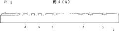
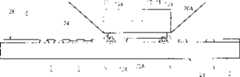
下面结合图4至9介绍MCM1的制造方法。图4至7分别是描述MCM的制造工艺的剖面图,图8和9分别是描述MCM的制造工艺的平面图。顺便提及,图4-7中省略了剖面的剖面线,以便于观察附图。The manufacturing method of the MCM1 will be described below with reference to FIGS. 4 to 9 . 4 to 7 are cross-sectional views describing the manufacturing process of the MCM, respectively, and FIGS. 8 and 9 are plan views describing the manufacturing process of the MCM, respectively. Incidentally, hatching of the sections is omitted in FIGS. 4-7 for ease of viewing the drawings.
关于本实施例,下面介绍在压焊安装电子元件的安装或封装后,安装焊接电子元件的实施例。Regarding this embodiment, an embodiment in which electronic components are mounted and soldered after mounting or packaging of the pressure-bonded mounted electronic components will be described below.
首先制备压焊安装电子元件(对应于控制芯片10、存储芯片12、缓冲芯片14和运算或算术芯片16)和焊接电子元件(对应于片式电容器17和18,片式电阻器19),并制备图4(A)所示的布线板2。接线柱焊盘11已形成于控制芯片10、存储芯片12、缓冲芯片14和运算芯片16的相应电极焊盘上。First prepare the pressure-bonded mounting electronic components (corresponding to the
然后,如图4(B)所示,利用涂敷或粘附工具(粘附头)25,将片状各向异性导电树脂膜20A从敷带(cover tape)23上转移到布线板2的一个主表面的相应控制芯片安装或装载区上。如图5(A)所示,将各向异性导电树脂膜20A设置在布线板2的一个主表面2X的相应控制芯片安装区。可以采用例如将大量导电颗粒混合于热固性环氧树脂得到的各向异性导电树脂膜20A。Then, as shown in FIG. 4(B), using a coating or sticking tool (adhesive head) 25, the sheet-like anisotropic
然后,如图5(B)所示,将相应的控制芯片10设置在布线板2的一个主表面2X的相应控制芯片安装区上,两者间夹有各向异性导电树脂膜20A。控制芯片10设置成其电路形成表面10X面对布线板2的一个主表面2X。利用芯片装载器的输运夹头,将控制芯片10从存储盘送到布线板2的一个主表面2X的控制芯片安装区。Then, as shown in FIG. 5(B), the
然后,如图6(A)所示,利用热压焊头26A,热压焊控制芯片10,从而连接接线柱凸点11与布线板2的相应连接部分3。然后,保持其热压焊状态直到各向异性导电树脂膜20A固化。各向异性导电树脂膜20A熔化一次,然后固化。于是,如图6(B)所示,控制芯片10通过固化的各向异性导电树脂20粘合并固定到布线板2上。控制芯片10的电极焊盘10a压焊到布线板2的相应连接部分3上,从而通过接线柱凸点11和大量混合到各向异性导电树脂20中的部分导电颗粒,电连接到布线板2的连接部分3。按本工艺,芯片的热压焊利用夹在控制芯片10和热压焊头26A之间的特氟隆片24进行。Then, as shown in FIG. 6(A), the
然后,利用类似于控制芯片10的方法,将每个存储芯片12设置在布线板2的一个主表面2X的相应存储芯片安装区。然后,利用类似于控制芯片10的方法,将每个缓冲芯片14设置在布线板2的一个主表面2X的相应缓冲芯片安装区。之后,利用类似于控制芯片10的方法,将每个运算芯片16设置在布线板2的一个主表面2X的相应运算芯片安装区。于是,如图8所示,将压焊安装或封装的元件设置在布线板2的一个主表面2X上。Then, each
当在压焊安装电子元件的安装之前,安装比压焊安装电子元件封装后高度大的焊接电子元件时,用于热压焊压焊安装电子元件的热压焊头26A变得容易接触已安装的焊接元件。因此,需要加宽每个焊接元件与相应的压焊安装电子元件间的间隔。然而,像本实施例一样,在焊接电子元件之前,安装压焊安装电子元件,可以基本消除热压焊头26A接触焊接元件的问题。因此,可以使焊接电子元件与相应的压焊安装电子元件间的间隔变窄。When mounting a soldered electronic component having a larger height than the packaged height of the pressure-soldered mounted electronic component before mounting of the press-soldered mounted electronic component, the
另外,在本实施例中,在180℃和20秒的条件下,进行各向异性导电树脂膜20A的固化。在预先将布线板2的温度设置到65℃后,利用加热到235℃的热压焊头26A,进行此时的加热。当与该热压焊工艺条件相比,在200℃和10秒的条件下,固化各向异性导电树脂膜20A,以进一步提高生产率时,需要将热压焊头26A的设定温度提供到265℃,同时布线板2的温度保持在65℃。In addition, in the present embodiment, curing of the anisotropic
当热压焊工艺的处理温度高于用作焊膏材料21A的焊料的熔点(例如,183℃)时,如果在压焊安装电子元件之前,安装焊接电子元件,每个焊接元件的焊料会由于热压焊工艺期间的热而熔化。当具休采用其尺寸可以覆盖焊接电子元件的安装区的热压焊头26A时,甚至在每个焊接电子元件的安装后高度高于或低于每个压焊安装电子元件的安装后高度的情况下,焊料也会熔化,因此,会引起例如遗漏每个焊接电子元件的问题。然而,当象本实施例一样,在焊接电子元件前安装压焊安装电子元件时,热压焊工艺期间的热处理没有对焊接电子元件产生不良影响的危险。另外,熔化焊膏材料21A的工艺期间的热在对已固化的各向异性导电树脂20产生不良影响方面也几乎没有危险。所以,有益的效果是由于在焊接电子元件之前,安装压焊安装电子元件,甚至可用于热压焊大芯片的大热压焊头26A,以及可以一起热压焊多个芯片的工艺也可以用于热压焊小芯片的工艺。When the processing temperature of the thermocompression bonding process is higher than the melting point (for example, 183° C.) of the solder used as the
当希望一起热压焊多个压焊安装电子元件,以提高生产率时,需要采用大于压焊安装电子元件的热压焊头。如果这种情况下,大高度的焊接电子元件存在于压焊头范围内,很难一起热压焊它们。然而,在焊接电子元件之前安装压焊安装电子元件,可以一起热压焊多个压焊安装电子元件。When it is desired to thermocompression-bond a plurality of pressure-bond-mounted electronic components together to increase productivity, it is necessary to use a thermocompression-bonding head that is larger than the pressure-bond-mounted electronic components. If in this case, soldered electronic components with a large height exist within the range of the bonding head, it is difficult to thermocompress them together. However, by mounting the press-bond-mounted electronic components before soldering the electronic components, a plurality of press-bond-mounted electronic components may be thermally pressure-bonded together.
当象本实施例所介绍的一样,采用至少大于压焊安装电子元件的热压焊头26A时,特氟隆片24可以夹在每个压焊安装电子元件和热压焊头26A之间,以防止热压焊头26A由于向着每个压焊安装电子元件的外围延伸的各向异性导电树脂20而被污染。When, as described in the present embodiment, when adopting at least a
然后,在布线板2的一个主表面2X上,在每个电极焊盘4上施加焊膏材料21A。利用分散法进行焊膏材料21A的施加,将焊膏材料21A从细喷嘴27中排出,施加于每个电极焊盘上,如图7(A)所示。关于焊膏材料21A,可以采用至少混合和捏和细焊料颗粒和焊剂得到的焊膏材料。在本实施例中,例如,可以采用混合和捏和成分为37wt%Pb-63wt%Sn的焊料颗粒得到的焊膏材料。顺便提及,焊剂可以包括松香、活性材料和有机溶剂等。Then, on one
然后,如图7(B)所示,在布线板2的一个主表面2X的相应电极焊盘4上,设置片式电容器17和18及片式电阻器19,两者间夹有焊膏材料21A。之后,进行热处理,以熔化焊膏材料21A,从而如图3所示,布线板2上的电极焊盘4和片式电容器17的电极17A通过焊料21彼此电和机械连接,布线板2上的电极焊盘4及片式电容器18和片式电阻器19的电极也按类似于片式电容器17的方式,通过焊料彼此电和机械连接。于是,如图9所示,焊接电子元件设置在布线板2的一个主表面2X上。Then, as shown in FIG. 7(B), on the corresponding
在熔化焊膏材料21A的过程中,每个焊接电子元件的外围被焊膏材料21A中包含的焊剂成分污染。然而,在焊接电子元件之前,安装压焊安装电子元件,可以防止与压焊安装电子元件连接的布线板2的各连接部分3被焊剂成分污染。In the process of melting the
上述实施例具有以下有益效果。The above embodiments have the following beneficial effects.
(1)在压焊安装电子元件之前,安装或封装与压焊安装电子元件相比安装后高度大的焊接电子元件。于是,由于可以基本上消除热压焊头26A与焊接电子元件接触,所以可以使焊接电子元件和压焊安装电子元件间的间隔变窄。结果,可以减小MCM1的尺寸。(1) Before pressure-welding mounting electronic components, mounting or packaging soldered electronic components having a larger post-mount height than pressure-bonding mounting electronic components. Thus, since the contact of the
由于在焊接电子元件之前实现或封装压焊安装电子元件,所以甚至是热压焊每个小芯片,也可以采用能够用于热压焊大芯片的工艺和一起热压焊多个芯片的工艺的大热压焊头26A。Since the press-bond mount electronic components are realized or packaged before the electronic components are soldered, even thermocompression bonding of each small chip can be performed using a process that can be used for thermocompression bonding of large chips and a process of thermocompression bonding of multiple chips together.
由于可以一起热压焊多个压焊安装电子元件,所以可以提高MCM1的生产率。The productivity of the MCM1 can be improved because multiple pressure-bonded mounted electronic components can be thermally pressure-bonded together.
当采用至少大于压焊安装电子元件的热压焊头26A时,可以在压焊安装电子元件和热压焊头26A之间夹入特氟隆片24,以防止热压焊头26A被向每个压焊安装电子元件外围延伸的各向异性导电树脂20污染。于是,可以提高MCM1的生产率。When adopting the
在焊接电子元件之前,安装压焊安装电子元件,可以防止与压焊安装电子元件连接的布线板2的各连接部分3被焊剂成分污染。结果,可以提高MCM1的生产率。By mounting the pressure-bonding mounted electronic components before soldering the electronic components, each
(2)利用分散法施加焊膏材料21A。于是,由于甚至在安装了压焊安装电子元件后,也可以将焊膏材料21A施加到布线板2的电极焊盘4上,所以甚至在安装了压焊安装电子元件后,也可以安装或封装焊接电子元件。(2) The
甚至可以利用凸凹掩模,利用丝网印刷法实施安装了压焊安装电子元件后的焊膏材料21A的施加。然而,这种情况下,很难邻近(约5mm以下)压焊安装电子元件设置每个焊接电子元件。因此,利用分散法施加焊膏材料的优点在于可以减小MCM1的尺寸。另一方面,当象焊接电子元件一样安装例如多管脚BGA、CSP、QFP和QFN型等半导体器件时,施加焊膏材料的点数增加。因此,无法利用分散法施加焊膏材料。当封装或实现这种多管脚半导体器件时,有利的是利用凸凹掩模,利用丝网印刷法施加焊膏材料。Even application of the
作为第二实施例,下面介绍制造MCM时,在安装了焊接安装的元件后,完成压焊安装元件的实施例。As a second embodiment, an embodiment in which the pressure-bonded mounted components are completed after mounting the solder-mounted components when manufacturing the MCM will be described below.
图10至15分别是描述本发明的第二实施例MCM的制造方法的剖面图。图16和17分别是本发明第二实施例的MCM制造方法的平面图。顺便提及,图10-15中省略了剖面的剖面线,以便于观察附图。10 to 15 are respectively cross-sectional views describing the manufacturing method of the MCM of the second embodiment of the present invention. 16 and 17 are respectively plan views of an MCM manufacturing method according to a second embodiment of the present invention. Incidentally, hatching of the sections is omitted in FIGS. 10-15 to facilitate viewing of the drawings.
首先,制备压焊安装部件或元件(控制芯片10,存储芯片12,缓冲芯片14和算术或运算芯片16)和焊接安装的部件或元件(片式电容器17和18,片式电阻器19)。另外,制备图10(A)所示的布线板2。在控制芯片10、存储芯片12、缓冲芯片14和运算芯片16的相应电极焊盘上形成接线柱凸点11。First, pressure-bonding mounted parts or elements (
然后,在布线板2的一个主表面2X上设置丝网掩模28。丝网掩模28在与布线板2上的各焊盘4相反的位置处具有孔或开口。Then, a
然后,在丝网掩模28的一个表面上施加半固态焊膏材料(膏状焊料)21A。关于焊膏材料21A,可以采用通过至少混合和捏和细焊料颗粒和焊剂得到的焊膏材料。本实施例中,采用例如混合和捏和每个成分都为37(wt%)铅(Pb)-63(wt%)锡(Sn)的焊料颗粒得到的焊膏材料。顺便提及,焊剂可以包括松香、活性材料和有机溶剂等。Then, a semi-solid solder paste material (cream solder) 21A is applied on one surface of the
然后,如图10(B)所示,刮板29沿丝网掩模28的一个表面滑动,以便将焊膏材料21A填入丝网掩模28的开口28A中,并去掉额外的焊膏材料21A。刮板29滑动几次。然后,除掉丝网掩模28,通过丝网印刷法使焊膏材料21A施加到布线板2的各电极焊盘4上,如图11(A)所示。以此方式,利用丝网印刷法,将焊膏材料21A一起施加到布线板2的各电极焊盘4上,与利用分散法等,将焊膏材料21A施加到各电极焊盘4上的情况相比,有利于例如多管脚BGA、CSP、QFP和QFN型等半导体器件的安装。Then, as shown in FIG. 10(B), the
然后,如图11(B)所示,在布线板2的一个主表面2X的相应电极焊盘4上,设置片式电容器17和18及片式电阻器19,两者间夹有焊膏材料21A。之后,进行热处理,以熔化焊膏材料21A,从而如图12(A)所示,布线板2上的电极焊盘4和片式电容器17的电极17A通过焊料21彼此电和机械连接,布线板2上的电极焊盘4及片式电容器18和片式电阻器19的电极也按类似于片式电容器17的方式,通过焊料21彼此电和机械连接。于是,如图16所示,焊接电子元件设置在布线板2的一个主表面2X上。Then, as shown in FIG. 11(B), on the corresponding
然后,如图12(B)所示,在安装压焊安装元件之前,用等离子体P清洗布线板2的各连接部分3(等离子体清洗)。这种等离子体清洗可以很好地去除由于焊膏材料21A中的焊剂成分造成的污染,防止接线柱焊盘11和布线板2的各连接部分3间的连接失效。Then, as shown in FIG. 12(B), each connecting
然后,如图13(A)所示,利用涂敷头或粘附头25,将片状各向异性导电树脂膜20A从敷带23转移到布线板2的一个主表面的相应控制芯片安装或装载区。如图13(B)所示,在布线板2的一个主表面2X的相应控制芯片安装区上,设置各向异性导电树脂膜20A。可以采用例如将大量导电颗粒混合到环氧热固性环氧树脂中得到各向异性导电树脂膜20A。Then, as shown in FIG. 13(A), the sheet-like anisotropic
然后,如图14(A)所示,将控制芯片10设置在布线板2的一个主表面2X的相应控制芯片安装区上,两者间夹有各向异性导电树脂膜20A。控制芯片10设置成使其电路形成表面10X面对布线板2的一个主表面2X。利用芯片装载器的输运夹头,将控制芯片10从存储盘送到布线板2的一个主表面2X的控制芯片安装区。Then, as shown in FIG. 14(A), the control chips 10 are disposed on the corresponding control chip mounting regions of the one
然后,如图14(B)所示,利用热压焊头26B,热压焊控制芯片10,从而连接接线柱凸点11与布线板2的相应连接部分3。然后,保持其热压焊状态直到各向异性导电树脂膜20A固化。各向异性导电树脂膜20A熔化一次,然后固化。于是,如图15所示,控制芯片10通过固化的各向异性导电树脂20粘合并固定到布线板2上。控制芯片10的电极焊盘10a压焊到布线板2的相应连接部分3上,从而通过接线柱凸点11和大量混合到各向异性导电树脂20中的部分导电颗粒,电连接到布线板2的相应连接部分3。Then, as shown in FIG. 14(B), the
然后,利用类似于控制芯片10的方法,将每个存储芯片12设置在布线板2的一个主表面2X的相应存储芯片安装区。然后,利用类似于控制芯片10的方法,将每个缓冲芯片14设置在布线板2的一个主表面2X的相应缓冲芯片安装区。之后,利用类似于控制芯片10的方法,将每个运算芯片16设置在布线板2的一个主表面2X的相应运算芯片安装区。于是,如图15和17所示,将压焊安装或封装的元件设置在布线板2的一个主表面2X上。Then, each
当在压焊安装电子元件的安装之前,安装焊接电子元件时,需要采用小到热压焊头26A不影响焊接电子元件的程度的热压焊头26B。由于采用热压焊头26B的头表面小于将热压焊的压焊安装电子元件的压焊头,可以防止热压焊头26B被向压焊安装电子元件外围延伸的各向异性导电树脂20污染。When mounting and soldering electronic components prior to mounting of the pressure-bonding mounted electronic components, it is necessary to use the
另外,由于所有接线柱凸点的上部被热压焊头26B的头表面覆盖,热压焊头26B的头表面小于压焊安装电子元件,热压焊头26B的表面的外围设定成在平面布局中位于接线柱凸点和压焊安装电子元件的外围之间。因此,热压焊头26B所加的热和压力可以更均匀地加于所有接线柱凸点上。In addition, since the tops of all the stud bumps are covered by the head surface of the thermocompression
上述实施例具有以下有益效果。The above embodiments have the following beneficial effects.
(1)由于在压焊安装电子元件之前安装焊接电子元件,可以根据标准丝网印刷法施加焊膏材料21A,所以与利用凸凹掩模,利用丝网印刷法,施加焊膏材料的情况相比,可以减小MCM的尺寸。另外,与利用分散法施加焊膏材料21A的情况相比,可以提高MCM的生产率。(1) Since the soldering electronic components are mounted and soldered before the electronic components are mounted by pressure bonding, the
(2)由于采用小于本实施例中要热压焊每个压焊安装电子元件的热压焊头26B的头表面,其中,在压焊安装电子元件之前安装焊接电子元件,所以,可以防止热压焊头26B被向压焊安装电子元件的外围延伸的各向异性导电树脂20污染。所以,可以提高生产率。(2) Since the head surface of the
(3)在压焊安装电子元件之前,实现焊接电子元件的实施例中,热压焊头26B的头表面的外围设定成位于接线柱凸点和每个压焊安装电子元件之间。因此,热压焊头26B所加的所有热和压力都可以更均匀地加于所有接线柱凸点上。(3) In an embodiment where soldering of the electronic components is performed before the electronic components are bonded, the outer periphery of the head surface of the thermocompression
(4)由于在安装每个压焊安装电子元件之前,可以通过等离子体屏蔽(plasma screening)清洗被焊膏材料21A中的焊剂等污染的布线板2的连接部分3,所以可以控制或限制压焊安装电子元件和布线板2的连接部分3间的电连接失效。所以,可以提高MCM的成品率。(4) Since the
(5)采用小于要热压焊的每个压焊安装电子元件的热压焊头,从而可避免已安装的焊接电子元件与热压焊头间的接触。(5) Using a thermocompression head smaller than each of the thermocompression mounted electronic components to be thermocompression bonded, contact between the mounted soldered electronic components and the thermocompression head can be avoided.
顺便提及,第一和第二实施例分别介绍了接线柱凸点用作形成于半导体芯片的电极焊盘上的突起电极的例子。然而,本发明不限于此。例如,可以采用具有Pb-Sn成分的焊料凸点。然而,也可以采用这样的焊料凸点,即包括熔点高于每个焊接电子元件安装时的焊料熔化温度和每个压焊安装电子元件安装时的热压焊温度的材料。Incidentally, the first and second embodiments respectively describe examples in which stud bumps are used as protruding electrodes formed on electrode pads of a semiconductor chip. However, the present invention is not limited thereto. For example, solder bumps having a Pb-Sn composition may be used. However, it is also possible to use a solder bump including a material having a melting point higher than the melting temperature of solder when each soldered electronic component is mounted and the thermocompression bonding temperature when each bonding electronic component is mounted.
尽管第一和第二实施例分别介绍了夹在压焊安装电子元件的电极焊盘与布线板的相应连接部分间的突起电极,预先形成于压焊安装电子元件的相应电极焊盘上的例子,但突起电极可预先形成于布线板的连接部分上。Although the first and second embodiments respectively describe the protruding electrodes sandwiched between the electrode pads of the pressure-bonding mounted electronic components and the corresponding connection portions of the wiring board, the examples in which the electrodes are preliminarily formed on the corresponding electrode pads of the pressure-bonded mounted electronic components , but the protruding electrodes may be formed in advance on the connection portion of the wiring board.
另外,尽管第一和第二实施例分别介绍了采用片状导电树脂作为将每个压焊安装电子元件焊接和固定于布线板上的焊接树脂的例子,但本发明不限于此。例如,可以采用膏状各向异性导电树脂(ACP)和片状非导电树脂(NCF)。In addition, although the first and second embodiments respectively describe examples in which a sheet-like conductive resin is used as the soldering resin for soldering and fixing each of the press-bond mounted electronic components to the wiring board, the present invention is not limited thereto. For example, paste-like anisotropic conductive resin (ACP) and sheet-like non-conductive resin (NCF) can be used.
作为第三实施例,下面介绍其上附有散热器的MCM。As a third embodiment, an MCM with a heat sink attached thereto will be described below.
图18是本发明第三实施例的MCM的剖面图,图19和20分别是图18中所示MCM的设计图。顺便提及,图18中省略了剖面的剖面线,以便于观察。18 is a cross-sectional view of an MCM according to a third embodiment of the present invention, and FIGS. 19 and 20 are design views of the MCM shown in FIG. 18, respectively. Incidentally, hatching of the section is omitted in FIG. 18 for ease of observation.
如图18至20所示,根据本发明的MCM构成为具有导热片30和散热器31。导热片30例如由弹性硅橡胶形成,散热器31例如由铝构成的平板形成。As shown in FIGS. 18 to 20 , the MCM according to the present invention is constituted with a
导热片30的形状构成为使之与每个压焊安装电子元件的背面接触,而不与片式电容器17和18接触。将具有这种形状的导热片30安装到每个压焊安装电子元件的背面,将散热器31安装到导热片30上,从而可以利用导热片30的厚度,实现压焊安装电子元件与每个片式电容器17和18间的垂直间隔差。因此,片式电容器17和18的高度大不会影响压焊安装电子元件与导热片30间的接触,如图21所示。所以,压焊安装电子元件工作产生的热可以有效地传送到导热片30,因此,可以提高MCM的耗散。The
散热器31形成为覆盖多个压焊安装电子元件和多个焊接电子元件,其平面尺寸大于导热片30,所以散热器31的面积增大,于是可以提高MCM的耗散。The
另外,导热片30的形状形成为使之与每个片式电阻器19A接触。是由于设置于片式电阻器19A两侧的控制芯片10和每个存储芯片12的高度皆为0.4mm,而片式电阻器19A的高度为0.45mm,两者间垂直高度差等于能够容许导热片30形变的程度。由于以此方式,在导热片30的应用或粘附区内,在焊接元件间选择安装后高度较低的元件的位置,也可以有效地利用相邻压焊安装电子元件间的面积,所以可以减小MCM的尺寸。In addition, the
尽管利用例示的实施例对本发明人所做的上述发明做了介绍,但本发明不限于这些实施例。无需说,在不脱离本发明的本质的情况下,可以对其做出各种变化。下面简单介绍一下本申请所公开的发明的有益效果:Although the above invention made by the present inventors has been described using illustrative embodiments, the present invention is not limited to these embodiments. It goes without saying that various changes can be made thereto without departing from the essence of the present invention. Briefly introduce the beneficial effects of the invention disclosed in this application below:
根据本发明,可以提高电子器件的生产率。According to the present invention, the productivity of electronic devices can be improved.
根据本发明,可以减小电子器件的尺寸。According to the present invention, electronic devices can be reduced in size.
根据本发明,可以增强电子器件的耗散。According to the present invention, the dissipation of electronic devices can be enhanced.
Claims (21)
Applications Claiming Priority (2)
| Application Number | Priority Date | Filing Date | Title |
|---|---|---|---|
| JP2000263864AJP2002076589A (en) | 2000-08-31 | 2000-08-31 | Electronic device and manufacturing method thereof |
| JP263864/2000 | 2000-08-31 |
Publications (2)
| Publication Number | Publication Date |
|---|---|
| CN1340851Atrue CN1340851A (en) | 2002-03-20 |
| CN1291467C CN1291467C (en) | 2006-12-20 |
Family
ID=18751356
Family Applications (1)
| Application Number | Title | Priority Date | Filing Date |
|---|---|---|---|
| CNB011252278AExpired - Fee RelatedCN1291467C (en) | 2000-08-31 | 2001-08-31 | Electronic device and its manufacture method |
Country Status (6)
| Country | Link |
|---|---|
| US (4) | US6553660B2 (en) |
| JP (1) | JP2002076589A (en) |
| KR (1) | KR20020018133A (en) |
| CN (1) | CN1291467C (en) |
| SG (1) | SG101995A1 (en) |
| TW (1) | TW523839B (en) |
Cited By (4)
| Publication number | Priority date | Publication date | Assignee | Title |
|---|---|---|---|---|
| CN100435301C (en)* | 2003-09-19 | 2008-11-19 | 株式会社瑞萨科技 | Method for manufacturing semiconductor integrated circuit device |
| CN103084694A (en)* | 2011-10-21 | 2013-05-08 | 株式会社工房Pda | Hot pressure welding head, bonding apparatus, bonding method and junction structure of thin line and terminal |
| CN112968109A (en)* | 2020-11-27 | 2021-06-15 | 重庆康佳光电技术研究院有限公司 | Driving back plate and manufacturing method thereof |
| CN118692883A (en)* | 2023-06-02 | 2024-09-24 | 台湾积体电路制造股份有限公司 | Method of forming a joint assembly and apparatus for forming a joint assembly |
Families Citing this family (28)
| Publication number | Priority date | Publication date | Assignee | Title |
|---|---|---|---|---|
| US6305076B1 (en)* | 2000-01-21 | 2001-10-23 | Cypress Semiconductor Corp. | Apparatus for transferring a plurality of integrated circuit devices into and/or out of a plurality of sockets |
| JP3767474B2 (en)* | 2001-01-15 | 2006-04-19 | セイコーエプソン株式会社 | Display device and manufacturing method thereof |
| JP4105409B2 (en)* | 2001-06-22 | 2008-06-25 | 株式会社ルネサステクノロジ | Multi-chip module manufacturing method |
| US7714432B2 (en)* | 2002-07-26 | 2010-05-11 | Intel Corporation | Ceramic/organic hybrid substrate |
| US7145234B2 (en)* | 2004-01-15 | 2006-12-05 | Via Technologies, Inc. | Circuit carrier and package structure thereof |
| US7167375B2 (en)* | 2004-01-16 | 2007-01-23 | Motorola, Inc. | Populated printed wiring board and method of manufacture |
| US20050205292A1 (en)* | 2004-03-18 | 2005-09-22 | Etenna Corporation. | Circuit and method for broadband switching noise suppression in multilayer printed circuit boards using localized lattice structures |
| GB2412790B (en)* | 2004-04-02 | 2007-12-05 | Univ City Hong Kong | Process for assembly of electronic devices |
| WO2006001087A1 (en)* | 2004-06-29 | 2006-01-05 | Renesas Technology Corp. | Semiconductor device |
| US20060107523A1 (en)* | 2004-11-24 | 2006-05-25 | Trw Inc. | Method of making a printed circuit board |
| US7916263B2 (en)* | 2004-12-02 | 2011-03-29 | Semiconductor Energy Laboratory Co., Ltd. | Display device |
| JP2006303173A (en)* | 2005-04-20 | 2006-11-02 | Mitsubishi Electric Corp | Circuit board device and manufacturing method thereof |
| US20070065964A1 (en)* | 2005-09-22 | 2007-03-22 | Yinon Degani | Integrated passive devices |
| CN1945822B (en)* | 2005-10-07 | 2012-05-23 | 日立麦克赛尔株式会社 | Semiconductor device, semiconductor module and semiconductor module producing method |
| US7637415B2 (en) | 2005-10-31 | 2009-12-29 | General Electric Company | Methods and apparatus for assembling a printed circuit board |
| US7871865B2 (en)* | 2007-01-24 | 2011-01-18 | Analog Devices, Inc. | Stress free package and laminate-based isolator package |
| JP4454673B2 (en)* | 2008-08-01 | 2010-04-21 | 株式会社新川 | Metal nano ink, method for producing the same, die bonding method and die bonding apparatus using the metal nano ink |
| JP5509738B2 (en) | 2008-09-30 | 2014-06-04 | デクセリアルズ株式会社 | Acrylic insulating adhesive |
| KR101044008B1 (en)* | 2008-10-08 | 2011-06-24 | 주식회사 하이닉스반도체 | Flexible semiconductor package and manufacturing method thereof |
| EP2453726A1 (en)* | 2009-06-01 | 2012-05-16 | Sumitomo Electric Industries, Ltd. | Connection method, connection structure, and electronic device |
| JP2012028513A (en)* | 2010-07-22 | 2012-02-09 | Elpida Memory Inc | Semiconductor device and manufacturing method of the same |
| KR101940237B1 (en)* | 2012-06-14 | 2019-01-18 | 한국전자통신연구원 | Method for Manufacturing Solder on Pad on Fine Pitch PCB Substrate and Flip Chip Bonding Method of Semiconductor Using The Same |
| TW201436665A (en)* | 2013-03-07 | 2014-09-16 | Delta Electronics Inc | Automatic processes and structures for disposing cushions of circuit board |
| JP2015015442A (en) | 2013-07-08 | 2015-01-22 | 三菱電機株式会社 | Semiconductor device |
| TWI582905B (en)* | 2016-01-07 | 2017-05-11 | 晨星半導體股份有限公司 | Chip package structure and manufacturing method thereof |
| KR101908915B1 (en) | 2016-06-10 | 2018-10-18 | 크루셜머신즈 주식회사 | Reel to reel laser reflow method |
| JP2022125682A (en)* | 2021-02-17 | 2022-08-29 | レノボ・シンガポール・プライベート・リミテッド | Electronic substrate and electronic equipment |
| US20240147633A1 (en)* | 2021-12-27 | 2024-05-02 | Daiwa Co., Ltd. | Method for manufacturing wiring board or wiring board material |
Family Cites Families (29)
| Publication number | Priority date | Publication date | Assignee | Title |
|---|---|---|---|---|
| US4515304A (en)* | 1982-09-27 | 1985-05-07 | Northern Telecom Limited | Mounting of electronic components on printed circuit boards |
| FR2556550B1 (en)* | 1983-12-09 | 1987-01-30 | Lignes Telegraph Telephon | METHOD OF BRAZING ELECTRONIC COMPONENTS ON A PRINTED CIRCUIT AND HYBRID CIRCUIT OBTAINED BY THIS METHOD |
| US4761881A (en)* | 1986-09-15 | 1988-08-09 | International Business Machines Corporation | Single step solder process |
| US4872261A (en)* | 1987-12-11 | 1989-10-10 | Digital Equipment Corporation | Method of and apparatus for surface mounting electronic components onto a printed wiring board |
| DE3806738C1 (en)* | 1988-03-02 | 1989-09-07 | Espe Stiftung & Co Produktions- Und Vertriebs Kg, 8031 Seefeld, De | |
| JP2502663B2 (en)* | 1988-03-17 | 1996-05-29 | 松下電器産業株式会社 | Manufacturing method of printed wiring board |
| US4982376A (en)* | 1989-04-20 | 1991-01-01 | U.S. Philips Corporation | Method of mounting electrical and/or electronic components on a single-sided printed board |
| US4998342A (en)* | 1989-08-31 | 1991-03-12 | International Business Machines Corporation | Method of attaching electronic components |
| US4941255A (en)* | 1989-11-15 | 1990-07-17 | Eastman Kodak Company | Method for precision multichip assembly |
| JP2824148B2 (en)* | 1990-11-28 | 1998-11-11 | 富士通株式会社 | Work table for manufacturing double-sided wire bonding board assembly |
| US5155904A (en)* | 1991-04-03 | 1992-10-20 | Compaq Computer Corporation | Reflow and wave soldering techniques for bottom side components |
| US5604978A (en)* | 1994-12-05 | 1997-02-25 | International Business Machines Corporation | Method for cooling of chips using a plurality of materials |
| US5754401A (en)* | 1996-02-16 | 1998-05-19 | Sun Microsystems, Inc. | Pressure compliantly protected heatsink for an electronic device |
| DE69709978T2 (en)* | 1996-04-30 | 2002-11-21 | Denki Kagaku Kogyo K.K., Tokio/Tokyo | Heat dissipating spacers for electronic devices |
| US5678304A (en)* | 1996-07-24 | 1997-10-21 | Eastman Kodak Company | Method for manufacturing double-sided circuit assemblies |
| US5812374A (en)* | 1996-10-28 | 1998-09-22 | Shuff; Gregg Douglas | Electrical circuit cooling device |
| US5729896A (en)* | 1996-10-31 | 1998-03-24 | International Business Machines Corporation | Method for attaching a flip chip on flexible circuit carrier using chip with metallic cap on solder |
| US6144101A (en)* | 1996-12-03 | 2000-11-07 | Micron Technology, Inc. | Flip chip down-bond: method and apparatus |
| DE19651528B4 (en)* | 1996-12-11 | 2005-10-06 | Fraunhofer-Gesellschaft zur Förderung der angewandten Forschung e.V. | Chip arrangement and method for producing the same |
| JPH10270496A (en)* | 1997-03-27 | 1998-10-09 | Hitachi Ltd | Electronic device, information processing device, semiconductor device, and semiconductor chip mounting method |
| US5990564A (en)* | 1997-05-30 | 1999-11-23 | Lucent Technologies Inc. | Flip chip packaging of memory chips |
| JP3982876B2 (en)* | 1997-06-30 | 2007-09-26 | 沖電気工業株式会社 | Surface acoustic wave device |
| JP3687280B2 (en)* | 1997-07-02 | 2005-08-24 | 松下電器産業株式会社 | Chip mounting method |
| JP3109477B2 (en)* | 1998-05-26 | 2000-11-13 | 日本電気株式会社 | Multi-chip module |
| KR100514559B1 (en)* | 1998-07-01 | 2005-09-13 | 세이코 엡슨 가부시키가이샤 | Semiconductor device, method of manufacture thereof, circuit board, and electronic device |
| DE19924289A1 (en)* | 1999-05-27 | 2000-12-07 | Siemens Ag | Electronic circuit module with flexible intermediate layer between electronic components and heat-sink |
| JP2001210763A (en)* | 2000-01-27 | 2001-08-03 | Mitsubishi Electric Corp | Semiconductor module device |
| US6212074B1 (en)* | 2000-01-31 | 2001-04-03 | Sun Microsystems, Inc. | Apparatus for dissipating heat from a circuit board having a multilevel surface |
| US6673690B2 (en)* | 2000-04-27 | 2004-01-06 | Siliconware Precision Industries Co., Ltd. | Method of mounting a passive component over an integrated circuit package substrate |
- 2000
- 2000-08-31JPJP2000263864Apatent/JP2002076589A/enactivePending
- 2001
- 2001-08-08SGSG200104762Apatent/SG101995A1/enunknown
- 2001-08-13TWTW090119799Apatent/TW523839B/ennot_activeIP Right Cessation
- 2001-08-23USUS09/935,170patent/US6553660B2/ennot_activeExpired - Fee Related
- 2001-08-30KRKR1020010052729Apatent/KR20020018133A/ennot_activeCeased
- 2001-08-31CNCNB011252278Apatent/CN1291467C/ennot_activeExpired - Fee Related
- 2002
- 2002-05-23USUS10/152,839patent/US20020135986A1/ennot_activeAbandoned
- 2003
- 2003-02-04USUS10/357,221patent/US6722028B2/ennot_activeExpired - Fee Related
- 2004
- 2004-03-02USUS10/790,057patent/US7015070B2/ennot_activeExpired - Fee Related
Cited By (5)
| Publication number | Priority date | Publication date | Assignee | Title |
|---|---|---|---|---|
| CN100435301C (en)* | 2003-09-19 | 2008-11-19 | 株式会社瑞萨科技 | Method for manufacturing semiconductor integrated circuit device |
| CN103084694A (en)* | 2011-10-21 | 2013-05-08 | 株式会社工房Pda | Hot pressure welding head, bonding apparatus, bonding method and junction structure of thin line and terminal |
| CN103084694B (en)* | 2011-10-21 | 2016-08-03 | 株式会社工房Pda | The connecting structure of hot-pressing welding head and engagement device and joint method and fine rule and terminal |
| CN112968109A (en)* | 2020-11-27 | 2021-06-15 | 重庆康佳光电技术研究院有限公司 | Driving back plate and manufacturing method thereof |
| CN118692883A (en)* | 2023-06-02 | 2024-09-24 | 台湾积体电路制造股份有限公司 | Method of forming a joint assembly and apparatus for forming a joint assembly |
Also Published As
| Publication number | Publication date |
|---|---|
| US20020023342A1 (en) | 2002-02-28 |
| US20030135996A1 (en) | 2003-07-24 |
| US20040166608A1 (en) | 2004-08-26 |
| JP2002076589A (en) | 2002-03-15 |
| US6553660B2 (en) | 2003-04-29 |
| US6722028B2 (en) | 2004-04-20 |
| US20020135986A1 (en) | 2002-09-26 |
| TW523839B (en) | 2003-03-11 |
| CN1291467C (en) | 2006-12-20 |
| KR20020018133A (en) | 2002-03-07 |
| US7015070B2 (en) | 2006-03-21 |
| SG101995A1 (en) | 2004-02-27 |
Similar Documents
| Publication | Publication Date | Title |
|---|---|---|
| CN1340851A (en) | Electronic device and its manufacture method | |
| CN1271712C (en) | Semiconductor device with heat sink exposed from sealing resin | |
| CN1154178C (en) | Semiconductor device, method of manufacturing the same, circuit board, and electronic device | |
| CN1161834C (en) | Semiconductor device and manufacturing method thereof | |
| CN1143375C (en) | Semiconductor device, method of manufacture, circuit board and electronic device | |
| CN1185698C (en) | Semiconductor device and manufacture method thereof, circuit board and electronic apparatus | |
| JP5085932B2 (en) | Mounted body and manufacturing method thereof | |
| CN1812077A (en) | Integrated circuit packaging structure and bottom filling process | |
| CN111384031B (en) | Packaging element and preparation method thereof | |
| CN1819133A (en) | Method for manufacturing semiconductor device and method for treating electrical connection portion | |
| CN1512580A (en) | Semiconductor device and manufacturing method thereof | |
| CN1427471A (en) | Semiconductor device | |
| US20170318661A1 (en) | Circuit board and on-board structure of semiconductor integrated circuit | |
| KR20020008004A (en) | Semiconductor device having heat spreader attached thereto and method of manufacturing the same | |
| JP4887997B2 (en) | Electronic component mounting method | |
| CN1638122A (en) | Method of manufacturing a semiconductor device | |
| CN103098191A (en) | Electronic-component mounted body, electronic component, and circuit board | |
| TWI332694B (en) | Chip package structure and process for fabricating the same | |
| KR102006637B1 (en) | Method Of Forming Bump And Semiconductor device including The Same | |
| CN1531043A (en) | Electronic device manufacturing method and chip carrier | |
| CN1481002A (en) | Method for manufacturing semiconductor device | |
| JP2010135501A (en) | Method of manufacturing semiconductor device | |
| JPH1050770A (en) | Semiconductor device and manufacturing method thereof | |
| CN1956177A (en) | Chip structure, chip packaging structure and technology | |
| CN1286158C (en) | Method of manufacturing semiconductor device and electronic device |
Legal Events
| Date | Code | Title | Description |
|---|---|---|---|
| C06 | Publication | ||
| PB01 | Publication | ||
| C10 | Entry into substantive examination | ||
| SE01 | Entry into force of request for substantive examination | ||
| C14 | Grant of patent or utility model | ||
| GR01 | Patent grant | ||
| C17 | Cessation of patent right | ||
| CF01 | Termination of patent right due to non-payment of annual fee | Granted publication date:20061220 Termination date:20090930 |