CN1334967A - Organic light emitting device - Google Patents
Organic light emitting deviceDownload PDFInfo
- Publication number
- CN1334967A CN1334967ACN99815945ACN99815945ACN1334967ACN 1334967 ACN1334967 ACN 1334967ACN 99815945 ACN99815945 ACN 99815945ACN 99815945 ACN99815945 ACN 99815945ACN 1334967 ACN1334967 ACN 1334967A
- Authority
- CN
- China
- Prior art keywords
- light emitting
- layer
- electrode layer
- organic
- emitting device
- Prior art date
- Legal status (The legal status is an assumption and is not a legal conclusion. Google has not performed a legal analysis and makes no representation as to the accuracy of the status listed.)
- Granted
Links
Images


Classifications
- H—ELECTRICITY
- H10—SEMICONDUCTOR DEVICES; ELECTRIC SOLID-STATE DEVICES NOT OTHERWISE PROVIDED FOR
- H10K—ORGANIC ELECTRIC SOLID-STATE DEVICES
- H10K59/00—Integrated devices, or assemblies of multiple devices, comprising at least one organic light-emitting element covered by group H10K50/00
- H10K59/80—Constructional details
- H10K59/805—Electrodes
- H—ELECTRICITY
- H10—SEMICONDUCTOR DEVICES; ELECTRIC SOLID-STATE DEVICES NOT OTHERWISE PROVIDED FOR
- H10K—ORGANIC ELECTRIC SOLID-STATE DEVICES
- H10K50/00—Organic light-emitting devices
- H10K50/10—OLEDs or polymer light-emitting diodes [PLED]
- H10K50/11—OLEDs or polymer light-emitting diodes [PLED] characterised by the electroluminescent [EL] layers
- H—ELECTRICITY
- H10—SEMICONDUCTOR DEVICES; ELECTRIC SOLID-STATE DEVICES NOT OTHERWISE PROVIDED FOR
- H10K—ORGANIC ELECTRIC SOLID-STATE DEVICES
- H10K50/00—Organic light-emitting devices
- H10K50/10—OLEDs or polymer light-emitting diodes [PLED]
- H10K50/14—Carrier transporting layers
- H10K50/16—Electron transporting layers
- H—ELECTRICITY
- H10—SEMICONDUCTOR DEVICES; ELECTRIC SOLID-STATE DEVICES NOT OTHERWISE PROVIDED FOR
- H10K—ORGANIC ELECTRIC SOLID-STATE DEVICES
- H10K50/00—Organic light-emitting devices
- H10K50/80—Constructional details
- H10K50/805—Electrodes
- H—ELECTRICITY
- H10—SEMICONDUCTOR DEVICES; ELECTRIC SOLID-STATE DEVICES NOT OTHERWISE PROVIDED FOR
- H10K—ORGANIC ELECTRIC SOLID-STATE DEVICES
- H10K2102/00—Constructional details relating to the organic devices covered by this subclass
- H10K2102/20—Metallic electrodes, e.g. using a stack of layers
- H—ELECTRICITY
- H10—SEMICONDUCTOR DEVICES; ELECTRIC SOLID-STATE DEVICES NOT OTHERWISE PROVIDED FOR
- H10K—ORGANIC ELECTRIC SOLID-STATE DEVICES
- H10K2102/00—Constructional details relating to the organic devices covered by this subclass
- H10K2102/301—Details of OLEDs
- H10K2102/351—Thickness
- Y—GENERAL TAGGING OF NEW TECHNOLOGICAL DEVELOPMENTS; GENERAL TAGGING OF CROSS-SECTIONAL TECHNOLOGIES SPANNING OVER SEVERAL SECTIONS OF THE IPC; TECHNICAL SUBJECTS COVERED BY FORMER USPC CROSS-REFERENCE ART COLLECTIONS [XRACs] AND DIGESTS
- Y10—TECHNICAL SUBJECTS COVERED BY FORMER USPC
- Y10S—TECHNICAL SUBJECTS COVERED BY FORMER USPC CROSS-REFERENCE ART COLLECTIONS [XRACs] AND DIGESTS
- Y10S428/00—Stock material or miscellaneous articles
- Y10S428/917—Electroluminescent
Landscapes
- Physics & Mathematics (AREA)
- Optics & Photonics (AREA)
- Electroluminescent Light Sources (AREA)
Abstract
Description
Translated fromChinese技术领域technical field
本发明涉及有机发光器件(OLEDs)和一种改善具有含本征缺陷的发光有机层的OLEDs的电流密度均匀性的方法。The present invention relates to organic light emitting devices (OLEDs) and a method for improving the current density uniformity of OLEDs having a light emitting organic layer containing intrinsic defects.
本发明也涉及一种有已构图的电极的有机发光器件。The invention also relates to an organic light emitting device having patterned electrodes.
背景技术Background technique
有机发光器件,如美国专利US5247190或美国专利US4539507(其内容引入本文作为参考)所述,在不同的显示应用中有更多可能的应用。根据一种方法,用透明的第一电极(阳极)例如铟-锡氧化物(ITO)覆盖玻璃或塑料衬底制造一个OLED。然后在最后一层一般是金属或合金的第二电极膜(阴极)形成之前淀积至少一层电致发光有机材料薄膜。Organic light emitting devices, as described in US Pat. No. 5,247,190 or US Pat. No. 4,539,507 (the contents of which are incorporated herein by reference), have more possible applications in different display applications. According to one method, an OLED is fabricated by covering a glass or plastic substrate with a transparent first electrode (anode), such as indium-tin oxide (ITO). Then at least one thin film of electroluminescent organic material is deposited before the final second electrode film (cathode) which is generally metal or alloy is formed.
在许多实际应用中,电致发光有机材料层有100nm数量级的厚度以保证一个实际的工作电压。它一般是通过旋涂技术淀积在第一电极上。如果该有机材料被与有机材料层的厚度尺寸同一数量级的微粒所污染,在形成的有机层中不仅这些微粒它们自己会带来缺陷,而且它们的存在还使在第一电极层表面上的有机材料流体的运动中断,从而导致微粒周围形成的有机层厚度变化,最坏时导致有机层中形成空洞,透过空洞下面的层(电极层)被暴露。In many practical applications, the electroluminescent organic material layer has a thickness on the order of 100 nm to ensure a practical operating voltage. It is typically deposited on the first electrode by spin-coating techniques. If the organic material is polluted by particles of the same order of magnitude as the thickness of the organic material layer, not only will these particles themselves bring defects in the formed organic layer, but their presence will also make the organic particles on the surface of the first electrode layer The movement of the material fluid is interrupted, which leads to a change in the thickness of the organic layer formed around the particle and, in the worst case, to the formation of voids in the organic layer through which the underlying layer (electrode layer) is exposed.
例如,有机材料固有的成膜性能较差,或者淀积之后通过物理损伤该有机层,而会在有机层内产生缺陷。For example, the inherent film-forming properties of organic materials are poor, or defects may be generated in the organic layer by physically damaging the organic layer after deposition.
图3表示一个典型的缺陷位置。电致发光有机层106通过旋涂被淀积在覆盖一层铟-锡氧化物(ITO)阳极层的玻璃衬底102上。大颗粒107的存在导致一个包含颗粒107本身和针孔111缺陷位置109。在电致发光有机层106上形成一阴极层110。Figure 3 shows a typical defect location. An electroluminescent organic layer 106 is deposited by spin coating on a glass substrate 102 covered with an indium-tin oxide (ITO) anode layer. The presence of large particles 107 results in a defect site 109 containing the particles 107 themselves and pinholes 111 . A cathode layer 110 is formed on the electroluminescent organic layer 106 .
图3表示这种局部缺陷可在器件工作过程中表现为电流异常(短路)即大部分电流开始停留在缺陷区域。这导致,尤其是器件的再现性问题,在点矩阵器件中这尤其是一个问题,因为它提供了另外的电流路径,从而导致错误的像素发光。Figure 3 shows that such a localized defect can manifest as an abnormal current (short circuit) during device operation, ie most of the current starts to stay in the defect area. This leads, inter alia, to device reproducibility problems, which is especially a problem in dot-matrix devices because it provides an additional current path leading to wrong pixels being illuminated.
为了防止这种缺陷,有机层的淀积一般在洁净室中进行,目的在于防止污染,一般在旋转之前对有机材料进行过滤除去大的微粒。然而,一般洁净室的微粒数量级下限为300nm,有机材料典型的仅是在450nm左右被过滤,因为排除更小尺寸的微粒需要更多的费用。To prevent such defects, the deposition of the organic layers is generally carried out in a clean room. In order to prevent contamination, the organic material is generally filtered to remove large particles before spinning. However, the lower limit of the order of magnitude of particles in a general clean room is 300nm, and organic materials are typically only filtered at around 450nm, because it costs more to exclude particles of smaller sizes.
因此发光有机材料仍将经常被与待淀积的有机层厚度有同样数量级尺寸的微粒所污染,如上所述,它将导致在形成的有机层中形成缺陷。而且,即使大颗粒的污染能被完全排除,缺陷仍然可出现在制造过程中,例如,因为有机材料本身固有的成膜特性差,或者因为在有机层淀积之后不经意造成的物理损伤。The light-emitting organic material will therefore still often be contaminated with particles of the same order of magnitude as the thickness of the organic layer to be deposited, which, as mentioned above, will lead to the formation of defects in the organic layer formed. Moreover, even if contamination by large particles can be completely excluded, defects can still occur during fabrication, for example, because of inherently poor film-forming properties of the organic material itself, or because of inadvertent physical damage after organic layer deposition.
已知的在器件的生产之后去除缺陷微粒的技术是用非常高的电流流经该器件,通过使这些缺陷蒸发而“烧掉”缺陷微粒。然而,该技术不能应用于所有的缺陷微粒,并且不能用来解决大的短路问题。而且,它未必能处理可以出现在器件的有效期内的问题,因此本发明的一个目的是减少有机发光器件中电流异常的问题。A known technique for removing defect particles after production of a device is to "burn off" the defect particles by evaporating the defects by passing a very high current through the device. However, this technique cannot be applied to all defect particles and cannot be used to solve large short circuits. Also, it does not necessarily deal with problems that may occur during the lifetime of the device, so it is an object of the present invention to reduce the problem of current abnormalities in organic light emitting devices.
有机发光器件(OLEDs),例如我们更早的美国专利US-A-5247190或Van Slyke等的US-A-4539507所描述,仅在阴极和阳极交迭处发出来自所述至少一个有机层的光,因此仅通过对电极构图,可以简单地获得像素和图形。高分辨率是容易获得的,其主要限制仅为阳极和阴极交迭区域即阳极和阴极的尺寸。一般是通过排列阳极和阴极作为垂直的行和列阵列,并且将至少一个有机层设于其间来制造点矩阵显示。Organic light emitting devices (OLEDs), such as those described in our earlier US-A-5247190 or US-A-4539507 by Van Slyke et al., emit light from said at least one organic layer only where the cathode and anode overlap , so pixels and patterns can be obtained simply by patterning the electrodes. High resolution is readily achievable, with the main limitation being only the anode and cathode overlap area, ie the size of the anode and cathode. Dot-matrix displays are generally fabricated by arranging anodes and cathodes as a vertical array of rows and columns, with at least one organic layer interposed therebetween.
低分辨率点矩阵显示也可以例如,通过在有作为阳极的铟-锡氧化物(ITO)线阵列的衬底上覆盖至少一层有机电致发光层制造。在所述至少一个有机层的另一侧设置包含垂直于那些阳极线阵列的线阵列的阴极。这些阴极线可以例如是用一个物理阴罩蒸发或溅射的铝线或铝基合金线。但是,阴罩并不是对于各种原因都理想。特别,当需要大面积和/或高分辨率显示时使用阴罩存在明显限制,为了制造这样的电极线阵列和其他大面积和/或高分辨率图形,通常不得不使用各种形式的光刻技术。Low-resolution dot-matrix displays can also be fabricated, for example, by overlaying at least one organic electroluminescent layer on a substrate with an array of indium-tin-oxide (ITO) lines as anode. On the other side of the at least one organic layer is arranged a cathode comprising an array of wires perpendicular to those of the anode wires. These cathode wires can be, for example, aluminum wires or aluminum-based alloy wires evaporated or sputtered with a physical shadow mask. However, shadow masks are not ideal for every reason. In particular, there are significant limitations to the use of shadow masks when large-area and/or high-resolution displays are required, and in order to fabricate such electrode line arrays and other large-area and/or high-resolution patterns, various forms of photolithography typically have to be used technology.
为了制造有效的和稳定并且有希望的电和光输出特性的OLEDs,必须经常多观注所有有机层和电极之间界面的设计和构造,这些界面的特殊重要性在于电荷载流子应该从电极被有效注入到至少一个有机层内这个事实。In order to fabricate efficient and stable OLEDs with promising electrical and light output properties, much attention must often be paid to the design and construction of the interfaces between all organic layers and electrodes. The particular importance of these interfaces is that charge carriers should be extracted from the electrodes. The fact that it is effectively injected into at least one organic layer.
光刻工艺用来制造电极图形,特别是这些图形在至少一个有机层顶部时在OLED显示中保持像素希望的电和光输出特性,考虑光刻工艺具有改变和潜在损坏有机层/电极界面和邻近区的危险并非不重要的。在光刻过程中的这些损坏可能由光刻胶,显影剂,蚀刻过程(干蚀或湿蚀刻,负型和正型工艺和蚀刻、剥离)或使用的溶剂所引起,应该注意这里,共轭聚合物通常溶解在有机溶剂中并由其被淀积。Photolithographic processes are used to fabricate electrode patterns, especially those patterns that maintain the desired electrical and light output characteristics of pixels in OLED displays when on top of at least one organic layer, considering that photolithographic processes have the potential to alter and potentially damage the organic layer/electrode interface and adjacent regions The danger is not insignificant. These damages during photolithography may be caused by photoresists, developers, etching processes (dry or wet etching, negative and positive processes and etching, stripping) or solvents used. It should be noted that here, conjugated polymerization Substances are usually dissolved in and deposited from organic solvents.
在光刻法中常使用等离子蚀刻/磨光(ashing),以移走光刻胶或没有被显影剂冲走的残余光刻胶,在这种干蚀刻/磨光过程中若直接暴露于等离子体中通常可损坏、改变和/或非常快蚀刻有机电致发光和电荷输运材料。Plasma etching/ashing is often used in photolithography to remove photoresist or residual photoresist that has not been washed away by the developer. If the dry etching/ashing process is directly exposed to plasma Organic electroluminescent and charge transport materials can often be damaged, altered and/or etched very quickly.
WO97/42666揭示了一种保护有机电致发光和电荷输运材料不受电极构图工艺影响的方法,其中包括介电材料的薄阻挡层夹在导电电极层和发光有机材料层之间。WO97/42666 discloses a method of protecting organic electroluminescent and charge transport materials from electrode patterning processes in which a thin barrier layer comprising a dielectric material is sandwiched between a conductive electrode layer and a layer of light emitting organic material.
本发明的发明者认识到对改进结构的需要,即允许使用各种光刻工艺在至少一个有机层的顶上形成电极,而不显著改变显示的电和光输出特性,达到目前增强功效、可靠性和耐用性的需要。本发明的另一个目的是提供一个能满足这些需要的器件。The inventors of the present invention have recognized the need for improved structures that allow the formation of electrodes atop at least one organic layer using various photolithographic processes without significantly altering the electrical and light output characteristics of the display to achieve the present enhanced efficacy, reliability and durability needs. Another object of the present invention is to provide a device which fulfills these needs.
发明内容Contents of the invention
根据本发明的第一个方面,提供一种有机发光器件,它包含夹在第一和第二电极之间的有机发光层,第一和第二电极用来注入电荷载流子到有机发光层内,和在所说的发光有机层内限制电流流过任何导电缺陷的装置。与上面所述的“烧掉”技术相比,引入到该器件中的用于在所说的发光有机层内限制电流流经任何导电缺陷的装置,可防止在器件的有效期内任何电流异常的出现增加到用上述方式明显影响器件的运行的程度。According to a first aspect of the present invention, there is provided an organic light emitting device comprising an organic light emitting layer sandwiched between first and second electrodes for injecting charge carriers into the organic light emitting layer within, and means for restricting current flow through any conductive defects within said light emitting organic layer. The means incorporated into the device for limiting the flow of current through any conductive defect within said light-emitting organic layer prevents any abnormal current flow during the lifetime of the device in contrast to the "burn-out" technique described above. The occurrence increases to such an extent that it significantly affects the operation of the device in the manner described above.
更适合这个装置是引入所述器件的第一和第二电极中的至少一个。特别,该电极可以包含多个层,包括邻近发光有机层表面的第一电极层,该层远离第一电极和第二电极中的另一个,并且该层有一个这样选择的阻值,它不太高不使器件的驱动电压显著增加,但也高到足以防止所述的发光有机层中任何导电缺陷处产生过电流。More suitably this means is incorporated into at least one of the first and second electrodes of the device. In particular, the electrode may comprise a plurality of layers, including a first electrode layer adjacent to the surface of the light-emitting organic layer, which layer is remote from the other of the first electrode and the second electrode, and which layer has a resistance selected such that it does not Too high to not significantly increase the driving voltage of the device, but high enough to prevent overcurrent generation at any conductive defect in the light emitting organic layer.
根据本发明的一个实施例,第一电极可以包括选自半导体材料和绝缘材料的混合物,半导体材料和导体材料的混合物以及绝缘材料和导体材料的混合物中的高阻材料,上述提及的混合材料层作为高阻电极层的使用有一个优点,即通过简单地相应调整所述混合物各成分的相对比例,高阻电极层的阻值容易调整到希望的值。According to an embodiment of the present invention, the first electrode may include a high-resistance material selected from a mixture of a semiconductor material and an insulating material, a mixture of a semiconductor material and a conductive material, and a mixture of an insulating material and a conductive material, the above-mentioned mixed material The use of a layer as a high-resistance electrode layer has the advantage that the resistance of the high-resistance electrode layer can be easily adjusted to the desired value by simply adjusting the relative proportions of the components of the mixture accordingly.
对于阴极,第一电极优选包含至少一种有低功函数的材料,优选低于3.7eV,更进一步优选低于3.2eV,以增强阴极的电子注入性能。For the cathode, the first electrode preferably comprises at least one material with a low work function, preferably lower than 3.7eV, more preferably lower than 3.2eV, in order to enhance the electron injection performance of the cathode.
根据本发明的第二个方面,提供一种有机发光器件,它包含夹在第一和第二电极之间的有机发光层,第一和第二电极用来注入电荷载流子到有机发光层内,和用于在有机层内与相关的电极电隔离任何导电缺陷的装置。根据本发明的这个方面,在器件的有效期内出现的任何电流异常都是短暂的,采用引入到该器件的装置可使引起电流异常的在有机层内的导电缺陷很快与相关电极隔离。According to a second aspect of the present invention, there is provided an organic light emitting device comprising an organic light emitting layer sandwiched between first and second electrodes for injecting charge carriers into the organic light emitting layer within, and means for electrically isolating any conductive defects within the organic layer from the associated electrodes. According to this aspect of the invention, any current anomalies that occur during the lifetime of the device are transient, and the means introduced into the device allow the conductive defect in the organic layer that caused the current anomalies to be quickly isolated from the associated electrodes.
优选将这些装置引入所说的第一电极和第二电极的至少一个,这些电极很可能包含多个层包括薄的第一电极层,该层邻近发光有机层表面,远离第一电极和第二电极中的另一个。当所说的薄的第一电极层邻近所说的有机层内的一个导电缺陷时其尺寸和材料特性是这样来选择的,当经历一个由所说的导电缺陷产生的电流异常时所说的层将蒸发。These means are preferably incorporated into at least one of said first and second electrodes, which electrodes are likely to comprise multiple layers including a thin first electrode layer adjacent to the surface of the light-emitting organic layer, away from the first and second electrodes. another of the electrodes. When said thin first electrode layer is adjacent to a conductive defect in said organic layer, its size and material properties are selected such that when experiencing a current anomaly generated by said conductive defect, said layer will evaporate.
根据本发明的一个实施例,电极是不透明的和包含多个层,包括具有低功函数的材料的薄的第一电极层,该层邻近发光有机层的表面,远离第一电极和第二电极中的另一个,第二电极层,邻近第一电极层的表面,远离发光有机层,所说的第二电极层包括从以下材料中选择的一种高阻材料:半导体材料,半导体材料和导体材料的混合物,半导体材料和绝缘体材料的混合物,导体材料和绝缘材料的混合物。According to one embodiment of the invention, the electrode is opaque and comprises multiple layers, including a thin first electrode layer of a material with a low work function, which layer is adjacent to the surface of the light emitting organic layer, away from the first and second electrodes The other, the second electrode layer, is adjacent to the surface of the first electrode layer, away from the light-emitting organic layer, said second electrode layer comprising a high-resistance material selected from the following materials: semiconductor material, semiconductor material and conductor Mixture of materials, mixture of semiconducting material and insulator material, mixture of conducting material and insulating material.
或者,该电极也可以有包含多个子电极的第一电极层,每一个子电极通过可熔连接物直接围绕每一任意子电极与其连接,当经受一个超过特定值的电流时每一个可熔连接物正好断裂,从而使该相应子电极电隔离于其它各子电极。Alternatively, the electrode may also have a first electrode layer comprising a plurality of sub-electrodes, each sub-electrode connected directly around each sub-electrode by a fusible link, each fusible link when subjected to a current exceeding a specified value The object just breaks, so that the corresponding sub-electrode is electrically isolated from other sub-electrodes.
本发明的第二个方面中薄的第一电极层优选的厚度范围为0.5到10nm,更进一步优选为5nm或更小。The thin first electrode layer in the second aspect of the present invention preferably has a thickness in the range of 0.5 to 10 nm, more preferably 5 nm or less.
根据本发明的第三个方面,提供一种有机发光器件,它包含夹在第一和第二电极之间的发光有机层,第一和第二电极用来注入电荷载流子到发光有机层内,所说的第一电极和第二电极的至少一个包含多个层,包括有高阻值的第一电极层,所说的第一电极层比发光有机层厚,以至于发光有机层内的任何本征缺陷都被第一电极层覆盖。According to a third aspect of the present invention, there is provided an organic light emitting device comprising a light emitting organic layer sandwiched between first and second electrodes for injecting charge carriers into the light emitting organic layer In, at least one of said first electrode and said second electrode comprises a plurality of layers, including a first electrode layer having a high resistance value, said first electrode layer is thicker than the light-emitting organic layer, so that the light-emitting organic layer Any intrinsic defects are covered by the first electrode layer.
根据一个实施例,在邻近发光有机层的表面设置第一电极层,但远离第一电极和第二电极中的另一个。According to one embodiment, the first electrode layer is arranged adjacent to the surface of the light emitting organic layer, but away from the other of the first electrode and the second electrode.
使高阻的第一电极层的厚度比发光有机层厚,发光有机层内的任何针孔缺陷都被完全填满,使之有可能更进一步保证发光有机层没有留下任何暴露区域与上覆的导电层直接接触。By making the high-resistance first electrode layer thicker than the light-emitting organic layer, any pinhole defects in the light-emitting organic layer are completely filled, making it possible to further ensure that the light-emitting organic layer does not leave any exposed areas with the overlying The conductive layer is in direct contact.
本发明第三个方面中的高阻层优选包含半导体材料,导体材料和半导体材料的混合物,半导体材料和绝缘材料的混合物或绝缘材料和导体材料的混合物。The high resistance layer in the third aspect of the present invention preferably comprises a semiconductor material, a mixture of a conductor material and a semiconductor material, a mixture of a semiconductor material and an insulating material or a mixture of an insulating material and a conductor material.
根据本发明的第四个方面,提供一种增强有机发光器件中电流密度均匀性的方法,该有机发光器件包含夹在第一和第二电极之间的发光有机层,第一和第二电极用来注入电荷载流子到发光有机层内,该方法包括由多个层(包括有高阻的第一电极层)形成第一和第二电极中的一个的步骤,该高阻层包含半导体材料,绝缘材料和半导体材料的混合物,绝缘材料和导体材料的混合物或半导体材料和导体材料的混合物。According to a fourth aspect of the present invention, there is provided a method of enhancing the uniformity of current density in an organic light emitting device comprising a light emitting organic layer sandwiched between first and second electrodes, the first and second electrodes For injecting charge carriers into a light-emitting organic layer, the method comprises the step of forming one of the first and second electrodes from a plurality of layers, including a first electrode layer having a high resistance, the high resistance layer comprising a semiconductor material, a mixture of insulating and semiconducting materials, a mixture of insulating and conducting materials or a mixture of semiconducting and conducting materials.
本发明上述的每一个方面,高阻电极层优选覆盖有一层导体材料例如铝层。In each of the above aspects of the invention, the high resistance electrode layer is preferably covered with a layer of conductive material such as aluminum.
本发明的第一到第四方面中高阻电极层的阻值优选地是这样选择,它不太高而不使驱动电压显著增加(因为这将减小器件的功率效率)但是它也高到足够阻止缺陷位置过电流。一般,一个电极层的厚度范围是100至10000nm,阻值范围1到105Ωcm。The resistance value of the high-resistance electrode layer in the first to fourth aspects of the present invention is preferably selected so that it is not too high to cause a significant increase in driving voltage (because this will reduce the power efficiency of the device) but it is also high enough Prevent overcurrent at defective locations. Generally, the thickness of one electrode layer ranges from 100 to 10000 nm, and the resistance ranges from 1 to 105 Ωcm.
对于本发明上述方面,适合使用的半导体材料包括,例如,Ge,Si,α-Sn,Se,ZnSe,ZnS,GaAs,GaP,CdS,CdSe,MnS,MnSe,PbS,ZnO,SnO,TiO2,MnO2和SiC。For the above aspects of the invention, suitable semiconductor materials include, for example, Ge, Si, α-Sn, Se, ZnSe, ZnS, GaAs, GaP, CdS, CdSe, MnS, MnSe, PbS, ZnO, SnO,TiO2 ,MnO2 and SiC.
对于本发明上述方面,适合使用的绝缘材料包括例如绝缘氧化物、氮化物和氟化物,例如:Al2O3,SiO2,LiO,AlN,SiN,LiF和CsF等,对于本发明适合使用的导体材料包括,例如:如Al和Ag等的金属。For the above aspects of the present invention, suitable insulating materials include, for example, insulating oxides, nitrides and fluorides, such as: Al2 O3 , SiO2 , LiO, AlN, SiN, LiF and CsF, etc., suitable for the present invention. Conductive materials include, for example, metals such as Al and Ag.
对于本发明适合使用的低的功函数材料包括,例如:Ca,Li,Yb,LiF,CsF和LiO。Low work function materials suitable for use with the present invention include, for example: Ca, Li, Yb, LiF, CsF and LiO.
当阴极在真空中被淀积时因为有能力保持极低的微粒级别,所以阴极的使用对于克服发光有机层内不希望的本征缺陷是特别有利的。The use of cathodes is particularly advantageous for overcoming undesired intrinsic defects in light emitting organic layers due to the ability to maintain extremely low particle levels when the cathodes are deposited in vacuum.
根据本发明的第六个方面,提供一种发光器件,它包含一个排列在第一和第二电极之间发光材料层,以至于电荷载流子能在第一电极和第二电极和发光材料之间运动,其中至少第一电极层包含多个子电极,每一个子电极通过可熔连接物连接直接围绕它的任一子电极,当经历的电流超过一个特定值时每一个可熔连接物可断裂,以从其他子电极使相应子电极电隔离。According to a sixth aspect of the present invention, there is provided a light emitting device comprising a light emitting material layer arranged between first and second electrodes so that charge carriers can flow between the first electrode and the second electrode and the light emitting material In which at least the first electrode layer contains a plurality of sub-electrodes, each sub-electrode is connected to any sub-electrode directly surrounding it through a fusible link, and each fusible link can be used when the current experienced exceeds a certain value break to electrically isolate the respective sub-electrodes from other sub-electrodes.
本发明第六个方面的优选实施例中,排列多个子电极以形成平行的行和列的有序阵列,每一个子电极经可熔连接物连接与在同一行和列中与其直接邻近的任意子电极。In a preferred embodiment of the sixth aspect of the present invention, a plurality of sub-electrodes are arranged to form an ordered array of parallel rows and columns, and each sub-electrode is connected to any directly adjacent sub-electrode in the same row and column through a fusible link. sub-electrodes.
子电极的尺寸和间距是更优选这样选择,在器件运行期间,由发光器件发出的光在整个发光区以连续的强度出现在人眼前。The dimensions and spacing of the partial electrodes are preferably selected such that, during operation of the device, the light emitted by the luminous device appears to the human eye with a continuous intensity over the entire luminous area.
根据本发明的第七个方面,提供一种有机发光器件,它包含一层设在第一个和二电极之间的发光有机区域,第一和第二电极用来注入电荷载流子到发光有机区内,所述第一电极和第二电极的至少一个包括:高阻的第一电极层,邻近发光有机区域的表面,远离第一电极和第二电极中的另一个,所述的第一电极层基本覆盖在发光有机区表面的整个区域上,而远离第一电极和第二电极中的另一个,并包含从以下材料中选择的高阻材料:绝缘材料和半导体材料的混合物,半导体材料和导体材料的混合物以及绝缘材料和导体材料的混合物;并还包括已构图的导电第二电极层,邻近第一电极表面,远离发光有机区域。According to a seventh aspect of the present invention, there is provided an organic light emitting device comprising a light emitting organic region disposed between first and second electrodes for injecting charge carriers to emit light In the organic region, at least one of the first electrode and the second electrode includes: a high-resistance first electrode layer, adjacent to the surface of the light-emitting organic region, away from the other of the first electrode and the second electrode, the first electrode layer An electrode layer covering substantially the entire area of the surface of the light-emitting organic region, away from the other of the first and second electrodes, and comprising a high-resistance material selected from: a mixture of an insulating material and a semiconducting material, a semiconducting material and a mixture of conductive material and a mixture of insulating material and conductive material; and also includes a patterned conductive second electrode layer adjacent to the surface of the first electrode and away from the light emitting organic region.
本发明的第七个方面中,如上所述在基本上整个发光有机区域的表面上形成第一电极层。换句话说,第一电极层形成在发光有机区表面的至少那些区域上,所述区域对应于被第二电极层占用,即由已构图的第二电极层侧向最外部边缘限定的区域。In the seventh aspect of the present invention, the first electrode layer is formed on substantially the entire surface of the light emitting organic region as described above. In other words, the first electrode layer is formed on at least those regions of the surface of the light emitting organic region corresponding to the region occupied by the second electrode layer, ie defined by the patterned lateral outermost edges of the second electrode layer.
该术语“已构图的电极层”指仅仅通过下面高阻的第一电极层被连接的多个电极元件。构图电极层优选包含单独元素的有序阵列例如一系列仅通过在下面高阻的第一电极层被连接的平行的行和列。The term "patterned electrode layer" refers to a plurality of electrode elements connected only through the underlying high resistance first electrode layer. The patterned electrode layer preferably comprises an ordered array of individual elements such as a series of parallel rows and columns connected only by the underlying high resistance first electrode layer.
在本发明的第七方面中高阻电极层的阻值是这样决定的,即它充分高足以防止在构图的第二电极层的各元件之间显著的电流泄露,但是它并不高到显著增加器件工作所需电压。In the seventh aspect of the present invention, the resistance value of the high-resistance electrode layer is determined such that it is sufficiently high enough to prevent significant current leakage between elements of the patterned second electrode layer, but it is not so high as to significantly increase The voltage required for device operation.
包含绝缘材料和半导体材料的物理混合物,或半导体材料和导体材料的物理混合物或绝缘材料和导体材料的物理混合物的材料作为阻挡层使用有一个显著的优点,即通过适当的变化混合物中各种材料的相对比例很容易调整该层的电阻率适合各种器件的需要。The use of materials comprising physical mixtures of insulating and semiconducting materials, or of semiconducting and conducting materials, or of insulating and conducting materials, as barriers has the distinct advantage that by appropriate variation of the various materials in the mixture The relative proportions are easy to adjust the resistivity of this layer to suit the needs of various devices.
本发明第七个方面中高阻的第一电极层优选由导体和绝缘体或半导体的物理混合物组成,更优选由导体和绝缘体的物理混合物组成,因为由引入导体材料实现的增加混合物的导电性意味着可以增加高阻的第一电极层的厚度,而不显著增加器件操作所需电压。这样显著地增加该厚度的能力,不仅对于加强保护下面有机层免受蚀刻/磨光工序有害的影响提供了可能性,而且提供一种方法弥补任何不可避免的,即使由现代化洁净室提供高洁净度,但还存在于下面有机膜中的缺陷(例如微粒的污染或针孔)的不利影响。例如,覆盖任何这样的缺陷将充分地减少器件内不希望的低阻路径的存在,因此增强了器件的性能。增加了厚度的阻挡层也增强了对下面有机层的保护,阻挡周围的反应物例如能和有机材料反应形成黑斑的湿气和氧气进入。The high-resistance first electrode layer in the seventh aspect of the present invention is preferably composed of a physical mixture of a conductor and an insulator or a semiconductor, more preferably a physical mixture of a conductor and an insulator, because the increased conductivity of the mixture achieved by introducing a conductor material means that The thickness of the high-resistance first electrode layer can be increased without significantly increasing the voltage required for device operation. The ability to increase this thickness significantly in this way opens up the possibility not only to enhance the protection of the underlying organic layers from the deleterious effects of the etch/polishing process, but also to provide a means of compensating for any unavoidable, even high cleanliness provided by modern cleanrooms. degree, but there is also the detrimental effect of defects in the underlying organic film, such as particulate contamination or pinholes. For example, covering any such defects will substantially reduce the existence of undesired low resistance paths within the device, thus enhancing device performance. The increased thickness of the barrier layer also enhances the protection of the underlying organic layer from the ingress of surrounding reactants such as moisture and oxygen that can react with the organic material to form dark spots.
合适的半导体材料包括但并不局限于:Ge,Si,α-Sn,Se,ZnSe,ZnS,GaAs,GaP,CdS,CdSe,MnS,MnSe,PbS,ZnO,SnO,TiO,TiO2,MnO2和SiC。Suitable semiconductor materials include but are not limited to: Ge, Si, α-Sn, Se, ZnSe, ZnS, GaAs, GaP, CdS, CdSe, MnS, MnSe, PbS, ZnO, SnO, TiO, TiO2 , MnO2 and SiC.
合适的绝缘材料包括,但并不局限于:氧化物、氮化物和卤化物如氟化物。绝缘材料优选选自:Al2O3,SiO2,LiO,AlN,SiN,LiF和CsF。Suitable insulating materials include, but are not limited to: oxides, nitrides and halides such as fluoride. The insulating material is preferably selected from: Al2 O3 , SiO2 , LiO, AlN, SiN, LiF and CsF.
合适的导体材料包括但并不局限于金属,优选Al或Ag。Suitable conductor materials include but are not limited to metals, preferably Al or Ag.
根据本发明第七个方面的一个实施例,第一电极层形成器件的阴极,并包含至少一种包括低功函数的元素的材料(优选3.7eV或更少,更进一步优选3.0eV或更少)例如Li,Ca或Cs,因此电极的电子注入性能被增强。特别优选电极层包含一种含Li或Ca的材料。第一电极层优选由从以下材料中选择的混合物组成:LiF/Al,Ca/Ge,Li/Si,Ca/ZnO,LiF/ZnSe和CsF/ZnS。According to one embodiment of the seventh aspect of the present invention, the first electrode layer forms the cathode of the device and comprises at least one material comprising an element with a low work function (preferably 3.7 eV or less, more preferably 3.0 eV or less ) such as Li, Ca or Cs, so the electron injection performance of the electrode is enhanced. It is particularly preferred that the electrode layer contains a Li- or Ca-containing material. The first electrode layer preferably consists of a mixture selected from LiF/Al, Ca/Ge, Li/Si, Ca/ZnO, LiF/ZnSe and CsF/ZnS.
根据本发明第七个方面的另外一个实施例,第一电极层形成器件的阳极,并包含至少一种包括高功函数的元素的材料(优选4.5ev或更高,更进一步优选5.0ev或更高),因此电极的空穴注入性能被增强,在该可选实施例中,优选第一电极层包含从以下材料中选择的一种材料:Au,Pd,Ag和氧化铟锡(ITO)。According to another embodiment of the seventh aspect of the present invention, the first electrode layer forms the anode of the device, and comprises at least one material comprising an element with a high work function (preferably 4.5 eV or higher, more preferably 5.0 eV or more High), so the hole injection performance of the electrode is enhanced, in this alternative embodiment, preferably the first electrode layer comprises a material selected from the following materials: Au, Pd, Ag and indium tin oxide (ITO).
第一电极层的优选厚度范围为0.5到1.0微米,它由一种电阻率ρ的范围为102到105Ωcm的材料组成。The preferred thickness of the first electrode layer is in the range of 0.5 to 1.0 micrometer, and it consists of a material having a resistivity p in the range of 102 to 105 Ωcm.
根据本发明的第八个方面,提供一种有机发光器件,它包含设在第一和第二电极之间的发光有机区域,第一和第二电极用来注入电荷载流子到发光有机区域内,所说的第一电极和第二电极中至少一个包含多个层,包括邻近发光有机区域表面的高阻第一电极层,远离第一和第二电极中的另一个,所说的第一电极层形成在发光有机区表面的基本整个区域上,远离第一和第二电极中的另一个,且比发光有机区域厚,因此发光有机区域中任何缺陷的不利影响通过第一电极层被弥补;和第二电极层,邻近第一电极层的表面,远离发光有机区域,所说的第二电极层包含已构图的导电层。According to an eighth aspect of the present invention, there is provided an organic light emitting device comprising a light emitting organic region disposed between first and second electrodes for injecting charge carriers into the light emitting organic region Within, at least one of said first and second electrodes comprises a plurality of layers, including a high-resistance first electrode layer adjacent to the surface of the light emitting organic region, away from the other of the first and second electrodes, said first An electrode layer is formed over substantially the entire area of the surface of the light-emitting organic region, away from the other of the first and second electrodes, and thicker than the light-emitting organic region, so that the adverse effects of any defects in the light-emitting organic region are eliminated through the first electrode layer making up; and a second electrode layer adjacent to the surface of the first electrode layer and away from the light emitting organic region, said second electrode layer comprising a patterned conductive layer.
在本发明的第八个方面中,第一电极层的厚度范围优选为0.5到1微米;第一电极层优选包含从以下材料中选择的材料:半导体材料,半导体材料和绝缘材料的混合物,半导体材料和导体材料的混合物,导体材料和绝缘材料的混合物。In the eighth aspect of the present invention, the thickness of the first electrode layer is preferably in the range of 0.5 to 1 micron; the first electrode layer preferably comprises a material selected from the following materials: a semiconductor material, a mixture of a semiconductor material and an insulating material, a semiconductor material A mixture of materials and conductive materials, a mixture of conductive materials and insulating materials.
根据本发明的第九个方面,提供一种形成有机发光器件电极的方法,该有机发光器件包含设在第一和第二电极之间的发光有机区域,第一和第二电极用来注入电荷载流子到发光有机区域内,该方法包括形成第一和第二电极之一,通过首先在发光有机区域表面的基本整个区域上形成一个高阻的第一电极层,远离第一和第二电极中的另一个,所说的第一电极层包含选自以下的一种材料:半导体材料,半导体材料和导体材料的混合物,半导体材料和绝缘体材料的混合物,导体材料和绝缘材料的混合物;然后在所述第一电极层表面形成第二电极层,远离发光有机区域,所说的第二电极层包含一个已构图的导电层。According to a ninth aspect of the present invention, there is provided a method of forming an electrode of an organic light emitting device, the organic light emitting device comprising a light emitting organic region disposed between first and second electrodes for injecting electricity Charge carriers into a light emitting organic region, the method comprising forming one of first and second electrodes by first forming a high resistance first electrode layer over substantially the entire area of the surface of the light emitting organic region, away from the first and second The other of the electrodes, said first electrode layer comprising a material selected from the group consisting of a semiconductor material, a mixture of a semiconductor material and a conductive material, a mixture of a semiconductor material and an insulator material, a mixture of a conductive material and an insulating material; and A second electrode layer is formed on the surface of the first electrode layer, away from the light-emitting organic region, and the second electrode layer includes a patterned conductive layer.
根据本发明第十个方面,提供一种有机发光器件,它包括一个设在第一和第二电极之间的发光有机区域,第一和第二电极用来注入电荷载流子到发光有机区域内,所述的第一和第二电极中的至少一个包含:包括绝缘材料的第一电极层,该层邻近发光有机区域表面,远离该第一和第二电极中的另一个;高阻的第二电极层,邻近第一电极层表面,远离发光有机区域;已构图的导电第三电极层,邻近所说的第二电极层表面,远离第一电极层;这里所说的第一和第二电极层覆盖发光有机区域表面的基本整个面积,远离第一和第二电极中的另一个;所说的第二电极层包括选自以下的一种高阻材料:半导体材料,半导体材料和绝缘材料的混合物,半导体材料和导体材料的混合物,绝缘材料和导体材料的混合物。According to a tenth aspect of the present invention, there is provided an organic light emitting device comprising a light emitting organic region disposed between first and second electrodes for injecting charge carriers into the light emitting organic region In, at least one of the first and second electrodes comprises: a first electrode layer comprising an insulating material, the layer is adjacent to the surface of the light-emitting organic region and away from the other of the first and second electrodes; a high-resistance The second electrode layer is adjacent to the surface of the first electrode layer and away from the light-emitting organic region; the patterned conductive third electrode layer is adjacent to the surface of the second electrode layer and away from the first electrode layer; the first and second electrode layers mentioned here The second electrode layer covers substantially the entire area of the surface of the light-emitting organic region, away from the other of the first and second electrodes; said second electrode layer comprises a high-resistance material selected from the group consisting of semiconducting materials, semiconducting materials and insulating A mixture of materials, a mixture of semiconducting and conducting materials, and a mixture of insulating and conducting materials.
本发明的第十个方面中,术语“已构图的电极层”指通过下面的电极层仅被彼此连接的多个电极元件,优选的是通过下面高阻的第二电极层仅被彼此连接。In the tenth aspect of the present invention, the term "patterned electrode layer" refers to a plurality of electrode elements connected to each other only through the underlying electrode layer, preferably only through the underlying high-resistance second electrode layer.
提供的邻近发光有机区域的绝缘材料薄层和上覆的高阻电极层,有另外的优点。通过对阴极使用含有低功函数元素的材料,或对阳极使用含有高功函数元素的材料,可在没有显著增加器件操作电压,并不损害第一和第二电极层整体上的功能即阻止侧向漏电流(串扰)同时也保护下面的有机层的条件下,使在电极和发光有机区域之间的界面处的电荷载流子的注入性能更进一步增强。There are additional advantages of providing a thin layer of insulating material adjacent to the light emitting organic region and an overlying high resistance electrode layer. By using materials containing low work function elements for the cathode, or materials containing high work function elements for the anode, the device operating voltage can be significantly increased without impairing the function of the first and second electrode layers as a whole, that is, preventing side The injection of charge carriers at the interface between the electrode and the light-emitting organic region is further enhanced under the condition of leakage current (crosstalk) while also protecting the underlying organic layer.
本发明第十个方面,第一电极层优选含有一层介电氧化物、氮化物或卤化物例如氟化物。对于阴极时,特别优选使用的材料是LiO,LiF和CsF。In the tenth aspect of the present invention, the first electrode layer preferably contains a layer of dielectric oxide, nitride or halide such as fluoride. For the cathode, particularly preferably used materials are LiO, LiF and CsF.
本发明的第七到第十个方面中每一个方面中,发光有机区域可以是例如由单个发光有机材料例如发光聚合物的层组成,或也可以包括一个或多个可起附加发光层作用或起电荷注入和/或输运层作用的附加有机层。In each of the seventh to tenth aspects of the invention, the light-emitting organic region may, for example, consist of a single layer of light-emitting organic material, such as a light-emitting polymer, or may also include one or more layers that can function as additional light-emitting layers or Additional organic layers that function as charge injection and/or transport layers.
附图简述Brief description of the drawings
现在仅通过例子的方法,参考以下附图将描述本发明的实施例:Embodiments of the invention will now be described, by way of example only, with reference to the following drawings:
图1是根据本发明的一个实施例的OLED的剖面图;1 is a cross-sectional view of an OLED according to an embodiment of the present invention;
图2是一个OLED的剖面图,用来解释本发明的第一个方面的原理;Figure 2 is a cross-sectional view of an OLED to explain the principle of the first aspect of the present invention;
图3是具有在旋涂过程中有机材料的微粒污染引起一个的典型的缺陷位置的OLED的剖面示意图;3 is a schematic cross-sectional view of an OLED with a typical defect site caused by particle contamination of organic materials during spin coating;
图4是根据本发明的另一个实施例一个OLED的剖面图;4 is a cross-sectional view of an OLED according to another embodiment of the present invention;
图5是根据本发明的另一个实施例一个发光有机器件的示意图;5 is a schematic diagram of a light emitting organic device according to another embodiment of the present invention;
图6表示图5中该器件阳极截面的平面示意图;Fig. 6 represents the schematic plan view of this device anode section in Fig. 5;
图7是根据本发明的另一个实施例器件的剖面图;Figure 7 is a cross-sectional view of a device according to another embodiment of the present invention;
图8是根据本发明的又一个实施例器件的剖面图。描述优选实施例:Fig. 8 is a cross-sectional view of a device according to yet another embodiment of the present invention. Describe the preferred embodiment:
图1表示根据本发明第一个实施例的OLED,玻璃衬底2厚度为1.1mm,上面覆盖方块电阻值为15Ohms/sq,厚度为150nm的氧化铟锡(ITO)层4。尽管在图1中没有显示,利用例如标准的光刻和蚀刻工艺对其构图形成平行的条状序列。在阳极4上旋涂掺有聚苯乙烯磺酸的亚乙二氧基噻吩(PEDT:PSS)层6,然后在150℃下烘焙除去水分留下50nm厚的一层。发光聚合物层8例如5%的聚(2,7-(9,9,二正辛基芴)-3,6-(苯并噻二唑)和95%聚(2,7-(9,9-二正辛基芴)(5BTF8)并掺入聚(2,7-(9,9-二正辛基芴)-(1,4-亚苯基-((1,4-亚苯基-((4-仲丁基苯基)亚氨基)-1,4-亚苯基))(TFB),然后旋涂在PEDT:PSS层6上,形成75nm厚。然后在发光聚合物层8上形成阴极层10。1 shows an OLED according to a first embodiment of the present invention. A
鉴于常规真空热蒸镀技术是一个相对低能量的技术这个事实,标准的真空热蒸发技术用来淀积阴极层,它可减小对下面的发光聚合物层的损坏。如果不考虑损坏下面有机层的可能性,溅射是一种希望的工艺,因为它是一种保形的淀积技术。在溅射场合,较好使用氖作为放电气体。In view of the fact that conventional vacuum thermal evaporation is a relatively low energy technique, standard vacuum thermal evaporation is used to deposit the cathode layer which minimizes damage to the underlying light emitting polymer layer. Sputtering is a desirable process because it is a conformal deposition technique, regardless of the possibility of damaging the underlying organic layers. In the case of sputtering, it is preferable to use neon as the discharge gas.
在这种场合,阴极层10是共蒸发有Al的LiF层。该阴极层10淀积到厚度在0.5到1微米之间,以保证下面有机层的整个表面和那里的任何缺陷都被阴极层覆盖。在该层的顶部淀积铝层12到厚度为0.5微米。该铝顶层12可以例如用蒸发淀积。尽管在图1中没有表示出来,也对包含LiF-Al的阴极层10和铝顶层12的阴极构图,形成在垂直于平行阳极带状序列方向上形成延伸的平行带状序列,由此用每个阴极和阳极带状序列重叠的点来限定形成一个有规律的像素阵列。In this case, the
LiF有两个作用,它是低功函数材料因此有助于电子注入到发光有机层内。它还是一个绝缘体形成高阻层。LiF serves two purposes, it is a low work function material and thus facilitates electron injection into the light emitting organic layer. It is also an insulator forming a high resistance layer.
高阻的LiF/Al层通过渗透机制导电。The highly resistive LiF/Al layer conducts electricity through a percolation mechanism.
LiF-Al层10中LiF和Al的相对比例根据希望的电阻率来决定。希望的电阻率本身是根据存在于下面发光有机层8中缺陷的数目和面积来确定的。一种决定合适的希望电阻率的方法参考附图2进行如下描述,附图2表示一个OLED,包含一个含有多个作为引起OLED中电流异常主要原因的针孔缺陷30的发光有机层18。The relative proportions of LiF and Al in the LiF-
发光有机层18夹在第一阴极层20和覆盖在玻璃衬底12上的ITO阳极层14之间,第一阴极层被铝层22覆盖。The light emitting
假定,出于举例,如果发光有机层18不含任何针孔缺陷,在通常3V的工作电压时器件的电流密度(j)将是1mA/cm2。Assume, for example, that if the light emitting
希望的是归因于针孔缺陷存在的电流密度仅占如果发光有机层不存在针孔时将可观察到的电流密度的一小部分。例如,优选第一电极层具有足够高的电阻,归因于缺陷的电流密度最多占如果发光有机层里没有针孔存在时观察到的电流密度的1%。通过针孔缺陷的电流密度可被计算为It is desirable that the current density due to the presence of pinhole defects be only a fraction of that which would be observed if pinholes were not present in the light emitting organic layer. For example, it is preferred that the first electrode layer has a sufficiently high electrical resistance that the current density due to defects is at most 1% of that observed if no pinholes were present in the light emitting organic layer. The current density through the pinhole defect can be calculated as
J(def)=NVA/ρtJ(def) = NVA/ρt
这里N是缺陷密度(每单位面积),A是每个缺陷的平均面积,V是工作电压,ρ是阴极层电阻率,t是第一阴极层20的厚度。Here N is the defect density (per unit area), A is the average area per defect, V is the operating voltage, p is the cathode layer resistivity, and t is the thickness of the
我们假定第一阴极层20的厚度是0.5微米,每1μm2面积有100个缺陷。We assume that the thickness of the
然后,在上述提及的工作电压3V下,归因于缺陷的电流密度将接近60/ρmA/cm2。Then, at the above mentioned operating voltage of 3V, the current density due to defects will be close to 60/ρmA/cm2 .
为使该电流密度占如果没有针孔缺陷时所观察到的电流密度(假定如上述是1mA/cm2)的1%或更低,第一阴极层材料的电阻率将有约6000Ωcm或更高。For this current density to be 1% or less of that observed if there were no pinhole defects (assuming 1 mA/cm2 as above), the first cathode layer material would have a resistivity of about 6000 Ωcm or higher .
当电流密度是1mA/cm2时,电压通过厚度为0.5微米和由电阻率为6000Ωcm的材料组成的第一阴极层时电压降约0.3mV,因此该层对功率效率的影响可以忽略,并增强工作中OLED电流密度的均匀性。When the current density is 1mA/cm2 , the voltage drop is about 0.3mV when the voltage passes through the first cathode layer with a thickness of 0.5 microns and a material with a resistivity of 6000Ωcm, so this layer has a negligible effect on power efficiency and enhances Uniformity of OLED current density during operation.
发光有机层中微粒缺陷的存在被忽略,因为与针孔缺陷相比它们的影响是可以忽略的。然而,如果任何这种的缺陷的影响不是可忽略的,按照上面所述,当为高阻阴极层决定一个合适的电阻率时怎样考虑这些微粒缺陷的影响对技术人员来说是很清楚的。The presence of particulate defects in the light-emitting organic layer was ignored because their effect was negligible compared to pinhole defects. However, if the effect of any such defects is not negligible, it will be clear to the skilled person how to account for the effect of these particulate defects when determining a suitable resistivity for a high resistance cathode layer, as described above.
下面提供一种计算图1所示器件的高阻层的最佳电阻率的值的方法,该器件的缺陷区域在没有该高阻层时会使低阻的阴极和阳极之间直接接触。对该薄膜优化以达到最高效。The following provides a method for calculating the optimum resistivity value of the high resistance layer of the device shown in Figure 1, the defect region of the device would have direct contact between the low resistance cathode and anode without the high resistance layer. The film is optimized for maximum efficiency.
对没有缺陷的器件,运行在电流密度I0(mA/cm2)和电压V0(V)及发光度为L0(Cd/m2)时的发光效率ηo(1m/W)为:
如果我们引入缺陷到器件里,缺陷面积与整个面积比例为D和这些缺陷的面电阻是RD(KΩcm2),在同样的电压条件下通过整个器件的平均电流密度是:
如果我们假定缺陷面积不发出任何发光,然后,通过有缺陷的发光有机层发出的光仅仅是If we assume that the defect area does not emit any light, then the light emitted by the defective light-emitting organic layer is only
L=(1-D)L0. (3)L=(1-D)L0 . (3)
如果引入面电阻率为RH(KΩcm2)的高阻阴极层,然后使Io流过没有缺陷区域,则器件上的电压需要增加到If a high-resistance cathode layer with sheet resistivity RH (KΩcm2 ) is introduced and Io is then made to flow through the defect-free region, the voltage across the device needs to be increased to
V=V0+I0RH. (4)V=V0 +I0 RH . (4)
流过器件的平均电流密度见方程式2
然后通过结合方程式3,4和5得到新的效率η是
一般,如果缺陷区域是一个问题,则与高阻层相比它们将有非常低的电阻,即:Generally, if defect areas are a problem, they will have very low resistance compared to high resistance layers, ie:
RD<<RH. (7)RD << RH . (7)
然后效率是:
在一个特别操作的点(由I0和V0决定)使效率最大的高阻层的值取决于缺陷面积分数的平方根。The value of the high resistance layer that maximizes efficiency at a particular operating point (determined by I0 and V0 ) depends on the square root of the defect area fraction.
高阻层最优化的电阻率取决于高阻层的厚度,该厚度又决定于造成短路的缺陷的尺寸和形状以及高阻层淀积的方法。如果淀积的方法是保形地覆盖所有表面,则高阻层可以是任意厚度。然而如果这种淀积方法是一种直线方法,例如从一个固定源蒸发到一个固定靶则其厚度一般。应比缺陷的高度更厚。如果高阻层的厚度用tH(cm)和最佳的电阻率是ρH,则
很显然高阻层厚度和电阻率的最佳值取决于缺陷面积的尺寸,缺陷性质,淀积方法和器件的工作点。It is obvious that the optimum values of high resistance layer thickness and resistivity depend on the size of the defect area, the nature of the defect, the deposition method and the operating point of the device.
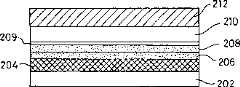
图4是根据本发明的另一个实施例一个有机发光器件的剖面图。衬底202,阳极层204,有机层206,208,与上述第一实施例所述的是一样的。在有机层208表面形成厚度5nm的钙薄层209。该层209较好是通过真空蒸发形成,在薄钙层209上形成厚度为0.5微米的硅层210作为高阻层,在硅层210的顶部形成厚度为0.5微米的铝层212。FIG. 4 is a cross-sectional view of an organic light emitting device according to another embodiment of the present invention. The
使用位于高阻层和发光有机层之间的导体材料(此时为钙)薄层是有利的,因为它有效地起到熔断器一样的作用,如果薄导体层的一部分经受因薄导体层该部分下面的有机层部分内缺陷引起的,异常高电流时,薄导体层的该部分汽化,因此使流过导电缺陷的电流停止和改善器件的性能。也可以在器件制成之后通过一个高电流流经器件的方法来隔离导电缺陷。The use of a thin layer of conductive material (in this case calcium) between the high resistance layer and the light-emitting organic layer is advantageous because it effectively acts like a fuse, if a part of the thin conductive layer is subjected to damage caused by the thin conductive layer. Caused by defects in portions of the underlying organic layer, at abnormally high currents, that portion of the thin conductor layer vaporizes, thereby stopping current flow through the conductive defects and improving device performance. Conductive defects can also be isolated after device fabrication by passing a high current through the device.
尽管在上述实施例中器件有一个高阻的阴极,作为替代,高阻的阳极也可以应用到这种场合,例如采用以下方式生产OLED,首先在玻璃衬底上形成阴极,通过旋涂在阴极上淀积一层发光有机材料,最后在发光有机材料层上形成阳极。对阳极来说,优选高阻电极层包括一种高功函数的材料,或者在高阻电极层和发光有机层之间设有一个高功函数材料薄层。Although the device has a high-resistance cathode in the above embodiments, a high-resistance anode can also be applied to this occasion as an alternative. For example, OLEDs are produced in the following manner. A layer of light-emitting organic material is deposited on it, and finally an anode is formed on the layer of light-emitting organic material. For the anode, it is preferred that the high resistance electrode layer comprises a high work function material, or a thin layer of high work function material is provided between the high resistance electrode layer and the light emitting organic layer.
参考图5,提供用于本发明的第五个方面的发光显示时使用的,根据本发明第六个方面的发光器件,该器件作为一个背后照明使用。它包含玻璃衬底302,淀积玻璃衬底302上的阳极层304,淀积在阳极层304上的有机空穴输运层306,淀积在空穴输运层306上的电致发光聚合物层308,在电致发光聚合物层308上连续的金属阴极层310。图6表示一个淀积在玻璃衬底上的阳极层的部分截面示意图,以展示阳极层304的图形特性,它包含小的子电极320排列成平行的行和列阵列的二维阵列。在空穴输运层306不同部分的下面形成每一个共面的子电极,这些子电极的面积尺寸和它们之间的间距非常小以至于器件产生的光的观察者在正常观察条件下用器件不能察觉到它们。每一个子电极320由一个可熔连接物322连接直接邻近它在同一行和列上的其他子电极,每一个可熔连接物的材料和尺寸是这样来选择的,在正常操作条件下可熔连接物的电压降非常低,但如果经受异常高电流(例如由位于电极和子电极之间有机层中该部分的缺陷所产生)它将过热和断裂,从而从其它背景光中隔离该缺陷位置,最终增强器件的性能。Referring to FIG. 5, there is provided a light-emitting device according to a sixth aspect of the present invention for use in a light-emitting display of the fifth aspect of the present invention, which is used as a backlight. It comprises a
阳极的子电极和可熔连接物也可以例如用ITO制成,子电极和可熔连接物形成的图形阵列可,例如按以下方式形成:首先在玻璃衬底上淀积一连续的ITO层,然后使用例如光刻工艺选择性地蚀刻该连续的层以形成图形阵列。或者,子电极和可熔连接物可以由不同材料制成。The sub-electrode and the fusible link of the anode also can for example be made with ITO, and the pattern array that the sub-electrode and the fusible link form can, for example, be formed in the following manner: first a continuous ITO layer is deposited on the glass substrate, The successive layers are then selectively etched using, for example, a photolithographic process to form a patterned array. Alternatively, the sub-electrodes and the fusible link may be made of different materials.
阴极可以用上面对阳极所述的同一种方法附加地或替代地由用可熔连接物连接的子电极形成。但是,上面所述的这种器件的阴极层是淀积在相对敏感的有机层顶部,通常应注意不要对下面的有机层带来不适当的损伤。由于这个原因,更优选的是通过阴罩板淀积而形成阴极层图形,而不是蚀刻工艺。The cathode may additionally or alternatively be formed from sub-electrodes connected by fusible links in the same manner as described above for the anode. However, in the devices described above, the cathode layer is deposited on top of the relatively sensitive organic layers, and care should generally be taken not to cause undue damage to the underlying organic layers. For this reason, it is more preferable to pattern the cathode layer by shadow mask deposition rather than an etching process.
图7表示根据本发明一个发光器件的另一实施例,在这个实施例中,玻璃衬底402厚度为1.1mm,上面覆盖方块电阻值为15Ohms/sq,厚度为150nm的氧化铟锡(ITO)404。用标准的光刻和蚀刻工艺对该ITO覆层构图形成一个平行的行序列。在ITO/玻璃衬底上通过旋涂形成掺有聚苯乙烯磺酸的聚亚乙二氧基噻吩(PEDT/PSS)层406,并在150℃下烘焙除去水分留下50nm厚的层406。然后在PEDT/PSS层406上通过旋涂淀积发光聚合物层408,该层可以是5%的聚(2,7-(9,9,二正辛基芴)-3,6-(苯并噻二唑)和95%聚(2,7-(9,9-二正辛基芴)(5BTF8)并掺有聚(2,7-(9,9-二正辛基芴-(1,4-亚苯基-((1,4-亚苯基-((4-仲丁基苯基)亚氨基)-1,4-亚苯基))(TFB)的混合物,厚度为75nm。然后在真空室中通过共蒸镀LiF和Al在发光聚合物层408上淀积LiF/Al混合物层410以在发光聚合物层408上形成一个欧姆接触。LiF/Al混合物层410淀积到厚度能充分覆盖在发光聚合物层408的表面上的任何缺陷。在100级洁净室中制备器件时,所述厚度在0.5到1微米之间。然后在LiF/Al层410上淀积铝层412厚度为0.5微米,使用一般的光刻工艺构图,在垂直于ITO平行行序列的方向上形成规则间隔的平行列序列,因此确定彼此空间重叠的ITO平行行和Al平行列序列的规则像素矩阵。Fig. 7 shows another embodiment of a light-emitting device according to the present invention. In this embodiment, the
LiF/Al物理混合物是通过渗透机制导电的各向同性导体,混合物的电阻率由LiF/Al混合物中Al的相对比例来确定。LiF/Al混合物层中LiF和Al的相对比例是根据该层希望的电阻率确定的。希望的电阻率会当然根据该层的所需厚度变化,但是它基本上应使该层电阻不太高不导致驱动电压显著增加(因为它将减小器件的功率效率)但它也高到足以保证将相邻近的列之间的串扰减小到一个很小的级别。因此希望的电阻率取决于几个因素,例如Al列的数量和间距(取决于希望的分辨率),每一列相对相邻近的列顺序驱动的电压,器件工作时的电流密度。The LiF/Al physical mixture is an isotropic conductor that conducts electricity through a percolation mechanism, and the resistivity of the mixture is determined by the relative proportion of Al in the LiF/Al mixture. The relative proportions of LiF and Al in the LiF/Al mixture layer are determined according to the desired resistivity of the layer. The desired resistivity will of course vary depending on the desired thickness of the layer, but it should basically be such that the layer resistance is not too high to cause a significant increase in drive voltage (as it would reduce the power efficiency of the device) but it is high enough Guaranteed to reduce the crosstalk between adjacent columns to a very small level. The desired resistivity therefore depends on several factors, such as the number and spacing of Al columns (depending on the desired resolution), the voltage at which each column is sequentially driven relative to adjacent columns, and the current density at which the device operates.
尽管一个标准的背后发光的LED在相对较低的电流密度下运行:一般1mA/cm2,但点矩阵显示LED工作的电流密度一般会更高,因为,例如在无源的矩阵器件中,这些行是顺序地被驱动,一般该更高的电流密度对应于无脉冲的电流密度(如果作为背后发光器件使用,器件运行时的电流密度)乘以顺序驱动的行数。因此具有100个行的器件工作时一般的电流密度是100mA/cm2。Although a standard backlit LED operates at relatively low current densities: typically 1mA/cm2 , dot-matrix display LEDs operate at generally higher current densities because, for example, in passive matrix devices, these Rows are driven sequentially, and generally this higher current density corresponds to the current density without pulses (if used as a backside emitting device, the current density when the device is operating) multiplied by the number of rows driven sequentially. A device with 100 rows is therefore typically operated at a current density of 100 mA/cm2 .
如果该层的厚度为0.5微米,LiF/Al混合物的电阻率能最高达2×104ohm/cm,不会导致驱动电压增加超过0.1V。如果驱动电压的增加最高为1V是可以接受的,LiF/Al混合物的电阻率可以最高到2×105ohm/cm,如果在器件中所用层厚度为0.5微米和电阻率是2×105ohm/cm,该器件中上面的铝层和ITO阳极层分别构图形成列和行,每一个行和列的节距1mm,间隔0.5mm,长50m,然后,与仅仅是一个像素发光时流经器件的电流250μA相比,被驱动的列的两侧面上相邻近的列的漏电流仅是0.5μA(基于假定被驱动的列电压是10V,被驱动的列的每一个侧面上相邻近的列接地)。If the thickness of this layer is 0.5 micron, the LiF/Al mixture can have a resistivity of up to 2×10⁴ ohm/cm without causing an increase in driving voltage of more than 0.1V. If an increase in drive voltage of up to 1 V is acceptable, the resistivity of LiF/Al mixtures can be up to 2×10⁵ ohm/cm if the layer thickness used in the device is 0.5 μm and the resistivity is 2×10⁵ ohm /cm, the upper aluminum layer and the ITO anode layer in the device are respectively patterned to form columns and rows, the pitch of each row and column is 1mm, the interval is 0.5mm, and the length is 50m, and then, when only one pixel emits light, it flows through the device Compared with the current 250μA of the driven column, the leakage current of the adjacent columns on both sides of the driven column is only 0.5μA (based on the assumption that the driven column voltage is 10V, the adjacent columns on each side of the driven column column ground).
上面所述的实施例也有一个优点,即铝层和发光有机层之间的高阻层包含一种含有低功函数元素的材料,如LiF,这样有助于电子注入到发光聚合物内,因此改善了器件的性能。The embodiment described above also has the advantage that the high resistance layer between the aluminum layer and the light-emitting organic layer comprises a material containing low work function elements, such as LiF, which facilitates electron injection into the light-emitting polymer, thus Improved device performance.
图8表示根据本发明有机发光器件的另一实施例。显示在图8中的器件与图7中的在衬底、阳极和有机层是一样的,相同的数字表示相同的部件。图8中的器件与图7所示器件的不同之处包括阴极结构,该阴极包含一层厚度约为5nm的LiF层414。该层414可以用一般的淀积技术淀积,但是优选用热蒸发技术来淀积,以减小对下面有机层的损伤。在该LiF薄层414的顶部淀积半导体材料层416,例如LiF和Al物理混合物层,其厚度范围从0.5到1微米,下一步,铝层412淀积到LiF/Al混合物层416的顶部达到厚度为0.5微米,形成一个欧姆接触,然后使用一般的构图技术,构图铝层412形成在垂直于阳极行序列方向上延伸的平行列序列。相对较厚的LiF/Al混合物层16可保证下面的有机层在构图工序中被充分保护起来,LiF/Al混合物层416的电阻是这样:它不增加器件的驱动电压到难以承受的程度,同时还防止邻近的阴极列之间的横向漏电流(串扰)。提供邻近发光有机区域的LiF薄层414,增强电子从阴极到发光有机区域的注入。Fig. 8 shows another embodiment of an organic light emitting device according to the present invention. The device shown in FIG. 8 is the same as in FIG. 7 in terms of substrate, anode and organic layers, and like numbers indicate like parts. The device in FIG. 8 differs from the device shown in FIG. 7 in that the cathode structure includes a layer 414 of LiF with a thickness of about 5 nm. This layer 414 can be deposited using conventional deposition techniques, but is preferably deposited using thermal evaporation techniques to minimize damage to the underlying organic layers. Deposit semiconductor material layer 416 on the top of this LiF thin layer 414, for example LiF and Al physical mixture layer, its thickness ranges from 0.5 to 1 micron, next step,
尽管图7和图8显示的实施例表示一个有构图电极的高阻电极层的应用,它也同样可以和构图的阳极一起使用在以下情形,其中OLED用以下方式制备:通过首先在玻璃衬底上形成构图阴极,在阴极上淀积一层或多层有机材料层,最后在有机材料的最上层形成阳极。对阳极来说,邻近发光有机区域的电极层较好包含至少一种有高功函数的元素以增强正电荷载流子(空穴)从阳极注入到发光有机区域内。Although the embodiment shown in Figures 7 and 8 represents the application of a high-resistance electrode layer with patterned electrodes, it can equally be used with patterned anodes in the case where an OLED is fabricated by first forming a layer on a glass substrate A patterned cathode is formed on the cathode, one or more organic material layers are deposited on the cathode, and finally an anode is formed on the uppermost layer of the organic material. For the anode, the electrode layer adjacent to the light emitting organic region preferably contains at least one element with a high work function to enhance the injection of positive charge carriers (holes) from the anode into the light emitting organic region.
Claims (59)
Translated fromChineseApplications Claiming Priority (4)
| Application Number | Priority Date | Filing Date | Title |
|---|---|---|---|
| GBGB9827699.1AGB9827699D0 (en) | 1998-12-16 | 1998-12-16 | Organic light-emitting devices |
| GB9827699.1 | 1998-12-16 | ||
| GBGB9907120.1AGB9907120D0 (en) | 1998-12-16 | 1999-03-26 | Organic light-emissive devices |
| GB9907120.1 | 1999-03-26 |
Related Child Applications (1)
| Application Number | Title | Priority Date | Filing Date |
|---|---|---|---|
| CN02142173.0ADivisionCN1242495C (en) | 1998-12-16 | 1999-12-15 | Organic light-emitting device |
Publications (2)
| Publication Number | Publication Date |
|---|---|
| CN1334967Atrue CN1334967A (en) | 2002-02-06 |
| CN1184703C CN1184703C (en) | 2005-01-12 |
Family
ID=26314844
Family Applications (2)
| Application Number | Title | Priority Date | Filing Date |
|---|---|---|---|
| CNB99815945XAExpired - Fee RelatedCN1184703C (en) | 1998-12-16 | 1999-12-15 | organic light emitting device |
| CN02142173.0AExpired - Fee RelatedCN1242495C (en) | 1998-12-16 | 1999-12-15 | Organic light-emitting device |
Family Applications After (1)
| Application Number | Title | Priority Date | Filing Date |
|---|---|---|---|
| CN02142173.0AExpired - Fee RelatedCN1242495C (en) | 1998-12-16 | 1999-12-15 | Organic light-emitting device |
Country Status (8)
| Country | Link |
|---|---|
| US (2) | US7005196B1 (en) |
| EP (1) | EP1145337A1 (en) |
| JP (2) | JP3662496B2 (en) |
| KR (2) | KR100546876B1 (en) |
| CN (2) | CN1184703C (en) |
| AU (1) | AU1788200A (en) |
| GB (1) | GB9907120D0 (en) |
| WO (1) | WO2000036662A1 (en) |
Cited By (5)
| Publication number | Priority date | Publication date | Assignee | Title |
|---|---|---|---|---|
| CN101606250A (en)* | 2007-02-12 | 2009-12-16 | 皇家飞利浦电子股份有限公司 | Large area light emitting diode light source |
| CN101931059A (en)* | 2010-07-27 | 2010-12-29 | 北京大学 | A kind of double conduction electrode, OLED device and preparation method based on double conduction electrode |
| CN104124397A (en)* | 2013-04-24 | 2014-10-29 | 海洋王照明科技股份有限公司 | Organic electroluminescent device and preparation method thereof |
| CN104124380A (en)* | 2013-04-24 | 2014-10-29 | 海洋王照明科技股份有限公司 | Organic electroluminescent device and preparation method thereof |
| CN104167508A (en)* | 2013-05-17 | 2014-11-26 | 索尼公司 | Light emitting device, method of manufacturing the light emitting device, and display unit |
Families Citing this family (44)
| Publication number | Priority date | Publication date | Assignee | Title |
|---|---|---|---|---|
| US6509581B1 (en)* | 2000-03-29 | 2003-01-21 | Delta Optoelectronics, Inc. | Structure and fabrication process for an improved polymer light emitting diode |
| US6680578B2 (en)* | 2001-09-19 | 2004-01-20 | Osram Opto Semiconductors, Gmbh | Organic light emitting diode light source |
| JP2003163078A (en)* | 2001-11-28 | 2003-06-06 | Hitachi Ltd | Display device |
| JP2006501617A (en)* | 2002-10-01 | 2006-01-12 | コーニンクレッカ フィリップス エレクトロニクス エヌ ヴィ | Electroluminescent display with improved light external coupling |
| JP2004235548A (en)* | 2003-01-31 | 2004-08-19 | Nec Electronics Corp | Semiconductor device and its fabricating method |
| DE102004025578B4 (en)* | 2004-05-25 | 2009-04-23 | Applied Materials Gmbh & Co. Kg | Method for producing organic, light-emitting surface elements and use of this method |
| JP4550529B2 (en)* | 2004-09-02 | 2010-09-22 | 株式会社 日立ディスプレイズ | Liquid crystal display |
| KR101362468B1 (en) | 2004-09-13 | 2014-02-11 | 가부시키가이샤 한도오따이 에네루기 켄큐쇼 | Lighting Device |
| JP4525303B2 (en)* | 2004-11-10 | 2010-08-18 | 富士電機ホールディングス株式会社 | Organic EL device and method for manufacturing the same |
| US7259391B2 (en)* | 2004-12-22 | 2007-08-21 | General Electric Company | Vertical interconnect for organic electronic devices |
| WO2006104020A1 (en)* | 2005-03-25 | 2006-10-05 | Semiconductor Energy Laboratory Co., Ltd. | Light emitting element, light emitting device and electric appliance using the same |
| JP2006324600A (en)* | 2005-05-20 | 2006-11-30 | Toyota Industries Corp | Light emitting device and liquid crystal display device |
| KR100721948B1 (en)* | 2005-08-30 | 2007-05-25 | 삼성에스디아이 주식회사 | Organic electroluminescent display and manufacturing method thereof |
| EP1978576A3 (en)* | 2007-04-03 | 2012-10-17 | Fujikura, Ltd. | Organic light-emitting diode element and optical interconnection module |
| US8167562B2 (en) | 2007-06-29 | 2012-05-01 | Denso Corporation | Centrifugal fan and blower having the same |
| JP2009021073A (en)* | 2007-07-11 | 2009-01-29 | Sumitomo Chemical Co Ltd | Self-luminous element, lighting device and display device |
| DE102007055137A1 (en)* | 2007-11-19 | 2009-05-20 | Fraunhofer-Gesellschaft zur Förderung der angewandten Forschung e.V. | Organic light emitting diode and method for its production |
| JP2010056075A (en) | 2008-07-29 | 2010-03-11 | Sony Corp | Light-emitting element and organic electroluminescent display device |
| JP2010056211A (en)* | 2008-08-27 | 2010-03-11 | Seiko Epson Corp | Organic el device and process of reproducing the same |
| JP5115491B2 (en)* | 2009-02-12 | 2013-01-09 | ソニー株式会社 | Organic electroluminescence device and display device |
| JP2011040244A (en) | 2009-08-10 | 2011-02-24 | Sony Corp | Light-emitting element |
| WO2011052555A1 (en)* | 2009-10-27 | 2011-05-05 | 株式会社アルバック | Organic el lamp |
| JP5423325B2 (en)* | 2009-11-10 | 2014-02-19 | ソニー株式会社 | Light emitting device and manufacturing method thereof |
| JP5463882B2 (en) | 2009-12-01 | 2014-04-09 | ソニー株式会社 | Light emitting device and manufacturing method thereof |
| TWI430442B (en)* | 2010-10-28 | 2014-03-11 | Au Optronics Corp | Organic light emitting device and method of manufacturing same |
| US8552440B2 (en) | 2010-12-24 | 2013-10-08 | Semiconductor Energy Laboratory Co., Ltd. | Lighting device |
| KR101872925B1 (en) | 2010-12-24 | 2018-06-29 | 가부시키가이샤 한도오따이 에네루기 켄큐쇼 | Lighting device |
| CN103262656B (en) | 2010-12-28 | 2016-08-24 | 株式会社半导体能源研究所 | Luminescence unit, light-emitting device and illuminator |
| US9516713B2 (en) | 2011-01-25 | 2016-12-06 | Semiconductor Energy Laboratory Co., Ltd. | Light-emitting device |
| JP5925511B2 (en) | 2011-02-11 | 2016-05-25 | 株式会社半導体エネルギー研究所 | Light emitting unit, light emitting device, lighting device |
| US8735874B2 (en) | 2011-02-14 | 2014-05-27 | Semiconductor Energy Laboratory Co., Ltd. | Light-emitting device, display device, and method for manufacturing the same |
| US8772795B2 (en) | 2011-02-14 | 2014-07-08 | Semiconductor Energy Laboratory Co., Ltd. | Light-emitting device and lighting device |
| WO2013030919A1 (en)* | 2011-08-29 | 2013-03-07 | パイオニア株式会社 | Organic electroluminescence device |
| KR101888157B1 (en)* | 2011-12-20 | 2018-08-14 | 엘지디스플레이 주식회사 | organic light emitting diode display device |
| GB201204670D0 (en) | 2012-03-16 | 2012-05-02 | Cambridge Display Tech Ltd | Optoelectronic device |
| JP2014027192A (en) | 2012-07-30 | 2014-02-06 | Sony Corp | Light-emitting element, display device having the same, and electronic apparatus |
| US9289750B2 (en) | 2013-03-09 | 2016-03-22 | Brigham Young University | Method of making highly porous, stable aluminum oxides doped with silicon |
| KR102109000B1 (en)* | 2017-05-19 | 2020-05-12 | 주성엔지니어링(주) | Organic light emitting device and method for manufacturing the same |
| CN109285962B (en) | 2018-09-25 | 2020-12-01 | 合肥鑫晟光电科技有限公司 | Display substrate, manufacturing method, and display device |
| CN109411627B (en)* | 2018-10-30 | 2020-11-24 | 固安翌光科技有限公司 | Organic light-emitting diode |
| CN109411626B (en)* | 2018-10-30 | 2021-03-02 | 京东方科技集团股份有限公司 | Organic light-emitting device, preparation method thereof, and lighting device |
| CN109698222B (en)* | 2018-12-25 | 2021-03-26 | 固安翌光科技有限公司 | High-stability OLED (organic light emitting diode) illuminating screen body |
| CN113363301B (en)* | 2021-06-02 | 2024-05-17 | 南京昀光科技有限公司 | Silicon-based OLED display panel and preparation method thereof |
| CN114300631B (en)* | 2021-12-29 | 2024-10-29 | 北京维信诺科技有限公司 | Display substrate, display panel and manufacturing method of display substrate |
Family Cites Families (32)
| Publication number | Priority date | Publication date | Assignee | Title |
|---|---|---|---|---|
| US4634934A (en)* | 1982-05-19 | 1987-01-06 | Matsushita Electric Industrial Co. Ltd. | Electroluminescent display device |
| JPS60124397A (en)* | 1983-12-08 | 1985-07-03 | コーア株式会社 | electroluminescent element |
| JPS62285396A (en)* | 1986-06-02 | 1987-12-11 | 松下電器産業株式会社 | Dc driven thin film el device |
| JPS6369193A (en)* | 1986-09-10 | 1988-03-29 | 日本電気株式会社 | El device and manufacture of the same |
| JPS6396896A (en)* | 1986-10-14 | 1988-04-27 | 日立マクセル株式会社 | electroluminescent element |
| JPH01260796A (en)* | 1988-04-12 | 1989-10-18 | Nippon Sheet Glass Co Ltd | Electroluminescent element |
| JPH0249397A (en)* | 1988-08-10 | 1990-02-19 | Nippon Sheet Glass Co Ltd | Electroluminescent element |
| JP3135899B2 (en) | 1989-06-06 | 2001-02-19 | 株式会社リコー | Electrical element |
| JP2818255B2 (en) | 1990-05-08 | 1998-10-30 | 出光興産株式会社 | Method for manufacturing organic electroluminescence device |
| JPH088148B2 (en)* | 1990-12-18 | 1996-01-29 | 富士ゼロックス株式会社 | EL light emitting element |
| JPH04276668A (en)* | 1991-03-04 | 1992-10-01 | Nippon Sheet Glass Co Ltd | Charge injection type electroluminescence element |
| JPH04280095A (en)* | 1991-03-06 | 1992-10-06 | Nippon Sheet Glass Co Ltd | Direct current electroluminescence element |
| US5314207A (en)* | 1992-06-10 | 1994-05-24 | Roadmaster Corporation | Bicycle with simulated motorcycle parts |
| JPH0737687A (en)* | 1993-07-20 | 1995-02-07 | Nippon Sheet Glass Co Ltd | Resistance type ac thin film el element |
| US5482896A (en)* | 1993-11-18 | 1996-01-09 | Eastman Kodak Company | Light emitting device comprising an organic LED array on an ultra thin substrate and process for forming same |
| JP3551475B2 (en)* | 1994-06-25 | 2004-08-04 | 凸版印刷株式会社 | Thin-film EL device |
| JP2931229B2 (en)* | 1995-02-13 | 1999-08-09 | 出光興産株式会社 | Organic electroluminescence device |
| US5858561A (en) | 1995-03-02 | 1999-01-12 | The Ohio State University | Bipolar electroluminescent device |
| US5663573A (en) | 1995-03-17 | 1997-09-02 | The Ohio State University | Bipolar electroluminescent device |
| JP3561549B2 (en)* | 1995-04-07 | 2004-09-02 | 三洋電機株式会社 | Organic electroluminescence device |
| US5798170A (en)* | 1996-02-29 | 1998-08-25 | Uniax Corporation | Long operating life for polymer light-emitting diodes |
| JP3645642B2 (en) | 1996-03-25 | 2005-05-11 | Tdk株式会社 | Organic electroluminescence device |
| DE19616545B4 (en)* | 1996-04-25 | 2006-05-11 | Siemens Ag | Fast radiation detector |
| US5677572A (en)* | 1996-07-29 | 1997-10-14 | Eastman Kodak Company | Bilayer electrode on a n-type semiconductor |
| US5776622A (en) | 1996-07-29 | 1998-07-07 | Eastman Kodak Company | Bilayer eletron-injeting electrode for use in an electroluminescent device |
| US5739545A (en)* | 1997-02-04 | 1998-04-14 | International Business Machines Corporation | Organic light emitting diodes having transparent cathode structures |
| US5920080A (en)* | 1997-06-23 | 1999-07-06 | Fed Corporation | Emissive display using organic light emitting diodes |
| GB9718393D0 (en)* | 1997-08-29 | 1997-11-05 | Cambridge Display Tech Ltd | Electroluminescent Device |
| US6069442A (en)* | 1997-09-18 | 2000-05-30 | Eastman Kodak Company | Organic electroluminescent device with inorganic electron transporting layer |
| JPH11111461A (en)* | 1997-09-30 | 1999-04-23 | Minolta Co Ltd | Organic electroluminescent element |
| JP3078257B2 (en)* | 1998-04-15 | 2000-08-21 | ティーディーケイ株式会社 | Organic EL display device and manufacturing method thereof |
| US6566676B1 (en)* | 1999-09-21 | 2003-05-20 | Fuji Photo Film Co., Ltd. | Image detector |
- 1999
- 1999-03-26GBGBGB9907120.1Apatent/GB9907120D0/ennot_activeCeased
- 1999-12-15JPJP2000588818Apatent/JP3662496B2/ennot_activeExpired - Lifetime
- 1999-12-15EPEP99961189Apatent/EP1145337A1/ennot_activeCeased
- 1999-12-15CNCNB99815945XApatent/CN1184703C/ennot_activeExpired - Fee Related
- 1999-12-15WOPCT/GB1999/004150patent/WO2000036662A1/ennot_activeApplication Discontinuation
- 1999-12-15CNCN02142173.0Apatent/CN1242495C/ennot_activeExpired - Fee Related
- 1999-12-15KRKR1020047014048Apatent/KR100546876B1/ennot_activeExpired - Lifetime
- 1999-12-15USUS09/868,351patent/US7005196B1/ennot_activeExpired - Lifetime
- 1999-12-15AUAU17882/00Apatent/AU1788200A/ennot_activeAbandoned
- 1999-12-15KRKR10-2001-7007617Apatent/KR100461152B1/ennot_activeExpired - Fee Related
- 2005
- 2005-01-13JPJP2005006576Apatent/JP4837286B2/ennot_activeExpired - Fee Related
- 2006
- 2006-01-20USUS11/337,146patent/US7255939B2/ennot_activeExpired - Lifetime
Cited By (6)
| Publication number | Priority date | Publication date | Assignee | Title |
|---|---|---|---|---|
| CN101606250A (en)* | 2007-02-12 | 2009-12-16 | 皇家飞利浦电子股份有限公司 | Large area light emitting diode light source |
| CN101931059A (en)* | 2010-07-27 | 2010-12-29 | 北京大学 | A kind of double conduction electrode, OLED device and preparation method based on double conduction electrode |
| CN101931059B (en)* | 2010-07-27 | 2012-09-05 | 北京大学 | Double electrode, OLED device based on same and manufacturing method |
| CN104124397A (en)* | 2013-04-24 | 2014-10-29 | 海洋王照明科技股份有限公司 | Organic electroluminescent device and preparation method thereof |
| CN104124380A (en)* | 2013-04-24 | 2014-10-29 | 海洋王照明科技股份有限公司 | Organic electroluminescent device and preparation method thereof |
| CN104167508A (en)* | 2013-05-17 | 2014-11-26 | 索尼公司 | Light emitting device, method of manufacturing the light emitting device, and display unit |
Also Published As
| Publication number | Publication date |
|---|---|
| CN1242495C (en) | 2006-02-15 |
| JP2002532848A (en) | 2002-10-02 |
| US7255939B2 (en) | 2007-08-14 |
| KR100546876B1 (en) | 2006-11-23 |
| EP1145337A1 (en) | 2001-10-17 |
| CN1400676A (en) | 2003-03-05 |
| JP4837286B2 (en) | 2011-12-14 |
| GB9907120D0 (en) | 1999-05-19 |
| US20060119253A1 (en) | 2006-06-08 |
| KR20010093847A (en) | 2001-10-29 |
| KR20040099309A (en) | 2004-11-26 |
| JP2005209647A (en) | 2005-08-04 |
| AU1788200A (en) | 2000-07-03 |
| HK1050425A1 (en) | 2003-06-20 |
| WO2000036662A1 (en) | 2000-06-22 |
| US7005196B1 (en) | 2006-02-28 |
| CN1184703C (en) | 2005-01-12 |
| JP3662496B2 (en) | 2005-06-22 |
| KR100461152B1 (en) | 2004-12-13 |
Similar Documents
| Publication | Publication Date | Title |
|---|---|---|
| CN1334967A (en) | Organic light emitting device | |
| US8927976B2 (en) | Organic EL element and production method for same | |
| JP4974978B2 (en) | Method for manufacturing organic electroluminescence device | |
| CN102106186B (en) | Organic EL display panel and method for manufacturing same | |
| CN102893424B (en) | Organic Electroluminescent Devices | |
| EP2375865A1 (en) | Light emission device and method for manufacturing same | |
| JP5543600B2 (en) | LIGHT EMITTING ELEMENT, LIGHT EMITTING DEVICE HAVING LIGHT EMITTING ELEMENT, AND LIGHT EMITTING ELEMENT MANUFACTURING METHOD | |
| US20020117663A1 (en) | Method for producing an organic light emitting device (OLED) and structure produced thereby | |
| CN1573883A (en) | Flat panel display | |
| KR100903101B1 (en) | Organic light emitting display device and manufacturing method thereof | |
| TW201008372A (en) | Light emitting device and manufacturing method of light emitting device | |
| JP4165145B2 (en) | Organic light emitting display | |
| JP6143763B2 (en) | Improved masking for light emitting device patterns | |
| JP6040445B2 (en) | Organic EL panel and manufacturing method thereof | |
| JP5540503B2 (en) | Electronic device manufacturing method and short-circuit body | |
| HK1050425B (en) | Organic light-emitting devices | |
| KR100866886B1 (en) | Manufacturing method of ODL device | |
| US20050040391A1 (en) | Display with dummy edge electrode | |
| KR100341536B1 (en) | Method for producing an organic light emitting device and a concerning device | |
| CN119403360A (en) | A luminous screen | |
| JP2004095456A (en) | Organic electroluminescent display device |
Legal Events
| Date | Code | Title | Description |
|---|---|---|---|
| C06 | Publication | ||
| C10 | Entry into substantive examination | ||
| PB01 | Publication | ||
| SE01 | Entry into force of request for substantive examination | ||
| C14 | Grant of patent or utility model | ||
| GR01 | Patent grant | ||
| CF01 | Termination of patent right due to non-payment of annual fee | Granted publication date:20050112 Termination date:20181215 | |
| CF01 | Termination of patent right due to non-payment of annual fee |