CN1333477A - Touch pad, method for making same, and screen input type indicator using same - Google Patents
Touch pad, method for making same, and screen input type indicator using sameDownload PDFInfo
- Publication number
- CN1333477A CN1333477ACN01125463ACN01125463ACN1333477ACN 1333477 ACN1333477 ACN 1333477ACN 01125463 ACN01125463 ACN 01125463ACN 01125463 ACN01125463 ACN 01125463ACN 1333477 ACN1333477 ACN 1333477A
- Authority
- CN
- China
- Prior art keywords
- substrate
- wiring electrode
- touch panel
- lead
- connection area
- Prior art date
- Legal status (The legal status is an assumption and is not a legal conclusion. Google has not performed a legal analysis and makes no representation as to the accuracy of the status listed.)
- Pending
Links
Images


Classifications
- G—PHYSICS
- G06—COMPUTING OR CALCULATING; COUNTING
- G06F—ELECTRIC DIGITAL DATA PROCESSING
- G06F3/00—Input arrangements for transferring data to be processed into a form capable of being handled by the computer; Output arrangements for transferring data from processing unit to output unit, e.g. interface arrangements
- G06F3/01—Input arrangements or combined input and output arrangements for interaction between user and computer
- G06F3/03—Arrangements for converting the position or the displacement of a member into a coded form
- G06F3/041—Digitisers, e.g. for touch screens or touch pads, characterised by the transducing means
- G06F3/045—Digitisers, e.g. for touch screens or touch pads, characterised by the transducing means using resistive elements, e.g. a single continuous surface or two parallel surfaces put in contact
- G—PHYSICS
- G06—COMPUTING OR CALCULATING; COUNTING
- G06F—ELECTRIC DIGITAL DATA PROCESSING
- G06F3/00—Input arrangements for transferring data to be processed into a form capable of being handled by the computer; Output arrangements for transferring data from processing unit to output unit, e.g. interface arrangements
- G06F3/01—Input arrangements or combined input and output arrangements for interaction between user and computer
- G06F3/03—Arrangements for converting the position or the displacement of a member into a coded form
- G06F3/041—Digitisers, e.g. for touch screens or touch pads, characterised by the transducing means
- H—ELECTRICITY
- H05—ELECTRIC TECHNIQUES NOT OTHERWISE PROVIDED FOR
- H05K—PRINTED CIRCUITS; CASINGS OR CONSTRUCTIONAL DETAILS OF ELECTRIC APPARATUS; MANUFACTURE OF ASSEMBLAGES OF ELECTRICAL COMPONENTS
- H05K1/00—Printed circuits
- H05K1/18—Printed circuits structurally associated with non-printed electric components
- H05K1/189—Printed circuits structurally associated with non-printed electric components characterised by the use of a flexible or folded printed circuit
- G—PHYSICS
- G06—COMPUTING OR CALCULATING; COUNTING
- G06F—ELECTRIC DIGITAL DATA PROCESSING
- G06F2203/00—Indexing scheme relating to G06F3/00 - G06F3/048
- G06F2203/041—Indexing scheme relating to G06F3/041 - G06F3/045
- G06F2203/04103—Manufacturing, i.e. details related to manufacturing processes specially suited for touch sensitive devices
- H—ELECTRICITY
- H05—ELECTRIC TECHNIQUES NOT OTHERWISE PROVIDED FOR
- H05K—PRINTED CIRCUITS; CASINGS OR CONSTRUCTIONAL DETAILS OF ELECTRIC APPARATUS; MANUFACTURE OF ASSEMBLAGES OF ELECTRICAL COMPONENTS
- H05K2201/00—Indexing scheme relating to printed circuits covered by H05K1/00
- H05K2201/10—Details of components or other objects attached to or integrated in a printed circuit board
- H05K2201/10007—Types of components
- H05K2201/10128—Display
Landscapes
- Engineering & Computer Science (AREA)
- General Engineering & Computer Science (AREA)
- Theoretical Computer Science (AREA)
- Human Computer Interaction (AREA)
- Physics & Mathematics (AREA)
- General Physics & Mathematics (AREA)
- Microelectronics & Electronic Packaging (AREA)
- Position Input By Displaying (AREA)
- Manufacture Of Switches (AREA)
- Switches That Are Operated By Magnetic Or Electric Fields (AREA)
- Push-Button Switches (AREA)
- Liquid Crystal (AREA)
Abstract
Translated fromChinese
Description
Translated fromChinese技术领域technical field
本发明涉及一种触摸板,该触摸板通过由按压或按压操作引起的电阻变化来探测相应的输入坐标;以及一种制造该触摸板的方法;还涉及由层迭该种触摸板所组成的屏幕输入型显示装置。The present invention relates to a touch panel which detects corresponding input coordinates through a change in resistance caused by pressing or pressing operation; and a method of manufacturing the touch panel; Screen input type display device.
背景技术Background technique
触摸板是一种用来通过手指或笔尖的按压输入字符/数字或图像的装置。此外,触摸板是层迭在显示装置的显示表面上,如平板显示器或阴极射线管显示器(CRT)上,来作为选择显示表面上的显示信息或输入字符/数字或图像的装置。A touchpad is a device used to input characters/numbers or images by pressing with a finger or a pen tip. In addition, a touch panel is laminated on a display surface of a display device, such as a flat panel display or a cathode ray tube display (CRT), as a means for selecting information displayed on the display surface or inputting characters/numbers or images.
用来作为个人电脑、便携式信息终端或其它信息装置监视器的显示装置。有众所周知的使用液晶板、有机EL板或等离子体板等的平板型显示装置,或使用阴极射线管的显示装置。A display device used as a monitor for personal computers, portable information terminals, or other information devices. There are well-known flat-panel display devices using a liquid crystal panel, an organic EL panel, or a plasma panel, or a display device using a cathode ray tube.
虽然在当前情况下触摸板也可用来作为独立的信息输入装置,但它通常以层迭在显示装置的显示表面上的方式使用。Although a touch panel is also used as an independent information input device in the present situation, it is generally used in a manner laminated on a display surface of a display device.
在使用液晶板的显示装置中,用照明光照射产生在液晶板上的图像。经过透射或反射后,照明光从液晶板发射到显示表面上。这样,图象就可见了。另一方面,有机EL板对有机电致发光材料薄膜施加一电场,这样通过控制电流就可以实现显示。等离子体板通过等离子体放电产生的紫外线激发荧光物质来实现显示。In a display device using a liquid crystal panel, an image generated on the liquid crystal panel is irradiated with illumination light. After transmission or reflection, the illuminating light is emitted from the liquid crystal panel onto the display surface. Thus, the image becomes visible. On the other hand, the organic EL panel applies an electric field to the thin film of organic electroluminescent material, so that display can be realized by controlling the current. The plasma panel realizes display by exciting fluorescent substances through ultraviolet rays generated by plasma discharge.
通常,在目前情况下,液晶显示装置一般用来作为平板显示装置。在一个液晶显示装置中,液晶板的使用方式如下。也就是说,在液晶板中,一液晶层放在一对基片的缝隙中,这对基片是互相面对面平行排列的,它们具有像素选择电极等。这样,在选定像素的部分,液晶分子的序列状态变化产生了图像。实际上产生的图像是不可见的。因此,液晶板要用外部给定的光线照射。这样,通过透射或反射外部光的光线就可看到图像。Generally, in the present situation, a liquid crystal display device is generally used as a flat panel display device. In a liquid crystal display device, the liquid crystal panel is used as follows. That is, in a liquid crystal panel, a liquid crystal layer is placed in a gap between a pair of substrates, which are arranged in parallel facing each other, and which have pixel selection electrodes and the like. In this way, at selected pixel portions, sequential state changes of the liquid crystal molecules produce an image. The resulting image is actually invisible. Therefore, the liquid crystal panel is irradiated with a given light from the outside. In this way, an image can be seen by transmitting or reflecting rays of external light.
考虑到它们的作用原理,有各种各样的触摸板。其中,一种所谓的模拟电阻膜型触摸板是最流行的,它通过电阻变化量来探测输入坐标。There are all kinds of touchpads given how they work. Among them, a so-called analog resistive film type touch panel is most popular, which detects input coordinates by the amount of resistance change.
在这种模拟电阻膜型触摸板中,在信息输入面的基片是由一透明的软膜如塑料片制成的;另一基片是由一透明的硬质基材制成的,这种基材最好是玻璃或透明硬塑料。电阻膜分别装在这对透明基片相对的表面上。两维坐标值是输出终端和相应电阻膜之间的电阻值测定的,其中,通过在信息输入端基片上的按压操作使基片上的相应电阻膜相互接触。In this analog resistive film type touch panel, the substrate at the information input surface is made of a transparent soft film such as a plastic sheet; the other substrate is made of a transparent hard substrate, which The substrate is preferably glass or transparent hard plastic. Resistive films are provided on the opposite surfaces of the pair of transparent substrates, respectively. The two-dimensional coordinate value is determined by the resistance value between the output terminal and the corresponding resistance film, wherein the corresponding resistance films on the substrate are brought into contact with each other by pressing operation on the information input terminal substrate.
如上所述,通常在触摸板中这样设定,信息输入是通过使用一种输入操作工具如笔尖来完成的。在这对基片的内表面形成的电阻膜通常是互相电绝缘的。因此,在这对基片之间插入垫片以保证一定的间距,以使基片的电阻膜能够在操作工具笔尖一类的按压下能互相接触。As described above, it is generally set in the touch panel that information input is performed by using an input operation tool such as a pen point. The resistive films formed on the inner surfaces of the pair of substrates are usually electrically insulated from each other. Therefore, a spacer is interposed between the pair of substrates to ensure a certain distance so that the resistive films of the substrates can be brought into contact with each other by pressing such as a pen tip of an operating tool.
但是如果这对基片之间的间距太大,那么通过操作工具的按压产生的软膜也就是信息输入面的基片(上基片)的凹陷量太大以致于产生一种与正常书写不匹配的感觉。这样,就不能产生舒适的输入感觉。But if the spacing between the pair of substrates is too large, the soft film produced by the pressing of the operating tool is that the amount of depression of the substrate (upper substrate) on the information input surface is too large to produce a kind of writing that is different from normal writing. The feeling of matching. Thus, a comfortable input feeling cannot be produced.
另外,当在输入区域端进行输入操作时,软膜的弯曲变化量变大。虽然发生的机率很小,但是在软膜内表面形成的电阻膜(上电阻膜)或者软膜本身可能由于重复的输入操作而破裂。In addition, when an input operation is performed on the input area side, the amount of change in curvature of the soft membrane becomes larger. Although the probability of occurrence is small, the resistance film (upper resistance film) formed on the inner surface of the soft film or the soft film itself may be broken due to repeated input operations.
顺便提及,这样一种屏幕输入型液晶显示装置的一般相关技术的参考文献例子包括JP-A-60-207924和JP-A-3-156818。另一方面,与一对基片的距离相关的参考文献例子包括JP-A-8-94995,JP-A-10-69354,JP-A-8-101740,JP-U-62-81141等。Incidentally, reference examples of general related art of such a screen input type liquid crystal display device include JP-A-60-207924 and JP-A-3-156818. On the other hand, examples of references related to the distance between a pair of substrates include JP-A-8-94995, JP-A-10-69354, JP-A-8-101740, JP-U-62-81141 and the like.
此外,揭示生产触摸板的相关方法的文献的例子有JP-A-6-324784和JP-A-6-324785。Furthermore, examples of documents disclosing related methods of producing touch panels are JP-A-6-324784 and JP-A-6-324785.
在一常规的组成屏幕输入型显示装置的触摸板中如此配置:一上电阻膜和一下电阻膜成形在一对基片各自的内表面的输入区(也就是说,上基片通常是一柔韧性薄膜,而下基片通常是玻璃硬板等)。分别连接到电阻膜的上布线电极和下布线电极分别成形在该对基片的输入区的外围。In a conventional touch panel constituting a screen input type display device, it is configured as follows: an upper resistive film and a lower resistive film are formed in the input area of the respective inner surfaces of a pair of substrates (that is, the upper substrate is usually a flexible permanent film, and the lower substrate is usually a hard glass plate, etc.). Upper wiring electrodes and lower wiring electrodes respectively connected to the resistance films are respectively formed on the peripheries of the input regions of the pair of substrates.
一从该下布线电极伸出的下布线电极引线,一电连接到该上布线电极的基片互联电极,和一从该基片互联电极伸出的上布线电极引线成形在该下基片的输入区的外围部分上。下布线电极引线和上布线电极引线的末段集中在某一地方并延至一引线连接区,该引线连接区装在输入区的外围末段。A lower wiring electrode lead extending from the lower wiring electrode, a substrate interconnect electrode electrically connected to the upper wiring electrode, and an upper wiring electrode lead extending from the substrate interconnect electrode are formed on the lower substrate. on the peripheral portion of the input area. The ends of the leads of the lower wiring electrodes and the leads of the upper wiring electrodes are concentrated at a certain place and extended to a lead connecting area provided at the outer peripheral ends of the input area.
在此引线连接区,通过例如热压接合等方法连接一个有引线的输出印制线路板,它用于从上布线电极引线和下布线电极引线提取输出信号。也就是说,在这种类型的触摸板上,印制线路板所有的端头都装在下基片侧。In this lead connection area, an output printed wiring board with leads for extracting output signals from upper wiring electrode leads and lower wiring electrode leads is connected by a method such as thermocompression bonding. That is, on this type of touch panel, all terminals of the printed wiring board are mounted on the lower substrate side.
通常,这样一个输出印制线路板通过下面方式连接。也就是说,该输出印制线路板被固定于上下基片之间的引线连接区。换句话说,如JP-A-3-156818中所示的,下基片比上基片延伸的长,并且上布线电极引线和下布线电极引线成形在下基片的延伸部分,并从上布线电极和基片互联连电极伸出。然后输出印刷线路板通过热压接合连接。Usually, such an output printed wiring board is connected in the following manner. That is, the output printed wiring board is fixed to the lead connection area between the upper and lower substrates. In other words, as shown in JP-A-3-156818, the lower substrate extends longer than the upper substrate, and upper wiring electrode leads and lower wiring electrode leads are formed on the extended portion of the lower substrate, and are wired from the upper substrate. The electrodes are interconnected with the substrate and the electrodes protrude. The output printed wiring boards are then connected by thermocompression bonding.
在输出印制线路板被固定在上下基片之间的方法中,上基片可以在引线连接区鼓起。因此,要求有工艺能防止由这样的鼓胀所引起的显示变形或输入错误。In the method in which the output printed wiring board is fixed between the upper and lower substrates, the upper substrate may bulge in the lead connection area. Therefore, a process is required to prevent display deformation or input errors caused by such swelling.
另一方面,在JP-A-3-156818揭示的方法中,触摸板的尺寸通过下基片的延伸部分增大。这是防碍实现狭小框架的触摸板的因素之一(显示装置使用该触摸板)。因此,这是一个待解决的问题。On the other hand, in the method disclosed in JP-A-3-156818, the size of the touch panel is increased by the extension of the lower substrate. This is one of the factors preventing realization of a narrow-frame touch panel (which is used by a display device). Therefore, this is an open problem.
为了制造这样的一触摸板,上基片被切成一预定大小和一预定形状,并且其后被调整到与下基片对齐。然后,下基片被分割成单位面板。在这样的制造方法中,上基片必须精确地定位,使其可以通过面板定位调整与下基片对齐。因此,工作效率不能被认为是优秀的。In order to manufacture such a touch panel, the upper substrate is cut into a predetermined size and a predetermined shape, and thereafter adjusted to align with the lower substrate. Then, the lower substrate is divided into unit panels. In such a manufacturing method, the upper substrate must be precisely positioned so that it can be aligned with the lower substrate through panel alignment adjustments. Therefore, work efficiency cannot be considered excellent.
还存在另一个问题,即在切割硬板时产生的异物会污染触摸板。There is another problem that foreign matter generated when cutting the hard board contaminates the touchpad.
此外,上下布线电极引线分别从上下布线电极引出,并置于被上基片覆盖的区域。然后,上下布线电极输出端被集中在引线连接区,并且弯向该引出线连接区。结果,易于在上下布线电极输出端与输出印刷线路板连接的部分附近出现一缺口。异物易于通过这个缺口进入上下基片之间。这样,由于异物的进入,电阻薄膜的性质可能变化。这是引起触摸板故障的因素之一,因此这也是一个待解决的问题。In addition, upper and lower wiring electrode leads are led out from the upper and lower wiring electrodes respectively, and placed in the area covered by the upper substrate. Then, the output terminals of the upper and lower wiring electrodes are concentrated in the lead connection area, and bent toward the lead connection area. As a result, a notch tends to occur near the portion where the output terminals of the upper and lower wiring electrodes are connected to the output printed wiring board. Foreign matter easily enters between the upper and lower substrates through this gap. Thus, the properties of the resistive film may change due to entry of foreign matter. This is one of the factors that cause touchpad failure, so it is also a problem to be solved.
顺便说一下,在JP-A-6-324784和JP A-6324785中揭示的触摸板中,两者的上下基片都是软的基片。在这二个申请中,没有提到在该结构中存在上述的问题,在该结构中上面的软的基片受定位调整与下面的硬的基片面对齐。本发明是针对这种结构的。Incidentally, in the touch panels disclosed in JP-A-6-324784 and JP A-6324785, the upper and lower substrates of both are soft substrates. In both applications, there is no mention of the aforementioned problems in structures in which the upper soft substrate is aligned with the lower hard substrate face by alignment. The present invention is directed to this structure.
本发明的第一个目的是提供一制造触摸板的方法,该方法具有出众的生产效率并且可以防止在切割的时候被异物污染。这样,可以以低成本制造触摸板。A first object of the present invention is to provide a method of manufacturing a touch panel which is superior in production efficiency and which can prevent contamination by foreign matter at the time of cutting. In this way, the touch panel can be manufactured at low cost.
本发明的第二个目的是提供一种触摸板,该触摸板没有故障,具有狭小的框架,并且大小、重量和厚度都降低了。A second object of the present invention is to provide a touch panel that is free from failure, has a narrow frame, and is reduced in size, weight, and thickness.
本发明的第三个目的是提供一种高可靠性的屏幕输入型显示装置,该屏幕输入型显示装置使用一种没有故障,具有狭小型框架,并且大小、重量和厚度都降低了的触摸板。A third object of the present invention is to provide a highly reliable screen input type display device using a touch panel that is free from failure, has a small frame, and is reduced in size, weight and thickness .
发明内容Contents of the invention
为达到第一个目的,根据本发明制造触摸板的一个方法具有下列特征:To achieve the first object, a method of manufacturing a touch panel according to the present invention has the following characteristics:
(1)制造触摸板的方法,包括如下步骤:把上基片和下基片粘接到一起,上基片是由有上电阻膜的软膜制成的,下基片是由具有下电阻膜的硬板制成的;然后,切割上基片和下基片。(1) The method for manufacturing touch panel comprises the steps of: bonding the upper substrate and the lower substrate together, the upper substrate is made of a soft film with an upper resistance film, and the lower substrate is made of a soft film with a lower resistance film. The film is made of a rigid plate; then, the upper and lower substrates are cut.
(2)在上面段落(1)中,下基片是用玻璃或塑料片做的。(2) In the above paragraph (1), the lower substrate is made of glass or plastic sheet.
(3)在上面段落(1)或(2)中,下基片是在切割上基片后才切割的。(3) In the above paragraph (1) or (2), the lower substrate is cut after cutting the upper substrate.
(4)在上面段落(3)中,在上基片用第一刀片切割后,用第二刀片替换第一刀片,然后,切割下基片。(4) In the above paragraph (3), after the upper substrate is cut with the first blade, the first blade is replaced with the second blade, and then, the lower substrate is cut.
(5)在上面段落(1)或(2)中,上基片和下基片同时切割。(5) In the above paragraph (1) or (2), the upper substrate and the lower substrate are cut simultaneously.
(6)在上面段落(1)至(5)的任一段中,下基片是从上基片侧切割。(6) In any of the above paragraphs (1) to (5), the lower substrate is cut from the upper substrate side.
(7)在上面段落(1)至(5)的任一段中,下基片是从上基片的对立侧切割。(7) In any of the above paragraphs (1) to (5), the lower substrate is cut from the opposite side of the upper substrate.
(8)在上面段落(1)至(7)的任一段中,用于切割成许多上基片的第一基材和用于切割成许多下基片的第二基材先粘接到一起,然后切割。(8) In any of the above paragraphs (1) to (7), the first substrate for cutting into many upper substrates and the second substrate for cutting into many lower substrates are first bonded together , and then cut.
(9)在上面(1)至(8)的任一段中,触摸板具有上基片,下基片和用于获取输出信号的输出印刷线路板;下基片具有下布线电极引线和上布线电极引线,下布线电极引线与下电阻膜电连接并延伸到输入区外围末端的引线连接区,上布线电极引线与上电阻膜电连接并延伸到输入区外围末端的引线连接区,下布线电极引线和上布线电极引线在引线连接区与输出印刷线路板相连;并且至少去掉上基片与引线连接区相对应的上基片的一部分。(9) In any of the above (1) to (8), the touch panel has an upper substrate, a lower substrate and an output printed circuit board for obtaining output signals; the lower substrate has lower wiring electrode leads and an upper wiring Electrode leads, lower wiring electrode leads are electrically connected to the lower resistance film and extend to the lead connection area at the peripheral end of the input area, upper wiring electrode leads are electrically connected to the upper resistance film and extend to the lead connection area at the outer end of the input area, the lower wiring electrode Leads and upper wiring electrode leads are connected to the output printed wiring board at the lead connection area; and at least a part of the upper substrate corresponding to the lead connection area is removed.
(10)在上面段落(9)中,在上基片和下基片粘接在一起前,上基片至少去掉与引线连接区相对应的上基片的一部分。(10) In the above paragraph (9), before the upper substrate and the lower substrate are bonded together, the upper substrate has at least a part of the upper substrate corresponding to the lead connection area removed.
(11)在上面段落(9)中,在上基片和下基片粘接在一起后,上基片至少去掉与引线连接区相对应的上基片部分。(11) In the above paragraph (9), after the upper substrate and the lower substrate are bonded together, the upper substrate is removed from at least the portion of the upper substrate corresponding to the lead connection area.
(12)在上面段落(9)中,在切割上基片和下基片前,上基片和下基片被连接到输出印刷线路板。(12) In the above paragraph (9), before cutting the upper substrate and the lower substrate, the upper substrate and the lower substrate are connected to the output printed wiring board.
(13)在上面段落(9)中,在切割上基片和下基片后,上基片和下基片被连接到输出印刷线路板。(13) In the above paragraph (9), after cutting the upper substrate and the lower substrate, the upper substrate and the lower substrate are connected to the output printed wiring board.
(14)在上面(9)至(13)的任一段中,2至20μm高的垫片通过印刷方法成形于下基片的下电阻膜上。(14) In any of the above (9) to (13), a spacer having a height of 2 to 20 µm is formed on the lower resistive film of the lower substrate by a printing method.
根据在(1)至(14)任一段中描述的上述制造方法可以获得以下效果,即上下基片在粘接到一起后切割,这样可以防止异物在切割时进入上下基片间,特别是切割硬板时。更具体的说,可以防止在切割一个玻璃板的下基片时产生的玻璃屑进入上下基片间。另外,在进行印刷时,电阻膜、电极和粘性材料的印刷步骤和清洗步骤可同时进行。因此,提高了工作效率。According to the above-mentioned manufacturing method described in any paragraph (1) to (14), the following effects can be obtained, that is, the upper and lower substrates are bonded together and then cut, which can prevent foreign matter from entering between the upper and lower substrates during cutting, especially when cutting When hard board. More specifically, it is possible to prevent glass shavings generated when cutting the lower substrate of a glass plate from entering between the upper and lower substrates. In addition, when printing is performed, the printing step and cleaning step of the resistive film, electrodes, and adhesive material can be performed simultaneously. Therefore, work efficiency is improved.
上下基片可以同时切割,而不必反转互相面平行的基片。例如通过用激光束或通过用分别为上下基片安装的切刀。如果从上基片侧切割下基片,这对基片可以被同样切割而不需反转。The upper and lower substrates can be cut simultaneously without inverting the substrates whose faces are parallel to each other. For example by using a laser beam or by using cutters provided for the upper and lower substrates respectively. If the lower substrate is cut from the upper substrate side, the pair of substrates can be similarly cut without inversion.
当从与上基片相对的一侧切割下基片时,用于切割下基片的刀片不受上基片的影响。这样,可以在与切割上基片位置相同或相近的位置切割下基片。When cutting the lower substrate from the side opposite to the upper substrate, the blade for cutting the lower substrate is not affected by the upper substrate. In this way, the lower substrate can be cut at the same or close position to that of the upper substrate.
此外,为达到前述的第二个目的,根据本发明的触摸板具有下列特点:In addition, in order to achieve the aforementioned second purpose, the touch panel according to the present invention has the following characteristics:
(15)触摸板包括:具有上电阻膜的上基片、具有下电阻膜的下基片、用于获取输出信号的输出印刷线路板。而其中的下基片,具有下布线电极引线和上布线电极引线,下布线电极引线电连接下电阻膜并延伸到输入区外围末端的引线连接区,上布线电极引线电连接上电阻膜并延伸到输入区外围末端的引线连接区;下布线电极引线和上布线电极引线在引线连接区与输出印刷线路板相连;其中,将上基片与引线连接区相对应的部分去掉使之与输出印刷线路板安装部分的形状一样。(15) The touch panel includes: an upper substrate with an upper resistive film, a lower substrate with a lower resistive film, and an output printed wiring board for acquiring output signals. Wherein the lower substrate has a lower wiring electrode lead and an upper wiring electrode lead, the lower wiring electrode lead is electrically connected to the lower resistance film and extends to the lead connection area at the peripheral end of the input area, and the upper wiring electrode lead is electrically connected to the upper resistance film and extends To the lead connection area at the peripheral end of the input area; the lower wiring electrode lead and the upper wiring electrode lead are connected to the output printed circuit board in the lead connection area; wherein, the part of the upper substrate corresponding to the lead connection area is removed to make it compatible with the output printed circuit board. The shape of the circuit board mounting part is the same.
(16)触摸板包括:具有上电阻膜的上基片、具有下电阻膜的下基片、用于获取输出信号的输出印刷线路板;其中,下基片,具有下布线电极引线和上布线电极引线,下布线电极引线与下电阻膜电连接并延伸到输入区外围末端的引线连接区,上布线电极引线与上电阻膜电连接并延伸到输入区外围末端的引线连接区;其中,下布线电极引线和上布线电极引线在引线连接区与输出印刷线路板相连;其中,下布线电极引线和上布线电极引线的部分或全部被引入输出印刷线路板的沿下基片有引线连接区的一侧的侧表面上;其中,上基片的至少一部分与引线连接区相对应的一侧被全部去掉。(16) The touch panel includes: an upper substrate with an upper resistive film, a lower substrate with a lower resistive film, and an output printed circuit board for obtaining output signals; wherein, the lower substrate has a lower wiring electrode lead and an upper wiring Electrode leads, the lower wiring electrode leads are electrically connected to the lower resistance film and extend to the lead connection area at the peripheral end of the input area, and the upper wiring electrode leads are electrically connected to the upper resistance film and extend to the lead connection area at the outer peripheral end of the input area; wherein, the lower The wiring electrode lead and the upper wiring electrode lead are connected to the output printed circuit board at the lead connection area; wherein, part or all of the lower wiring electrode lead and the upper wiring electrode lead are introduced into the output printed circuit board where there is a lead connection area along the lower substrate On the side surface of one side; wherein, at least a part of the upper substrate is completely removed on the side corresponding to the lead connection area.
按照上面提到的构造,提供一个无故障,具有狭小框架,且尺寸,重量和厚度都减小的触摸板是可能的。According to the above-mentioned construction, it is possible to provide a trouble-free touch panel having a narrow frame and being reduced in size, weight and thickness.
进一步,为达到本发明的第三个目的,根据本发明的屏幕输入型显示装置具有如下特点。Further, in order to achieve the third object of the present invention, the screen input type display device according to the present invention has the following features.
(17)在屏幕输入型显示装置中,触摸板装在显示装置的显示表面上。其中触摸板有:具有上电阻膜的上基片、具有下电阻膜的下基片、用于获取输出信号的输出印刷线路板;下基片具有下布线电极引线和上布线电极引线,下布线电极引线与下电阻膜电连接并延伸到输入区外围末端的引线连接区,上布线电极引线与上电阻膜电连接并延伸到输入区外围末端的引线连接区,下布线电极引线和上布线电极引线在引线连接区与输出印刷线路板相连;将上基片与引线连接区相对应的部分去掉使之与输出印刷线路板安装部分的形状一样。(17) In the screen input type display device, a touch panel is mounted on the display surface of the display device. Wherein the touch panel includes: an upper substrate with an upper resistive film, a lower substrate with a lower resistive film, an output printed circuit board for obtaining output signals; the lower substrate has a lower wiring electrode lead and an upper wiring electrode lead, and the lower wiring The electrode leads are electrically connected to the lower resistance film and extend to the lead connection area at the peripheral end of the input area, the upper wiring electrode leads are electrically connected to the upper resistance film and extend to the lead connection area at the outer end of the input area, the lower wiring electrode leads and the upper wiring electrode The leads are connected to the output printed circuit board in the lead connection area; the part of the upper substrate corresponding to the lead connection area is removed to make it the same shape as the output printed circuit board installation part.
(18)在上面段落(17)中说明的触摸板,至少下基片的下布线电极引线和上布线电极引线的一部分被引入输出印刷线路板的沿下基片有引线连接区一侧的侧表面上。(18) In the touch panel described in the above paragraph (17), at least a part of the lower wiring electrode lead and the upper wiring electrode lead of the lower substrate is introduced into the side of the output printed wiring board along the side where the lower substrate has the lead connection area. On the surface.
(19)在上面段落(17)或(18)中说明的触摸板,上基片的端面位于与下基片的端面相对应的位置。(19) In the touch panel described in the above paragraph (17) or (18), the end face of the upper substrate is located at a position corresponding to the end face of the lower substrate.
(20)在上面的(17)至(19)的任一段中,上基片和下基片通过2至20μm高的垫片相对。(20) In any one of (17) to (19) above, the upper substrate and the lower substrate are opposed via a spacer having a height of 2 to 20 µm.
(21)在屏幕输入型显示装置中,触摸板装在显示装置的显示表面上。其中触摸板有:具有上电阻膜的上基片、具有下电阻膜的下基片、用于获取输出信号的输出印刷线路板;下基片,具有下布线电极引线和上布线电极引线,下布线电极引线与下电阻膜电连接并延伸到输入区外围末端的引线连接区,上布线电极引线与上电阻膜电连接并延伸到输入区外围末端的引线连接区,下布线电极引线和上布线电极引线在引线连接区与输出印刷线路板相连;下布线电极引线和上布线电极引线的部分或全部被引入输出印刷线路板的沿下基片有引线连接区一侧的侧表面上;上基片的至少一部分与引线连接区相对应的一侧被全部去掉。(21) In the screen input type display device, a touch panel is mounted on the display surface of the display device. The touch panel includes: an upper substrate with an upper resistive film, a lower substrate with a lower resistive film, and an output printed circuit board for obtaining output signals; the lower substrate has a lower wiring electrode lead and an upper wiring electrode lead, and a lower wiring electrode lead. The wiring electrode leads are electrically connected to the lower resistance film and extend to the lead connection area at the peripheral end of the input area, the upper wiring electrode leads are electrically connected to the upper resistance film and extend to the lead connection area at the outer peripheral end of the input area, the lower wiring electrode leads and the upper wiring The electrode leads are connected to the output printed circuit board at the lead connection area; part or all of the lower wiring electrode leads and the upper wiring electrode leads are introduced into the side surface of the output printed circuit board along the side of the lower substrate with the lead connection area; the upper substrate At least a portion of the sheet is completely removed on one side corresponding to the lead connection area.
(22)在上面段落(21)中,上基片和下基片通过2至20μm高的垫片相对。(22) In the above paragraph (21), the upper substrate and the lower substrate are opposed via a spacer having a height of 2 to 20 µm.
按照上面提到的构造,提供一种使用触摸板的高可靠性屏幕输入型显示装置是可能的,该触摸板没有故障,具有狭小框架,且尺寸,重量和厚度都减小的触摸板。According to the above-mentioned construction, it is possible to provide a high-reliability screen input type display device using a touch panel that is free from failure, has a narrow frame, and is reduced in size, weight and thickness.
顺便提及,在本发明中当液晶显示装置作显示装置使用时,其液晶板可以是所谓的无源基质型,所谓的有源基质型,或其它任意已知的类型。此外,这样的液晶板可以与反射型的、透射的或半透射/反射型的结合使用。Incidentally, when a liquid crystal display device is used as a display device in the present invention, its liquid crystal panel may be of a so-called passive matrix type, a so-called active matrix type, or any other known type. In addition, such a liquid crystal panel may be used in combination with reflective, transmissive, or transflective/reflective.
此外,如前面所描述的,有机EL板,等离子体板或阴极射线管都可用做显示装置。In addition, as described above, an organic EL panel, a plasma panel or a cathode ray tube can be used as the display device.
而且,本发明不限于上述结构或下面将要说明的实施例的结构。本发明也可应用于所谓的数字型触摸板,其中,按压坐标根据上下基片间的电容变化或电的其它性质的变化测定。基于本发明的技术思想,可以做各种改进。Also, the present invention is not limited to the above structure or the structure of the embodiment to be described below. The invention is also applicable to so-called digital type touch panels, in which the pressing coordinates are determined from changes in capacitance or other properties of electricity between the upper and lower substrates. Based on the technical idea of the present invention, various improvements can be made.
基片粘接在一起后再切割的制造方法也可应用于这样一种触摸板,其中基片互联电极不装在下基片上,而是上布线电极引线在上基片上形成,这样上下基片分别与外部相连,而不互相电连接。The manufacturing method in which the substrates are bonded together and then cut can also be applied to a touch panel in which the substrate interconnection electrodes are not mounted on the lower substrate, but the upper wiring electrode leads are formed on the upper substrate, so that the upper and lower substrates are respectively connected to the outside, but not electrically connected to each other.
附图说明Description of drawings
图1是一典型的剖面图,说明了一个装有根据本发明的触摸板的屏幕输入型显示装置的例子。FIG. 1 is a typical sectional view illustrating an example of a screen input type display device equipped with a touch panel according to the present invention.
图2是一分解透视图,解释了根据本发明的装在屏幕输入型显示装置中的触摸板的第一个实施例的示意结构。FIG. 2 is an exploded perspective view explaining a schematic structure of a first embodiment of a touch panel incorporated in a screen input type display device according to the present invention.
图3是一个主体部分平面图,它一般用来解释图2中所解释的触摸板的引线连接区结构的一个例子;其中,下基片从上基片侧观察。Fig. 3 is a main part plan view which is generally used to explain an example of the structure of the lead connection area of the touch panel explained in Fig. 2; wherein the lower substrate is viewed from the upper substrate side.
图4是沿图3中A-A线的音面图。Fig. 4 is a sound surface diagram along line A-A in Fig. 3 .
图5是沿图3中B-B线的剖面图。Fig. 5 is a sectional view along line B-B in Fig. 3 .
图6是一个典型的平面图,它用来说明按照本发明装在屏幕输入型显示装置上的触摸板的框架狭窄效应。FIG. 6 is a typical plan view illustrating the frame narrowing effect of a touch panel mounted on a screen input type display device according to the present invention.
图7是一个示意图,它用来解释按照本发明装在屏幕输入型显示装置上的触摸板的第二个实施例的示意结构,(a)透视图,(b)侧视图。Fig. 7 is a diagram for explaining a schematic structure of a second embodiment of a touch panel mounted on a screen input type display device according to the present invention, (a) perspective view, (b) side view.
图8是一个示意图,它用来解释按照本发明装在屏幕输入型显示装置上的触摸板的第三个实施例的示意结构。Fig. 8 is a diagram for explaining the schematic structure of a third embodiment of a touch panel mounted on a screen input type display device according to the present invention.
图9是一个示意图,它用来解释按照本发明装在屏幕输入型显示装置上的触摸板的第四个实施例的示意结构,(a)是剖面图,(b)是图9(a)侧视图中D部分的放大视图。Fig. 9 is a schematic view, and it is used for explaining the schematic structure of the 4th embodiment of the touch panel that is contained on the screen input type display device according to the present invention, (a) is a sectional view, (b) is Fig. 9 (a) Enlarged view of part D in side view.
图10是一个示意图,它用来解释按照本发明装在屏幕输入型显示装置上的触摸板的第五个实施例的示意结构。Fig. 10 is a diagram for explaining the schematic structure of a fifth embodiment of a touch panel mounted on a screen input type display device according to the present invention.
图11是图10沿a-a线的剖面图。Fig. 11 is a sectional view along line a-a of Fig. 10 .
图12是图10沿b-b线的剖面图。Fig. 12 is a sectional view along line b-b of Fig. 10 .
图13是图10沿c-c线的剖面图。Fig. 13 is a sectional view along line c-c of Fig. 10 .
图14是一个用来解释当上下基片之间有大的间隙时产生缺陷的主要部分的剖视图。Fig. 14 is a sectional view of a main part for explaining that a defect occurs when there is a large gap between upper and lower substrates.
图15是一个示意性剖视图,它用来解释按照本发明装在屏幕输入型显示装置上的触摸板的第六个实施例的主要部分的结构。Fig. 15 is a schematic sectional view for explaining the structure of the main part of the sixth embodiment of the touch panel mounted on the screen input type display device according to the present invention.
图16是一个示意性剖视图,它用来解释按照本发明装在屏幕输入型显示装置上的触摸板的第七个实施例的主要部分的结构。Fig. 16 is a schematic sectional view for explaining the structure of the main part of the seventh embodiment of the touch panel mounted on the screen input type display device according to the present invention.
图17是一个流程图,它显示了根据本发明生产一种用在屏幕输入型显示装置上的触摸板的方法的总流程。Fig. 17 is a flow chart showing the overall flow of a method of producing a touch panel used in a screen input type display device according to the present invention.
图18是一个示意图,它用来解释按照本发明的第一个实施例制造用在屏幕输入型显示装置上的触摸板的方法。FIG. 18 is a diagram for explaining a method of manufacturing a touch panel used in a screen input type display device according to the first embodiment of the present invention.
图19是一个示意图,它用来解释按照本发明的第二个实施例制造用在屏幕输入型显示装置上的触摸板的方法。FIG. 19 is a diagram for explaining a method of manufacturing a touch panel used in a screen input type display device according to a second embodiment of the present invention.
图20是一个示意图,它接着图19解释按照本发明的第二个实施例制造用在屏幕输入型显示装置上的触摸板的方法。FIG. 20 is a schematic diagram explaining, following FIG. 19, a method of manufacturing a touch panel used in a screen input type display device according to a second embodiment of the present invention.
图21是一个示意图,它用来解释按照本发明的第三个实施例制造用在屏幕输入型显示装置的触摸板的方法。FIG. 21 is a diagram for explaining a method of manufacturing a touch panel used in a screen input type display device according to a third embodiment of the present invention.
图22是一个示意图,它接着图21解释按照本发明的第三个实施例制造用在屏幕输入型显示装置上的触摸板的方法。FIG. 22 is a schematic diagram explaining, following FIG. 21, a method of manufacturing a touch panel used in a screen input type display device according to a third embodiment of the present invention.
图23是一个示意图,它用来解释按照本发明的第四个实施例制造用在屏幕输入型显示装置的触摸板的方法。FIG. 23 is a diagram for explaining a method of manufacturing a touch panel used in a screen input type display device according to a fourth embodiment of the present invention.
图24是一个示意图,它接着图23解释了按照本发明的第四个实施例制造用在屏幕输入型显示装置上的触摸板的方法。FIG. 24 is a schematic view which explains a method of manufacturing a touch panel used in a screen input type display device according to a fourth embodiment of the present invention, following FIG. 23.
图25是一个示意图,它用来解释按照本发明的第五个实施例制造用在屏幕输入型显示装置上的触摸板的方法。Fig. 25 is a diagram for explaining a method of manufacturing a touch panel used in a screen input type display device according to a fifth embodiment of the present invention.
图26是一个示意图,它接着图25解释按照本发明的第五个实施例制造用在屏幕输入型显示装置上的触摸板的方法。FIG. 26 is a schematic diagram explaining, following FIG. 25, a method of manufacturing a touch panel used in a screen input type display device according to a fifth embodiment of the present invention.
图27是一个示意图,它用来解释按照本发明的第六个实施例制造用在屏幕输入型显示装置的触摸板的方法。FIG. 27 is a diagram for explaining a method of manufacturing a touch panel used in a screen input type display device according to a sixth embodiment of the present invention.
图28是一个示意图,它接着图27解释按照本发明的第六个实施例制造用在屏幕输入型显示装置上的触摸板的方法。FIG. 28 is a schematic diagram explaining, following FIG. 27, a method of manufacturing a touch panel used in a screen input type display device according to a sixth embodiment of the present invention.
图29是一个示意图,它用来解释按照本发明的第七个实施例制造用在屏幕输入型显示装置的触摸板上的方法。FIG. 29 is a diagram for explaining a method of manufacturing a touch panel used in a screen input type display device according to a seventh embodiment of the present invention.
图30是一个示意图,它接着图29解释按照本发明的第七个实施例制造用在屏幕输入型显示装置上的触摸板的方法。FIG. 30 is a schematic diagram explaining, following FIG. 29, a method of manufacturing a touch panel used in a screen input type display device according to a seventh embodiment of the present invention.
图31是一剖面图,说明了根据本发明实现屏幕输入型显示装置的第一种模式。Fig. 31 is a sectional view illustrating a first mode of realizing a screen input type display device according to the present invention.
图32是一剖面图,说明了根据本发明实现屏幕输入型显示装置的另一种模式。Fig. 32 is a sectional view illustrating another mode of realizing a screen input type display device according to the present invention.
图33有5个视图(a)至(e),解释了根据本发明的屏幕输入型显示装置的外型。Fig. 33 has 5 views (a) to (e), explaining the appearance of the screen input type display device according to the present invention.
图34A至34D是图33的主要部位沿A-A,B-B,C-C,和D-D线的剖面图。34A to 34D are sectional views of main parts of Fig. 33 taken along lines A-A, B-B, C-C, and D-D.
图35是一个示意图,说明了使用基于本发明的屏幕输入型显示装置的信息处理设备的一个例子。FIG. 35 is a schematic diagram illustrating an example of an information processing apparatus using a screen input type display device based on the present invention.
具体实施方式Detailed ways
下面将参照实施例详细说明本发明的实施方法,该实施例使用一个用于检测电阻变化的模拟系统。The method of carrying out the present invention will be described in detail below with reference to an example using an analog system for detecting changes in resistance.
图1是一典型的剖面图,说明了一个装有根据本发明的触摸板的屏幕输入型显示装置的例子。在图1中,屏幕输入型显示装置由一根据本发明的触摸板100,一照明器200和一液晶显示装置300组成,液晶显示装置300是显示装置的一个例子。照明器200有一导光板201,一光源202和一反光器203组成。该照明器200装在液晶显示装置300的显示表面上,而触摸板100被层迭在照明器200上。FIG. 1 is a typical sectional view illustrating an example of a screen input type display device equipped with a touch panel according to the present invention. In FIG. 1, a screen input type display device is composed of a
照明器200通常称为液晶显示装置300的前灯。这样的屏幕输入型显示装置常常装在商业化的装置上,作为便携式信息终端。然而,还有另外一种类型,就是照明器装在液晶显示装置的后表面上。这种情况下,照明器称为后灯。顺便提及,一些尺寸小的或低价的屏幕输入型显示装置使用不含照明器的液晶显示装置。The
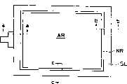
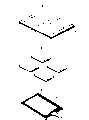
图2是一分解的透视图,说明了根据本发明装在屏幕输入型显示装置中的触摸板的第一个实施例的示意结构。本实施例中的触摸板具有玻璃的膜状上基片1和下基片2。上基片1在其内表面有一上电阻膜3,下基片2也在其内表面有一下电阻膜4。上下基片1和2通过粘接材料8A至8D互相面对齐。FIG. 2 is an exploded perspective view illustrating a schematic structure of a first embodiment of a touch panel incorporated in a screen input type display device according to the present invention. The touch panel in this embodiment has a film-like
上下电阻膜3和4最好是ITO等透明的金属薄膜,但也可用其它导电的透明薄膜。本实施例中,用ITO。此外,用印刷等方式把导电胶如银胶等涂加在各电阻膜的相对端以形成上下布线电极5A、5B和6A、6B。本实施例用银胶。The upper and
此外,从上基片1的输入区(可视区)AR的外围的一侧去掉了与引线连接区10相对应的部分。在这一部分中,输出印刷线路板12被去掉了。印刷线路板12有引线连接上布线电极引线11A、11B和下布线电极引线11C、11D来获取输出信号。从上基片1中去掉的与引线连接区10相对应的部分的形状基本上等同于输出印刷线路板12的连接部分的外形。In addition, a portion corresponding to the
点状垫片9在下基片2的下电阻膜4上形成,以防止上下电阻膜3和4在正常情况下互相接触。垫片9可以用一种所谓的光刻技术形成。也就是说,光敏树脂通过一有预设孔径的遮光膜曝光,使得暴露部分的光敏树脂固化。因此,考虑到防止出现输入操作的不匹配感,上下基片的距离最大为20μm左右。
另一方面,尽管依赖于输入操作工具如笔尖等的尖端的尺寸,如果使用了一半径为0.8mm的普通笔尖状工具,在把一片0.188μm厚的PFT膜用作上基片的情况下,垫片9可能至少要2μm高。而且相邻的垫片9之间的距离最好设定为约1.5mm。因此,垫片9的高度最好设定在2μm至20μm范围内。垫片9的形状不一定局限于点形,也可以是其它如堤形,条形等其它形状,只要它们的形状不对输入操作造成障碍就行。On the other hand, although depending on the size of the tip of the input operation tool such as a pen point, if a common pen point-like tool with a radius of 0.8 mm is used, in the case of using a 0.188 μm thick PFT film as the upper substrate,
这样,上下基片2和3通过它们边缘的粘接材料8A至8D使得他们互相成面对面平行排列。在这个实施例中,粘接材料8A至8D用的是双面胶带。但是,胶粘剂或压敏胶粘剂可用来代替双面胶带。Thus, the upper and
如图2中所示,上布线电极5A和5B装在上基片1的内表面上,它们装在上电阻膜3的左右相对的两个末端上。下布线电极6A和6B装在形成在下基片2的内表面上的下电阻膜4的上下两个对立的方向的末端部分上。As shown in FIG. 2,
上布线电极5A和5B分别同形成在下基片2上的基片互联电极7A和7B建立电连接。这种电连接是通过部分插入粘接材料8C和8D的导电胶8CH和8DH(在这儿是银胶)来实现的。The
从基片互联电极7A上引出的上布线电极引线11A和从基片互联电极7B上引出的上布线电极引线11B共同被引出到输出印刷线路板12的引线连接区10中。The upper
分别从同下电阻膜4相连的下布线电极6A和6B上引出的上布线电极引线11C和11D也引出到输出印刷线路板12的引线连接区10中。The upper wiring electrode leads 11C and 11D respectively drawn out from the
因此,上电阻膜3,上布线电极5A和5B,导电胶8CH和8DH,基片互联电极7A和7B以及上布线电极引线11A和11B就互相之间建立了电连接。Accordingly, the upper
用同样的方式,下电阻膜4,下布线电极6A和6B,下布线电极引线11C和11D也建立了电连接。In the same manner, the lower
图3是一个主体部分平面图,它用来解释一个图2中所解释的触摸板的引线连接区结构的典型例子。其中,从上基片的这一面可以看见下基片。另外,图4是图3沿A—A线的剖面图,图5是图3沿B—B线的剖面图。在图3至5中,与图2中具有相同作用的部分被分别对应的加以引用(下面将要描述的图也适用本原则)。FIG. 3 is a main body plan view for explaining a typical example of the structure of the lead connection area of the touch panel explained in FIG. 2. FIG. Wherein, the lower substrate can be seen from the side of the upper substrate. In addition, FIG. 4 is a cross-sectional view along line AA of FIG. 3 , and FIG. 5 is a cross-sectional view along line BB of FIG. 3 . In FIGS. 3 to 5 , parts having the same functions as those in FIG. 2 are referenced correspondingly (this principle also applies to the figures to be described below).
输出印刷线路板12装在沿板面互相面平行的上基片1和下基片2中位置较低的下基片2的引线连接区10上。金属线13形成在输出印刷线路板12中的一个插入层。金属线13的开放端部分正对下基片2,并且同布线电极引线11的末端通过一种导电连接材料14相连。The output printed
上布线电极和下布线电极的引线11A至11D都引出到下基片2的引线连接区10,并且同输出印刷线路板12相连。上布线电极和下布线电极11B和11D的布线电极引线11B′和11D′被安装在平行于引线连接区10所在的一侧上。然后,布线电极引线11B′和11D′从输出印刷线路板12的侧面引入。The
如图4中所示,在输入区AR的外围,一种粘接材料8C被放置于在一个同输入区AR相隔离的密封部分SL上,SL与AR隔开了一个情性区域NR。上布线电极5A和基片互联电极7A用密封部分SL中的绝缘层15和16包起来。绝缘层15和16不是必需的,但是最好有它们,以防止在潮湿等环境下上布线电极5A和基片互联电极7A发生氧化之类的变质。As shown in FIG. 4, at the periphery of the input area AR, an
顺便提及,图4中所所示的惰性区NR的建立是考虑到由于上下基片间的间隙引起的部分区域不能输入操作。在惰性区域NR,正如下面将要描述的减压装置17是用来避免对上电阻膜3或者上基片1造成破坏。减压装置17形成一个类似于垫片9的点形或堤形的突出材料。Incidentally, the inert region NR shown in FIG. 4 is established in consideration of a part of the region which cannot be inputted due to the gap between the upper and lower substrates. In the inert region NR, a
图5解释了一个结构的例子,在该结构中,在上基片1的内表面形成的上布线电极5A(5B)同在下基片2的内表面形成的基片互联电极7A(7B)建立电连接。上布线电极5A(5B)与基片互联电极7A(7B)通过插入粘接材料8C(8D)的带电导电胶8CH(8DH)建立电连接。导电胶8CH(8DH)最好选用银胶。FIG. 5 explains an example of a structure in which an
根据此实施例的结构,不必考虑因为输出印刷线路板12夹在上下基片之间使得上基片突起而引起的输入错误。因此,使用厚的印刷线路板成为可能。另外,有一些布线电极引线沿着有引线连接区10的一侧从印刷线路板侧面引入。这样可使框架变得窄一些。According to the structure of this embodiment, there is no need to consider input errors due to the output printed
另外,上基片1上与引线连接区10相对应的部分被切除。因此,就不用在上、下基片1、2之间插入输出印刷线路板12了;这样就可以提高生产效率。In addition, a portion of the
图6是一个典型的平面图,它用来说明按照本发明装在屏幕输入型显示装置上的触摸板的框架狭窄效应。如图6中所示传统触摸板的引线连接区10内的布线电极引线引到输出印刷线路板前末端的前面。FIG. 6 is a typical plan view illustrating the frame narrowing effect of a touch panel mounted on a screen input type display device according to the present invention. As shown in FIG. 6, wiring electrode leads in the
这样,需要在下基片2中有一个空隙以保证引线连接区10,从而使得窄化框架有一个限制。Thus, a void is required in the
图7是一个示意图,它用来解释按照本发明装在屏幕输入型显示装置上的触摸板的第二实施例的示意结构。图7(a)是一个透视图。图7(b)是图7(a)沿箭头C方向的侧视图。在这个实施例的触摸板中,将一个包括引线连接区10的上基片从整个面上去掉。另外,在引线连接区10中的布线电极引线11B和11D的前末端11B′和11D′被放置于与引线连接区10存在的一侧平行。这样,前末端部分11B′和11D′分别从侧面引入一个输出印刷线路板12上。Fig. 7 is a diagram for explaining the schematic structure of a second embodiment of a touch panel mounted on a screen input type display device according to the present invention. Fig. 7(a) is a perspective view. Fig. 7(b) is a side view of Fig. 7(a) along the arrow C direction. In the touch panel of this embodiment, an upper substrate including the
顺便提及,所有的布线电极引线11A至11D的前端部分11A′、11B′、11C′、11D′都可以放置于与引线连接区10存在的一侧平行。这样,所有前端部分从11A′至11D′都分别从侧面引入输出印刷线路板12上。Incidentally, the
按照本实施例,不必考虑因为输出印刷线路板12夹在引线连接区10内上下基片1、2之间使得上基片1突起而引起的输入错误。这样,使用一个厚的印刷线路板成为可能。另外,一部分或全部布线电极引线的前端部分沿引线连接区10存在的一侧平行引出。这样使得用第一个实施例中所用的方法来窄化框架成为可能。According to this embodiment, there is no need to consider input errors due to the output printed
图8是一个示意图,它用来解释按照本发明装在屏幕输入型显示装置上的触摸板的第三个实施例的示意结构。如在本发明第二个实施例中所描述,并且在图7中所述的上基片1的移去不在这个实施例中进行。Fig. 8 is a diagram for explaining the schematic structure of a third embodiment of a touch panel mounted on a screen input type display device according to the present invention. As described in the second embodiment of the present invention, and the removal of the
与图7中同样的方式,布线电极输出终端11D的布线电极引线11D′的一部分被放置于与引线连接区10存在的一侧平行。于是,布线电极引线11D′从输出印刷线路板12的侧面引入,因此,向上下基片间的输出印刷线路板引入的布线电极引线避免了在一个地方集中。从而,同图6中所示的例子中所有的布线电极引线11A至11D都集中在一块并引到输出印刷线路板12的前面相比,上基片1的突出量GA降低了。这样,防止了湿度之类的因素进入引线连接区10,从而框架变窄了。In the same manner as in FIG. 7, a part of the
另外,如果减小输出印刷线路板12的厚度,上部基片1的突出量GA会进一步降低。In addition, if the thickness of the output printed
图9是一个示意图,它用来解释按照本发明装在屏幕输入型显示装置上的触摸板的第四个实施例的示意结构。图9(a)是将触摸板作为整体的的剖面图,图9(b)是图9(a)中D部分的放大视图。这个实施例提供了一种避免因为使用环境的改变而导致上基片上1的表面平滑性变化的方法。Fig. 9 is a diagram for explaining the schematic structure of a fourth embodiment of a touch panel mounted on a screen input type display device according to the present invention. FIG. 9( a ) is a sectional view of the touch panel as a whole, and FIG. 9( b ) is an enlarged view of part D in FIG. 9( a ). This embodiment provides a method for avoiding changes in the surface smoothness of the
在这个实施例中,密封部分在上基片1与下基片2相连的剖面从输入区那一面略微向外倾斜。在图9(b),与图2中引线连接区10相对的一面通过例子来表示。In this embodiment, the section of the sealing portion where the
在这个密封部分中,银胶18用在下基片2的基片互联电极7B上,使得它能够隆起。绝缘材料19用在银胶18上,使得银胶18的外部要比内部厚。粘接材料20进一步用到绝缘材料19上。In this sealing portion, silver paste 18 is applied to the
上基片1从箭头方向压到绝缘材料19上,从而能粘在那儿。这样,上基片1被施加了张力从而使得输入区域与下基片2保持平行。The
顺便提及,密封部分的结构并不限于上面所述。任何其他合适的结构都可以用来给上基片1施加张力。例如:银胶18的许多线和点、绝缘材料19或粘接材料20都可以应用或加以标记,从而使它们伸向外面的高度逐渐降低。这样的粘接结构也可用于其他面上。Incidentally, the structure of the sealing portion is not limited to the above. Any other suitable structure can be used to apply tension to the
根据本实施例,上基片1的表面平滑性能经常保持,从而防止由于上基片1的松弛而产生的输入不匹配的感觉。According to the present embodiment, the surface smoothness of the
图10是一个示意图,它用来解释按照本发明装在屏幕输入型显示装置上的触摸板的第五个实施例的示意结构。图10是一个平面视图,它用来解释触摸板的输入区最外部边缘的惰性区域。图11是图10沿a-a线的剖面图,图12是图10沿b-b线的剖面图,图13是图10沿c-c线的剖面图。在图10至图13中,同上面所提到的实施例中的视图中功能相同的部分对应地进行了引用。Fig. 10 is a diagram for explaining the schematic structure of a fifth embodiment of a touch panel mounted on a screen input type display device according to the present invention. Fig. 10 is a plan view for explaining the inert area at the outermost edge of the input area of the touch panel. Fig. 11 is a sectional view of Fig. 10 along line a-a, Fig. 12 is a sectional view of Fig. 10 along line b-b, and Fig. 13 is a sectional view of Fig. 10 along line c-c. In FIGS. 10 to 13 , parts with the same functions as those in the views of the above-mentioned embodiments are referenced correspondingly.
在图10所示的触摸板10中,有一个覆盖触摸板输入区的最外边缘的密封部分SL,并且,在密封部分SL和输入区AR之间有一个情性区NR如图13所示。In the
在惰性区NR中,通过印刷或类似方法装上了一个减压装置17以避免上基片1弯曲太厉害。顺便提及,在这个实施例中,上布线电极5A和5B与基片互联电极7A和7B通过一条双面导电胶带21分别紧密的连在一起。In the inert region NR, a
然而,即使有这样一个减压装置17,上下基片之间大的间隙也有可能导致形成在上基片内表面上的上电阻膜发生破裂或上基片本身遭到破坏。However, even with such a
图14是一个用来解释在上下基片之间有大的间隙时产生缺陷的主要部分的剖视图。图14对应于前面描述过的图13。下布线电极6A、上布线电极引线11B、绝缘材料16和减压装置17装在下基片2的周边上。上基片1通过粘接材料8A与下基片2紧密固定在一起。Fig. 14 is a sectional view of a main part for explaining that a defect occurs when there is a large gap between upper and lower substrates. FIG. 14 corresponds to FIG. 13 described above. On the periphery of the
当通过使用笔尖56末端按压上基片1执行输入操作时,使得上电阻膜3同下电阻膜4相接触,上基片1在它通过粘接材料8A与下基片2相连的地方向下基片2弯曲。When an input operation is performed by pressing the
上基片1在A部分中,向粘接材料8A的末端弯曲,在C部分中同减压装置17部分接触,在B部分中同下电阻膜4部分接触。在这些受到弯曲的部分中,上电阻膜3的破裂或上基片本身遭到破坏都很容易发生。特别的,这种破裂或破坏倾向于出现在A部分即粘接材料8A的末端部分。顺便提及,标号22所指的是一个装置的盖子。The
为了防止这种破裂或破坏,可以考虑增大减压装置的宽度。但是如果在上下基片间有很大的间隙,减压装置17的宽度就会太大,从而使得框架变宽。In order to prevent such cracking or damage, it may be considered to increase the width of the pressure relief device. But if there is a large gap between the upper and lower substrates, the width of the decompression means 17 will be too large, thereby making the frame wider.
图15是一个示意性剖视图,它用来解释按照本发明装在屏幕输入型显示装置上的触摸板的第六个实施例的主要部分结构,类似于图14。在这个实施例中,通过印刷或类似的方法在下基片3内表面形成的各个层例如下布线电极6A(6B)、上布线电极引线11B等等,厚度被减小,从而减小上下基片之间的间隙。每一层厚度最好在5-20μm之间。FIG. 15 is a schematic sectional view for explaining the main part structure of a sixth embodiment of a touch panel mounted on a screen input type display device according to the present invention, similar to FIG. 14. In this embodiment, the thicknesses of the respective layers formed on the inner surface of the
结果,上基片的弯曲量减小了。这样,减压装置的宽度被减小了,从而使得输入区能够扩大,也就是说,框架可以变窄了。As a result, the amount of warping of the upper substrate is reduced. In this way, the width of the pressure relief device is reduced so that the input area can be enlarged, ie the frame can be narrowed.
图16是一个示意性剖视图,它用来解释按照本发明装在屏幕输入型显示装置上的触摸板的第七个实施例的主要部分结构。在这个实施例中,在上基片1内表面形成的上布线电极5B(5A)和在下基片2内表面形成的基片互联电极7B(7A),在上下基片上是互相错位的。Fig. 16 is a schematic sectional view for explaining the main part structure of a seventh embodiment of a touch panel mounted on a screen input type display device according to the present invention. In this embodiment, the
图16表明了上布线电极5B(5A)与基片互联电极7B(7A)是互相错位的情况。一导电粘接材料8H装在上布线电极5B(5A)和基片互联电极7B(7A)之间,以固定它们。在任何其它一面,有电阻膜或电极而不需要在上下基片之间建立电连接的部分,在上下基片间装一绝缘粘接材料以固定它们。FIG. 16 shows the situation that the
按照这种结构,即使在上下基片上形成的各种电极被设成同相关工艺中的一样厚,上下基片1和2之间的间隙也能被缩小。另外,在这样一种结构中,不仅使得省略减压装置的安装成为可能,也使得窄化框架成为可能。According to this structure, the gap between the upper and
按照上面提到的实施例完全可能得到一种没有输入不灵的现象并且尺寸和厚度大大减小的触摸板。According to the above-mentioned embodiment, it is entirely possible to obtain a touch panel free from input malfunction and greatly reduced in size and thickness.
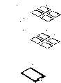
接下来将要描述一种根据本发明生产一种用在屏幕输入型显示装置上的触摸板的方法。Next, a method of producing a touch panel used in a screen input type display device according to the present invention will be described.
图17是一个流程图,它用来解释按照本发明生产一种用在屏幕输入型显示装置上的触摸板的方法的例子。图17包括左手边用来解释下基片生产步骤的步骤集A,右上面用来解释上基片生产步骤的步骤集B以及右下面用来说明组装上下基片的生产步骤的步骤集C。这些步骤表明上下基片是通过双面胶带粘接在一起的,而上布线电极和基片互联电极是通过导电双面胶带建立电连接的。Fig. 17 is a flowchart for explaining an example of a method of producing a touch panel used in a screen input type display device according to the present invention. 17 includes step set A on the left hand side for explaining the production steps of the lower substrate, step set B on the upper right explaining the production steps of the upper substrate, and step set C on the lower right explaining the production steps of assembling the upper and lower substrates. These steps show that the upper and lower substrates are bonded together through double-sided tapes, and the upper wiring electrodes and substrate interconnection electrodes are electrically connected through conductive double-sided tapes.
在步骤集A中一块标准的包括下电阻膜的玻璃基片(玻璃母片),用清洗剂清洗(A-1),然后用印刷机将垫片(这儿是点状垫片)印在基片上(A-2)。将银(Ag)胶印在玻璃基片内表面形成的上电阻膜相对应的末端(A-3)。这样,下布线电极、基片互联电极以及引线都做好了。In step set A, a standard glass substrate (mother glass) including the lower resistive film is cleaned with a cleaning agent (A-1), and then a spacer (here a dot spacer) is printed on the substrate with a printing machine. On-chip (A-2). Silver (Ag) was offset-printed on the inner surface of the glass substrate at the corresponding end of the upper resistive film (A-3). In this way, the lower wiring electrodes, substrate interconnection electrodes and lead wires are all completed.
然后,将绝缘材料印在指定的部分上(A-4),再将用来形成前面所述的惰性区的减压装置印在输入区的周边(A-5)(惰性区印刷也就是减压装置的印刷)。Then, the insulating material is printed on the designated part (A-4), and the decompression device used to form the inert area described above is printed on the periphery of the input area (A-5) (the inert area printing is also the decompression device). press device printing).
接着,用自动敷带机将导电双面胶带粘在上/下导电部分(A-6)(用于上下基片的导电),同时将胶带粘到其它部分上(A-7)(用于上下基片紧密相连的工艺)从而获得一下基片。作为一种替换,应用胶粘剂代替双面胶带的方法也可以接受。Next, use an automatic tape applicator to stick the conductive double-sided tape on the upper/lower conductive part (A-6) (for the conduction of the upper and lower A process in which the upper and lower substrates are closely connected) to obtain the lower substrate. As an alternative, a method of applying an adhesive instead of a double-sided tape is also acceptable.
在步骤集B中,用膜切割机将一块标准的包含上电阻膜的薄膜切割成规定尺寸(母膜大小)(B-1),然后清洗(B-2),退火(B-3)。然后,在上面印刷银胶以形成上布线电极,这样就得到了上基片。顺便提及,当直接在上基片上粘接导电胶制品(如导电双面胶带或其他导电胶带)时,印刷银胶的步骤可以省略。In Step B, a standard film including the upper resistive film is cut into a specified size (mother film size) (B-1) with a film cutting machine, then cleaned (B-2), and annealed (B-3). Then, silver paste was printed on it to form an upper wiring electrode, thus obtaining an upper substrate. Incidentally, when directly bonding conductive adhesive products (such as conductive double-sided adhesive tape or other conductive adhesive tapes) on the upper substrate, the step of printing silver adhesive can be omitted.
在步骤集C中,用(面板)整齐器使完成的上下基片沿板面面对面平行排列(C-1)这样就可以使得它们按照规定的距离连接在一起。粘接完成后,沿板面面对面平行排列的基片用切刀切割到最终的产品尺寸(C-2),然后用清洗剂清洗(C-3)。最后,将一块将成为信号输出终端(输出印刷线路板或所谓的引线部分)的柔软的印刷板(FPC)连接到基片上(C4)。这样,一块触摸板就完成了。将完成的触摸板送到一系列的检测步骤中从而使它能够按照规定的检测项目进行检测。In step set C, the completed upper and lower substrates are aligned face-to-face and parallel along the panel surface (C-1) with a (panel) aligner so that they are joined together at a prescribed distance. After the bonding is completed, the substrates arranged face-to-face and parallel along the board surface are cut to the final product size (C-2) with a cutter, and then cleaned with a cleaning agent (C-3). Finally, a flexible printed board (FPC) which will be a signal output terminal (output printed wiring board or so-called lead part) is connected to the substrate (C4). In this way, a touchpad is completed. The completed touch panel is sent to a series of inspection steps so that it can be inspected according to the specified inspection items.
图18是一个示意图,它用来解释按照本发明的第一个实施例制造用在屏幕输入型显示装置的触摸板的方法。在这个实施例中,上基片1中上电阻膜和上布线电极都形成在一个PET膜的内表面,下基片2中,下电阻膜、下布线电极和上下布线电极引线都形成在一块玻璃片的内表面,上下基片又用双面胶带作为粘接材料紧密粘在一起。FIG. 18 is a diagram for explaining a method of manufacturing a touch panel used in a screen input type display device according to the first embodiment of the present invention. In this embodiment, the upper resistance film and the upper wiring electrodes in the
在图18(a)中,通过层迭一片PET膜基体材料(母膜)和一片玻璃基体材料(玻璃母片)成板面面对面平行排列,可以得到四块触摸板。In Fig. 18(a), four touch panels can be obtained by laminating a piece of PET film base material (mother film) and a piece of glass base material (mother glass sheet) so that the boards are arranged face to face in parallel.
四块触摸板如图18(a)那样成板面面对面平行排列后,用一带有专用刀刃的切刀切割上基片,图18(a)箭头所示方向为切刀在专门切割上基片时的操作路径。顺便提及,图18(b)是图18(a)的侧视图。接着,在下基片后表面画一条同上基片切割线轨迹相同的线,然后如图18(c)所示,破开层迭板,就可得到分别具有输入区AR的四块触摸板作为产品;其它部分是无用部分DIS。切刀可用其它切割装置,如激光光束或其他方法代替。After the four touch panels are arranged face-to-face in parallel as shown in Figure 18 (a), a cutting knife with a special blade is used to cut the upper substrate. operating path. Incidentally, FIG. 18(b) is a side view of FIG. 18(a). Next, draw a line on the rear surface of the lower substrate that is the same as the cutting line track of the upper substrate, and then, as shown in Figure 18(c), break the laminated board to obtain four touch panels with input areas AR respectively as products ; The other part is the useless part DIS. The cutter can be replaced by other cutting means, such as a laser beam or other methods.
另外,上下基片的切割线不一定具有相同的轨迹,但它们应彼此定位很近。Also, the cutting lines of the upper and lower substrates do not have to have the same trajectory, but they should be positioned very close to each other.
因此,通过切割互相粘接在一起的上下基片可以避免由外物导致的污染问题,特别是在切割一块硬板时。此外,上下基片可以互相板面平行对齐或在排列位置和切割位置上紧密相邻。进一步讲,平板排列的工作效率也得到提高。特别是提高了印刷效率。Therefore, the problem of contamination caused by foreign objects can be avoided by cutting the upper and lower substrates bonded to each other, especially when cutting a rigid board. In addition, the upper and lower substrates can be aligned parallel to each other or closely adjacent to each other in the alignment position and the cutting position. Further, the working efficiency of the plate arrangement is also improved. In particular, printing efficiency is improved.
顺便提及,虽然一块层迭板制成四块触摸板的例子已经描述,但是不能说在母膜和玻璃母片允许尺寸范围内可以达到更高的印刷量。By the way, although the example of making four touch panels from one laminate has been described, it cannot be said that a higher printing volume can be achieved within the allowable size range of the mother film and glass mother sheet.
另外,板面整齐排列后切割的制造方法不仅局限于设计在上下基片间具有导电结构和仅仅在一基片上有引线的触摸板相应的这种制造方法,也可用于制造没有基片互联电极或类似装置,并且在上基片上形成的上布线电极引线和在下基片上形成的下布线电极引线分别连接到外边的触摸板。In addition, the manufacturing method of neatly arranging the panels and then cutting them is not limited to the manufacturing method corresponding to the design of a touch panel with a conductive structure between the upper and lower substrates and only leads on one substrate, and can also be used to manufacture interconnect electrodes without substrates. or the like, and the upper wiring electrode leads formed on the upper substrate and the lower wiring electrode leads formed on the lower substrate are respectively connected to the touch panel outside.
图19、20是示意图,它们解释了按照本发明的第二个实施例制造用在屏幕输入型显示装置中的触摸板的方法。在图19、20中的步骤A-1至A-7、B-1至B-4、C-1至C-4分别和图17中的A-1至A-7、B-1至B-4、C-1至C-4对应。19, 20 are diagrams explaining a method of manufacturing a touch panel used in a screen input type display device according to a second embodiment of the present invention. Steps A-1 to A-7, B-1 to B-4, C-1 to C-4 in Fig. 19, 20 are respectively and A-1 to A-7, B-1 to B in Fig. 17 -4, C-1 to C-4 correspond.
在该实施例中,有上电阻膜的上基片的原材料1A被切成预定尺寸(B-1),该标准原材料1A形成滚筒状。引线连接区(此后称“引线部分”)T被去掉,用于粘接输出印刷线路板,上基片原材料1A被清洗(B-2)并经过退火处理(B-3)。In this embodiment, a raw material 1A of an upper substrate having an upper resistive film is cut to a predetermined size (B-1), and the standard raw material 1A is formed into a roll shape. The lead connection area (hereinafter referred to as "lead portion") T is removed for bonding output printed wiring board, and the upper substrate raw material 1A is cleaned (B-2) and annealed (B-3).
然后,在上基片上印刷银(Ag)胶而形成布线电极(B-4)。这样我们就得到了上基片(母膜)的基体。Then, silver (Ag) paste was printed on the upper substrate to form wiring electrodes (B-4). In this way we have obtained the matrix of the upper substrate (mother film).
另一方面,将作下基片的标准玻璃基片2A被清洗干净(A-1),在它上面印刷银胶以形成布线电极(A-3、A-4)。然后,印刷点状垫片(A-2),并印刷一个减压部件(A-5)。下一步,用一块导电胶带将上下导电部分粘到一起(A-6)(实现上下基片导电的过程),在另一部分也粘有一块胶带(A-7)(实现上下基片粘结的过程),这样就得到了一块下基片(玻璃母片大小)。On the other hand, the standard glass substrate 2A to be the lower substrate was cleaned (A-1), and silver paste was printed thereon to form wiring electrodes (A-3, A-4). Then, print a dot spacer (A-2), and print a pressure relief part (A-5). In the next step, use a piece of conductive tape to glue the upper and lower conductive parts together (A-6) (the process of realizing the conduction of the upper and lower substrates), and stick a piece of tape (A-7) on the other part (the process of realizing the bonding of the upper and lower substrates) process), so that a lower substrate (mother glass size) is obtained.
上基片和下基片如母膜或玻璃母板一样定位,它们彼此沿板面面对面平行排列并用特定的压力将它们压到一起(C-1),该片-片层合基片被切成单位大小(C-2)并用清洗剂清洗(C-3)。最后,将输出印刷线路板粘接到引线连接区,一块触摸板就完成了(C-4)。The upper substrate and the lower substrate are positioned like a mother film or mother glass, they are arranged face to face parallel to each other along the board surface and pressed together with a specific pressure (C-1), the sheet-sheet laminated substrate is cut into unit size (C-2) and cleaned with detergent (C-3). Finally, the output printed circuit board is bonded to the lead connection area, and a touch panel is completed (C-4).
图21、22是示意图,它们解释了按照本发明的第三个实施例制造用在屏幕输入型显示装置的触摸板的方法。在图21、22中的步骤A-1至A-7、B-1至B-4、C-1至C-4分别和图17中的A-1至A-7、B-1至B-4、C-1至C-4对应。21, 22 are diagrams explaining a method of manufacturing a touch panel used in a screen input type display device according to a third embodiment of the present invention. Steps A-1 to A-7, B-1 to B-4, C-1 to C-4 in Fig. 21, 22 are respectively and A-1 to A-7, B-1 to B in Fig. 17 -4, C-1 to C-4 correspond.
在该实施例中,有上电阻膜的上基片的原材料1A被切成预定尺寸(B-1),该原材料1A原被卷成滚筒状。然后,切好的上基片被清洗(B-2)并经过退火处理(B-3)。然后,在上基片上印刷银胶而形成布线电极(B-4)。这样我们就得到了上基片(母膜)的基体。In this embodiment, a raw material 1A of an upper substrate having an upper resistive film is cut to a predetermined size (B-1), and the raw material 1A is originally rolled into a roll. Then, the cut upper substrate is cleaned (B-2) and annealed (B-3). Then, silver paste was printed on the upper substrate to form wiring electrodes (B-4). In this way we have obtained the matrix of the upper substrate (mother film).
另一方面,将作下基片的标准玻璃基片2A清洗干净(A-1),在它上面印刷银(Ag)胶以形成布线电极(A-3),同时在上面印刷绝缘涂层(A-4)。然后印刷减压部件(A-5)。上述过程完成后,在基片上印刷点状垫片,用一块导电胶带将上下导电部分粘到一起(A-6),在另一部分也粘有一块胶带(A-7),这样就得到了一块下基片(玻璃母片大小)。On the other hand, the standard glass substrate 2A as the lower substrate is cleaned (A-1), silver (Ag) glue is printed on it to form wiring electrodes (A-3), and an insulating coating is printed on it (A-3). A-4). Then the decompression member (A-5) was printed. After the above process is completed, print dot-shaped spacers on the substrate, use a piece of conductive tape to stick the upper and lower conductive parts together (A-6), and stick a piece of tape on the other part (A-7), so that a piece of Lower substrate (mother glass size).
上基片和下基片像母膜或玻璃母板一样定位,它们彼此沿板面面对面平行排列并用预定的压力将它们压到一起(C-1),去掉用于粘接输出印刷线路板的引线连接区(引线部分)T,基片被切成单元面板尺寸(C-2),并进行清洗(C-3)。最后,将输出印刷线路板粘接到引线连接区,一块触摸板就完成了(C-4)。The upper substrate and the lower substrate are positioned like a mother film or a glass mother board, they are arranged face-to-face and parallel to each other along the board surface and pressed together with a predetermined pressure (C-1), and the adhesive used to bond the output printed circuit board is removed. In the lead bonding area (lead portion) T, the substrate is cut to the unit panel size (C-2), and cleaned (C-3). Finally, the output printed circuit board is bonded to the lead connection area, and a touch panel is completed (C-4).
图23、24是根据本发明制作的屏幕输入式显示装置上用的触摸板的第四个实施例的解释示图。在图23、24中的步骤A-1至A-7、B-1至B-4、C-1至C-4分别和图17中的A-1至A-7、B-1至B-4、C-1至C-4对应。23 and 24 are explanatory diagrams of a fourth embodiment of a touch panel used on a screen input type display device made according to the present invention. Steps A-1 to A-7, B-1 to B-4, C-1 to C-4 in Fig. 23, 24 are respectively and A-1 to A-7, B-1 to B in Fig. 17 -4, C-1 to C-4 correspond.
在该实施例中,有上电阻膜的上基片的原材料1A被切成预定尺寸,该原材料1A的形式一般为滚筒状(B-1);然后清洗(B-2)并经过退火处理(B-3)。In this embodiment, the raw material 1A of the upper substrate of the upper resistive film is cut into a predetermined size, and the form of the raw material 1A is generally a roll shape (B-1); then cleaned (B-2) and annealed ( B-3).
然后,在上基片上印刷银(Ag)胶而形成布线电极(B-4),去掉引线部分。这样我们就得到了上基片(母膜)的基体。Then, silver (Ag) glue was printed on the upper substrate to form wiring electrodes (B-4), and the lead part was removed. In this way we have obtained the matrix of the upper substrate (mother film).
另一方面,将作下基片的标准玻璃基片2A清洗干净(A-1),在它上面印刷银(Ag)胶以形成布线电极(A-3),同时在上面印刷绝缘涂层(A-4)。然后印刷点状垫片(A-2)和减压部件(A-5)。下一步,用一块导电胶带将上下导电部分粘到一起(A-6)(实现上下基片导电的过程),在另一部分也粘有一块胶带(A-7)(实现上下基片粘结的过程),这样就得到了一块下基片(玻璃母片大小)。On the other hand, the standard glass substrate 2A as the lower substrate is cleaned (A-1), silver (Ag) glue is printed on it to form wiring electrodes (A-3), and an insulating coating is printed on it (A-3). A-4). Then dot spacers (A-2) and pressure relief parts (A-5) were printed. In the next step, use a piece of conductive tape to glue the upper and lower conductive parts together (A-6) (the process of realizing the conduction of the upper and lower substrates), and stick a piece of tape (A-7) on the other part (the process of realizing the bonding of the upper and lower substrates) process), so that a lower substrate (mother glass size) is obtained.
上基片和下基片如母膜或玻璃母板一样定位,它们彼此沿板面面对面平行排列并用预定的压力将它们粘到一起(C-1),上基片被切成单元面板尺寸,下基片沿上基片的切线切成单元面板尺寸(C-2)。然后将面对面平行排列的基片清洗干净(C-3)。最后,将输出印刷线路板粘接到引线连接区,一块触摸板就完成了(C-4)。The upper substrate and the lower substrate are positioned like mother film or mother glass, they are arranged face-to-face and parallel to each other along the board surface and bonded together with a predetermined pressure (C-1), the upper substrate is cut to the unit panel size, The lower substrate is cut to the cell panel size (C-2) along the tangent of the upper substrate. Then the substrates arranged face to face in parallel are cleaned (C-3). Finally, the output printed circuit board is bonded to the lead connection area, and a touch panel is completed (C-4).
图25、26是根据本发明制作的屏幕输入式显示装置上用的触摸板的第五个实施例的解释示图。在图25、26中的步骤A-1至A-7、B-1至B-4、C-1至C-4分别和图17中的A-1至A-7、B-1至B-4、C-1至C-4对应。25, 26 are explanatory diagrams of a fifth embodiment of a touch panel used on a screen input type display device made according to the present invention. Steps A-1 to A-7, B-1 to B-4, C-1 to C-4 in Fig. 25, 26 are respectively and A-1 to A-7, B-1 to B in Fig. 17 -4, C-1 to C-4 correspond.
有上电阻膜的上基片的原材料1A被切成预定尺寸,该原材料1A原为滚筒状(B-1);然后清洗(B-2)并经过退火处理(B-3)。The raw material 1A of the upper substrate with the upper resistive film is cut to a predetermined size, and the raw material 1A is in the form of a roll (B-1); then cleaned (B-2) and subjected to annealing treatment (B-3).
然后,在上基片上印刷银(Ag)胶而形成布线电极(B-4),这样我们就得到了上基片(母膜)的基体。Then, print silver (Ag) glue on the upper substrate to form wiring electrodes (B-4), so that we have obtained the base of the upper substrate (mother film).
另一方面,将作下基片的标准玻璃基片2A清洗干净(A-1),在它上面印刷银(Ag)胶以形成布线电极(A-3),同时在上面印刷绝缘涂层(A-4)。然后印刷减压部件(A-5)。下一步,印刷点状垫片(A-2),用一块导电胶带将上下导电部分粘到一起(A-6)(实现上下基片导电的过程),在另一部分也粘有一块胶带(A-7)(实现上下基片粘结的过程),这样就得到了一块下基片(玻璃母片大小)。On the other hand, the standard glass substrate 2A as the lower substrate is cleaned (A-1), silver (Ag) glue is printed on it to form wiring electrodes (A-3), and an insulating coating is printed on it (A-3). A-4). Then the decompression member (A-5) was printed. In the next step, print dot-shaped pads (A-2), stick the upper and lower conductive parts together with a piece of conductive tape (A-6) (the process of realizing the conduction of the upper and lower substrates), and stick a piece of tape on the other part (A -7) (the process of realizing the bonding of the upper and lower substrates), so that a lower substrate (the size of the glass mother sheet) is obtained.
上基片和下基片如母膜或玻璃母板一样定位,它们彼此沿板面面对面平行排列并用预定的压力将它们粘到一起。然后,把基片切成一个单元面板尺寸,同时,一个引线连接区域作为不必要的部分被去掉(C-1)。把一个输出印刷线路板粘接到引线连接区(C-4),并切成单元面板尺寸(C-2)。然后将沿版面面对面平行排列的基片清洗干净(C-3),一块触摸板就完成了。The upper substrate and the lower substrate are positioned as a mother film or mother glass, they are arranged face-to-face and parallel to each other along the board surface and they are bonded together with a predetermined pressure. Then, the substrate is cut into a unit panel size, and at the same time, a lead connection area is removed as an unnecessary portion (C-1). An output printed wiring board is bonded to the lead connection area (C-4) and cut to cell panel size (C-2). Then the substrates arranged in parallel face to face along the layout are cleaned (C-3), and a touch panel is completed.
图27、28是根据本发明制作的屏幕输入型显示装置上用的触摸板的第六个实施例的解释示图。在图27、28中的步骤A-1至A-7、B-1至B-4、C-1至C-4分别和图17中的A-1至A-7、B-1至B-4、C-1至C-4对应。27, 28 are explanatory diagrams of a sixth embodiment of a touch panel used on a screen input type display device made according to the present invention. Steps A-1 to A-7, B-1 to B-4, C-1 to C-4 in Fig. 27, 28 are respectively and A-1 to A-7, B-1 to B in Fig. 17 -4, C-1 to C-4 correspond.
在该实施例中,有上电阻膜的上基片的原材料1A被切成预定尺寸,原材料1A的形式一般为滚筒状(B-1);进行清洗(B-2)并经过退火处理(B-3)。然后在上面印刷银(Ag)胶以形成布线电极(B-4),将基片切成单个触摸板大小(B-5)。同时,去掉每一块触摸板的引线连接区(引线部分),用于粘接输出印刷线路板。In this embodiment, the raw material 1A of the upper substrate of the upper resistive film is cut into a predetermined size, and the form of the raw material 1A is generally a drum shape (B-1); cleaning (B-2) and annealing treatment (B-1) -3). Silver (Ag) paste is then printed thereon to form wiring electrodes (B-4), and the substrate is cut into the size of individual touch panels (B-5). At the same time, the lead connection area (lead part) of each touch panel is removed for bonding the output printed circuit board.
另一方面,将作下基片的标准玻璃基片2A清洗干净(A-1),在它上面印刷银(Ag)胶以形成布线电极(A-3),同时在上面印刷绝缘涂层(A-4)。然后印刷减压部件(A-5)和点状垫片。下一步,用一块导电胶带将上下导电部分粘到一起(A-6),在另一部分也粘有一块胶带(A-7),然后,它们分别切成单个触摸板大小(A-8)。On the other hand, the standard glass substrate 2A as the lower substrate is cleaned (A-1), silver (Ag) glue is printed on it to form wiring electrodes (A-3), and an insulating coating is printed on it (A-3). A-4). Then print the decompression part (A-5) and the dot spacer. Next, glue the upper and lower conductive parts together with a piece of conductive tape (A-6), and a piece of tape on the other part (A-7), then cut them each to the size of a single touchpad (A-8).
上基片和下基片被切成单个尺寸,它们彼此沿板面面对面平行排列(C-1)。然后把输出印刷线路板粘接到引线连接区(C-4),然后清洗干净(C-3),这样,一块触摸板就完成了。The upper substrate and the lower substrate are cut to individual sizes, and they are arranged face-to-face and parallel to each other along the plate surface (C-1). Then the output printed circuit board is bonded to the lead connection area (C-4), and then cleaned (C-3), so that a touch panel is completed.
图29、30是根据本发明制作的屏幕输入型显示装置上用的触摸板的第七个实施例的解释示图。在图29、30中的步骤A-1至A-7、B-1至B-4、C-1至C-4分别和图17中的A-1至A-7、B-1至B-4、C-1至C-4对应。29, 30 are explanatory diagrams of a seventh embodiment of a touch panel used on a screen input type display device made according to the present invention. Steps A-1 to A-7, B-1 to B-4, C-1 to C-4 in Fig. 29, 30 are respectively and A-1 to A-7, B-1 to B in Fig. 17 -4, C-1 to C-4 correspond.
在该实施例中,有上电阻膜的上基片的原材料1A被切成预定尺寸,原材料1A的形式一般为滚筒状(B-1);然后清洗(B-2)并经过退火处理(B-3)。然后,在上基片上印刷银(Ag)胶而形成布线电极(B-4),并将基片切成单个触摸板的尺寸(B-5)。同时,去掉每一块触摸板的引线连接区以粘接输出印刷线路板。In this embodiment, the raw material 1A of the upper substrate of the upper resistance film is cut into a predetermined size, and the form of the raw material 1A is generally a roll shape (B-1); then cleaning (B-2) and annealing treatment (B -3). Then, silver (Ag) paste was printed on the upper substrate to form wiring electrodes (B-4), and the substrate was cut into the size of individual touch panels (B-5). At the same time, the lead connection area of each touch panel is removed to bond the output printed circuit board.
另一方面,将作下基片的标准玻璃基片2A清洗干净(A-1),在它上面印刷银(Ag)胶以形成布线电极(A-3),同时在上面印刷绝缘涂层(A-4)。然后印刷减压部件(A-5)和点状垫片(A-2)。然后,用一块导电胶带将上下导电部分粘到一起(A-6),在另一部分上也粘有一块胶带(A-7);它们被切成单个触摸板大小(A-8)。On the other hand, the standard glass substrate 2A as the lower substrate is cleaned (A-1), silver (Ag) glue is printed on it to form wiring electrodes (A-3), and an insulating coating is printed on it (A-3). A-4). Then the decompression part (A-5) and the dot spacer (A-2) are printed. Then, the upper and lower conductive parts were glued together with a piece of conductive tape (A-6), and a piece of tape was also glued on the other part (A-7); they were cut to the size of individual touchpads (A-8).
把输出印刷线路板(引线)粘接到已去除引线连接区的下基片上(C-4)。The output printed wiring board (leads) is bonded to the lower substrate from which the lead connection areas have been removed (C-4).
上基片和下基片被切成单个尺寸,被定位并彼此沿板面面对面平行排列(C-1’)然后清洗干净,这样,就完成了一块触摸板。The upper and lower substrates are cut to individual sizes, positioned and aligned parallel to each other face-to-face along the board (C-1') and then cleaned, thus completing a touch panel.
按照上面描述的相关工艺制作方法的相关步骤,制成触摸板,将触摸板送到检测工序对预定检测项目进行检测。According to the relevant steps of the manufacturing method of the related process described above, the touch panel is manufactured, and the touch panel is sent to the testing process to test the predetermined testing items.
一个应用根据本发明中的触摸板生产工艺生产的屏幕输入型显示装置实施例的整个配置将参考图31、32、33、34A至34D和35作详细描述。The overall configuration of an embodiment of a screen input type display device using the touch panel production process of the present invention will be described in detail with reference to FIGS. 31 , 32 , 33 , 34A to 34D and 35 .
图31是一剖面图,说明了根据本发明实现屏幕输入型显示装置的第一种模式。在该模式中,背景光(照明器)200包括一个导光板201和一个线发光体202,和一个根据上述任何一个实施例生产的触摸板100,它们被装在反射式液晶显示板300。Fig. 31 is a sectional view illustrating a first mode of realizing a screen input type display device according to the present invention. In this mode, the backlight (illuminator) 200 including a
反射层302、保护层303和下部电极(信号电极)304在第一基片301的内表面成形,它是液晶板300的下基片。反射层302是由铝薄片制成的。保护层303是由SiO2或其他类似材料制成的抗反射膜。每一个下部电极都由透明导电膜ITO或类似材料制成的。A reflective layer 302 , a protective layer 303 and a lower electrode (signal electrode) 304 are formed on the inner surface of a first substrate 301 which is a lower substrate of the
另一方面,一个三色(R、G、B)滤色器306,保护膜307和一个上部电极(扫描电极)308在第二基片305(上部玻璃基片)的内表面成形。在滤色器306中,通过向有机树脂膜中加染料或着色剂从而得到三种颜色(R、G、B)。保护层307由有机材料制成,这样可以防止液晶层309被滤色器306污染,并保证第二基片305的内表面平整。上部电极308是由透明导电膜ITO或类似材料制成。On the other hand, a three-color (R, G,
顺便提及,格栅状或条状光阻隔膜(黑色基体)可制成R、G、B任何一种颜色,这样就可根据需要制成滤色器306,保护膜307在光阻隔膜上形成。Incidentally, the grid-shaped or strip-shaped light-blocking film (black matrix) can be made into any color of R, G, and B, so that the
在第一和第二基片301和305之间注射液晶材料形成液晶层309。使用环氧树脂或类似材料作密封材料(310)密封。这样一块液晶显示板就准备好了。A
极化板312b,第一相差片312C和第二相差片312D被层迭在液晶板的第二基片305的表面上。极化板312b,第一相差片312C和第二相差片312D里有由胶粘剂(如:环氧或者丙烯酸胶粘剂)、胶粘材料或类似材料制成的胶粘层311和311a。这样独立构件311a、311b、311c、311d就可以被固定。A
顺便提及,对这种胶粘剂来说,即使各种光学薄膜312b和312d以前的粘接被剥离开,光学薄膜312b和312d也可以重新彼此粘接到一起。用这种胶粘剂粘接312b到312d中的各种光学薄膜或液晶板时,即使312b到312d的光学薄膜或液晶板按装错了,312b到312d中的光学薄膜或液晶板仍可以从新按装,这样产量就会提高。Incidentally, with this adhesive, even if the previous bonding of the various
更可取的,从反射率角度看,反射层302具有镜面反射能力,在该实施例中,反射层302是用铝膜汽相淀渍法制成。为增加反射率,在反射层302的表面一般有多层膜。在多层膜的表面上成形保护膜303,这样可以防止反射层302被腐蚀,并使得反射层302表面的平整。More preferably, from the perspective of reflectivity, the reflective layer 302 has specular reflective ability. In this embodiment, the reflective layer 302 is made by vapor deposition of aluminum film. In order to increase the reflectivity, there are generally multi-layer films on the surface of the reflective layer 302 . A protective film 303 is formed on the surface of the multilayer film, which can prevent the reflection layer 302 from being corroded and make the surface of the reflection layer 302 smooth.
顺便提及,反射膜不仅限于铝材。银、铬或其他的金属膜或非金属膜,如果它们具有镜面反射能力,也可以使用。Incidentally, the reflective film is not limited to aluminum materials. Silver, chrome or other metallic or non-metallic films may also be used if they are specularly reflective.
另外,保护膜303不仅限于SiO2膜。用于保护反射层302的保护膜303最好是绝缘膜。保护膜303可以是无机膜如渗氮硅或其他,有机金属膜如有机钛膜或其他金属膜,也可是聚酰亚胺、环氧或其他有机膜。更可取的是,聚酰亚胺、环氧或其他有机膜有非常优秀的平整性,从而使得下部电极304可以轻易的在保护薄膜303上成形。如果有机金属膜如:有机钛膜或其他类似膜被用于保护膜303,下部电极304可以在高温下成形。这样,就可以降低下部电极304的布线电阻。In addition, the protective film 303 is not limited to the SiO2 film. The protective film 303 for protecting the reflective layer 302 is preferably an insulating film. The protective film 303 can be an inorganic film such as silicon nitride or others, an organic metal film such as organic titanium film or other metal films, or polyimide, epoxy or other organic films. More preferably, polyimide, epoxy or other organic films have excellent flatness, so that the
在液晶板上面,安装多层光学膜的位置,当外部光不足时,可使用一个具有一个导光板201和一个光源202的照明器200。On the liquid crystal panel, where the multilayer optical film is installed, when external light is insufficient, an
导光板由如聚丙烯树酯或其他树脂制成。用于使光L4从光源202射向液晶板的印刷花纹或不规则形状,成形在观测者一边的导光板201的一个表面(上表面)。The light guide plate is made of, for example, polypropylene resin or other resins. Printed patterns or irregular shapes for directing light L4 from the
进一步,触摸板100安装在照明器200之上。当触摸板100的表面被输入操作工具压下时(尖棒状物体如笔尖),指尖或其他,当触摸板100检测到受压部分的位置坐标就输出一个数据信号。数据信号会被传到信息处理设备(图35中的547)的主机系统(图35中的550,将在后面介绍)。Further, the
液晶显示装置300的第二基片305,照明器200的导光板201,触摸板100通过双面胶带(例如胶粘剂浸渍无纺布)或其他材料固定。The
用双面胶带将液晶显示装置300,照明器200和触摸板100粘在一起,它们可以彼此剥离,这样即使按装错误也可复原。The liquid
顺便提及,照明器200不是必须组件。当这种显示装置总在明亮的环境中使用时,不需要照明器200。Incidentally, the
在本实施例中,在第一相差片312c和第二相差片312d之间的胶层311a应有光散射作用。特别的,一种光散射材料的折光指数与它和胶粘剂混合后的折光指数不同。当用环氧类或丙烯酸类之胶粘剂材料时,透明有机物颗粒如聚乙烯、聚丙烯、二乙烯基苯或其他,或透明无机材料颗粒如硅石或其他一些物质可用作光散射材料。In this embodiment, the
顺便提及,具有与光散射材料不同折光指数的胶粘材料可用作前面提到的胶粘材料。在这种情况下,即使第一相差片312c和第二相差片312d装错了,它们仍可回到原来状态。Incidentally, an adhesive material having a different refractive index from that of the light-scattering material can be used as the aforementioned adhesive material. In this case, even if the first phase difference film 312c and the second
当透明有机物颗粒或透明无机物颗粒被用作光散射材料时,可见光部分的光吸收就会降低,这样,液晶板的反射率或光谱特性都会提高。When transparent organic particles or transparent inorganic particles are used as light-scattering materials, the light absorption in the visible light portion will be reduced, so that the reflectance or spectral characteristics of the liquid crystal panel will be improved.
进一步说,当胶粘剂是有机物时,如果有机物颗粒用作光散射材料时,胶粘剂和光散射材料的热膨胀系数的差异可以减小。这样就不用担心胶层311a会破裂。Further, when the adhesive is organic, if organic particles are used as the light-scattering material, the difference in thermal expansion coefficient between the adhesive and the light-scattering material can be reduced. In this way, there is no need to worry about the
顺便提及,当胶粘剂中混有光散射材料时,这种胶层比只含有一种胶粘材料的胶层更容易破裂。然而,包含光散射材料的胶层311a被夹在第一相差片312C和第二相差片312D之间,它们具有基本一致的热膨胀系数。这样,胶层311a破裂的问题就可以避免。Incidentally, when a light-scattering material is mixed in the adhesive, the adhesive layer is more likely to be broken than an adhesive layer containing only one adhesive material. However, the
下面,对图31中结构的显示原理进行描述。入射光L1从不同的方向进入液晶显示装置400,依次通过触摸板100,照明器200的导光板201,极化板312b,把极化板312b固定到第一相差片312c上的胶层311,第一相差片312c,用于固定第一相差片312c到第二相差片312d的有光散射功能的胶层311a,第二相差片312d,用于将第二相差片312d固定到第二基片305上的胶层311,第二基片305,滤色器306,上部电极308,液晶层309,和一个专用的像素电极(或专用信号线)304a,到达反光层302。Next, the display principle of the structure in Fig. 31 will be described. The incident light L1 enters the liquid
外部光L1到达反光层302后,反射形成反射光L2,反射光L2经过一个与入射光L1相反的路径到达胶层311a,该层具有光散射功能。反射光L2入射到胶层311a并在各个方向散射。这样,就产生了在各个方向散射的散射光L3。After the external light L1 reaches the reflective layer 302, it is reflected to form reflected light L2. The reflected light L2 reaches the
直接反射光L2或从胶层311a发出的散射光L3通过第一相差片312c,胶层311,极化板312b,导光板201和触摸板100发射到液晶显示装置400的外边。当直接反射光L2或散射光L3透过液晶板309时出现的相差可由第一相差片312c的双折射效应补偿。The directly reflected light L2 or the scattered light L3 emitted from the
观测者可看到发射出液晶显示装置外面的直接反射光L2或散射光L3,这样,观测者可看到通过这个专用像素电极304a控制的显示。The observer can see the direct reflected light L2 or scattered light L3 emitted from the outside of the liquid crystal display device, so that the observer can see the display controlled by the dedicated pixel electrode 304a.
图32是一个剖面图,它用来解释按照本发明实现一种屏幕输入型显示装置的第二种模式。同图31中具有相同功能的部分相应的进行了引用。在这种模式中,同图31中描述的类似的照明器200层迭到一个液晶显示装置300上,一个触摸板100又安装到照明器200上。这样,一个屏幕输入型液晶显示装置400就安装好了。Fig. 32 is a sectional view for explaining a second mode of realizing a screen input type display device according to the present invention. Parts having the same functions as those in FIG. 31 are cited accordingly. In this mode, an
液晶显示装置300是一个薄膜型晶体管(TFT)类型的液晶板,这是典型的活性基体类型。许多具有薄膜晶体管TFT1和一个像素电极304a的像素形成在组成液晶显示装置300的第一基片301内表面。The liquid
每一个像素安放在由两条相邻的扫描信号线和两条相邻的视频信号线交叉区域内。薄膜晶体管TFT1是由装在第一基片301上的第一半导体层AS(电路层)、安装在第一半导体层AS上的第二半导体层r0(掺杂半导体层)、还有安装在第二半导体层r0上的一个源电极SD1和一个漏电极SD2组成。这儿,由导电膜r1和r2的多层膜形成源电极SD1和漏电极SD2。但是源电极SD1和漏电极SD2也可以只由一层导电膜形成,也就是说只有导电膜r1。Each pixel is placed in the intersection area of two adjacent scanning signal lines and two adjacent video signal lines. The thin film transistor TFT1 is composed of the first semiconductor layer AS (circuit layer) installed on the first substrate 301, the second semiconductor layer r0 (doped semiconductor layer) installed on the first semiconductor layer AS, and the second semiconductor layer installed on the second semiconductor layer AS. It consists of a source electrode SD1 and a drain electrode SD2 on the second semiconductor layer r0. Here, the source electrode SD1 and the drain electrode SD2 are formed of a multilayer film of the conductive films r1 and r2. However, the source electrode SD1 and the drain electrode SD2 may also be formed of only one conductive film, that is, only the conductive film r1.
顺便提及,源电极和漏电极之间的关系可以对应于怎样施加电压而相互转化,也就是说,电极SD2可以作为源电极,而电极SD1可以作为漏电极。但是,在接下来的描述中,为方便起见,电极SD1被认为是源电极,电极SD2被认为是漏电极。Incidentally, the relationship between the source electrode and the drain electrode can be switched to each other corresponding to how the voltage is applied, that is, the electrode SD2 can serve as the source electrode, and the electrode SD1 can serve as the drain electrode. However, in the description that follows, for convenience, the electrode SD1 is regarded as a source electrode, and the electrode SD2 is regarded as a drain electrode.
PSV1代表一种绝缘膜(保护膜),它用来保护薄膜晶体管TFT1;像素电极304a;为了使液晶层309整齐排列而分别与第一基片301和第二基片305紧靠的对准膜ORI1和ORI2;上部电极308(普通电极)。PSV1 represents a kind of insulating film (protective film), which is used to protect the thin film transistor TFT1; pixel electrode 304a; in order to make the
一个又称作黑色基体的光屏蔽膜BM具有屏蔽相邻像素电极304a之间的光的作用,从而增强对比度。一个导电膜310与上部电极308通过安装在第一基片301上的终端(多层金属导电膜g1,g2,r1,r2和r3)建立电连接。A light-shielding film BM, also called a black matrix, has the effect of shielding light between adjacent pixel electrodes 304a, thereby enhancing contrast. A
当一个给定的电压加到栅电极GT上时,源电极SD1和漏电极SD2之间建立了电传导。这样,薄膜晶体管TFT1就可以用与绝缘栅型场效应晶体管同样的方式作一个开关用。When a given voltage is applied to the gate electrode GT, electrical conduction is established between the source electrode SD1 and the drain electrode SD2. Thus, the thin film transistor TFT1 can be used as a switch in the same manner as the insulated gate field effect transistor.
像素电极304a同源电极SD1相连。当扫描信号线同栅电极GT相连时,像素304的视频信号线与漏电极SD2相连。根据加在扫描信号线上的给定电压来选择特殊的像素电极304a,一个加在视频信号线上的渐变电压供给特殊像素电极304a。由导电膜g1形成的电容电极CTS具有保持提供给像素电极304a的渐变电压的功能,直到下一次选择时间的到来。The pixel electrode 304a is connected to the source electrode SD1. When the scanning signal line is connected to the gate electrode GT, the video signal line of the
这样,一个活性基体类型液晶显示装置300对每一个像素都有一个像薄膜晶体管之类的开关元件。相应地说,不同像素间不会产生交调失真的问题,而且也不需要采用特殊的电压平衡驱动或类似方法来抑制交调失真。因此,就可以很容易的得到一个多级显示。另外,活性基体类型液晶显示装置300具有一个特点:即使扫描线数目增加,对比度也不会降低。液晶板不仅仅局限于上面所提的配置,所谓的多晶硅半导体也有可能用在液晶板上。Thus, an active matrix type liquid
在本实施例中,像素电极304a由一个铝、铬、钛、钽、钼、银或其他的反射金属膜形成。另外,保护膜PSV1安装在像素电极304a和薄膜晶体管TFT1之间。因此,就可能实现一种高反射率的液晶板,其中,即使像素电极304a扩大到与薄膜晶体管TFT1交叠的程度,也不用担心会发生机能失灵。In this embodiment, the pixel electrode 304a is formed of an aluminum, chromium, titanium, tantalum, molybdenum, silver or other reflective metal film. In addition, a protective film PSV1 is installed between the pixel electrode 304a and the thin film transistor TFT1. Therefore, it is possible to realize a high-reflectance liquid crystal panel in which there is no fear of malfunction even if the pixel electrode 304a is enlarged to the extent that it overlaps the thin film transistor TFT1.
进一步的讲,在这种液晶板中,虽然没有安装如图31所述类型的液晶板中的第一相差片,但是安装了一个第三相差片312e来增强视角特征。第三相差片312e又称为视角扩展膜,它通过利用双折射特征改善了对液晶板显示特征的角度依赖性。Further, in this liquid crystal panel, although the first phase difference plate in the liquid crystal panel of the type described in FIG. 31 is not installed, a third
第三相差片312e能由聚碳酸脂、聚丙烯酸脂、聚砜或类似聚合物的有机树脂膜形成。相应的,通过使用光散射胶层311a做粘接层将第三相差片312e固定到第二相差片312d上,这样可防止光散射胶层311a破裂。The third
图33有5个视图(a)至(e)解释根据本发明的屏幕输入型显示装置的外型。图(a)是显示表面的主视图;图(b),俯视图;图(c),仰视图;图(d)左视图;图(e),右视图。Fig. 33 has 5 views (a) to (e) for explaining the appearance of the screen input type display device according to the present invention. Figure (a) is the front view of the display surface; Figure (b), top view; Figure (c), bottom view; Figure (d) left view; Figure (e), right view.
在图33的(a)至(e)视图中,上壳(屏蔽箱)318是由不锈钢、铁、铝等材料制成的金属板。上壳318开有第一个开口320作为显示窗口。下壳319是由不锈钢、铁、铝等金属材料制成的金属板或由聚碳酸脂,ABS树脂等塑料制成的塑料板。In views (a) to (e) of FIG. 33 , the upper case (shielding box) 318 is a metal plate made of stainless steel, iron, aluminum, or the like. The upper shell 318 has a first opening 320 as a display window. The lower shell 319 is a metal plate made of metal materials such as stainless steel, iron, aluminum or a plastic plate made of polycarbonate, ABS resin and other plastics.
上壳318设有爪子321和钩子322。下壳319通过爪子321和钩子322固定以使下壳319和上壳318结合。The upper case 318 is provided with claws 321 and hooks 322 . The lower case 319 is fixed by claws 321 and hooks 322 to combine the lower case 319 and the upper case 318 .
照明系统200(这儿指,前灯)由导光板201和光源(灯)202如荧光灯,发光二极管等组成,当外界光线不足时它用来照亮液晶显示装置300。导光板201由丙烯酸树脂,玻璃等透明材料制成的。标号100代表用来输入数据到主机系统(信息处理部分)的触摸板,主机系统与液晶显示装置400相连。The lighting system 200 (here, the front light) is composed of a
光学膜312如散光层、极化板、相差板等安装在液晶显示装置400的显示部分。光学膜312安装在上壳318的开口区域内以使液晶显示装置400的整体厚度减小。An optical film 312 such as a light-scattering layer, a polarizing plate, a phase difference plate, etc. is mounted on the display portion of the liquid
图34A至34D是图33的主要部位的剖面图。图34A是图33的视图(a)中沿A-A线的剖面图;图34B是图33的视图(a)中沿B-B线的剖面图;图34C是图33的视图(a)中沿C-C线的剖面图;图34D是图33的视图(a)中沿D-D线的剖面图。34A to 34D are sectional views of main parts of FIG. 33 . Fig. 34A is a sectional view along the A-A line in the view (a) of Fig. 33; Fig. 34B is a sectional view along the B-B line in the view (a) of Fig. 33; Fig. 34C is a sectional view along the C-C line in the view (a) of Fig. 33 Figure 34D is a cross-sectional view along line D-D in view (a) of Figure 33.
在液晶板上,在液晶注射到第一和第二基片301和305的缝隙(这个缝隙用来使第一基片301和第二基片305相互面对齐)中之后,用密封物331密封注射孔。开在上壳318上的开口323与密封物331对应,以使得即使密封物伸到外面也能防止液晶板的外尺寸增大。On the liquid crystal panel, after the liquid crystal is injected into the gap between the first and second substrates 301 and 305 (this gap is used to align the first substrate 301 and the
印刷线路板(扫描线驱动印刷线路板)330装有一用于驱动扫描线的扫描线驱动集成电路芯片328,它装在第一和第二基片301和305的外围。印刷线路板330通过一柔软的印刷线路板329与液晶板相连。A printed wiring board (scanning line driving printed wiring board) 330 is provided with a scanning line driving integrated circuit chip 328 for driving scanning lines, which is mounted on the periphery of the first and
此外,印刷线路板(信号线驱动印刷线路板)333装有一用于驱动信号线的信号线驱动集成电路芯片332,它装在第一和第二基片301和305的外围。印刷线路板333有一柔软的印刷线路板329与液晶板相连。In addition, a printed wiring board (signal line driving printed wiring board) 333 is provided with a signal line driving integrated circuit chip 332 for driving signal lines, which is mounted on the periphery of the first and
用于显示的各种信号和电压通过界面连接器324由外线路(主机系统)提供给扫描线驱动印刷线路板330和信号线驱动印刷线路板333。顺便提及,界面连接器324装在扫描线驱动印刷线路板330上。但是,界面连接器324也可装在信号线驱动印刷线路板333上。Various signals and voltages for display are supplied to the scanning line driving printed wiring board 330 and the signal line driving printed wiring board 333 from the external line (host system) through the
垫片326固定扫描线驱动印刷线路板330,而垫片327固定扫描线驱动印刷线路板330和信号线驱动印刷线路板333的连接部分,和固定扫描线驱动印刷线路板330和液晶板的连接部分;垫片326和327是由绝缘弹性材料如橡胶等制成的。The spacer 326 fixes the scanning line driving printed circuit board 330, and the spacer 327 fixes the connecting part of the scanning line driving printed wiring board 330 and the signal line driving printed wiring board 333, and fixes the connection between the scanning line driving printed wiring board 330 and the liquid crystal panel. Part; gaskets 326 and 327 are made of insulating elastic material such as rubber or the like.
标号325代表一双面胶带;例如,浸渍环氧胶粘剂的无纺布可以用做双面胶带325。利用双面胶带325,上壳318固定在液晶板上,液晶板的上壳固定在照明器200的导光板201上,照明器200的导光板201固定在触摸板100上。Reference numeral 325 represents a double-sided tape; for example, a non-woven fabric impregnated with epoxy adhesive can be used as the double-sided tape 325 . The upper case 318 is fixed on the liquid crystal panel by double-sided adhesive tape 325 , the upper case of the liquid crystal panel is fixed on the
以这种方式,即用双面胶带325把辅助光源系统和触摸板固定到液晶板上,简化了装配工序,并且在错误装配的情况下,恢复组件也变得容易。这样,提高了生产效率。In this way, the auxiliary light source system and the touch panel are fixed to the liquid crystal panel with the double-sided tape 325, the assembly process is simplified, and in the case of wrong assembly, it becomes easy to restore the assembly. In this way, production efficiency is improved.
在下壳319中形成一个向内突起的部分319a,下壳319把液晶板和上壳318连在一起。液晶板由突起部分319a压紧固定。An inwardly protruding portion 319a is formed in the lower case 319, which connects the liquid crystal panel and the upper case 318 together. The liquid crystal panel is pressed and fixed by the protruding portion 319a.
图35是一解释图,说明了使用基于本发明的屏幕输入型显示装置的信息处理设备的一个例子。该信息处理设备也称之为便携式信息终端,它是由主体部分547和显示部分548组成的。主体部分547包括一键盘549和主机系统(信息处理部分)550,主机系统包括微型机算计551和电池552。Fig. 35 is an explanatory diagram illustrating an example of an information processing apparatus using a screen input type display device based on the present invention. This information processing device is also called a portable information terminal, and is composed of a
显示部分548与前面所述的按压输入型液晶显示装置400安装在一起。字符或图形558用放在存笔部分557的笔556输入到显示部分中的触摸板。另外,用笔556选定插图559。The
另外,显示部分548与一通过电缆555给辅助光源系统提供照明电力的变换器电源554安装在一起In addition, the
来自主体部分的显示信号或电压通过一界面电缆553提供给液晶板的界面连接器324,液晶板组成装在显示部分548上的液晶显示装置400。The display signal or voltage from the main part is supplied to the
而且,该信息处理设备可以通过电缆561与便携式电话560相连。这样,信息处理设备可以与信息通信网络如互连网等相连,以获得信息。Also, the information processing device can be connected to a
这样,通过使用本发明的屏幕输入型显示装置,信息处理设备的尺寸和重量减小使其可用性得到改善。Thus, by using the screen input type display device of the present invention, the information processing apparatus can be reduced in size and weight so that its usability can be improved.
顺便提及,这样的便携式信息终端的外型或结构不限于已说明的这个。便携式信息终端可以考虑采取与已说明的例子不同的各种外型,结构及具有各种功能。Incidentally, the appearance or structure of such a portable information terminal is not limited to the one described. It is conceivable for the portable information terminal to take various appearances, structures, and functions different from the examples described above.
如上所述,根据本发明,用在屏幕输入型显示装置的触摸板可以避免由于从上下基片间抽取输出线的区域,也就是,输出印刷线路板安装的区域隆起所引起的显示失真或输入错误。另外,避免了触摸板的整个尺寸增大。因此,触摸板的整体尺寸和重量减小,并且具有狭窄的框架结构。这样,可以很容易的增大输入区的可视面积。此外,可以防止由于重复输入操作引起的上基片上的电阻膜或上基片自身的破坏。这样,就有可能提供一高可靠性的屏幕输入型显示装置。另外,就有可能实现高效率的生产方法,并可以防止异物污染。As described above, according to the present invention, the touch panel used in the screen input type display device can avoid display distortion or input due to the area where the output line is extracted from between the upper and lower substrates, that is, the area where the output printed wiring board is mounted rises. mistake. In addition, an increase in the overall size of the touch panel is avoided. Therefore, the overall size and weight of the touch panel are reduced, and it has a narrow frame structure. In this way, the viewable area of the input area can be easily increased. In addition, damage to the resistive film on the upper substrate or the upper substrate itself due to repeated input operations can be prevented. Thus, it is possible to provide a highly reliable screen input type display device. In addition, it is possible to realize a high-efficiency production method, and foreign matter contamination can be prevented.
Claims (22)
Translated fromChineseApplications Claiming Priority (4)
| Application Number | Priority Date | Filing Date | Title |
|---|---|---|---|
| JP194112/2000 | 2000-06-28 | ||
| JP2000194112 | 2000-06-28 | ||
| JP59515/2001 | 2001-03-05 | ||
| JP2001059515AJP2002082772A (en) | 2000-06-28 | 2001-03-05 | Touch panel, method of manufacturing the same, and screen input type display device using the touch panel |
Publications (1)
| Publication Number | Publication Date |
|---|---|
| CN1333477Atrue CN1333477A (en) | 2002-01-30 |
Family
ID=26594843
Family Applications (1)
| Application Number | Title | Priority Date | Filing Date |
|---|---|---|---|
| CN01125463APendingCN1333477A (en) | 2000-06-28 | 2001-06-28 | Touch pad, method for making same, and screen input type indicator using same |
Country Status (5)
| Country | Link |
|---|---|
| US (1) | US20020000979A1 (en) |
| JP (1) | JP2002082772A (en) |
| KR (1) | KR20020001638A (en) |
| CN (1) | CN1333477A (en) |
| TW (1) | TW581917B (en) |
Cited By (9)
| Publication number | Priority date | Publication date | Assignee | Title |
|---|---|---|---|---|
| CN1307528C (en)* | 2002-12-24 | 2007-03-28 | Lg.飞利浦Lcd有限公司 | Touch panel and manufacturing method thereof, liquid crystal display device and manufacturing method thereof |
| CN101406989B (en)* | 2008-11-11 | 2011-05-25 | 深圳市大族激光科技股份有限公司 | Laser cutting method of touch screen |
| CN102414650A (en)* | 2009-05-11 | 2012-04-11 | 京瓷株式会社 | Touch panel and display device provided with same |
| CN101515212B (en)* | 2007-10-03 | 2012-05-09 | 苹果公司 | Touch sensor panel and its manufacture method |
| CN102479019A (en)* | 2010-11-22 | 2012-05-30 | 财团法人工业技术研究院 | Flexible resistance type touch sensor |
| CN102778971A (en)* | 2006-12-15 | 2012-11-14 | 苹果公司 | Pet-based touchpad |
| CN102084323B (en)* | 2008-03-03 | 2013-07-17 | 星电株式会社 | Touch panel |
| CN103543862A (en)* | 2012-07-13 | 2014-01-29 | 永恒科技有限公司 | Touch screen and manufacturing method thereof |
| CN103676310A (en)* | 2012-09-12 | 2014-03-26 | 元太科技工业股份有限公司 | Display device |
Families Citing this family (85)
| Publication number | Priority date | Publication date | Assignee | Title |
|---|---|---|---|---|
| KR100522528B1 (en) | 2000-10-13 | 2005-10-19 | 가부시키가이샤 덴소 | Touch panel and display device |
| US20030048597A1 (en)* | 2001-09-07 | 2003-03-13 | Shih-Chieh Wang | Personal digital assistant with waterproof and dustproof functions |
| KR100487356B1 (en)* | 2001-12-17 | 2005-05-03 | 엘지.필립스 엘시디 주식회사 | Method of forming signal line of touch panel |
| TWI262034B (en)* | 2002-02-05 | 2006-09-11 | Semiconductor Energy Lab | Manufacturing system, manufacturing method, method of operating a manufacturing apparatus, and light emitting device |
| TWI285515B (en)* | 2002-02-22 | 2007-08-11 | Semiconductor Energy Lab | Light-emitting device and method of manufacturing the same, and method of operating manufacturing apparatus |
| JP2003288166A (en)* | 2002-03-27 | 2003-10-10 | Fujitsu Component Ltd | Connection structure between touch panel and external lead wire |
| JP3824220B2 (en)* | 2002-04-30 | 2006-09-20 | ホシデン株式会社 | Touch panel electrode connection structure |
| JP4104489B2 (en) | 2002-05-17 | 2008-06-18 | 東芝松下ディスプレイテクノロジー株式会社 | Display device and manufacturing method thereof |
| US7126589B2 (en)* | 2002-05-29 | 2006-10-24 | Au Optronics Corporation | Touch control panel |
| JP4032857B2 (en) | 2002-07-24 | 2008-01-16 | ソニー株式会社 | Glass substrate for touch panel, touch panel and portable terminal |
| DE10237119B3 (en)* | 2002-08-13 | 2004-04-15 | Fujitsu Siemens Computers Gmbh | display device |
| KR100510721B1 (en)* | 2002-11-14 | 2005-08-30 | 엘지.필립스 엘시디 주식회사 | touch panel for display device |
| KR100519370B1 (en) | 2002-12-24 | 2005-10-07 | 엘지.필립스 엘시디 주식회사 | Method for Forming Touch Panel with Polarizer Layer |
| AU2003300428A1 (en)* | 2002-12-31 | 2004-08-13 | Motorola, Inc. | Multi-layer laminated user interface |
| US20040169643A1 (en)* | 2003-02-27 | 2004-09-02 | Kuo-Hao Tseng | Touch panel and method for fabricating the same |
| JP4313089B2 (en) | 2003-05-23 | 2009-08-12 | 富士通テン株式会社 | Radar apparatus for automobile and its mounting direction adjusting method |
| WO2005017732A1 (en)* | 2003-08-18 | 2005-02-24 | Gunze Limited | Transparent touch panel and electronic apparatus |
| JP4303167B2 (en)* | 2004-06-11 | 2009-07-29 | アルプス電気株式会社 | Input device |
| US7113179B2 (en)* | 2004-06-23 | 2006-09-26 | Interlink Electronics, Inc. | Force sensing resistor with calibration element and method of manufacturing same |
| TWI278690B (en)* | 2004-06-25 | 2007-04-11 | Hannstar Display Corp | Input-sensor-integrated liquid crystal display panel |
| JP2006099247A (en)* | 2004-09-28 | 2006-04-13 | Nippon Sheet Glass Co Ltd | Thin touch panel and its manufacturing method |
| US20060181521A1 (en)* | 2005-02-14 | 2006-08-17 | Atrua Technologies, Inc. | Systems for dynamically illuminating touch sensors |
| JP2006285417A (en)* | 2005-03-31 | 2006-10-19 | Fujitsu Component Ltd | Touch panel |
| KR20060116102A (en)* | 2005-05-09 | 2006-11-14 | 삼성전자주식회사 | Backlight Assembly and Display Device Having Same |
| JP2007018226A (en)* | 2005-07-07 | 2007-01-25 | Three M Innovative Properties Co | Touch panel sensor |
| WO2007037795A2 (en)* | 2005-08-05 | 2007-04-05 | Amgen Inc. | Stable aqueous protein or antibody pharmaceutical formulations and their preparation |
| JP4694388B2 (en)* | 2006-02-28 | 2011-06-08 | 任天堂株式会社 | Input device using touch panel |
| JP4285504B2 (en)* | 2006-05-24 | 2009-06-24 | ソニー株式会社 | Display device having touch panel |
| GB0611032D0 (en)* | 2006-06-05 | 2006-07-12 | Plastic Logic Ltd | Multi-touch active display keyboard |
| KR100843617B1 (en)* | 2006-07-10 | 2008-07-04 | 아이티엠 주식회사 | Resistive type touch screen in and its manufacturing method |
| JP4809783B2 (en)* | 2007-01-26 | 2011-11-09 | 株式会社 日立ディスプレイズ | Display module with touch panel |
| JP4442648B2 (en)* | 2007-06-28 | 2010-03-31 | ミツミ電機株式会社 | Panel switch manufacturing method and panel switch |
| CA2703666A1 (en)* | 2007-10-31 | 2009-05-07 | Yasuji Kusuda | Protection panel with touch input function for display window of electronic device, and electronic device |
| JP5196973B2 (en)* | 2007-11-27 | 2013-05-15 | 富士通コンポーネント株式会社 | Electronic equipment with panel-type input device |
| JP5014230B2 (en)* | 2008-04-01 | 2012-08-29 | 京セラ株式会社 | Touch panel and touch panel display device |
| KR100871329B1 (en)* | 2008-04-23 | 2008-12-01 | 주식회사 옵솔 | Touch Window FPC Connection Structure |
| JP4553031B2 (en)* | 2008-04-25 | 2010-09-29 | ソニー株式会社 | Touch panel and manufacturing method thereof |
| TWI380072B (en)* | 2008-05-09 | 2012-12-21 | Au Optronics Corp | Touch panel |
| JP4933486B2 (en)* | 2008-05-20 | 2012-05-16 | 信越ポリマー株式会社 | Touch sensor |
| CN102089735A (en)* | 2008-08-07 | 2011-06-08 | 夏普株式会社 | Touch panel, display, and electronic device |
| KR100993842B1 (en)* | 2008-09-12 | 2010-11-11 | 일진디스플레이(주) | Touch panel having a dispenser injection state detection window and its manufacturing method |
| TWI459436B (en)* | 2008-10-27 | 2014-11-01 | Tpk Touch Solutions Inc | The Method of Making Double - sided Graphic Structure of Touch Circuit |
| TWI398810B (en)* | 2008-11-04 | 2013-06-11 | Wintek Corp | Multi-touch resistive touch panel and detecting method and electronic device using the same |
| JP5247383B2 (en)* | 2008-11-28 | 2013-07-24 | 株式会社ジャパンディスプレイウェスト | Resistive touch panel and display device with input function |
| US8675147B2 (en)* | 2008-12-26 | 2014-03-18 | Nissha Printing Co., Ltd. | Protection panel provided with touch input function for display window of electronic device, and manufacturing method therefor |
| US8174510B2 (en) | 2009-03-29 | 2012-05-08 | Cypress Semiconductor Corporation | Capacitive touch screen |
| KR101094453B1 (en)* | 2009-06-11 | 2011-12-15 | 고려대학교 산학협력단 | Manufacturing method of electron emission source and manufacturing method of electronic device applying same |
| CA2707950A1 (en)* | 2009-06-15 | 2010-12-15 | Smart Technologies Ulc | Interactive input system and components therefor |
| KR101625611B1 (en) | 2009-09-03 | 2016-06-14 | 삼성디스플레이 주식회사 | Touch panel and touch input/output apparatus having the same |
| JP5573077B2 (en)* | 2009-09-30 | 2014-08-20 | 凸版印刷株式会社 | Transparent conductive laminate, touch panel formed using transparent conductive laminate, and method for producing transparent conductive laminate |
| TWI398025B (en) | 2009-10-07 | 2013-06-01 | Ind Tech Res Inst | Bipolar light emitting diode element and manufacturing method thereof |
| US20110128237A1 (en)* | 2009-12-02 | 2011-06-02 | Rothkopf Fletcher R | Thinned-Portion Substrates |
| KR101073280B1 (en)* | 2010-04-01 | 2011-10-12 | 삼성모바일디스플레이주식회사 | Touch screen panel and image display device having same |
| KR101756656B1 (en) | 2010-06-25 | 2017-07-11 | 엘지디스플레이 주식회사 | Organic light emitting diode display device including touch panel |
| KR101084848B1 (en)* | 2010-08-26 | 2011-11-21 | 삼성전기주식회사 | touch screen |
| KR20120025684A (en)* | 2010-09-08 | 2012-03-16 | 삼성전자주식회사 | Touch screen panel display device |
| US8717330B2 (en)* | 2010-11-22 | 2014-05-06 | Industrial Technology Research Institute | Flexible projective capacitive touch sensor structure |
| US9223445B2 (en)* | 2010-12-02 | 2015-12-29 | Atmel Corporation | Position-sensing and force detection panel |
| FR2973129B1 (en)* | 2011-03-21 | 2013-03-29 | Delphi Tech Inc | CONTROL PANEL WITH RESISTIVE KEYS |
| US9134858B2 (en)* | 2011-11-03 | 2015-09-15 | Innolux Corporation | Touch panel for electrostatic discharge protection and electronic device using the same |
| KR20130089513A (en)* | 2012-02-02 | 2013-08-12 | 삼성디스플레이 주식회사 | Display apparatus |
| US20130207922A1 (en)* | 2012-02-09 | 2013-08-15 | Simon Gillmore | Preventing or reducing corrosion to conductive sensor traces |
| JP5753501B2 (en)* | 2012-02-10 | 2015-07-22 | ホシデン株式会社 | Component module |
| US9253892B2 (en)* | 2012-04-13 | 2016-02-02 | Wistron Corporation | Peripheral circuit of touch panel and manufacturing method thereof |
| KR101175762B1 (en) | 2012-05-18 | 2012-08-21 | 신현종 | Manufacturing method of front pannel for capacitance touch switch having mirror surface |
| JP5850804B2 (en)* | 2012-06-19 | 2016-02-03 | 日本写真印刷株式会社 | Touch panel, touch panel manufacturing method |
| KR101916200B1 (en) | 2012-06-29 | 2018-11-07 | 엘지이노텍 주식회사 | Touch window and manufacturing method thereof |
| CN103293748B (en)* | 2012-09-04 | 2016-01-20 | 上海天马微电子有限公司 | CF substrate with touch function and touch panel |
| KR101980766B1 (en)* | 2012-12-27 | 2019-05-21 | 엘지디스플레이 주식회사 | Organic light emitting diode display device including touch panel |
| US20140209380A1 (en)* | 2013-01-30 | 2014-07-31 | Young Fast Optoelectronics Co., Ltd. | Assembling structure for flexible flat cable of touch panel |
| KR102151774B1 (en)* | 2013-05-03 | 2020-09-03 | 동우 화인켐 주식회사 | Fabricating method for touch screen panel |
| JP6253923B2 (en)* | 2013-08-30 | 2017-12-27 | 株式会社ジャパンディスプレイ | Organic electroluminescence device with built-in touch sensor |
| TW201508580A (en)* | 2013-08-30 | 2015-03-01 | Wintek Corp | Touch panel and manufacturing method thereof |
| KR102307432B1 (en)* | 2013-12-09 | 2021-09-30 | 삼성디스플레이 주식회사 | Display device |
| GB2521669A (en) | 2013-12-30 | 2015-07-01 | Nokia Technologies Oy | An apparatus for a touch sensor structure |
| US9869913B2 (en)* | 2014-05-22 | 2018-01-16 | Sharp Kabushiki Kaisha | Active matrix substrate and display device |
| KR20160022524A (en) | 2014-08-20 | 2016-03-02 | 전자부품연구원 | Touch panel apparatus |
| CN106155404A (en)* | 2015-04-27 | 2016-11-23 | 上海和辉光电有限公司 | Display device |
| JP6727827B2 (en)* | 2016-02-05 | 2020-07-22 | 富士通コンポーネント株式会社 | Touch panel and touch panel manufacturing method |
| JP6593598B2 (en)* | 2016-04-04 | 2019-10-23 | Smk株式会社 | Resistive touch panel |
| KR102741700B1 (en)* | 2016-12-22 | 2024-12-13 | 엘지디스플레이 주식회사 | Polarizer, Display Device and Manufacturing Method of the same |
| US20210277348A1 (en)* | 2017-01-13 | 2021-09-09 | Nanyang Technological University | Method and apparatus for in-vitro tissue cultivation |
| KR20190050320A (en)* | 2017-11-02 | 2019-05-13 | 삼성디스플레이 주식회사 | Backlight and display device comprising backlight unit |
| US10694626B2 (en)* | 2017-12-22 | 2020-06-23 | Sakai Display Products Corporation | Display apparatus and method for manufacturing display apparatus |
| KR102152210B1 (en)* | 2018-07-18 | 2020-10-27 | 주식회사 와이즈터치 | Force Touch |
Family Cites Families (4)
| Publication number | Priority date | Publication date | Assignee | Title |
|---|---|---|---|---|
| DE69431055T2 (en)* | 1993-04-28 | 2003-01-23 | Nissha Printing | CLEAR TOUCH SENSIBLE PANEL |
| JPH06324784A (en)* | 1993-05-14 | 1994-11-25 | Casio Comput Co Ltd | Manufacture of pressure switching device |
| JP3011697B2 (en)* | 1997-10-09 | 2000-02-21 | 日本写真印刷株式会社 | High strength touch panel and manufacturing method thereof |
| JP3375908B2 (en)* | 1998-04-24 | 2003-02-10 | 日本写真印刷株式会社 | Touch panel device |
- 2001
- 2001-03-05JPJP2001059515Apatent/JP2002082772A/enactivePending
- 2001-06-15TWTW090114631Apatent/TW581917B/enactive
- 2001-06-20USUS09/883,926patent/US20020000979A1/ennot_activeAbandoned
- 2001-06-27KRKR1020010037159Apatent/KR20020001638A/ennot_activeCeased
- 2001-06-28CNCN01125463Apatent/CN1333477A/enactivePending
Cited By (15)
| Publication number | Priority date | Publication date | Assignee | Title |
|---|---|---|---|---|
| CN1307528C (en)* | 2002-12-24 | 2007-03-28 | Lg.飞利浦Lcd有限公司 | Touch panel and manufacturing method thereof, liquid crystal display device and manufacturing method thereof |
| US9626061B2 (en) | 2006-12-15 | 2017-04-18 | Apple Inc. | PET-based touch pad |
| US9354753B2 (en) | 2006-12-15 | 2016-05-31 | Apple Inc. | PET-based touch pad |
| CN102778971B (en)* | 2006-12-15 | 2015-11-11 | 苹果公司 | Based on the touch pad of PET |
| CN102778971A (en)* | 2006-12-15 | 2012-11-14 | 苹果公司 | Pet-based touchpad |
| CN101515212B (en)* | 2007-10-03 | 2012-05-09 | 苹果公司 | Touch sensor panel and its manufacture method |
| CN102084323B (en)* | 2008-03-03 | 2013-07-17 | 星电株式会社 | Touch panel |
| CN101406989B (en)* | 2008-11-11 | 2011-05-25 | 深圳市大族激光科技股份有限公司 | Laser cutting method of touch screen |
| CN102414650B (en)* | 2009-05-11 | 2014-11-26 | 京瓷株式会社 | Touch panel and display device provided with same |
| CN102414650A (en)* | 2009-05-11 | 2012-04-11 | 京瓷株式会社 | Touch panel and display device provided with same |
| CN102479019A (en)* | 2010-11-22 | 2012-05-30 | 财团法人工业技术研究院 | Flexible resistance type touch sensor |
| CN103543862A (en)* | 2012-07-13 | 2014-01-29 | 永恒科技有限公司 | Touch screen and manufacturing method thereof |
| CN103676310A (en)* | 2012-09-12 | 2014-03-26 | 元太科技工业股份有限公司 | Display device |
| TWI507783B (en)* | 2012-09-12 | 2015-11-11 | E Ink Holdings Inc | Display device |
| CN103676310B (en)* | 2012-09-12 | 2016-06-15 | 元太科技工业股份有限公司 | Display device |
Also Published As
| Publication number | Publication date |
|---|---|
| TW581917B (en) | 2004-04-01 |
| US20020000979A1 (en) | 2002-01-03 |
| JP2002082772A (en) | 2002-03-22 |
| KR20020001638A (en) | 2002-01-09 |
Similar Documents
| Publication | Publication Date | Title |
|---|---|---|
| CN1333477A (en) | Touch pad, method for making same, and screen input type indicator using same | |
| CN1154875C (en) | Liquid crystal display device having a plurality of pixel electrodes | |
| CN1194248C (en) | Liquid crystal device and electronic machine | |
| CN2684231Y (en) | Heat dissipation parts, lighting arrangement, photoelectric device and electronic equipment | |
| CN1235124C (en) | Screen input type display device | |
| CN1194247C (en) | Liquid crystal device, method for manufacturing liquid crystal device, and electronic device | |
| CN1134698C (en) | Display and electronic device comprising the same | |
| CN1643439A (en) | Light modulation display device, manufacturing method thereof, and display device equipped with the light modulation display device | |
| CN1991494A (en) | Liquid crystal display device and display device | |
| CN1525223A (en) | Liquid crystal display panel, liquid crystal display device having the panel, and manufacturing method thereof | |
| CN101042492A (en) | Display device | |
| CN1231798C (en) | Base plate for liquid crystal device, liquid crystal device and electronic equipment | |
| CN1725069A (en) | Electro-optic devices and electronics | |
| CN1263610A (en) | Liquid crystal display device and method of manufacturing the same | |
| CN1381750A (en) | Electrooptical device, its manufacture method and electronic device | |
| CN1685388A (en) | display screen | |
| CN1651983A (en) | Transflective liquid crystal device and electronic equipment using it | |
| CN1841138A (en) | Electro-optical device, mounting method of wiring substrate, and electronic device | |
| CN1392440A (en) | Liquid crystal display device | |
| CN1637563A (en) | Display substrate, display, color filter substrate, liquid crystal display, and manufacturing method | |
| CN1405607A (en) | Colour filter baseplate, its producing method, liquid-crystal device and electronic apparatus | |
| CN1853068A (en) | Backlight device and liquid crystal display | |
| CN1309320A (en) | Base board for display device and its mfg. method, liquid crystal device and electronic apparatus | |
| CN1120178A (en) | Liquid crystal display device | |
| CN1191488C (en) | Electro-optical apparatus, substrate for electro-optical apparatus and mfg. method thereof, and electronic apparatus |
Legal Events
| Date | Code | Title | Description |
|---|---|---|---|
| C06 | Publication | ||
| PB01 | Publication | ||
| C10 | Entry into substantive examination | ||
| SE01 | Entry into force of request for substantive examination | ||
| C10 | Entry into substantive examination | ||
| SE01 | Entry into force of request for substantive examination | ||
| C02 | Deemed withdrawal of patent application after publication (patent law 2001) | ||
| WD01 | Invention patent application deemed withdrawn after publication |