CN1324709C - Semiconductor integrated circuit device - Google Patents
Semiconductor integrated circuit deviceDownload PDFInfo
- Publication number
- CN1324709C CN1324709CCNB2004100825250ACN200410082525ACN1324709CCN 1324709 CCN1324709 CCN 1324709CCN B2004100825250 ACNB2004100825250 ACN B2004100825250ACN 200410082525 ACN200410082525 ACN 200410082525ACN 1324709 CCN1324709 CCN 1324709C
- Authority
- CN
- China
- Prior art keywords
- region
- island
- diode
- integrated circuit
- circuit device
- Prior art date
- Legal status (The legal status is an assumption and is not a legal conclusion. Google has not performed a legal analysis and makes no representation as to the accuracy of the status listed.)
- Expired - Fee Related
Links
- 239000004065semiconductorSubstances0.000titleclaimsabstractdescription52
- 238000009792diffusion processMethods0.000claimsdescription62
- 238000002955isolationMethods0.000claimsdescription37
- 238000000926separation methodMethods0.000claimsdescription37
- 239000002184metalSubstances0.000claimsdescription4
- 239000000969carrierSubstances0.000abstractdescription39
- 230000003071parasitic effectEffects0.000description28
- 239000000758substrateSubstances0.000description20
- 230000007257malfunctionEffects0.000description19
- 238000010586diagramMethods0.000description5
- 230000015572biosynthetic processEffects0.000description3
- 230000005283ground stateEffects0.000description3
- 230000007704transitionEffects0.000description3
- VYPSYNLAJGMNEJ-UHFFFAOYSA-NSilicium dioxideChemical compoundO=[Si]=OVYPSYNLAJGMNEJ-UHFFFAOYSA-N0.000description2
- 230000007423decreaseEffects0.000description2
- 230000000694effectsEffects0.000description2
- 229910052814silicon oxideInorganic materials0.000description2
- 230000004888barrier functionEffects0.000description1
- 238000002347injectionMethods0.000description1
- 239000007924injectionSubstances0.000description1
- 238000000034methodMethods0.000description1
- 229910021421monocrystalline siliconInorganic materials0.000description1
- 230000000149penetrating effectEffects0.000description1
Images


Classifications
- H—ELECTRICITY
- H10—SEMICONDUCTOR DEVICES; ELECTRIC SOLID-STATE DEVICES NOT OTHERWISE PROVIDED FOR
- H10D—INORGANIC ELECTRIC SEMICONDUCTOR DEVICES
- H10D84/00—Integrated devices formed in or on semiconductor substrates that comprise only semiconducting layers, e.g. on Si wafers or on GaAs-on-Si wafers
- H10D84/60—Integrated devices formed in or on semiconductor substrates that comprise only semiconducting layers, e.g. on Si wafers or on GaAs-on-Si wafers characterised by the integration of at least one component covered by groups H10D10/00 or H10D18/00, e.g. integration of BJTs
- H10D84/63—Combinations of vertical and lateral BJTs
- H—ELECTRICITY
- H10—SEMICONDUCTOR DEVICES; ELECTRIC SOLID-STATE DEVICES NOT OTHERWISE PROVIDED FOR
- H10D—INORGANIC ELECTRIC SEMICONDUCTOR DEVICES
- H10D84/00—Integrated devices formed in or on semiconductor substrates that comprise only semiconducting layers, e.g. on Si wafers or on GaAs-on-Si wafers
- H10D84/60—Integrated devices formed in or on semiconductor substrates that comprise only semiconducting layers, e.g. on Si wafers or on GaAs-on-Si wafers characterised by the integration of at least one component covered by groups H10D10/00 or H10D18/00, e.g. integration of BJTs
- H10D84/611—Combinations of BJTs and one or more of diodes, resistors or capacitors
Landscapes
- Bipolar Integrated Circuits (AREA)
- Metal-Oxide And Bipolar Metal-Oxide Semiconductor Integrated Circuits (AREA)
- Element Separation (AREA)
- Semiconductor Integrated Circuits (AREA)
- Bipolar Transistors (AREA)
Abstract
Description
Translated fromChinese技术领域technical field
本发明涉及半导体集成电路装置,用于防止寄生效应造成的电机驱动电路的误动作。The present invention relates to a semiconductor integrated circuit device for preventing malfunction of a motor drive circuit caused by parasitic effects.
背景技术Background technique
在现有的三相电机驱动器中,公开了以下结构:将直流电源VCC、GND间串联连接的晶体管(Tr1-Tr2、Tr3-Tr4、Tr5-Tr6)并联连接。将从Tr1-Tr2、Tr3-Tr4和Tr5-Tr6之间取出的输出端子连接到电机M。然后,随着电机的旋转/停止,产生正/反方向的电动势。在晶体管的集电极/发射极间连接保护二极管,将电动势向固定电位靠近,保护包含串联连接的晶体管的IC内部(例如,参照专利文献1)。A conventional three-phase motor driver discloses a structure in which transistors (Tr1-Tr2, Tr3-Tr4, Tr5-Tr6) connected in series between DC power supply VCC and GND are connected in parallel. Connect the output terminals taken from between Tr1-Tr2, Tr3-Tr4 and Tr5-Tr6 to the motor M. Then, as the motor rotates/stops, an electromotive force in the forward/reverse direction is generated. A protection diode is connected between the collector and the emitter of the transistor to close the electromotive force to a fixed potential and protect the inside of the IC including the transistors connected in series (for example, refer to Patent Document 1).
此外,公开了以往的DC电机的正反转控制电路(例如,参照非专利文献1)。In addition, a conventional forward and reverse rotation control circuit of a DC motor is disclosed (see, for example, Non-Patent Document 1).
[专利文献1]特开平6-104459号公报(第13-14页、第16-第17图)[Patent Document 1] JP-A-6-104459 (pages 13-14, figures 16-17)
[非专利文献1]三浦宏文‘メカトロニクス’オ一ム社、P.204-205[Non-Patent Document 1] Hirofumi Miura 'Meccatronix' Oim Corporation, P.204-205
在现有的半导体集成电路装置中,例如,在从驱动元件的导通动作向截止动作转移时,从电机产生反方向的电动势(以下称为反电动势)。因此,通过这种反电动势,在驱动电机的驱动元件的集电极区施加负电位。由此,从驱动元件、基板、控制元件构成的寄生晶体管的发射极区和基极区的PN结区,产生自由载流子(电子)。该自由载流子(电子)经由基板从形成驱动元件的岛区流入其他岛区。特别是对驱动元件进行控制的控制元件流入自由载流子(电子)的情况下,控制元件将产生误动作。其结果,随着控制元件的误动作,处于截止动作的驱动元件进行导通动作,向电机传送错误的信号,有妨碍电机的正常动作的问题。In a conventional semiconductor integrated circuit device, for example, when a drive element transitions from an on operation to an off operation, an electromotive force in the opposite direction (hereinafter referred to as counter electromotive force) is generated from the motor. Therefore, by this counter electromotive force, a negative potential is applied to the collector region of the drive element that drives the motor. Thereby, free carriers (electrons) are generated from the PN junction region of the emitter region and the base region of the parasitic transistor constituted by the driving element, the substrate, and the control element. The free carriers (electrons) flow from the island forming the drive element to other islands via the substrate. In particular, when free carriers (electrons) flow into the control element that controls the drive element, the control element malfunctions. As a result, along with the malfunction of the control element, the drive element in the off-action conducts the on-action, and transmits a wrong signal to the motor, which has the problem of hindering the normal operation of the motor.
发明内容Contents of the invention
鉴于上述各种状况,在本发明的半导体集成电路装置中,包括:半导体层;将所述半导体层区分为多个岛区的分离区,在所述多个岛区中,至少形成驱动电机的驱动元件、以及控制该驱动元件的控制元件,其特征在于:在其他岛区中形成二极管元件,所述二极管元件的阳极区与形成所述控制元件的岛区的分离区电连接,所述二极管元件的阴极区与形成所述驱动元件的岛区电连接。因此,在本发明的半导体集成电路装置中,形成二极管元件,将该二极管元件的阳极区和形成控制元件的岛区的分离区电连接。另一方面,将该二极管元件的阴极区和形成驱动元件的岛区电连接。由此,通过电机的反电动势,形成控制元件的岛区的分离区与其他岛区的分离区相比,其电位变低。因此,可以防止驱动元件产生的自由载流子(电子)流入控制元件,使控制元件误动作。In view of the above-mentioned various circumstances, in the semiconductor integrated circuit device of the present invention, including: a semiconductor layer; a separation region that divides the semiconductor layer into a plurality of island regions, and in the plurality of island regions, at least The driving element and the control element for controlling the driving element are characterized in that: a diode element is formed in another island region, an anode region of the diode element is electrically connected to a separation region forming the island region of the control element, and the diode element The cathode region of the element is electrically connected to the island region forming the driving element. Therefore, in the semiconductor integrated circuit device of the present invention, a diode element is formed, and the anode region of the diode element is electrically connected to the isolation region forming the island region of the control element. On the other hand, the cathode region of the diode element is electrically connected to the island region forming the drive element. Accordingly, the potential of the isolation region forming the island region of the control element becomes lower than that of the isolation regions of the other island regions due to the counter electromotive force of the motor. Therefore, it is possible to prevent free carriers (electrons) generated by the drive element from flowing into the control element and causing the control element to malfunction.
此外,在本发明的半导体集成电路装置中,其特征在于,在以可包围形成所述驱动元件的岛区而配置的分离岛区中,形成所述二极管元件。因此,在本发明的半导体集成电路装置中,通过电机的反电动势,以分离岛区来包围产生自由载流子(电子)的驱动元件形成区的周围。因此,在该分离岛区中形成二极管元件。即,在本发明中,由于还从二极管元件产生自由载流子(电子),所以通过在附近区中形成产生自由载流子(电子)的元件,可以容易地进行寄生效应对策。Furthermore, in the semiconductor integrated circuit device of the present invention, the diode element is formed in a separate island region arranged to surround an island region in which the drive element is formed. Therefore, in the semiconductor integrated circuit device of the present invention, the drive element forming region that generates free carriers (electrons) is surrounded by the isolation island region by the counter electromotive force of the motor. Accordingly, a diode element is formed in the isolated island region. That is, in the present invention, since free carriers (electrons) are also generated from the diode element, countermeasures against parasitic effects can be easily performed by forming an element generating free carriers (electrons) in the vicinity.
此外,在本发明的半导体集成电路装置中,其特征在于,在所述分离岛区中,形成被施加电源电位的扩散区。因此,在本发明的半导体集成电路装置中,以分离岛区来包围产生自由载流子(电子)的驱动元件形成区的周围。因此,在该分离岛区中形成被施加电源电位的扩散区。由此,可在其附近区抽取由驱动元件产生的自由载流子(电子),可以防止控制元件的误动作。Furthermore, in the semiconductor integrated circuit device of the present invention, a diffusion region to which a power supply potential is applied is formed in the isolated island region. Therefore, in the semiconductor integrated circuit device of the present invention, the periphery of the drive element forming region that generates free carriers (electrons) is surrounded by the isolation island region. Accordingly, a diffusion region to which a power supply potential is applied is formed in the isolated island region. As a result, free carriers (electrons) generated by the drive element can be extracted in the vicinity thereof, and malfunction of the control element can be prevented.
此外,在本发明的半导体集成电路装置中,包括:半导体层,将所述半导体层区分为多个岛区的分离区,在所述多个岛区中,至少形成驱动电机的驱动元件、以及控制该驱动元件的控制元件,其特征在于:将形成所述驱动元件的岛区的分离区和形成所述控制元件的岛区的分离区电连接。因此,在本发明的半导体集成电路装置中,可以使形成所述驱动元件的岛区的分离区和形成所述控制元件的岛区的分离区实质上同电位。由此,通过电机的反电动势,形成控制元件的岛区的分离区比其他岛区的分离区的电位低。其结果,可以防止驱动元件产生的自由载流子(电子)流入控制元件,防止控制元件误动作。Furthermore, in the semiconductor integrated circuit device of the present invention, including: a semiconductor layer, a separation region that divides the semiconductor layer into a plurality of island regions in which at least a drive element for driving a motor is formed, and The control element for controlling the drive element is characterized in that the isolation region forming the island region of the drive element is electrically connected to the isolation region forming the island region of the control element. Therefore, in the semiconductor integrated circuit device of the present invention, the isolation region forming the island region of the driving element and the isolation region forming the island region of the control element can be substantially at the same potential. As a result, the isolation region of the island region forming the control element has a lower potential than the isolation regions of the other island regions due to the counter electromotive force of the motor. As a result, it is possible to prevent free carriers (electrons) generated in the drive element from flowing into the control element, thereby preventing malfunction of the control element.
在本发明的半导体集成电路装置中,至少有形成电机的驱动元件的岛区和形成控制该驱动元件的控制元件的岛区。此外,在其他岛区中形成二极管元件。而且,二极管元件的阳极区与形成控制元件的岛区的分离区电连接。二极管元件的阴极区与形成驱动元件的岛区电连接。由此,通过电机的反电动势,在形成控制元件的岛区中,与其他岛区相比,被电位低的分离区包围。其结果,由驱动元件产生自由载流子(电子),但该自由载流子(电子)流入其他岛区,控制元件不误动作。因而,通过防止控制元件的误动作,也可以防止驱动元件的误动作。In the semiconductor integrated circuit device of the present invention, there are at least an island region forming a driving element of a motor and an island region forming a control element controlling the driving element. In addition, diode elements are formed in other island regions. Furthermore, the anode region of the diode element is electrically connected to the separation region forming the island region of the control element. The cathode region of the diode element is electrically connected to the island region forming the driving element. Accordingly, the island region forming the control element is surrounded by the isolation region having a lower potential than the other island regions due to the counter electromotive force of the motor. As a result, free carriers (electrons) are generated in the driving element, but the free carriers (electrons) flow into other island regions, and the control element does not malfunction. Therefore, by preventing malfunction of the control element, malfunction of the driving element can also be prevented.
此外,在本发明的半导体集成电路装置中,形成电机的驱动元件的岛区的周围被分离岛区包围。在该分离岛区中,至少形成二极管元件。因而,通过电机的反电动势,从二极管元件也产生自由载流子(电子)。因此,在本发明中,产生该自由载流子(电子)的驱动元件和二极管元件形成在附近区。由此,在本发明中,通过电机的反电动势,将产生该自由载流子(电子)的元件集中在一区,从而容易进行寄生效应对策。Furthermore, in the semiconductor integrated circuit device of the present invention, the periphery of the island region forming the driving element of the motor is surrounded by the isolation island region. In this isolated island region, at least a diode element is formed. Therefore, free carriers (electrons) are also generated from the diode element by the counter electromotive force of the motor. Therefore, in the present invention, the driving element and the diode element generating the free carriers (electrons) are formed in the vicinity. Therefore, in the present invention, the elements generating the free carriers (electrons) are concentrated in one region by the back electromotive force of the motor, thereby making it easy to take countermeasures against parasitic effects.
此外,在本发明的半导体集成电路装置中,形成电机的驱动元件的岛区被分离岛区包围。而且,在该分离岛区中,形成二极管元件和施加电源电位的扩散区。由此,通过电机的反电动势,从驱动元件和二极管元件产生自由载流子(电子),但产生的自由载流子(电子)可经由形成于分离岛区中的扩散区抽取。其结果,可以防止控制元件的误动作,还可以防止驱动元件的误动作。Furthermore, in the semiconductor integrated circuit device of the present invention, the island region forming the driving element of the motor is surrounded by the separation island region. Also, in the isolated island region, a diode element and a diffusion region for applying a power supply potential are formed. Thereby, free carriers (electrons) are generated from the driving element and the diode element by the counter electromotive force of the motor, but the generated free carriers (electrons) can be extracted via the diffusion region formed in the isolation island region. As a result, malfunction of the control element can be prevented, and malfunction of the drive element can also be prevented.
此外,在本发明的半导体集成电路装置中,形成电机的驱动元件的岛区的分离区和形成控制该驱动元件的控制元件的岛区的分离区通过布线层连接。由此,通过电机的反电动势,在从驱动元件产生自由载流子(电子)时,随着驱动元件形成区的分离区的负电位,控制元件形成区的分离区也为负电位。其结果,在本发明中,还通过半导体层上表面的布线结构,与采用二极管元件的情况同样,可以防止从驱动元件产生的自由载流子(电子)造成的控制元件的误动作。Further, in the semiconductor integrated circuit device of the present invention, the separation region forming the island region of the driving element of the motor and the separation region forming the island region of the control element controlling the driving element are connected through the wiring layer. Accordingly, when free carriers (electrons) are generated from the drive element by the counter electromotive force of the motor, the separation region of the control element formation region becomes negative potential along with the negative potential of the separation region of the drive element formation region. As a result, in the present invention, also by the wiring structure on the upper surface of the semiconductor layer, it is possible to prevent malfunction of the control element caused by free carriers (electrons) generated from the drive element, as in the case of using a diode element.
附图说明Description of drawings
图1是用于说明本发明一实施方式的半导体集成电路装置的剖面图。FIG. 1 is a cross-sectional view illustrating a semiconductor integrated circuit device according to an embodiment of the present invention.
图2是用于说明本发明一实施方式的半导体集成电路装置的剖面图。2 is a cross-sectional view illustrating a semiconductor integrated circuit device according to an embodiment of the present invention.
图3是用于说明本发明一实施方式的半导体集成电路装置中使用的二极管的图,图3(A)是剖面图,图3(B)是另一剖面图。3 is a diagram for explaining a diode used in a semiconductor integrated circuit device according to an embodiment of the present invention, FIG. 3(A) is a cross-sectional view, and FIG. 3(B) is another cross-sectional view.
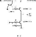
图4是本发明一实施方式的半导体集成电路装置的电路图。4 is a circuit diagram of a semiconductor integrated circuit device according to an embodiment of the present invention.
图5是用于说明本发明一实施方式的半导体集成电路装置的剖面图。5 is a cross-sectional view illustrating a semiconductor integrated circuit device according to an embodiment of the present invention.
图6是用于说明本发明一实施方式的半导体集成电路装置的上表面图。FIG. 6 is a top view illustrating a semiconductor integrated circuit device according to an embodiment of the present invention.
图7(A)与本发明一实施方式的半导体集成电路装置中元件结构有关,是表示功率NPN晶体管的寄生电流值和横向PNP晶体管的基极电流值的关系的曲线图,图7(B)与施加电位有关,是表示功率NPN晶体管的寄生电流值和横向PNP晶体管的基极电流值的关系的曲线图。7(A) is a graph showing the relationship between the parasitic current value of the power NPN transistor and the base current value of the lateral PNP transistor, related to the element structure of the semiconductor integrated circuit device according to the embodiment of the present invention. FIG. 7(B) It is a graph showing the relationship between the parasitic current value of the power NPN transistor and the base current value of the lateral PNP transistor, depending on the applied potential.
具体实施方式Detailed ways
以下,参照图1~图7详细说明本发明的半导体集成电路装置的一实施方式。Hereinafter, an embodiment of the semiconductor integrated circuit device of the present invention will be described in detail with reference to FIGS. 1 to 7 .
图1、图2和图5是表示本发明的半导体集成电路装置的结构的剖面图,图3是形成在本发明的半导体集成电路装置内的二极管结构的剖面图,图4是本发明的半导体集成电路装置中的一部分电路图。再有,在本实施方式中,在半导体集成电路装置中,作为电机的驱动元件,说明功率NPN晶体管的情况,但不限定于这种情况。例如,也可以使用功率MOS晶体管,取代功率NPN晶体管。此外,在图1和图2的剖面图中,图示了横向PNP晶体管元件,而在其他区中,形成NPN晶体管元件等。1, FIG. 2 and FIG. 5 are cross-sectional views showing the structure of the semiconductor integrated circuit device of the present invention, FIG. 3 is a cross-sectional view of a diode structure formed in the semiconductor integrated circuit device of the present invention, and FIG. 4 is a semiconductor integrated circuit device of the present invention. A circuit diagram of a portion of an integrated circuit device. In addition, in this embodiment, a case where a power NPN transistor is used as a driving element of a motor in a semiconductor integrated circuit device is described, but the present invention is not limited to this case. For example, power MOS transistors may also be used instead of power NPN transistors. Furthermore, in the sectional views of FIGS. 1 and 2 , lateral PNP transistor elements are illustrated, while in other regions, NPN transistor elements and the like are formed.
如图1所示,在P型的单晶硅衬底5上,形成厚度2~10μm的N型的外延层6。然后,衬底5和外延层6通过贯通它们的P型的分离区7而形成第一岛区8、第二岛区9和第三岛区10。As shown in FIG. 1 , on a P-type single
这种分离区7由从衬底5表面上下方向扩散的第一分离区11、从外延层6表面形成的第二分离区12构成。然后,通过连结两者,将衬底5和外延层6岛状分离。This
在本实施方式的半导体集成电路装置1中,在第一岛区8中形成横向PNP晶体管2,在第二岛区9中形成二极管3,在第三岛区10中形成功率NPN晶体管4。虽然未图示,但在外延层6上表面中,堆积LOCOS氧化膜、氧化硅膜等。然后,经由形成于氧化硅膜等中的接触孔,堆积阻挡金属层和Al层,形成电极。以下,说明形成于第一岛区8、第二岛区9和第三岛区10中的元件2、3、4。In the semiconductor integrated circuit device 1 of this embodiment, the lateral PNP transistor 2 is formed in the
首先,说明形成于第一岛区8中的功率NPN晶体管2。如图所示,在衬底5和外延层6的边界部分中形成N型的埋入扩散区13。然后,在用作基极区的外延层6中,从其表面起,形成P型的扩散区14、15、16和N型的扩散区17。例如,将P型的扩散区15作为发射极区,将P型的扩散区14、16作为集电极区。再有,在图中,将P型的扩散区14、16独立描绘,但实际上被一体地形成,以便包围发射极区的P型的扩散区15。另一方面,通过将N型的扩散区17用作基极导出区,从而构成功率NPN晶体管2。First, the power NPN transistor 2 formed in the
下面,说明形成于第二岛区9中的二极管3。如图所示,在衬底5和外延层6的边界部分中形成N型的埋入扩散区18。从外延层6的表面形成N型的扩散区19,扩散区19与埋入扩散区18连结。然后,在被N型的扩散区19包围的区中,从外延层6的表面形成P型的扩散区20,在P型的扩散区20中,从其表面形成N型的扩散区21。Next, the diode 3 formed in the second island region 9 will be described. As shown in the figure, an N-type buried diffusion region 18 is formed in the boundary portion between the
在本实施方式中,设P型的扩散区20为阳极区。然后,在外延层6的上表面中,将P型的扩散区20和N型的扩散区21短路,形成阳极电极。由此,可以防止P型的扩散区20和N型的扩散区21的寄生效应。另一方面,将N型的外延层6、N型的扩散区18、19作为阴极区。然后,在外延层6上表面中,形成阴极电极。通过这种结构,形成二极管3。In this embodiment, the P-type diffusion region 20 is assumed to be an anode region. Then, on the upper surface of the
如图所示,在本实施方式中,在形成二极管3时,可以利用形成于半导体集成电路装置1的其他岛区中的元件结构。然后,通过元件上表面的电极、布线结构来形成二极管3。因此,作为二极管3的结构,例如,如图3(A)所示,还可以利用横向PNP晶体管的结构。这种情况下,将P型的扩散区43、44、45作为阳极区,在外延层42上表面中,形成阳极电极。另一方面,将N型的外延层42、N型的扩散区46作为阴极区。然后,在外延层42上表面中,形成阴极电极。As shown in the figure, in this embodiment mode, when forming the diode 3, an element structure formed in another island region of the semiconductor integrated circuit device 1 can be utilized. Then, the diode 3 is formed through the electrode and wiring structure on the upper surface of the element. Therefore, as the structure of the diode 3, for example, a structure of a lateral PNP transistor as shown in FIG. 3(A) can also be used. In this case, the P-
此外,通过图3(B)所示的结构,也可以形成二极管3。这种情况下,将P型的埋入扩散层54、P型的扩散区55作为阳极区。然后,在外延层52上表面中,将P型的扩散区55和N型的扩散区57短路,形成阳极电极。由此,可以防止由P型的扩散区54、55构成的发射极区和N型的扩散区53、56、57构成的基极区及P型的衬底51构成的集电极区所构成的寄生PNP晶体管造成的对衬底51的漏电流。另一方面,将N型的外延层52、N型的扩散区58作为阴极区,在外延层52上表面中,形成阴极电极。In addition, the diode 3 can also be formed with the structure shown in FIG. 3(B). In this case, the P-type buried
下面,说明形成于第三岛区10中的功率NPN晶体管4。如图所示,在衬底5和外延层6的边界部分中形成N型的埋入扩散区22。从外延层6的表面形成N型的扩散区23,扩散区23与埋入扩散区22连结。然后,在被N型的扩散区23包围的区中,从外延层6的表面形成P型的扩散区24。在P型的扩散区24中,从其表面形成N型的扩散区25。然后,在本实施方式中,将N型的外延层6作为集电极区,将N型的埋入扩散区22、扩散区23作为集电极导出区。将P型的扩散区24作为基极区,将N型的扩散区25作为发射极区。Next, the power NPN transistor 4 formed in the
再有,在本实施方式中,为了包围形成作为电机的驱动元件的功率NPN晶体管4的第三岛区10,配置第二岛区9。然后,说明了在第二岛区9中形成二极管元件的情况,但不必限定于这种情况。例如,也可以形成图2所示的结构。如图所示,在第二岛区9中,在衬底5和外延层6的边界部分中形成N型的埋入扩散区26。然后,从外延层6表面形成N型的扩散区27,将两者连结。在N型的扩散区27上施加电源电压。由此,在功率NPN晶体管4中施加电机的反电动势时,从功率NPN晶体管4产生的自由载流子(电子)可从该N型的扩散区26、27吸取。即,在图1和图2的剖面图中,分别表示形成二极管3的情况和被施加电源电压的形成了扩散区26、27的情况。但是,在第二岛区9中,形成两者。Furthermore, in the present embodiment, the second island region 9 is arranged to surround the
这里,在本实施方式中,例如,将流过数mA左右的主电流的情况称为NPN晶体管,例如将流过数A左右的主电流的情况称为功率NPN晶体管。Here, in this embodiment, for example, a case where a main current of about several mA flows is called an NPN transistor, and a case where a main current of about several A flows, for example, is called a power NPN transistor.
其次,如图4所示,本实施方式的半导体集成电路装置1是用于驱动电机的驱动IC,表示该电路图的一部分。例如,在电机驱动的电源线上,连接作为电机驱动元件的功率NPN晶体管A的集电极电极。功率NPN晶体管A的发射极电极和电机的输出端子连接。另一方面,作为控制元件的横向PNP晶体管C的集电极电极和功率NPN晶体管A的基极电极经由电阻R1来连接。然后,横向PNP晶体管C的发射极电极连接到电源线路。基极电极例如与作为电流镜电路形成的另一方的横向PNP晶体管的基极电极连接。然后,经由该横向PNP晶体管连接到电源线。Next, as shown in FIG. 4 , the semiconductor integrated circuit device 1 of the present embodiment is a drive IC for driving a motor, and shows a part of the circuit diagram. For example, the collector electrode of the power NPN transistor A, which is the motor drive element, is connected to the power supply line for the motor drive. The emitter electrode of the power NPN transistor A is connected to the output terminal of the motor. On the other hand, the collector electrode of the lateral PNP transistor C serving as a control element and the base electrode of the power NPN transistor A are connected via a resistor R1. Then, the emitter electrode of the lateral PNP transistor C is connected to the power supply line. The base electrode is connected to the base electrode of the other lateral PNP transistor formed as a current mirror circuit, for example. Then, it is connected to the power supply line via this lateral PNP transistor.
如上述那样,在本实施方式中,在第二岛区9中形成二极管3。然后,将第二岛区9进行配置,以包围形成功率NPN晶体管4的第三岛区10。或者,将第二岛区9配置在第三岛区10的附近区。形成于第二岛区9中的二极管3通过外延层6上表面的布线,其阳极区与形成功率NPN晶体管2的第一岛区8的分离区7电连接。另一方面,二极管3的阴极区通过外延层6上表面的布线,与功率NPN晶体管4的集电极区电连接。As described above, in the present embodiment, the diode 3 is formed in the second island region 9 . Then, the second island region 9 is configured to surround the
根据这种布线结构,例如,在作为驱动元件的功率NPN晶体管4从导通动作向截止动作转移时,从电机产生反电动势,在功率NPN晶体管4上施加该反电动势。由此,在功率NPN晶体管4的集电极区中,施加负的电位,例如-2V左右。另一方面,P型的衬底5经由划分第三岛区10的分离区7被接地。由此,在由功率NPN晶体管4的N型的埋入扩散区22、P型的衬底5、横向PNP晶体管2的N型的埋入扩散区13构成的寄生NPN晶体管中,在发射极区和基极区的结区(以下,称为寄生结区)中施加正向偏置,产生自由载流子(电子)。According to such a wiring structure, for example, when the power NPN transistor 4 serving as a driving element transitions from the on operation to the off operation, a back electromotive force is generated from the motor, and the back electromotive force is applied to the power NPN transistor 4 . As a result, a negative potential, for example, about −2 V, is applied to the collector region of the power NPN transistor 4 . On the other hand, the P-
再有,如上述那样,在本实施方式中,通过电机的反电动势,在功率NPN晶体管4的集电极区中,以施加-2V左右的情况为例,以下进行说明。但是,在功率NPN晶体管4的集电极区中,不限定于施加-2V左右的情况。As described above, in the present embodiment, the case where about -2V is applied to the collector region of the power NPN transistor 4 by the counter electromotive force of the motor will be described below as an example. However, it is not limited to the case where about −2 V is applied to the collector region of the power NPN transistor 4 .
此外,在二极管3中,同样通过电机的反电动势,在二极管3的阳极区中,施加负的电位,例如-2V左右。另一方面,衬底5被接地。由此,在由二极管3的N型的埋入扩散区18、P型的衬底5、横向PNP晶体管2的N型的埋入扩散区13构成的NPN晶体管中,在发射极区和基极区的结区(以下,称为寄生结区)中施加正向偏置,产生自由载流子(电子)。In addition, in the diode 3, a negative potential, such as about -2V, is applied to the anode region of the diode 3 through the back electromotive force of the motor. On the other hand, the
但是,在本实施方式中,通过具有上述的布线结构,二极管3的阳极区为接地状态,而阴极区通过电机的反电动势被施加负的电位,例如施加-2V左右。由此,在二极管3的PN结区中施加正向偏置,二极管3为导通动作,在阳极电极上施加负的电位,例如施加-1.3V左右。而且,在本实施方式中,阳极电极通过布线层与第一岛区8的分离区7电连接。其结果,第一岛区8例如为被施加了-1.3V左右的负电位的分离区7包围的状态。However, in this embodiment, by having the above-mentioned wiring structure, the anode region of the diode 3 is grounded, and the cathode region is given a negative potential, eg, about -2V, by the back electromotive force of the motor. Thus, a forward bias is applied to the PN junction region of the diode 3, the diode 3 is turned on, and a negative potential, for example, about -1.3V is applied to the anode electrode. Furthermore, in the present embodiment, the anode electrode is electrically connected to the
即,在本实施方式中,防止从二极管3和功率NPN晶体管4的寄生结区产生的自由载流子(电子)经由衬底5流入横向PNP晶体管2。如横向PNP晶体管2那样,与其他岛区的分离区7的电位相比,将形成控制驱动元件的小信号类元件的岛区的分离区7的电位降低。由此,从二极管3和功率NPN晶体管4产生的自由载流子(电子)流向被处于接地状态的分离区7包围的其他岛区。而且,在横向PNP晶体管2中,自由载流子(电子)流入基极区,在截止动作时,不进行导通动作。其结果,在本实施方式中,基于作为控制元件的横向PNP晶体管2的寄生效应造成的导通动作,可以防止作为驱动元件的功率NPN晶体管4在截止动作时进行导通动作。That is, in this embodiment, free carriers (electrons) generated from the parasitic junction region of diode 3 and power NPN transistor 4 are prevented from flowing into lateral PNP transistor 2 via
下面,如图5所示,在本实施方式中,例如,即使采用在外延层6上表面中的A1布线,也可以获得与采用上述二极管3的情况同样的效果。Next, as shown in FIG. 5 , in the present embodiment, for example, even if the A1 wiring in the upper surface of the
具体地说,形成横向PNP晶体管2的第一岛区8的分离区7和形成功率NPN晶体管4的第三岛区10的分离区7在外延层6上表面中通过A1布线进行电连接。然后,在功率NPN晶体管4的集电极区中,例如,在作为驱动元件的功率NPN晶体管4从导通动作向截止动作转移时,通过电机的反电动势,被施加负的电位,例如施加-2V左右。在P型的衬底5中,经由划分第三岛区10的分离区7被接地。因此,在由功率NPN晶体管4的P型的衬底5和N型的外延层6及埋入扩散区22构成的寄生结区中施加正向偏置,产生自由载流子(电子)。Specifically, the
由此,在功率NPN晶体管4的寄生结区中施加正向偏置,在划分第三岛区10的分离区7中施加负的电位,例如施加-1.3V左右。而且,在本实施方式中,形成功率NPN晶体管4的第三岛区10的分离区7和形成横向PNP晶体管2的第一岛区8的分离区7通过Al布线进行连接。尽管有Al布线造成的电压降,但通过这种结构,在形成横向PNP晶体管2的第一岛区8的分离区7中,施加-1.0V~-1.3V左右的电压。As a result, a forward bias is applied to the parasitic junction region of the power NPN transistor 4 , and a negative potential, for example, about −1.3 V, is applied to the
即,在形成横向PNP晶体管2的第一岛区8的分离区7中,与处于接地状态的其他岛区的分离区7相比,被施加低的电位。其结果,在第一岛区8中,如上述采用二极管元件3那样,可以防止流入自由载流子(电子)。而且,可以防止寄生效应造成的横向PNP晶体管2的误动作。在本实施方式中,与采用二极管3的情况同样,可以防止作为电机的驱动元件的功率NPN晶体管4的误动作。That is, to the
除此之外,通过期望防止寄生效应造成的误动作的岛区的分离区7通过Al布线与第三岛区10的分离区7电连接,从而防止流入自由载流子(电子)。再有,在本实施方式中,在以包围第三岛区10来配置的第二岛区9内,通过形成施加了电源电位的N型的埋入扩散区26、扩散区27,可以高效率抽取从寄生结区产生的自由载流子(电子)。In addition, the
下面,图6是本发明的半导体集成电路装置1的一部分上表面图,图7是表示本发明的驱动元件中的寄生电流值与控制元件中的基极电流值之间关系的特性图。Next, FIG. 6 is a partial upper surface view of the semiconductor integrated circuit device 1 of the present invention, and FIG. 7 is a characteristic diagram showing the relationship between the parasitic current value in the driving element and the base current value in the control element in the present invention.
如图6所示,在本实施方式中,在半导体芯片61的左侧配置作为电机的驱动元件的功率NPN晶体管用的地线62。在地线62的附近区中,将功率NPN晶体管在Y轴方向上四元件配置。而且,在本实施方式中,如点划线所示,配置分离岛区,以包围功率NPN晶体管。As shown in FIG. 6 , in the present embodiment, a
另一方面,在半导体芯片61的右侧和上下侧中,配置其他元件用的地线63。然后,在地线63的附近区中,配置IIL(Integrated Injection Logic)。然后,在功率NPN晶体管的配置区和IIL的配置区之间,将控制信号传送到功率NPN晶体管的横向PNP晶体管在Y轴方向上四元件配置。如图所示,功率NPN晶体管和横向PNP晶体管通过分离岛区来隔离。On the other hand, on the right side and upper and lower sides of the
在图7(A)中,表示如图6所示那样配置各元件,在Y轴上表示从寄生结区产生自由载流子(电子)情况下的横向PNP晶体管的基极电流值,在X轴上表示流过功率NPN晶体管的寄生电流值。而且,用实线所示的线为现有的结构,不配置二极管,或者表示没有进行金属布线的情况。虚线表示不配置二极管,通过上述的布线连接,将横向PNP晶体管的分离区和功率NPN晶体管的分离区连接的情况。点划线表示在分离岛区中形成二极管,通过上述的布线连接,将二极管和横向PNP晶体管的分离区及功率NPN晶体管的集电极区连接的情况。In FIG. 7(A), each element is arranged as shown in FIG. 6, and the base current value of the lateral PNP transistor in the case where free carriers (electrons) are generated from the parasitic junction region is shown on the Y axis, and the X The value of the parasitic current flowing through the power NPN transistor is indicated on the axis. In addition, the line shown by the solid line is a conventional structure, and a diode is not arrange|positioned, or it shows the case where metal wiring is not performed. The dotted line indicates the case where no diode is arranged, and the separation region of the lateral PNP transistor and the separation region of the power NPN transistor are connected through the above-mentioned wiring connection. The dotted line indicates that a diode is formed in the isolation island region, and the diode is connected to the isolation region of the lateral PNP transistor and the collector region of the power NPN transistor through the above-mentioned wiring connection.
如图所示,在用实线表示的现有结构中,随着对功率NPN晶体管的寄生电流的增大,横向PNP晶体管中的基极电流增大。即,在现有的结构中,随着来自功率NPN晶体管的寄生结区的自由载流子(电子)的产生量的增加,对横向PNP晶体管的基极电流值增加。而且,通过基极电流流过大于或等于一定值,如果本来是横向PNP晶体管的截止动作时,则可能进行导通动作。即,因该横向PNP晶体管的误动作而使功率NPN晶体管也变为导通动作,向电机传送错误的信号,妨碍电机的正常动作。As shown, in the existing structure indicated by the solid line, as the parasitic current to the power NPN transistor increases, the base current in the lateral PNP transistor increases. That is, in the conventional structure, as the amount of free carriers (electrons) generated from the parasitic junction region of the power NPN transistor increases, the value of the base current to the lateral PNP transistor increases. Furthermore, when the base current flows to a value greater than or equal to a certain value, when the lateral PNP transistor is originally in the OFF operation, the ON operation may be performed. That is, due to the malfunction of the lateral PNP transistor, the power NPN transistor is also turned on, and an erroneous signal is transmitted to the motor, thereby preventing normal operation of the motor.
另一方面,在本实施方式中,如虚线和点划线所示,与形成由自由载流子(电子)引起误动作的横向PNP晶体管的岛区有关,形成为在分离区中施加比其他岛区低的电位的结构。由此,随着来自功率NPN晶体管的自由载流子(电子)的增大,可以抑制对横向PNP晶体管中的基极电流值的增大。而且,在横向PNP晶体管中,可以防止自由载流子(电子)造成的误动作。再有,如图所示,与采用二极管元件的情况相比,横向PNP晶体管的分离区比其他分离区的电位低。因此,在横向PNP晶体管中,可以防止自由载流子(电子)造成的基极电流值的增大。On the other hand, in the present embodiment, as shown by the dotted line and the dot-dash line, it is formed to apply a larger than other The structure of the low potential of the island region. Accordingly, it is possible to suppress an increase in the base current value in the lateral PNP transistor as free carriers (electrons) from the power NPN transistor increase. Furthermore, in the lateral PNP transistor, malfunction due to free carriers (electrons) can be prevented. Furthermore, as shown in the figure, the isolation region of the lateral PNP transistor has a lower potential than the other isolation regions compared to the case of using a diode element. Therefore, in the lateral PNP transistor, an increase in the base current value due to free carriers (electrons) can be prevented.
在图7(B)中,表示如图6所示来配置各元件,并表示在改变施加在形成横向PNP晶体管的岛区的分离区上的电位情况下的横向PNP晶体管的基极电流值的变化。再有,在图7(B)中,是将电压直接施加在形成横向PNP晶体管的岛区的分离区情况的数据。此外,在Y轴上,表示从寄生结区产生自由载流子(电子)情况的横向PNP晶体管的基极电流值,在X轴上,表示流过功率NPN晶体管的寄生电流值。In FIG. 7(B), each element is arranged as shown in FIG. 6, and the base current value of the lateral PNP transistor is shown when the potential applied to the separation region forming the island region of the lateral PNP transistor is changed. Variety. In addition, in FIG. 7(B), it is the data of the case where the voltage was directly applied to the isolation|separation area|region which forms the island area|region of the lateral PNP transistor. Also, on the Y axis, the base current value of the lateral PNP transistor when free carriers (electrons) are generated from the parasitic junction region is shown, and on the X axis, the parasitic current value flowing through the power NPN transistor is shown.
如图所示,如用实线所示,在分离区为接地状态(0V)的情况下,被与其他岛区的分离区同电位的分离区包围。因此,随着对功率NPN晶体管的寄生电流的增大,横向PNP晶体管中的基极电流值增大。另一方面,如用虚线所示,在分离区中施加-0.1V的情况下,与其他岛区的分离区相比为低电位。由此,横向PNP晶体管中的基极电流值下降。同样,如用点划线和两点点划线所示,设施加在分离区中的电位为-0.2V、-0.3V。这种情况下,形成横向PNP晶体管的岛区与其他岛区相比,被低电位的分离区包围。由此,横向PNP晶体管中的基极电流值进一步下降。As shown in the figure, as indicated by the solid line, when the separation region is in the ground state (0 V), it is surrounded by separation regions having the same potential as the separation regions of other island regions. Therefore, as the parasitic current to the power NPN transistor increases, the base current value in the lateral PNP transistor increases. On the other hand, when −0.1 V is applied to the separation region, as indicated by the dotted line, the potential is lower than that of the separation regions of other island regions. As a result, the base current value in the lateral PNP transistor decreases. Also, as indicated by the one-dot chain line and the two-dot chain line, the potentials applied by the facility in the separation area are -0.2V, -0.3V. In this case, the island region where the lateral PNP transistor is formed is surrounded by a lower potential isolation region than other island regions. As a result, the base current value in the lateral PNP transistor further decreases.
即,从图7(A)和图7(B)可知,在本实施方式中,在电机产生反电动势时,通过从驱动元件的寄生结区产生的自由载流子(电子),与引起误动作的元件的岛区有关,在分离区中形成与其他岛区相比施加低电位的结构。由此,可以防止通过电机的反电动势,从驱动元件产生的自由载流子(电子)流入形成控制元件的岛区而引起误动作。此时,在本实施方式中,通过二极管和金属布线,可以在要求的分离区中施加比其他分离区低的电位。此外,在形成二极管的分离岛区中,通过形成施加电源电位的N型扩散区,可以吸上自由载流子(电子)。而且,可以有效地防止控制元件的误动作。That is, as can be seen from FIG. 7(A) and FIG. 7(B), in this embodiment, when the motor generates back electromotive force, free carriers (electrons) generated from the parasitic junction region of the drive element are used to cause errors. Regarding the island region of the operating element, a structure is formed in which a lower potential is applied to the isolation region than other island regions. This prevents free carriers (electrons) generated from the driving element from flowing into the island forming the control element due to the counter electromotive force of the motor and causing malfunction. At this time, in this embodiment mode, a potential lower than that of other isolation regions can be applied to a desired isolation region by means of the diode and the metal wiring. In addition, in the isolated island region where the diode is formed, free carriers (electrons) can be absorbed by forming an N-type diffusion region to which a power supply potential is applied. Furthermore, malfunction of the control element can be effectively prevented.
再有,在本实施方式中,说明了将二极管装入同一衬底构成的半导体集成电路装置内的情况,但不限定于这种情况。例如,准备单独形成的二极管,即使进行外部连接,也可获得同样的效果。此外,也可以置换为形成受到寄生效应影响的元件的岛区的分离区的电位与其他岛区的分离区的电位相比可为低电位的任意的结构。另外,在不脱离本发明的要点的范围内,可进行各种变更。In addition, in this embodiment mode, the case where the diode is incorporated in the semiconductor integrated circuit device constituted by the same substrate has been described, but it is not limited to this case. For example, even if a diode formed separately is prepared and connected externally, the same effect can be obtained. In addition, it may be replaced with any structure in which the potential of the isolation region of the island region forming the element affected by the parasitic effect is lower than the potential of the isolation region of the other island regions. In addition, various changes can be made without departing from the gist of the present invention.
Claims (7)
Translated fromChineseApplications Claiming Priority (3)
| Application Number | Priority Date | Filing Date | Title |
|---|---|---|---|
| JP338865/03 | 2003-09-29 | ||
| JP338865/2003 | 2003-09-29 | ||
| JP2003338865AJP4775682B2 (en) | 2003-09-29 | 2003-09-29 | Semiconductor integrated circuit device |
Publications (2)
| Publication Number | Publication Date |
|---|---|
| CN1604328A CN1604328A (en) | 2005-04-06 |
| CN1324709Ctrue CN1324709C (en) | 2007-07-04 |
Family
ID=34509664
Family Applications (1)
| Application Number | Title | Priority Date | Filing Date |
|---|---|---|---|
| CNB2004100825250AExpired - Fee RelatedCN1324709C (en) | 2003-09-29 | 2004-09-20 | Semiconductor integrated circuit device |
Country Status (4)
| Country | Link |
|---|---|
| US (1) | US7381998B2 (en) |
| JP (1) | JP4775682B2 (en) |
| CN (1) | CN1324709C (en) |
| TW (1) | TWI244751B (en) |
Families Citing this family (6)
| Publication number | Priority date | Publication date | Assignee | Title |
|---|---|---|---|---|
| CN100414685C (en)* | 2006-08-28 | 2008-08-27 | 汤庆敏 | Manufacturing process of semiconductor device chip punch through isolation area and PN junction |
| CN102623453B (en)* | 2011-01-27 | 2014-10-29 | 无锡华润华晶微电子有限公司 | Power device, preparation method and energy-saving electronic lighting circuit using the same |
| JP6132539B2 (en)* | 2012-12-13 | 2017-05-24 | ルネサスエレクトロニクス株式会社 | Semiconductor device |
| US9806148B2 (en)* | 2015-04-07 | 2017-10-31 | Texas Instruments Incorporated | Device isolator with reduced parasitic capacitance |
| JP6679908B2 (en)* | 2015-12-11 | 2020-04-15 | セイコーエプソン株式会社 | Semiconductor device and manufacturing method thereof |
| JP7422547B2 (en)* | 2020-01-15 | 2024-01-26 | ローム株式会社 | semiconductor equipment |
Citations (2)
| Publication number | Priority date | Publication date | Assignee | Title |
|---|---|---|---|---|
| JPH08213552A (en)* | 1995-01-31 | 1996-08-20 | Sanyo Electric Co Ltd | Semiconductor integrated circuit |
| CN1365151A (en)* | 2000-12-25 | 2002-08-21 | 三洋电机株式会社 | Semiconductor integrated circuit device and its producing method |
Family Cites Families (13)
| Publication number | Priority date | Publication date | Assignee | Title |
|---|---|---|---|---|
| IT1197279B (en)* | 1986-09-25 | 1988-11-30 | Sgs Microelettronica Spa | INTEGRATED DEVICE TO SCREEN THE INJECTION OF CHARGES INTO THE SUBSTRATE, IN PARTICULAR IN PILOTING CIRCUITS OF INDUCTIVE AND / OR CAPACITIVE LOADS |
| JPH0220056A (en)* | 1988-07-07 | 1990-01-23 | Toshiba Corp | semiconductor equipment |
| JP2629028B2 (en)* | 1988-08-10 | 1997-07-09 | 株式会社日立製作所 | Clock signal supply method and device |
| JP2725359B2 (en)* | 1989-03-27 | 1998-03-11 | 日本電気株式会社 | Semiconductor integrated circuit device |
| EP0442064B1 (en)* | 1990-02-15 | 1996-03-27 | Siemens Aktiengesellschaft | Input protection structure for integrated circuits |
| JPH04329665A (en)* | 1991-05-01 | 1992-11-18 | Matsushita Electron Corp | Driving semiconductor integrated circuit device |
| JPH06104459A (en) | 1992-09-21 | 1994-04-15 | Sanken Electric Co Ltd | Semiconductor device |
| JP3139313B2 (en)* | 1993-12-27 | 2001-02-26 | 株式会社デンソー | Bipolar semiconductor integrated circuit |
| JP3271738B2 (en)* | 1995-12-27 | 2002-04-08 | 株式会社沖データ | Data transfer device |
| DE69629278D1 (en)* | 1996-04-30 | 2003-09-04 | St Microelectronics Srl | Circuit for the controlled, vibration-free return of the discharge current of an inductive load |
| JP3917689B2 (en)* | 1996-08-19 | 2007-05-23 | 新電元工業株式会社 | Semiconductor device |
| JP2000138229A (en)* | 1998-11-04 | 2000-05-16 | Rohm Co Ltd | Semiconductor device |
| US7002687B2 (en)* | 2001-12-27 | 2006-02-21 | Taiwan Unison Biotechnology Co., Ltd. | Quantitative scanning analyzer unit |
- 2003
- 2003-09-29JPJP2003338865Apatent/JP4775682B2/ennot_activeExpired - Fee Related
- 2004
- 2004-08-26TWTW093125460Apatent/TWI244751B/ennot_activeIP Right Cessation
- 2004-09-20CNCNB2004100825250Apatent/CN1324709C/ennot_activeExpired - Fee Related
- 2004-09-24USUS10/949,569patent/US7381998B2/ennot_activeExpired - Lifetime
Patent Citations (2)
| Publication number | Priority date | Publication date | Assignee | Title |
|---|---|---|---|---|
| JPH08213552A (en)* | 1995-01-31 | 1996-08-20 | Sanyo Electric Co Ltd | Semiconductor integrated circuit |
| CN1365151A (en)* | 2000-12-25 | 2002-08-21 | 三洋电机株式会社 | Semiconductor integrated circuit device and its producing method |
Also Published As
| Publication number | Publication date |
|---|---|
| US20050087771A1 (en) | 2005-04-28 |
| JP4775682B2 (en) | 2011-09-21 |
| TWI244751B (en) | 2005-12-01 |
| CN1604328A (en) | 2005-04-06 |
| JP2005109050A (en) | 2005-04-21 |
| TW200512928A (en) | 2005-04-01 |
| US7381998B2 (en) | 2008-06-03 |
Similar Documents
| Publication | Publication Date | Title |
|---|---|---|
| CN1305138C (en) | Semiconductor integrated circuit device | |
| CN1201404C (en) | Semiconductor device for substrate triggered electrostatic discharge protection | |
| CN1203553C (en) | Low voltage trigger silicon controlled rectifier with silicon insulating layer and electrostatic discharge protection circuit | |
| CN1630078A (en) | Semiconductor device | |
| CN1828898A (en) | Semiconductor device | |
| CN109428535B (en) | Motor drive circuits, semiconductor devices, and electronic equipment | |
| CN101361193B (en) | Floating gate structure with high electrostatic discharge performance | |
| CN108630681B (en) | Semiconductor integrated circuit device | |
| CN1196206C (en) | Light-emitting thyristor matrix array and driver circuit | |
| CN1324709C (en) | Semiconductor integrated circuit device | |
| CN1581354A (en) | Semiconductor device | |
| CN1914731A (en) | Buffer circuit having electrostatic discharge protection | |
| CN1127142C (en) | Semiconductor device | |
| JP2004247400A (en) | Semiconductor device | |
| CN1136611C (en) | Semiconductor device with a plurality of transistors | |
| CN1604327A (en) | semiconductor integrated circuit device | |
| CN1941370A (en) | Static Protection System | |
| CN1237615C (en) | A diode structure and its electrostatic discharge protection circuit | |
| CN1241262C (en) | Static discharge protection circuit and relative metal oxide semiconductor transistor structure | |
| CN1873983A (en) | Semiconductor integrated circuit device | |
| JP2012243930A (en) | Semiconductor device, semiconductor package and semiconductor device manufacturing method | |
| CN1448911A (en) | Input and output protection circuit of liquid crystal display device | |
| CN1217577A (en) | Semiconductor device, electrostatic discharge protection element and method for preventing insulation breakdown | |
| CN1236188A (en) | Semiconductor device | |
| JP4671666B2 (en) | Driving circuit |
Legal Events
| Date | Code | Title | Description |
|---|---|---|---|
| C06 | Publication | ||
| PB01 | Publication | ||
| C10 | Entry into substantive examination | ||
| SE01 | Entry into force of request for substantive examination | ||
| C14 | Grant of patent or utility model | ||
| GR01 | Patent grant | ||
| CF01 | Termination of patent right due to non-payment of annual fee | ||
| CF01 | Termination of patent right due to non-payment of annual fee | Granted publication date:20070704 Termination date:20200920 |