CN1314715A - Semiconductor device and manufacturing method thereof - Google Patents
Semiconductor device and manufacturing method thereofDownload PDFInfo
- Publication number
- CN1314715A CN1314715ACN01117390ACN01117390ACN1314715ACN 1314715 ACN1314715 ACN 1314715ACN 01117390 ACN01117390 ACN 01117390ACN 01117390 ACN01117390 ACN 01117390ACN 1314715 ACN1314715 ACN 1314715A
- Authority
- CN
- China
- Prior art keywords
- insulating film
- electrode
- semiconductor device
- semiconductor layer
- pixel
- Prior art date
- Legal status (The legal status is an assumption and is not a legal conclusion. Google has not performed a legal analysis and makes no representation as to the accuracy of the status listed.)
- Granted
Links
Images


Classifications
- G—PHYSICS
- G02—OPTICS
- G02F—OPTICAL DEVICES OR ARRANGEMENTS FOR THE CONTROL OF LIGHT BY MODIFICATION OF THE OPTICAL PROPERTIES OF THE MEDIA OF THE ELEMENTS INVOLVED THEREIN; NON-LINEAR OPTICS; FREQUENCY-CHANGING OF LIGHT; OPTICAL LOGIC ELEMENTS; OPTICAL ANALOGUE/DIGITAL CONVERTERS
- G02F1/00—Devices or arrangements for the control of the intensity, colour, phase, polarisation or direction of light arriving from an independent light source, e.g. switching, gating or modulating; Non-linear optics
- G02F1/01—Devices or arrangements for the control of the intensity, colour, phase, polarisation or direction of light arriving from an independent light source, e.g. switching, gating or modulating; Non-linear optics for the control of the intensity, phase, polarisation or colour
- G02F1/13—Devices or arrangements for the control of the intensity, colour, phase, polarisation or direction of light arriving from an independent light source, e.g. switching, gating or modulating; Non-linear optics for the control of the intensity, phase, polarisation or colour based on liquid crystals, e.g. single liquid crystal display cells
- G02F1/133—Constructional arrangements; Operation of liquid crystal cells; Circuit arrangements
- G02F1/136—Liquid crystal cells structurally associated with a semi-conducting layer or substrate, e.g. cells forming part of an integrated circuit
- H—ELECTRICITY
- H10—SEMICONDUCTOR DEVICES; ELECTRIC SOLID-STATE DEVICES NOT OTHERWISE PROVIDED FOR
- H10D—INORGANIC ELECTRIC SEMICONDUCTOR DEVICES
- H10D30/00—Field-effect transistors [FET]
- H10D30/60—Insulated-gate field-effect transistors [IGFET]
- H10D30/67—Thin-film transistors [TFT]
- G—PHYSICS
- G02—OPTICS
- G02F—OPTICAL DEVICES OR ARRANGEMENTS FOR THE CONTROL OF LIGHT BY MODIFICATION OF THE OPTICAL PROPERTIES OF THE MEDIA OF THE ELEMENTS INVOLVED THEREIN; NON-LINEAR OPTICS; FREQUENCY-CHANGING OF LIGHT; OPTICAL LOGIC ELEMENTS; OPTICAL ANALOGUE/DIGITAL CONVERTERS
- G02F1/00—Devices or arrangements for the control of the intensity, colour, phase, polarisation or direction of light arriving from an independent light source, e.g. switching, gating or modulating; Non-linear optics
- G02F1/01—Devices or arrangements for the control of the intensity, colour, phase, polarisation or direction of light arriving from an independent light source, e.g. switching, gating or modulating; Non-linear optics for the control of the intensity, phase, polarisation or colour
- G02F1/13—Devices or arrangements for the control of the intensity, colour, phase, polarisation or direction of light arriving from an independent light source, e.g. switching, gating or modulating; Non-linear optics for the control of the intensity, phase, polarisation or colour based on liquid crystals, e.g. single liquid crystal display cells
- G02F1/133—Constructional arrangements; Operation of liquid crystal cells; Circuit arrangements
- G02F1/1333—Constructional arrangements; Manufacturing methods
- G02F1/133345—Insulating layers
- G—PHYSICS
- G02—OPTICS
- G02F—OPTICAL DEVICES OR ARRANGEMENTS FOR THE CONTROL OF LIGHT BY MODIFICATION OF THE OPTICAL PROPERTIES OF THE MEDIA OF THE ELEMENTS INVOLVED THEREIN; NON-LINEAR OPTICS; FREQUENCY-CHANGING OF LIGHT; OPTICAL LOGIC ELEMENTS; OPTICAL ANALOGUE/DIGITAL CONVERTERS
- G02F1/00—Devices or arrangements for the control of the intensity, colour, phase, polarisation or direction of light arriving from an independent light source, e.g. switching, gating or modulating; Non-linear optics
- G02F1/01—Devices or arrangements for the control of the intensity, colour, phase, polarisation or direction of light arriving from an independent light source, e.g. switching, gating or modulating; Non-linear optics for the control of the intensity, phase, polarisation or colour
- G02F1/13—Devices or arrangements for the control of the intensity, colour, phase, polarisation or direction of light arriving from an independent light source, e.g. switching, gating or modulating; Non-linear optics for the control of the intensity, phase, polarisation or colour based on liquid crystals, e.g. single liquid crystal display cells
- G02F1/133—Constructional arrangements; Operation of liquid crystal cells; Circuit arrangements
- G02F1/1333—Constructional arrangements; Manufacturing methods
- G02F1/1335—Structural association of cells with optical devices, e.g. polarisers or reflectors
- G02F1/133509—Filters, e.g. light shielding masks
- G02F1/133512—Light shielding layers, e.g. black matrix
- G—PHYSICS
- G02—OPTICS
- G02F—OPTICAL DEVICES OR ARRANGEMENTS FOR THE CONTROL OF LIGHT BY MODIFICATION OF THE OPTICAL PROPERTIES OF THE MEDIA OF THE ELEMENTS INVOLVED THEREIN; NON-LINEAR OPTICS; FREQUENCY-CHANGING OF LIGHT; OPTICAL LOGIC ELEMENTS; OPTICAL ANALOGUE/DIGITAL CONVERTERS
- G02F1/00—Devices or arrangements for the control of the intensity, colour, phase, polarisation or direction of light arriving from an independent light source, e.g. switching, gating or modulating; Non-linear optics
- G02F1/01—Devices or arrangements for the control of the intensity, colour, phase, polarisation or direction of light arriving from an independent light source, e.g. switching, gating or modulating; Non-linear optics for the control of the intensity, phase, polarisation or colour
- G02F1/13—Devices or arrangements for the control of the intensity, colour, phase, polarisation or direction of light arriving from an independent light source, e.g. switching, gating or modulating; Non-linear optics for the control of the intensity, phase, polarisation or colour based on liquid crystals, e.g. single liquid crystal display cells
- G02F1/133—Constructional arrangements; Operation of liquid crystal cells; Circuit arrangements
- G02F1/1333—Constructional arrangements; Manufacturing methods
- G02F1/1335—Structural association of cells with optical devices, e.g. polarisers or reflectors
- G02F1/133509—Filters, e.g. light shielding masks
- G02F1/133514—Colour filters
- G—PHYSICS
- G02—OPTICS
- G02F—OPTICAL DEVICES OR ARRANGEMENTS FOR THE CONTROL OF LIGHT BY MODIFICATION OF THE OPTICAL PROPERTIES OF THE MEDIA OF THE ELEMENTS INVOLVED THEREIN; NON-LINEAR OPTICS; FREQUENCY-CHANGING OF LIGHT; OPTICAL LOGIC ELEMENTS; OPTICAL ANALOGUE/DIGITAL CONVERTERS
- G02F1/00—Devices or arrangements for the control of the intensity, colour, phase, polarisation or direction of light arriving from an independent light source, e.g. switching, gating or modulating; Non-linear optics
- G02F1/01—Devices or arrangements for the control of the intensity, colour, phase, polarisation or direction of light arriving from an independent light source, e.g. switching, gating or modulating; Non-linear optics for the control of the intensity, phase, polarisation or colour
- G02F1/13—Devices or arrangements for the control of the intensity, colour, phase, polarisation or direction of light arriving from an independent light source, e.g. switching, gating or modulating; Non-linear optics for the control of the intensity, phase, polarisation or colour based on liquid crystals, e.g. single liquid crystal display cells
- G02F1/133—Constructional arrangements; Operation of liquid crystal cells; Circuit arrangements
- G02F1/1333—Constructional arrangements; Manufacturing methods
- G02F1/1337—Surface-induced orientation of the liquid crystal molecules, e.g. by alignment layers
- G02F1/13378—Surface-induced orientation of the liquid crystal molecules, e.g. by alignment layers by treatment of the surface, e.g. embossing, rubbing or light irradiation
- G02F1/133784—Surface-induced orientation of the liquid crystal molecules, e.g. by alignment layers by treatment of the surface, e.g. embossing, rubbing or light irradiation by rubbing
- G—PHYSICS
- G02—OPTICS
- G02F—OPTICAL DEVICES OR ARRANGEMENTS FOR THE CONTROL OF LIGHT BY MODIFICATION OF THE OPTICAL PROPERTIES OF THE MEDIA OF THE ELEMENTS INVOLVED THEREIN; NON-LINEAR OPTICS; FREQUENCY-CHANGING OF LIGHT; OPTICAL LOGIC ELEMENTS; OPTICAL ANALOGUE/DIGITAL CONVERTERS
- G02F1/00—Devices or arrangements for the control of the intensity, colour, phase, polarisation or direction of light arriving from an independent light source, e.g. switching, gating or modulating; Non-linear optics
- G02F1/01—Devices or arrangements for the control of the intensity, colour, phase, polarisation or direction of light arriving from an independent light source, e.g. switching, gating or modulating; Non-linear optics for the control of the intensity, phase, polarisation or colour
- G02F1/13—Devices or arrangements for the control of the intensity, colour, phase, polarisation or direction of light arriving from an independent light source, e.g. switching, gating or modulating; Non-linear optics for the control of the intensity, phase, polarisation or colour based on liquid crystals, e.g. single liquid crystal display cells
- G02F1/133—Constructional arrangements; Operation of liquid crystal cells; Circuit arrangements
- G02F1/1333—Constructional arrangements; Manufacturing methods
- G02F1/1339—Gaskets; Spacers; Sealing of cells
- G02F1/13394—Gaskets; Spacers; Sealing of cells spacers regularly patterned on the cell subtrate, e.g. walls, pillars
- G—PHYSICS
- G02—OPTICS
- G02F—OPTICAL DEVICES OR ARRANGEMENTS FOR THE CONTROL OF LIGHT BY MODIFICATION OF THE OPTICAL PROPERTIES OF THE MEDIA OF THE ELEMENTS INVOLVED THEREIN; NON-LINEAR OPTICS; FREQUENCY-CHANGING OF LIGHT; OPTICAL LOGIC ELEMENTS; OPTICAL ANALOGUE/DIGITAL CONVERTERS
- G02F1/00—Devices or arrangements for the control of the intensity, colour, phase, polarisation or direction of light arriving from an independent light source, e.g. switching, gating or modulating; Non-linear optics
- G02F1/01—Devices or arrangements for the control of the intensity, colour, phase, polarisation or direction of light arriving from an independent light source, e.g. switching, gating or modulating; Non-linear optics for the control of the intensity, phase, polarisation or colour
- G02F1/13—Devices or arrangements for the control of the intensity, colour, phase, polarisation or direction of light arriving from an independent light source, e.g. switching, gating or modulating; Non-linear optics for the control of the intensity, phase, polarisation or colour based on liquid crystals, e.g. single liquid crystal display cells
- G02F1/133—Constructional arrangements; Operation of liquid crystal cells; Circuit arrangements
- G02F1/1333—Constructional arrangements; Manufacturing methods
- G02F1/1343—Electrodes
- G02F1/134309—Electrodes characterised by their geometrical arrangement
- G02F1/134336—Matrix
- G—PHYSICS
- G02—OPTICS
- G02F—OPTICAL DEVICES OR ARRANGEMENTS FOR THE CONTROL OF LIGHT BY MODIFICATION OF THE OPTICAL PROPERTIES OF THE MEDIA OF THE ELEMENTS INVOLVED THEREIN; NON-LINEAR OPTICS; FREQUENCY-CHANGING OF LIGHT; OPTICAL LOGIC ELEMENTS; OPTICAL ANALOGUE/DIGITAL CONVERTERS
- G02F1/00—Devices or arrangements for the control of the intensity, colour, phase, polarisation or direction of light arriving from an independent light source, e.g. switching, gating or modulating; Non-linear optics
- G02F1/01—Devices or arrangements for the control of the intensity, colour, phase, polarisation or direction of light arriving from an independent light source, e.g. switching, gating or modulating; Non-linear optics for the control of the intensity, phase, polarisation or colour
- G02F1/13—Devices or arrangements for the control of the intensity, colour, phase, polarisation or direction of light arriving from an independent light source, e.g. switching, gating or modulating; Non-linear optics for the control of the intensity, phase, polarisation or colour based on liquid crystals, e.g. single liquid crystal display cells
- G02F1/133—Constructional arrangements; Operation of liquid crystal cells; Circuit arrangements
- G02F1/1333—Constructional arrangements; Manufacturing methods
- G02F1/1343—Electrodes
- G02F1/134309—Electrodes characterised by their geometrical arrangement
- G02F1/134363—Electrodes characterised by their geometrical arrangement for applying an electric field parallel to the substrate, i.e. in-plane switching [IPS]
- G—PHYSICS
- G02—OPTICS
- G02F—OPTICAL DEVICES OR ARRANGEMENTS FOR THE CONTROL OF LIGHT BY MODIFICATION OF THE OPTICAL PROPERTIES OF THE MEDIA OF THE ELEMENTS INVOLVED THEREIN; NON-LINEAR OPTICS; FREQUENCY-CHANGING OF LIGHT; OPTICAL LOGIC ELEMENTS; OPTICAL ANALOGUE/DIGITAL CONVERTERS
- G02F1/00—Devices or arrangements for the control of the intensity, colour, phase, polarisation or direction of light arriving from an independent light source, e.g. switching, gating or modulating; Non-linear optics
- G02F1/01—Devices or arrangements for the control of the intensity, colour, phase, polarisation or direction of light arriving from an independent light source, e.g. switching, gating or modulating; Non-linear optics for the control of the intensity, phase, polarisation or colour
- G02F1/13—Devices or arrangements for the control of the intensity, colour, phase, polarisation or direction of light arriving from an independent light source, e.g. switching, gating or modulating; Non-linear optics for the control of the intensity, phase, polarisation or colour based on liquid crystals, e.g. single liquid crystal display cells
- G02F1/133—Constructional arrangements; Operation of liquid crystal cells; Circuit arrangements
- G02F1/1333—Constructional arrangements; Manufacturing methods
- G02F1/1343—Electrodes
- G02F1/13439—Electrodes characterised by their electrical, optical, physical properties; materials therefor; method of making
- G—PHYSICS
- G02—OPTICS
- G02F—OPTICAL DEVICES OR ARRANGEMENTS FOR THE CONTROL OF LIGHT BY MODIFICATION OF THE OPTICAL PROPERTIES OF THE MEDIA OF THE ELEMENTS INVOLVED THEREIN; NON-LINEAR OPTICS; FREQUENCY-CHANGING OF LIGHT; OPTICAL LOGIC ELEMENTS; OPTICAL ANALOGUE/DIGITAL CONVERTERS
- G02F1/00—Devices or arrangements for the control of the intensity, colour, phase, polarisation or direction of light arriving from an independent light source, e.g. switching, gating or modulating; Non-linear optics
- G02F1/01—Devices or arrangements for the control of the intensity, colour, phase, polarisation or direction of light arriving from an independent light source, e.g. switching, gating or modulating; Non-linear optics for the control of the intensity, phase, polarisation or colour
- G02F1/13—Devices or arrangements for the control of the intensity, colour, phase, polarisation or direction of light arriving from an independent light source, e.g. switching, gating or modulating; Non-linear optics for the control of the intensity, phase, polarisation or colour based on liquid crystals, e.g. single liquid crystal display cells
- G02F1/133—Constructional arrangements; Operation of liquid crystal cells; Circuit arrangements
- G02F1/1333—Constructional arrangements; Manufacturing methods
- G02F1/1345—Conductors connecting electrodes to cell terminals
- G02F1/13454—Drivers integrated on the active matrix substrate
- G—PHYSICS
- G02—OPTICS
- G02F—OPTICAL DEVICES OR ARRANGEMENTS FOR THE CONTROL OF LIGHT BY MODIFICATION OF THE OPTICAL PROPERTIES OF THE MEDIA OF THE ELEMENTS INVOLVED THEREIN; NON-LINEAR OPTICS; FREQUENCY-CHANGING OF LIGHT; OPTICAL LOGIC ELEMENTS; OPTICAL ANALOGUE/DIGITAL CONVERTERS
- G02F1/00—Devices or arrangements for the control of the intensity, colour, phase, polarisation or direction of light arriving from an independent light source, e.g. switching, gating or modulating; Non-linear optics
- G02F1/01—Devices or arrangements for the control of the intensity, colour, phase, polarisation or direction of light arriving from an independent light source, e.g. switching, gating or modulating; Non-linear optics for the control of the intensity, phase, polarisation or colour
- G02F1/13—Devices or arrangements for the control of the intensity, colour, phase, polarisation or direction of light arriving from an independent light source, e.g. switching, gating or modulating; Non-linear optics for the control of the intensity, phase, polarisation or colour based on liquid crystals, e.g. single liquid crystal display cells
- G02F1/133—Constructional arrangements; Operation of liquid crystal cells; Circuit arrangements
- G02F1/136—Liquid crystal cells structurally associated with a semi-conducting layer or substrate, e.g. cells forming part of an integrated circuit
- G02F1/1362—Active matrix addressed cells
- G02F1/136213—Storage capacitors associated with the pixel electrode
- G—PHYSICS
- G02—OPTICS
- G02F—OPTICAL DEVICES OR ARRANGEMENTS FOR THE CONTROL OF LIGHT BY MODIFICATION OF THE OPTICAL PROPERTIES OF THE MEDIA OF THE ELEMENTS INVOLVED THEREIN; NON-LINEAR OPTICS; FREQUENCY-CHANGING OF LIGHT; OPTICAL LOGIC ELEMENTS; OPTICAL ANALOGUE/DIGITAL CONVERTERS
- G02F1/00—Devices or arrangements for the control of the intensity, colour, phase, polarisation or direction of light arriving from an independent light source, e.g. switching, gating or modulating; Non-linear optics
- G02F1/01—Devices or arrangements for the control of the intensity, colour, phase, polarisation or direction of light arriving from an independent light source, e.g. switching, gating or modulating; Non-linear optics for the control of the intensity, phase, polarisation or colour
- G02F1/13—Devices or arrangements for the control of the intensity, colour, phase, polarisation or direction of light arriving from an independent light source, e.g. switching, gating or modulating; Non-linear optics for the control of the intensity, phase, polarisation or colour based on liquid crystals, e.g. single liquid crystal display cells
- G02F1/133—Constructional arrangements; Operation of liquid crystal cells; Circuit arrangements
- G02F1/136—Liquid crystal cells structurally associated with a semi-conducting layer or substrate, e.g. cells forming part of an integrated circuit
- G02F1/1362—Active matrix addressed cells
- G02F1/136227—Through-hole connection of the pixel electrode to the active element through an insulation layer
- G—PHYSICS
- G02—OPTICS
- G02F—OPTICAL DEVICES OR ARRANGEMENTS FOR THE CONTROL OF LIGHT BY MODIFICATION OF THE OPTICAL PROPERTIES OF THE MEDIA OF THE ELEMENTS INVOLVED THEREIN; NON-LINEAR OPTICS; FREQUENCY-CHANGING OF LIGHT; OPTICAL LOGIC ELEMENTS; OPTICAL ANALOGUE/DIGITAL CONVERTERS
- G02F1/00—Devices or arrangements for the control of the intensity, colour, phase, polarisation or direction of light arriving from an independent light source, e.g. switching, gating or modulating; Non-linear optics
- G02F1/01—Devices or arrangements for the control of the intensity, colour, phase, polarisation or direction of light arriving from an independent light source, e.g. switching, gating or modulating; Non-linear optics for the control of the intensity, phase, polarisation or colour
- G02F1/13—Devices or arrangements for the control of the intensity, colour, phase, polarisation or direction of light arriving from an independent light source, e.g. switching, gating or modulating; Non-linear optics for the control of the intensity, phase, polarisation or colour based on liquid crystals, e.g. single liquid crystal display cells
- G02F1/133—Constructional arrangements; Operation of liquid crystal cells; Circuit arrangements
- G02F1/136—Liquid crystal cells structurally associated with a semi-conducting layer or substrate, e.g. cells forming part of an integrated circuit
- G02F1/1362—Active matrix addressed cells
- G02F1/136286—Wiring, e.g. gate line, drain line
- G—PHYSICS
- G02—OPTICS
- G02F—OPTICAL DEVICES OR ARRANGEMENTS FOR THE CONTROL OF LIGHT BY MODIFICATION OF THE OPTICAL PROPERTIES OF THE MEDIA OF THE ELEMENTS INVOLVED THEREIN; NON-LINEAR OPTICS; FREQUENCY-CHANGING OF LIGHT; OPTICAL LOGIC ELEMENTS; OPTICAL ANALOGUE/DIGITAL CONVERTERS
- G02F1/00—Devices or arrangements for the control of the intensity, colour, phase, polarisation or direction of light arriving from an independent light source, e.g. switching, gating or modulating; Non-linear optics
- G02F1/01—Devices or arrangements for the control of the intensity, colour, phase, polarisation or direction of light arriving from an independent light source, e.g. switching, gating or modulating; Non-linear optics for the control of the intensity, phase, polarisation or colour
- G02F1/13—Devices or arrangements for the control of the intensity, colour, phase, polarisation or direction of light arriving from an independent light source, e.g. switching, gating or modulating; Non-linear optics for the control of the intensity, phase, polarisation or colour based on liquid crystals, e.g. single liquid crystal display cells
- G02F1/133—Constructional arrangements; Operation of liquid crystal cells; Circuit arrangements
- G02F1/136—Liquid crystal cells structurally associated with a semi-conducting layer or substrate, e.g. cells forming part of an integrated circuit
- G02F1/1362—Active matrix addressed cells
- G02F1/1368—Active matrix addressed cells in which the switching element is a three-electrode device
- H—ELECTRICITY
- H01—ELECTRIC ELEMENTS
- H01L—SEMICONDUCTOR DEVICES NOT COVERED BY CLASS H10
- H01L21/00—Processes or apparatus adapted for the manufacture or treatment of semiconductor or solid state devices or of parts thereof
- H01L21/02—Manufacture or treatment of semiconductor devices or of parts thereof
- H01L21/02104—Forming layers
- H01L21/02365—Forming inorganic semiconducting materials on a substrate
- H01L21/02656—Special treatments
- H01L21/02664—Aftertreatments
- H01L21/02667—Crystallisation or recrystallisation of non-monocrystalline semiconductor materials, e.g. regrowth
- H01L21/02675—Crystallisation or recrystallisation of non-monocrystalline semiconductor materials, e.g. regrowth using laser beams
- H—ELECTRICITY
- H10—SEMICONDUCTOR DEVICES; ELECTRIC SOLID-STATE DEVICES NOT OTHERWISE PROVIDED FOR
- H10D—INORGANIC ELECTRIC SEMICONDUCTOR DEVICES
- H10D30/00—Field-effect transistors [FET]
- H10D30/60—Insulated-gate field-effect transistors [IGFET]
- H10D30/67—Thin-film transistors [TFT]
- H10D30/6704—Thin-film transistors [TFT] having supplementary regions or layers in the thin films or in the insulated bulk substrates for controlling properties of the device
- H10D30/6713—Thin-film transistors [TFT] having supplementary regions or layers in the thin films or in the insulated bulk substrates for controlling properties of the device characterised by the properties of the source or drain regions, e.g. compositions or sectional shapes
- H10D30/6715—Thin-film transistors [TFT] having supplementary regions or layers in the thin films or in the insulated bulk substrates for controlling properties of the device characterised by the properties of the source or drain regions, e.g. compositions or sectional shapes characterised by the doping profiles, e.g. having lightly-doped source or drain extensions
- H10D30/6719—Thin-film transistors [TFT] having supplementary regions or layers in the thin films or in the insulated bulk substrates for controlling properties of the device characterised by the properties of the source or drain regions, e.g. compositions or sectional shapes characterised by the doping profiles, e.g. having lightly-doped source or drain extensions having significant overlap between the lightly-doped drains and the gate electrodes, e.g. gate-overlapped LDD [GOLDD] TFTs
- H—ELECTRICITY
- H10—SEMICONDUCTOR DEVICES; ELECTRIC SOLID-STATE DEVICES NOT OTHERWISE PROVIDED FOR
- H10D—INORGANIC ELECTRIC SEMICONDUCTOR DEVICES
- H10D30/00—Field-effect transistors [FET]
- H10D30/60—Insulated-gate field-effect transistors [IGFET]
- H10D30/67—Thin-film transistors [TFT]
- H10D30/6729—Thin-film transistors [TFT] characterised by the electrodes
- H10D30/673—Thin-film transistors [TFT] characterised by the electrodes characterised by the shapes, relative sizes or dispositions of the gate electrodes
- H10D30/6731—Top-gate only TFTs
- H—ELECTRICITY
- H10—SEMICONDUCTOR DEVICES; ELECTRIC SOLID-STATE DEVICES NOT OTHERWISE PROVIDED FOR
- H10D—INORGANIC ELECTRIC SEMICONDUCTOR DEVICES
- H10D30/00—Field-effect transistors [FET]
- H10D30/60—Insulated-gate field-effect transistors [IGFET]
- H10D30/67—Thin-film transistors [TFT]
- H10D30/674—Thin-film transistors [TFT] characterised by the active materials
- H10D30/6741—Group IV materials, e.g. germanium or silicon carbide
- H10D30/6743—Silicon
- H10D30/6745—Polycrystalline or microcrystalline silicon
- H—ELECTRICITY
- H10—SEMICONDUCTOR DEVICES; ELECTRIC SOLID-STATE DEVICES NOT OTHERWISE PROVIDED FOR
- H10D—INORGANIC ELECTRIC SEMICONDUCTOR DEVICES
- H10D86/00—Integrated devices formed in or on insulating or conducting substrates, e.g. formed in silicon-on-insulator [SOI] substrates or on stainless steel or glass substrates
- H10D86/01—Manufacture or treatment
- H10D86/021—Manufacture or treatment of multiple TFTs
- H10D86/0221—Manufacture or treatment of multiple TFTs comprising manufacture, treatment or patterning of TFT semiconductor bodies
- H10D86/0223—Manufacture or treatment of multiple TFTs comprising manufacture, treatment or patterning of TFT semiconductor bodies comprising crystallisation of amorphous, microcrystalline or polycrystalline semiconductor materials
- H—ELECTRICITY
- H10—SEMICONDUCTOR DEVICES; ELECTRIC SOLID-STATE DEVICES NOT OTHERWISE PROVIDED FOR
- H10D—INORGANIC ELECTRIC SEMICONDUCTOR DEVICES
- H10D86/00—Integrated devices formed in or on insulating or conducting substrates, e.g. formed in silicon-on-insulator [SOI] substrates or on stainless steel or glass substrates
- H10D86/01—Manufacture or treatment
- H10D86/021—Manufacture or treatment of multiple TFTs
- H10D86/0231—Manufacture or treatment of multiple TFTs using masks, e.g. half-tone masks
- H—ELECTRICITY
- H10—SEMICONDUCTOR DEVICES; ELECTRIC SOLID-STATE DEVICES NOT OTHERWISE PROVIDED FOR
- H10D—INORGANIC ELECTRIC SEMICONDUCTOR DEVICES
- H10D86/00—Integrated devices formed in or on insulating or conducting substrates, e.g. formed in silicon-on-insulator [SOI] substrates or on stainless steel or glass substrates
- H10D86/40—Integrated devices formed in or on insulating or conducting substrates, e.g. formed in silicon-on-insulator [SOI] substrates or on stainless steel or glass substrates characterised by multiple TFTs
- H10D86/421—Integrated devices formed in or on insulating or conducting substrates, e.g. formed in silicon-on-insulator [SOI] substrates or on stainless steel or glass substrates characterised by multiple TFTs having a particular composition, shape or crystalline structure of the active layer
- H—ELECTRICITY
- H10—SEMICONDUCTOR DEVICES; ELECTRIC SOLID-STATE DEVICES NOT OTHERWISE PROVIDED FOR
- H10D—INORGANIC ELECTRIC SEMICONDUCTOR DEVICES
- H10D86/00—Integrated devices formed in or on insulating or conducting substrates, e.g. formed in silicon-on-insulator [SOI] substrates or on stainless steel or glass substrates
- H10D86/40—Integrated devices formed in or on insulating or conducting substrates, e.g. formed in silicon-on-insulator [SOI] substrates or on stainless steel or glass substrates characterised by multiple TFTs
- H10D86/441—Interconnections, e.g. scanning lines
- H—ELECTRICITY
- H10—SEMICONDUCTOR DEVICES; ELECTRIC SOLID-STATE DEVICES NOT OTHERWISE PROVIDED FOR
- H10D—INORGANIC ELECTRIC SEMICONDUCTOR DEVICES
- H10D86/00—Integrated devices formed in or on insulating or conducting substrates, e.g. formed in silicon-on-insulator [SOI] substrates or on stainless steel or glass substrates
- H10D86/40—Integrated devices formed in or on insulating or conducting substrates, e.g. formed in silicon-on-insulator [SOI] substrates or on stainless steel or glass substrates characterised by multiple TFTs
- H10D86/451—Integrated devices formed in or on insulating or conducting substrates, e.g. formed in silicon-on-insulator [SOI] substrates or on stainless steel or glass substrates characterised by multiple TFTs characterised by the compositions or shapes of the interlayer dielectrics
- H—ELECTRICITY
- H10—SEMICONDUCTOR DEVICES; ELECTRIC SOLID-STATE DEVICES NOT OTHERWISE PROVIDED FOR
- H10D—INORGANIC ELECTRIC SEMICONDUCTOR DEVICES
- H10D86/00—Integrated devices formed in or on insulating or conducting substrates, e.g. formed in silicon-on-insulator [SOI] substrates or on stainless steel or glass substrates
- H10D86/40—Integrated devices formed in or on insulating or conducting substrates, e.g. formed in silicon-on-insulator [SOI] substrates or on stainless steel or glass substrates characterised by multiple TFTs
- H10D86/481—Integrated devices formed in or on insulating or conducting substrates, e.g. formed in silicon-on-insulator [SOI] substrates or on stainless steel or glass substrates characterised by multiple TFTs integrated with passive devices, e.g. auxiliary capacitors
- H—ELECTRICITY
- H10—SEMICONDUCTOR DEVICES; ELECTRIC SOLID-STATE DEVICES NOT OTHERWISE PROVIDED FOR
- H10D—INORGANIC ELECTRIC SEMICONDUCTOR DEVICES
- H10D86/00—Integrated devices formed in or on insulating or conducting substrates, e.g. formed in silicon-on-insulator [SOI] substrates or on stainless steel or glass substrates
- H10D86/40—Integrated devices formed in or on insulating or conducting substrates, e.g. formed in silicon-on-insulator [SOI] substrates or on stainless steel or glass substrates characterised by multiple TFTs
- H10D86/60—Integrated devices formed in or on insulating or conducting substrates, e.g. formed in silicon-on-insulator [SOI] substrates or on stainless steel or glass substrates characterised by multiple TFTs wherein the TFTs are in active matrices
- G—PHYSICS
- G02—OPTICS
- G02F—OPTICAL DEVICES OR ARRANGEMENTS FOR THE CONTROL OF LIGHT BY MODIFICATION OF THE OPTICAL PROPERTIES OF THE MEDIA OF THE ELEMENTS INVOLVED THEREIN; NON-LINEAR OPTICS; FREQUENCY-CHANGING OF LIGHT; OPTICAL LOGIC ELEMENTS; OPTICAL ANALOGUE/DIGITAL CONVERTERS
- G02F2201/00—Constructional arrangements not provided for in groups G02F1/00 - G02F7/00
- G02F2201/12—Constructional arrangements not provided for in groups G02F1/00 - G02F7/00 electrode
- G02F2201/123—Constructional arrangements not provided for in groups G02F1/00 - G02F7/00 electrode pixel
- H—ELECTRICITY
- H10—SEMICONDUCTOR DEVICES; ELECTRIC SOLID-STATE DEVICES NOT OTHERWISE PROVIDED FOR
- H10D—INORGANIC ELECTRIC SEMICONDUCTOR DEVICES
- H10D30/00—Field-effect transistors [FET]
- H10D30/60—Insulated-gate field-effect transistors [IGFET]
- H10D30/67—Thin-film transistors [TFT]
- H10D30/6704—Thin-film transistors [TFT] having supplementary regions or layers in the thin films or in the insulated bulk substrates for controlling properties of the device
- H10D30/6713—Thin-film transistors [TFT] having supplementary regions or layers in the thin films or in the insulated bulk substrates for controlling properties of the device characterised by the properties of the source or drain regions, e.g. compositions or sectional shapes
- H10D30/6715—Thin-film transistors [TFT] having supplementary regions or layers in the thin films or in the insulated bulk substrates for controlling properties of the device characterised by the properties of the source or drain regions, e.g. compositions or sectional shapes characterised by the doping profiles, e.g. having lightly-doped source or drain extensions
- H10D30/6721—Thin-film transistors [TFT] having supplementary regions or layers in the thin films or in the insulated bulk substrates for controlling properties of the device characterised by the properties of the source or drain regions, e.g. compositions or sectional shapes characterised by the doping profiles, e.g. having lightly-doped source or drain extensions having lightly-doped extensions consisting of multiple lightly doped zones or having non-homogeneous dopant distributions, e.g. graded LDD
- H—ELECTRICITY
- H10—SEMICONDUCTOR DEVICES; ELECTRIC SOLID-STATE DEVICES NOT OTHERWISE PROVIDED FOR
- H10D—INORGANIC ELECTRIC SEMICONDUCTOR DEVICES
- H10D30/00—Field-effect transistors [FET]
- H10D30/60—Insulated-gate field-effect transistors [IGFET]
- H10D30/67—Thin-film transistors [TFT]
- H10D30/6704—Thin-film transistors [TFT] having supplementary regions or layers in the thin films or in the insulated bulk substrates for controlling properties of the device
- H10D30/6723—Thin-film transistors [TFT] having supplementary regions or layers in the thin films or in the insulated bulk substrates for controlling properties of the device having light shields
- H—ELECTRICITY
- H10—SEMICONDUCTOR DEVICES; ELECTRIC SOLID-STATE DEVICES NOT OTHERWISE PROVIDED FOR
- H10D—INORGANIC ELECTRIC SEMICONDUCTOR DEVICES
- H10D30/00—Field-effect transistors [FET]
- H10D30/60—Insulated-gate field-effect transistors [IGFET]
- H10D30/67—Thin-film transistors [TFT]
- H10D30/6729—Thin-film transistors [TFT] characterised by the electrodes
- H10D30/673—Thin-film transistors [TFT] characterised by the electrodes characterised by the shapes, relative sizes or dispositions of the gate electrodes
- H10D30/6733—Multi-gate TFTs
- H—ELECTRICITY
- H10—SEMICONDUCTOR DEVICES; ELECTRIC SOLID-STATE DEVICES NOT OTHERWISE PROVIDED FOR
- H10D—INORGANIC ELECTRIC SEMICONDUCTOR DEVICES
- H10D30/00—Field-effect transistors [FET]
- H10D30/60—Insulated-gate field-effect transistors [IGFET]
- H10D30/67—Thin-film transistors [TFT]
- H10D30/6729—Thin-film transistors [TFT] characterised by the electrodes
- H10D30/6737—Thin-film transistors [TFT] characterised by the electrodes characterised by the electrode materials
- H10D30/6739—Conductor-insulator-semiconductor electrodes
- H—ELECTRICITY
- H10—SEMICONDUCTOR DEVICES; ELECTRIC SOLID-STATE DEVICES NOT OTHERWISE PROVIDED FOR
- H10D—INORGANIC ELECTRIC SEMICONDUCTOR DEVICES
- H10D30/00—Field-effect transistors [FET]
- H10D30/60—Insulated-gate field-effect transistors [IGFET]
- H10D30/67—Thin-film transistors [TFT]
- H10D30/674—Thin-film transistors [TFT] characterised by the active materials
- H10D30/6741—Group IV materials, e.g. germanium or silicon carbide
- H10D30/6743—Silicon
Landscapes
- Physics & Mathematics (AREA)
- Nonlinear Science (AREA)
- Chemical & Material Sciences (AREA)
- Crystallography & Structural Chemistry (AREA)
- Optics & Photonics (AREA)
- General Physics & Mathematics (AREA)
- Mathematical Physics (AREA)
- Engineering & Computer Science (AREA)
- Microelectronics & Electronic Packaging (AREA)
- Power Engineering (AREA)
- Geometry (AREA)
- Liquid Crystal (AREA)
- Condensed Matter Physics & Semiconductors (AREA)
- Spectroscopy & Molecular Physics (AREA)
- Computer Hardware Design (AREA)
- Manufacturing & Machinery (AREA)
- Thin Film Transistor (AREA)
- Devices For Indicating Variable Information By Combining Individual Elements (AREA)
- Transforming Electric Information Into Light Information (AREA)
- Metal-Oxide And Bipolar Metal-Oxide Semiconductor Integrated Circuits (AREA)
- Electrodes Of Semiconductors (AREA)
- Internal Circuitry In Semiconductor Integrated Circuit Devices (AREA)
Abstract
Description
Translated fromChinese本发明涉及半导体器件及其制造方法,该半导体器件具有由薄膜晶体管(下文缩写为TFTs)构成的电路。例如,本发明涉及以液晶显示板为代表的光电器件以及包含该光电器件作为其部件的电子设备。The present invention relates to a semiconductor device having a circuit composed of thin film transistors (hereinafter abbreviated as TFTs) and a method of manufacturing the same. For example, the present invention relates to an optoelectronic device typified by a liquid crystal display panel and electronic equipment including the optoelectronic device as a component thereof.
在本说明书中,术语“半导体器件”通常指能够利用半导体特性工作的器件;光电器件、半导体电路和电子设备都包含在半导体器件中。In this specification, the term "semiconductor device" generally refers to a device capable of operating using semiconductor characteristics; optoelectronic devices, semiconductor circuits, and electronic equipment are all included in semiconductor devices.
通过在具有绝缘表面的衬底上形成半导体薄膜(厚度大约几个纳米到大约几百纳米)构成TFT的技术近来已引起人们的关注。TFT被广泛用于电子设备例如IC和光电器件。特别是迫切需要发展TFT作为液晶显示器件的开关元件。A technique of constituting a TFT by forming a semiconductor thin film (about several nanometers to about several hundred nanometers in thickness) on a substrate having an insulating surface has recently attracted attention. TFTs are widely used in electronic devices such as ICs and optoelectronic devices. In particular, there is an urgent need to develop TFTs as switching elements for liquid crystal display devices.
在液晶显示器件中,有源矩阵液晶显示器件已特别引起关注,在该有源矩阵液晶显示器件中,为了得到高质量的图像,以矩阵的形式排列像素电极,并且用TFTs作为开关元件分别连接到像素电极。Among liquid crystal display devices, active matrix liquid crystal display devices have drawn particular attention, in which, in order to obtain high-quality images, pixel electrodes are arranged in a matrix, and TFTs are used as switching elements respectively connected to to the pixel electrode.
有源矩阵液晶显示器件主要分为两个已知类型:透射型和反射型。Active matrix liquid crystal display devices are mainly classified into two known types: transmissive and reflective.
特别地,与透射型液晶显示器件相比,由于不用背景光显示,因此反射型液晶显示器件在小功率消耗方面是有利的。正是这个优点,反射型液晶显示器件越来越多地用做便携计算机或摄像机的直观式显示器。反射型液晶显示器件利用液晶的光调制效应来选择其中入射光线在像素电极被反射变为往器件外输出的状态或其中入射光线不往器件外输出状态来显示亮区或黑区。反射型液晶显示器件进一步组合亮区和黑区来显示图像。通常,反射型液晶显示器件中的像素电极由具有高的光反射能力的金属材料例如铝制成,并电连接到开关元件例如TFT。In particular, a reflective type liquid crystal display device is advantageous in terms of small power consumption as compared with a transmissive type liquid crystal display device because it displays without a backlight. Because of this advantage, reflective liquid crystal display devices are increasingly used as direct-view displays for portable computers or video cameras. Reflective liquid crystal display devices use the light modulation effect of liquid crystals to select a state in which incident light is reflected at the pixel electrode to be output outside the device or a state in which incident light is not output outside the device to display bright areas or black areas. Reflective liquid crystal display devices further combine light and black areas to display images. Generally, a pixel electrode in a reflective liquid crystal display device is made of a metal material having high light reflection capability such as aluminum, and is electrically connected to a switching element such as a TFT.
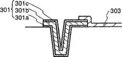
传统的反射型液晶显示器件中的像素结构示于图23。在图23中,通过布图,将两个导线、也就是栅布线(扫描线)11和电容器导线12形成为线形,源布线(信号线)14通过布图也形成为线形。当栅布线11在纵向排列时,源布线14在横向排列,在源布线14和栅布线11之间设置有层间绝缘膜以使这些导线彼此绝缘。源布线14和栅布线11彼此部分交叉。这种传统结构的特征在于包含作为有源层的半导体层10的TFT被设在了这些导线的交叉点附近。The pixel structure in a conventional reflective liquid crystal display device is shown in FIG. 23 . In FIG. 23, two wires, that is, gate wiring (scanning line) 11 and
通常,已知在源布线14之间与源布线14同时形成像素电极15。当采用这样的结构时,需要用光屏蔽膜(也称为黑衬质)13对源布线14和像素电极15之间的区来屏蔽光。Generally, it is known that the
此外,在传统结构中,将由铬等制成的金属膜布图为所需要的形状,以便得到光屏蔽膜13。采用传统方法的结果,用于形成光屏蔽膜的步骤和掩膜数量增加了。为了用光屏蔽膜13得到足够的光屏蔽,需要在光屏蔽膜13和像素电极之间设置层间绝缘膜,使它们彼此绝缘。与光屏蔽膜类似,当构成层间绝缘膜的层的数量增加时,制造步骤相应增加,导致制造费用增加。此外,层间绝缘膜的层的数量增加在层间绝缘性能的保持方面是不利的。Furthermore, in the conventional structure, a metal film made of chromium or the like is patterned into a desired shape to obtain the
对于另一种传统结构,已知的是其中将层间绝缘膜设为覆盖源布线11,在绝缘膜上再设置像素电极。然而当采用这种结构时,层的数量增加导致步骤增加,最后导致制造费用增加。As another conventional structure, there is known one in which an interlayer insulating film is set to cover the
此外,在显示性能方面,希望像素有大量的存储电容器和高的孔径比。每个像素的高孔径比提高了光线的利用效率,减小了功率消耗和显示器件的尺寸。Furthermore, in terms of display performance, pixels with a large number of storage capacitors and a high aperture ratio are desired. The high aperture ratio of each pixel improves light utilization efficiency, reduces power consumption and size of the display device.
近来,像素尺寸变得更小以得到高清晰图像。像素尺寸的减小增加了为一个像素要形成的TFT和导线的区域,因此反倒降低了像素孔径比。Recently, the pixel size has become smaller to obtain high-definition images. The reduction in pixel size increases the area of TFTs and wires to be formed for one pixel, thus conversely reducing the pixel aperture ratio.
这样,为了得到的具有确定的像素尺寸每个像素的高孔径比,有效布局对于像素的电路结构所需的电路元件是必要的。Thus, in order to obtain a high aperture ratio per pixel with a defined pixel size, an efficient layout of the circuit elements required for the circuit structure of the pixel is necessary.
如上所述,为了用少量的掩膜实现具有高孔径比的反射型液晶显示器件或透射型液晶显示器件,需要一种不同于任何传统结构的完全新颖的像素结构。As described above, in order to realize a reflective liquid crystal display device or a transmissive liquid crystal display device having a high aperture ratio with a small number of masks, a completely novel pixel structure different from any conventional structure is required.
本发明就是要满足这样的需要,在不增加掩膜数量和制造步骤的情况下,通过本发明实现具有高像素孔径比的像素结构的液晶显示器件。The present invention is to meet such needs, and realizes a liquid crystal display device with a pixel structure with a high pixel aperture ratio without increasing the number of masks and manufacturing steps.
为了解决传统技术的上述问题,设计了下面的措施。In order to solve the above-mentioned problems of the conventional technology, the following measures are devised.
本发明的特征是不用黑衬质而能对TFTs和像素之间的区屏蔽光的像素结构。本发明的特征在于,作为对TFT屏蔽光的方法之一是在第一绝缘膜上形成栅极和源布线,作为有源层的大部分半导体层由形成在不同于第一绝缘膜的第二绝缘膜上的栅布线覆盖。本发明的特征在于,并且作为对像素之间的区屏蔽光的方法之一是设置像素电极,使其与源布线交叠。此外,本发明的特征还在于,作为对TFT屏蔽光的方法之一是在相对衬底(counter substrate)上配置滤色器(红色滤色器或红色滤色器和蓝色滤色器的叠层膜)作为光屏蔽膜,使其与元件衬底(element substrate)上的TFTs交叠。The feature of the present invention is a pixel structure capable of shielding the region between TFTs and pixels from light without using a black substrate. The present invention is characterized in that, as one of the methods for shielding TFT from light, gate and source wirings are formed on the first insulating film, and most of the semiconductor layers as the active layer are formed on a second insulating film different from the first insulating film. Gate wiring covering on insulating film. The present invention is characterized in that, and as one of the methods of shielding the region between pixels from light, the pixel electrode is provided so as to overlap the source wiring. In addition, the present invention is also characterized in that, as one of the methods for shielding the TFT from light, a color filter (a red color filter or a stack of a red color filter and a blue color filter) is arranged on an opposite substrate (counter substrate). layer) as a light-shielding film that overlaps the TFTs on the element substrate.
本说明书中所公开的本发明的结构涉及半导体器件,包括:The structures of the present invention disclosed in this specification relate to semiconductor devices, including:
在绝缘表面上的半导体层(第一半导体层172),具有源区、漏区和夹在源区和漏区之间的沟道形成区;a semiconductor layer (first semiconductor layer 172) on an insulating surface, having a source region, a drain region, and a channel formation region sandwiched between the source region and the drain region;
半导体层(第一半导体层172)上的第一绝缘膜;a first insulating film on the semiconductor layer (first semiconductor layer 172);
第一绝缘膜上的电极(包含栅极的第一电极134),与沟道形成区交叠;electrodes (including the
第一绝缘膜上的源布线;source wiring on the first insulating film;
覆盖电极(包含栅极的第一电极134)和源布线的第二绝缘膜;和a second insulating film covering the electrodes (the
第二绝缘膜上的栅布线166,与电极连接(包含栅极的第一电极134)。The
此外,在本说明书中所公开的本发明的结构涉及半导体器件,包括:Furthermore, the structures of the present invention disclosed in this specification relate to semiconductor devices, including:
在绝缘表面上的半导体层(第一半导体层172),具有源区、漏区和夹在源区和漏区之间的沟道形成区;a semiconductor layer (first semiconductor layer 172) on an insulating surface, having a source region, a drain region, and a channel formation region sandwiched between the source region and the drain region;
半导体层(第一半导体层172)上的第一绝缘膜;a first insulating film on the semiconductor layer (first semiconductor layer 172);
第一绝缘膜上的电极(包含栅极134的第一电极),与沟道形成区交叠;electrodes on the first insulating film (including the first electrode of the gate electrode 134) overlapping the channel formation region;
第一绝缘膜上的源布线;source wiring on the first insulating film;
覆盖电极和源布线的第二绝缘膜;a second insulating film covering the electrodes and source wiring;
第二绝缘膜上的与电极连接的栅布线;a gate wiring connected to the electrode on the second insulating film;
第二绝缘膜上的连接电极165,连接到源布线和半导体层(具体地说是源区或漏区);和The
第二绝缘膜上的像素电极167,连接到半导体层(具体地说是源区或漏区)。The
此外,在上述结构中,排列像素电极,使其与源布线交叠,像素电极和源布线之间夹有第二绝缘膜,以此在像素电极和源布线之间屏蔽光(或减少光泄露)。Furthermore, in the above structure, the pixel electrode is arranged so as to overlap the source wiring with the second insulating film interposed between the pixel electrode and the source wiring, thereby shielding light (or reducing light leakage) between the pixel electrode and the source wiring. ).
此外,在上面提到的各个结构中,半导体器件的特征在于,半导体层具有与栅布线交叠的区,半导体层和栅布线之间夹有第一绝缘膜。Furthermore, in each of the above-mentioned structures, the semiconductor device is characterized in that the semiconductor layer has a region overlapping the gate wiring, and the first insulating film is interposed between the semiconductor layer and the gate wiring.
此外,在上述半导体层中,当半导体层和栅布线之间夹有第一绝缘膜时,与栅布线交叠的半导体层的区的特征在于,至少包含沟道形成区、位于沟道形成区和漏区之间的区、或位于沟道形成区和源区之间的区。保护这个半导体层区不受外界光线的照射。In addition, in the above-mentioned semiconductor layer, when the first insulating film is interposed between the semiconductor layer and the gate wiring, the region of the semiconductor layer overlapping the gate wiring is characterized in that it includes at least a channel formation region, and is located in the channel formation region. and a region between the drain region, or a region between the channel forming region and the source region. This semiconductor layer region is protected from external light.
在多栅结构的情况下,其中在一个半导体层上存在多个栅极,当其间夹有第一绝缘膜时,在半导体层上存在多个沟道形成区。希望设置栅布线使其与存在于一个沟道形成区和另一个沟道形成区之间的区交叠。In the case of a multi-gate structure in which a plurality of gate electrodes exist on one semiconductor layer, a plurality of channel formation regions exist on the semiconductor layer when the first insulating film is interposed therebetween. It is desirable to arrange the gate wiring so as to overlap a region existing between one channel formation region and the other channel formation region.
此外,本发明的特征在于,为了不增加掩膜数量,在第一绝缘膜上用同样的材料形成电极和源布线,在第二绝缘膜上用相同的材料形成像素电极、连接电极和栅布线。Furthermore, the present invention is characterized in that, in order not to increase the number of masks, electrodes and source wirings are formed of the same material on the first insulating film, and pixel electrodes, connection electrodes, and gate wirings are formed of the same material on the second insulating film. .
此外,在上面提到的各个结构中,半导体器件的特征在于,栅布线是由包含从已掺杂给与导电率的杂质元素的多晶硅、W、WSix、Al、Cu、Ta、Cr和Mo所构成的组中选出的元素作为主成分的膜或它们的叠层膜制成。Furthermore, in each of the structures mentioned above, the semiconductor device is characterized in that the gate wiring is made of polysilicon containing impurity elements that have been doped to give conductivity, W,WSix , Al, Cu, Ta, Cr, and Mo A film or a laminated film of them is made of elements selected from the constituting group as the main component.
此外,在上面提到的各个结构中,半导体器件的特征在于,第一电极和半导体层之间用于绝缘的第一绝缘膜是栅绝缘膜。Furthermore, in each of the structures mentioned above, the semiconductor device is characterized in that the first insulating film for insulation between the first electrode and the semiconductor layer is a gate insulating film.
此外,在上面提到的各个结构中,半导体器件的特征在于,用于绝缘源布线和栅布线的第二绝缘膜包含含硅作为主成分的第一绝缘层和由有机树脂材料制成的第二绝缘层。Furthermore, in each of the structures mentioned above, the semiconductor device is characterized in that the second insulating film for insulating the source wiring and the gate wiring includes a first insulating layer containing silicon as a main component and a second insulating layer made of an organic resin material. Two insulating layers.
此外,在上面提到的各个结构中,半导体器件的特征在于,包含像素电极的一个像素形成存储电容器,该电容器由连接到像素电极的半导体层(第二半导体层173)和连接到相邻像素的栅布线的电极(第二电极135)以及利用第一绝缘膜作为电介质构成。此外,最好将提供p型导电率的杂质元素掺杂到这个半导体层(第二半导体层173)。Furthermore, in each of the structures mentioned above, the semiconductor device is characterized in that one pixel including the pixel electrode forms a storage capacitor consisting of a semiconductor layer (second semiconductor layer 173) connected to the pixel electrode and a semiconductor layer connected to an adjacent pixel. The electrode (second electrode 135) of the gate wiring and the first insulating film are used as a dielectric. In addition, it is preferable to dope this semiconductor layer (second semiconductor layer 173) with an impurity element that provides p-type conductivity.
此外,本发明的另一个结构涉及包含TFTs的半导体器件,每个TFT包括形成在绝缘表面上的半导体层、形成在半导体层上的绝缘膜和形成在绝缘膜上的栅极,其特征在于,栅极包含作为下层的具有楔形端部的第一导电层和作为上层的具有比第一导电层的宽度更窄的第二导电层,该半导体层包含与第二导电层交叠、其间夹有绝缘膜的沟道形成区、与沟道形成区接触的第三杂质区、与第三杂质区接触的第二杂质区和与第二杂质区接触的第一杂质区。In addition, another structure of the present invention relates to a semiconductor device including TFTs each including a semiconductor layer formed on an insulating surface, an insulating film formed on the semiconductor layer, and a gate electrode formed on the insulating film, characterized in that, The gate electrode includes as a lower layer a first conductive layer having a wedge-shaped end portion and as an upper layer a second conductive layer having a width narrower than that of the first conductive layer, the semiconductor layer including an overlapped second conductive layer with a A channel formation region of the insulating film, a third impurity region in contact with the channel formation region, a second impurity region in contact with the third impurity region, and a first impurity region in contact with the second impurity region.
此外,在第一导电层的斜面和水平平面之间形成的角度(也称为楔形角)比第二导电层的斜面和水平平面之间形成的角度小。为了方便,在本说明书中,将具有楔形角的斜面称为楔形,具有楔形的部分称为楔形部分。Furthermore, the angle formed between the slope of the first conductive layer and the horizontal plane (also referred to as wedge angle) is smaller than the angle formed between the slope of the second conductive layer and the horizontal plane. For convenience, in this specification, the slope with a wedge angle is called a wedge, and the part with a wedge is called a wedge.
此外,在上述结构中,第三杂质区的特征为:与第一导电层交叠,其间夹有绝缘膜。第三杂质区是通过使杂质元素穿过其端部具有楔形部分的第一导电层和绝缘膜,从而将杂质元素掺杂到半导体层而形成的。在掺杂中,位于半导体层上的材料层越厚,离子注入越浅。因此,掺杂到半导体层的杂质浓度受具有楔形的导电层厚度影响,导致杂质元素浓度的变化。随着第一导电层的厚度增加,半导体层中的杂质浓度降低。同样,随着第一导电层的厚度降低,半导体层中的杂质浓度增加。Furthermore, in the above structure, the third impurity region is characterized by overlapping the first conductive layer with the insulating film interposed therebetween. The third impurity region is formed by doping the impurity element into the semiconductor layer by passing the impurity element through the first conductive layer and the insulating film having the tapered portion at its end. In doping, the thicker the layer of material on top of the semiconductor layer, the shallower the ion implantation. Therefore, the impurity concentration doped into the semiconductor layer is affected by the thickness of the conductive layer having a wedge shape, resulting in variation in the concentration of impurity elements. As the thickness of the first conductive layer increases, the impurity concentration in the semiconductor layer decreases. Also, as the thickness of the first conductive layer decreases, the impurity concentration in the semiconductor layer increases.
此外,在上述结构中,半导体器件的特征在于,第一杂质区是源区或漏区。Furthermore, in the above structure, the semiconductor device is characterized in that the first impurity region is a source region or a drain region.
此外,在上述结构中,半导体器件的特征在于,与第二杂质区交叠的绝缘膜的区包含楔形部分。第二杂质区是通过穿过绝缘膜将杂质元素注入半导体层而形成的。因此,第二杂质区的杂质浓度受绝缘膜的楔形部分影响,使第二杂质区的杂质浓度分布变化。随着绝缘膜的厚度增加,第二杂质区中的杂质浓度降低。同样,随着绝缘膜的厚度降低,第二杂质区中的杂质浓度增大。尽管第二杂质区与第三杂质区一样是通过掺杂形成的,由于第二杂质区不与第一导电层交叠,因此第二杂质区中的杂质浓度比第三杂质区中的杂质浓度高。在沟道的纵向上,第二杂质区的宽度与第三杂质区的宽度一样,或比第三杂质区的宽度宽。Further, in the above structure, the semiconductor device is characterized in that the region of the insulating film overlapping the second impurity region includes a wedge-shaped portion. The second impurity region is formed by implanting an impurity element into the semiconductor layer through the insulating film. Therefore, the impurity concentration of the second impurity region is affected by the wedge-shaped portion of the insulating film, so that the impurity concentration distribution of the second impurity region varies. As the thickness of the insulating film increases, the impurity concentration in the second impurity region decreases. Also, as the thickness of the insulating film decreases, the impurity concentration in the second impurity region increases. Although the second impurity region is formed by doping like the third impurity region, since the second impurity region does not overlap the first conductive layer, the impurity concentration in the second impurity region is higher than that in the third impurity region. high. In the longitudinal direction of the channel, the width of the second impurity region is the same as or wider than that of the third impurity region.
此外,上述结构的特征在于,TFT是n沟道TFT或p沟道TFT。而且,在本发明中,用n沟道TFT形成像素TFT。另外,用这些n沟道TFTs或p沟道TFTs形成包含CMOS电路的驱动电路。Furthermore, the above structure is characterized in that the TFT is an n-channel TFT or a p-channel TFT. Also, in the present invention, pixel TFTs are formed with n-channel TFTs. In addition, a driver circuit including a CMOS circuit is formed using these n-channel TFTs or p-channel TFTs.
而且,在本说明书中所公开的本发明的结构涉及一种半导体器件,包括一对衬底和保持在这对衬底之间的液晶。Also, the structure of the present invention disclosed in this specification relates to a semiconductor device including a pair of substrates and a liquid crystal held between the pair of substrates.
其特征在于在这对衬底之一上提供像素部分和驱动电路,和characterized in that a pixel portion and a driver circuit are provided on one of the pair of substrates, and
像素部分包含:The pixel section contains:
绝缘表面上的半导体层,包含源区、漏区和夹在源区和漏区之间的沟道形成区;a semiconductor layer on an insulating surface comprising a source region, a drain region and a channel forming region sandwiched between the source region and the drain region;
半导体层上的第一绝缘膜;a first insulating film on the semiconductor layer;
第一绝缘膜上的电极,与沟道形成区交叠;an electrode on the first insulating film overlapping the channel formation region;
在第一绝缘膜上的源布线;source wiring on the first insulating film;
第二绝缘膜,覆盖电极和源布线;a second insulating film covering the electrodes and source wiring;
第二绝缘膜上的栅布线,连接到电极;a gate wiring on the second insulating film, connected to the electrode;
第二绝缘膜上的连接电极,连接到源布线和半导体层;和a connection electrode on the second insulating film, connected to the source wiring and the semiconductor layer; and
第二绝缘膜上的像素电极,连接到半导体层,以及a pixel electrode on the second insulating film, connected to the semiconductor layer, and
另一个衬底具有光屏蔽膜,其中将红色滤色器和蓝色滤色器层叠使其与第一半导体层交叠。The other substrate has a light-shielding film in which a red color filter and a blue color filter are laminated so as to overlap the first semiconductor layer.
此外,在上述结构中,该半导体器件提供了一种IPS型液晶显示器件,包括第二绝缘膜上的公用导线,其中配置像素电极和公用导线,使得产生平行于衬底表面的电场。Furthermore, in the above structure, the semiconductor device provides an IPS type liquid crystal display device including a common wire on the second insulating film, wherein the pixel electrode and the common wire are arranged such that an electric field parallel to the surface of the substrate is generated.
此外,在上述结构中,提供了反射型液晶显示器件,其中像素电极由包含铝或银作主成分的膜或它们的叠层膜制成。Furthermore, in the above structure, there is provided a reflection type liquid crystal display device in which the pixel electrode is made of a film containing aluminum or silver as a main component or a laminated film thereof.
此外,在上述结构中,该半导体器件提供了透射型液晶显示器件,其中像素电极由透明导电膜制成。Furthermore, in the above structure, the semiconductor device provides a transmission type liquid crystal display device in which the pixel electrode is made of a transparent conductive film.
此外,作为本发明的另一特征,本发明的半导体器件的特征在于,分别在不同的绝缘膜上形成包含栅极的第一电极134和栅布线166,在第一绝缘膜上形成第一电极134和源布线137,在不同于第一绝缘膜的第二绝缘膜上形成栅布线166和像素电极167。In addition, as another feature of the present invention, the semiconductor device of the present invention is characterized in that the
此外,在实现上述结构的制造工艺中,本发明的结构涉及制造半导体器件的方法,其特征包括:In addition, in the manufacturing process for realizing the above-mentioned structure, the structure of the present invention relates to a method of manufacturing a semiconductor device, and its features include:
第一步,在绝缘表面上,由晶体半导体膜形成半导体层;In a first step, forming a semiconductor layer from a crystalline semiconductor film on the insulating surface;
第二步,在半导体层上,形成第一绝缘膜;The second step is to form a first insulating film on the semiconductor layer;
第三步,在第一绝缘膜上,形成与半导体层和源布线交叠的电极;In a third step, forming an electrode overlapping the semiconductor layer and the source wiring on the first insulating film;
第四步,形成覆盖电极和源布线的第二绝缘膜;以及A fourth step, forming a second insulating film covering the electrodes and source wiring; and
第五步,形成连接到电极并与第二绝缘膜上的半导体层交叠的栅布线、用于连接半导体层与源布线的连接电极,和与源布线交叠的像素电极。In the fifth step, a gate wiring connected to the electrode and overlapping the semiconductor layer on the second insulating film, a connection electrode for connecting the semiconductor layer and the source wiring, and a pixel electrode overlapping the source wiring are formed.
此外,在实现上述结构的制造工艺中,本发明的另一结构涉及制造半导体器件的方法,其特征包括:In addition, in the manufacturing process for realizing the above-mentioned structure, another structure of the present invention relates to a method of manufacturing a semiconductor device, which is characterized by comprising:
第一步,在绝缘表面上形成第一半导体层172和第二半导体层173,每一层都由晶体半导体膜制成;In a first step, a first semiconductor layer 172 and a second semiconductor layer 173 are formed on the insulating surface, each layer being made of a crystalline semiconductor film;
第二步,在第一和第二半导体层上,形成第一绝缘膜;In the second step, forming a first insulating film on the first and second semiconductor layers;
第三步,形成与第一半导体层交叠的第一电极134、与第二半导体层交叠的第二电极135、和第一绝缘膜上的源布线137。In the third step, the
第四步,形成覆盖第一电极134、第二电极135和源布线137的第二绝缘膜;以及Fourth step, forming a second insulating film covering the
第五步,在第二绝缘膜上,形成连接到第一电极134并与第一半导体层172交叠的栅布线166、用于连接第一半导体层与源布线的连接电极165和与源布线交叠的像素电极167。In the fifth step, on the second insulating film, a
此外,在上述结构中,该方法的特征在于连接到像素电极的半导体层与连接到相邻像素的栅布线的第二电极交叠。Further, in the above structure, the method is characterized in that the semiconductor layer connected to the pixel electrode overlaps the second electrode connected to the gate wiring of the adjacent pixel.
在附图中in the attached picture
图1是根据本发明的像素部分的顶视图(实施例1);Fig. 1 is the top view (embodiment 1) of the pixel part according to the present invention;
图2A至2C是表示有源矩阵衬底的制造工艺的示意图(实施例1);2A to 2C are schematic diagrams representing a manufacturing process of an active matrix substrate (embodiment 1);
图3A至3C是表示有源矩阵衬底的制造工艺的示意图(实施例1);3A to 3C are schematic diagrams representing a manufacturing process of an active matrix substrate (embodiment 1);
图4是表示有源矩阵衬底的制造工艺的示意图(实施例1);Fig. 4 is the schematic diagram (embodiment 1) that represents the manufacturing process of active matrix substrate;
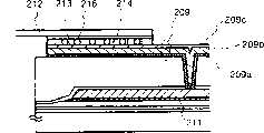
图5是表示反射型液晶显示器件的截面结构示意图(实施例2);Fig. 5 is a schematic cross-sectional structure representation (embodiment 2) of reflective liquid crystal display device;
图6是根据本发明的像素部分的顶视图(实施例1);6 is a top view of a pixel portion according to the present invention (Embodiment 1);
图7A和7B分别是有源矩阵衬底的顶视图和截面图(实施例3);7A and 7B are respectively a top view and a sectional view (embodiment 3) of an active matrix substrate;
图8A和83是端子部分的截面图(实施例3);8A and 83 are sectional views of the terminal portion (embodiment 3);
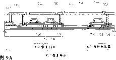
图9A至9C是显示透射型液晶显示器件的截面结构示意图(实施例4);9A to 9C are schematic cross-sectional structures showing a transmissive liquid crystal display device (embodiment 4);
图10是端子部分的截面图(实施例5);Fig. 10 is a sectional view of a terminal part (embodiment 5);
图11是根据本发明的有源矩阵衬底的截面图(实施例6);Fig. 11 is the sectional view (embodiment 6) of active matrix substrate according to the present invention;
图12是根据本发明的有源矩阵衬底的截面图(实施例7);Fig. 12 is the sectional view (embodiment 7) of active matrix substrate according to the present invention;
图13是根据本发明的像素部分的顶视图(实施例8);13 is a top view of a pixel portion according to the present invention (Embodiment 8);
图14是根据本发明的像素部分的截面视图(实施例8);14 is a cross-sectional view of a pixel portion according to the present invention (Embodiment 8);
图15是根据本发明的像素部分的顶视图(实施例10);Fig. 15 is a top view of a pixel portion according to the present invention (embodiment 10);
图16是根据本发明的像素部分的截面视图(实施例10);16 is a sectional view of a pixel portion according to the present invention (Embodiment 10);
图17是根据本发明的像素部分的顶视图(实施例11);17 is a top view of a pixel portion according to the present invention (Embodiment 11);
图18是根据本发明的像素部分的截面视图(实施例11);18 is a sectional view of a pixel portion according to the present invention (Embodiment 11);
图19是根据本发明的像素部分的截面视图(实施例12);19 is a sectional view of a pixel portion according to the present invention (Embodiment 12);
图20A至20F是表示电设备实例的示意图(实施例13);20A to 20F are schematic diagrams showing an example of an electric device (Embodiment 13);
图21A至21D是表示电设备实例的示意图(实施例13);21A to 21D are schematic diagrams showing an example of an electric device (Embodiment 13);
图22A至22C是表示电设备实例的示意图(实施例13);22A to 22C are schematic diagrams showing an example of an electric device (Embodiment 13);
图23是表示传统实例的示意图;Fig. 23 is a schematic diagram showing a conventional example;
图24A至24D是表示有源矩阵衬底制造方法的放大的截面视图;以及24A to 24D are enlarged cross-sectional views showing an active matrix substrate manufacturing method; and
图25是像素部分的顶视图(实施例4)。Fig. 25 is a top view of a pixel portion (Embodiment 4).
下面将参考附图描述本发明的实施例。Embodiments of the present invention will be described below with reference to the drawings.
作为基本结构,本发明的液晶显示器件包含元件衬底和相对衬底,在衬底之间留有预定间隙并相互粘接以及容纳在间隙中的光电材料(液晶材料或其类似物)。As a basic structure, the liquid crystal display device of the present invention comprises an element substrate and an opposing substrate with a predetermined gap between them and bonded to each other and a photoelectric material (liquid crystal material or the like) accommodated in the gap.
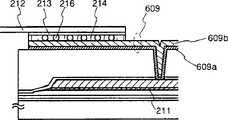
图1示出了根据本发明的像素结构的具体实例。这里示出的是反射型液晶显示器件的一个实例。FIG. 1 shows a specific example of a pixel structure according to the present invention. Shown here is an example of a reflective liquid crystal display device.
元件衬底包含横向排列的栅布线166、纵向排列的源布线137、具有在栅布线166和源布线137的交点附近的具有像素TFT的像素部分,以及具有n沟道TFT或p沟道TFT的驱动电路。The element substrate includes a
图1中示出的栅布线166连接到在横向排列的岛状第一电极134。栅极布线166设置在与之接触的第二绝缘膜上。源布线137与之类似,岛状第一电极134形成在与之接触的第一绝缘膜(也是下文的栅绝缘膜)上。The
连接电极165就像像素电极167、175和栅布线166那样形成在第二绝缘膜(也是下文的层间绝缘膜)上。The
由于本发明的像素结构,可以使TFT的有源层与栅布线交叠,从而使TFT的有源层屏蔽光。Due to the pixel structure of the present invention, it is possible to cause the active layer of the TFT to overlap the gate wiring, thereby shielding the active layer of the TFT from light.
为了达到为电极衬底上的TFT屏蔽光的目的,至少要将第一半导体层172的沟道形成区设置在能由栅布线166来屏蔽光线的位置。除了沟道形成区,希望存在于沟道形成区和漏区(例如LDD区和偏移区)之间的区以及存在于沟道形成区和源区之间的区也由栅布线166来屏蔽光线。由于图1所示的像素结构是多栅极结构,多个沟道形成区存在于一个半导体层中。因此,还希望存在于一个沟道形成区和另一个沟道形成区之间的区也由栅布线166屏蔽光线。In order to achieve the purpose of shielding the TFT on the electrode substrate from light, at least the channel formation region of the first semiconductor layer 172 should be arranged at a position where light can be shielded by the
栅布线166以接触的方式形成在绝缘膜上,该绝缘膜不同于在其上提供作为栅电极的第一电极134的绝缘膜。在图1所示的像素结构中,第一电极134不仅作为穿过栅绝缘膜与第一半导体层交叠的栅电极,而且作为构成相邻像素的存储电容器的一个电极。The
具有本发明的像素结构,像素之间的区主要通过将像素电极167的端部与源布线137交叠来屏蔽光线。With the pixel structure of the present invention, the region between pixels shields light mainly by overlapping the end of the
间隙,例如像素电极167和连接电极165之间的间隙以及像素电极167和栅布线166之间的间隙都通过设置在相对衬底上的滤色器来屏蔽光线。对于布图在预导向置(在元件衬底上TFT的位置)的滤色器,包括在相对衬底上提供的红色滤色器、红色滤色器和兰色滤色器的叠层膜、或红色滤色器的叠层膜、兰色滤色器以及绿色滤色器。Gaps, such as the gap between the
具有这样的结构,元件衬底上的TFT主要通过栅布线166屏蔽光线。而且,像素之间的间隙可以通过设置在相对衬底上的滤色器(红色滤色器、红色滤色器和兰色滤色器的叠层膜,或红色滤色器的叠层膜、蓝色滤色器和绿色滤色器)来屏蔽光线。With such a structure, the TFT on the element substrate is mainly shielded from light by the
像素电极167的存储电容器是通过连接到像素电极167的第二半导体层173和第二电极135构成,利用覆盖第二半导体层173的绝缘膜作为电介质。将提供p型导电率的杂质元素掺杂到第二半导体层173的一部分。掺杂的结果是当电压加到第二电极135时,形成了沟道形成区,从而形成存储电容器。而且,在第二电极135与像素电极167交叠的区域中,形成了用层间绝缘膜157和158作为电介质的存储电容器。尽管这里的存储电容器是用第二电极135形成的,但并非特别限制存贮电容器;可以有选择地采用其中提供了电容器导线或电容器电极的像素结构。The storage capacitor of the
形成元件衬底所需的掩膜数量可设为5,其中元件衬底包含具有图1所示的像素结构的像素部分和驱动电路。具体地说,第一掩膜用来布图第一半导体层172和第二半导体层173;第二掩膜用来布图第一电极134、第二电极135和源布线137;当掺杂提供p型导电率的杂质元素以形成p沟道TFT和驱动电路的存储电容器时,第三掩膜用来覆盖n沟道TFT;第四掩膜用来形成到达第一半导体层、第二半导体层、第一电极和第二电极的接触孔;第五掩膜用来布图连接电极165和205、栅布线166、像素电极167和175。The number of masks required to form an element substrate including a pixel portion having the pixel structure shown in FIG. 1 and a driving circuit can be set to five. Specifically, the first mask is used to pattern the first semiconductor layer 172 and the second semiconductor layer 173; the second mask is used to pattern the
就像上面所描述的,当采用图1所示的像素结构时,可以用少量的掩膜得到高像素孔径比(大约78%)的反射型液晶显示器件。As described above, when the pixel structure shown in FIG. 1 is adopted, a reflective liquid crystal display device with a high pixel aperture ratio (about 78%) can be obtained with a small number of masks.
如果用透明导电膜作像素电极,需要另外的掩膜以布图成所希望的形状。然而,可以用该方法制造透射型的液晶显示器件。同样,当制造透射型液晶显示器件时,也可以用少量的掩膜得到大约56%的像素孔径比。If a transparent conductive film is used as the pixel electrode, an additional mask is required for patterning into a desired shape. However, a transmissive liquid crystal display device can be manufactured by this method. Likewise, when manufacturing a transmissive liquid crystal display device, a pixel aperture ratio of about 56% can also be obtained with a small number of masks.
公用导线和像素电极的设置要使得产生平行于衬底表面的电场,由此来制造IPS系统的透射型液晶显示器件。The arrangement of the common wires and the pixel electrodes is such that an electric field parallel to the surface of the substrate is generated, thereby manufacturing the transmissive liquid crystal display device of the IPS system.
通过下面的实施例将进一步详细描述具有上述结构的本发明。The present invention having the above structure will be further described in detail by the following examples.
[实施例1][Example 1]
实施例1中详细解释了同时在同一个衬底上制造像素部分和驱动电路的TFTs(n沟道TFT和p沟道TFT)的方法,其中驱动电路的TFTs是形成在像素部分周围的。Embodiment 1 explains in detail the method of simultaneously manufacturing the pixel portion and the TFTs (n-channel TFT and p-channel TFT) of the driver circuit on the same substrate, wherein the TFTs of the driver circuit are formed around the pixel portion.
首先,如图2A所示,利用如氧化硅膜、氮化硅膜或氮氧化硅膜之类的绝缘膜制成的基膜101形成在由例如硼硅酸钡玻璃或硼硅酸铝玻璃之类的玻璃制成的衬底100上,典型的玻璃如Corning公司的#7059玻璃或#1737玻璃。例如,形成用等离子CVD来由SiH4、NH3和N2O制造的厚10到200nm(最好在50和100nm之间)的氮氧化硅膜101a的叠层膜,以及用相同的方法由SiH4和N2O制造厚50到200nm(最好在100和150nm之间)的氢化氮氧化硅膜101b。实施例1中示出了基膜101的两层结构,但也可以形成单层膜和两层以上的叠层膜结构。First, as shown in FIG. 2A, a base film 101 made of an insulating film such as a silicon oxide film, a silicon nitride film, or a silicon oxynitride film is formed on a substrate made of, for example, barium borosilicate glass or aluminum borosilicate glass. The substrate 100 is made of glass, such as #7059 glass or #1737 glass of Corning Company. For example, a laminated film of silicon oxynitride film 101a made of SiH4 , NH3 and N2 O with a thickness of 10 to 200 nm (preferably between 50 and 100 nm) is formed by plasma CVD, and the same method is formed by SiH4 and N2 O produce a hydrogenated silicon oxynitride film 101b with a thickness of 50 to 200 nm (preferably between 100 and 150 nm). In Example 1, a two-layer structure of the base film 101 was shown, but a single-layer film and a laminated film structure of two or more layers may also be formed.
用激光结晶法或公知的热结晶法,从具有非晶结构的半导体膜制造晶体半导体膜,通过晶体半导体膜形成岛状半导体层102至106。岛状半导体膜102至106的厚度可以从25到80nm(最好在30nm和60nm之间)。对于晶体半导体膜材料没有限制,但最好用硅或硅锗合金(SiGe)来形成晶体半导体膜。A crystalline semiconductor film is produced from a semiconductor film having an amorphous structure by a laser crystallization method or a known thermal crystallization method, and island-shaped semiconductor layers 102 to 106 are formed through the crystalline semiconductor film. The thickness of the island-shaped semiconductor films 102 to 106 can be from 25 to 80 nm (preferably between 30 nm and 60 nm). There is no limitation on the material of the crystalline semiconductor film, but silicon or silicon germanium alloy (SiGe) is preferably used to form the crystalline semiconductor film.
可以用激光作为用激光结晶法制造晶体半导体膜的激光源,所述激光例如脉冲透射型或连续透射型准分子激光、YAG激光或YVO4激光。当用这些类型的激光时,可以用通过光学系统将从激光器发射的激光会聚成线形,然后将激光照到半导体膜的方法。可以由操作者合理地选择结晶化条件,但当用准分子激光时,脉冲发射频率设到30Hz,并且激光的能量强度设为从100mJ/cm2到400mJ/cm2(典型地在200mJ/cm2和300mJ/cm2之间)。此外,当用YAG激光时,利用其第二谐波,并且脉冲发射频率设为从1Hz到10kHz,激光的能量强度可以设为从300J/cm2到600J/cm2(典型地在350mJ/cm2和500mJ/cm2之间)。然后将会聚成线形、具有100μm至1000μm例如400μm宽度的激光照到衬底的整个表面上,用80%到98%的线形激光覆盖率完成上述过程。A laser such as a pulse transmission type or continuous transmission type excimer laser, a YAG laser or a YVO4 laser can be used as a laser source for producing a crystalline semiconductor film by a laser crystallization method. When using these types of lasers, a method of condensing laser light emitted from a laser into a line by an optical system and then irradiating the laser light onto a semiconductor film can be used. The crystallization conditions can be reasonably selected by the operator, but when an excimer laser is used, the pulse emission frequency is set to 30 Hz, and the energy intensity of the laser is set from 100 mJ/cm to 400 mJ/cm (typically at 200 mJ/cm2 and 300mJ/cm2 ). In addition, when using YAG laser, using its second harmonic, and the pulse emission frequency is set from 1Hz to 10kHz, the energy intensity of the laser can be set from 300J/cm2 to 600J/cm2 (typically at 350mJ/cm2 and 500mJ/cm2 ). Then laser light focused in a line shape with a width of 100 μm to 1000 μm, for example 400 μm, is irradiated onto the entire surface of the substrate, and the above process is completed with a line laser coverage of 80% to 98%.
形成覆盖在岛状半导体层102至106上的栅绝缘膜107。栅绝缘膜107是用包含硅、厚度为40至150nm的绝缘膜,通过等离子体CVD或溅射法形成。在实施例1中形成了厚120nm的氮氧化硅膜。栅绝缘膜并不限于这种氮氧化硅膜,当然可以用其它包含硅的绝缘膜,也可以采用单层或叠层结构。例如,当用氧化硅膜时,可以在40Pa的反应压力下,将衬底温度设为300℃至400℃,在0.5至0.8W/cm2的电功率系数下,通过高频(13.56MHz)放电,用TEOS(原硅酸四乙酯)和O2的混合物,通过等离子VD形成氧化硅膜。经过后续的对氧化硅膜进行温度在400℃至500℃之间的热退火,就得到了具有优异特性的栅绝缘膜。A gate insulating film 107 is formed covering the island-shaped semiconductor layers 102 to 106 . The gate insulating film 107 is formed of an insulating film containing silicon and having a thickness of 40 to 150 nm by plasma CVD or sputtering. In Example 1, a silicon oxynitride film was formed to a thickness of 120 nm. The gate insulating film is not limited to this silicon oxynitride film, and of course other insulating films containing silicon may be used, and a single-layer or stacked-layer structure may also be used. For example, when a silicon oxide film is used, the substrate temperature can be set at 300°C to 400°C under a reaction pressure of 40Pa, and the electric power coefficient of 0.5 to 0.8W/cm2 can be discharged by high frequency (13.56MHz) , using a mixture of TEOS (tetraethyl orthosilicate) and O2 to form a silicon oxide film by plasma VD. After subsequent thermal annealing of the silicon oxide film at a temperature between 400° C. and 500° C., a gate insulating film with excellent characteristics is obtained.
然后为了形成栅极,在栅绝缘膜107上形成第一导电膜108和第二导电膜109。在实施例1中,第一导电膜是用钽膜形成的,具有50至100nm的厚度,第二导电膜是用钨膜形成的,具有100至300nm的厚度。Then, to form a gate, a first conductive film 108 and a second conductive film 109 are formed on the gate insulating film 107 . In Embodiment 1, the first conductive film is formed of a tantalum film and has a thickness of 50 to 100 nm, and the second conductive film is formed of a tungsten film and has a thickness of 100 to 300 nm.
TaN膜是用溅射法,即在氮气氛中进行钽靶的溅射形成的。钨膜是用钨靶通过溅射形成的,也可以用六氟化钨(WF6)通过热CVD来形成。为了用它作为栅极,无论用哪种方法,都必须使膜的电阻变低,最好使钨膜的电阻率等于或低于20μΩ.cm。电阻率可以通过扩大钨膜的晶粒来使其降低,但在钨膜中有许多杂质元素例如氧的情况下,结晶被抑制,膜变成了高阻膜。因此,在溅射中,采用99.9999%或99.99%纯度的钨靶。此外,在钨膜的形成过程中,当充分注意了在膜形成时没有从气相引入杂质时,可以得到9至20μΩ.cm的电阻率。The TaN film is formed by sputtering, that is, sputtering a tantalum target in a nitrogen atmosphere. The tungsten film is formed by sputtering using a tungsten target, or by thermal CVD using tungsten hexafluoride (WF6 ). In order to use it as a gate, no matter which method is used, the resistance of the film must be made low, and it is preferable to make the resistivity of the tungsten film equal to or lower than 20μΩ.cm. The resistivity can be lowered by enlarging the crystal grains of the tungsten film, but in the case where there are many impurity elements such as oxygen in the tungsten film, the crystallization is suppressed and the film becomes a high-resistance film. Therefore, in sputtering, a 99.9999% or 99.99% pure tungsten target is used. Furthermore, in the formation of the tungsten film, when sufficient care is taken not to introduce impurities from the gas phase at the time of film formation, a resistivity of 9 to 20 µΩ·cm can be obtained.
需要说明的是,尽管在实施例1中第一导电膜108是钽膜,第二导电膜是钨膜,但导电膜并不限于这些。这两个导电膜也可以用下列材料形成,这些材料是:从由钽、钨、钛、钼、铝和铜所组成的组中选出的元素,从由上述元素中的一个作为主成分构成的合金材料中选出的合金材料,或从上述元素的化合物中选出的化合物材料。而且,也可以用半导体膜,典型的是其中掺杂了杂质元素例如磷的多晶硅膜。除了实施例1所用的组合之外,其它最佳组合的例子包含:用氮化钽(TaN)形成第一导电膜,将其与由钨膜形成的第二导电膜相结合;用氮化钽(TaN)形成第一导电膜,将其与由铝膜形成的第二导电膜相结合;和用氮化钽(TaN)形成第一导电膜,将其与由铜膜形成的第二导电膜相结合。It should be noted that although the first conductive film 108 is a tantalum film and the second conductive film is a tungsten film in Embodiment 1, the conductive films are not limited to these. These two conductive films may also be formed with materials selected from the group consisting of tantalum, tungsten, titanium, molybdenum, aluminum, and copper, consisting of one of the above elements as a main component. Alloy materials selected from alloy materials, or compound materials selected from compounds of the above elements. Furthermore, a semiconductor film, typically a polysilicon film into which an impurity element such as phosphorus is doped, may also be used. In addition to the combination used in Embodiment 1, examples of other optimum combinations include: forming the first conductive film with tantalum nitride (TaN), combining it with a second conductive film formed of tungsten film; (TaN) forming the first conductive film, combining it with the second conductive film formed of the aluminum film; and forming the first conductive film with tantalum nitride (TaN), combining it with the second conductive film formed of the copper film Combine.
下一步由抗蚀剂形成掩膜110至116,为了形成电极和导线,进行第一刻蚀工序。实施例1中用ICP(电感耦合等离子体)刻蚀法,即用CF4和Cl2的混合气体作为刻蚀气体,在1Pa(压力下)通过给线圈形电极施加500W的射频(RF)电功率(13.56MHz),产生等离子体,又施加100W的RF电功率到衬底的侧面(测试片部分),有效地施加了负的自偏压。在混合CF4和Cl2的情况下,将钨膜和氮化钽膜刻蚀到接近同一水平线。Next, masks 110 to 116 are formed from a resist, and a first etching process is performed in order to form electrodes and wires. Use ICP (inductively coupled plasma) etching method in embodiment 1, promptly use CF4 and Cl2 The mixed gas is as etching gas, at 1Pa (under pressure) by applying the radio frequency (RF) electric power of 500W to the coil shape electrode (13.56 MHz), plasma was generated, and 100 W of RF electric power was applied to the side surface of the substrate (the test piece portion), effectively applying a negative self-bias. In the case of mixing CF4 and Cl2 , the tungsten film and the tantalum nitride film were etched close to the same level.
用合适的抗蚀剂掩膜图形,在上述刻蚀条件下,根据施加到衬底侧面的偏压的效应,使第一导电层和第二导电层的边缘部分成为楔形,楔形部分的角度从15°到45°。完成腐蚀后,为了在栅绝缘膜上没有任何剩余,可以增加大约10%到20%的刻蚀时间。氮氧化硅膜相对于钨膜的选择率从2到4(典型的是3),因此用这种过刻蚀工艺,能够将氮氧化硅膜的暴露表面刻蚀大约20至50nm。这样,根据第一刻蚀工序,就形成了由第一导电层和第二导电层形成的第一形状的导电层118至124(第一导电层118a至124a和第二导电层118b至124b)。参考标号117代表栅绝缘膜,通过20至50nm的刻蚀,使栅绝缘膜117的没有被第一形状的导电层118至124覆盖的区域变得更薄。With a suitable resist mask pattern, under the above-mentioned etching conditions, according to the effect of the bias voltage applied to the side of the substrate, the edge portions of the first conductive layer and the second conductive layer become wedge-shaped, and the angle of the wedge-shaped portion is from 15° to 45°. After the etching is completed, the etching time may be increased by about 10% to 20% so that nothing remains on the gate insulating film. The selectivity of the silicon oxynitride film to the tungsten film is from 2 to 4 (typically 3), so with this overetching process, the exposed surface of the silicon oxynitride film can be etched by about 20 to 50 nm. Thus, according to the first etching process, the first-shaped conductive layers 118 to 124 (first conductive layers 118a to 124a and second conductive layers 118b to 124b) formed of the first conductive layer and the second conductive layer are formed. . Reference numeral 117 denotes a gate insulating film, and regions of the gate insulating film 117 not covered by the conductive layers 118 to 124 of the first shape are made thinner by etching of 20 to 50 nm.
此外,实施例1中的第一形状导电层118至124是用一次刻蚀形成的,但它们也可以通过多次刻蚀来形成。Furthermore, the first shape conductive layers 118 to 124 in Embodiment 1 are formed by one etching, but they may also be formed by multiple etchings.
然后进行第一掺杂工序,添加提供n型导电率的杂质元素。(看图2B)掺杂的方法可以采用离子掺杂或离子注入。离子掺杂是在掺杂量从1×10¹³至5×10¹⁴原子/cm2和60至100keV的加速电压条件下进行的。用周期表15族元素,典型的是磷(P)或砷(As),作为提供n型导电率的杂质元素,这里用的是磷(P)。在这种情况下,就n型导电率而言,导电层118至122变为给予杂质元素的掩膜,以自对准方式形成第一杂质区125至129。将提供n型导电率的杂质元素掺杂到第一杂质区125至129,浓度在1×1020至1×1021原子/cm3的范围内。A first doping step is then performed to add impurity elements that provide n-type conductivity. (See Figure 2B) The method of doping can be ion doping or ion implantation. Ion doping was performed under the conditions of a doping amount ranging from 1×10¹³ to 5×10¹⁴ atoms/cm2 and an accelerating voltage of 60 to 100 keV. A
下面进行第二刻蚀工序,如图2C所示。同样用ICP刻蚀方法,用CF4、Cl2和O2的混合物作为刻蚀气体,在1Pa的压力下,通过给线圈形电极施加500W的射频电功率(13.56MHz),产生等离子体,又将50W(13.56MHz)的射频电功率施加到衬底的侧面(测试片部分),就施加了比第一刻蚀工序更低的自偏压。在上述刻蚀条件下对钨膜进行各向异性刻蚀,对钽(第一导电层)以更慢的刻蚀速度进行各向异性刻蚀,形成第二形状的导电层131至137(第一导电层131a至137a和第二导电层131b至137b)。参考标号130代表栅绝缘膜,没有被第二形状的导电层131至137覆盖的区域另外再刻蚀大约20至50nm,形成更薄的区。Next, a second etching process is performed, as shown in FIG. 2C . Also use the ICP etching method, use the mixture of CF4 , Cl2 and O2 as the etching gas, and apply 500W radio frequency electric power (13.56MHz) to the coil-shaped electrode under the pressure of 1Pa to generate plasma, and the The RF power of 50W (13.56MHz) was applied to the side of the substrate (the test piece part), and a lower self-bias voltage was applied than in the first etching process. Under the above-mentioned etching conditions, the tungsten film is anisotropically etched, and the tantalum (first conductive layer) is anisotropically etched at a slower etching rate to form conductive layers 131 to 137 of the second shape (the first conductive layer). a conductive layer 131a to 137a and a second conductive layer 131b to 137b). Reference numeral 130 denotes a gate insulating film, and regions not covered by the conductive layers 131 to 137 of the second shape are additionally etched by about 20 to 50 nm to form thinner regions.
此外,实施例1中图2C所示的第二形状的导电层131至137是用一次刻蚀形成的,但它们也可以通过刻蚀两次或更多次来形成,例如,在用CF4和Cl2的气体混合物刻蚀后,还可以用CF4、Cl2和O2的气体混合物再进行刻蚀。In addition, the conductive layers 131 to 137 of the second shape shown in FIG. 2C in Embodiment 1 are formed by one etching, but they may also be formed by etching two or more times, for example, when using CF4 After etching with a gas mixture of CF4 , Cl 2 and O 2 , etching can also be performed with a gas mixture of CF4 , Cl2 and O2 .
在CF4和Cl2混合气体作用下,W膜或TaN膜的刻蚀反应可以通过产生的自由基和离子型以及反应产物的蒸汽压来评估。比较钨和钽的氟化物和氯化物的蒸汽压,钨的氟化物(WF6)(的蒸汽压)非常高,WCl5、TaF5和TaCl5的蒸汽压具有相同的量级。因此钨膜和钽膜都用CF4和Cl2的混合气体来刻蚀。然而,如果往气体混合物中添加适量的O2,CF4和O2反应,就形成CO和F,并产生大量的F自由基或F离子。结果,提高了具有高氟化物蒸汽压的钨膜的刻蚀速度。另一方面,即使F增加了,钽的刻蚀速度不会相对提高。此外,相对于W,TaN更容易氧化,因此由于O2的添加,氧化了TaN的表面。由于TaN的氧化物不与氟和氯反应,因此进一步降低了TaN膜的刻蚀速度。因此使W膜和TaN膜具有不同的刻蚀速度变为可能,也使W膜的刻蚀速度比TaN膜的刻蚀速度大变为可能。Under the action of CF4 and Cl2 mixed gas, the etching reaction of W film or TaN film can be evaluated by the generated free radicals and ions and the vapor pressure of the reaction products. Comparing the vapor pressures of tungsten and tantalum fluorides and chlorides, tungsten fluoride (WF6 ) is very high, and the vapor pressures of WCl5 , TaF5 and TaCl5 are of the same order. Therefore, both the tungsten film and the tantalum film are etched with the mixed gas of CF4 and Cl2 . However, if an appropriate amount of O2 is added to the gas mixture, CF4 reacts with O2 to form CO and F, and generate a large number of F radicals or F ions. As a result, the etching rate of the tungsten film having a high fluoride vapor pressure is increased. On the other hand, even if F increases, the etch rate of tantalum will not increase relatively. In addition, TaN is more easily oxidized relative to W, so the surface of TaN is oxidized due to the addition ofO2 . Since the oxide of TaN does not react with fluorine and chlorine, the etching rate of the TaN film is further reduced. Therefore, it becomes possible to have different etching rates for the W film and the TaN film, and it is also possible to make the etching rate of the W film larger than that of the TaN film.
然后进行第二掺杂工序,如图3A所示。在这种情况下,使掺杂量比第一掺杂工序的掺杂量小,在高加速电压的条件下来掺杂提供n型导电率的杂质元素。例如,用70至120keV的加速电压和1×10¹³原子/cm3的掺杂量进行掺杂,在图2B的岛状半导体层中的第一杂质区的内侧,形成了新的杂质区。对于杂质元素,用第二导电层131b至135b作掩膜进行掺杂,使得杂质元素也掺杂到第一导电层131a至135a下面的区域中。因此就形成了与第一导电层131a至135a重叠的第三杂质区143至147以及在第一杂质区和第三杂质区之间的第二杂质区143至147。提供n型导电率的杂质元素的掺杂量要使得在第二杂质区中的浓度从1×1017变到1×1019原子/cm3,第三杂质区中的浓度从1×1016变到1×1018原子/cm3。Then a second doping process is performed, as shown in FIG. 3A. In this case, the doping amount is made smaller than that in the first doping step, and the impurity element providing n-type conductivity is doped under the condition of high accelerating voltage. For example, doping with an acceleration voltage of 70 to 120 keV and a doping amount of 1×10¹³ atoms/cm3 forms a new impurity region inside the first impurity region in the island-shaped semiconductor layer of FIG. 2B . For impurity elements, doping is performed using the second conductive layers 131b to 135b as masks, so that the impurity elements are also doped into the regions below the first conductive layers 131a to 135a. Thus,
此外,这里例举一个用抗蚀剂作掩膜进行第二掺杂工序的实例,但也可以在去除抗蚀剂掩膜后进行第二掺杂工序。In addition, here is an example of performing the second doping process using a resist mask, but the second doping process may be performed after removing the resist mask.
然后,用具有与上述单一导电型相反的导电型的杂质元素进行掺杂,在形成p沟道TFTs的岛状半导体层104中形成了第四杂质区151至156,如图3B所示。对于杂质元素,用第二导电层132和135作为掩膜,以自对准方式形成杂质区,形成n沟道TFTs的岛状半导体层103、105和106的整个表面由抗蚀剂掩膜148至150覆盖。以不同的浓度将磷掺杂到杂质区151至156,并且这里用乙硼烷(B2H6)进行离子掺杂,因而同样将硼以2×10²⁰到2×10²¹原子/cm3的浓度掺杂到第四杂质区151至156。实际上,包含在第四杂质区中的硼受楔形导电层和位于半导体层上面的绝缘膜的厚度影响,与第二掺杂工序类似,掺杂到第四杂质区的杂质元素的浓度也是变化的。Then, doping with an impurity element having a conductivity type opposite to the above-mentioned single conductivity type forms
通过上述工序在各自的岛状半导体层中形成了杂质区。与岛状半导体层交叠的第二导电层131至134起栅极的作用。此外,参考标号137代表起岛状源布线作用的区,参考标号134代表起栅布线作用的区,参考标号135代表起电容器导线作用的区。Impurity regions are formed in the respective island-shaped semiconductor layers through the above steps. The second conductive layers 131 to 134 overlapping the island-shaped semiconductor layers function as gate electrodes. Further,
然后进行激活掺杂到各自岛状半导体层中的杂质元素的工序,如图3C所示,目的是控制导电类型。这个工序是用退火炉进行热退火。另外,也可以采用激光退火和快速热退火(RTA)。热退火是用等于或低于1ppm最好等于或低于0.1ppm的氧浓度,在400℃到700℃温度的,典型地在500℃和550℃之间的氮气氛中进行的。在实施例1中,热处理是在500℃进行了4个小时。然而,在用于导线131至137的导线材料对于热很脆弱的情况下,最好在形成层间绝缘层(用硅作主要组分)之后再进行激活,以保护导线等。A process of activating the impurity elements doped into the respective island-shaped semiconductor layers is then performed, as shown in FIG. 3C, for the purpose of controlling the conductivity type. This process is thermal annealing in an annealing furnace. In addition, laser annealing and rapid thermal annealing (RTA) can also be used. Thermal annealing is carried out in a nitrogen atmosphere at a temperature of 400°C to 700°C, typically between 500°C and 550°C, with an oxygen concentration equal to or lower than 1 ppm, preferably equal to or lower than 0.1 ppm. In Example 1, heat treatment was performed at 500°C for 4 hours. However, in the case where the wire material used for the wires 131 to 137 is weak to heat, it is preferable to perform activation after forming an interlayer insulating layer (using silicon as a main component) in order to protect the wires and the like.
激活步骤后的像素部分的顶视图如图6所示。与图1至图5相对应的部分用相同的标号来表示。图3中的C-C’线对应于图6中切线C-C’的截面图。图3中的D-D’线对应于图6中切线D-D’的球面图。A top view of the pixel part after the activation step is shown in Fig. 6. Parts corresponding to those in Figs. 1 to 5 are denoted by the same reference numerals. The line C-C' in Fig. 3 corresponds to the sectional view of the line C-C' in Fig. 6 . The line D-D' in Fig. 3 corresponds to the spherical diagram of the tangent line D-D' in Fig. 6 .
另外,在包含3%和100%之间的氢的气氛中,在300℃到450℃进行1到12小时的热处理,进行岛状半导体层的氢化。这个工序是一种用热激励的氢来终结在岛状半导体层中的不饱和键的工序。也可以采用等离子体氢化(用经等离子体激励的氢)作为另一种氢化方式。In addition, hydrogenation of the island-shaped semiconductor layer is performed by performing heat treatment at 300°C to 450°C for 1 to 12 hours in an atmosphere containing between 3% and 100% of hydrogen. This process is a process of terminating unsaturated bonds in the island-shaped semiconductor layer with thermally excited hydrogen. Plasma hydrogenation (with plasma excited hydrogen) can also be used as another hydrogenation method.
当采用激光退火方法作为激活工艺时,在由氮氧化硅膜形成保护膜后,可以用激光例如YAG激光照射,进行上述的氢化。When the laser annealing method is used as the activation process, after the protective film is formed from the silicon oxynitride film, it is irradiated with a laser such as a YAG laser to carry out the above-mentioned hydrogenation.
形成厚100到200nm的第一层间绝缘膜157,使其与氮氧化硅邻接。然后在第一层间绝缘膜157上形成由有机绝缘材料构成的第二层间绝缘膜158。然后进行刻蚀,以形成接触孔。A first
然后在驱动电路406中形成岛状半导体层的用于与源区形成接触的源布线159至161和用于与漏区形成接触的漏布线162至164。此外,在像素部分407中,形成像素电极167、栅布线166和连接电极165。(参见图4)用连接导线165,在岛状源布线137和像素TFT404之间建立电连接。同样在栅布线166和第一电极之间建立电连接。像素电极167形成了与对应于像素TFT有源层(对应于图1中的第一半导体层172)的岛状半导体层和形成存储电容器的岛状半导体层(对应于图1中的第二半导体层173)的电连接。注意相邻像素之间共用像素电极167。Source wirings 159 to 161 for making contact with the source region and drain wirings 162 to 164 for making contact with the drain region of the island-shaped semiconductor layer are then formed in the driver circuit 406 . Furthermore, in the
这样在同一衬底上可以形成具有n沟道TFT401、p沟道TFT402和n沟道TFT403的驱动电路406以及具有像素TFT404和存储电容器405的像素部分407。为了方便,在整个说明书中,这种衬底都指有源矩阵衬底。In this way, the driver circuit 406 including the n-channel TFT 401 , the p-channel TFT 402 , and the n-channel TFT 403 and the
驱动电路406的n沟道TFT401具有:沟道形成区168;与第二导电层131交叠的第三杂质区143,该杂质区143(GOLD(栅极交叠的LDD Gate-Overlapped-LDD)区)形成栅极;在栅极外侧形成的第二杂质区141(LDD轻掺杂漏极(Lightly-Doped-Drain)区);和起源区或漏区作用的第一杂质区125。P沟道TFT402具有:沟道形成区169;与第二导电层132交叠的第四杂质区153,该杂质区形成栅极;在栅极外侧形成的第四杂质区152;和起源区或漏区作用的第四杂质区151。n沟道TFT403具有:沟道形成区170;与第二导电层133交叠的第三杂质区145,该杂质区(GOLD区)形成栅极;形成在栅极外侧的第二杂质区140(LDD区);和起源区或漏区作用的第一杂质区127。The n-channel TFT 401 of the driving circuit 406 has: a channel formation region 168; a
像素部分的像素TFT404具有:沟道形成区171;与第二导电层139交叠的第三杂质区146,该杂质区(GOLD区)形成栅极;形成在栅极外侧的第二杂质区141(LDD区);和起源区或漏区作用的第一杂质区128。此外,将提供n型导电率的杂质元素掺杂到起存储电容器405的一个电极作用的半导体层中,其浓度和第四杂质区中的浓度一样。由第二电极135和电极之间的绝缘层(栅绝缘膜)形成存储电容器405。此外,因为第二电极135是存储电容器405的电极,也起相邻像素薄膜晶体管的栅极的作用,所以要将提供p型导电率的杂质元素掺杂到半导体膜106中。同样地,第一电极134起像素电极167的栅极的作用,也起像素电极175的存储电容器的电极的作用。对于在像对角线为4英寸或更小的显示面板中所需的小的存储电容器来说,这个特征是适用的。而且,应当注意图13所示的像素结构对于大尺寸显示面板也是适用的。The pixel TFT 404 of the pixel portion has: a
由实施例1制造的有源矩阵衬底的像素部分的顶视图如图1所示。其各部分对应于图2A至图6。图1的A-A’线对应于图4所示的A-A’线,图1的B-B’线对应于图6所示的B-B’线。A top view of the pixel portion of the active matrix substrate manufactured by Example 1 is shown in FIG. 1 . Parts thereof correspond to FIGS. 2A to 6 . The A-A' line of Fig. 1 corresponds to the A-A' line shown in Fig. 4, and the B-B' line of Fig. 1 corresponds to the B-B' line shown in Fig. 6 .
然后,采用具有本发明的像素电极的有源矩阵衬底,在不同的层中形成部分起栅极和栅布线作用的第一电极134,使得通过栅布线166来为半导体膜屏蔽光线。Then, using the active matrix substrate having the pixel electrode of the present invention, the
此外,采用具有本发明的像素结构,将源布线设置成在像素电极的边缘部分与之交叠,使得不用黑色衬质就能为像素电极之间的间隙屏蔽光线。Furthermore, with the pixel structure of the present invention, the source wiring is arranged to overlap the pixel electrode at its edge portion, so that the gap between the pixel electrodes can be shielded from light without a black substrate.
上面提到的像素结构使提供具有大面积的像素电极以提高孔径比成为可能。The above-mentioned pixel structure makes it possible to provide a pixel electrode with a large area to increase the aperture ratio.
此外,根据实施例1所示的工艺,通过用五层光掩膜(岛状半导体层布图、第一导线布图(包含第一电极134、第二电极135和源布线137)、p沟道TFT的源区和漏区布图、接触孔布图、第二导线布图(包含像素电极167、连接电极165和栅布线166))就能够制造有源矩阵衬底。结果,减少了工序,也有助于制造费用的降低和产量的增加。In addition, according to the process shown in Embodiment 1, by using a five-layer photomask (island-shaped semiconductor layer layout, first wiring layout (including the
此外,在这个实施例中尽管给出了栅极和源布线同时形成的实例,但也可以形成另外的掩膜,使栅极和第一电极在不同的制造步骤中分别形成。具体地说,首先形成与作为栅极的半导体层交叠的部分。在成功地将n型或p型杂质元素掺杂到作为栅极的部分并激活这部分后,形成第一电极,使得第一电极与栅极交叠。此时,不用形成接触孔,仅通过将第一电极重叠在栅极上,形成栅极和第一电极之间的接触。此外,与第一电极同时形成源布线。这里允许采用具有低阻的铝或铜作为第一电极和源布线的材料。Furthermore, although an example in which the gate and source wirings are formed simultaneously is given in this embodiment, it is also possible to form another mask so that the gate and the first electrode are formed separately in different manufacturing steps. Specifically, first, a portion overlapping the semiconductor layer as a gate is formed. After successfully doping an n-type or p-type impurity element to a portion serving as a gate and activating the portion, the first electrode is formed so that the first electrode overlaps the gate. At this time, without forming a contact hole, only by overlapping the first electrode on the gate, a contact between the gate and the first electrode is formed. In addition, source wiring is formed simultaneously with the first electrode. It is allowed here to use aluminum or copper having low resistance as the material of the first electrode and the source wiring.
[实施例2][Example 2]
在下面的实施例2中说明了用实施例1中制造的有源矩阵衬底制造有源矩阵液晶显示器件的工艺。用图5来说明。In Example 2 below, a process for manufacturing an active matrix liquid crystal display device using the active matrix substrate produced in Example 1 is described. Use Figure 5 to illustrate.
在首先根据实施例1得到图4的有源矩阵衬底之后,在图4的有源矩阵衬底上形成导向膜567并进行研磨工序。After first obtaining the active matrix substrate of FIG. 4 according to Embodiment 1, an alignment film 567 is formed on the active matrix substrate of FIG. 4 and a polishing process is performed.
准备相对衬底569。在相对衬底569上形成滤色器层570和571以及涂层573。形成滤色器层,以致具有红色的滤色器层570和具有蓝色的滤色器层571彼此交叠,而且同样作为光屏蔽膜。当采用实施例1的衬底时,需要至少屏蔽TFTs之间的空间和连接电极以及像素电极,因此,最好将红色滤色器和蓝色滤色器安排以致相互重叠并屏蔽所需的位置。Prepare the
此外,通过与连接电极165相结合,交叠红色滤色器层570、蓝色滤色器层571和绿色滤色器层572,形成垫片。通过将色料混入丙烯酸树脂形成厚1到3μm的各个滤色器。用感光材料做掩膜能形成预定图形。考虑到1到4μm的涂层厚度,垫片的高度可以从2到7μm,最好在4至6μm之间。当有源矩阵衬底和相对衬底粘接到一起时,通过这个高度形成间隙。通过光固化或热固化有机树脂材料形成涂层,例如用像聚酰亚胺和丙烯酸树脂之类的材料。In addition, the red color filter layer 570 , the blue color filter layer 571 , and the green color filter layer 572 are overlapped by combining with the
可以随意地确定垫片的位置,例如垫片可以设在相对的衬底上,使其与连接电极上面的位置对准,如图5所示。此外,垫片也可以设在相对的衬底上,使其与驱动电路的TFTs上面的位置对准。垫片可以设置在驱动电路部分的整个表面上,还可以设置成覆盖源布线和漏布线的位置上。The position of the pads can be determined arbitrarily, for example, the pads can be provided on the opposite substrate so as to be aligned with the positions above the connecting electrodes, as shown in FIG. 5 . Alternatively, spacers may be provided on the opposing substrate to align with locations above the TFTs of the driver circuit. The spacer may be provided on the entire surface of the driver circuit portion, or may be provided at a position covering the source wiring and the drain wiring.
在形成涂层573后,通过布图形成相对电极576,在形成导向膜574后进行研磨工序。After the coating layer 573 is formed, the counter electrode 576 is formed by patterning, and after the alignment film 574 is formed, a polishing process is performed.
然后,将其上形成了像素部分和驱动电路的有源矩阵衬底和相对衬底用密封胶568粘接在一起,在密封胶568中混入了填料,并且通过填料和垫片保持一定的间隙,将两个衬底粘接在一起。然后在两个衬底之间注入液晶材料575,并用密封材料(图中未示出)完全密封。所用液晶材料可以用已知的液晶材料。这样就完成了图5所示的有源矩阵液晶显示器件。Then, the active matrix substrate on which the pixel part and the driving circuit are formed and the opposite substrate are bonded together with a
[实施例3][Example 3]
参考图7A的顶视图来说明用实施例2得到的有源矩阵液晶显示器件(图5)的结构。其中与图5对应的部分用相同的参考标号来表示。The structure of the active matrix liquid crystal display device (FIG. 5) obtained in Example 2 will be described with reference to the top view of FIG. 7A. Parts corresponding to those in Fig. 5 are denoted by the same reference numerals.
在图7A所示的顶视图中,在有源矩阵衬底201上形成像素部分、驱动电路、粘接有FPC(柔性印刷电路)的外输入端子203、用于连接外输入端子203和各个电路的输入区的导线204等。有源矩阵衬底201和其上形成了滤色器等的相对衬底569互相粘接,中间夹有端部密封材料568。In the top view shown in FIG. 7A , on an
由红色滤色器或红色滤色器和蓝色滤色器的叠层膜构成的光屏蔽膜207形成在栅布线侧驱动电路205和源布线侧驱动电路206的上表面上,面对相对衬底。设置形成在像素部分407表面上的、面对相对衬底的滤色器208,使得每个红(R)、绿(G)、蓝(B)滤色器对应于每个像素。在实际显示器中,通过三色滤色器,也就是红色滤色器、绿色滤色器和蓝色滤色器来实现彩色显示。这三种颜色的滤色器的排列是任意的。A light-shielding
图8A显示了图7A所示的外输入端子203沿F-F’线的截面图。为了减小层间电容器和导线电阻来防止出现由于导线断裂而导致的缺陷,外端子203形成在有源矩阵衬底的侧边上,通过形成在与像素电极同一层的导线209连接到形成在与栅布线同一层的导线211,中间夹有绝缘膜158。Fig. 8A shows a cross-sectional view of the
将包含基膜212和导线213的FPC用各向异性导电树脂214与外输入端子粘接在一起。比外,通过加强板215增强了机械强度。The FPC anisotropic
图8B是图8A所示的外端子区的截面图,图中详细显示了外输入端子203。设置在有源矩阵衬底侧边上的外输入端子203包含形成在与第一电极和源布线同一层的导线211和形成在与像素电极同一层的导线209。很显然这里只显示了端子区结构的一个实例,并且外端子区也可以由导线211或导线209构成。例如,当外端子区由形成在与第一电极和源布线同一层的导线211构成时,需要移去覆盖导线211的层间绝缘膜。由与像素电极层相同的层制成的导线209具有三层结构,即钛膜209a、铝膜209b和锡膜209c。FPC由基膜212和导线213形成。用各向异性导电粘合剂将导线213和形成在与像素电极同一层的导线209彼此粘接在一起,其中导电粘合剂由热固性粘合剂214和分散在其中的导电颗粒216构成,从而形成电连接结构。FIG. 8B is a cross-sectional view of the external terminal area shown in FIG. 8A, showing the
另一方面,图7B是图7A所示外输入端子203沿E-E’线的截面图。导电颗粒216的外径比导线209的间距小。据此,假如分散在粘合剂214中的导电颗粒216的量合适的话,可以在不引起与相邻导线短路的情况下形成与FPC面上的相应导线电连接。On the other hand, FIG. 7B is a cross-sectional view of the
如上所述制造的有源矩阵液晶显示器件可以用作各种电设备的显示区。The active matrix liquid crystal display device manufactured as described above can be used as a display area of various electric equipment.
[实施例4][Example 4]
不用任何附加制造工序,就可以将实施例1中制造的有源矩阵衬底应用到反射型显示器件。另一方面,当制造透射型液晶显示器件时,用于为像素部分的每个像素设置的像素电极用透明电极形成。在这个实施例中,参考图9A至9C来描述用于透射型液晶显示器件的有源矩阵衬底的制造方法。The active matrix substrate manufactured in Embodiment 1 can be applied to a reflective display device without any additional manufacturing process. On the other hand, when manufacturing a transmissive liquid crystal display device, a pixel electrode for each pixel of a pixel portion is formed with a transparent electrode. In this embodiment, a method of manufacturing an active matrix substrate for a transmission type liquid crystal display device is described with reference to FIGS. 9A to 9C.
关于有源矩阵衬底的制造,接着实施例1的工序,实施直到形成到达半导体层接触孔的制造工序。接着形成用于连接源布线137和源区的连接电极165、栅布线300和用于连接漏极和像素电极的连接电极301(图9A)。这些电极和导线是通过在布图前用溅射或真空蒸发形成导电金属膜而得到的。下面参考图9B,用连接301作为例子,详细描述该结构。形成厚50至150nm的钛膜301a来形成与半导体层的接触,该半导体层形成岛状半导体层的源区或漏区。形成厚300至400nm的铝膜301b使其与钛膜301a交叠,然后在上面形成厚100至200nm的钛膜301c或氮化钛(TiN)膜,以便得到三层结构。此后,在三层结构的整个表面上形成透明导电膜,然后须用光掩膜进行布图处理和进行刻蚀处理以便形成像素电极303。该像素电极303是形成在由有机树脂材料制成的第二层间绝缘膜上的,并具有与像素TFT404的连接电极301交叠的部分,使其不穿过接触孔,由此形成电连接。For the production of the active matrix substrate, following the process of Example 1, the production steps up to the formation of contact holes reaching the semiconductor layer were implemented. Next, a
用另一种方法,可以在下列工序中形成连接部分。首先,在第二层间绝缘膜上形成透明导电膜。然后,在布图处理后进行刻蚀处理,形成像素电极,通过形成局部与像素电极接触的连接电极形成连接部分,使其不穿过接触孔。作为透明导电膜的材料,可以用氧化铟(In2O3)或氧化铟和氧化锡的合金(In2O3-SnO2;ITO)等通过溅射、真空蒸发等形成。用盐酸溶液进行这类材料的刻蚀处理。由于在ITO的刻蚀中可能产生残留,可以选择用氧化铟和氧化锌合金(In2O3-ZnO)来提高刻蚀加工性。与ITO相比,由于氧化铟和氧化锌合金具有优异的表面光滑度和热稳定性,使用氧化铟和氧化锌合金能避免铝膜301b从接触连接电极301端面上的像素电极303处引起腐蚀反应。同样地,氧化锌也是用作透明导电膜的合适材料。另外,可以将镓(Ga)掺杂到氧化锌中(ZnO:Ga)来加强可见光的透射率和导电率。Alternatively, the connecting portion can be formed in the following process. First, a transparent conductive film is formed on the second interlayer insulating film. Then, an etching process is performed after the patterning process to form a pixel electrode, and a connection portion is formed by forming a connection electrode partially in contact with the pixel electrode so as not to pass through the contact hole. As a material of the transparent conductive film, indium oxide (In2 O3 ) or an alloy of indium oxide and tin oxide (In2 O3 -SnO2 ; ITO) or the like can be used and formed by sputtering, vacuum evaporation, or the like. Etching of such materials is carried out with a hydrochloric acid solution. Since residues may be generated during the etching of ITO, an alloy of indium oxide and zinc oxide (In2 O3 -ZnO) can be selected to improve the etching processability. Compared with ITO, since indium oxide and zinc oxide alloy have excellent surface smoothness and thermal stability, the use of indium oxide and zinc oxide alloy can prevent the
图25是像素的顶视图。图25所示的像素具有大约56%的孔径比。与图9A至9C中相对应的部件用相同的的参考标号来表示。Figure 25 is a top view of a pixel. The pixel shown in FIG. 25 has an aperture ratio of about 56%. Components corresponding to those in FIGS. 9A to 9C are denoted by the same reference numerals.
图9C是透射型液晶显示器件端子部分的截面图。设置在有源衬底侧边上的外输入端子包含由与第一电极和源布线相同的层制成的导线311和由与像素电极相同的层制成的导线309。当然,这只是一个显示端子区结构的例子;外输入端子可以用导线133或导线309形成。例如,当用由与第一电极和源布线相同的层制成的导线311形成外输入端子时,需要移去交叠的层间绝缘膜。Fig. 9C is a sectional view of a terminal portion of a transmissive liquid crystal display device. The external input terminal provided on the side of the active substrate includes a
由与像素电极相同的层制成的导线309具有三层结构:钛膜309a、铝膜309b和钛膜309C。在形成导线309后,在暴露铝的区域进行氧化处理,以便防止铝膜309b接触像素电极303以引起腐蚀反应。The
由基膜312和导线313形成FPC。用各向异性导电粘合剂将导线313和由与像素电极相同的层制成的导线309彼此粘接在一起,其中导电粘合剂由热固性粘合剂314和分散在其中的导电颗粒316构成,因此形成电连接结构。The FPC is formed of a
如上所述,在实施例1中用五个光掩膜制造用于反射型液晶显示器件的有源矩阵衬底,然而用额外的光掩膜(总共六个光掩膜)可以制造用于透射型液晶显示器件的有源矩阵衬底。这个实施例描述为实施与实施例1相同的制造工艺;这个结构是可以应用到实施例2的。As described above, five photomasks are used to fabricate an active matrix substrate for a reflective liquid crystal display device in Embodiment 1, however additional photomasks (a total of six photomasks) can be used to fabricate an active matrix substrate for a transmissive active matrix substrate for liquid crystal display devices. This embodiment is described as carrying out the same manufacturing process as that of Embodiment 1; this structure is applicable to Embodiment 2.
[实施例5][Example 5]
在这个实施例中,图10中示出了将银和铝的叠层结构用作第二导线的例子。除了第二导线图形,实施例5的结构与实施例1的结构是一样的。下面只描述与实施例1不同的部分。In this embodiment, an example in which a laminated structure of silver and aluminum is used as the second wire is shown in FIG. 10 . The structure of Embodiment 5 is the same as that of Embodiment 1 except for the second wiring pattern. Only the parts different from Embodiment 1 are described below.
在这个实施例中,用包含高反射率的银的叠层结构作为引导电极609。引导电极609与未示出的像素电极、连接电极和栅布线同时制造。609a层是由铝制成的具有低电阻的导电层,而609b层是包含银作为主成分并具有高反射率的导电层。这样的结合能够实现具有高反射率和低导线电阻的有源矩阵衬底。In this embodiment, a laminated structure including silver with high reflectivity is used as the
这个实施例可与实施例1到4的任意一个进行自由组合。This embodiment can be freely combined with any one of Embodiments 1 to 4.
[实施例6][Example 6]
参考图11,在实施例6中说明了一个具有不同于实施例1的有源矩阵衬底的TFT结构的例子。Referring to FIG. 11, in Embodiment 6, an example of a TFT structure having an active matrix substrate different from Embodiment 1 is described.
如图11所示,在有源矩阵衬底上形成驱动电路857和像素部分858,驱动电路857具有逻辑电路部分855和取样电路856,逻辑电路部分855包含第一p沟道TFT850和第二n沟道TFT851,取样电路856由第二n沟道TFT852制成,像素部分858具有像素TFT853和存储电容器854。驱动电路857的逻辑电路部分855的TFT形成如移位寄存电路或缓冲电路之类的电路,取样电路856的TFT基本上形成模拟开关。As shown in Figure 11, form drive circuit 857 and pixel part 858 on active matrix substrate, drive circuit 857 has logic circuit part 855 and sampling circuit 856, and logic circuit part 855 comprises the first p channel TFT850 and the second n channel TFT 851 , the sampling circuit 856 is made of a second n-channel TFT 852 , and the pixel portion 858 has a pixel TFT 853 and a storage capacitor 854 . TFTs of the logic circuit portion 855 of the drive circuit 857 form a circuit such as a shift register circuit or a buffer circuit, and TFTs of the sampling circuit 856 basically form an analog switch.
在基膜802上的岛状半导体层803到806中,通过形成沟道形成区、源区、漏区和LDD区来形成这些TFTs,其中基膜802是形成在衬底801上的。形成基膜和岛状半导体层的方式与实施例1相同。在栅绝缘膜808上形成栅极809至812,在它们的边缘部分具有楔形形状,用这些部分形成LDD区。与实施例1一样,这种楔形能用ICP刻蚀装置,通过钨膜的各向异性刻蚀技术形成。此外,源布线813和第二电极(电容器电极)815也具有楔形。These TFTs are formed by forming a channel formation region, a source region, a drain region and an LDD region in island-shaped semiconductor layers 803 to 806 on a
为了提高n沟道TFTs的可靠性,利用楔形部分形成LDD区,通过LDD区防止由于热载流子效应降低导通电流。关于LDD区,用离子掺杂法来形成,即杂质元素的离子通过电场加速,穿过栅极的边缘部分和穿过边缘部分附近的栅绝缘膜掺杂到半导体膜。In order to improve the reliability of n-channel TFTs, a wedge-shaped portion is used to form an LDD region, and the conduction current is prevented from being reduced by the hot carrier effect through the LDD region. Regarding the LDD region, it is formed by an ion doping method in which ions of an impurity element are accelerated by an electric field and doped to the semiconductor film through the edge portion of the gate and through the gate insulating film near the edge portion.
第一LDD区835、第二LDD区834和源区或漏区833形成在第一n沟道TFT851中的沟道形成区832的外侧,形成的第一LDD区835要与栅极810重叠。此外,由于上层栅绝缘膜和栅极的膜厚不同,包含在第一LDD区835和第二LDD区834中的n型杂质元素比第二LDD区834的高。同样形成具有同样结构的第二n沟道TFT852,该第二n沟道TFT852由沟道形成区836、与栅极交叠的第一LDD区839、第二LDD区838和源区或漏区837构成。另一方面,p沟道TFT850具有单漏极结构,形成杂质区829至831,其中p型杂质掺杂至沟道形成区828的外侧。The
为了减小断开电流,用多栅结构形成像素TFT,其中像素TFT是由像素部分858中的n沟道TFT形成的,在沟道形成区840的外侧形成与栅极重叠的第一LDD区843、第二LDD区842和源区或漏区841。此外由岛状半导体层807、由与栅绝缘膜808相同的层形成的绝缘层和第二电极815共同形成存储电容器854。将p型杂质掺杂到岛状半导体层807,由于低电阻率,可以使施加到第二电极的电压更低。In order to reduce the off current, a pixel TFT is formed with a multi-gate structure, wherein the pixel TFT is formed by an n-channel TFT in the pixel portion 858, and a first LDD region overlapping with the gate is formed outside the
用厚50到500nm、并用有机材料例如氧化硅、氮化硅或氮氧化硅制成的第一层间绝缘膜816和用有机绝缘材料例如聚酰亚胺、丙烯酸、氨基聚酰亚胺或BCB(苯并环丁烯)制成的第二层间绝缘膜817形成层间绝缘膜。通过用有机绝缘材料形成第二层间绝缘膜,可以得到好的水平面。此外,有机树脂材料通常具有低的介电常数,因此可以减小寄生容量。然而,有机树脂材料是吸湿的,不适合做保护膜。因此最好形成与第一层间绝缘膜816结合的第二层间绝缘膜。The first
然后形成具有预定图形的抗蚀剂掩膜,形成用于到达各自岛状半导体层的源区或漏区的接触孔。接触孔用干法腐蚀形成。在这种情况下,用CF4、O2和He作为刻蚀气体,首先刻蚀由有机树脂材料制成的层间绝缘膜。下一步用CF4和O2作为刻蚀气体,刻蚀保护绝缘膜。另外,通过开关CHF3刻蚀气体来提高关于岛状半导体层的选择性,刻蚀栅绝缘膜。这样可以形成好的接触孔。A resist mask having a predetermined pattern is then formed, and contact holes for reaching source regions or drain regions of the respective island-shaped semiconductor layers are formed. Contact holes are formed by dry etching. In this case, using CF4 , O2 and He as etching gases, the interlayer insulating film made of an organic resin material is first etched. The next step is to use CF4 and O2 as etching gas to etch the protective insulating film. In addition, the gate insulating film is etched by switching CHF3 etching gas to improve selectivity with respect to the island-shaped semiconductor layer. This can form good contact holes.
然后用溅射或真空蒸发形成导电金属膜,形成抗蚀剂掩膜图形,通过刻蚀形成源极和漏布线818至823、像素电极827、栅布线826和连接电极825。这样就能形成具有图1所示像素结构的像素部分的有源矩阵衬底。此外,用实施例6的有源矩阵衬底可以制造在实施例2中示出的有源矩阵液晶显示器件。Then, a conductive metal film is formed by sputtering or vacuum evaporation, a resist mask pattern is formed, and source and drain
此外,尽管在这个实施例中给出的是栅极和源布线同时形成的一个例子,但也可以再形成另一个掩膜,在不同的制造步骤中分别形成栅极和第一电极。具体地,首先形成与作为栅极的半导体层重叠的部分。在成功地将n型或p型杂质元素掺杂到作为栅极的部分并激活这部分后,形成第一电极,使其与栅极交叠。至此,不用形成接触孔,仅将第一电极叠置在栅极上,就形成了栅极和第一电极之间的接触。此外,源布线与第一电极同时形成。这就允许采用具有低电阻的铝或铜作为第一电极和源极的材料。Furthermore, although an example in which the gate and source wirings are formed simultaneously is given in this embodiment, it is also possible to form another mask and form the gate and the first electrode separately in different manufacturing steps. Specifically, first, a portion overlapping the semiconductor layer as a gate is formed. After successfully doping an n-type or p-type impurity element into a portion serving as a gate and activating this portion, the first electrode is formed so as to overlap the gate. So far, without forming a contact hole, the contact between the gate and the first electrode is formed only by stacking the first electrode on the gate. In addition, the source wiring is formed simultaneously with the first electrode. This allows aluminum or copper having low resistance to be used as the material of the first electrode and the source electrode.
[实施例7][Example 7]
参考图12,在实施例7中介绍另一个具有不同于实施例1的有源矩阵衬底的TFT结构的实例。Referring to FIG. 12, another example of a TFT structure having an active matrix substrate different from that of Embodiment 1 is described in Embodiment 7. Referring to FIG.
如图12所示,在有源矩阵衬底上形成驱动电路957和像素部分958,驱动电路957具有逻辑电路部分955和取样电路956,逻辑电路部分955包含第一p沟道TFT950和第二n沟道TFT951,取样电路956由第二n沟道TFT952制成,像素部分958具有像素TFT953和存储电容器954。驱动电路957的逻辑电路部分955的TFT形成如移位寄存电路或缓冲电路之类的电路,取样电路956的TFT基本上形成模拟开关。As shown in FIG. 12, a driver circuit 957 and a pixel portion 958 are formed on an active matrix substrate. The driver circuit 957 has a logic circuit portion 955 and a sampling circuit 956. The logic circuit portion 955 includes a first p-channel TFT 950 and a second n channel TFT 950. channel TFT 951 , the sampling circuit 956 is made of a second n-channel TFT 952 , and the pixel portion 958 has a pixel TFT 953 and a storage capacitor 954 . The TFTs of the logic circuit portion 955 of the drive circuit 957 form a circuit such as a shift register circuit or a buffer circuit, and the TFTs of the sampling circuit 956 basically form an analog switch.
关于在实施例7中示出的有源矩阵衬底,首先在衬底901上形成基膜902,该基膜由如氧化硅膜或氮氧化硅膜之类的膜形成,具有50至200nm的厚度。然后由经激光晶化或热晶化制成的晶体半导体膜形成岛状半导体层903至907。在岛状半导体层上形成栅绝缘膜908。然后将提供n型导电率的杂质元素典型的是磷(P)有选择地掺杂到岛状半导体层904和905,形成n沟道TFTs,并掺杂到岛状半导体层907中,形成存储电容器,掺杂浓度为1×10¹⁶到1×10¹⁹原子/cm3。Regarding the active matrix substrate shown in Embodiment 7, first, a
通过用具有钨或氮化钽作为组分的材料形成栅极909至912、第二电极(电容器电极)915和源布线913。栅极、第二电极和源布线也可以用具有低电阻率的材料例如铝分别形成。然后将提供n型导电率的杂质元素,典型的是磷(P),以1×10¹⁹到1×10²¹原子/cm3的浓度有选择地掺杂到岛状半导体层903至907的外侧、栅极909至912的外侧和第二电极915的外侧。这样就分别在第一n沟道TFT951和第二n沟道TFT952中形成了沟道形成区931和934、LDD区933和936以及源极或漏极区932和935。像素电极TFT953的LDD区939是以自对准方式、用栅极912形成的,并形成在沟道形成区937的外侧。与第一和第二沟道TFTs类似,形成源区或漏区938。The
与实施例3类似,通过用有机材料例如氧化硅、氮化硅或氮氧化硅制成第一层间绝缘膜916和用有机绝缘材料例如聚酰亚胺、丙烯酸、氨基聚酰亚胺或BCB(苯并环丁烯)形成的第二层间绝缘膜917形成层间绝缘膜。然后形成具有预定图形的抗蚀剂掩膜,在各自的岛状半导体层中形成用于到达源区或漏区的接触孔。然后用溅射法或真空蒸发法形成导电金属膜,并形成源布线和漏布线918至923、像素电极927、栅布线926以及连接电极925。这样就形成了图1所示的具有像素结构的像素部分的有源矩阵衬底。此外,用实施例7的有源矩阵衬底也能够制造实施例2所示的有源矩阵液晶显示器件。Similar to Embodiment 3, by forming the first
逻辑电路部分955的第一n沟道TFT951具有这样一种结构,即在漏极侧形成与栅极交叠的GOLD区。通过该GOLD区减轻了在漏极区附近产生的高电场区,防止了热载流子的产生,从而能防止TFT的劣化。具有这种结构的n沟道TFT适合于用在缓冲电路和移位寄存电路中。另一方面,在取样电路部分956中的第二n沟道TFT952的结构中,在源极侧和漏极侧形成了GOLD区和LDD区,从而避免了在通过极性倒置来工作的模拟开关中由于热载流子而引起的劣化。另外,这个结构的目的在于减小关断电流。像素TFT953具有LDD结构,并通过多栅形成,并且这个结构的目的在于减小关断电流。另一方面,用单漏极结构形成p沟道TFT,并且在沟道形成区928的外侧掺杂了p型杂质元素,从而形成杂质区929和930。The first n-channel TFT 951 of the logic circuit portion 955 has a structure in which a GOLD region overlapping a gate is formed on the drain side. The high electric field region generated near the drain region is relieved by the GOLD region, and the generation of hot carriers is prevented, thereby preventing deterioration of the TFT. An n-channel TFT having such a structure is suitable for use in buffer circuits and shift register circuits. On the other hand, in the structure of the second n-channel TFT 952 in the sampling circuit portion 956, a GOLD region and an LDD region are formed on the source side and the drain side, thereby avoiding an analog switch operating by polarity inversion. degradation due to hot carriers. In addition, the purpose of this structure is to reduce the off current. The pixel TFT 953 has an LDD structure and is formed by a multi-gate, and the purpose of this structure is to reduce an off current. On the other hand, a p-channel TFT is formed with a single drain structure, and the outside of the
这样,应随所需要的具体情况,用像素部分和驱动电路来优化构成每个电路的TFTs,并且图12所示的有源矩阵衬底具有这样的结构,即是在特别考虑提高每个电路的操作特性和可靠性的情况下设计的。In this way, the TFTs constituting each circuit should be optimized with the pixel portion and the driving circuit according to the specific conditions required, and the active matrix substrate shown in FIG. operating characteristics and reliability case design.
此外,在这个实施例中尽管列举了栅极和源布线同时形成的例子,但也可以形成另外的掩膜,使栅极和第一电极可以在不同的制造步骤中分别形成。具体地说,首先形成与半导体层交叠的作为栅极的部分,在成功地将n型或p型杂质元素掺杂到作为栅极的部分并激活这部分后,形成第一电极使其与栅极交叠。至此,不用形成接触孔,仅在栅极上交叠第一电极就形成了栅极和第一电极之间的接触。此外,与第一电极同时形成源布线。允许用具有低电阻的铝或铜作为第一电极和源布线的材料。Furthermore, although an example in which the gate electrode and the source wiring are formed at the same time is given in this embodiment, another mask may be formed so that the gate electrode and the first electrode may be formed separately in different manufacturing steps. Specifically, first, a portion as a gate overlapping with a semiconductor layer is formed, and after successfully doping the portion as a gate with an n-type or p-type impurity element and activating the portion, a first electrode is formed so as to be in contact with the gate. Gate overlap. So far, contact between the gate and the first electrode has been formed by merely overlapping the first electrode on the gate without forming a contact hole. In addition, source wiring is formed simultaneously with the first electrode. Aluminum or copper having low resistance is allowed as the material of the first electrode and the source wiring.
[实施例8][Example 8]
在这个实施例中,图13示出了具有不同于图1所示的像素结构。图14中示出了它的截面结构,说明沿A-A’线和G-G’线得到的横截面。只有存储电容器的结构不同于实施例1,本实施例中的其它结构与实施例1中的结构都相同。In this embodiment, FIG. 13 shows a pixel structure different from that shown in FIG. 1 . Its cross-sectional structure is shown in Fig. 14, illustrating cross-sections taken along lines A-A' and G-G'. Only the structure of the storage capacitor is different from Embodiment 1, and other structures in this embodiment are the same as those in Embodiment 1.
在这个实施例中,用第二半导体层1002和电容器电极1005、用第二半导体层1002上的绝缘膜作为电介质形成存储电容器。第一半导体层用参考标号1001表示,电容器电极1005连接到存储导线1009,电容器电极1005与第一电极1004和源布线1006在同一个绝缘膜上同时形成。此外,电容器导线与像素电极1011、连接电极1010和栅布线1007在同一个绝缘膜上同时形成。In this embodiment, a storage capacitor is formed using the
在这个实施例中,就像在像素TFT中那样,将提供n型导电率的杂质元素通过1014掺杂到杂质区1012。这个结构甚至可以用于大尺寸显示板例如对角线为10英寸或更大的显示板。In this embodiment, an impurity element providing n-type conductivity is doped to
此外,在这个实施例中尽管给出了栅极和源布线同时形成的例子,但可以形成另外的掩膜,在不同的制造步骤中分别形成栅极、第一电极和电容器导线。具体地说,首先形成与半导体层交叠的作为栅极的部分。在成功地将n型或p型杂质元素掺杂到作为栅极的部分并激活这部分后,形成第一电极使其与栅极交叠。至此,不用形成接触孔,仅在栅极上交叠第一电极就形成了栅极和第一电极之间的接触。此外,源布线和电容器导线与第一电极同时形成。这就允许用具有低电阻的铝或铜作为第一电极和源布线的材料。此外,将n型或p性杂质元素掺杂到与电容器导线交叠的半导体层部分,以便增加存储电容器。Furthermore, although an example in which gate and source wirings are formed simultaneously is given in this embodiment, another mask may be formed, and gates, first electrodes, and capacitor wirings are formed separately in different manufacturing steps. Specifically, first, a portion to be a gate electrode overlapping the semiconductor layer is formed. After successfully doping an n-type or p-type impurity element to a portion serving as a gate and activating the portion, a first electrode is formed to overlap the gate. So far, contact between the gate and the first electrode has been formed by merely overlapping the first electrode on the gate without forming a contact hole. In addition, source wiring and capacitor wiring are formed simultaneously with the first electrode. This allows aluminum or copper having low resistance to be used as the material of the first electrode and source wiring. In addition, an n-type or p-type impurity element is doped to a portion of the semiconductor layer overlapping with the capacitor wiring to increase the storage capacitor.
根据本实施例,可以在不增加掩膜数量的情况下,通过改变实施例1的掩膜设计来制造有源矩阵衬底。According to this embodiment, an active matrix substrate can be manufactured by changing the mask design of Embodiment 1 without increasing the number of masks.
本实施例可以和实施例1至5中的任一个自由地组合。This embodiment can be freely combined with any one of Embodiments 1 to 5.
[实施例9][Example 9]
实施例9描述了制造晶体半导体层的另一种方法,,该晶体半导体层用于形成实施例1描述的有源矩阵衬底的TFT的半导体层。在这个实施例中,可以采用日本专利No.7-130652中公开的用催化元素的晶化方法,下面将列举一个实例。Embodiment 9 describes another method of manufacturing a crystalline semiconductor layer for forming a semiconductor layer of a TFT of the active matrix substrate described in Embodiment 1. In this embodiment, the crystallization method using a catalytic element disclosed in Japanese Patent No. 7-130652 can be used, and an example will be given below.
用实施例中描述的方法在玻璃衬底上形成厚25至80nm的基膜和非晶半导体层。例如,形成厚55nm的非晶硅膜。通过旋涂法用包含10ppm(以重量计)催化元素的水溶液形成包含催化元素的层。催化元素包含镍(Ni)、锗(Ge)、铁(Fe)、钯(Pd)、锡(Sn)、铅(Pb)、钴(Co)、铂(Pt)、铜(Cu)和金(Au)。除了旋涂,还可以用溅射或真空蒸发形成包含催化元素的层170,使得催化元素层的厚度为1至5nm。A base film and an amorphous semiconductor layer were formed to a thickness of 25 to 80 nm on a glass substrate by the method described in the Examples. For example, an amorphous silicon film is formed to a thickness of 55 nm. A layer containing the catalytic element was formed by a spin coating method with an aqueous solution containing 10 ppm (by weight) of the catalytic element. Catalytic elements include nickel (Ni), germanium (Ge), iron (Fe), palladium (Pd), tin (Sn), lead (Pb), cobalt (Co), platinum (Pt), copper (Cu) and gold ( Au). In addition to spin coating, sputtering or vacuum evaporation can also be used to form the layer 170 containing the catalytic element so that the thickness of the catalytic element layer is 1 to 5 nm.
在晶化步骤中,首先在400℃至500℃热处理1小时,降低非晶硅膜的氢含量,使其不高于5原子%(原子百分数),然后在退火炉中,氮环境下进行550℃至600℃的热退火,退火时间为1至8小时。依照上面提到的工艺,就能得到包括晶体硅膜的晶体半导体层。In the crystallization step, heat treatment is first performed at 400°C to 500°C for 1 hour to reduce the hydrogen content of the amorphous silicon film so that it is not higher than 5 atomic % (atomic percent), and then carry out 550 °C in an annealing furnace under a nitrogen environment. ℃ to 600 ℃ thermal annealing, the annealing time is 1 to 8 hours. According to the above-mentioned process, a crystalline semiconductor layer including a crystalline silicon film can be obtained.
与实施例1类似,通过用上述的晶体半导体层形成岛状半导体层,就能形成有源矩阵衬底。然而,在晶化过程中,如果使用了促进硅晶化的催化元素,就有少量(大约为1×10¹⁷到1×10¹⁹原子/cm3)的催化元素保留在了岛状半导体层中。在这种状态下完成TFT当然是可能的,但最好至少从沟道形成区除去遗留的催化元素,除去的方法之一是用磷的吸收效应。Similar to Embodiment 1, an active matrix substrate can be formed by forming island-shaped semiconductor layers using the above-mentioned crystalline semiconductor layers. However, in the crystallization process, if a catalytic element that promotes silicon crystallization is used, a small amount (approximately 1×10¹⁷ to 1×10¹⁹ atoms/cm3 ) of the catalytic element remains in the island-shaped semiconductor layer . It is of course possible to complete the TFT in this state, but it is preferable to remove at least the remaining catalytic elements from the channel forming region, one of the methods of removal is to use the absorbing effect of phosphorus.
为了这个目的,可以将用磷进行吸收处理的步骤和图3C所说的激活步骤同时进行。吸收用的磷(P)的浓度可以接近高浓度n杂质区的杂质浓度。激活步骤的热退火允许催化元素从n沟道TFT和p沟道TFT分离到包含磷(P)的杂质区。结果,催化元素以1×10¹⁷至1×10¹⁹原子/CM3的浓度分离在杂质区中。这样制造的TFT具有降低的关断电流值和高的结晶度。因此可以得到高的场效应渗透率和优异的特性。For this purpose, the step of absorbing treatment with phosphorus and the activation step described in Fig. 3C can be carried out simultaneously. The concentration of phosphorus (P) for absorption can be close to the impurity concentration of the high concentration n impurity region. Thermal annealing in the activation step allows separation of catalytic elements from the n-channel TFT and p-channel TFT to impurity regions containing phosphorus (P). As a result, the catalytic element was isolated in the impurity region at a concentration of 1×10¹⁷ to 1×10¹⁹ atoms/CM3 . The TFT thus produced has a reduced off-current value and high crystallinity. Therefore, high field-effect permeability and excellent characteristics can be obtained.
这个实施例可以和实施例1至8中的任一结构自由结合。This embodiment can be freely combined with any structure in Embodiments 1 to 8.
[实施例10][Example 10]
在这个实施例中,不同于实施例1的像素结构(IPS系统)如图15所示,它的截面结构如图16所示,截面是沿A-A’线和H-H’线得到的截面。In this embodiment, the pixel structure (IPS system) different from Embodiment 1 is shown in Figure 15, and its cross-sectional structure is shown in Figure 16, and the cross-section is obtained along the AA' line and the H-H' line section.
这个实施例显示了IPS(In-Plane Switching)(平面开关)系统(也指水平电场系统)的有源矩阵液晶显示器件的一个实例。IPS系统的特征在于像素电极和共用导线都形成在一对衬底上,在水平方向施加电场。结果,控制液晶分子的纵轴,使其导向在完全平行于衬底表面的方向上。IPS系统的应用允许增大视角。This embodiment shows an example of an active matrix liquid crystal display device of an IPS (In-Plane Switching) system (also referred to as a horizontal electric field system). The IPS system is characterized in that both a pixel electrode and a common wire are formed on a pair of substrates, and an electric field is applied in a horizontal direction. As a result, the longitudinal axes of the liquid crystal molecules are controlled to be oriented in a direction completely parallel to the substrate surface. The application of the IPS system allows to increase the viewing angle.
在图15中,第一半导体层用参考标号1101表示,第二半导体层用1102,第一电极用1104,第二电极用1105,源布线用1106,栅布线用1107,公用导线用1108和1109,连接电极用1110,像素电极用1111。设置像素电极1111和公用导线1108及1109,要使得产生的电场平行于衬底的表面。设置的公用导线1108和1109要与源布线1106交叠,结果是提高了像素部分的孔径比。In Fig. 15, the first semiconductor layer is represented by
如图16所示,在覆盖第一半导体层1101和第二半导体层1102的绝缘膜上同时形成第一电极1104、第二电极1105和源布线1106。在覆盖源布线1106的层间绝缘膜上同时形成像素电极1111、连接电极1110、栅布线1107和公用导线1109。As shown in FIG. 16 , a
第一电极1104电连接到栅布线1107。与第一半导体层1101重叠的第一电极1104起栅极的作用。The
尽管在这个实施例中示出了长方形的像素电极,但像素电极和公用电极可以具有V形电极结构,以便进一步增加视角。由第二半导体层1102、覆盖半导体层1102的绝缘膜和第二电极1105形成存储电容器。第二电极1105电连接到相邻像素的栅布线。此外,将提供p型导电率的杂质元素掺杂到第二半导体层1102。Although a rectangular pixel electrode is shown in this embodiment, the pixel electrode and the common electrode may have a V-shaped electrode structure in order to further increase the viewing angle. A storage capacitor is formed by the
通过改变实施例1的掩膜图形,用实施例1的制造工艺可以得到本实施例的像素结构。The pixel structure of this embodiment can be obtained by using the manufacturing process of Embodiment 1 by changing the mask pattern of Embodiment 1.
在用实施例1得到图15和16所示的状态后,用实施例2描述的方法得到液晶显示器件。用与实施例2类似的方式,用设置在相对衬底上的滤色器对像素之间的间隙屏蔽光。然而,由于采用IPS系统,需要改变导向处理等。After obtaining the states shown in FIGS. 15 and 16 by using Example 1, a liquid crystal display device was obtained by the method described in Example 2. In a similar manner to Embodiment 2, the gaps between pixels were shielded from light with color filters provided on the opposite substrate. However, due to the adoption of the IPS system, it is necessary to change the steering process and the like.
[实施例11][Example 11]
在这个实施例中,不同于实施例10的IPS系统的像素结构示于图17中。它的截面结构示于图18中,说明沿J-J’线和沿K-K’线得到的截面。只有这个实施例的像素电极结构不同于实施例10,除了像素电极之外的其它结构基本上与实施例10相同。In this embodiment, the pixel structure of the IPS system different from that of Embodiment 10 is shown in FIG. 17 . Its cross-sectional structure is shown in Figure 18, illustrating sections taken along line J-J' and along line K-K'. Only the pixel electrode structure of this embodiment is different from the tenth embodiment, and the other structures are basically the same as the tenth embodiment except the pixel electrode.
在图17中,第一半导体层用参考标号1201表示,第二半导体层用1202,第一电极用1204,第二电极用1205,源布线用1206,栅布线用1207,公用导线用1208和1209,第一连接电极用1210,像素电极用1211,第二连接电极用1212和1213。设置像素电极1211和公用导线1208及1209,以使得产生平行于衬底的表面的电场。作为像素电极1211,采用具有透光性的导电膜(ITO膜等)。设置用于布图具有透光性的导电膜的另外的掩膜,使得第二电极与像素电极重叠以形成电连接。采用具有透光性的导电膜作为像素电极以提高孔径比。此外,设置的公用导线1208和1209要与源布线1206交叠,以便提高像素部分的孔径比。In FIG. 17, reference numeral 1201 is used for the first semiconductor layer, 1202 for the second semiconductor layer, 1204 for the first electrode, 1205 for the second electrode, 1206 for the source wiring, 1207 for the gate wiring, 1208 and 1209 for the common wiring. 1210 for the first connection electrode, 1211 for the pixel electrode, and 1212 and 1213 for the second connection electrode. The pixel electrode 1211 and the common wires 1208 and 1209 are arranged so that an electric field parallel to the surface of the substrate is generated. As the pixel electrode 1211, a light-transmitting conductive film (ITO film or the like) is used. An additional mask for patterning a conductive film having light transmittance is provided so that the second electrode overlaps the pixel electrode to form an electrical connection. A light-transmitting conductive film is used as the pixel electrode to increase the aperture ratio. In addition, the common wires 1208 and 1209 are arranged to overlap the source wiring 1206 in order to increase the aperture ratio of the pixel portion.
如图18所示,在覆盖第一半导体层1201和第二半导体层1202的绝缘膜上同时形成第一电极1204、第二电极1205和源布线1206。此外,在覆盖源布线1206的层间绝缘膜上同时形成第一连接电极1210、栅布线1207、公用导线1209和第二连接电极1213和1212。As shown in FIG. 18 , a first electrode 1204 , a second electrode 1205 , and a source wiring 1206 are simultaneously formed on the insulating film covering the first semiconductor layer 1201 and the second semiconductor layer 1202 . Further, on the interlayer insulating film covering the source wiring 1206, a first connection electrode 1210, a gate wiring 1207, a common wire 1209, and second connection electrodes 1213 and 1212 are simultaneously formed.
第一电极1204电连接到栅布线1207,与第一半导体层1201重叠的第一电极1204的一部分起栅极的作用。The first electrode 1204 is electrically connected to the gate wiring 1207, and a part of the first electrode 1204 overlapping the first semiconductor layer 1201 functions as a gate.
尽管在本实施例中示出了长方形的像素电极,像素电极1211和公用电极也可以具有V形电极结构,以进一步增大视角。Although a rectangular pixel electrode is shown in this embodiment, the pixel electrode 1211 and the common electrode may also have a V-shaped electrode structure to further increase the viewing angle.
由第二半导体层1202、覆盖第二半导体层1202的绝缘膜和第二电极1205形成存储电容器。第二电极1205电连接到相邻像素的栅布线。此外,将提供p型导电率的杂质元素掺杂到第二半导体层1202。A storage capacitor is formed by the second semiconductor layer 1202 , the insulating film covering the second semiconductor layer 1202 , and the second electrode 1205 . The second electrode 1205 is electrically connected to a gate wiring of an adjacent pixel. In addition, an impurity element that provides p-type conductivity is doped into the second semiconductor layer 1202 .
如果改变实施例1的掩膜图形,用与实施例1相同的制造工艺,可以得到本实施例的像素结构。If the mask pattern of the embodiment 1 is changed, the pixel structure of the embodiment can be obtained by using the same manufacturing process as that of the embodiment 1.
在用实施例1得到图15和16所示的状态后,用实施例2中描述的方法可以得到液晶显示器件。与实施例2类似,用设置在相对衬底上的滤色器对像素之间的间隙屏蔽光线。然而,由于在本实施例中采用IPS系统,必须改变导向处理等。After obtaining the states shown in FIGS. 15 and 16 by Example 1, a liquid crystal display device was obtained by the method described in Example 2. Similar to Embodiment 2, the gaps between pixels are shielded from light with color filters provided on the opposite substrate. However, since the IPS system is employed in this embodiment, it is necessary to change the navigation processing and the like.
[实施例12][Example 12]
在本实施例中,不同于实施例1的存储电容器的截面结构示于图19。只有本实施例的存储电容器的结构不同于实施例1,除了存储电容器之外的其它结构基本上与实施例1相同。用与实施例1相同的参考标号表示的部分对应于实施例1的部分。In this embodiment, a cross-sectional structure of a storage capacitor different from that of Embodiment 1 is shown in FIG. 19 . Only the structure of the storage capacitor of this embodiment is different from Embodiment 1, and the structure other than the storage capacitor is basically the same as that of Embodiment 1. Portions denoted by the same reference numerals as in Embodiment 1 correspond to those of Embodiment 1.
首先,在继续实施例实施例1的制造工序,形成了层间绝缘膜157之后,提供用于选择刻蚀以便部分移去层间绝缘膜157的另外的掩膜。选择刻蚀的结果是,选择性地留下了由有机树脂制成的层间绝缘膜1300和层间绝缘膜157。然后,紧接着形成像素电极1302。First, after the
在这个例子中,与实施例1一样,存储电容器是由包含杂质区154至156的半导体膜和电容器电极、用第一绝缘膜作为电介质形成的。另外,由电容器电极1301和像素电极1302、用层间绝缘膜157作为电介质形成另一个存储电容器。与在像素TFT中一样,将提供n型或p型导电率的杂质元素掺杂到杂质区154至156。In this example, as in Embodiment 1, a storage capacitor is formed of a semiconductor film including
具有这样的结构,存储电容器的数量可以进一步增加。With such a structure, the number of storage capacitors can be further increased.
这个实施例可以和实施例1到9中的任意一个进行自由组合。This embodiment can be freely combined with any one of Embodiments 1 to 9.
[实施例13][Example 13]
根据本发明的CMOS电路和像素部分可用于各种光电器件(有源矩阵型液晶显示器件和有源矩阵型EC显示器件)。因此本发明可以应用到所有在显示部分包含这种光电器件的电设备。The CMOS circuit and pixel portion according to the present invention can be used in various optoelectronic devices (active matrix type liquid crystal display device and active matrix type EC display device). Therefore, the present invention can be applied to all electrical equipment including such a photovoltaic device in a display portion.
下面给出了这些电设备的实例:摄像机、数字相机、投影机(背投式或前投式)、头戴式显示(护目型显示)、汽车导航系统、汽车立体声系统、个人计算机和手提信息终端(例如便携计算机、手提电话或电子记事薄)。这些例子示于图20、21和22。Examples of these electrical devices are given below: video cameras, digital cameras, projectors (rear or front), head-mounted displays (eye-protection displays), car navigation systems, car stereos, personal computers, and laptops. Information terminals (such as portable computers, mobile phones or electronic organizers). Examples of these are shown in Figures 20, 21 and 22.
图20A是个人计算机,它包含主体2001、图象输入部分2002、显示部分2003和键盘2004等。本发明可以应用到图象输入部分2002、显示部分2003或其它驱动电路。Fig. 20A is a personal computer, which includes a
图20B是摄像机,它包含主体2101、显示部分2102、声频输入部分2103、控制开关2104、电池2105和图象接收部分2106等。本发明可以应用到显示部分2102或其它驱动电路。20B is a video camera, which includes a
图20C是便携计算机,它包含主体2201、相机部分2202、图象接收部分2203、控制开关2204和显示部分2205。本发明可以应用到显示部分2205或其它信号控制电路。20C is a portable computer, which includes a main body 2201, a camera section 2202, an image receiving section 2203, a control switch 2204 and a display section 2205. The present invention can be applied to the display portion 2205 or other signal control circuits.
图20D是头戴型显示的一部分(右手型),它包含主体2301、信号线2302、头固定带2303、显示部分2304、光学系统2305和显示部件2306等。本发明可以应用到显示部件2306。20D is a part of a head-mounted display (right hand type), which includes a
图20E是用记录媒体的唱机,在记录媒体上记录节目(下文称记录媒体),该唱机包含主体2401、显示部分2402、扬声器部分2403、记录媒体2404和控制开关2405等。须说明的是这个唱机用记录媒体例如DVD(数字通用盘)或CD,可以进行欣赏音乐、欣赏电影、玩游戏或上网。本发明可以应用到显示部分2402或其它驱动电路。Fig. 20E is a record player with a recording medium on which a program is recorded (hereinafter referred to as a recording medium). It should be noted that this record player uses a recording medium such as DVD (Digital Versatile Disc) or CD, which can be used to enjoy music, watch movies, play games or surf the Internet. The present invention can be applied to the display portion 2402 or other driving circuits.
图20F是数字相机,它包含主体2501、显示部分2502、目镜部分2503、控制开关2504和图象接收部分(图中未示出)等。本发明可以应用到显示部分2502或其他驱动电路。FIG. 20F is a digital camera, which includes a main body 2501, a display portion 2502, an eyepiece portion 2503, a control switch 2504, an image receiving portion (not shown) and the like. The present invention can be applied to the display section 2502 or other driving circuits.
图21A是前投式投影机,包括:显示部件2601;和屏幕2602。本发明可以应用到由一部分显示部件2601或其它驱动电路构成的液晶显示器件2808。FIG. 21A is a front projector including: a
图21B是背投式投影机,包括:主体2701;显示部件2702;反光镜2703和屏幕2704。本发明可以应用到包括一部分显示部件2702或其它驱动电路的液晶显示器件2808。FIG. 21B is a rear projection projector, including: a main body 2701 ; a display part 2702 ; a mirror 2703 and a screen 2704 . The present invention can be applied to a liquid crystal display device 2808 including a part of the display section 2702 or other driving circuits.
图21C是一个示意图,显示了一个图21A和图21B的显示部件2601和2702的结构实例。每个显示部件2601或2702包括:光源系统2801;反光镜2802和2804至2806;分色镜2803;棱镜2807;液晶显示器件2808;分相板2809和投射光系统2810。投射光系统2810包括多个具有投射镜头的光学透镜,尽管本实施例显示的是3片式的例子,但本发明并不限于这个例子,例如可以用单片式。此外,如图21C中的箭头所示,工作人员可以在光路中合理地配置光学透镜、能使光偏振的膜、调整相差的膜和IR膜等。FIG. 21C is a schematic diagram showing an example of the structure of the
图21D是显示图21C中光源系统2801的一个结构实例示意图。在本实施例中,光源系统2801包括:反射器2811;光源2812;透镜阵列2813和2814;偏振转化元件2815和聚光镜2816。注意图21D中示出的光源系统只是一个实例,其结构并不限于这个实例,例如,工作人员可以合理地配置光学透镜、能使光偏振的膜、调整相差的膜和IR膜等。FIG. 21D is a schematic diagram showing a structural example of the light source system 2801 in FIG. 21C . In this embodiment, the light source system 2801 includes: a
图21所示的投影机用的是透射型光电器件,没有说明反射型光电器件的应用实例。The projector shown in FIG. 21 uses a transmissive photoelectric device, and an application example of a reflective photoelectric device is not described.
图22A是手提电话,包括:主体2901、声频输出部分2902、声频输入部分2903、显示部分2904、操作开关2905和天线2906等。本发明可以应用到声频输出部分2902、声频输入部分2903、显示部分2904或其它驱动电路。22A is a mobile phone, including: a main body 2901, an audio output part 2902, an audio input part 2903, a display part 2904, an operation switch 2905, an antenna 2906 and the like. The present invention can be applied to the audio output section 2902, the audio input section 2903, the display section 2904, or other drive circuits.
图22B是便携记事本(电子记事薄),包括:主体3001、显示部分3002和3003、记录媒介3004、操作开关3005和天线3006等。本发明可以应用到显示部分3002和3003或其它驱动电路。22B is a portable notebook (electronic notebook), including: a
图22C是显示器,包括:主体3101、支撑座3102和显示部分3103等。本发明可以应用到显示部分3103。本发明的显示器对于大尺寸(对角线等于或大于10英寸,尤其等于或大于30英寸)屏幕特别有利。Fig. 22C is a display, including: a
这样,本发明的应用范围是非常广的,将本发明应用到所有领域中的电设备是可能的。此外,用实施例1至12的任意组合构成的产品可以实现本发明的电设备。Thus, the range of application of the present invention is very wide, and it is possible to apply the present invention to electrical equipment in all fields. In addition, the electric device of the present invention can be realized by a product constituted by any combination of Embodiments 1 to 12.
[实施例14][Example 14]
在实施例1中进行一次刻蚀的条件下,尽管进行了用于形成第一形状的导电层的第一刻蚀处理,但也可以进行多次刻蚀处理以防止绝缘膜的厚度减小和提高外形的一致性。在本实施例中,列举了一个进行两次第一刻蚀处理来形成第一形状导电层的实例。Under the condition that etching is performed once in Embodiment 1, although the first etching treatment for forming the conductive layer of the first shape is performed, it is also possible to perform etching treatment a plurality of times in order to prevent the thickness of the insulating film from being reduced and Improve shape consistency. In this embodiment, an example of performing the first etching treatment twice to form the conductive layer with the first shape is given.
在本实施例中,虽然在栅极的两侧形成了楔形以及在沟道形成区的两侧形成了LDD区,但下面参考图24A至24D将详细描述本实施例,其中图24A至24D是说明在制造工序中,仅表示栅极周围一侧的扩大的截面图。为了简单。基膜和衬底在图24A至24D中未示出。In this embodiment, although the wedge shape is formed on both sides of the gate electrode and the LDD region is formed on both sides of the channel formation region, this embodiment will be described in detail below with reference to FIGS. 24A to 24D , which are In the description of the manufacturing process, an enlarged cross-sectional view showing only one side around the gate is shown. For simplicity. The base film and substrate are not shown in FIGS. 24A to 24D.
首先,接着实施例1的制造工序,得到图24A所示的状态。设定第一导电膜的厚度为20至100nm以及第二导电膜的厚度为100至400nm就足够了。在本实施例中,由厚30nm的TaN制成的第一导电膜和由厚370nm的W制成的第二导电膜互相交叠。为了得到非常高的热阻,最好用TaN作为第一导电膜的材料。First, following the manufacturing process of Example 1, the state shown in FIG. 24A is obtained. It is sufficient to set the thickness of the first conductive film to 20 to 100 nm and the thickness of the second conductive film to 100 to 400 nm. In this embodiment, the first conductive film made of TaN with a thickness of 30 nm and the second conductive film made of W with a thickness of 370 nm overlap each other. In order to obtain very high thermal resistance, it is preferable to use TaN as the material of the first conductive film.
下一步,用抗蚀剂形成第一形状掩膜1405a。然后,用ICP方法进行刻蚀以形成第一形状的第二导电膜1404a。用CF4、Cl2和O2的混合气体作为相对于TaN具有高选择率的刻蚀气体,其结果就得到图24A所示的状态。表1示出了各种刻蚀条件和第二导电膜(W)的刻蚀率、第一导电膜(TaN)的刻蚀率或第二导电膜(W)的楔形角之间的关系。Next, a resist is used to form a first shape mask 1405a. Then, etching is performed by the ICP method to form the second conductive film 1404a of the first shape. Using a mixed gas of CF4 , Cl2 and O2 as an etching gas having a high selectivity with respect to TaN resulted in the state shown in Fig. 24A. Table 1 shows the relationship between various etching conditions and the etching rate of the second conductive film (W), the etching rate of the first conductive film (TaN), or the wedge angle of the second conductive film (W).
表1:W和N的刻蚀率(E.R)和W的楔形角
表格中的(*)符号表示由于在刻蚀过程中表面性质的改变,无法测量该参数。A (* ) symbol in the table indicates that the parameter could not be measured due to the change of the surface properties during the etching process.
说明书中的术语“楔形角”表示在水平平面和材料层的侧面之间形成的夹角,如图24A的右上方所示。The term "wedge angle" in the specification means an angle formed between a horizontal plane and a side surface of a material layer, as shown in the upper right of FIG. 24A.
通过设定第一刻蚀条件,例如表1中4到15的条件之一,就可以自由设定水平平面和第二导电层(W)之间形成的角度(楔形角α1)在19度和70度之间,刻蚀时间可以有操作者合理地设定。By setting the first etching conditions, such as one of the conditions 4 to 15 in Table 1, the angle (wedge angle α1) formed between the horizontal plane and the second conductive layer (W) can be freely set between 19 degrees and Between 70 degrees, the etching time can be set reasonably by the operator.
在图24A中,半导体层用参考标号1401表示,绝缘膜用1402表示,第一导电膜用1403表示。In FIG. 24A, the semiconductor layer is denoted by
下一步,在第二刻蚀条件下,用剩下的掩膜进行刻蚀,以便形成第一形状的第一导电膜1403。在第二刻蚀条件下进行刻蚀过程中,绝缘膜1402也被刻蚀到一定的深度,生成第一形状的绝缘膜1402a。在这个实施例中,将CF4和Cl2的混合气体用作第二刻蚀条件的刻蚀气体。对于第二刻蚀条件,例如可以采用表1中条件1至3中的任一个。如上所述,在进行两次刻蚀的条件下,通过第一刻蚀处理,能防止绝缘膜1402的厚度减小。Next, under the second etching condition, etching is performed using the remaining mask to form the first conductive film 1403 of the first shape. During the etching process performed under the second etching condition, the insulating film 1402 is also etched to a certain depth to form the insulating film 1402a of the first shape. In this embodiment, a mixed gas of CF4 and Cl2 is used as an etching gas for the second etching condition. For the second etching condition, for example, any one of conditions 1 to 3 in Table 1 can be used. As described above, under the condition that etching is performed twice, by the first etching process, the thickness of the insulating film 1402 can be prevented from being reduced.
下一步,进行第一掺杂处理。通过离子掺杂法,用第一形状的第一导电层1403a和第一形状的第二导电层1404a作为掩膜,将给予一种导电率的杂质元素掺杂到半导体层1410中,在本实施例中是掺杂提供n型导电率的磷(图24B)。在图24B中,在第二刻蚀条件下,尽管在刻蚀过程中第二导电层1404a也被刻蚀到一定深度,但图24B所示的第二导电层1404a具有与图24A所示的第二导电层1404a相同的形状,因为刻蚀量是很小的。Next, perform the first doping treatment. By ion doping method, using the first shape of the first conductive layer 1403a and the first shape of the second conductive layer 1404a as a mask, the impurity element that imparts a conductivity is doped into the semiconductor layer 1410, in this embodiment An example is doping with phosphorous which provides n-type conductivity (FIG. 24B). In FIG. 24B, under the second etching condition, although the second conductive layer 1404a is etched to a certain depth during the etching process, the second conductive layer 1404a shown in FIG. 24B has the same structure as that shown in FIG. 24A. The second conductive layer 1404a has the same shape because the etching amount is very small.
下一步,用留下的掩膜1405a进行第二刻蚀,以便得到图24C所示的状态。在本实施例中,在用CF4和Cl2的混合气体作为刻蚀气体,在第一刻蚀条件下,作为第二刻蚀处理进行刻蚀之后,再用CF4、Cl2和O2的混合气体作为刻蚀气体,在第二刻蚀条件下进行刻蚀。对于这些刻蚀条件,可以采用表1中的任一个条件,刻蚀时间可以合理地设定。通过选择刻蚀条件,可以自由设定在沟道的纵向上每个导电层的宽度。第二刻蚀处理允许第二形状的掩膜1405b、第二形状的第一导电膜1403b和第二形状的绝缘膜1402b的形成。Next, second etching is performed using the mask 1405a left to obtain the state shown in Fig. 24C. In this embodiment, after using the mixed gas of CF4 and Cl2 as the etching gas under the first etching condition as the second etching treatment, CF4 , Cl2 and O2 The mixed gas is used as the etching gas, and the etching is carried out under the second etching condition. For these etching conditions, any one of the conditions in Table 1 can be used, and the etching time can be set reasonably. By selecting the etching conditions, the width of each conductive layer in the longitudinal direction of the channel can be freely set. The second etching process allows the formation of the mask 1405b of the second shape, the first
第二形状的第二导电层1404b形成了比楔形角α1更大的楔形角α2,然而,第二形状的第一导电层1403b形成了非常小的楔形角β。而且在第二形状的绝缘膜1402b中,部分地形成了楔形角γ。The second shape of the second
下一步,在移去掩膜1405b之后,进行第二掺杂处理(图24D)。第二掺杂处理以比第一掺杂处理低的浓度进行掺杂。在本实施例中,用第二形状的第二导电层1404b作为掩膜,通过离子掺杂方法,将提供n型导电率的磷掺杂到半导体层1401中。Next, after removing the mask 1405b, a second doping process is performed (FIG. 24D). The second doping treatment performs doping at a lower concentration than the first doping treatment. In this embodiment, phosphorus, which provides n-type conductivity, is doped into the
第二掺杂处理的结果,形成了杂质区1401a至1401c。与夹在绝缘膜和第一导电层之间的第二导电层交叠的部分半导体层作为沟道形成区。尽管未示出,但是在沟道形成区的两侧以对称的方式形成了杂质区1401a至1401c。As a result of the second doping treatment,
在掺杂中,位于半导体上的材料层变得越厚,离子的注入越浅。据此,与夹在绝缘膜之间的第一导电层交叠的杂质区1401c,也就是说,第三杂质区(GOLD区)受具有楔形角β侧面的楔形部分的影响,使掺杂到半导体层的杂质元素的浓度产生变化。当材料层的厚度增加时,杂质浓度减小,当材料层的厚度减小时,杂质浓度增加。In doping, the thicker the layer of material on the semiconductor becomes, the shallower the implantation of ions. According to this, the impurity region 1401c overlapping the first conductive layer sandwiched between the insulating films, that is, the third impurity region (GOLD region) is affected by the wedge-shaped portion having the side of the wedge angle β, so that the doping to The concentration of impurity elements in the semiconductor layer changes. When the thickness of the material layer increases, the impurity concentration decreases, and when the thickness of the material layer decreases, the impurity concentration increases.
类似地,杂质区1401b,也就是说,第二杂质区(LDD区)受第二形状的绝缘膜1402b的厚度影响,使掺杂到半导体层的杂质浓度产生变化。具体地说,杂质区1401b受具有楔形角γ侧面的楔形部分或其它楔形部分的影响,使掺杂到半导体层的杂质元素的浓度产生变化。没有与第一导电层交叠的杂质区1401b具有比杂质区1401c更高的浓度。此外,在沟道的纵向上,杂质区1401b的宽度与杂质区1401c的宽度一样,或比杂质区1401c的宽度更大。Similarly, the
杂质区1401a,也就是说,第一杂质区包含除了用第一掺杂处理掺杂的杂质元素之外,还包含用第二掺杂处理掺杂的杂质元素。结果,杂质区1401a变为高浓度杂质区,起源区或漏区的作用。The
作为后续的步骤,可以按图3B所示的实施例1的制造工序来进行制造有源矩阵衬底。As a subsequent step, the active matrix substrate can be manufactured according to the manufacturing process of Embodiment 1 shown in FIG. 3B.
通过上面的方法,形成了像素TFTs和驱动电路的TFTs。By the above method, pixel TFTs and driver circuit TFTs were formed.
本实施例可以和实施例1至4和实施例7至13中的任一个进行自由组合。This embodiment can be freely combined with any one of Embodiments 1 to 4 and Embodiments 7 to 13.
当用SF6和Cl2的混合气体代替本实施例的刻蚀气体(CF4和Cl2的混合气体),或用SF4、Cl2和O2的混合气体代替SF4、Cl2和O2的混合气体的情况下,由于这些气体的选择率对于绝缘膜1402非常高,从而防止了厚度的进一步减小。When the mixed gas of SF6 and Cl2 is used to replace the etching gas (mixed gas of CF4 and Cl2 ) of this embodiment, or the mixed gas of SF4 , Cl2 and O2 is used instead of SF4 , Cl2 and O2 , since the selectivity of these gases is very high for the insulating film 1402, further reduction in thickness is prevented.
根据本发明,在不增加掩膜数量和制造步骤的情况下,通过本发明可以实现具有高孔径比的像素结构,从而能获得具有该像素结构的液晶显示器件。According to the present invention, without increasing the number of masks and manufacturing steps, a pixel structure with a high aperture ratio can be realized through the present invention, so that a liquid crystal display device with the pixel structure can be obtained.
Claims (44)
Translated fromChineseApplications Claiming Priority (3)
| Application Number | Priority Date | Filing Date | Title |
|---|---|---|---|
| JP2000044973 | 2000-02-22 | ||
| JP44973/00 | 2000-02-22 | ||
| JP44973/2000 | 2000-02-22 |
Related Child Applications (1)
| Application Number | Title | Priority Date | Filing Date |
|---|---|---|---|
| CN2006101562139ADivisionCN101000897B (en) | 2000-02-22 | 2001-02-21 | Semiconductor device and manufacturing method thereof |
Publications (2)
| Publication Number | Publication Date |
|---|---|
| CN1314715Atrue CN1314715A (en) | 2001-09-26 |
| CN1316631C CN1316631C (en) | 2007-05-16 |
Family
ID=18567647
Family Applications (2)
| Application Number | Title | Priority Date | Filing Date |
|---|---|---|---|
| CN2006101562139AExpired - Fee RelatedCN101000897B (en) | 2000-02-22 | 2001-02-21 | Semiconductor device and manufacturing method thereof |
| CNB011173904AExpired - Fee RelatedCN1316631C (en) | 2000-02-22 | 2001-02-21 | Semiconductor device and manufacturing method thereof |
Family Applications Before (1)
| Application Number | Title | Priority Date | Filing Date |
|---|---|---|---|
| CN2006101562139AExpired - Fee RelatedCN101000897B (en) | 2000-02-22 | 2001-02-21 | Semiconductor device and manufacturing method thereof |
Country Status (5)
| Country | Link |
|---|---|
| US (7) | US7023021B2 (en) |
| EP (1) | EP1128430A3 (en) |
| JP (13) | JP4845273B2 (en) |
| KR (3) | KR100843301B1 (en) |
| CN (2) | CN101000897B (en) |
Cited By (8)
| Publication number | Priority date | Publication date | Assignee | Title |
|---|---|---|---|---|
| CN100351689C (en)* | 2002-07-30 | 2007-11-28 | 三星电子株式会社 | Thin film transistor array panel |
| CN100370346C (en)* | 2002-03-19 | 2008-02-20 | 株式会社半导体能源研究所 | Liquid crystal display and electronic device using it |
| CN100590846C (en)* | 2006-08-31 | 2010-02-17 | 佳能株式会社 | Manufacturing method of photoelectric conversion device |
| US7714958B2 (en) | 2005-11-15 | 2010-05-11 | Semiconductor Energy Laboratory Co., Ltd. | Display device |
| US7800165B2 (en) | 2007-01-22 | 2010-09-21 | Panasonic Corporation | Semiconductor device and method for producing the same |
| CN104600029A (en)* | 2015-01-16 | 2015-05-06 | 昆山工研院新型平板显示技术中心有限公司 | Flexible display device and manufacture method thereof |
| CN105589249A (en)* | 2014-11-10 | 2016-05-18 | 株式会社日本显示器 | Reflective type display device |
| CN106873259A (en)* | 2006-05-16 | 2017-06-20 | 株式会社半导体能源研究所 | Liquid crystal display device and semiconductor device |
Families Citing this family (109)
| Publication number | Priority date | Publication date | Assignee | Title |
|---|---|---|---|---|
| JPH0683425B2 (en) | 1984-07-13 | 1994-10-19 | 富士写真フイルム株式会社 | Image recording method |
| JP3227353B2 (en)* | 1995-07-13 | 2001-11-12 | 東芝セラミックス株式会社 | Silicon carbide film-coated member and method of manufacturing the same |
| JP2001035808A (en)* | 1999-07-22 | 2001-02-09 | Semiconductor Energy Lab Co Ltd | Wiring, method of manufacturing the same, semiconductor device provided with the wiring, and dry etching method |
| US6825488B2 (en)* | 2000-01-26 | 2004-11-30 | Semiconductor Energy Laboratory Co., Ltd. | Semiconductor device and manufacturing method thereof |
| US6646692B2 (en)* | 2000-01-26 | 2003-11-11 | Semiconductor Energy Laboratory Co., Ltd. | Liquid-crystal display device and method of fabricating the same |
| US7023021B2 (en) | 2000-02-22 | 2006-04-04 | Semiconductor Energy Laboratory Co., Ltd. | Semiconductor device and method of manufacturing the same |
| TW521303B (en)* | 2000-02-28 | 2003-02-21 | Semiconductor Energy Lab | Electronic device |
| TW507258B (en)* | 2000-02-29 | 2002-10-21 | Semiconductor Systems Corp | Display device and method for fabricating the same |
| US6789910B2 (en) | 2000-04-12 | 2004-09-14 | Semiconductor Energy Laboratory, Co., Ltd. | Illumination apparatus |
| US6580475B2 (en) | 2000-04-27 | 2003-06-17 | Semiconductor Energy Laboratory Co., Ltd. | Semiconductor device and method of fabricating the same |
| TWI224806B (en)* | 2000-05-12 | 2004-12-01 | Semiconductor Energy Lab | Semiconductor device and manufacturing method thereof |
| US7804552B2 (en)* | 2000-05-12 | 2010-09-28 | Semiconductor Energy Laboratory Co., Ltd. | Electro-optical device with light shielding portion comprising laminated colored layers, electrical equipment having the same, portable telephone having the same |
| US7633471B2 (en)* | 2000-05-12 | 2009-12-15 | Semiconductor Energy Laboratory Co., Ltd. | Light-emitting device and electric appliance |
| JP2002076352A (en)* | 2000-08-31 | 2002-03-15 | Semiconductor Energy Lab Co Ltd | Display device and manufacturing method thereof |
| US6509616B2 (en) | 2000-09-29 | 2003-01-21 | Semiconductor Energy Laboratory Co., Ltd. | Semiconductor device and its manufacturing method |
| JP2002151698A (en) | 2000-11-14 | 2002-05-24 | Semiconductor Energy Lab Co Ltd | Semiconductor device and manufacturing method thereof |
| JP4954366B2 (en)* | 2000-11-28 | 2012-06-13 | 株式会社半導体エネルギー研究所 | Method for manufacturing semiconductor device |
| TW525216B (en) | 2000-12-11 | 2003-03-21 | Semiconductor Energy Lab | Semiconductor device, and manufacturing method thereof |
| SG111923A1 (en)* | 2000-12-21 | 2005-06-29 | Semiconductor Energy Lab | Light emitting device and method of manufacturing the same |
| US6825496B2 (en) | 2001-01-17 | 2004-11-30 | Semiconductor Energy Laboratory Co., Ltd. | Light emitting device |
| SG114529A1 (en)* | 2001-02-23 | 2005-09-28 | Semiconductor Energy Lab | Method of manufacturing a semiconductor device |
| SG160191A1 (en) | 2001-02-28 | 2010-04-29 | Semiconductor Energy Lab | Semiconductor device and manufacturing method thereof |
| SG116443A1 (en)* | 2001-03-27 | 2005-11-28 | Semiconductor Energy Lab | Wiring and method of manufacturing the same, and wiring board and method of manufacturing the same. |
| JP4926329B2 (en) | 2001-03-27 | 2012-05-09 | 株式会社半導体エネルギー研究所 | Semiconductor device, method for manufacturing the same, and electric appliance |
| US6833313B2 (en)* | 2001-04-13 | 2004-12-21 | Semiconductor Energy Laboratory Co., Ltd. | Method of manufacturing semiconductor device by implanting rare gas ions |
| US6828584B2 (en)* | 2001-05-18 | 2004-12-07 | Semiconductor Energy Laboratory Co., Ltd. | Semiconductor device and method for manufacturing the same |
| JP2003045874A (en)* | 2001-07-27 | 2003-02-14 | Semiconductor Energy Lab Co Ltd | Metal wiring and its manufacturing method, and metal wiring substrate and its manufacturing method |
| TW558743B (en) | 2001-08-22 | 2003-10-21 | Semiconductor Energy Lab | Peeling method and method of manufacturing semiconductor device |
| US6737302B2 (en)* | 2001-10-31 | 2004-05-18 | Semiconductor Energy Laboratory Co., Ltd. | Manufacturing method for field-effect transistor |
| GB0126720D0 (en)* | 2001-11-07 | 2002-01-02 | Koninkl Philips Electronics Nv | Active matrix pixel device |
| US6773944B2 (en)* | 2001-11-07 | 2004-08-10 | Semiconductor Energy Laboratory Co., Ltd. | Method of manufacturing a semiconductor device |
| JP4216092B2 (en) | 2002-03-08 | 2009-01-28 | 株式会社半導体エネルギー研究所 | Liquid crystal display |
| US7038239B2 (en) | 2002-04-09 | 2006-05-02 | Semiconductor Energy Laboratory Co., Ltd. | Semiconductor element and display device using the same |
| JP3989761B2 (en) | 2002-04-09 | 2007-10-10 | 株式会社半導体エネルギー研究所 | Semiconductor display device |
| TWI270919B (en) | 2002-04-15 | 2007-01-11 | Semiconductor Energy Lab | Display device and method of fabricating the same |
| JP3989763B2 (en) | 2002-04-15 | 2007-10-10 | 株式会社半導体エネルギー研究所 | Semiconductor display device |
| US7242021B2 (en)* | 2002-04-23 | 2007-07-10 | Semiconductor Energy Laboratory Co., Ltd. | Semiconductor device and display element using semiconductor device |
| TWI272556B (en) | 2002-05-13 | 2007-02-01 | Semiconductor Energy Lab | Display device |
| JP2003330388A (en) | 2002-05-15 | 2003-11-19 | Semiconductor Energy Lab Co Ltd | Semiconductor device and manufacturing method thereof |
| TWI263339B (en)* | 2002-05-15 | 2006-10-01 | Semiconductor Energy Lab | Light emitting device and method for manufacturing the same |
| US7256421B2 (en) | 2002-05-17 | 2007-08-14 | Semiconductor Energy Laboratory, Co., Ltd. | Display device having a structure for preventing the deterioration of a light emitting device |
| JP4286495B2 (en)* | 2002-06-28 | 2009-07-01 | 株式会社半導体エネルギー研究所 | Light emitting device and manufacturing method thereof |
| JP4408012B2 (en)* | 2002-07-01 | 2010-02-03 | 株式会社半導体エネルギー研究所 | Method for manufacturing semiconductor device |
| TWI338346B (en) | 2002-09-20 | 2011-03-01 | Semiconductor Energy Lab | Display device and manufacturing method thereof |
| US7094684B2 (en)* | 2002-09-20 | 2006-08-22 | Semiconductor Energy Laboratory Co., Ltd. | Manufacturing method of semiconductor device |
| JP4454921B2 (en)* | 2002-09-27 | 2010-04-21 | 株式会社半導体エネルギー研究所 | Method for manufacturing semiconductor device |
| JP4683817B2 (en)* | 2002-09-27 | 2011-05-18 | 株式会社半導体エネルギー研究所 | Method for manufacturing semiconductor device |
| US7485579B2 (en) | 2002-12-13 | 2009-02-03 | Semiconductor Energy Laboratory Co., Ltd. | Method of manufacturing a semiconductor device |
| JP2004200378A (en)* | 2002-12-18 | 2004-07-15 | Semiconductor Energy Lab Co Ltd | Method for manufacturing semiconductor device |
| JP4663963B2 (en) | 2003-02-17 | 2011-04-06 | 株式会社半導体エネルギー研究所 | Method for manufacturing semiconductor device |
| CN100489569C (en) | 2003-10-28 | 2009-05-20 | 株式会社半导体能源研究所 | Method of manufacturing optical film |
| KR101007207B1 (en)* | 2003-12-27 | 2011-01-14 | 엘지디스플레이 주식회사 | Method of Manufacturing Substrate for Liquid Crystal Display |
| JP4385772B2 (en)* | 2004-01-16 | 2009-12-16 | 日立工機株式会社 | Combustion power tool |
| JP2005217088A (en)* | 2004-01-29 | 2005-08-11 | Chi Mei Electronics Corp | Wiring on circuit board and wiring forming method |
| TWI239651B (en)* | 2004-04-30 | 2005-09-11 | Quanta Display Inc | Manufacturing method of a thin film transistor-liquid crystal display |
| EP1843194A1 (en)* | 2006-04-06 | 2007-10-10 | Semiconductor Energy Laboratory Co., Ltd. | Liquid crystal display device, semiconductor device, and electronic appliance |
| CN101443697A (en)* | 2006-07-18 | 2009-05-27 | 夏普株式会社 | Liquid crystal display panel |
| US7863612B2 (en)* | 2006-07-21 | 2011-01-04 | Semiconductor Energy Laboratory Co., Ltd. | Display device and semiconductor device |
| KR101402047B1 (en) | 2007-06-20 | 2014-06-02 | 삼성디스플레이 주식회사 | Display substrate, method of manufacturing thereof and display apparatus having the same |
| US7738050B2 (en)* | 2007-07-06 | 2010-06-15 | Semiconductor Energy Laboratory Co., Ltd | Liquid crystal display device |
| TWI575293B (en)* | 2007-07-20 | 2017-03-21 | 半導體能源研究所股份有限公司 | Liquid crystal display device |
| JP5257828B2 (en)* | 2007-08-29 | 2013-08-07 | カシオ計算機株式会社 | Circuit board and connection method thereof |
| JP5427390B2 (en)* | 2007-10-23 | 2014-02-26 | 株式会社半導体エネルギー研究所 | Method for manufacturing semiconductor device |
| JP5380037B2 (en)* | 2007-10-23 | 2014-01-08 | 株式会社半導体エネルギー研究所 | Method for manufacturing semiconductor device |
| US7824939B2 (en)* | 2007-10-23 | 2010-11-02 | Semiconductor Energy Laboratory Co., Ltd. | Method for manufacturing display device comprising separated and electrically connected source wiring layers |
| KR101448903B1 (en)* | 2007-10-23 | 2014-10-13 | 가부시키가이샤 한도오따이 에네루기 켄큐쇼 | Semiconductor device and method for manufacturing semiconductor device |
| CN101424847B (en)* | 2007-10-29 | 2010-06-02 | 北京京东方光电科技有限公司 | TFT-LCD pixel structure and manufacturing method thereof |
| JP5137798B2 (en) | 2007-12-03 | 2013-02-06 | 株式会社半導体エネルギー研究所 | Method for manufacturing semiconductor device |
| KR101455308B1 (en)* | 2007-12-03 | 2014-10-27 | 가부시키가이샤 한도오따이 에네루기 켄큐쇼 | Manufacturing method of thin film transistor and manufacturing method of display device |
| US8101442B2 (en)* | 2008-03-05 | 2012-01-24 | Semiconductor Energy Laboratory Co., Ltd. | Method for manufacturing EL display device |
| JP5182993B2 (en)* | 2008-03-31 | 2013-04-17 | 株式会社半導体エネルギー研究所 | Display device and manufacturing method thereof |
| JP5224242B2 (en)* | 2008-04-09 | 2013-07-03 | Nltテクノロジー株式会社 | Display device, liquid crystal display device, electronic apparatus, and manufacturing method for display device |
| JP5422945B2 (en)* | 2008-09-01 | 2014-02-19 | セイコーエプソン株式会社 | Thin film transistor manufacturing method and electro-optical device manufacturing method |
| JP5525224B2 (en) | 2008-09-30 | 2014-06-18 | 株式会社半導体エネルギー研究所 | Display device |
| CN101728400B (en)* | 2008-10-15 | 2011-12-21 | 华映视讯(吴江)有限公司 | Pixel structure |
| KR101579487B1 (en)* | 2008-10-28 | 2015-12-23 | 삼성디스플레이 주식회사 | Display device |
| KR100993416B1 (en)* | 2009-01-20 | 2010-11-09 | 삼성모바일디스플레이주식회사 | A flat panel display comprising a thin film transistor, a method of manufacturing the same, and a thin film transistor |
| US8207026B2 (en)* | 2009-01-28 | 2012-06-26 | Semiconductor Energy Laboratory Co., Ltd. | Manufacturing method of thin film transistor and manufacturing method of display device |
| US20100224878A1 (en)* | 2009-03-05 | 2010-09-09 | Semiconductor Energy Laboratory Co., Ltd. | Semiconductor device |
| KR101791370B1 (en) | 2009-07-10 | 2017-10-27 | 가부시키가이샤 한도오따이 에네루기 켄큐쇼 | Semiconductor device |
| KR101759504B1 (en) | 2009-10-09 | 2017-07-19 | 가부시키가이샤 한도오따이 에네루기 켄큐쇼 | Light-emitting display device and electronic device including the same |
| US8754418B2 (en)* | 2010-05-18 | 2014-06-17 | Sharp Kabushiki Kaisha | Semiconductor device, and method for producing same |
| KR20120089505A (en)* | 2010-12-10 | 2012-08-13 | 삼성전자주식회사 | Display device and method of manufacturing the same |
| JP5644511B2 (en)* | 2011-01-06 | 2014-12-24 | ソニー株式会社 | Organic EL display device and electronic device |
| JP5825812B2 (en)* | 2011-03-24 | 2015-12-02 | 株式会社Joled | Manufacturing method of display device |
| KR101975263B1 (en)* | 2012-02-07 | 2019-05-08 | 삼성디스플레이 주식회사 | Thin film transistor display panel and method of manufacturing the same |
| JP5380560B2 (en)* | 2012-02-08 | 2014-01-08 | 株式会社半導体エネルギー研究所 | Display device, semiconductor device, display module, and electronic device |
| JP6086278B2 (en)* | 2012-02-20 | 2017-03-01 | 大日本印刷株式会社 | Front protective plate for display device with wiring, manufacturing method thereof, and display device |
| CN103928453B (en)* | 2013-01-11 | 2016-09-28 | 北京京东方光电科技有限公司 | A kind of array base palte and manufacture method thereof |
| US9761648B2 (en)* | 2014-01-29 | 2017-09-12 | Joled Inc. | Image display apparatus |
| JP6260309B2 (en)* | 2014-01-31 | 2018-01-17 | セイコーエプソン株式会社 | Display device |
| JP6318676B2 (en)* | 2014-02-14 | 2018-05-09 | セイコーエプソン株式会社 | Organic light emitting device manufacturing method, organic light emitting device, and electronic apparatus |
| TWI528074B (en)* | 2014-03-28 | 2016-04-01 | 群創光電股份有限公司 | Display panel |
| WO2016098651A1 (en)* | 2014-12-16 | 2016-06-23 | シャープ株式会社 | Semiconductor device and method for manufacturing same, and display device provided with semiconductor device |
| CN105182626B (en)* | 2015-10-16 | 2018-11-23 | 京东方科技集团股份有限公司 | A kind of liquid crystal display and its manufacturing method |
| JP6494580B2 (en)* | 2016-09-28 | 2019-04-03 | シャープ ライフ サイエンス (イーユー) リミテッド | Microfluidic device |
| JP7050460B2 (en) | 2016-11-22 | 2022-04-08 | 株式会社半導体エネルギー研究所 | Display device |
| JP6743771B2 (en) | 2017-06-23 | 2020-08-19 | 株式会社デンソー | Network switch |
| US11302898B2 (en) | 2017-08-25 | 2022-04-12 | Semiconductor Energy Laboratory Co., Ltd. | Display panel having multiple common electrodes |
| US20190105556A1 (en)* | 2017-10-09 | 2019-04-11 | Polly Blazakis | Family Game with Braille |
| US11404525B2 (en)* | 2018-03-01 | 2022-08-02 | Sharp Kabushiki Kaisha | Display device and method for manufacturing display device |
| CN109979882B (en)* | 2019-02-26 | 2020-12-11 | 南京中电熊猫液晶显示科技有限公司 | An in-cell touch panel array substrate and its manufacturing method |
| CN112542485A (en)* | 2019-09-23 | 2021-03-23 | 台湾积体电路制造股份有限公司 | Display device and manufacturing method thereof |
| CN117334127A (en)* | 2019-12-18 | 2024-01-02 | 群创光电股份有限公司 | Display devices and flexible devices |
| KR102687115B1 (en)* | 2019-12-24 | 2024-07-22 | 엘지디스플레이 주식회사 | Display apparatus comprising different types of thin film transistors and mehthod for manufacturing the same |
| US11481922B2 (en)* | 2020-04-07 | 2022-10-25 | Kla Corporation | Online navigational drift correction for metrology measurements |
| CN112509979B (en)* | 2020-11-30 | 2022-08-09 | 绍兴中芯集成电路制造股份有限公司 | Semiconductor device having a shielded gate trench structure and method of fabricating the same |
| JP2022131951A (en)* | 2021-02-26 | 2022-09-07 | 株式会社ソフイア | game machine |
| CN113394236B (en)* | 2021-05-28 | 2024-04-09 | 武汉天马微电子有限公司 | Display panel and display device |
Family Cites Families (197)
| Publication number | Priority date | Publication date | Assignee | Title |
|---|---|---|---|---|
| DE3030814C2 (en) | 1979-08-17 | 1983-06-16 | Tokuda Seisakusyo, Ltd., Zama, Kanagawa | Process for plasma etching a workpiece |
| JPH0712210B2 (en) | 1982-06-02 | 1995-02-08 | 株式会社日立製作所 | Imaging display device |
| JPH079992B2 (en)* | 1984-05-09 | 1995-02-01 | 株式会社日立製作所 | Liquid crystal display |
| JPS62209514A (en)* | 1986-03-11 | 1987-09-14 | Seiko Epson Corp | Active matrix substrate |
| JPS6344742A (en) | 1986-08-12 | 1988-02-25 | Fujitsu Ltd | Semiconductor device |
| JPH0823640B2 (en)* | 1986-09-12 | 1996-03-06 | セイコーエプソン株式会社 | Liquid crystal display |
| JPS6459215A (en)* | 1987-08-31 | 1989-03-06 | Hitachi Ltd | Thin film transistor for liquid crystal display |
| KR100212098B1 (en)* | 1987-09-19 | 1999-08-02 | 가나이 쓰도무 | Semiconductor integrated circuit device and manufacturing method thereof, wiring board of semiconductor integrated circuit device and manufacturing method thereof |
| CH673082A5 (en) | 1987-10-01 | 1990-02-15 | Nestle Sa | |
| JPH0812354B2 (en)* | 1987-10-14 | 1996-02-07 | セイコーエプソン株式会社 | Manufacturing method of active matrix substrate |
| JPH01102431A (en)* | 1987-10-15 | 1989-04-20 | Hitachi Ltd | Thin film semiconductor device and its manufacturing method |
| US5075674A (en) | 1987-11-19 | 1991-12-24 | Sharp Kabushiki Kaisha | Active matrix substrate for liquid crystal display |
| US4960719A (en) | 1988-02-04 | 1990-10-02 | Seikosha Co., Ltd. | Method for producing amorphous silicon thin film transistor array substrate |
| JPH0823641B2 (en)* | 1988-02-10 | 1996-03-06 | 株式会社精工舎 | Method for manufacturing amorphous silicon thin film transistor array substrate |
| JPH0634996Y2 (en) | 1988-04-22 | 1994-09-14 | 株式会社日本インダストリー製作所 | Throw-out retainer for fixing main reinforcement for beam bottom |
| JP2653099B2 (en) | 1988-05-17 | 1997-09-10 | セイコーエプソン株式会社 | Active matrix panel, projection display and viewfinder |
| JP3053093B2 (en)* | 1988-07-29 | 2000-06-19 | 株式会社日立製作所 | Active matrix liquid crystal display |
| JP2624797B2 (en)* | 1988-09-20 | 1997-06-25 | 株式会社日立製作所 | Active matrix substrate manufacturing method |
| JP2756841B2 (en)* | 1989-10-13 | 1998-05-25 | 株式会社日立製作所 | Display device |
| JPH03175430A (en)* | 1989-12-05 | 1991-07-30 | Nec Corp | Reflection type liquid crystal display device |
| JP2622183B2 (en) | 1990-04-05 | 1997-06-18 | シャープ株式会社 | Active matrix display device |
| JP3092570B2 (en)* | 1990-04-11 | 2000-09-25 | セイコーエプソン株式会社 | Liquid crystal display panel manufacturing method |
| JP3024661B2 (en)* | 1990-11-09 | 2000-03-21 | セイコーエプソン株式会社 | Active matrix substrate and manufacturing method thereof |
| KR950001360B1 (en) | 1990-11-26 | 1995-02-17 | 가부시키가이샤 한도오따이 에네루기 겐큐쇼 | Electro-optical device and its driving method |
| JP2998255B2 (en)* | 1991-04-04 | 2000-01-11 | セイコーエプソン株式会社 | Thin film transistor device and method of manufacturing the same |
| JPH04313729A (en) | 1991-04-09 | 1992-11-05 | Mitsubishi Electric Corp | liquid crystal display device |
| US5391920A (en) | 1991-07-09 | 1995-02-21 | Yamaha Corporation | Semiconductor device having peripheral metal wiring |
| JP2776084B2 (en) | 1991-08-23 | 1998-07-16 | 日本電気株式会社 | Active matrix liquid crystal display |
| US5576858A (en)* | 1991-10-14 | 1996-11-19 | Hosiden Corporation | Gray scale LCD control capacitors formed between a control capacitor electrode on one side of an insulating layer and two subpixel electrodes on the other side |
| JP2784615B2 (en)* | 1991-10-16 | 1998-08-06 | 株式会社半導体エネルギー研究所 | Electro-optical display device and driving method thereof |
| JP3487222B2 (en)* | 1991-11-29 | 2004-01-13 | セイコーエプソン株式会社 | Liquid crystal display device and active matrix substrate for liquid crystal display device |
| SG81187A1 (en) | 1991-11-29 | 2001-06-19 | Seiko Epson Corp | Liquid crystal display device and manufacturing method therefor |
| JPH05210090A (en) | 1992-01-31 | 1993-08-20 | Canon Inc | Signal input method |
| JPH05243333A (en)* | 1992-02-26 | 1993-09-21 | Nec Corp | Thin film field-effect transistor substrate |
| JPH05241200A (en) | 1992-02-28 | 1993-09-21 | Canon Inc | Liquid crystal display |
| US6693681B1 (en) | 1992-04-28 | 2004-02-17 | Semiconductor Energy Laboratory Co., Ltd. | Electro-optical device and method of driving the same |
| JP3102467B2 (en)* | 1992-04-28 | 2000-10-23 | 株式会社半導体エネルギー研究所 | Method for manufacturing active matrix display device |
| JP2814161B2 (en) | 1992-04-28 | 1998-10-22 | 株式会社半導体エネルギー研究所 | Active matrix display device and driving method thereof |
| JPH063698A (en)* | 1992-06-19 | 1994-01-14 | Nec Corp | Thin film transistor device |
| DE69326123T2 (en) | 1992-06-24 | 1999-12-23 | Seiko Epson Corp., Tokio/Tokyo | THIN FILM TRANSISTOR AND METHOD FOR PRODUCING A THIN FILM TRANSISTOR |
| JP3645100B2 (en)* | 1992-06-24 | 2005-05-11 | セイコーエプソン株式会社 | Complementary circuit, peripheral circuit, active matrix substrate, and electronic equipment |
| JP3114372B2 (en) | 1992-07-14 | 2000-12-04 | セイコーエプソン株式会社 | Active matrix display panel |
| JP2789284B2 (en)* | 1992-08-20 | 1998-08-20 | 株式会社半導体エネルギー研究所 | Active matrix liquid crystal display device and manufacturing method thereof |
| JPH06138488A (en) | 1992-10-29 | 1994-05-20 | Seiko Epson Corp | Liquid crystal display device |
| JP3615556B2 (en)* | 1992-11-04 | 2005-02-02 | セイコーエプソン株式会社 | Active matrix substrate and manufacturing method thereof |
| JPH06148685A (en) | 1992-11-13 | 1994-05-27 | Toshiba Corp | Liquid crystal display |
| JPH06160904A (en) | 1992-11-26 | 1994-06-07 | Matsushita Electric Ind Co Ltd | Liquid crystal display device and manufacturing method thereof |
| JPH06167722A (en)* | 1992-11-30 | 1994-06-14 | Sharp Corp | Active matrix substrate and manufacturing method thereof |
| JP3587537B2 (en) | 1992-12-09 | 2004-11-10 | 株式会社半導体エネルギー研究所 | Semiconductor device |
| JP3098345B2 (en) | 1992-12-28 | 2000-10-16 | 富士通株式会社 | Thin film transistor matrix device and method of manufacturing the same |
| JPH06250221A (en) | 1993-03-01 | 1994-09-09 | Hitachi Ltd | Production of liquid crystal display substrate |
| CN1542929B (en)* | 1993-03-12 | 2012-05-30 | 株式会社半导体能源研究所 | Manufacturing method of semiconductor device |
| JP2556252B2 (en)* | 1993-05-14 | 1996-11-20 | 日本電気株式会社 | Thin film field effect transistor array |
| JPH075487A (en)* | 1993-06-18 | 1995-01-10 | Fujitsu Ltd | Hybrid circuit board |
| JPH07335904A (en) | 1994-06-14 | 1995-12-22 | Semiconductor Energy Lab Co Ltd | Thin film semiconductor integrated circuit |
| JPH07135323A (en) | 1993-10-20 | 1995-05-23 | Semiconductor Energy Lab Co Ltd | Thin film semiconductor integrated circuit and manufacturing method thereof |
| US5923962A (en)* | 1993-10-29 | 1999-07-13 | Semiconductor Energy Laboratory Co., Ltd. | Method for manufacturing a semiconductor device |
| JP3431033B2 (en) | 1993-10-29 | 2003-07-28 | 株式会社半導体エネルギー研究所 | Semiconductor fabrication method |
| TW264575B (en)* | 1993-10-29 | 1995-12-01 | Handotai Energy Kenkyusho Kk | |
| JPH07140486A (en)* | 1993-11-15 | 1995-06-02 | Toshiba Corp | Thin film semiconductor device and liquid crystal display device using the same |
| US7081938B1 (en) | 1993-12-03 | 2006-07-25 | Semiconductor Energy Laboratory Co., Ltd. | Electro-optical device and method for manufacturing the same |
| JP3050738B2 (en) | 1993-12-17 | 2000-06-12 | シャープ株式会社 | Display device drive circuit |
| TW279275B (en) | 1993-12-27 | 1996-06-21 | Sharp Kk | |
| JP3398453B2 (en) | 1994-02-24 | 2003-04-21 | 株式会社東芝 | Method for manufacturing thin film transistor |
| JP3489184B2 (en) | 1994-04-22 | 2004-01-19 | セイコーエプソン株式会社 | Thin film transistor circuit and liquid crystal display device using the same |
| JPH07302912A (en) | 1994-04-29 | 1995-11-14 | Semiconductor Energy Lab Co Ltd | Semiconductor device |
| CN1230919C (en)* | 1994-06-02 | 2005-12-07 | 株式会社半导体能源研究所 | Active Matrix Displays and Electro-Optic Components |
| JP3312083B2 (en)* | 1994-06-13 | 2002-08-05 | 株式会社半導体エネルギー研究所 | Display device |
| JP3530749B2 (en)* | 1994-06-13 | 2004-05-24 | 株式会社半導体エネルギー研究所 | Active matrix device |
| JP2555987B2 (en) | 1994-06-23 | 1996-11-20 | 日本電気株式会社 | Active matrix substrate |
| JP3253808B2 (en) | 1994-07-07 | 2002-02-04 | 株式会社半導体エネルギー研究所 | Semiconductor device and manufacturing method thereof |
| JP3137839B2 (en)* | 1994-07-30 | 2001-02-26 | 株式会社半導体エネルギー研究所 | Active matrix circuit |
| JP3122003B2 (en) | 1994-08-24 | 2001-01-09 | シャープ株式会社 | Active matrix substrate |
| KR100336554B1 (en) | 1994-11-23 | 2002-11-23 | 주식회사 하이닉스반도체 | Method for forming wiring in semiconductor device |
| JP3364081B2 (en) | 1995-02-16 | 2003-01-08 | 株式会社半導体エネルギー研究所 | Method for manufacturing semiconductor device |
| JP3539821B2 (en) | 1995-03-27 | 2004-07-07 | 株式会社半導体エネルギー研究所 | Method for manufacturing semiconductor device |
| JPH08274336A (en) | 1995-03-30 | 1996-10-18 | Toshiba Corp | Polycrystalline semiconductor thin film transistor and manufacturing method thereof |
| JPH0926603A (en)* | 1995-05-08 | 1997-01-28 | Semiconductor Energy Lab Co Ltd | Display device |
| JP2780673B2 (en)* | 1995-06-13 | 1998-07-30 | 日本電気株式会社 | Active matrix type liquid crystal display device and manufacturing method thereof |
| JP3744980B2 (en) | 1995-07-27 | 2006-02-15 | 株式会社半導体エネルギー研究所 | Semiconductor device |
| US6172369B1 (en)* | 1995-07-31 | 2001-01-09 | Ifire Technology, Inc. | Flat panel detector for radiation imaging with reduced trapped charges |
| KR970011972A (en) | 1995-08-11 | 1997-03-29 | 쯔지 하루오 | Transmission type liquid crystal display device and manufacturing method thereof |
| JP2990046B2 (en)* | 1995-08-16 | 1999-12-13 | 日本電気株式会社 | Reflective liquid crystal display device and method of manufacturing the same |
| JP3228399B2 (en)* | 1995-09-12 | 2001-11-12 | シャープ株式会社 | Liquid crystal display |
| US5930607A (en)* | 1995-10-03 | 1999-07-27 | Seiko Epson Corporation | Method to prevent static destruction of an active element comprised in a liquid crystal display device |
| JPH09105953A (en)* | 1995-10-12 | 1997-04-22 | Semiconductor Energy Lab Co Ltd | Liquid crystal display device |
| US5917563A (en) | 1995-10-16 | 1999-06-29 | Sharp Kabushiki Kaisha | Liquid crystal display device having an insulation film made of organic material between an additional capacity and a bus line |
| JP3245527B2 (en)* | 1995-12-13 | 2002-01-15 | シャープ株式会社 | Liquid crystal display |
| JPH09129890A (en)* | 1995-10-31 | 1997-05-16 | A G Technol Kk | Polycrystalline semiconductor tft, its manufacture, and tft substrate |
| TW329500B (en)* | 1995-11-14 | 1998-04-11 | Handotai Energy Kenkyusho Kk | Electro-optical device |
| TW453449U (en) | 1995-11-16 | 2001-09-01 | Hitachi Ltd | LCD display panel with buckling driving multi-layer bendable PCB |
| JP3576294B2 (en) | 1995-11-16 | 2004-10-13 | 株式会社 日立ディスプレイズ | Liquid crystal display |
| EP0775931B1 (en) | 1995-11-21 | 2005-10-05 | Samsung Electronics Co., Ltd. | Method of manufacturing a liquid crystal display |
| KR0161462B1 (en)* | 1995-11-23 | 1999-01-15 | 김광호 | Gate-pad forming method of liquid crystal display |
| JPH09146120A (en)* | 1995-11-27 | 1997-06-06 | Sanyo Electric Co Ltd | Liquid crystal display device |
| TW328641B (en)* | 1995-12-04 | 1998-03-21 | Hitachi Ltd | Semiconductor integrated circuit device and process for producing the same |
| JP2803713B2 (en)* | 1995-12-08 | 1998-09-24 | 日本電気株式会社 | Active matrix substrate and manufacturing method thereof |
| JP3383535B2 (en)* | 1995-12-14 | 2003-03-04 | 株式会社半導体エネルギー研究所 | Semiconductor device |
| TW309633B (en) | 1995-12-14 | 1997-07-01 | Handotai Energy Kenkyusho Kk | |
| JP3963974B2 (en)* | 1995-12-20 | 2007-08-22 | 株式会社半導体エネルギー研究所 | Liquid crystal electro-optical device |
| JP3647542B2 (en) | 1996-02-20 | 2005-05-11 | 株式会社半導体エネルギー研究所 | Liquid crystal display |
| TW335503B (en)* | 1996-02-23 | 1998-07-01 | Semiconductor Energy Lab Kk | Semiconductor thin film and manufacturing method and semiconductor device and its manufacturing method |
| KR100386203B1 (en)* | 1996-02-29 | 2003-12-31 | 가부시키가이샤 한도오따이 에네루기 켄큐쇼 | Electro-optical device and Method of fabricating same |
| JPH09281508A (en)* | 1996-04-12 | 1997-10-31 | Semiconductor Energy Lab Co Ltd | Liquid crystal display device and its manufacture |
| JP2850850B2 (en) | 1996-05-16 | 1999-01-27 | 日本電気株式会社 | Method for manufacturing semiconductor device |
| KR100194679B1 (en)* | 1996-05-21 | 1999-07-01 | 윤종용 | Thin film transistor and method of manufacturing the same |
| KR100223158B1 (en)* | 1996-06-07 | 1999-10-15 | 구자홍 | Active matrix substrate and its manufacturing method |
| KR100205373B1 (en) | 1996-06-11 | 1999-07-01 | 구자홍 | Method for manufacturing liquid crystal display element |
| JP2830845B2 (en)* | 1996-06-26 | 1998-12-02 | 日本電気株式会社 | Semiconductor storage device |
| JPH1048640A (en) | 1996-07-30 | 1998-02-20 | Toshiba Corp | Active matrix type liquid crystal display |
| JP3622934B2 (en)* | 1996-07-31 | 2005-02-23 | エルジー フィリップス エルシーディー カンパニー リミテッド | Thin film transistor type liquid crystal display device |
| JP3371711B2 (en)* | 1996-08-27 | 2003-01-27 | ソニー株式会社 | Thin film semiconductor device |
| KR100209620B1 (en)* | 1996-08-31 | 1999-07-15 | 구자홍 | Liquid crystal display device and its manufacturing method |
| JP3634089B2 (en)* | 1996-09-04 | 2005-03-30 | 株式会社半導体エネルギー研究所 | Display device |
| JPH10104663A (en) | 1996-09-27 | 1998-04-24 | Semiconductor Energy Lab Co Ltd | Electrooptic device and its formation |
| JPH10133217A (en)* | 1996-11-05 | 1998-05-22 | Hosiden Corp | Liquid crystal display element |
| US5985746A (en) | 1996-11-21 | 1999-11-16 | Lsi Logic Corporation | Process for forming self-aligned conductive plugs in multiple insulation levels in integrated circuit structures and resulting product |
| US6445004B1 (en) | 1998-02-26 | 2002-09-03 | Samsung Electronics Co., Ltd. | Composition for a wiring, a wiring using the composition, manufacturing method thereof, a display using the wiring and a manufacturing method thereof |
| US6081308A (en) | 1996-11-21 | 2000-06-27 | Samsung Electronics Co., Ltd. | Method for manufacturing liquid crystal display |
| KR100477141B1 (en)* | 1997-09-19 | 2005-07-04 | 삼성전자주식회사 | Method for manufacturing a semiconductor device comprising a metal film and an insulating layer thereon |
| US6337520B1 (en) | 1997-02-26 | 2002-01-08 | Samsung Electronics Co., Ltd. | Composition for a wiring, a wiring using the composition, manufacturing method thereof, a display using the wiring and manufacturing method thereof |
| JP3788649B2 (en) | 1996-11-22 | 2006-06-21 | 株式会社半導体エネルギー研究所 | Liquid crystal display |
| JP2988399B2 (en)* | 1996-11-28 | 1999-12-13 | 日本電気株式会社 | Active matrix substrate |
| JP3392672B2 (en)* | 1996-11-29 | 2003-03-31 | 三洋電機株式会社 | Display device |
| JP3463971B2 (en) | 1996-12-26 | 2003-11-05 | 出光興産株式会社 | Organic active EL light emitting device |
| JPH10198292A (en) | 1996-12-30 | 1998-07-31 | Semiconductor Energy Lab Co Ltd | Semiconductor device and manufacturing method thereof |
| JPH10209452A (en)* | 1997-01-17 | 1998-08-07 | Sony Corp | Thin film transistor and its manufacture |
| JP3808155B2 (en)* | 1997-01-17 | 2006-08-09 | 株式会社半導体エネルギー研究所 | Active matrix liquid crystal display device |
| JPH10253989A (en)* | 1997-03-12 | 1998-09-25 | Toshiba Corp | Display device |
| JP3544280B2 (en) | 1997-03-27 | 2004-07-21 | 株式会社半導体エネルギー研究所 | Method for manufacturing semiconductor device |
| JPH10282527A (en)* | 1997-04-11 | 1998-10-23 | Casio Comput Co Ltd | Liquid crystal display |
| JPH10319431A (en) | 1997-05-15 | 1998-12-04 | Advanced Display:Kk | Thin film transistor array substrate |
| JPH10340070A (en)* | 1997-06-09 | 1998-12-22 | Hitachi Ltd | Liquid crystal display device |
| JPH112836A (en)* | 1997-06-10 | 1999-01-06 | Hitachi Ltd | Active matrix liquid crystal display |
| JP3606013B2 (en)* | 1997-08-01 | 2005-01-05 | セイコーエプソン株式会社 | Liquid crystal display device, electronic apparatus, and method of manufacturing liquid crystal display device |
| JPH1152420A (en)* | 1997-08-06 | 1999-02-26 | Hitachi Ltd | Liquid crystal display |
| JP3980178B2 (en)* | 1997-08-29 | 2007-09-26 | 株式会社半導体エネルギー研究所 | Nonvolatile memory and semiconductor device |
| JP3919900B2 (en)* | 1997-09-19 | 2007-05-30 | 株式会社半導体エネルギー研究所 | Liquid crystal display device and manufacturing method thereof |
| JPH1197698A (en) | 1997-09-24 | 1999-04-09 | Toshiba Corp | Thin film transistor |
| JPH1195256A (en)* | 1997-09-25 | 1999-04-09 | Sharp Corp | Active matrix substrate |
| US5972781A (en)* | 1997-09-30 | 1999-10-26 | Siemens Aktiengesellschaft | Method for producing semiconductor chips |
| JP3907804B2 (en) | 1997-10-06 | 2007-04-18 | 株式会社半導体エネルギー研究所 | Liquid crystal display |
| JP3295025B2 (en)* | 1997-10-06 | 2002-06-24 | シャープ株式会社 | Manufacturing method of liquid crystal display device |
| JP4044187B2 (en)* | 1997-10-20 | 2008-02-06 | 株式会社半導体エネルギー研究所 | Active matrix display device and manufacturing method thereof |
| JP3403931B2 (en)* | 1997-12-25 | 2003-05-06 | シャープ株式会社 | Liquid crystal display |
| US5953088A (en) | 1997-12-25 | 1999-09-14 | Kabushiki Kaisha Toshiba | Liquid crystal display with shield electrodes arranged to alternately overlap adjacent pixel electrodes |
| KR100255820B1 (en)* | 1998-01-16 | 2000-05-01 | 구본준, 론 위라하디락사 | A liquid crystal display device |
| TW451099B (en) | 1998-01-23 | 2001-08-21 | Hitachi Ltd | Liquid crystal display device |
| JPH11295764A (en)* | 1998-01-23 | 1999-10-29 | Hitachi Ltd | Liquid crystal display |
| JPH11212073A (en)* | 1998-01-26 | 1999-08-06 | Hitachi Ltd | Liquid crystal display |
| JP3748158B2 (en)* | 1998-01-29 | 2006-02-22 | シャープ株式会社 | Liquid crystal display device and manufacturing method thereof |
| US6556265B1 (en) | 1998-03-19 | 2003-04-29 | Seiko Epson Corporation | LCD having auxiliary capacitance lines and light shielding films electrically connected via contact holes |
| US6323490B1 (en) | 1998-03-20 | 2001-11-27 | Kabushiki Kaisha Toshiba | X-ray semiconductor detector |
| JPH11274524A (en)* | 1998-03-20 | 1999-10-08 | Toshiba Corp | X-ray imaging device |
| JPH11271807A (en)* | 1998-03-25 | 1999-10-08 | Hitachi Ltd | Active matrix substrate and liquid crystal display |
| JPH11282012A (en)* | 1998-03-30 | 1999-10-15 | Seiko Epson Corp | Active matrix substrate and liquid crystal display |
| JP3820743B2 (en) | 1998-03-30 | 2006-09-13 | セイコーエプソン株式会社 | Active matrix substrate, method of manufacturing active matrix substrate, and display device |
| JP4458563B2 (en) | 1998-03-31 | 2010-04-28 | 三菱電機株式会社 | Thin film transistor manufacturing method and liquid crystal display device manufacturing method using the same |
| KR19990080392A (en)* | 1998-04-16 | 1999-11-05 | 김영환 | Liquid crystal display element |
| JP3941901B2 (en)* | 1998-04-28 | 2007-07-11 | 株式会社半導体エネルギー研究所 | Method for manufacturing semiconductor device |
| US6218196B1 (en) | 1998-05-06 | 2001-04-17 | Mitsubishi Denki Kabushiki Kaisha | Etching apparatus, etching method, manufacturing method of a semiconductor device, and semiconductor device |
| KR100590742B1 (en) | 1998-05-11 | 2007-04-25 | 삼성전자주식회사 | Manufacturing method of thin film transistor substrate for liquid crystal display device |
| JP3583289B2 (en)* | 1998-05-28 | 2004-11-04 | 株式会社日立製作所 | Plasma processing apparatus and plasma processing method |
| JP4138077B2 (en) | 1998-06-02 | 2008-08-20 | 株式会社半導体エネルギー研究所 | Reflective liquid crystal display device and electronic apparatus |
| JP3702096B2 (en) | 1998-06-08 | 2005-10-05 | 三洋電機株式会社 | Thin film transistor and display device |
| KR100451379B1 (en) | 1998-06-19 | 2005-01-13 | 엘지.필립스 엘시디 주식회사 | A Liquid crystal display and a method of fabricating thereof |
| JP3736122B2 (en)* | 1998-06-23 | 2006-01-18 | セイコーエプソン株式会社 | Liquid crystal device and electronic device |
| US5994235A (en)* | 1998-06-24 | 1999-11-30 | Lam Research Corporation | Methods for etching an aluminum-containing layer |
| JP2000049353A (en)* | 1998-07-30 | 2000-02-18 | Semiconductor Energy Lab Co Ltd | Semiconductor device and manufacture thereof, active matrix substrate and manufacture thereof |
| JP2000047244A (en)* | 1998-07-29 | 2000-02-18 | Seiko Epson Corp | Liquid crystal device and method of manufacturing the same |
| US6297519B1 (en)* | 1998-08-28 | 2001-10-02 | Fujitsu Limited | TFT substrate with low contact resistance and damage resistant terminals |
| US7126161B2 (en)* | 1998-10-13 | 2006-10-24 | Semiconductor Energy Laboratory Co., Ltd. | Semiconductor device having El layer and sealing material |
| US6274887B1 (en)* | 1998-11-02 | 2001-08-14 | Semiconductor Energy Laboratory Co., Ltd. | Semiconductor device and manufacturing method therefor |
| US6617644B1 (en) | 1998-11-09 | 2003-09-09 | Semiconductor Energy Laboratory Co., Ltd. | Semiconductor device and method of manufacturing the same |
| US6501098B2 (en)* | 1998-11-25 | 2002-12-31 | Semiconductor Energy Laboratory Co, Ltd. | Semiconductor device |
| JP2000174282A (en)* | 1998-12-03 | 2000-06-23 | Semiconductor Energy Lab Co Ltd | Semiconductor device |
| US6469317B1 (en)* | 1998-12-18 | 2002-10-22 | Semiconductor Energy Laboratory Co., Ltd. | Semiconductor device and method of fabricating the same |
| DE69942442D1 (en)* | 1999-01-11 | 2010-07-15 | Semiconductor Energy Lab | Semiconductor arrangement with driver TFT and pixel TFT on a substrate |
| US6593592B1 (en)* | 1999-01-29 | 2003-07-15 | Semiconductor Energy Laboratory Co., Ltd. | Semiconductor device having thin film transistors |
| US6576924B1 (en) | 1999-02-12 | 2003-06-10 | Semiconductor Energy Laboratory Co., Ltd. | Semiconductor device having at least a pixel unit and a driver circuit unit over a same substrate |
| US6858898B1 (en)* | 1999-03-23 | 2005-02-22 | Semiconductor Energy Laboratory Co., Ltd. | Semiconductor device and method for manufacturing the same |
| US6281552B1 (en)* | 1999-03-23 | 2001-08-28 | Semiconductor Energy Laboratory Co., Ltd. | Thin film transistors having ldd regions |
| US6461899B1 (en)* | 1999-04-30 | 2002-10-08 | Semiconductor Energy Laboratory, Co., Ltd. | Oxynitride laminate “blocking layer” for thin film semiconductor devices |
| US6583471B1 (en) | 1999-06-02 | 2003-06-24 | Semiconductor Energy Laboratory Co., Ltd. | Semiconductor device having first and second insulating films |
| TWI232595B (en) | 1999-06-04 | 2005-05-11 | Semiconductor Energy Lab | Electroluminescence display device and electronic device |
| JP4307635B2 (en)* | 1999-06-22 | 2009-08-05 | 株式会社半導体エネルギー研究所 | Method for manufacturing semiconductor device |
| JP2001051303A (en) | 1999-08-05 | 2001-02-23 | Fujitsu Ltd | Liquid crystal display device and method of manufacturing the same |
| JP2001092413A (en) | 1999-09-24 | 2001-04-06 | Semiconductor Energy Lab Co Ltd | EL display device and electronic device |
| JP4700156B2 (en)* | 1999-09-27 | 2011-06-15 | 株式会社半導体エネルギー研究所 | Semiconductor device |
| US6524877B1 (en)* | 1999-10-26 | 2003-02-25 | Semiconductor Energy Laboratory Co., Ltd. | Semiconductor device, and method of fabricating the same |
| TW493152B (en)* | 1999-12-24 | 2002-07-01 | Semiconductor Energy Lab | Electronic device |
| US6825488B2 (en) | 2000-01-26 | 2004-11-30 | Semiconductor Energy Laboratory Co., Ltd. | Semiconductor device and manufacturing method thereof |
| US6646692B2 (en) | 2000-01-26 | 2003-11-11 | Semiconductor Energy Laboratory Co., Ltd. | Liquid-crystal display device and method of fabricating the same |
| US7023021B2 (en) | 2000-02-22 | 2006-04-04 | Semiconductor Energy Laboratory Co., Ltd. | Semiconductor device and method of manufacturing the same |
| TW521303B (en) | 2000-02-28 | 2003-02-21 | Semiconductor Energy Lab | Electronic device |
| US6580475B2 (en)* | 2000-04-27 | 2003-06-17 | Semiconductor Energy Laboratory Co., Ltd. | Semiconductor device and method of fabricating the same |
| US6489222B2 (en)* | 2000-06-02 | 2002-12-03 | Semiconductor Energy Laboratory Co., Ltd. | Method of manufacturing a semiconductor device |
- 2001
- 2001-02-02USUS09/773,543patent/US7023021B2/ennot_activeExpired - Fee Related
- 2001-02-21CNCN2006101562139Apatent/CN101000897B/ennot_activeExpired - Fee Related
- 2001-02-21KRKR1020010008583Apatent/KR100843301B1/ennot_activeExpired - Fee Related
- 2001-02-21CNCNB011173904Apatent/CN1316631C/ennot_activeExpired - Fee Related
- 2001-02-22EPEP01104319Apatent/EP1128430A3/ennot_activeWithdrawn
- 2001-02-22JPJP2001046401Apatent/JP4845273B2/ennot_activeExpired - Fee Related
- 2005
- 2005-11-28USUS11/287,187patent/US7566903B2/ennot_activeExpired - Fee Related
- 2005-12-28KRKR1020050131599Apatent/KR100814036B1/ennot_activeExpired - Fee Related
- 2007
- 2007-09-19KRKR1020070095469Apatent/KR100939752B1/ennot_activeExpired - Fee Related
- 2008
- 2008-02-06JPJP2008026814Apatent/JP4741613B2/ennot_activeExpired - Lifetime
- 2009
- 2009-07-07USUS12/498,696patent/US7915615B2/ennot_activeExpired - Fee Related
- 2011
- 2011-02-02JPJP2011020285Apatent/JP5147958B2/ennot_activeExpired - Lifetime
- 2011-03-25USUS13/071,759patent/US8399884B2/ennot_activeExpired - Fee Related
- 2011-06-15JPJP2011133508Apatent/JP4940368B2/ennot_activeExpired - Fee Related
- 2012
- 2012-04-13JPJP2012091879Apatent/JP5509247B2/ennot_activeExpired - Lifetime
- 2012-12-05JPJP2012265929Apatent/JP5487282B2/ennot_activeExpired - Lifetime
- 2013
- 2013-03-14USUS13/829,922patent/US8704233B2/ennot_activeExpired - Fee Related
- 2013-03-25JPJP2013061905Apatent/JP5604550B2/ennot_activeExpired - Lifetime
- 2013-11-27JPJP2013245303Apatent/JP5857025B2/ennot_activeExpired - Fee Related
- 2014
- 2014-04-21USUS14/257,097patent/US9318610B2/ennot_activeExpired - Fee Related
- 2014-12-08JPJP2014247620Apatent/JP5905564B2/ennot_activeExpired - Lifetime
- 2015
- 2015-10-01JPJP2015195630Apatent/JP2016029729A/ennot_activeWithdrawn
- 2016
- 2016-04-18USUS15/131,301patent/US9869907B2/ennot_activeExpired - Fee Related
- 2017
- 2017-03-10JPJP2017045726Apatent/JP2017123482A/ennot_activeWithdrawn
- 2018
- 2018-11-30JPJP2018224699Apatent/JP2019047135A/ennot_activeWithdrawn
- 2019
- 2019-08-09JPJP2019147029Apatent/JP2019197232A/ennot_activeWithdrawn
Cited By (18)
| Publication number | Priority date | Publication date | Assignee | Title |
|---|---|---|---|---|
| CN100370346C (en)* | 2002-03-19 | 2008-02-20 | 株式会社半导体能源研究所 | Liquid crystal display and electronic device using it |
| CN100351689C (en)* | 2002-07-30 | 2007-11-28 | 三星电子株式会社 | Thin film transistor array panel |
| CN1967335B (en)* | 2005-11-15 | 2010-12-15 | 株式会社半导体能源研究所 | Display device and manufacture method |
| US7714958B2 (en) | 2005-11-15 | 2010-05-11 | Semiconductor Energy Laboratory Co., Ltd. | Display device |
| US11435626B2 (en) | 2006-05-16 | 2022-09-06 | Semiconductor Energy Laboratory Co., Ltd. | Liquid crystal display device and semiconductor device |
| US11726371B2 (en) | 2006-05-16 | 2023-08-15 | Semiconductor Energy Laboratory Co., Ltd. | FFS-mode liquid crystal display device comprising a top-gate transistor and an auxiliary wiring connected to a common electrode in a pixel portion |
| CN106873259B (en)* | 2006-05-16 | 2021-07-13 | 株式会社半导体能源研究所 | Liquid crystal display device and semiconductor device |
| CN106873259A (en)* | 2006-05-16 | 2017-06-20 | 株式会社半导体能源研究所 | Liquid crystal display device and semiconductor device |
| US11106096B2 (en) | 2006-05-16 | 2021-08-31 | Semiconductor Energy Laboratory Co., Ltd. | Liquid crystal display device and semiconductor device |
| US11061285B2 (en) | 2006-05-16 | 2021-07-13 | Semiconductor Energy Laboratory Co., Ltd. | Liquid crystal display device comprising a dogleg-like shaped pixel electrode in a plane view having a plurality of dogleg-like shaped openings and semiconductor device |
| CN100590846C (en)* | 2006-08-31 | 2010-02-17 | 佳能株式会社 | Manufacturing method of photoelectric conversion device |
| US7800165B2 (en) | 2007-01-22 | 2010-09-21 | Panasonic Corporation | Semiconductor device and method for producing the same |
| US8105926B2 (en) | 2007-01-22 | 2012-01-31 | Panasonic Corporation | Method for producing a semiconductor device by plasma doping a semiconductor region to form an impurity region |
| CN101601138B (en)* | 2007-01-22 | 2012-07-25 | 松下电器产业株式会社 | Semiconductor device and manufacturing method thereof |
| CN105589249B (en)* | 2014-11-10 | 2018-10-16 | 株式会社日本显示器 | Reflection display device |
| CN105589249A (en)* | 2014-11-10 | 2016-05-18 | 株式会社日本显示器 | Reflective type display device |
| CN104600029B (en)* | 2015-01-16 | 2017-10-17 | 昆山工研院新型平板显示技术中心有限公司 | A kind of flexible display apparatus and preparation method thereof |
| CN104600029A (en)* | 2015-01-16 | 2015-05-06 | 昆山工研院新型平板显示技术中心有限公司 | Flexible display device and manufacture method thereof |
Also Published As
Similar Documents
| Publication | Publication Date | Title |
|---|---|---|
| CN1314715A (en) | Semiconductor device and manufacturing method thereof | |
| CN1193403C (en) | Semiconductor device | |
| CN1267782C (en) | Electro-optic device | |
| CN1218401C (en) | Semiconductor device | |
| CN1263153C (en) | Semiconductor device and manufacturing method thereof | |
| CN1153180C (en) | Electro-optical device, method of manufacturing the same, and electronic apparatus | |
| CN1286493A (en) | Semiconductor device and manufacturing method thereof | |
| CN1165996C (en) | Electro-optical device and electronic apparatus | |
| CN1267781C (en) | Substrate, liquid crystal and projection type display device and electronic instrument using switching element | |
| CN1211687C (en) | Method of processing light beam, laser irradiation device, and method of manufacturing semiconductor device | |
| CN1255879C (en) | Photoelectric substrate device and its producing method, photoelectric device and electronic device | |
| CN1178099C (en) | Liquid crystal display device | |
| CN1286156C (en) | Method for manufacturing semiconductor device | |
| CN1208671C (en) | Liquid crystal display device | |
| CN1213464C (en) | Manufacturing method for semiconductor device | |
| CN1832118A (en) | Semiconductor device and manufacturing method thereof | |
| CN1866540A (en) | Semiconductor device and manufacturing method thereof | |
| CN1992294A (en) | Semiconductor device and method for manufacturing the same | |
| CN1877799A (en) | Semiconductor device and manufacturing method thereof | |
| CN1248295C (en) | A method of manufacturing a semiconductor device | |
| CN1402538A (en) | TFT array substrate and active array addressing LCD device | |
| CN1499459A (en) | Electro-optical devices and electronic equipment | |
| CN1359140A (en) | Semiconductor device and manufacturing method thereof | |
| CN1453882A (en) | Semiconductor device and producing method thereof | |
| CN1169233C (en) | Electro-optical device, manufacturing method thereof, and electronic device |
Legal Events
| Date | Code | Title | Description |
|---|---|---|---|
| C06 | Publication | ||
| PB01 | Publication | ||
| C10 | Entry into substantive examination | ||
| SE01 | Entry into force of request for substantive examination | ||
| C14 | Grant of patent or utility model | ||
| GR01 | Patent grant | ||
| CF01 | Termination of patent right due to non-payment of annual fee | Granted publication date:20070516 Termination date:20200221 | |
| CF01 | Termination of patent right due to non-payment of annual fee |