CN1307427C - Beam synthesizer and synthetic method based on linear interpolation - Google Patents
Beam synthesizer and synthetic method based on linear interpolationDownload PDFInfo
- Publication number
- CN1307427C CN1307427CCNB021346321ACN02134632ACN1307427CCN 1307427 CCN1307427 CCN 1307427CCN B021346321 ACNB021346321 ACN B021346321ACN 02134632 ACN02134632 ACN 02134632ACN 1307427 CCN1307427 CCN 1307427C
- Authority
- CN
- China
- Prior art keywords
- delay
- latch
- data
- time
- linear interpolation
- Prior art date
- Legal status (The legal status is an assumption and is not a legal conclusion. Google has not performed a legal analysis and makes no representation as to the accuracy of the status listed.)
- Expired - Fee Related
Links
Images


Landscapes
- Ultra Sonic Daignosis Equipment (AREA)
- Investigating Or Analyzing Materials By The Use Of Ultrasonic Waves (AREA)
Abstract
Translated fromChineseDescription
Translated fromChinese技术领域
涉及本发明涉及医用超声波诊断系统中数字波束合成的方法和装置,尤其涉及接收进程中的波束合成。波束合成是医用超声波诊断系统中最关键的技术,合成波束的质量对超声成象的精确性和分辨率有很大影响。The present invention relates to a method and a device for digital beam forming in a medical ultrasonic diagnostic system, in particular to beam forming in a receiving process. Beam synthesis is the most critical technology in medical ultrasonic diagnostic systems, and the quality of the synthesized beam has a great influence on the accuracy and resolution of ultrasonic imaging.
背景技术 Background technique
波束合成器有模拟与数字之分,数字波束合成器在精确性、稳定性和灵活性方面优于传统的模拟波束合成器,随着数字器件性能的提高和成本的减少,数字波束合成正逐渐取代模拟波束合成,本发明涉及的是数字波束合成器。The beamformer can be divided into analog and digital. The digital beamformer is superior to the traditional analog beamformer in terms of accuracy, stability and flexibility. With the improvement of the performance of digital devices and the reduction of cost, digital beamformer is gradually Instead of analog beamformers, the present invention relates to digital beamformers.
数字波束合成的关键技术是数字延时,数字延时一般是通过双口RAM实现的。各通道回波信号在A/D变换之后,按同样的地址写入各通道的双口RAM,而在读双口RAM的时候,各通道使用不同的读地址获得波束合成所需的延时。延时精度取决于A/D采样率,这个采样率要比Nyquist采样率大几倍,一般要求高于100MHz。The key technology of digital beamforming is digital delay, and digital delay is generally realized through dual-port RAM. After A/D conversion, the echo signals of each channel are written into the dual-port RAM of each channel at the same address, and when reading the dual-port RAM, each channel uses a different read address to obtain the delay required for beamforming. The delay accuracy depends on the A/D sampling rate, which is several times higher than the Nyquist sampling rate, generally higher than 100MHz.
在Proceeding of the IEEE Vol.67,No.6,pp.904-919,June 1979公开的文章中,Pridham和Mucci提出了通过内插降低A/D变换高速取样的要求。A/D采样率只需满足Nyquist要求,延时存储器在波束合成进程中提供一个粗的延时,而波束合成所需的精确延时则用插值的方法实现。在此之后,内插式波束合成的研究集中在如何降低成本方面。美国专利5345426提出了用整系数FIR滤波器实现内插的低成本方案;美国专利5544128提出了把插值滤波器放在波束形成之后的低成本方案。这些内插式波束合成方案,在动态聚焦和动态变迹应用中,无法避免插值滤波器的暂态输出,从而使波束合成的质量受到影响。In the article published in Proceeding of the IEEE Vol.67, No.6, pp.904-919, June 1979, Pridham and Mucci proposed the requirement of reducing the high-speed sampling of A/D conversion through interpolation. The A/D sampling rate only needs to meet the Nyquist requirement, and the delay memory provides a coarse delay during the beamforming process, while the precise delay required by the beamforming is realized by interpolation. After that, the research of interpolation beamforming focused on how to reduce the cost. US Patent No. 5,345,426 proposes a low-cost solution for implementing interpolation using an integer-coefficient FIR filter; US Patent No. 5,544,128 proposes a low-cost solution for placing an interpolation filter after beamforming. These interpolation beamforming schemes cannot avoid the transient output of the interpolation filter in dynamic focusing and dynamic apodization applications, thus affecting the quality of beamforming.
发明内容Contents of invention
本发明的目的在于克服现有技术存在的不足而提供一种低成本无暂态输出的内插式波束合成方法及其装置。The purpose of the present invention is to overcome the shortcomings of the prior art and provide a low-cost non-transient output interpolation beamforming method and device thereof.
为达到上述目的,本发明通过适当地提高A/D采样率,例如提高到两倍以上的Nyquist采样率,把插值滤波器简化到它的最简形式——线性插值器。把线性插值器放在每一个接收通道的延时存储器之后,为实现低成本无暂态输出的内插式波束合成器提供了可能。为消除插值器的暂态输出,本发明采取了两项措施:其一是延时存储器采用了FIFO结构,接收延时在起始延时的基础上以细延时精度为单位动态地调整;其二是把变迹加权系数分别融入到线性插值的两个系数a,b中,把插值与变迹一并完成。具体的波束合成方法如下:To achieve the above purpose, the present invention simplifies the interpolation filter to its simplest form—linear interpolator by appropriately increasing the A/D sampling rate, for example, increasing the Nyquist sampling rate to more than twice. Placing a linear interpolator after the delay memory of each receive channel provides the possibility to implement a low-cost interpolating beamformer with transient-free output. For eliminating the transient output of the interpolator, the present invention has taken two measures: one is that the delay memory adopts a FIFO structure, and the receiving delay is dynamically adjusted in units of fine delay precision on the basis of the initial delay; The second is to integrate the apodization weighting coefficient into the two coefficients a and b of linear interpolation respectively, and complete the interpolation and apodization together. The specific beamforming method is as follows:
i.来自目标的回波由探头的各阵元接收,每个探头阵元连接各自的信号接收处理通道;i. The echo from the target is received by each array element of the probe, and each probe array element is connected to its own signal receiving and processing channel;
ii.在每个信号接收处理通道中,来自探头阵元的信号被放大,然后以统一的速率数字化;ii. In each signal reception processing channel, the signal from the probe array element is amplified and then digitized at a uniform rate;
iii.数字化后的回波信号被送入各信号接收处理通道处理器进行处理;iii. The digitized echo signal is sent to each signal receiving and processing channel processor for processing;
在利用处理器对数字化后的回波信号进行合成处理的过程中,In the process of synthesizing and processing the digitized echo signals by the processor,
iv.由具有FIFO结构的延时存储器和线性插值器分别提供信号接收处理通道的粗延时和细延时,粗延时精度等于射频采样间隔T,细延时精度等于T除以插值相数M;iv. The coarse delay and fine delay of the signal receiving and processing channel are respectively provided by the delay memory with FIFO structure and the linear interpolator. The coarse delay accuracy is equal to the radio frequency sampling interval T, and the fine delay accuracy is equal to T divided by the number of interpolation phases M;
v.当所有信号接收处理通道的延时储存器都有数据样本写入时,动态聚焦打开各信号接收处理通道延时存储器的读使能,并输出五种状态的细延时代码S1S2S3S4,它们是:一个暂态D0=0000,四个稳态D1=1000、D2=0100、D3=0010和D4=0001;细延时代码S1S2S3S4的每一种状态各对应一组线性插值系数a和b;v. When there are data samples written in the delay memory of all signal receiving and processing channels, the dynamic focus opens the read enable of the delay memory of each signal receiving and processing channel, and outputs five states of fine delay codes S1S2S3S4, which Be: one transient state D0=0000, four steady states D1=1000, D2=0100, D3=0010 and D4=0001; each state of the fine delay code S1S2S3S4 corresponds to a group of linear interpolation coefficients a and b;
vi.在接收聚焦延时的动态调整过程中,细延时代码S1S2S3S4按D4→D3→D2→D1→D0→D4的循环规律变化,以便对起始延时进行动态调整,达到动态聚焦的目的;vi. During the dynamic adjustment of the receiving focus delay, the fine delay code S1S2S3S4 changes according to the cycle of D4→D3→D2→D1→D0→D4, so as to dynamically adjust the initial delay and achieve the purpose of dynamic focus ;
vii.每当循环至暂态D0时,FIFO延时储存器停读一拍,线性插值器的锁存器也停工一拍;vii. Whenever looping to the transient state D0, the FIFO delay storage stops reading for one beat, and the latch of the linear interpolator also stops working for one beat;
viii.把细延时代码映射为两个插值系数,并把两插值系数分别与变迹系数相乘得到变迹插值系数,最后完成插值系数与通道加权系数的合并;viii. Map the fine delay code into two interpolation coefficients, and multiply the two interpolation coefficients by the apodization coefficients to obtain the apodization interpolation coefficients, and finally complete the merging of the interpolation coefficients and the channel weighting coefficients;
ix.各通道合并的输出信号经检测器检测后,由显示屏显示数据。ix. After the combined output signal of each channel is detected by the detector, the data will be displayed on the display.
根据上述波束合成方法,可设计出基于线性插值的波束合成器,该波束合成器包括:According to the above beamforming method, a beamformer based on linear interpolation can be designed, which includes:
用于向受测机体发射超声波并接收目标回波的各探头阵元;Each probe array element is used to transmit ultrasonic waves to the body under test and receive target echoes;
用于放大各探头阵元所输出回波的各通道放大器;Amplifiers for each channel used to amplify the echoes output by each probe array element;
用于把各通道放大器的模拟信号输出转换成数字信号的各通道A/D变换器;Each channel A/D converter for converting the analog signal output of each channel amplifier into a digital signal;
用于对各通道A/D变换器所输出数字信号进行聚焦延时、加权与串行求和处理的各通道处理器;Each channel processor is used to perform focus delay, weighting and serial sum processing on the digital signals output by each channel A/D converter;
上述各探头阵元、各通道放大器、各通道A/D变换器和各通道处理器按顺序单向连接构成多个互相独立的信号接收处理通道;还包括:The above probe array elements, channel amplifiers, A/D converters of each channel and processors of each channel are sequentially connected in one direction to form multiple independent signal receiving and processing channels; it also includes:
用于储存各通道聚焦延时数据和变迹数据的数据存储器及其读控制器和扫描控制器,所有信号接收处理通道的输出信号合成后经检测器,最后送显示器显示;其特征在于所述每一个处理器阵元包括:The data memory for storing the focus delay data and apodization data of each channel and its read controller and scan controller, the output signals of all signal receiving and processing channels are synthesized and then sent to the display for display after being synthesized; it is characterized in that Each processor element consists of:
具有FIFO结构的延时储存器,用于提供信号接收处理通道的粗延时;Delay memory with FIFO structure, used to provide rough delay of signal receiving and processing channel;
线性插值器,用于提供信号接收处理通道的细延时;A linear interpolator for providing a fine delay of the signal reception processing channel;
动态聚焦,用于向延时储存器提供读使能控制,并提供细延迟代码;Dynamic focus for providing read enable control to latency storage and providing fine latency code;
起始延时,用于控制延时储存器的写使能,达到控制起始延时的目的;The start delay is used to control the write enable of the delay storage to achieve the purpose of controlling the start delay;
插值变迹系数产生器,用于把细延迟代码映射为插值系数,并计算出变迹插值系数;an interpolation apodization coefficient generator, which is used to map the fine delay codes into interpolation coefficients, and calculate the apodization interpolation coefficients;
线性插值器的信号输入端口分别连接延时储存器、动态聚焦和插值变迹系数产生器,其信号输出端经第一加法器连接检测器。The signal input ports of the linear interpolator are respectively connected to the delay storage, the dynamic focus and the interpolation apodization coefficient generator, and the signal output ports are connected to the detector through the first adder.
与现有技术相比,本发明基于线性插值的波束合成器及其合成方法具有如下优点:在保证波束合成的质量的前提下,实现低成本无暂态输出的内插式波束合成。Compared with the prior art, the linear interpolation-based beamformer and its synthesis method of the present invention have the following advantages: on the premise of ensuring the quality of beamformation, low-cost interpolation beamformer without transient output is realized.
附图说明Description of drawings
本发明的数码可视复读机的附图说明如下:The accompanying drawings of the digital video repeater of the present invention are as follows:
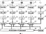
图1是一个超声波成象装置的构成方框图;Fig. 1 is a block diagram of the composition of an ultrasonic imaging device;
图2是依据本发明原理构造的各接收通道处理器的原理方框图;Fig. 2 is the principle block diagram of each receiving channel processor constructed according to the principles of the present invention;
图3是起始延时逻辑的原理方框图;Fig. 3 is the principle block diagram of initial delay logic;
图4是动态聚焦逻辑单元的原理方框图;Fig. 4 is a schematic block diagram of a dynamic focus logic unit;
图5是插值变迹系数产生逻辑的原理方框图;Fig. 5 is a principle block diagram of interpolation apodization coefficient generation logic;
图6是数据存储器及其读控制器的原理方框图。Fig. 6 is a schematic block diagram of the data memory and its read controller.
具体实施方式 Detailed ways
为了更好地全面理解本发明,下面将结合本发明的一个优选实例和附图进行详细的说明。In order to understand the present invention better and comprehensively, a detailed description will be given below in conjunction with a preferred example of the present invention and accompanying drawings.
图1是一个超声波成象装置的构成方框图,该超声波成象装置使用多阵元探头,因此波束合成器包含多个信号处理通道。来自目标的回波由探头的各阵元接收,每个阵元连接到不同的接收通道。在每个接收通道中,来自探头阵元的信号被放大,然后以统一的速率数字化。为了简化描述,假设探头阵元只有四个,但它也可更大些。四个发射器10至13产生常规的驱动脉冲,激励探头阵元向受测试的机体组织发射超声波,之后,这些阵元又接收从受测试的机体组织中反射回来的超声波。在并行接收信道2至5,各阵元接收到的回波分别由放大器14至17放大,然后分别由A/D变换器20至23以统一的速率进行数字化。数字化后的回波信号进入各通道的处理器,在这里完成聚焦延时、加权与串行求和。处理器27的输出是波束合成信号,该信号由检测器6检测。为了在显示器9上显示数据,必须用数字扫描变换器7将回波数据转换为视频信号。系统所有的控制都由控制器8产生的控制信号来执行。FIG. 1 is a block diagram of an ultrasonic imaging device. The ultrasonic imaging device uses a multi-element probe, so the beamformer includes multiple signal processing channels. Echoes from the target are received by the transducer's array elements, each of which is connected to a different receive channel. In each receive channel, the signal from the probe elements is amplified and then digitized at a uniform rate. To simplify the description, it is assumed that there are only four probe elements, but it could be larger. The four
本发明的关键之处在于根据发明目的,对处理器的结构进行改进。图2是依据本发明原理构造的各接收通道处理器的原理方框图;所述处理器阵元包括:The key point of the invention is to improve the structure of the processor according to the purpose of the invention. Fig. 2 is the principle block diagram of each receiving channel processor constructed according to the principles of the present invention; the array element of the processor comprises:
具有FIFO结构的延时储存器30,用于提供信号接收处理通道的粗延时;A
线性插值器39,用于提供信号接收处理通道的细延时;A
动态聚焦32,用于向延时储存器30提供读使能控制,并提供细延迟代码;
起始延时31,用于控制延时储存器30的写使能,达到控制起始延时的目的;The
插值变迹系数产生器33,用于把细延迟代码映射为插值系数,并计算出变迹插值系数;The interpolation
线性插值器39的信号输入端口分别连接延时储存器30、动态聚焦32和插值变迹系数产生器33,其信号输出端经第一加法器38连接检测器6。The signal input port of the
所述线性插值器39包括顺序连接的第一乘法器35、第二加法器37以及第一锁存器34和第二乘法器36,第一锁存器34的输入端连接动态聚焦32,第一乘法器35和第二乘法器36的输入端连接插值变迹系数产生器33,第二乘法器36的输出端与第二加法器37连接。延时存储器30采用FIFO结构,其深度由所需的最大延时量决定,读写时钟CKO为射频采样时钟。延时存储器30与线性插值器39分别提供接收通道的粗延时与细延时,粗延时精度等于射频采样间隔T,细延时精度等于T/M,M由所需的延时精度决定,T的取值范围一般在40ns~25ns之间。在本例中M等于4。延时存储器的写使能由起始延时31提供,起始延时31根据各接收通道所需的起始粗延时控制延时存储器30的写使能,而各接收通道所需的起始细延时则由动态聚焦32给出。当所有接收通道的延时存储器都有数据样本写入的时候,动态聚焦32打开各通道延时存储器30的读使能,同时也打开第一锁存器34的时钟使能。动态聚焦32输出的细延时代码s1s2s3s4有五种可能状态:D0=0000,D1=1000,D2=0100,D3=0010,D4=0001,与线性插值系数a和b的关系是:s1s2s3s4=1000则a=1,b=0;s1s2s3s4=0100则a=3/4,b=1/4;s1s2s3s4=0010则a=2/4,b=2/4;s1s2s3s4=0001则a=1/4,b=3/4;s1s2s3s4=0000则a=1/4,b=3/4。在接收聚焦延时的动态调整过程中,细延时代码的五种可能状态按一种循环规律变化:D4变D3、D3变D2、D2变D1、D1变D0、D0变D4。假设当前细延时代码状态为D2=0100,当接收聚焦延时需要调整时,D2变为D1,插值系数由a=3/4、b=1/4变为a=1、b=0,线性插值器的输出延时增加一个细延时单位T/M;当接收聚焦延时再需要调整时,D1变为D0,但D0状态只持续一个射频采样周期,然后变为D4稳定下来,直到下一次调整接收聚焦延时。所以称D0为暂态,而称D1至D4为稳态。D0状态与D4状态的插值系数是一样的,但在D0状态,延时FIFO停读一拍,第一锁存器34也停工一拍。插值变迹系数产生单元33的作用是把细延时代码映射为插值系数,并完成插值系数与通道加权系数的合并。第一加法器38是通道间串行求和链上的一个环节。Described
所述起始延时31包括起始延时计数器40、第二锁存器41、第一或门42和第一与门43;第二锁存器41的输入输出端分别连接数据存储器及其读控制器28和起始延时计数器40,第一与门43的输入输出端分别连接控制器8、起始延时计数器40和延时储存器30(图3);起始延时计数器40是可装载计数器,它在接收期开始前装载起始粗延时数据,在接收期开始后以射频采样率计数,计满时开启延时储存器30的写使能。一个脉冲周期分成几个时段,首先是参数预置期,其次是脉冲发射期,然后是回波接收期,最后是延时FIFO的移位输出期。在参数预置期,第二锁存器41锁存本通道的起始粗延时数据;在脉冲发射期,起始粗延时数据加载计数器40;在回波接收器,计数器40开始计数,计满时打开延时FIFO的写使能,同时关闭计数器40的计数使能。Described
所述动态聚焦32包括可装载循环移位寄存器50、第三锁存器51、第四锁存器52、第五锁存器53、第十锁存器55、第十一锁存器58和第十二锁存器59、第二或门54、第三或门56和第二与门57;寄存器50的data输入端经第三锁存器51连接数据存储器及其读控制器28,其en输入端经第二或门54、第五锁存器53、第四锁存器52连接数据存储器及其读控制器28,其load输入端直接连接控制器8(图4);它在接收期开始前装载起始细延时数据,在接收进程中通过循环左移对起始延时进行动态的调整,以达到动态聚焦的目的。动态聚焦32的核心是一个5位的循环移位寄存器50。在参数预置期,第三锁存器51锁存本通道的起始细延时代码,起始细延时代码是四个稳态中的一个;在脉冲发射期,起始细延时代码加载循环移位寄存器的右四位。循环移位寄存器的右四位输出是细延时代码s1s2s3s4,它们的或输出在延时FIFO的移位输出期用来控制延时FIFO的读使能。在延时FIFO的移位输出期,第四锁存器52锁存聚焦延时动态调整数据,聚焦延时动态调整数据是1bit的数据流。在第四锁存器52锁存到一个高电平的时候,第五锁存器53把这个高电平变为一个相移脉冲,相移脉冲是宽度为射频采样周期的正脉冲,相移脉冲为第四锁存器52清零,也使循环移位寄存器左移一位。当循环移位寄存器中的1移到最左边时,会紧接一次移位,使细延时代码的D0状态只持续一个射频采样周期。The
所述插值变迹系数产生器33包括组合逻辑60、第六锁存器61、第七锁存器62、第八锁存器65和第九锁存器66、第三乘法器63和第四乘法器64;组合逻辑60把细延时代码映射为线性插值器的两个系数a和b,第六锁存器61和第七锁存器62构成两级变迹系数锁存器,在接收进程中变迹系数分时锁存到各通道第一级的变迹系数锁存器中,然后在同一时刻更新第二级锁存器的内容,变迹系数在第三乘法器63和第四乘法器64中分别与插值系数a和b相乘,最后由第八锁存器65和第九锁存器66分别输出变迹插值系数A和B,以达到动态变迹的目的(图5)。The interpolation
所述数据存储器及其读控制器28包括延时数据存储器70和变迹数据存储器71以及两个数据读控制器;延时数据存储器70和变迹数据存储器71分别存储不同接收通道的聚焦延时数据和动态变迹数据。在延时数据存储器70中包含起始延时数据和动态调整数据,延时数据存储器70和变迹数据存储器71各有自己的读控制器。延时数据读控制器72提供给延时数据存储器70读地址,变迹数据读控制器73提供给变迹数据存储器71读地址,并给出各通道变迹数据的锁存脉冲(图6)。延时数据存储器70、变迹数据存储器71分别存储四个接收通道的聚焦延时数据和动态变迹数据。在延时数据存储器中包含起始延时数据和动态调整数据。延时数据存储器70、变迹数据存储器71各有自己的读控制器。延时数据读控制器提供给延时数据存储器70读地址,给出动态调整数据锁存脉冲CK1,还给出8个起始延时数据锁存脉冲,其中4个用来锁存四接收通道的起始粗延时数据,另4个则用来锁存四接收通道的起始细延时数据。变迹数据读控制器提供给变迹数据存储器71读地址,并给出四通道变迹数据的锁存脉冲。The data memory and its
Claims (10)
Priority Applications (1)
| Application Number | Priority Date | Filing Date | Title |
|---|---|---|---|
| CNB021346321ACN1307427C (en) | 2002-08-28 | 2002-08-28 | Beam synthesizer and synthetic method based on linear interpolation |
Applications Claiming Priority (1)
| Application Number | Priority Date | Filing Date | Title |
|---|---|---|---|
| CNB021346321ACN1307427C (en) | 2002-08-28 | 2002-08-28 | Beam synthesizer and synthetic method based on linear interpolation |
Publications (2)
| Publication Number | Publication Date |
|---|---|
| CN1439898A CN1439898A (en) | 2003-09-03 |
| CN1307427Ctrue CN1307427C (en) | 2007-03-28 |
Family
ID=27793405
Family Applications (1)
| Application Number | Title | Priority Date | Filing Date |
|---|---|---|---|
| CNB021346321AExpired - Fee RelatedCN1307427C (en) | 2002-08-28 | 2002-08-28 | Beam synthesizer and synthetic method based on linear interpolation |
Country Status (1)
| Country | Link |
|---|---|
| CN (1) | CN1307427C (en) |
Families Citing this family (10)
| Publication number | Priority date | Publication date | Assignee | Title |
|---|---|---|---|---|
| CN1310038C (en)* | 2003-12-30 | 2007-04-11 | 中国科学院声学研究所 | Synthetic aperture and delayed addition imaging method |
| CN100337595C (en)* | 2004-06-18 | 2007-09-19 | 深圳迈瑞生物医疗电子股份有限公司 | Beam composition method and device based on null aim interpolation |
| CN101373181B (en)* | 2007-08-24 | 2012-03-21 | 深圳迈瑞生物医疗电子股份有限公司 | Method and apparatus for calculating point-to-point trace-changing coefficient in real time |
| CN101303407B (en)* | 2008-05-28 | 2011-03-02 | 哈尔滨工业大学 | Thin film type infrared-radar beam synthesizer |
| CN101849838B (en)* | 2009-03-30 | 2013-10-16 | 深圳迈瑞生物医疗电子股份有限公司 | Method and device for eliminating transient state in ultrasonic system |
| CN101865998A (en)* | 2010-05-19 | 2010-10-20 | 深圳市蓝韵实业有限公司 | Delay parameter real-time computation and production line type multi-beam synthesis method |
| CN104251886B (en)* | 2013-06-26 | 2016-12-28 | 北京时代之峰科技有限公司 | The method and device that in a kind of ultrasonic examination, dynamic subdivision postpones |
| CN104914440B (en)* | 2015-06-23 | 2017-06-16 | 重庆大学 | A kind of compressed sensing ultrasonic beam synthetic method for merging dynamic aperture |
| JP6038259B1 (en)* | 2015-10-20 | 2016-12-07 | 株式会社日立製作所 | Ultrasonic diagnostic equipment |
| CN109549669A (en)* | 2018-12-05 | 2019-04-02 | 余姚市华耀工具科技有限公司 | Oriented detection formula B ultrasound imager |
Citations (6)
| Publication number | Priority date | Publication date | Assignee | Title |
|---|---|---|---|---|
| US5345426A (en)* | 1993-05-12 | 1994-09-06 | Hewlett-Packard Company | Delay interpolator for digital phased array ultrasound beamformers |
| US5544128A (en)* | 1994-07-05 | 1996-08-06 | Siemens Medical Systems, Inc. | Multi-beam digital beamforming method and apparatus |
| CN1212146A (en)* | 1997-05-27 | 1999-03-31 | 索诺塞特公司 | Hand held ultrasonic diagnostic instrument with digital beamformer |
| CN2387863Y (en)* | 1999-07-19 | 2000-07-19 | 开曼迈瑞医疗电子(深圳)有限公司 | All-number real-time B-mode ultrasonic receiving dynamic apodization beam synthetic device |
| CN1286963A (en)* | 1999-09-08 | 2001-03-14 | 开曼迈瑞医疗电子(深圳)有限公司 | Full-digital wave beam synthesizer for B-mode ultrasonic diagnostic equipment |
| US6315723B1 (en)* | 1999-10-08 | 2001-11-13 | Atl Ultrasound | Ultrasonic diagnostic imaging system with synthesized transmit focus |
- 2002
- 2002-08-28CNCNB021346321Apatent/CN1307427C/ennot_activeExpired - Fee Related
Patent Citations (6)
| Publication number | Priority date | Publication date | Assignee | Title |
|---|---|---|---|---|
| US5345426A (en)* | 1993-05-12 | 1994-09-06 | Hewlett-Packard Company | Delay interpolator for digital phased array ultrasound beamformers |
| US5544128A (en)* | 1994-07-05 | 1996-08-06 | Siemens Medical Systems, Inc. | Multi-beam digital beamforming method and apparatus |
| CN1212146A (en)* | 1997-05-27 | 1999-03-31 | 索诺塞特公司 | Hand held ultrasonic diagnostic instrument with digital beamformer |
| CN2387863Y (en)* | 1999-07-19 | 2000-07-19 | 开曼迈瑞医疗电子(深圳)有限公司 | All-number real-time B-mode ultrasonic receiving dynamic apodization beam synthetic device |
| CN1286963A (en)* | 1999-09-08 | 2001-03-14 | 开曼迈瑞医疗电子(深圳)有限公司 | Full-digital wave beam synthesizer for B-mode ultrasonic diagnostic equipment |
| US6315723B1 (en)* | 1999-10-08 | 2001-11-13 | Atl Ultrasound | Ultrasonic diagnostic imaging system with synthesized transmit focus |
Also Published As
| Publication number | Publication date |
|---|---|
| CN1439898A (en) | 2003-09-03 |
Similar Documents
| Publication | Publication Date | Title |
|---|---|---|
| JP3645938B2 (en) | Beam shaper and method of generating beam shaper signals | |
| US5469851A (en) | Time multiplexed digital ultrasound beamformer | |
| US5369624A (en) | Digital beamformer having multi-phase parallel processing | |
| US20240061107A1 (en) | Ultrasound probe with multiline digital microbeamformer | |
| CN101209211B (en) | Synthesis method and device for digitalization ultrasonic beam with adjustable receiver aperture | |
| CN1307427C (en) | Beam synthesizer and synthetic method based on linear interpolation | |
| US11353582B2 (en) | Ultrasound probe with low frequency, low voltage digital microbeamformer | |
| US11627940B2 (en) | Ultrasound probe with digital microbeamformer using fir filters with no multipliers | |
| TW201905490A (en) | Web format digital microwave beamforming for ultrasonic applications | |
| JPH08505556A (en) | Partial beam formation | |
| US11771403B2 (en) | Ultrasound probe with thirty-two channel digital microbeamformer | |
| US11937982B2 (en) | 2D array ultrasound probe with 3 watt digital microbeamformer | |
| US11630193B2 (en) | Ultrasound probe with digital microbeamformer having integrated circuits fabricated with different manufacturing processes | |
| Song et al. | Ultrasonic dynamic focusing using an analog FIFO and asynchronous sampling | |
| Guo et al. | A 1.2-mW/channel pitch-matched transceiver ASIC employing a boxcar-integration-based RX micro-beamformer for high-resolution 3-D ultrasound imaging | |
| JP2010063875A (en) | Delay adjustment module and ultrasonic receiving beam forming apparatus | |
| WO2018041636A1 (en) | Ultrasound probe with multiline digital microbeamformer | |
| CN100337595C (en) | Beam composition method and device based on null aim interpolation | |
| Camacho et al. | A strict-time distributed architecture for digital beamforming of ultrasound signals | |
| JPH08173431A (en) | Ultrasonic diagnostic device | |
| JP6038259B1 (en) | Ultrasonic diagnostic equipment | |
| JPH04161878A (en) | variable delay circuit | |
| JP2002143162A (en) | Ultrasound diagnostic equipment | |
| JPH05137717A (en) | Beamformer of ultrasonic diagnostic equipment | |
| JPH05137720A (en) | Beamformer of ultrasonic diagnostic equipment |
Legal Events
| Date | Code | Title | Description |
|---|---|---|---|
| C06 | Publication | ||
| PB01 | Publication | ||
| C10 | Entry into substantive examination | ||
| SE01 | Entry into force of request for substantive examination | ||
| C14 | Grant of patent or utility model | ||
| GR01 | Patent grant | ||
| CF01 | Termination of patent right due to non-payment of annual fee | Granted publication date:20070328 Termination date:20140828 | |
| EXPY | Termination of patent right or utility model |