CN1305639A - Fabrication of gallium nitride semiconductor layers by lateral growth from treach sidewalls - Google Patents
Fabrication of gallium nitride semiconductor layers by lateral growth from treach sidewallsDownload PDFInfo
- Publication number
- CN1305639A CN1305639ACN99807244ACN99807244ACN1305639ACN 1305639 ACN1305639 ACN 1305639ACN 99807244 ACN99807244 ACN 99807244ACN 99807244 ACN99807244 ACN 99807244ACN 1305639 ACN1305639 ACN 1305639A
- Authority
- CN
- China
- Prior art keywords
- gallium nitride
- lateral
- layer
- underlying
- sidewalls
- Prior art date
- Legal status (The legal status is an assumption and is not a legal conclusion. Google has not performed a legal analysis and makes no representation as to the accuracy of the status listed.)
- Granted
Links
Images


Classifications
- H—ELECTRICITY
- H01—ELECTRIC ELEMENTS
- H01L—SEMICONDUCTOR DEVICES NOT COVERED BY CLASS H10
- H01L21/00—Processes or apparatus adapted for the manufacture or treatment of semiconductor or solid state devices or of parts thereof
- H01L21/02—Manufacture or treatment of semiconductor devices or of parts thereof
- H01L21/04—Manufacture or treatment of semiconductor devices or of parts thereof the devices having potential barriers, e.g. a PN junction, depletion layer or carrier concentration layer
- H01L21/18—Manufacture or treatment of semiconductor devices or of parts thereof the devices having potential barriers, e.g. a PN junction, depletion layer or carrier concentration layer the devices having semiconductor bodies comprising elements of Group IV of the Periodic Table or AIIIBV compounds with or without impurities, e.g. doping materials
- H—ELECTRICITY
- H01—ELECTRIC ELEMENTS
- H01L—SEMICONDUCTOR DEVICES NOT COVERED BY CLASS H10
- H01L21/00—Processes or apparatus adapted for the manufacture or treatment of semiconductor or solid state devices or of parts thereof
- H01L21/02—Manufacture or treatment of semiconductor devices or of parts thereof
- H01L21/02104—Forming layers
- H01L21/02365—Forming inorganic semiconducting materials on a substrate
- H01L21/02612—Formation types
- H01L21/02617—Deposition types
- H01L21/02636—Selective deposition, e.g. simultaneous growth of mono- and non-monocrystalline semiconductor materials
- H01L21/02647—Lateral overgrowth
- H01L21/0265—Pendeoepitaxy
- H—ELECTRICITY
- H01—ELECTRIC ELEMENTS
- H01L—SEMICONDUCTOR DEVICES NOT COVERED BY CLASS H10
- H01L21/00—Processes or apparatus adapted for the manufacture or treatment of semiconductor or solid state devices or of parts thereof
- H01L21/02—Manufacture or treatment of semiconductor devices or of parts thereof
- H01L21/02104—Forming layers
- H01L21/02365—Forming inorganic semiconducting materials on a substrate
- H01L21/02367—Substrates
- H01L21/0237—Materials
- H01L21/02373—Group 14 semiconducting materials
- H01L21/02378—Silicon carbide
- H—ELECTRICITY
- H01—ELECTRIC ELEMENTS
- H01L—SEMICONDUCTOR DEVICES NOT COVERED BY CLASS H10
- H01L21/00—Processes or apparatus adapted for the manufacture or treatment of semiconductor or solid state devices or of parts thereof
- H01L21/02—Manufacture or treatment of semiconductor devices or of parts thereof
- H01L21/02104—Forming layers
- H01L21/02365—Forming inorganic semiconducting materials on a substrate
- H01L21/02436—Intermediate layers between substrates and deposited layers
- H01L21/02439—Materials
- H01L21/02455—Group 13/15 materials
- H01L21/02458—Nitrides
- H—ELECTRICITY
- H01—ELECTRIC ELEMENTS
- H01L—SEMICONDUCTOR DEVICES NOT COVERED BY CLASS H10
- H01L21/00—Processes or apparatus adapted for the manufacture or treatment of semiconductor or solid state devices or of parts thereof
- H01L21/02—Manufacture or treatment of semiconductor devices or of parts thereof
- H01L21/02104—Forming layers
- H01L21/02365—Forming inorganic semiconducting materials on a substrate
- H01L21/02518—Deposited layers
- H01L21/02521—Materials
- H01L21/02538—Group 13/15 materials
- H01L21/0254—Nitrides
- H—ELECTRICITY
- H01—ELECTRIC ELEMENTS
- H01L—SEMICONDUCTOR DEVICES NOT COVERED BY CLASS H10
- H01L21/00—Processes or apparatus adapted for the manufacture or treatment of semiconductor or solid state devices or of parts thereof
- H01L21/02—Manufacture or treatment of semiconductor devices or of parts thereof
- H01L21/02104—Forming layers
- H01L21/02365—Forming inorganic semiconducting materials on a substrate
- H01L21/02612—Formation types
- H01L21/02617—Deposition types
- H01L21/0262—Reduction or decomposition of gaseous compounds, e.g. CVD
- H—ELECTRICITY
- H01—ELECTRIC ELEMENTS
- H01L—SEMICONDUCTOR DEVICES NOT COVERED BY CLASS H10
- H01L21/00—Processes or apparatus adapted for the manufacture or treatment of semiconductor or solid state devices or of parts thereof
- H01L21/02—Manufacture or treatment of semiconductor devices or of parts thereof
- H01L21/02104—Forming layers
- H01L21/02365—Forming inorganic semiconducting materials on a substrate
- H01L21/02612—Formation types
- H01L21/02617—Deposition types
- H01L21/02636—Selective deposition, e.g. simultaneous growth of mono- and non-monocrystalline semiconductor materials
- H01L21/02639—Preparation of substrate for selective deposition
- H—ELECTRICITY
- H01—ELECTRIC ELEMENTS
- H01L—SEMICONDUCTOR DEVICES NOT COVERED BY CLASS H10
- H01L21/00—Processes or apparatus adapted for the manufacture or treatment of semiconductor or solid state devices or of parts thereof
- H01L21/02—Manufacture or treatment of semiconductor devices or of parts thereof
- H01L21/02104—Forming layers
- H01L21/02365—Forming inorganic semiconducting materials on a substrate
- H01L21/02612—Formation types
- H01L21/02617—Deposition types
- H01L21/02636—Selective deposition, e.g. simultaneous growth of mono- and non-monocrystalline semiconductor materials
- H01L21/02647—Lateral overgrowth
- H—ELECTRICITY
- H01—ELECTRIC ELEMENTS
- H01S—DEVICES USING THE PROCESS OF LIGHT AMPLIFICATION BY STIMULATED EMISSION OF RADIATION [LASER] TO AMPLIFY OR GENERATE LIGHT; DEVICES USING STIMULATED EMISSION OF ELECTROMAGNETIC RADIATION IN WAVE RANGES OTHER THAN OPTICAL
- H01S2304/00—Special growth methods for semiconductor lasers
- H01S2304/12—Pendeo epitaxial lateral overgrowth [ELOG], e.g. for growing GaN based blue laser diodes
- H—ELECTRICITY
- H01—ELECTRIC ELEMENTS
- H01S—DEVICES USING THE PROCESS OF LIGHT AMPLIFICATION BY STIMULATED EMISSION OF RADIATION [LASER] TO AMPLIFY OR GENERATE LIGHT; DEVICES USING STIMULATED EMISSION OF ELECTROMAGNETIC RADIATION IN WAVE RANGES OTHER THAN OPTICAL
- H01S5/00—Semiconductor lasers
- H01S5/02—Structural details or components not essential to laser action
- H01S5/0206—Substrates, e.g. growth, shape, material, removal or bonding
- H01S5/021—Silicon based substrates
Landscapes
- Engineering & Computer Science (AREA)
- Physics & Mathematics (AREA)
- Condensed Matter Physics & Semiconductors (AREA)
- General Physics & Mathematics (AREA)
- Manufacturing & Machinery (AREA)
- Computer Hardware Design (AREA)
- Microelectronics & Electronic Packaging (AREA)
- Power Engineering (AREA)
- Chemical & Material Sciences (AREA)
- Materials Engineering (AREA)
- Recrystallisation Techniques (AREA)
- Crystals, And After-Treatments Of Crystals (AREA)
Abstract
Translated fromChinese
Description
Translated fromChinese发明领域field of invention
本发明涉及到微电子器件和制造方法,尤其涉及到氮化镓半导体器件及其制造方法。The invention relates to a microelectronic device and a manufacturing method, in particular to a gallium nitride semiconductor device and a manufacturing method thereof.
发明背景Background of the invention
氮化镓正被广泛地研究用于微电子器件,这些微电子器件包括,但不局限于,晶体管、场发射器和光电子器件。可以理解的是,正如这里使用的那样,氮化镓还包括氮化镓的合金,如铝镓氮、铟镓氮和铝铟镓氮。Gallium nitride is being extensively studied for use in microelectronic devices including, but not limited to, transistors, field emitters, and optoelectronic devices. It will be appreciated that, as used herein, gallium nitride also includes alloys of gallium nitride, such as aluminum gallium nitride, indium gallium nitride, and aluminum indium gallium nitride.
在制造氮化镓基微电子器件时,一个主要问题是制造低缺陷密度的氮化镓半导体层。已知引起缺陷密度的一个原因是要在其上生长氮化镓层的衬底。相应地,尽管已经在蓝宝石衬底上生长了氮化镓层,但已知借助在自我形成于碳化硅衬底上的氮化铝缓冲层上生长氮化镓层来降低缺陷密度。虽然已有了这些进展,但所有进一步降低缺陷密度。When fabricating GaN-based microelectronic devices, a major problem is the fabrication of GaN semiconductor layers with low defect density. One known cause of defect density is the substrate on which the gallium nitride layer is to be grown. Accordingly, although a gallium nitride layer has been grown on a sapphire substrate, it is known to reduce the defect density by growing a gallium nitride layer on a self-formed aluminum nitride buffer layer on a silicon carbide substrate. Despite these advances, all have further reduced defect density.
还已知通过掩模中的窗口来制造氮化镓结构。例如,在制造场发射器阵列的过程中,已知在条形或圆形图案化的衬底上选择性地生长氮化镓。例如见Nam等人题为"利用金属有机气相外延的GaN/AlN/6H-SiC(0001)衬底上的GaN和Al0.2Ga0.8N选择性生长(Selective Growth of GaN and Al0.2Ga0.8N on GaN/AlN/6H-SiC(0001)Multilayer Substrates Via Organometallic Vapor PhaseEpitaxy)",Proceedings of the Materials Research Society,December 1996,以及"利用金属有机气相外延图形化的衬底上的GaN和Al0.2Ga0.8N的生长(Growth of GaN and Al0.2Ga0.8N on PatterenedSubstrates via Organometallic Vapor Phase Epitaxy)",JapaneseJournal of Applied Physics,Vol.36,Part 2,No.5A,May 1997,pp.L532-L535的文章。正如在这些文章中所公开的那样,在一定条件下,可能出现不希望的脊形生长或横向过生长。It is also known to fabricate gallium nitride structures through windows in masks. For example, in the fabrication of field emitter arrays, it is known to selectively grow gallium nitride on strip- or circularly patterned substrates. See, for example, Nam et al. entitled "Selective Growthof GaN and Al0.2 Ga0.8 N on GaN/AlN/6H-SiC (0001) Substrates byMetal -Organic Vapor Phase Epitaxy" GaN/AlN/6H-SiC (0001) Multilayer Substrates Via Organometallic Vapor Phase Epitaxy)", Proceedings of the Materials Research Society, December 1996, and "GaN and Al0.2 Ga0.8 N on Substrates Patterned by Metal-Organic Vapor Phase Epitaxy (Growth of GaN and Al0.2 Ga0.8 N on Patterned Substrates via Organometallic Vapor Phase Epitaxy)", Japanese Journal of Applied Physics, Vol.36, Part 2, No.5A, May 1997, pp.L532-L535. As disclosed in these articles, under certain conditions, undesired ridge growth or lateral overgrowth may occur.
发明概述Summary of the invention
因此,本发明的一个目的是提供制造氮化镓半导体层的改进了的方法以及这样制造的改进了的氮化镓层。It is therefore an object of the present invention to provide an improved method of manufacturing gallium nitride semiconductor layers and an improved gallium nitride layer thus manufactured.
本发明的另一个目的是提供能够制造具有低缺陷密度的氮化镓半导体层的方法以及这样制造的氮化镓半导体层。Another object of the present invention is to provide a method capable of manufacturing a gallium nitride semiconductor layer having a low defect density and the gallium nitride semiconductor layer thus manufactured.
根据本发明,借助于将一个下方氮化镓层的一个侧壁横向生长到该下方氮化镓层中的一个沟槽中,从而形成一个横向氮化镓层,而提供了这些和其它的目的。然后可以在这个横向氮化镓层中制作微电子器件。According to the present invention, these and other objects are provided by forming a lateral gallium nitride layer by laterally growing a sidewall of an underlying gallium nitride layer into a trench in the underlying gallium nitride layer . Microelectronic devices can then be fabricated in this lateral gallium nitride layer.
已经发现,根据本发明,在下方氮化镓层中,位错缺陷不再明显地从侧壁横向传播到沟槽中,致使横向氮化镓半导体层相对地无缺陷。在横向氮化镓层的生长过程中,无需掩蔽下方氮化镓层部分,就可以实现侧壁生长。It has been found that, in accordance with the present invention, in the underlying gallium nitride layer, dislocation defects no longer propagate significantly laterally from the sidewalls into the trench, rendering the lateral gallium nitride semiconductor layer relatively defect-free. During the growth of the lateral GaN layer, sidewall growth can be achieved without masking portions of the underlying GaN layer.
根据本发明的另一方面,下方氮化镓层的一对侧壁横向生长到位于这对侧壁之间的、下方氮化镓层中的沟槽中,直至生长的侧壁在这个沟槽中会合。可以用金属有机气相外延(MOVPE)来横向生长横向氮化镓半导体层。例如,可以用三乙基镓(TEG)和氨气(NH3)等前体,在1000-1100℃和45乇下横向生长横向氮化镓层。最好是13-39微摩尔/分钟的TEG和1500sccm的NH3与3000sccm的H2稀释剂组合使用。在1100℃的温度和45乇下使用26微摩尔/分钟的TEG、1500sccm的NH3和3000sccm的H2最佳。下方氮化镓层最好制作在诸如6H-SiC(0001)之类的衬底上,该类衬底其本身包括一个位于其上的诸如氮化铝之类的缓冲层。可以使用诸如蓝宝石之类的其它衬底和诸如低温氮化镓之类的其它缓冲层。也可以使用多衬底层和缓冲层。According to another aspect of the invention, a pair of sidewalls of the underlying gallium nitride layer is grown laterally into a trench in the underlying gallium nitride layer between the pair of sidewalls until the grown sidewalls are in the trench. rendezvous. The lateral gallium nitride semiconductor layer may be grown laterally using metal organic vapor phase epitaxy (MOVPE). For example, a lateral GaN layer can be grown laterally at 1000-1100° C. and 45 Torr using precursors such as triethylgallium (TEG) and ammonia gas (NH3 ). It is best to use 13-39 micromol/min of TEG and 1500 sccm ofNH3 in combination with 3000 sccm ofH2 diluent. It is optimal to use 26 micromol/min of TEG, 1500 sccm ofNH3 and 3000 sccm ofH2 at a temperature of 1100°C and 45 Torr. The underlying gallium nitride layer is preferably formed on a substrate such as 6H-SiC (0001), which itself includes a buffer layer such as aluminum nitride on top. Other substrates such as sapphire and other buffer layers such as low temperature gallium nitride can be used. Multiple substrate layers and buffer layers can also be used.
可以借助于在下方氮化镓层中制作沟槽来制作包括侧壁的下方氮化镓层,从而使沟槽包括侧壁。另外,可以借助于在下方氮化镓层上制作支柱来制作侧壁,支柱包括侧壁,并确定沟槽。最好制作一系列交替的沟槽和支柱,以形成多个侧壁。可以用选择性腐蚀、选择性外延生长、腐蚀与生长的组合,或其它技术制作沟槽和/或支柱。沟槽可以延伸到缓冲层中和到衬底中。The underlying gallium nitride layer comprising sidewalls may be formed by forming trenches in the underlying gallium nitride layer such that the trenches comprise sidewalls. Alternatively, the sidewalls can be formed by means of forming pillars on the underlying gallium nitride layer, the pillars comprising the sidewalls and defining the trenches. It is best to make a series of alternating trenches and struts to create multiple side walls. The trenches and/or pillars can be formed by selective etching, selective epitaxial growth, a combination of etching and growth, or other techniques. The trenches may extend into the buffer layer and into the substrate.
下方氮化镓层的侧壁横向生长进入沟槽中,从而形成一个缺陷密度低于下方氮化镓层的缺陷密度的横向氮化镓层。也可能出现一些纵向生长。在传播较低的缺陷密度时,横向生长的氮化镓层也会纵向生长。纵向生长也可以与横向生长同时发生。Sidewalls of the underlying GaN layer grow laterally into the trench, thereby forming a lateral GaN layer with a lower defect density than the underlying GaN layer. Some longitudinal growth may also occur. While propagating lower defect densities, laterally grown GaN layers also grow vertically. Vertical growth can also occur simultaneously with lateral growth.
借助于自横向氮化镓层生长一个第二氮化镓半导体层,可以进一步降低过生长的氮化镓半导体层的缺陷密度。在一个实施例中,用其中包括一个窗口阵列的掩模将横向氮化镓层掩蔽。横向氮化镓层通过这个窗口阵列生长到掩模上,从而形成一个过生长的氮化镓半导体层。在另一个实施例中,纵向生长横向氮化镓层。多个第二侧壁被制作在纵向生长的横向氮化镓层中,以确定多个第二沟槽。然后纵向生长的横向氮化镓层的多个第二侧壁横向生长进入多个第二沟槽中,从而形成一个第二横向氮化镓层。然后在这个氮化镓半导体层中制作微电子器件。如上所述,可以用金属有机气相外延来生长下方氮化镓层的多个侧壁。如上所述,可以借助于沟槽和/或支柱的腐蚀和/或选择性外延生长来生长第二侧壁。By growing a second gallium nitride semiconductor layer from the lateral gallium nitride layer, the defect density of the overgrown gallium nitride semiconductor layer can be further reduced. In one embodiment, the lateral gallium nitride layer is masked with a mask including an array of windows. A lateral GaN layer is grown through this array of windows onto the mask, forming an overgrown GaN semiconductor layer. In another embodiment, the lateral gallium nitride layers are grown vertically. A plurality of second sidewalls are formed in the vertically grown lateral GaN layer to define a plurality of second trenches. Then the plurality of second sidewalls of the vertically grown lateral GaN layer are laterally grown into the plurality of second trenches, thereby forming a second lateral GaN layer. Microelectronic devices are then fabricated in this gallium nitride semiconductor layer. As mentioned above, metal organic vapor phase epitaxy can be used to grow the multiple sidewalls of the underlying gallium nitride layer. As mentioned above, the second sidewall may be grown by means of etching and/or selective epitaxial growth of the trenches and/or pillars.
根据本发明的氮化镓半导体结构包括一个下方氮化镓层和一个横向氮化镓层,下方氮化镓层包括一个具有一个侧壁的沟槽,而横向氮化镓层从下方氮化镓层的侧壁延伸进入该沟槽中。一个纵向氮化镓层自横向氮化镓层延伸。多个微电子器件包括在该纵向氮化镓层中。可以提供一系列交替的沟槽和支柱,以便确定多个侧壁。下方氮化镓层包括一个预定的缺陷密度,而横向氮化镓层的缺陷密度低于此预定的缺陷密度。The gallium nitride semiconductor structure according to the present invention comprises a lower gallium nitride layer and a lateral gallium nitride layer, the lower gallium nitride layer comprises a trench with one sidewall, and the lateral gallium nitride layer extends from the lower gallium nitride layer The sidewalls of the layer extend into the trench. A vertical GaN layer extends from the lateral GaN layer. A plurality of microelectronic devices are included in the vertical gallium nitride layer. A series of alternating grooves and struts may be provided to define multiple sidewalls. The underlying GaN layer includes a predetermined defect density, and the lateral GaN layer has a defect density lower than the predetermined defect density.
根据本发明的氮化镓半导体结构的其它实施例包括一个掩模和一个纵向氮化镓层,该掩模位于横向氮化镓层上,并在其中包括一个窗口阵列,而该纵向氮化镓层通过窗口从横向氮化镓层延伸到掩模上的。或者,一个纵向氮化镓层自横向氮化镓层延伸,并且包括多个第二侧壁。一个第二横向氮化镓层从多个第二侧壁延伸。微电子器件包括在第二横向氮化镓层中。因此,可以生产低缺陷密度的氮化镓半导体层,从而能够生产高性能微电子器件。Other embodiments of gallium nitride semiconductor structures according to the present invention include a mask overlying the lateral gallium nitride layer and including an array of windows therein, and a vertical gallium nitride layer, the vertical gallium nitride layer Layers extend from the lateral GaN layer onto the mask through windows. Alternatively, a vertical GaN layer extends from the lateral GaN layer and includes a plurality of second sidewalls. A second lateral GaN layer extends from the second plurality of sidewalls. Microelectronic devices are included in the second lateral gallium nitride layer. As a result, gallium nitride semiconductor layers with low defect density can be produced, enabling the production of high-performance microelectronic devices.
附图的简要说明Brief description of the drawings
图1-5是根据本发明的中间制造步骤中氮化镓半导体结构第一实施例的横截面图。1-5 are cross-sectional views of a first embodiment of a gallium nitride semiconductor structure in an intermediate fabrication step according to the present invention.
图6-10是根据本发明的中间制造步骤中氮化镓半导体结构第二Fig. 6-10 is according to the intermediate fabrication step of the present invention in the gallium nitride semiconductor structure second
实施例的横截面图。Example cross-sectional view.
图11-15是根据本发明的中间制造步骤中氮化镓半导体结构第三11-15 are third gallium nitride semiconductor structures in intermediate manufacturing steps according to the present invention.
实施例的横截面图。Example cross-sectional view.
最佳实施例的详细描述Detailed description of the preferred embodiment
以下参照附图来更充分地描述本发明,附图示出了本发明的最佳实施例。但本发明可以许多不同的形式实施,因而不应该认为是局限于此处指出的各个实施例。提供这些实施例只是为了使本公开变得充分而完整,并将本发明的范围完全传达给本技术领域的熟练人员。为明晰起见,在附图中夸大了各个层和区域的厚度。各个图中相似的标号表示相似的元件。可以理解,当一个元件,如一个层、区域或衬底,被称为“在另一个元件上”或“到另一个元件上”时,它可以直接位于其它元件上,或者二者之间也可以存在插入的元件。而且,此处给出并描述的各个实施例也包括其互补导电类型的实施例。The present invention will be described more fully hereinafter with reference to the accompanying drawings, which show preferred embodiments of the invention. This invention may, however, be embodied in many different forms and should not be construed as limited to the embodiments set forth herein. Rather, these embodiments are provided so that this disclosure will be thorough and complete, and will fully convey the scope of the invention to those skilled in the art. In the drawings, the thicknesses of various layers and regions are exaggerated for clarity. Like numbers in the various figures indicate like elements. It will be understood that when an element such as a layer, region or substrate is referred to as being "on" or "on" another element, it can be directly on the other element or intervening elements may also be present. There may be intervening elements. Furthermore, each embodiment shown and described herein also includes its complementary conductivity type embodiment.
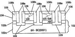
现参照图1-5描述根据本发明第一实施例的、制造氮化镓半导体结构的方法。如图1所示,在衬底102上生长下方氮化镓层104。衬底102可以包括一个6H-SiC(0001)衬底102a和一个氮化铝缓冲层102b。此处使用的结晶学命名习惯对于本技术领域熟练人员而言是熟知的,因而无需进一步描述。氮化镓层104的厚度可以在1.0-2.0微米之间,并可以在1000℃下,用26微摩尔/分钟的三乙基镓、1500sccm的氨和3000sccm的氢稀释剂,在冷壁垂直式、感应加热的金属有机气相外延系统中生长在高温(1100℃)氮化铝缓冲层102b上,而后者淀积在6H-SiC衬底102a上。在T.W.Weeks等人的题为"利用金属有机气相外延使用高温单晶AlN缓冲层在α(6H)-SiC(0001)上淀积GaN薄膜(GaN Thin Films Deposited Via Organometallic VaporPhase Epitaxy on α(6H)-SiC(0001)Using High-TemperatureMonocrystallic AlN Buffer Layers)",Applied Physics Letters,Vol.67,No.3,July 17,1995,pp.401-403的论文中,可以找到这一生长技术的其它细节,此处将其公开列为参考。可以使用有缓冲层或没有缓冲层的其它衬底。A method for fabricating a gallium nitride semiconductor structure according to a first embodiment of the present invention will now be described with reference to FIGS. 1-5 . As shown in FIG. 1 , an underlying
仍然参照图1,下方氮化镓层104包括其中的多个侧壁105。本技术领域的熟练人员可以理解,侧壁105可以想象为由亦可称为“台面”、“支座”或“柱”的多个分隔开的支柱106确定。侧壁105也可以想象为由亦称为“阱”的、下方氮化镓层104中的多个沟槽107确定。侧壁105还可以想象为由一系列交替的沟槽107和支柱106确定。可以理解,可以用选择性腐蚀和/或选择性外延生长和/或其它常规方法来制造确定侧壁105的支柱106和沟槽107。而且也可以理解,侧壁无需与衬底102正交,而是可以倾斜于衬底。最后还可以理解,虽然侧壁105以剖面形式示于图1中,但支柱106和沟槽107可以确定直的、V形的或其它形状的拉长的区域。如图1所示,沟槽107可以延伸进入缓冲层102b中和进入衬底102a中,致使后续的氮化镓生长择优地发生在侧壁105上,而不是在沟槽底部。在其它实施例中,根据,举例来说,沟槽的几何形状和氮化镓的横向对纵向生长速率,沟槽可以不延伸进入衬底102a中,而且也可以不延伸进入缓冲层102b中。Still referring to FIG. 1 , the underlying
现参照图2,横向生长下方氮化镓层104的侧壁105,以在沟槽107中形成横向氮化镓层108a。可以在1000-1100℃和45乇下获得氮化镓的横向生长。可以与3000sccm的H2稀释剂组合使用13-39微摩尔/分钟的TEG和1500sccm的NH3的前体。若制作氮化镓合金,则也可以使用,举例来说,额外的铝或铟的常规前体。如此处所使用的那样,术语“横向”意味着一个正交于侧壁105的方向。也可以理解,在始于侧壁105的横向生长过程中,支柱106上也可以发生一些纵向生长。如此处所使用的那样,术语“纵向”表示一个平行于侧壁105的方向。Referring now to FIG. 2 , the
现参照图3,横向氮化镓层108a的继续生长引起到下方氮化镓层104上,具体地讲是到支柱106上的纵向生长,从而形成纵向氮化镓层108b。纵向生长的生长条件可以保持为与结合图2所述的相同。同样如图3所示,可以在沟槽的底部发生进入沟槽107中的继续纵向生长。Referring now to FIG. 3 , continued growth of the
现参照图4,允许生长继续,直至横向生长前沿在沟槽107中会合于界面108c处,以便在沟槽中形成一个连续的氮化镓半导体层。总的生长时间可以是约60分钟。如图5所示,然后可以在横向氮化镓半导体层108a中制作微电子器件110。器件也可以制作在纵向氮化镓层108b中。Referring now to FIG. 4, growth is allowed to continue until the lateral growth fronts meet in
因此在图5中示出了根据本发明第一实施例的氮化镓半导体结构100。氮化镓结构100包括衬底102。衬底可以是蓝宝石或氮化镓或其它常规衬底。但衬底最好包括6H-SiC(0001)衬底102a和位于碳化硅衬底102a上的氮化铝缓冲层102b。氮化铝缓冲层102b的厚度可以是0.1微米。A gallium
对于本技术领域熟练人员来说,衬底102的制造是众所周知的,因此无需进一步描述。例如在授予Palmour的美国专利4865685中、在授予Davis等人的Re 34861中、在授予Kong等人的4912064中、以及授予Palmour等人的4946547中,描述了碳化硅衬底的制造,此处将这些公开列为参考。Fabrication of the
对着衬底102a、位于缓冲层102b上的下方氮化镓层104也包括在其中。下方氮化镓层104的厚度可以在大约1.0与2.0微米之间,并可以用金属有机气相外延(MOVPE)来制作。下方氮化镓层通常具有不希望有的相对高的缺陷密度。例如,大约108与1010cm-2之间的位错密度可以出现在下方氮化镓层中。这些高的缺陷密度可能来自缓冲层102b与下方氮化镓层104之间的晶格常数失配和/或其它原因。这些高的缺陷密度可以影响制作在下方氮化镓层104中的微电子器件的性能。Also included is an
仍然继续描述图5,下方氮化镓层104包括多个可能由多个支座106和/或多个沟槽107确定的侧壁105。如上所述,侧壁可以是倾斜的,并具有各种各样拉长的形状。Still continuing to describe FIG. 5 , the underlying
继续描述图5,横向氮化镓层108a从下方氮化镓层104的多个侧壁105延伸。可以在大约1000-1100℃和45乇下,用金属有机气相外延来制作横向氮化镓层108a。可以与3000sccm的H2稀释剂组合使用前体13-39微摩尔/分钟的三乙基镓(TEG)和1500sccm的氨(NH3)来制作横向氮化镓层108a。Continuing with the description of FIG. 5 , the
仍然继续描述图5,氮化镓半导体结构100还包括从支柱106纵向延伸的纵向氮化镓层108b。Still continuing to describe FIG. 5 , the
如图5所示,横向氮化镓层108a在界面108c处会合,从而在沟槽中形成一个连续的横向氮化镓半导体层108a。已经发现,下方氮化镓层104中的位错密度通常不以与从下方氮化镓层104纵向传播相同的密度从侧壁105横向传播。于是,横向氮化镓层108a可以具有相对低的缺陷密度,例如低于104cm-2。因此,横向氮化镓层108b可以形成器件质量的氮化镓半导体材料。于是,如图5所示,可以在横向氮化镓半导体层108a中制作微电子器件110。还可以理解,由于横向生长从侧壁105进行,故无需使用掩模来制造图5的氮化镓半导体结构100。As shown in FIG. 5, the
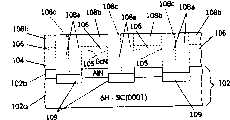
现参照图6-10来描述根据本发明的氮化镓半导体结构和制造方法的第二实施例。首先,按照如已参照图1-4所述的方法制造图4的氮化镓半导体结构。然后参照图6,用其中包括一个窗口阵列的掩模206掩蔽支柱106。此掩模可以包含厚度为1000埃的二氧化硅,并可以在410℃下用低压化学气相淀积进行淀积。可以使用其它的掩蔽材料。可以用标准的光刻技术制作掩模的图形,并在缓冲HF溶液中进行腐蚀。在一个实施例中,窗口的宽度为3微米,以3到40微米的距离平行延伸,其取向沿横向氮化镓层108a中的<1 100>方向。在进一步处理之前,可以将此结构浸入50%的盐酸(HCl)溶液中,以便清除表面氧化物。可以理解,虽然掩模206最好位于支柱106上,但也可以偏离支柱106。A second embodiment of the gallium nitride semiconductor structure and manufacturing method according to the present invention will now be described with reference to FIGS. 6-10 . First, the gallium nitride semiconductor structure of FIG. 4 is fabricated according to the method as already described with reference to FIGS. 1-4. Referring then to FIG. 6, the
现参照图7,通过窗口阵列生长横向氮化镓半导体层108a,从而在窗口中形成纵向氮化镓层208a。按照结合图2所述的方法可以获得氮化镓的生长。Referring now to FIG. 7, the lateral
可以理解,可以用二维生长来形成一个过生长的氮化镓半导体层。具体地讲,可以将掩模206图形化成包括一个沿诸如<1 1-00>和<11 2-0>的二个正交方向延伸的窗口阵列。于是,窗口能够形成一个正交条形图形的矩形。在此情况下,矩形各边的比率最好正比于{11 20}和{1 101}晶面生长速率的比率,例如1.4∶1的比率。窗口相对于<1 100>和<11 20>之类的方向可以是等边三角形。It will be appreciated that two-dimensional growth can be used to form an overgrown gallium nitride semiconductor layer. Specifically,
现参照图8,纵向氮化镓层208a的继续生长引起到掩模206上的横向生长,从而形成第二横向氮化镓层208b。可以将过生长的条件保持为如结合图7所述的那样。Referring now to FIG. 8, continued growth of the vertical
现参照图9,允许横向过生长继续,直至横向生长前沿在掩模206上的第二界面208c处会合,从而形成连续的过生长氮化镓半导体层208。总的生长时间可以是大约60分钟。如图10所示,然后可以在第二横向氮化镓层208b中制作微电子器件210。微电子器件也可以制作在纵向氮化镓层208a中。Referring now to FIG. 9 , the lateral overgrowth is allowed to continue until the lateral growth fronts meet at the second interface 208 c on the
因此,借助于提供第二横向生长层208b,甚至可以进一步降低原来出现在连续氮化镓半导体层108中的缺陷,从而在氮化镓半导体结构200中获得器件质量的氮化镓。Therefore, by providing the second
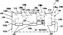
现参照图11-15来描述根据本发明的氮化镓半导体结构和制造方法的第三实施例。首先,如已结合图1-4所述那样制造图4的氮化镓半导体结构。然后制作多个第二侧壁305。可以借助于第二支柱306的选择性外延生长、借助于腐蚀第一支柱106中的第二沟槽307和/或它们的组合,来制作第二侧壁305。如上所述,第二侧壁305无需正交于衬底102,而可以是倾斜的。第二沟槽307无需直接在第一支柱106上,而是可以横向偏离支柱106。第二沟槽最好深一些,以便横向生长择优发生在侧壁305上而不是在第二沟槽306的底部。A third embodiment of the gallium nitride semiconductor structure and manufacturing method according to the present invention will now be described with reference to FIGS. 11-15 . First, the gallium nitride semiconductor structure of FIG. 4 is fabricated as already described in connection with FIGS. 1-4. A plurality of
现参照图12,横向生长第二支柱306和/或第二沟槽307的第二侧壁305,以便在第二沟槽307中形成第二横向氮化镓层308a。如上所述,可以在1000-1100℃和45乇下获得氮化镓的横向生长。可以与3000sccm的H2稀释剂组合使用前体13-39微摩尔/分钟的TEG和1500sccm的NH3。若制作氮化镓合金,则也可以使用例如铝或铟的额外常规前体。也可以理解,在始于第二侧壁305的横向生长过程中,第二支柱306上也可以发生一些纵向生长。Referring now to FIG. 12 , the
现参照图13,第二横向氮化镓层308a的继续生长引起到第二支柱306上的纵向生长,从而形成第二纵向氮化镓层308b。同样如图所示,也可能发生始于第二沟槽底部和始于第二支柱顶部的纵向生长。纵向生长的生长条件可以保持为结合图12所述的那样。Referring now to FIG. 13, continued growth of the second
现参照图14,允许生长继续,直至横向生长前沿在第二沟槽307中会合于第二界面308c处,从而形成第二连续氮化镓半导体层308。总的生长时间可以是大约60分钟。如图15所示,然后可以在第二连续氮化镓半导体层308中制作微电子器件310。Referring now to FIG. 14 , growth is allowed to continue until the lateral growth fronts meet in the
因此,可以制作根据本发明的氮化镓半导体结构300的第三实施例,而且无需为了确定横向生长而掩蔽氮化镓。而是可以利用始于第一和第二侧壁的横向生长。借助于执行二个分立的横向生长,可以显著降低缺陷密度。Thus, the third embodiment of the gallium nitride semiconductor structure 300 according to the invention can be fabricated without masking the gallium nitride in order to determine lateral growth. Instead, lateral growth from the first and second sidewalls can be utilized. By performing two separate lateral growths, the defect density can be significantly reduced.
下面提供有关本发明的方法和结构的其它讨论。第一和第二沟槽107和307以及掩模206中的窗口最好是下方氮化镓层104或第一横向氮化镓层108a上沿<11 20>和/或<1 100>方向择优延伸的矩形沟槽和窗口。对于沿<11 20>方向的沟槽和/或掩模窗口,可以获得具有(1 101)倾斜晶面和窄(0001)顶部晶面的截角三角形条形。沿<1 100>方向可以生长具有(0001)顶部晶面、(11 20)垂直侧面和(1 101)倾斜晶面的矩形条形。如果生长时间达到3分钟,则可以得到与取向无关的相似形貌。若继续生长,则条形发展成不同的形状。Additional discussion of the methods and structures of the present invention is provided below. The windows in the first and
横向生长量通常表现为强烈依赖于沟槽和/或掩模窗口的取向。通常,<1 100>取向的沟槽和/或掩模窗口的横向生长速率远快于沿<11 20>的速率。因此,将沟槽和/或掩模窗口定向成沿下方氮化镓层104或第一横向氮化镓层108a的<1 100>方向延伸为最佳。The amount of lateral growth generally appears to be strongly dependent on the orientation of the trench and/or mask window. Usually, <1 The lateral growth rate of trenches and/or mask windows in the 100> orientation is much faster than that along the <11 20> rate. Accordingly, the trenches and/or mask windows are oriented along <1 100> direction extension is the best.
作为沟槽和/或掩模窗口取向的函数,不同的形貌发展看来与氮化镓结构中结晶面的稳定性有关。沿<11 20>取向的沟槽和/或掩模窗口可以具有宽的(1 100)倾斜晶面以及一个非常窄的(0001)顶部晶面,或者没有后者,这取决于生长条件。这可能是因为(1 101)是氮化镓纤锌矿晶体结构中最稳定的面,且此面的生长速率低于其它面的生长速率。<1 100>取向的沟槽和/或掩模窗口的{1 101}面可以是波浪形的,这意味着存在一个以上的密勒指数。看来,在淀积过程中出现了选定的{1 101}面的竞争生长,它使这些面变得不稳定,并且相对于沿<11 20>取向的沟槽和/或掩模窗口的(1 101)的生长速率,它们的生长速率提高了。Different topographical developments appear to be related to the stability of crystallographic planes in GaN structures as a function of trench and/or mask window orientation. Edge <11 20> oriented trenches and/or mask windows can have wide (1 100) tilted crystal planes with a very narrow (0001) top crystal plane, or without the latter, depending on the growth conditions. This may be because (1 101) is the most stable plane in the GaN wurtzite crystal structure, and the growth rate of this plane is lower than that of other planes. <1 100> oriented trenches and/or mask windows of {1 101} Surfaces can be wavy, which means that there is more than one Miller index. It appears that during the deposition a selected {1 101} faces, which destabilizes these faces and is relatively 20> orientation of trenches and/or mask windows (1 101), their growth rate was increased.
从沿<1 100>取向的沟槽和/或掩模窗口选择性地生长的氮化镓层的形貌通常也强烈地表现为生长温度的函数。在1000℃下生长的层可以具有截角三角形形状。随着生长温度的提高,这一形貌可以逐渐地改变为矩形剖面。这种形貌变化可以归因于随着生长温度的提高,镓粒子的扩散系数随之增大,从而使之沿(0001)顶面到{1 101}面的流量增大。这可能导致(0001)面生长速率的降低和{1 101}面生长速率的提高。在二氧化硅上的砷化镓选择性生长中,也观察到了这种现象。因此,1100℃的温度看来是最佳的。from edge<1 The topography of GaN layers selectively grown with 100>-oriented trenches and/or mask windows is also generally a strong function of growth temperature. Layers grown at 1000°C may have a truncated triangular shape. This morphology can gradually change to a rectangular cross-section as the growth temperature increases. This morphological change can be attributed to the increase of the diffusion coefficient of gallium particles with the increase of growth temperature, which makes it along the (0001) top surface to {1 101} surface flow increases. This may lead to a decrease in the growth rate of the (0001) plane and {1 101} The improvement of surface growth rate. This phenomenon has also been observed in the selective growth of gallium arsenide on silicon dioxide. Therefore, a temperature of 1100°C appears to be optimum.
氮化镓区的形貌发展还表现出对TEG流速的依赖。TEG供应的增大通常使沿横向和纵向的生长速率都增大。但横向/纵向生长速率的比率从TEG流速为13微摩尔/分钟时的1.7降低到39微摩尔/分钟时的0.86。TEG流速对沿<0001>的生长速率相对于<11 20>生长速率的这一增大了的影响,可能与所用的、其中反应气体纵向且垂直于衬底流动的反应器有关。表面上镓粒子浓度的显著增大可以显著地阻碍其扩散到{1 101}面,致使(0001)面上更容易发生化学吸附和氮化镓生长。The morphology development of the GaN region also exhibits a dependence on the TEG flow rate. An increase in TEG supply generally increases the growth rate in both the transverse and longitudinal directions. But the ratio of lateral/vertical growth rate decreased from 1.7 at TEG flow rate of 13 μmol/min to 0.86 at 39 μmol/min. Effect of TEG flow rate on growth rate along <0001> relative to <11 20> This increased influence on the growth rate may be related to the reactor used in which the reactant gases flow longitudinally and perpendicularly to the substrate. A significant increase in the concentration of gallium particles on the surface can significantly hinder its diffusion into {1 101} plane, which makes the (0001) plane more prone to chemisorption and GaN growth.
用宽3微米、间距7微米、并沿<1 100>取向的沟槽和/或掩模窗口,在1100℃和26微摩尔/分钟的TEG流速下,可以获得厚度为2微米的连续氮化镓半导体层。此连续氮化镓半导体层可以包括二个生长前沿会合时形成的表面下的孔穴。使用会使具有垂直{11 20}侧晶面的矩形沟槽和/或掩模窗口发展的横向生长条件,最有可能出现这种孔穴。Use a width of 3 microns, a pitch of 7 microns, and an edge <1 100>-oriented trenches and/or mask windows, at 1100°C and a TEG flow rate of 26 micromol/min, a continuous gallium nitride semiconductor layer with a thickness of 2 microns can be obtained. The continuous gallium nitride semiconductor layer may include a subsurface cavity formed when two growth fronts meet. Using would make a vertical {11 Such voids are most likely to occur under lateral growth conditions where rectangular trenches and/or mask windows develop on the 20} side facets.
连续的氮化镓半导体层可以具有微观平坦且无坑的表面。横向生长的氮化镓层的表面可以包括台阶结构,其平均台阶高度为0.32nm。这一台阶结构可能与横向生长的氮化镓有关,因为它通常不包括在仅仅生长在氮化铝缓冲层上的更大面积的膜中。平均RMS粗糙度值可以相似于从下方氮化镓层104得到的值。The continuous gallium nitride semiconductor layer can have a microscopically flat and pit-free surface. The surface of the laterally grown gallium nitride layer may include a stepped structure with an average step height of 0.32 nm. This stepped structure may be relevant to the laterally grown GaN, since it is usually not included in larger-area films grown only on the AlN buffer layer. The average RMS roughness value may be similar to that obtained from the underlying
起源于下方氮化镓层104和缓冲层102b之间界面的针孔位错,看来传播到了下方氮化镓层104的上表面。这些区域内的位错密度约为109cm-2。相反,针孔位错(threading dislocation)看来不容易横向传播。而且横向氮化镓区域108a和308a中仅仅包含很少的位错。通过垂直针孔位错在再生长区域中弯曲90度之后的延伸,可以平行于(0001)面形成这些少量位错。这些位错看来不传播到过生长的氮化镓层的上表面。Pinhole dislocations originating at the interface between the
正如所述,选择性地生长的氮化镓层的形成机制是横向外延。此机制的二个主要阶段是纵向生长和横向生长。在通过掩模的纵向生长过程中,显然是由于镓原子在氮化镓表面上的附着系数s(s=1)比在掩模上的(s<<1)大得多,而使淀积的氮化镓在掩模窗口中比在掩模上更容易选择性地生长。由于SiO2键合强度为799.6千焦/摩尔,比Si-N(439千焦/摩尔)、Ga-N(103千焦/摩尔)和Ga-O(353.6千焦/摩尔)大得多,故Ga或N原子键合到掩模表面的数量和时间都不应当轻易在达到足以形成氮化镓核的程度。它们可能或者蒸发,或者沿掩模表面扩散到掩模窗口中或到已经形成的纵向氮化镓表面。在横向生长过程中,氮化镓同时纵向和横向生长。As mentioned, the formation mechanism of the selectively grown GaN layer is lateral epitaxy. The two main phases of this mechanism are longitudinal growth and lateral growth. During the vertical growth process through the mask, it is obvious that the adhesion coefficient s (s=1) of gallium atoms on the surface of gallium nitride is much larger than that on the mask (s<<1), so that the deposition GaN can be selectively grown more easily in the mask window than on the mask. Since the bonding strength ofSiO2 is 799.6 kJ/mol, which is much larger than that of Si-N (439 kJ/mol), Ga-N (103 kJ/mol) and Ga-O (353.6 kJ/mol), Therefore, the number and time of Ga or N atoms bonding to the mask surface should not be easily reached to a sufficient degree to form GaN nuclei. They may either evaporate or diffuse along the mask surface into the mask window or onto the already formed vertical GaN surface. During lateral growth, GaN grows both vertically and laterally.
在氮化镓的选择性生长中,镓和氮在氮化镓表面上的扩散可以起作用。材料的主要来源看来来自气相。TEG流速的增大引起(0001)顶部晶面的生长速率的发展快于(1 101)侧晶面,从而控制了横向生长的这一事实可以证明这一点。In the selective growth of GaN, the diffusion of gallium and nitrogen on the GaN surface can play a role. The major source of material appears to be from the gas phase. The increase of the TEG flow rate caused the growth rate of the (0001) top crystal face to develop faster than that of the (1 101) side facets, thus controlling the lateral growth can be proved by this fact.
横向生长的氮化镓与下方掩模的键合足够强,以致在冷却时它通常不会剥离。但由于冷却时产生的热应力,可能发生SiO2掩模中的横向破裂。SiO2在1050℃下的粘度(p)约为1015.5泊,这比体非晶体材料中在大约6小时内释放应力的应变点(大约1014.5泊)大一个数量级。于是,SiO2掩模在冷却时可以提供有限的柔量。由于非晶SiO2表面的原子排列与GaN表面差别很大,故仅仅当合适的原子对处于紧邻时才可能发生化学键合。硅和氧以及镓和氮原子在SiO2的各个表面和/或其体内的极小弛豫可以调节氮化镓,并使之键合到氧化物。因此,无需使用掩模的、图1-5和11-15的实施例可能是特别有利的。The bond of the laterally grown GaN to the underlying mask is strong enough that it typically does not lift off when cooled. But lateral cracking in theSiO2 mask may occur due to the thermal stress generated upon cooling. The viscosity (p) ofSiO2 at 1050 °C is about 1015.5 poise, which is an order of magnitude larger than the strain point (about 1014.5 poise) at which the stress is released in about 6 hours in bulk amorphous materials. Thus, theSiO2 mask can provide limited compliance when cooling. Since the atomic arrangement of the amorphousSiO2 surface is very different from that of the GaN surface, chemical bonding is only possible when suitable pairs of atoms are in close proximity. The very small relaxation of silicon and oxygen as well as gallium and nitrogen atoms on the respective surfaces and/or in the bulk ofSiO2 can tune gallium nitride and allow it to bond to the oxide. Accordingly, the embodiments of FIGS. 1-5 and 11-15 that do not require the use of masks may be particularly advantageous.
总之,通过MOVPE可以得到始于下方氮化镓层侧壁的横向外延过生长。此生长可能强烈地依赖于侧壁取向、生长温度和TEG流速。通过7微米宽的支柱之间的、沿<1 1-00>方向延伸的3微米宽的沟槽,在1100℃和26微摩尔/分钟的TEG流速下,可以获得过生长的氮化镓区域的会合,从而形成位错密度极低且表面光滑无坑的区域。通过MOVPE得到的始于侧壁的氮化镓横向过生长,可以用来获得用于微电子器件的低缺陷密度区域,而且无需使用掩模。In summary, lateral epitaxial overgrowth starting from the sidewalls of the underlying GaN layer can be obtained by MOVPE. This growth may be strongly dependent on sidewall orientation, growth temperature and TEG flow rate. Passing between 7 µm wide struts, along <1 A 3-micron-wide trench extending in the 1-00> direction at 1100°C and a TEG flow rate of 26 micromoles/min achieves the convergence of overgrown GaN regions, resulting in an extremely low dislocation density and a smooth surface Pit-free area. Lateral overgrowth of GaN from the sidewall by MOVPE can be used to obtain low defect density regions for microelectronic devices without the use of masks.
在附图和说明书中,已经公开了本发明的典型最佳实施例,虽然使用了具体的术语,但仅仅以一般性的描述意义加以使用,而不是为了限制的目的,本发明的范围陈述在下列权利要求中。In the drawings and specification, there have been disclosed typical preferred embodiments of this invention, and although specific terminology has been used, it has been used in a general descriptive sense only and not for purposes of limitation, the scope of the invention being set forth in in the following claims.
Claims (45)
Translated fromChineseApplications Claiming Priority (4)
| Application Number | Priority Date | Filing Date | Title |
|---|---|---|---|
| US8876198P | 1998-06-10 | 1998-06-10 | |
| US09/327,136 | 1999-06-07 | ||
| US09/327,136US6265289B1 (en) | 1998-06-10 | 1999-06-07 | Methods of fabricating gallium nitride semiconductor layers by lateral growth from sidewalls into trenches, and gallium nitride semiconductor structures fabricated thereby |
| US60/088,761 | 1999-06-07 |
Publications (2)
| Publication Number | Publication Date |
|---|---|
| CN1305639Atrue CN1305639A (en) | 2001-07-25 |
| CN1143364C CN1143364C (en) | 2004-03-24 |
Family
ID=22213297
Family Applications (1)
| Application Number | Title | Priority Date | Filing Date |
|---|---|---|---|
| CNB998072443AExpired - LifetimeCN1143364C (en) | 1998-06-10 | 1999-06-09 | Fabrication of GaN semiconductor layers using lateral growth from trench sidewalls |
Country Status (8)
| Country | Link |
|---|---|
| US (4) | US6265289B1 (en) |
| EP (1) | EP1088340A1 (en) |
| JP (1) | JP3950630B2 (en) |
| KR (1) | KR100498164B1 (en) |
| CN (1) | CN1143364C (en) |
| AU (1) | AU4556599A (en) |
| CA (1) | CA2331893C (en) |
| WO (1) | WO1999065068A1 (en) |
Cited By (5)
| Publication number | Priority date | Publication date | Assignee | Title |
|---|---|---|---|---|
| CN100435268C (en)* | 2001-10-09 | 2008-11-19 | 住友电气工业株式会社 | Single crystal gallium nitride substrate, method for growing single crystal gallium nitride, and method for producing single crystal gallium nitride substrate |
| CN102427101A (en)* | 2011-11-30 | 2012-04-25 | 李园 | Semiconductor structure and forming method thereof |
| CN102696120A (en)* | 2010-01-15 | 2012-09-26 | 皇家飞利浦电子股份有限公司 | Method for forming composite substrate and growing III-V light-emitting device on composite substrate |
| CN101587831B (en)* | 2008-05-19 | 2013-01-16 | 展晶科技(深圳)有限公司 | Semiconductor component structure and method for manufacturing semiconductor component |
| CN105140103A (en)* | 2015-07-29 | 2015-12-09 | 浙江大学 | Semiconductor substrate and method for selectively growing semiconductor material |
Families Citing this family (163)
| Publication number | Priority date | Publication date | Assignee | Title |
|---|---|---|---|---|
| US6265289B1 (en)* | 1998-06-10 | 2001-07-24 | North Carolina State University | Methods of fabricating gallium nitride semiconductor layers by lateral growth from sidewalls into trenches, and gallium nitride semiconductor structures fabricated thereby |
| JP5080820B2 (en)* | 1998-07-31 | 2012-11-21 | シャープ株式会社 | Nitride semiconductor structure, manufacturing method thereof, and light emitting device |
| US6335546B1 (en)* | 1998-07-31 | 2002-01-01 | Sharp Kabushiki Kaisha | Nitride semiconductor structure, method for producing a nitride semiconductor structure, and light emitting device |
| US6177688B1 (en) | 1998-11-24 | 2001-01-23 | North Carolina State University | Pendeoepitaxial gallium nitride semiconductor layers on silcon carbide substrates |
| JP4766071B2 (en)* | 1999-03-17 | 2011-09-07 | 三菱化学株式会社 | Semiconductor substrate and manufacturing method thereof |
| US6580098B1 (en) | 1999-07-27 | 2003-06-17 | Toyoda Gosei Co., Ltd. | Method for manufacturing gallium nitride compound semiconductor |
| US6495385B1 (en)* | 1999-08-30 | 2002-12-17 | The Regents Of The University Of California | Hetero-integration of dissimilar semiconductor materials |
| US6812053B1 (en) | 1999-10-14 | 2004-11-02 | Cree, Inc. | Single step pendeo- and lateral epitaxial overgrowth of Group III-nitride epitaxial layers with Group III-nitride buffer layer and resulting structures |
| JP3438675B2 (en) | 1999-10-22 | 2003-08-18 | 日亜化学工業株式会社 | Method for growing nitride semiconductor |
| EP1104031B1 (en) | 1999-11-15 | 2012-04-11 | Panasonic Corporation | Nitride semiconductor laser diode and method of fabricating the same |
| US6521514B1 (en)* | 1999-11-17 | 2003-02-18 | North Carolina State University | Pendeoepitaxial methods of fabricating gallium nitride semiconductor layers on sapphire substrates |
| US6380108B1 (en) | 1999-12-21 | 2002-04-30 | North Carolina State University | Pendeoepitaxial methods of fabricating gallium nitride semiconductor layers on weak posts, and gallium nitride semiconductor structures fabricated thereby |
| JP4432180B2 (en)* | 1999-12-24 | 2010-03-17 | 豊田合成株式会社 | Group III nitride compound semiconductor manufacturing method, group III nitride compound semiconductor device, and group III nitride compound semiconductor |
| JP2001196699A (en)* | 2000-01-13 | 2001-07-19 | Sony Corp | Semiconductor element |
| US6403451B1 (en)* | 2000-02-09 | 2002-06-11 | Noerh Carolina State University | Methods of fabricating gallium nitride semiconductor layers on substrates including non-gallium nitride posts |
| JP2001267242A (en)* | 2000-03-14 | 2001-09-28 | Toyoda Gosei Co Ltd | Group III nitride compound semiconductor and method of manufacturing the same |
| WO2001069663A1 (en)* | 2000-03-14 | 2001-09-20 | Toyoda Gosei Co., Ltd. | Production method of iii nitride compound semiconductor and iii nitride compound semiconductor element |
| JP4665286B2 (en)* | 2000-03-24 | 2011-04-06 | 三菱化学株式会社 | Semiconductor substrate and manufacturing method thereof |
| TW518767B (en)* | 2000-03-31 | 2003-01-21 | Toyoda Gosei Kk | Production method of III nitride compound semiconductor and III nitride compound semiconductor element |
| US20050184302A1 (en)* | 2000-04-04 | 2005-08-25 | Toshimasa Kobayashi | Nitride semiconductor device and method of manufacturing the same |
| JP4608731B2 (en)* | 2000-04-27 | 2011-01-12 | ソニー株式会社 | Manufacturing method of semiconductor laser |
| JP2001313259A (en)* | 2000-04-28 | 2001-11-09 | Toyoda Gosei Co Ltd | Method for manufacturing group III nitride compound semiconductor substrate and semiconductor device |
| JP4741055B2 (en)* | 2000-05-25 | 2011-08-03 | ローム株式会社 | Semiconductor light emitting device |
| JP2001352133A (en)* | 2000-06-05 | 2001-12-21 | Sony Corp | Semiconductor laser, semiconductor device, nitride-family iii-v group compound substrate, and their manufacturing method |
| US6627974B2 (en) | 2000-06-19 | 2003-09-30 | Nichia Corporation | Nitride semiconductor substrate and method for manufacturing the same, and nitride semiconductor device using nitride semiconductor substrate |
| JP5095064B2 (en)* | 2000-08-04 | 2012-12-12 | ザ リージェンツ オブ ザ ユニバーシティ オブ カリフォルニア | Semiconductor film having nitride layer deposited on silicon substrate and method for manufacturing the same |
| US7619261B2 (en)* | 2000-08-07 | 2009-11-17 | Toyoda Gosei Co., Ltd. | Method for manufacturing gallium nitride compound semiconductor |
| US6673149B1 (en)* | 2000-09-06 | 2004-01-06 | Matsushita Electric Industrial Co., Ltd | Production of low defect, crack-free epitaxial films on a thermally and/or lattice mismatched substrate |
| US6787010B2 (en) | 2000-11-30 | 2004-09-07 | North Carolina State University | Non-thermionic sputter material transport device, methods of use, and materials produced thereby |
| US6784085B2 (en) | 2000-11-30 | 2004-08-31 | North Carolina State University | MIIIN based materials and methods and apparatus for producing same |
| US6649287B2 (en) | 2000-12-14 | 2003-11-18 | Nitronex Corporation | Gallium nitride materials and methods |
| US6461944B2 (en)* | 2001-02-07 | 2002-10-08 | The United States Of America As Represented By The Administrator Of The National Aeronautics And Space Administration | Methods for growth of relatively large step-free SiC crystal surfaces |
| WO2002064864A1 (en)* | 2001-02-14 | 2002-08-22 | Toyoda Gosei Co., Ltd. | Production method for semiconductor crystal and semiconductor luminous element |
| US6611002B2 (en) | 2001-02-23 | 2003-08-26 | Nitronex Corporation | Gallium nitride material devices and methods including backside vias |
| US7233028B2 (en)* | 2001-02-23 | 2007-06-19 | Nitronex Corporation | Gallium nitride material devices and methods of forming the same |
| US6956250B2 (en)* | 2001-02-23 | 2005-10-18 | Nitronex Corporation | Gallium nitride materials including thermally conductive regions |
| JP2002280314A (en)* | 2001-03-22 | 2002-09-27 | Toyoda Gosei Co Ltd | Method of manufacturing group III nitride compound semiconductor and group III nitride compound semiconductor device based thereon |
| JP3705142B2 (en)* | 2001-03-27 | 2005-10-12 | ソニー株式会社 | Nitride semiconductor device and manufacturing method thereof |
| JP3956637B2 (en)* | 2001-04-12 | 2007-08-08 | ソニー株式会社 | Nitride semiconductor crystal growth method and semiconductor element formation method |
| KR100425343B1 (en)* | 2001-04-17 | 2004-03-30 | 삼성전기주식회사 | Method for manufacturing semiconductor substrate |
| US7198671B2 (en)* | 2001-07-11 | 2007-04-03 | Matsushita Electric Industrial Co., Ltd. | Layered substrates for epitaxial processing, and device |
| JP2003068655A (en)* | 2001-08-27 | 2003-03-07 | Hoya Corp | Production method for compound single crystal |
| KR20030038396A (en)* | 2001-11-01 | 2003-05-16 | 에이에스엠엘 유에스, 인코포레이티드 | System and method for preferential chemical vapor deposition |
| US6759688B2 (en) | 2001-11-21 | 2004-07-06 | Microsemi Microwave Products, Inc. | Monolithic surface mount optoelectronic device and method for fabricating the device |
| KR100454908B1 (en)* | 2002-02-09 | 2004-11-06 | 엘지전자 주식회사 | Method for manufacturing GaN substrate |
| KR100461238B1 (en)* | 2002-03-09 | 2004-12-14 | 엘지전자 주식회사 | Method for forming GaN epitaxy layer |
| US20040043584A1 (en)* | 2002-08-27 | 2004-03-04 | Thomas Shawn G. | Semiconductor device and method of making same |
| US6952024B2 (en) | 2003-02-13 | 2005-10-04 | Cree, Inc. | Group III nitride LED with silicon carbide cladding layer |
| US6987281B2 (en)* | 2003-02-13 | 2006-01-17 | Cree, Inc. | Group III nitride contact structures for light emitting devices |
| US7170097B2 (en)* | 2003-02-14 | 2007-01-30 | Cree, Inc. | Inverted light emitting diode on conductive substrate |
| WO2004086461A2 (en)* | 2003-03-21 | 2004-10-07 | North Carolina State University | Methods for nanoscale structures from optical lithography and subsequent lateral growth |
| US20060276043A1 (en)* | 2003-03-21 | 2006-12-07 | Johnson Mark A L | Method and systems for single- or multi-period edge definition lithography |
| US7135720B2 (en) | 2003-08-05 | 2006-11-14 | Nitronex Corporation | Gallium nitride material transistors and methods associated with the same |
| US20050110040A1 (en)* | 2003-11-26 | 2005-05-26 | Hui Peng | Texture for localizing and minimizing effects of lattice constants mismatch |
| US20050145851A1 (en)* | 2003-12-17 | 2005-07-07 | Nitronex Corporation | Gallium nitride material structures including isolation regions and methods |
| US7071498B2 (en)* | 2003-12-17 | 2006-07-04 | Nitronex Corporation | Gallium nitride material devices including an electrode-defining layer and methods of forming the same |
| KR100512580B1 (en)* | 2003-12-31 | 2005-09-06 | 엘지전자 주식회사 | Method of growing nitride semiconductor thin film having small defects |
| US6989555B2 (en)* | 2004-04-21 | 2006-01-24 | Lumileds Lighting U.S., Llc | Strain-controlled III-nitride light emitting device |
| US7872268B2 (en) | 2004-04-22 | 2011-01-18 | Cree, Inc. | Substrate buffer structure for group III nitride devices |
| WO2005106977A1 (en) | 2004-04-27 | 2005-11-10 | Matsushita Electric Industrial Co., Ltd. | Nitride semiconductor device and process for producing the same |
| US20080163814A1 (en)* | 2006-12-12 | 2008-07-10 | The Regents Of The University Of California | CRYSTAL GROWTH OF M-PLANE AND SEMIPOLAR PLANES OF (Al, In, Ga, B)N ON VARIOUS SUBSTRATES |
| US7361946B2 (en)* | 2004-06-28 | 2008-04-22 | Nitronex Corporation | Semiconductor device-based sensors |
| US7339205B2 (en) | 2004-06-28 | 2008-03-04 | Nitronex Corporation | Gallium nitride materials and methods associated with the same |
| US7687827B2 (en)* | 2004-07-07 | 2010-03-30 | Nitronex Corporation | III-nitride materials including low dislocation densities and methods associated with the same |
| US20060017064A1 (en)* | 2004-07-26 | 2006-01-26 | Saxler Adam W | Nitride-based transistors having laterally grown active region and methods of fabricating same |
| US7633097B2 (en)* | 2004-09-23 | 2009-12-15 | Philips Lumileds Lighting Company, Llc | Growth of III-nitride light emitting devices on textured substrates |
| US20060113545A1 (en)* | 2004-10-14 | 2006-06-01 | Weber Eicke R | Wide bandgap semiconductor layers on SOD structures |
| US20060214289A1 (en)* | 2004-10-28 | 2006-09-28 | Nitronex Corporation | Gallium nitride material-based monolithic microwave integrated circuits |
| US7247889B2 (en) | 2004-12-03 | 2007-07-24 | Nitronex Corporation | III-nitride material structures including silicon substrates |
| CN1697205A (en)* | 2005-04-15 | 2005-11-16 | 南昌大学 | Method for preparing indium gallium aluminum nitrogen thin film and light-emitting device on silicon substrate |
| US7365374B2 (en)* | 2005-05-03 | 2008-04-29 | Nitronex Corporation | Gallium nitride material structures including substrates and methods associated with the same |
| US9153645B2 (en) | 2005-05-17 | 2015-10-06 | Taiwan Semiconductor Manufacturing Company, Ltd. | Lattice-mismatched semiconductor structures with reduced dislocation defect densities and related methods for device fabrication |
| US20070267722A1 (en)* | 2006-05-17 | 2007-11-22 | Amberwave Systems Corporation | Lattice-mismatched semiconductor structures with reduced dislocation defect densities and related methods for device fabrication |
| US8324660B2 (en) | 2005-05-17 | 2012-12-04 | Taiwan Semiconductor Manufacturing Company, Ltd. | Lattice-mismatched semiconductor structures with reduced dislocation defect densities and related methods for device fabrication |
| TW200703463A (en)* | 2005-05-31 | 2007-01-16 | Univ California | Defect reduction of non-polar and semi-polar III-nitrides with sidewall lateral epitaxial overgrowth (SLEO) |
| US8168000B2 (en)* | 2005-06-15 | 2012-05-01 | International Rectifier Corporation | III-nitride semiconductor device fabrication |
| KR101329388B1 (en)* | 2005-07-26 | 2013-11-14 | 앰버웨이브 시스템즈 코포레이션 | Solutions for integrated circuit integration of alternative active area materials |
| US7638842B2 (en)* | 2005-09-07 | 2009-12-29 | Amberwave Systems Corporation | Lattice-mismatched semiconductor structures on insulators |
| CN101326642A (en)* | 2005-10-04 | 2008-12-17 | 尼特罗奈克斯公司 | GaN material transistors and methods for broadband applications |
| US8314016B2 (en)* | 2005-10-20 | 2012-11-20 | The United States Of America As Represented By The Secretary Of The Army | Low-defect density gallium nitride semiconductor structures and fabrication methods |
| US20090233414A1 (en)* | 2005-10-20 | 2009-09-17 | Shah Pankaj B | Method for fabricating group III-nitride high electron mobility transistors (HEMTs) |
| KR101220826B1 (en)* | 2005-11-22 | 2013-01-10 | 삼성코닝정밀소재 주식회사 | Process for the preparation of single crystalline gallium nitride thick layer |
| US9608102B2 (en)* | 2005-12-02 | 2017-03-28 | Infineon Technologies Americas Corp. | Gallium nitride material devices and associated methods |
| US7566913B2 (en) | 2005-12-02 | 2009-07-28 | Nitronex Corporation | Gallium nitride material devices including conductive regions and methods associated with the same |
| JP2009519202A (en)* | 2005-12-12 | 2009-05-14 | キーマ テクノロジーズ, インク. | Group III nitride product and method for producing the same |
| KR101198763B1 (en)* | 2006-03-23 | 2012-11-12 | 엘지이노텍 주식회사 | Post structure and LED using the structure and method of making the same |
| GB2436398B (en)* | 2006-03-23 | 2011-08-24 | Univ Bath | Growth method using nanostructure compliant layers and HVPE for producing high quality compound semiconductor materials |
| WO2007112066A2 (en) | 2006-03-24 | 2007-10-04 | Amberwave Systems Corporation | Lattice-mismatched semiconductor structures and related methods for device fabrication |
| US7485524B2 (en)* | 2006-06-21 | 2009-02-03 | International Business Machines Corporation | MOSFETs comprising source/drain regions with slanted upper surfaces, and method for fabricating the same |
| KR100773555B1 (en)* | 2006-07-21 | 2007-11-06 | 삼성전자주식회사 | Low defect semiconductor substrate and manufacturing method thereof |
| JP5155536B2 (en)* | 2006-07-28 | 2013-03-06 | 一般財団法人電力中央研究所 | Method for improving the quality of SiC crystal and method for manufacturing SiC semiconductor device |
| US20100269819A1 (en)* | 2006-08-14 | 2010-10-28 | Sievers Robert E | Human Powered Dry Powder Inhaler and Dry Powder Inhaler Compositions |
| US20100230821A1 (en)* | 2006-08-16 | 2010-09-16 | Koninklijke Philips Electronics N.V. | Method of manufacturing a semiconductor device and semiconductor device obtained with such a method |
| US8173551B2 (en)* | 2006-09-07 | 2012-05-08 | Taiwan Semiconductor Manufacturing Co., Ltd. | Defect reduction using aspect ratio trapping |
| WO2008039495A1 (en)* | 2006-09-27 | 2008-04-03 | Amberwave Systems Corporation | Tri-gate field-effect transistors formed by aspect ratio trapping |
| WO2008039534A2 (en) | 2006-09-27 | 2008-04-03 | Amberwave Systems Corporation | Quantum tunneling devices and circuits with lattice- mismatched semiconductor structures |
| US8502263B2 (en)* | 2006-10-19 | 2013-08-06 | Taiwan Semiconductor Manufacturing Company, Ltd. | Light-emitter-based devices with lattice-mismatched semiconductor structures |
| WO2008057454A2 (en)* | 2006-11-02 | 2008-05-15 | The Regents Of The University Of California | Growth and manufacture of reduced dislocation density and free-standing aluminum nitride films by hydride vapor phase epitaxy |
| US7547908B2 (en)* | 2006-12-22 | 2009-06-16 | Philips Lumilieds Lighting Co, Llc | III-nitride light emitting devices grown on templates to reduce strain |
| US7951693B2 (en)* | 2006-12-22 | 2011-05-31 | Philips Lumileds Lighting Company, Llc | III-nitride light emitting devices grown on templates to reduce strain |
| US7534638B2 (en)* | 2006-12-22 | 2009-05-19 | Philips Lumiled Lighting Co., Llc | III-nitride light emitting devices grown on templates to reduce strain |
| GB0701069D0 (en)* | 2007-01-19 | 2007-02-28 | Univ Bath | Nanostructure template and production of semiconductors using the template |
| US7692198B2 (en)* | 2007-02-19 | 2010-04-06 | Alcatel-Lucent Usa Inc. | Wide-bandgap semiconductor devices |
| US7825432B2 (en) | 2007-03-09 | 2010-11-02 | Cree, Inc. | Nitride semiconductor structures with interlayer structures |
| US8362503B2 (en) | 2007-03-09 | 2013-01-29 | Cree, Inc. | Thick nitride semiconductor structures with interlayer structures |
| WO2008124154A2 (en) | 2007-04-09 | 2008-10-16 | Amberwave Systems Corporation | Photovoltaics on silicon |
| US8237151B2 (en) | 2009-01-09 | 2012-08-07 | Taiwan Semiconductor Manufacturing Company, Ltd. | Diode-based devices and methods for making the same |
| US7825328B2 (en) | 2007-04-09 | 2010-11-02 | Taiwan Semiconductor Manufacturing Company, Ltd. | Nitride-based multi-junction solar cell modules and methods for making the same |
| US8304805B2 (en)* | 2009-01-09 | 2012-11-06 | Taiwan Semiconductor Manufacturing Company, Ltd. | Semiconductor diodes fabricated by aspect ratio trapping with coalesced films |
| US8329541B2 (en) | 2007-06-15 | 2012-12-11 | Taiwan Semiconductor Manufacturing Company, Ltd. | InP-based transistor fabrication |
| US7745848B1 (en) | 2007-08-15 | 2010-06-29 | Nitronex Corporation | Gallium nitride material devices and thermal designs thereof |
| JP2010538495A (en) | 2007-09-07 | 2010-12-09 | アンバーウェーブ・システムズ・コーポレーション | Multi-junction solar cell |
| US8652947B2 (en)* | 2007-09-26 | 2014-02-18 | Wang Nang Wang | Non-polar III-V nitride semiconductor and growth method |
| US7682944B2 (en)* | 2007-12-14 | 2010-03-23 | Cree, Inc. | Pendeo epitaxial structures and devices |
| US8026581B2 (en)* | 2008-02-05 | 2011-09-27 | International Rectifier Corporation | Gallium nitride material devices including diamond regions and methods associated with the same |
| JP5262201B2 (en)* | 2008-03-10 | 2013-08-14 | 富士通株式会社 | Manufacturing method of semiconductor device |
| US8343824B2 (en)* | 2008-04-29 | 2013-01-01 | International Rectifier Corporation | Gallium nitride material processing and related device structures |
| US8183667B2 (en) | 2008-06-03 | 2012-05-22 | Taiwan Semiconductor Manufacturing Co., Ltd. | Epitaxial growth of crystalline material |
| US8274097B2 (en) | 2008-07-01 | 2012-09-25 | Taiwan Semiconductor Manufacturing Company, Ltd. | Reduction of edge effects from aspect ratio trapping |
| US8981427B2 (en) | 2008-07-15 | 2015-03-17 | Taiwan Semiconductor Manufacturing Company, Ltd. | Polishing of small composite semiconductor materials |
| US20100072515A1 (en)* | 2008-09-19 | 2010-03-25 | Amberwave Systems Corporation | Fabrication and structures of crystalline material |
| EP2335273A4 (en) | 2008-09-19 | 2012-01-25 | Taiwan Semiconductor Mfg | FORMATION OF DEVICES BY GROWTH OF EPITAXIAL LAYERS |
| US8253211B2 (en)* | 2008-09-24 | 2012-08-28 | Taiwan Semiconductor Manufacturing Company, Ltd. | Semiconductor sensor structures with reduced dislocation defect densities |
| TWI384548B (en)* | 2008-11-10 | 2013-02-01 | Univ Nat Central | Method for producing nitride crystal film, nitride film and substrate structure |
| JP5328931B2 (en)* | 2008-12-24 | 2013-10-30 | サン−ゴバン クリストー エ デテクトゥール | Low defect density free-standing gallium nitride substrate manufacturing method and device manufactured thereby |
| KR101021775B1 (en)* | 2009-01-29 | 2011-03-15 | 한양대학교 산학협력단 | Epitaxial Growth Method and Epitaxial Layer Lamination Structure Using the Same |
| US8629446B2 (en) | 2009-04-02 | 2014-01-14 | Taiwan Semiconductor Manufacturing Company, Ltd. | Devices formed from a non-polar plane of a crystalline material and method of making the same |
| KR101640830B1 (en)* | 2009-08-17 | 2016-07-22 | 삼성전자주식회사 | Substrate structure and manufacturing method of the same |
| EP2317542B1 (en)* | 2009-10-30 | 2018-05-23 | IMEC vzw | Semiconductor device and method of manufacturing thereof |
| US8541252B2 (en)* | 2009-12-17 | 2013-09-24 | Lehigh University | Abbreviated epitaxial growth mode (AGM) method for reducing cost and improving quality of LEDs and lasers |
| JP2011195388A (en)* | 2010-03-19 | 2011-10-06 | Mitsubishi Chemicals Corp | Group iii nitride semiconductor crystal, method for producing the same, and ground substrate for growing group iii nitride semiconductor crystal |
| JP2012009785A (en)* | 2010-06-28 | 2012-01-12 | Meijo Univ | Group iii nitride-based solar cell and method of manufacturing the same |
| US8501597B2 (en)* | 2010-07-30 | 2013-08-06 | Academia Sinica | Method for fabricating group III-nitride semiconductor |
| JP5612516B2 (en)* | 2011-03-11 | 2014-10-22 | スタンレー電気株式会社 | Manufacturing method of semiconductor device |
| JP5603812B2 (en) | 2011-03-11 | 2014-10-08 | スタンレー電気株式会社 | Manufacturing method of semiconductor device |
| CN103928582B (en)* | 2012-08-28 | 2017-09-29 | 晶元光电股份有限公司 | Compound semiconductor element and preparation method thereof |
| US9574135B2 (en)* | 2013-08-22 | 2017-02-21 | Nanoco Technologies Ltd. | Gas phase enhancement of emission color quality in solid state LEDs |
| CN103746051A (en)* | 2013-12-04 | 2014-04-23 | 南昌大学 | Silicon substrate having edge isolation structure |
| US9601583B2 (en)* | 2014-07-15 | 2017-03-21 | Armonk Business Machines Corporation | Hetero-integration of III-N material on silicon |
| US9478708B2 (en) | 2015-03-11 | 2016-10-25 | International Business Machines Corporation | Embedded gallium—nitride in silicon |
| US20170069721A1 (en) | 2015-09-08 | 2017-03-09 | M/A-Com Technology Solutions Holdings, Inc. | Parasitic channel mitigation using silicon carbide diffusion barrier regions |
| US10211294B2 (en) | 2015-09-08 | 2019-02-19 | Macom Technology Solutions Holdings, Inc. | III-nitride semiconductor structures comprising low atomic mass species |
| US9704705B2 (en) | 2015-09-08 | 2017-07-11 | Macom Technology Solutions Holdings, Inc. | Parasitic channel mitigation via reaction with active species |
| US9773898B2 (en) | 2015-09-08 | 2017-09-26 | Macom Technology Solutions Holdings, Inc. | III-nitride semiconductor structures comprising spatially patterned implanted species |
| US9799520B2 (en) | 2015-09-08 | 2017-10-24 | Macom Technology Solutions Holdings, Inc. | Parasitic channel mitigation via back side implantation |
| US9806182B2 (en) | 2015-09-08 | 2017-10-31 | Macom Technology Solutions Holdings, Inc. | Parasitic channel mitigation using elemental diboride diffusion barrier regions |
| US9627473B2 (en) | 2015-09-08 | 2017-04-18 | Macom Technology Solutions Holdings, Inc. | Parasitic channel mitigation in III-nitride material semiconductor structures |
| US9673281B2 (en) | 2015-09-08 | 2017-06-06 | Macom Technology Solutions Holdings, Inc. | Parasitic channel mitigation using rare-earth oxide and/or rare-earth nitride diffusion barrier regions |
| TWI569464B (en)* | 2015-10-22 | 2017-02-01 | 隆達電子股份有限公司 | Compound semiconductor film structure |
| US9960127B2 (en) | 2016-05-18 | 2018-05-01 | Macom Technology Solutions Holdings, Inc. | High-power amplifier package |
| US10134658B2 (en) | 2016-08-10 | 2018-11-20 | Macom Technology Solutions Holdings, Inc. | High power transistors |
| US11508821B2 (en) | 2017-05-12 | 2022-11-22 | Analog Devices, Inc. | Gallium nitride device for high frequency and high power applications |
| DE112018007163T5 (en)* | 2018-02-26 | 2020-11-26 | Panasonic Corporation | LIGHT Emitting Semiconductor Device |
| CN112368843B (en) | 2018-07-06 | 2025-02-11 | 美国亚德诺半导体公司 | Composite device with back field plate |
| EP3811416A1 (en) | 2018-07-19 | 2021-04-28 | MACOM Technology Solutions Holdings, Inc. | Iii-nitride material semiconductor structures on conductive substrates |
| US11038023B2 (en) | 2018-07-19 | 2021-06-15 | Macom Technology Solutions Holdings, Inc. | III-nitride material semiconductor structures on conductive silicon substrates |
| US12417913B2 (en)* | 2019-03-01 | 2025-09-16 | The Regents Of The University Of California | Method for flattening a surface on an epitaxial lateral growth layer |
| CN110224019B (en)* | 2019-04-12 | 2023-12-01 | 广东致能科技有限公司 | Semiconductor device and manufacturing method thereof |
| WO2021081308A1 (en)* | 2019-10-23 | 2021-04-29 | The Regents Of The University Of California | Method of fabricating a resonant cavity and distributed bragg reflector mirrors for a vertical cavity surface emitting laser on a wing of an epitaxial lateral overgrowth region |
| WO2021226839A1 (en)* | 2020-05-12 | 2021-11-18 | 苏州晶湛半导体有限公司 | Group iii nitride structure and manufacturing method therefor |
| WO2021237528A1 (en)* | 2020-05-27 | 2021-12-02 | 苏州晶湛半导体有限公司 | Group iii nitride structure and preparation method therefor |
| US20220139709A1 (en)* | 2020-11-05 | 2022-05-05 | International Business Machines Corporation | Confined gallium nitride epitaxial layers |
| TW202527725A (en)* | 2023-12-01 | 2025-07-01 | 日商京瓷股份有限公司 | Semiconductor substrate, method for manufacturing same, apparatus for manufacturing semiconductor substrate, and semiconductor device |
Family Cites Families (78)
| Publication number | Priority date | Publication date | Assignee | Title |
|---|---|---|---|---|
| JPS52147087A (en) | 1976-06-01 | 1977-12-07 | Mitsubishi Electric Corp | Semiconductor light emitting display device |
| EP0191503A3 (en) | 1980-04-10 | 1986-09-10 | Massachusetts Institute Of Technology | Method of producing sheets of crystalline material |
| US4522407A (en)* | 1981-01-23 | 1985-06-11 | Hatherley Bruce E | Financial board game |
| US4522661A (en) | 1983-06-24 | 1985-06-11 | The United States Of America As Represented By The Administrator Of The National Aeronautics And Space Administration | Low defect, high purity crystalline layers grown by selective deposition |
| US4651407A (en) | 1985-05-08 | 1987-03-24 | Gte Laboratories Incorporated | Method of fabricating a junction field effect transistor utilizing epitaxial overgrowth and vertical junction formation |
| US5326716A (en) | 1986-02-11 | 1994-07-05 | Max Planck-Gesellschaft Zur Foerderung Der Wissenschaften E.V. | Liquid phase epitaxial process for producing three-dimensional semiconductor structures by liquid phase expitaxy |
| US4876210A (en) | 1987-04-30 | 1989-10-24 | The University Of Delaware | Solution growth of lattice mismatched and solubility mismatched heterostructures |
| US4866005A (en) | 1987-10-26 | 1989-09-12 | North Carolina State University | Sublimation of silicon carbide to produce large, device quality single crystals of silicon carbide |
| US4912064A (en) | 1987-10-26 | 1990-03-27 | North Carolina State University | Homoepitaxial growth of alpha-SiC thin films and semiconductor devices fabricated thereon |
| US4865685A (en) | 1987-11-03 | 1989-09-12 | North Carolina State University | Dry etching of silicon carbide |
| US5156995A (en) | 1988-04-01 | 1992-10-20 | Cornell Research Foundation, Inc. | Method for reducing or eliminating interface defects in mismatched semiconductor epilayers |
| JP3026087B2 (en) | 1989-03-01 | 2000-03-27 | 豊田合成株式会社 | Gas phase growth method of gallium nitride based compound semiconductor |
| US4946547A (en) | 1989-10-13 | 1990-08-07 | Cree Research, Inc. | Method of preparing silicon carbide surfaces for crystal growth |
| JPH03132016A (en) | 1989-10-18 | 1991-06-05 | Canon Inc | Method of forming crystal |
| JPH04188678A (en) | 1990-11-19 | 1992-07-07 | Matsushita Electric Ind Co Ltd | Semiconductor light-emitting element |
| JP3267983B2 (en) | 1991-02-14 | 2002-03-25 | 株式会社東芝 | Semiconductor light emitting device and method of manufacturing the same |
| JP2954743B2 (en) | 1991-05-30 | 1999-09-27 | 京セラ株式会社 | Method for manufacturing semiconductor light emitting device |
| JP3352712B2 (en) | 1991-12-18 | 2002-12-03 | 浩 天野 | Gallium nitride based semiconductor device and method of manufacturing the same |
| WO1994003931A1 (en)* | 1992-08-07 | 1994-02-17 | Asahi Kasei Kogyo Kabushiki Kaisha | Nitride based semiconductor device and manufacture thereof |
| JP2686699B2 (en)* | 1992-11-20 | 1997-12-08 | 光技術研究開発株式会社 | Method for forming GaN mask for selective growth |
| JPH0818159A (en) | 1994-04-25 | 1996-01-19 | Hitachi Ltd | Semiconductor laser device and manufacturing method thereof |
| JPH0864791A (en) | 1994-08-23 | 1996-03-08 | Matsushita Electric Ind Co Ltd | Epitaxial growth method |
| JP3432910B2 (en)* | 1994-09-28 | 2003-08-04 | ローム株式会社 | Semiconductor laser |
| US5631190A (en) | 1994-10-07 | 1997-05-20 | Cree Research, Inc. | Method for producing high efficiency light-emitting diodes and resulting diode structures |
| JPH08116093A (en) | 1994-10-17 | 1996-05-07 | Fujitsu Ltd | Optical semiconductor device |
| JPH08125251A (en) | 1994-10-21 | 1996-05-17 | Matsushita Electric Ind Co Ltd | Hexagonal semiconductor ring resonator |
| JP2953326B2 (en) | 1994-11-30 | 1999-09-27 | 日亜化学工業株式会社 | Method of manufacturing gallium nitride based compound semiconductor laser device |
| JP2795226B2 (en) | 1995-07-27 | 1998-09-10 | 日本電気株式会社 | Semiconductor light emitting device and method of manufacturing the same |
| US5798537A (en)* | 1995-08-31 | 1998-08-25 | Kabushiki Kaisha Toshiba | Blue light-emitting device |
| AU6946196A (en) | 1995-09-18 | 1997-04-09 | Hitachi Limited | Semiconductor material, method of producing the semiconductor material, and semiconductor device |
| JPH0993315A (en) | 1995-09-20 | 1997-04-04 | Iwatsu Electric Co Ltd | Communication equipment structure |
| JP3396356B2 (en) | 1995-12-11 | 2003-04-14 | 三菱電機株式会社 | Semiconductor device and method of manufacturing the same |
| JP3409958B2 (en) | 1995-12-15 | 2003-05-26 | 株式会社東芝 | Semiconductor light emitting device |
| KR100214073B1 (en) | 1995-12-16 | 1999-08-02 | 김영환 | BPS film formation method |
| JPH09174494A (en) | 1995-12-21 | 1997-07-08 | Toyox Co Ltd | Square drilling machine for roof material |
| JP2982949B2 (en) | 1996-01-26 | 1999-11-29 | 油井 一夫 | Oscillating mascot doll for enclosing in a transparent bottle and a figurine using it |
| JPH09277448A (en) | 1996-04-15 | 1997-10-28 | Fujikura Ltd | How to connect plastic laminated paper |
| JPH09290098A (en) | 1996-04-26 | 1997-11-11 | Sanyo Electric Co Ltd | Clothes dryer |
| JP3713100B2 (en)* | 1996-05-23 | 2005-11-02 | ローム株式会社 | Manufacturing method of semiconductor light emitting device |
| JPH09324997A (en) | 1996-06-05 | 1997-12-16 | Toshiba Corp | Heat exchanger and method for manufacturing heat exchanger |
| US5710057A (en) | 1996-07-12 | 1998-01-20 | Kenney; Donald M. | SOI fabrication method |
| US6677619B1 (en)* | 1997-01-09 | 2004-01-13 | Nichia Chemical Industries, Ltd. | Nitride semiconductor device |
| KR19980079320A (en) | 1997-03-24 | 1998-11-25 | 기다오까다까시 | Selective growth method of high quality muene layer, semiconductor device made on high quality muene layer growth substrate and high quality muene layer growth substrate |
| JPH10275936A (en) | 1997-03-28 | 1998-10-13 | Rohm Co Ltd | Manufacturing method of semiconductor light emitting device |
| EP2234142A1 (en) | 1997-04-11 | 2010-09-29 | Nichia Corporation | Nitride semiconductor substrate |
| US5877070A (en) | 1997-05-31 | 1999-03-02 | Max-Planck Society | Method for the transfer of thin layers of monocrystalline material to a desirable substrate |
| DE19725900C2 (en) | 1997-06-13 | 2003-03-06 | Dieter Bimberg | Process for the deposition of gallium nitride on silicon substrates |
| US5915194A (en)* | 1997-07-03 | 1999-06-22 | The United States Of America As Represented By The Administrator Of National Aeronautics And Space Administration | Method for growth of crystal surfaces and growth of heteroepitaxial single crystal films thereon |
| TW393785B (en) | 1997-09-19 | 2000-06-11 | Siemens Ag | Method to produce many semiconductor-bodies |
| US6201262B1 (en) | 1997-10-07 | 2001-03-13 | Cree, Inc. | Group III nitride photonic devices on silicon carbide substrates with conductive buffer interlay structure |
| FR2769924B1 (en)* | 1997-10-20 | 2000-03-10 | Centre Nat Rech Scient | PROCESS FOR MAKING AN EPITAXIAL LAYER OF GALLIUM NITRIDE, EPITAXIAL LAYER OF GALLIUM NITRIDE AND OPTOELECTRONIC COMPONENT PROVIDED WITH SUCH A LAYER |
| JP3036495B2 (en) | 1997-11-07 | 2000-04-24 | 豊田合成株式会社 | Method for manufacturing gallium nitride-based compound semiconductor |
| EP1070340A1 (en) | 1998-02-27 | 2001-01-24 | North Carolina State University | Methods of fabricating gallium nitride semiconductor layers by lateral overgrowth through masks, and gallium nitride semiconductor structures fabricated thereby |
| US6608327B1 (en)* | 1998-02-27 | 2003-08-19 | North Carolina State University | Gallium nitride semiconductor structure including laterally offset patterned layers |
| US6051849A (en) | 1998-02-27 | 2000-04-18 | North Carolina State University | Gallium nitride semiconductor structures including a lateral gallium nitride layer that extends from an underlying gallium nitride layer |
| JP3346735B2 (en) | 1998-03-03 | 2002-11-18 | 日亜化学工業株式会社 | Nitride semiconductor light emitting device and method of manufacturing the same |
| SE512259C2 (en) | 1998-03-23 | 2000-02-21 | Abb Research Ltd | Semiconductor device consisting of doped silicon carbide comprising a pn junction which exhibits at least one hollow defect and method for its preparation |
| US6500257B1 (en) | 1998-04-17 | 2002-12-31 | Agilent Technologies, Inc. | Epitaxial material grown laterally within a trench and method for producing same |
| JP3436128B2 (en) | 1998-04-28 | 2003-08-11 | 日亜化学工業株式会社 | Method for growing nitride semiconductor and nitride semiconductor device |
| US6064078A (en)* | 1998-05-22 | 2000-05-16 | Xerox Corporation | Formation of group III-V nitride films on sapphire substrates with reduced dislocation densities |
| US6265289B1 (en)* | 1998-06-10 | 2001-07-24 | North Carolina State University | Methods of fabricating gallium nitride semiconductor layers by lateral growth from sidewalls into trenches, and gallium nitride semiconductor structures fabricated thereby |
| US6255198B1 (en)* | 1998-11-24 | 2001-07-03 | North Carolina State University | Methods of fabricating gallium nitride microelectronic layers on silicon layers and gallium nitride microelectronic structures formed thereby |
| US6177688B1 (en)* | 1998-11-24 | 2001-01-23 | North Carolina State University | Pendeoepitaxial gallium nitride semiconductor layers on silcon carbide substrates |
| US6177359B1 (en)* | 1999-06-07 | 2001-01-23 | Agilent Technologies, Inc. | Method for detaching an epitaxial layer from one substrate and transferring it to another substrate |
| US6521514B1 (en)* | 1999-11-17 | 2003-02-18 | North Carolina State University | Pendeoepitaxial methods of fabricating gallium nitride semiconductor layers on sapphire substrates |
| AU2430401A (en) | 1999-12-13 | 2001-06-18 | North Carolina State University | Methods of fabricating gallium nitride layers on textured silicon substrates, and gallium nitride semiconductor structures fabricated thereby |
| US6380108B1 (en) | 1999-12-21 | 2002-04-30 | North Carolina State University | Pendeoepitaxial methods of fabricating gallium nitride semiconductor layers on weak posts, and gallium nitride semiconductor structures fabricated thereby |
| JP2001185493A (en)* | 1999-12-24 | 2001-07-06 | Toyoda Gosei Co Ltd | Method of manufacturing group III nitride compound semiconductor and group III nitride compound semiconductor device |
| JP4432180B2 (en)* | 1999-12-24 | 2010-03-17 | 豊田合成株式会社 | Group III nitride compound semiconductor manufacturing method, group III nitride compound semiconductor device, and group III nitride compound semiconductor |
| US6403451B1 (en)* | 2000-02-09 | 2002-06-11 | Noerh Carolina State University | Methods of fabricating gallium nitride semiconductor layers on substrates including non-gallium nitride posts |
| US6261929B1 (en) | 2000-02-24 | 2001-07-17 | North Carolina State University | Methods of forming a plurality of semiconductor layers using spaced trench arrays |
| WO2001069663A1 (en)* | 2000-03-14 | 2001-09-20 | Toyoda Gosei Co., Ltd. | Production method of iii nitride compound semiconductor and iii nitride compound semiconductor element |
| TW518767B (en)* | 2000-03-31 | 2003-01-21 | Toyoda Gosei Kk | Production method of III nitride compound semiconductor and III nitride compound semiconductor element |
| US20040029365A1 (en)* | 2001-05-07 | 2004-02-12 | Linthicum Kevin J. | Methods of fabricating gallium nitride microelectronic layers on silicon layers and gallium nitride microelectronic structures formed thereby |
| US6617261B2 (en)* | 2001-12-18 | 2003-09-09 | Xerox Corporation | Structure and method for fabricating GaN substrates from trench patterned GaN layers on sapphire substrates |
| US6841001B2 (en)* | 2002-07-19 | 2005-01-11 | Cree, Inc. | Strain compensated semiconductor structures and methods of fabricating strain compensated semiconductor structures |
| WO2004064212A1 (en)* | 2003-01-14 | 2004-07-29 | Matsushita Electric Industrial Co. Ltd. | Nitride semiconductor device, method for manufacturing same and method for manufacturing nitride semiconductor substrate |
| US7192849B2 (en)* | 2003-05-07 | 2007-03-20 | Sensor Electronic Technology, Inc. | Methods of growing nitride-based film using varying pulses |
- 1999
- 1999-06-07USUS09/327,136patent/US6265289B1/ennot_activeExpired - Lifetime
- 1999-06-09JPJP2000553988Apatent/JP3950630B2/ennot_activeExpired - Lifetime
- 1999-06-09KRKR10-2000-7013796Apatent/KR100498164B1/ennot_activeExpired - Lifetime
- 1999-06-09CACA002331893Apatent/CA2331893C/ennot_activeExpired - Lifetime
- 1999-06-09CNCNB998072443Apatent/CN1143364C/ennot_activeExpired - Lifetime
- 1999-06-09EPEP99928515Apatent/EP1088340A1/ennot_activeWithdrawn
- 1999-06-09WOPCT/US1999/012967patent/WO1999065068A1/enactiveIP Right Grant
- 1999-06-09AUAU45565/99Apatent/AU4556599A/ennot_activeAbandoned
- 2001
- 2001-05-31USUS09/870,820patent/US20010039102A1/ennot_activeAbandoned
- 2003
- 2003-04-30USUS10/426,553patent/US6897483B2/ennot_activeExpired - Lifetime
- 2004
- 2004-08-10USUS10/915,665patent/US7195993B2/ennot_activeExpired - Lifetime
Cited By (7)
| Publication number | Priority date | Publication date | Assignee | Title |
|---|---|---|---|---|
| CN100435268C (en)* | 2001-10-09 | 2008-11-19 | 住友电气工业株式会社 | Single crystal gallium nitride substrate, method for growing single crystal gallium nitride, and method for producing single crystal gallium nitride substrate |
| CN101587831B (en)* | 2008-05-19 | 2013-01-16 | 展晶科技(深圳)有限公司 | Semiconductor component structure and method for manufacturing semiconductor component |
| CN102696120A (en)* | 2010-01-15 | 2012-09-26 | 皇家飞利浦电子股份有限公司 | Method for forming composite substrate and growing III-V light-emitting device on composite substrate |
| CN102696120B (en)* | 2010-01-15 | 2015-11-25 | 皇家飞利浦电子股份有限公司 | Method for forming composite substrate and growing III-V light-emitting device on composite substrate |
| CN102427101A (en)* | 2011-11-30 | 2012-04-25 | 李园 | Semiconductor structure and forming method thereof |
| CN102427101B (en)* | 2011-11-30 | 2014-05-07 | 李园 | Semiconductor structure and forming method thereof |
| CN105140103A (en)* | 2015-07-29 | 2015-12-09 | 浙江大学 | Semiconductor substrate and method for selectively growing semiconductor material |
Also Published As
| Publication number | Publication date |
|---|---|
| US7195993B2 (en) | 2007-03-27 |
| AU4556599A (en) | 1999-12-30 |
| CA2331893A1 (en) | 1999-12-16 |
| CN1143364C (en) | 2004-03-24 |
| US20010039102A1 (en) | 2001-11-08 |
| US20050009304A1 (en) | 2005-01-13 |
| US20030194828A1 (en) | 2003-10-16 |
| US6265289B1 (en) | 2001-07-24 |
| EP1088340A1 (en) | 2001-04-04 |
| US6897483B2 (en) | 2005-05-24 |
| CA2331893C (en) | 2007-01-23 |
| WO1999065068A1 (en) | 1999-12-16 |
| KR20010071417A (en) | 2001-07-28 |
| KR100498164B1 (en) | 2005-07-01 |
| JP3950630B2 (en) | 2007-08-01 |
| JP2002518826A (en) | 2002-06-25 |
Similar Documents
| Publication | Publication Date | Title |
|---|---|---|
| CN1143364C (en) | Fabrication of GaN semiconductor layers using lateral growth from trench sidewalls | |
| US6608327B1 (en) | Gallium nitride semiconductor structure including laterally offset patterned layers | |
| US6602763B2 (en) | Methods of fabricating gallium nitride semiconductor layers by lateral overgrowth | |
| KR100608996B1 (en) | Preparation of Gallium Nitride Layers by Lateral Growth | |
| CA2321118C (en) | Methods of fabricating gallium nitride semiconductor layers by lateral overgrowth through masks, and gallium nitride semiconductor structures fabricated thereby | |
| US6602764B2 (en) | Methods of fabricating gallium nitride microelectronic layers on silicon layers | |
| US8828849B2 (en) | Production of single-crystal semiconductor material using a nanostructure template | |
| US20040029365A1 (en) | Methods of fabricating gallium nitride microelectronic layers on silicon layers and gallium nitride microelectronic structures formed thereby | |
| JP4801306B2 (en) | Method for manufacturing gallium nitride semiconductor structure and gallium nitride semiconductor structure | |
| HK1036360B (en) | Fabrication of gallium nitride layers by lateral growth |
Legal Events
| Date | Code | Title | Description |
|---|---|---|---|
| C06 | Publication | ||
| PB01 | Publication | ||
| C10 | Entry into substantive examination | ||
| SE01 | Entry into force of request for substantive examination | ||
| C14 | Grant of patent or utility model | ||
| GR01 | Patent grant | ||
| CX01 | Expiry of patent term | ||
| CX01 | Expiry of patent term | Granted publication date:20040324 |