CN1303685C - Ball Grid Array Semiconductor Package - Google Patents
Ball Grid Array Semiconductor PackageDownload PDFInfo
- Publication number
- CN1303685C CN1303685CCNB021231923ACN02123192ACN1303685CCN 1303685 CCN1303685 CCN 1303685CCN B021231923 ACNB021231923 ACN B021231923ACN 02123192 ACN02123192 ACN 02123192ACN 1303685 CCN1303685 CCN 1303685C
- Authority
- CN
- China
- Prior art keywords
- substrate
- chip
- pad
- power supply
- ground
- Prior art date
- Legal status (The legal status is an assumption and is not a legal conclusion. Google has not performed a legal analysis and makes no representation as to the accuracy of the status listed.)
- Expired - Fee Related
Links
Images


Classifications
- H—ELECTRICITY
- H01—ELECTRIC ELEMENTS
- H01L—SEMICONDUCTOR DEVICES NOT COVERED BY CLASS H10
- H01L24/00—Arrangements for connecting or disconnecting semiconductor or solid-state bodies; Methods or apparatus related thereto
- H01L24/73—Means for bonding being of different types provided for in two or more of groups H01L24/10, H01L24/18, H01L24/26, H01L24/34, H01L24/42, H01L24/50, H01L24/63, H01L24/71
- H—ELECTRICITY
- H01—ELECTRIC ELEMENTS
- H01L—SEMICONDUCTOR DEVICES NOT COVERED BY CLASS H10
- H01L24/00—Arrangements for connecting or disconnecting semiconductor or solid-state bodies; Methods or apparatus related thereto
- H01L24/01—Means for bonding being attached to, or being formed on, the surface to be connected, e.g. chip-to-package, die-attach, "first-level" interconnects; Manufacturing methods related thereto
- H01L24/34—Strap connectors, e.g. copper straps for grounding power devices; Manufacturing methods related thereto
- H01L24/39—Structure, shape, material or disposition of the strap connectors after the connecting process
- H01L24/40—Structure, shape, material or disposition of the strap connectors after the connecting process of an individual strap connector
- H—ELECTRICITY
- H01—ELECTRIC ELEMENTS
- H01L—SEMICONDUCTOR DEVICES NOT COVERED BY CLASS H10
- H01L2224/00—Indexing scheme for arrangements for connecting or disconnecting semiconductor or solid-state bodies and methods related thereto as covered by H01L24/00
- H01L2224/01—Means for bonding being attached to, or being formed on, the surface to be connected, e.g. chip-to-package, die-attach, "first-level" interconnects; Manufacturing methods related thereto
- H01L2224/02—Bonding areas; Manufacturing methods related thereto
- H01L2224/023—Redistribution layers [RDL] for bonding areas
- H—ELECTRICITY
- H01—ELECTRIC ELEMENTS
- H01L—SEMICONDUCTOR DEVICES NOT COVERED BY CLASS H10
- H01L2224/00—Indexing scheme for arrangements for connecting or disconnecting semiconductor or solid-state bodies and methods related thereto as covered by H01L24/00
- H01L2224/01—Means for bonding being attached to, or being formed on, the surface to be connected, e.g. chip-to-package, die-attach, "first-level" interconnects; Manufacturing methods related thereto
- H01L2224/02—Bonding areas; Manufacturing methods related thereto
- H01L2224/04—Structure, shape, material or disposition of the bonding areas prior to the connecting process
- H01L2224/05—Structure, shape, material or disposition of the bonding areas prior to the connecting process of an individual bonding area
- H01L2224/0554—External layer
- H01L2224/0555—Shape
- H01L2224/05552—Shape in top view
- H01L2224/05554—Shape in top view being square
- H—ELECTRICITY
- H01—ELECTRIC ELEMENTS
- H01L—SEMICONDUCTOR DEVICES NOT COVERED BY CLASS H10
- H01L2224/00—Indexing scheme for arrangements for connecting or disconnecting semiconductor or solid-state bodies and methods related thereto as covered by H01L24/00
- H01L2224/01—Means for bonding being attached to, or being formed on, the surface to be connected, e.g. chip-to-package, die-attach, "first-level" interconnects; Manufacturing methods related thereto
- H01L2224/34—Strap connectors, e.g. copper straps for grounding power devices; Manufacturing methods related thereto
- H01L2224/39—Structure, shape, material or disposition of the strap connectors after the connecting process
- H01L2224/40—Structure, shape, material or disposition of the strap connectors after the connecting process of an individual strap connector
- H01L2224/4005—Shape
- H01L2224/4009—Loop shape
- H01L2224/40095—Kinked
- H—ELECTRICITY
- H01—ELECTRIC ELEMENTS
- H01L—SEMICONDUCTOR DEVICES NOT COVERED BY CLASS H10
- H01L2224/00—Indexing scheme for arrangements for connecting or disconnecting semiconductor or solid-state bodies and methods related thereto as covered by H01L24/00
- H01L2224/01—Means for bonding being attached to, or being formed on, the surface to be connected, e.g. chip-to-package, die-attach, "first-level" interconnects; Manufacturing methods related thereto
- H01L2224/34—Strap connectors, e.g. copper straps for grounding power devices; Manufacturing methods related thereto
- H01L2224/39—Structure, shape, material or disposition of the strap connectors after the connecting process
- H01L2224/40—Structure, shape, material or disposition of the strap connectors after the connecting process of an individual strap connector
- H01L2224/401—Disposition
- H01L2224/40151—Connecting between a semiconductor or solid-state body and an item not being a semiconductor or solid-state body, e.g. chip-to-substrate, chip-to-passive
- H01L2224/40221—Connecting between a semiconductor or solid-state body and an item not being a semiconductor or solid-state body, e.g. chip-to-substrate, chip-to-passive the body and the item being stacked
- H01L2224/40225—Connecting between a semiconductor or solid-state body and an item not being a semiconductor or solid-state body, e.g. chip-to-substrate, chip-to-passive the body and the item being stacked the item being non-metallic, e.g. insulating substrate with or without metallisation
- H—ELECTRICITY
- H01—ELECTRIC ELEMENTS
- H01L—SEMICONDUCTOR DEVICES NOT COVERED BY CLASS H10
- H01L2224/00—Indexing scheme for arrangements for connecting or disconnecting semiconductor or solid-state bodies and methods related thereto as covered by H01L24/00
- H01L2224/01—Means for bonding being attached to, or being formed on, the surface to be connected, e.g. chip-to-package, die-attach, "first-level" interconnects; Manufacturing methods related thereto
- H01L2224/42—Wire connectors; Manufacturing methods related thereto
- H01L2224/47—Structure, shape, material or disposition of the wire connectors after the connecting process
- H01L2224/48—Structure, shape, material or disposition of the wire connectors after the connecting process of an individual wire connector
- H01L2224/4805—Shape
- H01L2224/4809—Loop shape
- H01L2224/48091—Arched
- H—ELECTRICITY
- H01—ELECTRIC ELEMENTS
- H01L—SEMICONDUCTOR DEVICES NOT COVERED BY CLASS H10
- H01L2224/00—Indexing scheme for arrangements for connecting or disconnecting semiconductor or solid-state bodies and methods related thereto as covered by H01L24/00
- H01L2224/01—Means for bonding being attached to, or being formed on, the surface to be connected, e.g. chip-to-package, die-attach, "first-level" interconnects; Manufacturing methods related thereto
- H01L2224/42—Wire connectors; Manufacturing methods related thereto
- H01L2224/47—Structure, shape, material or disposition of the wire connectors after the connecting process
- H01L2224/48—Structure, shape, material or disposition of the wire connectors after the connecting process of an individual wire connector
- H01L2224/481—Disposition
- H01L2224/48151—Connecting between a semiconductor or solid-state body and an item not being a semiconductor or solid-state body, e.g. chip-to-substrate, chip-to-passive
- H01L2224/48221—Connecting between a semiconductor or solid-state body and an item not being a semiconductor or solid-state body, e.g. chip-to-substrate, chip-to-passive the body and the item being stacked
- H01L2224/48225—Connecting between a semiconductor or solid-state body and an item not being a semiconductor or solid-state body, e.g. chip-to-substrate, chip-to-passive the body and the item being stacked the item being non-metallic, e.g. insulating substrate with or without metallisation
- H01L2224/48227—Connecting between a semiconductor or solid-state body and an item not being a semiconductor or solid-state body, e.g. chip-to-substrate, chip-to-passive the body and the item being stacked the item being non-metallic, e.g. insulating substrate with or without metallisation connecting the wire to a bond pad of the item
- H—ELECTRICITY
- H01—ELECTRIC ELEMENTS
- H01L—SEMICONDUCTOR DEVICES NOT COVERED BY CLASS H10
- H01L2224/00—Indexing scheme for arrangements for connecting or disconnecting semiconductor or solid-state bodies and methods related thereto as covered by H01L24/00
- H01L2224/01—Means for bonding being attached to, or being formed on, the surface to be connected, e.g. chip-to-package, die-attach, "first-level" interconnects; Manufacturing methods related thereto
- H01L2224/42—Wire connectors; Manufacturing methods related thereto
- H01L2224/47—Structure, shape, material or disposition of the wire connectors after the connecting process
- H01L2224/49—Structure, shape, material or disposition of the wire connectors after the connecting process of a plurality of wire connectors
- H01L2224/491—Disposition
- H01L2224/4912—Layout
- H01L2224/49175—Parallel arrangements
- H—ELECTRICITY
- H01—ELECTRIC ELEMENTS
- H01L—SEMICONDUCTOR DEVICES NOT COVERED BY CLASS H10
- H01L2224/00—Indexing scheme for arrangements for connecting or disconnecting semiconductor or solid-state bodies and methods related thereto as covered by H01L24/00
- H01L2224/73—Means for bonding being of different types provided for in two or more of groups H01L2224/10, H01L2224/18, H01L2224/26, H01L2224/34, H01L2224/42, H01L2224/50, H01L2224/63, H01L2224/71
- H01L2224/732—Location after the connecting process
- H01L2224/73201—Location after the connecting process on the same surface
- H01L2224/73221—Strap and wire connectors
- H—ELECTRICITY
- H01—ELECTRIC ELEMENTS
- H01L—SEMICONDUCTOR DEVICES NOT COVERED BY CLASS H10
- H01L2924/00—Indexing scheme for arrangements or methods for connecting or disconnecting semiconductor or solid-state bodies as covered by H01L24/00
- H01L2924/0001—Technical content checked by a classifier
- H01L2924/00014—Technical content checked by a classifier the subject-matter covered by the group, the symbol of which is combined with the symbol of this group, being disclosed without further technical details
- H—ELECTRICITY
- H01—ELECTRIC ELEMENTS
- H01L—SEMICONDUCTOR DEVICES NOT COVERED BY CLASS H10
- H01L2924/00—Indexing scheme for arrangements or methods for connecting or disconnecting semiconductor or solid-state bodies as covered by H01L24/00
- H01L2924/15—Details of package parts other than the semiconductor or other solid state devices to be connected
- H01L2924/151—Die mounting substrate
- H01L2924/1517—Multilayer substrate
- H01L2924/15172—Fan-out arrangement of the internal vias
- H01L2924/15174—Fan-out arrangement of the internal vias in different layers of the multilayer substrate
- H—ELECTRICITY
- H01—ELECTRIC ELEMENTS
- H01L—SEMICONDUCTOR DEVICES NOT COVERED BY CLASS H10
- H01L2924/00—Indexing scheme for arrangements or methods for connecting or disconnecting semiconductor or solid-state bodies as covered by H01L24/00
- H01L2924/15—Details of package parts other than the semiconductor or other solid state devices to be connected
- H01L2924/151—Die mounting substrate
- H01L2924/1517—Multilayer substrate
- H01L2924/15182—Fan-in arrangement of the internal vias
- H01L2924/15184—Fan-in arrangement of the internal vias in different layers of the multilayer substrate
- H—ELECTRICITY
- H01—ELECTRIC ELEMENTS
- H01L—SEMICONDUCTOR DEVICES NOT COVERED BY CLASS H10
- H01L2924/00—Indexing scheme for arrangements or methods for connecting or disconnecting semiconductor or solid-state bodies as covered by H01L24/00
- H01L2924/15—Details of package parts other than the semiconductor or other solid state devices to be connected
- H01L2924/151—Die mounting substrate
- H01L2924/153—Connection portion
- H01L2924/1531—Connection portion the connection portion being formed only on the surface of the substrate opposite to the die mounting surface
- H01L2924/15311—Connection portion the connection portion being formed only on the surface of the substrate opposite to the die mounting surface being a ball array, e.g. BGA
- H—ELECTRICITY
- H01—ELECTRIC ELEMENTS
- H01L—SEMICONDUCTOR DEVICES NOT COVERED BY CLASS H10
- H01L2924/00—Indexing scheme for arrangements or methods for connecting or disconnecting semiconductor or solid-state bodies as covered by H01L24/00
- H01L2924/15—Details of package parts other than the semiconductor or other solid state devices to be connected
- H01L2924/181—Encapsulation
Landscapes
- Engineering & Computer Science (AREA)
- Computer Hardware Design (AREA)
- Microelectronics & Electronic Packaging (AREA)
- Power Engineering (AREA)
- Wire Bonding (AREA)
Abstract
Description
Translated fromChinese技术领域technical field
本发明是关于一种半导体封装件,特别是关于一种得以增加电性及散热效率的球栅阵列(Ball Grid Array,BGA)半导体封装件。The present invention relates to a semiconductor package, in particular to a ball grid array (BGA) semiconductor package with improved electrical properties and heat dissipation efficiency.
背景技术Background technique
封装产品主流之一,球栅阵列式(Ball Grid Array,BGA)半导体封装件,其特征在于基板底面上植布多条以数组方式排列的焊球,使得相同单位面积内设有较多的输入/出连接端(I/O Connection),可适应高密度电子组件(Electronic Component)及电子电路(Electronic Circuit)的半导体芯片所需,以符合电子产品对于电性功能与处理速度的需求。植接于基板上的焊球用以连接封装件至外界装置如印刷电路板(PrintedCircuit Board,PCB)等,以供芯片与外界装置电性连接,因此需要提供封装件的接地(Ground)、电源(Power)及信号(Signal)传导等功能。因此,在结构设计上,基板上设置有相对应的机制分别与该不同作用的焊球电性连通,以期达到封装件内部组件运作上预期的功效。One of the mainstream packaging products, the Ball Grid Array (BGA) semiconductor package, is characterized in that a plurality of solder balls arranged in an array are planted on the bottom surface of the substrate, so that there are more input terminals in the same unit area. The I/O Connection can meet the needs of high-density electronic components (Electronic Component) and semiconductor chips of electronic circuits (Electronic Circuit), so as to meet the requirements of electronic products for electrical functions and processing speed. The solder balls implanted on the substrate are used to connect the package to external devices such as printed circuit boards (Printed Circuit Board, PCB), etc., for the chip to be electrically connected to external devices. Therefore, it is necessary to provide grounding (Ground) and power supply of the package. (Power) and signal (Signal) conduction and other functions. Therefore, in terms of structural design, corresponding mechanisms are provided on the substrate to electrically communicate with the solder balls with different functions, so as to achieve the expected function in the operation of the internal components of the package.
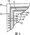
有鉴于此,美国专利第5,581,122、5,545,923及5,726,860号发明于基板上设置有接地环(Ground Ring)、电源环(Power Ring)及信号焊线垫(Signal Finger)的设计。如附图5及附图6所示的半导体结构中,于一基板10上表面100的芯片接置区101以外的区域布设有一接地环11、一电源环12及多条信号焊线垫13。接置一芯片14于该芯片接置区101后,遂进行打线(Wire Bonding)作业,以形成多条接地线(GroundWire)15、电源线(Power Wire)16及信号线(Signal Wire)17;接地线15是连接该芯片14上的该焊垫140至接地环11,电源线16连接该焊垫140至电源环12,信号线17则连接该焊垫140至信号焊线垫13。之后,在后续制造过程中,植接多个焊球18于基板10的下表面102上,并经由导电迹线19使焊球18与该接地环11、电源环12及信号焊线垫13电性连通,如此就能与外界装置(未图标)电性相通而使芯片14得以进行运作。须知,图标仅为说明之用,故皆为简化的结构,实际上的结构则精密复杂许多。In view of this, U.S. Patent No. 5,581,122, 5,545,923 and 5,726,860 invented the design of ground ring, power ring and signal pad (Signal Finger) on the substrate. In the semiconductor structure shown in FIG. 5 and FIG. 6 , a
然而上述半导体结构的设计却有诸多缺点。首先,接地环及电源环的设置占据基板面积造成基板上布局(Routability)的限制,不利于高密度输入/出连接端的设置及芯片高度集成化的发展,且基板尺寸无法进一步缩减,故不符合半导体结构轻薄短小的要求。再者,为减少信号的噪声,现有半导体结构通常还在基板上设计有去耦装置(Decoupling Pad)(未图标),以供安置电容器(Capacitor)(未图标)用以减少噪声,如此则更限制基板上的布局。此外,需形成众多接地线、电源线及信号线,进一步增加制造过程的复杂性,如附图6所示,该焊线以多层布设,故需精确控制不同层之间焊线线弧(Loop)的高度,无疑使制造过程的困难提高,且多层的焊线会造成模压(Molding)作业的困难,于模压注胶时,模流(Mold Flow)冲击力(Impact)极可能导致焊线间彼此触碰而发生短路(Short)现象,这会严重影响产品的优良率。However, the design of the above-mentioned semiconductor structure has many disadvantages. First of all, the setting of the grounding ring and the power ring occupies the area of the substrate, resulting in the limitation of the layout (Routability) on the substrate, which is not conducive to the setting of high-density input/output connection terminals and the development of highly integrated chips, and the size of the substrate cannot be further reduced, so it does not meet the requirements. Requirements for light, thin and short semiconductor structures. Furthermore, in order to reduce the noise of the signal, the existing semiconductor structure is usually also designed with a decoupling pad (Decoupling Pad) (not shown) on the substrate for placing a capacitor (Capacitor) (not shown) in order to reduce noise, so that The layout on the substrate is more restricted. In addition, many ground wires, power wires, and signal wires need to be formed, which further increases the complexity of the manufacturing process. As shown in Figure 6, the bonding wires are laid out in multiple layers, so it is necessary to accurately control the arcs of the bonding wires between different layers ( The height of the Loop will undoubtedly increase the difficulty of the manufacturing process, and the multi-layer welding wire will cause difficulties in the molding operation. When the mold is injected, the impact of the mold flow is likely to cause welding The short circuit (Short) phenomenon occurs when the wires touch each other, which will seriously affect the good rate of the product.
因此,如何有效解决上述缺陷,开发出一种高电性且不增加基板上布局限制并确保制成品优良率的半导体装置,实为一个需要探讨的课题。Therefore, how to effectively solve the above-mentioned defects, and develop a semiconductor device with high electrical performance without increasing layout restrictions on the substrate and ensuring the yield of finished products is actually a subject to be discussed.
发明内容Contents of the invention
本发明的一目的在于提供一种不需设置电源环及接地环的球栅阵列半导体封装件。An object of the present invention is to provide a ball grid array semiconductor package that does not require a power ring and a ground ring.
本发明的另一目的在于提供一种不需布设电源线及接地线的球栅阵列半导体封装件。Another object of the present invention is to provide a ball grid array semiconductor package that does not need to lay out power lines and ground lines.
本发明的再一目的在于提供一种不会增加基板上布局限制的球栅阵列半导体封装件。Yet another object of the present invention is to provide a ball grid array semiconductor package that does not increase layout constraints on a substrate.
本发明的又一目的在于提供一种得以增加散热效率并具屏蔽功能的球栅阵列半导体封装件。Another object of the present invention is to provide a ball grid array semiconductor package with improved heat dissipation efficiency and shielding function.
为达成上述及其它目的,发明了一种球栅阵列半导体封装件。该半导体封装件是包括:一基板,具有一第一表面与一相对的第二表面,于该基板的第一表面上界定有一芯片接置区,于该芯片接置区周围布设有多条信号焊线垫(Signal Finger),并于该信号焊线垫外的区域形成有一电源片接置区及一接地片接置区分别位于该基板的两侧;至少一芯片,具有一作用表面(Active Surface)与一相对的非作用表面(Non-active Surface),于该芯片作用表面上的周围位置处布设有多条信号焊垫(Signal Pad)、电源焊垫(Power Pad)及接地焊垫(Ground Pad),并于该作用表面上没有布设焊垫的区域形成有一电源层(Power Plane)及一接地层(Ground Plane),该电源焊垫是整合(Consolidate)并电性连通至该电源层,且该接地焊垫是整合并电性连通至该接地层,同时,该芯片的非作用表面是粘接于该基板的芯片接置区上,使该芯片上的电源层及接地层分别朝向该基板的电源片接置区及接地片接置区;多条焊线,用以电性连接该芯片的信号焊垫至该基板第一表面上的信号焊线垫;一电源片(Power Plate),其一端粘接于该芯片的电源层,另一端粘接至该基板的电源片接置区,且该电源片以不影响该焊线布设的方式设置;一接地片(Ground Plate),其一端粘接于该芯片的接地层,另一端粘接至该基板的接地片接置区,且该接地片以不影响该焊线布设的方式设置;一封装胶体,形成于该基板的第一表面上,用以包覆该芯片、该焊线、该电源片及该接地片;以及多个焊球,植接于该基板第二表面上。To achieve the above and other objectives, a ball grid array semiconductor package is invented. The semiconductor package includes: a substrate with a first surface and an opposite second surface, a chip connection area is defined on the first surface of the substrate, and a plurality of signal lines are arranged around the chip connection area. Welding wire pad (Signal Finger), and in the area outside the signal welding pad, a power supply piece connection area and a ground piece connection area are respectively located on both sides of the substrate; at least one chip has an active surface (Active Surface) and an opposite non-active surface (Non-active Surface), a plurality of signal pads (Signal Pad), power pads (Power Pad) and ground pads ( Ground Pad), and a power plane (Power Plane) and a ground plane (Ground Plane) are formed on the area where the pad is not arranged on the active surface, and the power pad is integrated (Consolidate) and electrically connected to the power plane , and the ground pad is integrated and electrically connected to the ground layer. At the same time, the non-active surface of the chip is bonded to the chip landing area of the substrate, so that the power layer and the ground layer on the chip face respectively The power plate connecting area and the grounding plate connecting area of the substrate; a plurality of bonding wires for electrically connecting the signal pads of the chip to the signal bonding pads on the first surface of the substrate; a power plate (Power Plate ), one end of which is bonded to the power layer of the chip, and the other end is bonded to the power chip connection area of the substrate, and the power chip is arranged in a manner that does not affect the wiring of the bonding wire; a ground plate (Ground Plate), One end of it is bonded to the ground layer of the chip, and the other end is bonded to the ground pad area of the substrate, and the ground pad is arranged in a manner that does not affect the wiring of the bonding wire; an encapsulant is formed on the first One surface is used to cover the chip, the welding wire, the power pad and the ground pad; and a plurality of solder balls are planted on the second surface of the substrate.
其中,该基板的第二表面上预定位置处形成有多条信号焊球垫(Signal Ball Pad)、电源焊球垫(Power Ball Pad)及接地焊球垫(GroundBall Pad),并该基板形成有多条贯穿该基板的通孔(Via),该通孔用以使该信号焊球垫与该基板第一表面上的信号焊线垫电性连通,且使该电源焊球垫及接地焊球垫分别与该基板第一表面上的电源片接置区及接地片接置区电性连通;而该焊球则植接于该基板第二表面的该信号焊球垫、电源焊球垫及接地焊球垫上。再者,该芯片作用表面上的电源焊垫及接地焊垫以重配(Re-distribution)方式形成有多条引线,该引线用以使该电源焊垫及接地焊垫分别电性连通至该电源层及接地层。Wherein, a plurality of signal ball pads (Signal Ball Pad), power ball pads (Power Ball Pad) and ground ball pads (GroundBall Pad) are formed at predetermined positions on the second surface of the substrate, and the substrate is formed with A plurality of through holes (Via) penetrating the substrate, the through holes are used to electrically communicate the signal solder ball pad with the signal solder wire pad on the first surface of the substrate, and to make the power solder ball pad and the ground solder ball The pads are respectively electrically connected with the power pads and the ground pads on the first surface of the substrate; and the solder balls are implanted on the signal pads, power pads and ground on the solder ball pad. Furthermore, the power pad and the ground pad on the active surface of the chip form a plurality of lead wires in a re-distribution manner, and the lead wires are used to electrically connect the power pad and the ground pad respectively to the power plane and ground plane.
以金属材质制成的电源片,形成有一突出部(Protruding Portion)、一平坦部(Flat Portion)及一支撑部(Supporting Portion),该突出部是以导电性黏胶如银胶粘接于该芯片的电源层,该支撑部亦以导电性黏胶粘接于该基板的电源片接置区,使该平坦部为该突出部及支撑部所支撑于该芯片上方而不影响该焊线的布设。同理,该接地片亦得以金属材质制成,并以导电性黏胶粘接于该芯片及基板上,其中,该接地片亦形成有一突出部、一平坦部及一支撑部,该突出部粘接于该芯片的接地层,该支撑部粘接于该基板的接地片接置区,使该平坦部为该突出部及支撑部所支撑于该芯片上方而不影响该焊线的布设。The power chip made of metal material is formed with a protruding portion (Protruding Portion), a flat portion (Flat Portion) and a supporting portion (Supporting Portion), and the protruding portion is bonded to the The power supply layer of the chip, the support part is also bonded to the power chip connection area of the substrate with conductive adhesive, so that the flat part is supported by the protruding part and the support part above the chip without affecting the bonding wire layout. Similarly, the ground sheet can also be made of metal material, and bonded on the chip and the substrate with conductive adhesive, wherein, the ground sheet also forms a protruding portion, a flat portion and a supporting portion, and the protruding portion The support portion is bonded to the ground layer of the chip, and the support portion is bonded to the ground sheet connection area of the substrate, so that the flat portion is supported by the protruding portion and the support portion above the chip without affecting the wiring of the bonding wire.
在上述的结构中,采用电源片及接地片的方式以取代现有封装件布设的电源线及接地线,具有诸多优点。首先,基板上无需设置用以分别连接电源线及接地线的电源环及接地环,因电源环及接地环占据基板而限制基板上布局(Routability)的缺点得以克服。再者,无需布设电源线及接地线,而仅形成有连接信号焊垫至信号焊线垫的焊线,故在模压时焊线间发生短路(Short)的机率得以降低,并使制造过程简化,提高产品的优良率。此外,电源片及接地片还可提供屏蔽(Shielding)功能,使芯片免受外界的电磁干扰(Electric Magnetic Interference,EMI),有助于提升半导体封装件的性能。In the above structure, using the power strip and the ground strip to replace the power line and the ground line arranged in the existing package has many advantages. Firstly, there is no need to arrange a power ring and a ground ring on the substrate for respectively connecting the power line and the ground line, and the disadvantage of limiting the layout (Routability) on the substrate due to the power ring and the ground ring occupying the substrate is overcome. Furthermore, there is no need to lay out power lines and ground lines, but only the bonding wires connecting the signal pads to the signal pads are formed, so the probability of short circuit (Short) between the bonding wires during molding is reduced, and the manufacturing process is simplified. , Improve the excellent rate of the product. In addition, the power strip and the ground strip can also provide a shielding function to protect the chip from external electromagnetic interference (Electric Magnetic Interference, EMI), which helps to improve the performance of the semiconductor package.
另一方面,该电源片平坦部的顶面得与该接地片平坦部的顶面呈共平面方式设置,使该电源片的顶面与该接地片的顶面外露出该封装胶体。此种设计则有助于借由外露的电源片及接地片表面排除芯片所产生的热能,故得以有效增进封装件的散热效率。On the other hand, the top surface of the flat portion of the power pad and the top surface of the flat portion of the ground pad are coplanar, so that the top surface of the power pad and the top surface of the ground pad expose the encapsulant. This design helps to dissipate the heat energy generated by the chip through the exposed surfaces of the power pad and the ground pad, thus effectively improving the heat dissipation efficiency of the package.
附图说明Description of drawings
为让本发明的上述和其它目的、特征以及优点能更明显易懂,将与较佳实施例,并配合附图,详细说明本发明的实施例,附图的内容简述如下:In order to make the above-mentioned and other objects, features and advantages of the present invention more obvious and understandable, the embodiments of the present invention will be described in detail in conjunction with the preferred embodiments and accompanying drawings. The contents of the accompanying drawings are briefly described as follows:
附图1是本发明半导体封装件的第一实施例的剖视图;Accompanying drawing 1 is the sectional view of the first embodiment of semiconductor package of the present invention;
附图2A是本发明半导体封装件的芯片的上视图;Accompanying drawing 2A is the top view of the chip of semiconductor package of the present invention;
附图2B是附图2A沿2B-2B线切开的局部剖视图;Accompanying drawing 2B is the partial sectional view of accompanying drawing 2A cut along 2B-2B line;
附图3A至附图3F是显示本发明半导体封装件的第一实施例的制造过程剖面示意图;3A to 3F are schematic cross-sectional views showing the manufacturing process of the first embodiment of the semiconductor package of the present invention;
附图4是本发明半导体封装件的第二实施例的剖视图;Accompanying drawing 4 is the sectional view of the second embodiment of the semiconductor package of the present invention;
附图5是一现有半导体结构的剖视图;以及Accompanying drawing 5 is a cross-sectional view of a conventional semiconductor structure; and
附图6是附图5半导体结构的局部上视图。Accompanying drawing 6 is a partial top view of the semiconductor structure of Fig. 5 .
符号说明Symbol Description
1 半导体结构 10 基板1
100 上表面 101 芯片接置区100 upper surface 101 chip landing area
102 下表面 11 接地环102
12 电源环 13 信号焊线垫12
14 芯片 140 焊垫14
15 接地线 16 电源线15
17 信号线 18 焊球17 Signal wire 18 Solder ball
19 导电迹线19 Conductive traces
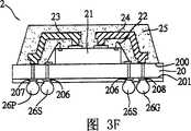
2 半导体封装件 20 基板2
200 第一表面 201 第二表面200
202 芯片接置区 203 信号焊线垫202
204 电源片接置区 205 接地片接置区204
206 信号焊球垫 207 电源焊球垫206
208 接地焊球垫 209 拒焊剂层208 Ground
21 芯片 210 作用表面21 chip 210 active surface
211 非作用表面 212 信号焊垫211 Non-active surface 212 Signal pad
213 电源焊垫 214 接地焊垫213 Power pad 214 Ground pad
215 电源层 216 接地层215 power plane 216 ground plane
217 引线 218 隔层217 Lead wire 218 Compartment
219 隔层 22 焊线219
23 电源片 230 突出部23 Power piece 230 Protrusion
231 平坦部 232 支撑部231 Flat part 232 Support part
24 接地片 240 突出部24 Ground piece 240 Protrusion
241 平坦部 242 支撑部241 Flat part 242 Support part
25 封装胶体 26S 信号焊球25
26P 电源焊球 26G 接地焊球26P
27 通孔 28 导电性黏胶27 Through-hole 28 Conductive adhesive
3 半导体封装件 30 电源片3
300 平坦部 301 顶面300
31 接地片 310 平坦部31
311 顶面 32 封装胶体 33 芯片311
具体实施方式Detailed ways
实施例1Example 1
如附图1所示为本发明的球栅阵列半导体封装件2;附图2A所示为本发明半导体封装件2所使用的芯片21。如图所示,该半导体封装件2是包括:一基板20,具有一第一表面200与一相对的第二表面201,于该基板20的第一表面200上界定有一芯片接置区202,于该芯片接置区202周围布设有多条信号焊线垫(Signal Finger)203,并于该信号焊线垫203外的区域形成有一电源片接置区204及一接地片接置区205分别位于该基板20的两侧;至少一芯片21,具有一作用表面(ActiveSurface)210与一相对的非作用表面(Non-active Surface)211,于该芯片21作用表面210上的周围位置处,布设有多条信号焊垫(Signal Pad)212、电源焊垫(Power Pad)213及接地焊垫(Ground Pad)214,并于该作用表面210上没有布设焊垫的区域形成有一电源层(Power Plane)215及一接地层(Ground Plane)216,该电源焊垫213是整合(Consolidate)并电性连通至该电源层215,且该接地焊垫214是整合并电性连通至该接地层216,同时,该芯片21的非作用表面211是粘接于该基板20的芯片接置区202上,使该芯片21上的电源层215及接地层216分别朝向该基板20的电源片接置区204及接地片接置区205;多条焊线22,用以电性连接该芯片21的信号焊垫212至该基板20第一表面200上的信号焊线垫203;一电源片(Power Plate)23,其一端粘接于该芯片21的电源层215,另一端粘接至该基板20的电源片接置区204,且该电源片23以不影响该焊线22布设的方式设置;一接地片(Ground Plate)24,其一端粘接于该芯片21的接地层216,另一端粘接至该基板20的接地片接置区205,且该接地片24以不影响该焊线22布设的方式设置;一封装胶体25,形成于该基板20的第一表面200上,用以包覆该芯片21、该焊线22、该电源片23及该接地片24;以及多条信号焊球26S、电源焊球26P及接地焊球26G,植接于该基板20的第二表面201上。FIG. 1 shows the ball grid array semiconductor package 2 of the present invention; FIG. 2A shows the
上述球栅阵列半导体封装件2是如附图3A至附图3F所示的步骤而制得。首先,如附图3A所示,制备一具有一作用表面210与一相对的非作用表面211的芯片21。如附图2A所示,于该芯片21作用表面210上的周围位置处布设有多条信号焊垫212、电源焊垫213及接地焊垫214。由于此焊垫的制法均采用现有技术,故于此不予以赘述。须知,图标焊垫的数目仅为简化说明而设,焊垫数目应视实际需要而设置。The above ball grid array semiconductor package 2 is manufactured through the steps shown in FIG. 3A to FIG. 3F . First, as shown in FIG. 3A , a
如附图3B及附图2A所示,于该芯片21作用表面210上的电源焊垫213以重配(Re-distribution)方式形成有多条引线217,用以使该电源焊垫213经由该引线217整合并电性连通至一电源层215,同时,该接地焊垫214亦以重配方式形成的引线217而整合并电性连通至一接地层216。此述的重配技术,如附图2B所示,于外露出隔层(PassivatingFilm)218的电源焊垫213上以导电性材质如铝(Aluminum)或铜(Copper)形成引线217,还在引线217上涂布一绝缘性物质如氧化硅(SiliconOxide)或氮化硅(Silicon Nitride)以形成另一隔层219,并去除部分隔层219,以外露出部分引线217,所有电源焊垫213的引线217外露部分则整合形成电源层215。同理,接地层216亦以如附图2B所示的方式形成,故于此不予以赘述。As shown in FIG. 3B and FIG. 2A , a plurality of leads 217 are formed on the power pad 213 on the active surface 210 of the
如附图3C所示,制备一具有一第一表面200与一相对的第二表面201的基板20,于该基板20的第一表面200上界定有一芯片接置区202,于该芯片接置区202周围布设有多条信号焊线垫203,并于该信号焊线垫203外的区域形成有一电源片接置区204及一接地片接置区205分别位于该基板20的两侧。该基板20的第二表面201上预定位置处形成有多条信号焊球垫(Signal Ball Pad)206、电源焊球垫(Power BallPad)207及接地焊球垫(Ground Ball Pad)208,其中,该基板20的第二表面201上还涂布有一拒焊剂(Solder Mask)层209,用以保护该基板20的第二表面201,并使该焊球垫外露出该拒焊剂层209以供后续植球之用。又,该基板20形成有多个贯穿该基板的通孔(Via)27,该通孔27作用是使该信号焊球垫206与该基板20第一表面200上的信号焊线垫203电性连通,且使该电源焊球垫207及接地焊球垫208分别与该基板20第一表面200上的电源片接置区204及接地片接置区205电性连通。As shown in FIG. 3C , prepare a
如附图3D所示,粘接该芯片21的非作用表面211至该基板20的芯片接置区202上,使该芯片21上的电源层215及接地层216分别朝向该基板20的电源片接置区204及接地片接置区205。再进行焊线(Wire Bonding)作业,用以形成多条焊线22,如金线,使该芯片21的信号焊垫212电性连接至该基板20第一表面200上的信号焊线垫203。As shown in FIG. 3D, the non-active surface 211 of the
如附图3E所示,以导电性黏胶28如银胶粘接一金属材质制成的电源片23的两端分别于该芯片21及基板20上。该电源片23形成有一突出部(Protruding Portion)230、一平坦部(Flat Portion)231及一支撑部(Supporting Portion)232,该突出部230是粘接于该芯片21的电源层215,而该支撑部232粘接于该基板20的电源片接置区204,使该平坦部231为该突出部230及支撑部232所支撑于该芯片21上方而不影响该焊线22的布设。同时,一金属材质制成的接地片24亦使用该导电性黏胶28粘接其两端分别于该芯片21及基板20上,其中,该接地片24亦形成有一突出部240、一平坦部241及一支撑部242,该突出部240粘接于该芯片21的接地层216,该支撑部242粘接于该基板20的接地片接置区205,使该平坦部241为该突出部240及支撑部242所支撑于该芯片21上方而不影响该焊线22的布设。然而,此电源片23及接地片24呈现的形状,并不受限于此实施例所述的形状,须知,任何其它可达到相同功能的形状,皆为本发明的范畴所涵盖。As shown in FIG. 3E , the two ends of a
如附图3F所示,进行模压(Molding)作业,使用一树脂化合物如环氧树脂(Epoxy Resin)于该基板20的第一表面200上形成一封装胶体25,以使该芯片21、该焊线22、该电源片23及该接地片24为该封装胶体25所包覆,从而免受外界水气或污染物质所侵害。然后,进行植球(Ball Implantation)作业,分别植接多条信号焊球26S、电源焊球26P及接地焊球26G于该基板20第二表面201的该信号焊球垫206、电源焊球垫207及接地焊球垫208上,此类焊球26的作用是使该芯片21得以与外界装置(未图标)电性连接。如此则完成本发明的半导体封装件2。由于模压与植球过程均为现有技术,故于此不予以赘述。As shown in accompanying drawing 3F, carry out mold pressing (Molding) operation, use a resin compound such as epoxy resin (Epoxy Resin) to form an
与现有半导体封装件相比较,本发明的特征在于采用电源片及接地片以取代现有封装件布设的电源线及接地线,其优点如下:首先,基板上无需设置用以分别连接电源线及接地线的电源环及接地环,因此电源环及接地环占据基板而限制基板上布局(Routability)的缺点得以屏除。再者,比较于现有技术所布设的电源线及接地线,电源片及接地片的设置在整个制造过程中较为简化,且本发明封装件中仅形成有连接信号焊垫至信号焊线垫的焊线,故在模压时焊线间发生短路(Short)的机率得以降低,使产品的优良率提高。此外,电源片及接地片还可提供屏蔽(Shielding)功能,使芯片免于受外界的电磁干扰(ElectricMagnetic Interference,EMI),有助于提升半导体封装件的性能。Compared with the existing semiconductor packages, the present invention is characterized in that the power strips and the ground strips are used to replace the power lines and ground lines arranged in the existing packages. And the power ring and the ground ring of the ground wire, so the disadvantage that the power ring and the ground ring occupy the substrate and limit the layout (Routability) on the substrate can be eliminated. Furthermore, compared with the power line and ground line laid out in the prior art, the arrangement of the power supply plate and the ground plate is relatively simplified in the whole manufacturing process, and only the connection signal pads to the signal pads are formed in the package of the present invention. Therefore, the probability of short circuit (Short) between welding wires during molding is reduced, which improves the yield of products. In addition, the power strip and the ground strip can also provide a shielding function to protect the chip from external electromagnetic interference (Electric Magnetic Interference, EMI), which helps to improve the performance of the semiconductor package.
实施例2Example 2
附图4所示为本发明半导体封装件的第二实施例。如图所示,本发明第二实施例的半导体封装件3是大致上与第一实施例的半导体封装件2相同,不同之处仅在于电源片30平坦部300的顶面301得与接地片31的平坦部310的顶面311呈共平面方式设置。在进行模压作业时,封装模具(未图标)的顶壁得直接压置于该电源片30的顶面301及接地片31的顶面311上,使该顶面301,311不为封装胶体32所包覆,故在封装胶体32形成后,该电源片30的顶面301及接地片31的顶面311得以外露出该封装胶体32。由于该电源片30及接地片31是以金属材质制成,此种顶面外露的设计,有助于使芯片33所产生的热量经由该电源片30及接地片31,以及其外露的顶面301,311而散逸至封装件3外,故有效增进该封装件3的散热效率。FIG. 4 shows a second embodiment of the semiconductor package of the present invention. As shown in the figure, the semiconductor package 3 of the second embodiment of the present invention is substantially the same as the semiconductor package 2 of the first embodiment, the only difference is that the
以上所述,仅是用以说明本发明的具体实施例而已,并非用以限定本发明的可实施范围,在未脱离本发明权利要求书中所限定的精神与原理下完成的一切等效改变或修饰,皆属于本专利的保护范围之内。The above description is only used to illustrate the specific embodiments of the present invention, and is not used to limit the scope of the present invention. All equivalent changes can be made without departing from the spirit and principle defined in the claims of the present invention. Or modification, all belong to the scope of protection of this patent.
Claims (20)
Priority Applications (1)
| Application Number | Priority Date | Filing Date | Title |
|---|---|---|---|
| CNB021231923ACN1303685C (en) | 2002-06-28 | 2002-06-28 | Ball Grid Array Semiconductor Package |
Applications Claiming Priority (1)
| Application Number | Priority Date | Filing Date | Title |
|---|---|---|---|
| CNB021231923ACN1303685C (en) | 2002-06-28 | 2002-06-28 | Ball Grid Array Semiconductor Package |
Publications (2)
| Publication Number | Publication Date |
|---|---|
| CN1466206A CN1466206A (en) | 2004-01-07 |
| CN1303685Ctrue CN1303685C (en) | 2007-03-07 |
Family
ID=34142307
Family Applications (1)
| Application Number | Title | Priority Date | Filing Date |
|---|---|---|---|
| CNB021231923AExpired - Fee RelatedCN1303685C (en) | 2002-06-28 | 2002-06-28 | Ball Grid Array Semiconductor Package |
Country Status (1)
| Country | Link |
|---|---|
| CN (1) | CN1303685C (en) |
Families Citing this family (7)
| Publication number | Priority date | Publication date | Assignee | Title |
|---|---|---|---|---|
| CN100373596C (en)* | 2004-09-07 | 2008-03-05 | 日月光半导体制造股份有限公司 | Ball grid array package substrate, manufacturing method thereof and ball grid array package structure thereof |
| CN100495699C (en)* | 2007-06-14 | 2009-06-03 | 日月光半导体制造股份有限公司 | Semiconductor packaging structure with electromagnetic shielding function and manufacturing method thereof |
| CN101378023B (en)* | 2007-08-27 | 2010-12-01 | 矽品精密工业股份有限公司 | Semiconductor package and fabrication method thereof |
| US7800208B2 (en)* | 2007-10-26 | 2010-09-21 | Infineon Technologies Ag | Device with a plurality of semiconductor chips |
| JP2013222829A (en)* | 2012-04-17 | 2013-10-28 | Taiyo Yuden Co Ltd | Circuit module and manufacturing method thereof |
| CN103400826B (en)* | 2013-06-21 | 2016-08-17 | 三星半导体(中国)研究开发有限公司 | Semiconductor packages and manufacture method thereof |
| CN103400816B (en)* | 2013-06-26 | 2016-08-10 | 三星半导体(中国)研究开发有限公司 | Packaging part and manufacture method thereof |
Citations (3)
| Publication number | Priority date | Publication date | Assignee | Title |
|---|---|---|---|---|
| JPH09148478A (en)* | 1995-11-21 | 1997-06-06 | Hitachi Ltd | Semiconductor integrated circuit device |
| US6034423A (en)* | 1998-04-02 | 2000-03-07 | National Semiconductor Corporation | Lead frame design for increased chip pinout |
| US6201298B1 (en)* | 1998-04-28 | 2001-03-13 | Nec Corporation | Semiconductor device using wiring tape |
- 2002
- 2002-06-28CNCNB021231923Apatent/CN1303685C/ennot_activeExpired - Fee Related
Patent Citations (3)
| Publication number | Priority date | Publication date | Assignee | Title |
|---|---|---|---|---|
| JPH09148478A (en)* | 1995-11-21 | 1997-06-06 | Hitachi Ltd | Semiconductor integrated circuit device |
| US6034423A (en)* | 1998-04-02 | 2000-03-07 | National Semiconductor Corporation | Lead frame design for increased chip pinout |
| US6201298B1 (en)* | 1998-04-28 | 2001-03-13 | Nec Corporation | Semiconductor device using wiring tape |
Also Published As
| Publication number | Publication date |
|---|---|
| CN1466206A (en) | 2004-01-07 |
Similar Documents
| Publication | Publication Date | Title |
|---|---|---|
| US6667546B2 (en) | Ball grid array semiconductor package and substrate without power ring or ground ring | |
| US10854575B2 (en) | Three-dimensional (3D) package structure having an epoxy molding compound layer between a discrete inductor and an encapsulating connecting structure | |
| US6534859B1 (en) | Semiconductor package having heat sink attached to pre-molded cavities and method for creating the package | |
| KR101521255B1 (en) | Integrated circuit package system with dual connections | |
| US6720649B2 (en) | Semiconductor package with heat dissipating structure | |
| US7884486B2 (en) | Chip-stacked package structure and method for manufacturing the same | |
| KR20140057979A (en) | Semiconductor package and method of manufacturing the semiconductor package | |
| CN1685509A (en) | Electronic package with backside cavity-mounted capacitor and method of processing the same | |
| KR20140057982A (en) | Semiconductor package and method of manufacturing the semiconductor package | |
| JP2020088366A (en) | Semiconductor package with in-package compartmental shielding and fabrication method thereof | |
| US20200168557A1 (en) | Semiconductor package and fabrication method thereof | |
| CN1574308A (en) | Thermally enhanced component substrate | |
| CN1971894A (en) | Chip-embedded modular structure | |
| JP6802314B2 (en) | Semiconductor package and its manufacturing method | |
| CN1303685C (en) | Ball Grid Array Semiconductor Package | |
| CN1716581A (en) | Device mounting board | |
| CN1521816A (en) | Semiconductor chip packaging structure and manufacturing method thereof | |
| CN1210789C (en) | Semiconductor package element with heat dissipation structure | |
| CN1767178A (en) | Semiconductor carrier board, manufacturing method thereof, and semiconductor package assembly | |
| CN1914727A (en) | Electronic component and method for manufacturing the same | |
| CN216671634U (en) | Multi-chip packaging piece | |
| CN1216423C (en) | Semiconductor device and its manufacturing method | |
| CN1750259A (en) | Lead frame for multi-chip package, manufacturing method and package structure thereof | |
| CN2653693Y (en) | Chip packaging structure | |
| CN114334938B (en) | Multi-chip package and manufacturing method thereof |
Legal Events
| Date | Code | Title | Description |
|---|---|---|---|
| C10 | Entry into substantive examination | ||
| SE01 | Entry into force of request for substantive examination | ||
| C06 | Publication | ||
| PB01 | Publication | ||
| C10 | Entry into substantive examination | ||
| SE01 | Entry into force of request for substantive examination | ||
| C14 | Grant of patent or utility model | ||
| GR01 | Patent grant | ||
| CF01 | Termination of patent right due to non-payment of annual fee | ||
| CF01 | Termination of patent right due to non-payment of annual fee | Granted publication date:20070307 Termination date:20210628 |