CN1301178C - Patterning of Microstructures in Semiconductors by Ultraviolet Laser Ablation - Google Patents
Patterning of Microstructures in Semiconductors by Ultraviolet Laser AblationDownload PDFInfo
- Publication number
- CN1301178C CN1301178CCNB028044045ACN02804404ACN1301178CCN 1301178 CCN1301178 CCN 1301178CCN B028044045 ACNB028044045 ACN B028044045ACN 02804404 ACN02804404 ACN 02804404ACN 1301178 CCN1301178 CCN 1301178C
- Authority
- CN
- China
- Prior art keywords
- laser system
- laser
- output
- substrate material
- microns
- Prior art date
- Legal status (The legal status is an assumption and is not a legal conclusion. Google has not performed a legal analysis and makes no representation as to the accuracy of the status listed.)
- Expired - Fee Related
Links
Images


Classifications
- B—PERFORMING OPERATIONS; TRANSPORTING
- B23—MACHINE TOOLS; METAL-WORKING NOT OTHERWISE PROVIDED FOR
- B23K—SOLDERING OR UNSOLDERING; WELDING; CLADDING OR PLATING BY SOLDERING OR WELDING; CUTTING BY APPLYING HEAT LOCALLY, e.g. FLAME CUTTING; WORKING BY LASER BEAM
- B23K26/00—Working by laser beam, e.g. welding, cutting or boring
- B23K26/02—Positioning or observing the workpiece, e.g. with respect to the point of impact; Aligning, aiming or focusing the laser beam
- B23K26/06—Shaping the laser beam, e.g. by masks or multi-focusing
- B23K26/062—Shaping the laser beam, e.g. by masks or multi-focusing by direct control of the laser beam
- B23K26/0626—Energy control of the laser beam
- B—PERFORMING OPERATIONS; TRANSPORTING
- B23—MACHINE TOOLS; METAL-WORKING NOT OTHERWISE PROVIDED FOR
- B23K—SOLDERING OR UNSOLDERING; WELDING; CLADDING OR PLATING BY SOLDERING OR WELDING; CUTTING BY APPLYING HEAT LOCALLY, e.g. FLAME CUTTING; WORKING BY LASER BEAM
- B23K26/00—Working by laser beam, e.g. welding, cutting or boring
- B23K26/08—Devices involving relative movement between laser beam and workpiece
- B23K26/083—Devices involving movement of the workpiece in at least one axial direction
- B23K26/0853—Devices involving movement of the workpiece in at least in two axial directions, e.g. in a plane
- B—PERFORMING OPERATIONS; TRANSPORTING
- B23—MACHINE TOOLS; METAL-WORKING NOT OTHERWISE PROVIDED FOR
- B23K—SOLDERING OR UNSOLDERING; WELDING; CLADDING OR PLATING BY SOLDERING OR WELDING; CUTTING BY APPLYING HEAT LOCALLY, e.g. FLAME CUTTING; WORKING BY LASER BEAM
- B23K26/00—Working by laser beam, e.g. welding, cutting or boring
- B23K26/08—Devices involving relative movement between laser beam and workpiece
- B23K26/0869—Devices involving movement of the laser head in at least one axial direction
- B23K26/0876—Devices involving movement of the laser head in at least one axial direction in at least two axial directions
- B23K26/0884—Devices involving movement of the laser head in at least one axial direction in at least two axial directions in at least in three axial directions, e.g. manipulators, robots
- B—PERFORMING OPERATIONS; TRANSPORTING
- B23—MACHINE TOOLS; METAL-WORKING NOT OTHERWISE PROVIDED FOR
- B23K—SOLDERING OR UNSOLDERING; WELDING; CLADDING OR PLATING BY SOLDERING OR WELDING; CUTTING BY APPLYING HEAT LOCALLY, e.g. FLAME CUTTING; WORKING BY LASER BEAM
- B23K26/00—Working by laser beam, e.g. welding, cutting or boring
- B23K26/36—Removing material
- B23K26/40—Removing material taking account of the properties of the material involved
- B—PERFORMING OPERATIONS; TRANSPORTING
- B23—MACHINE TOOLS; METAL-WORKING NOT OTHERWISE PROVIDED FOR
- B23K—SOLDERING OR UNSOLDERING; WELDING; CLADDING OR PLATING BY SOLDERING OR WELDING; CUTTING BY APPLYING HEAT LOCALLY, e.g. FLAME CUTTING; WORKING BY LASER BEAM
- B23K2101/00—Articles made by soldering, welding or cutting
- B23K2101/36—Electric or electronic devices
- B23K2101/40—Semiconductor devices
- B—PERFORMING OPERATIONS; TRANSPORTING
- B23—MACHINE TOOLS; METAL-WORKING NOT OTHERWISE PROVIDED FOR
- B23K—SOLDERING OR UNSOLDERING; WELDING; CLADDING OR PLATING BY SOLDERING OR WELDING; CUTTING BY APPLYING HEAT LOCALLY, e.g. FLAME CUTTING; WORKING BY LASER BEAM
- B23K2103/00—Materials to be soldered, welded or cut
- B23K2103/50—Inorganic material, e.g. metals, not provided for in B23K2103/02 – B23K2103/26
- B23K2103/52—Ceramics
Landscapes
- Physics & Mathematics (AREA)
- Optics & Photonics (AREA)
- Engineering & Computer Science (AREA)
- Plasma & Fusion (AREA)
- Mechanical Engineering (AREA)
- Robotics (AREA)
- Laser Beam Processing (AREA)
- Drying Of Semiconductors (AREA)
Abstract
Description
Translated fromChinese相关申请案Related applications
本专利申请案根据以下两申请案而主张优先权:2001年1月31日申请的第60/265,556号的美国临时申请案以及2001年3月9日申请的第09/803,382号美国专利申请案。This patent application claims priority from U.S. Provisional Application No. 60/265,556, filed January 31, 2001, and U.S. Patent Application No. 09/803,382, filed March 9, 2001 .
技术领域technical field
本发明是有关于以半导体烧蚀高速形成微尺度特征尺寸的方法以及/或是设备,特别是对于硅,其是使用紫外激光的脉冲输出。The present invention relates to methods and/or apparatus for high-speed formation of microscale features by ablation of semiconductors, particularly silicon, using the pulsed output of an ultraviolet laser.
背景技术Background technique
半导体工业使用多种技术来分割不同的电子元件,这些元件经常被称为晶粒(die),其是在制造该元件时从半导体晶片中分割。一种用来进行这种分割的普通方法是使用钻石切割机。用来降低半导体晶片中分配为切割道的面积的方法被要求能够在产生有用的晶粒时获得更大面积的晶片使用率,进而增加每一晶片的晶粒产出。激光技术提供一个这种降低半导体晶片切割的切割道尺寸的机会。The semiconductor industry uses a variety of techniques to separate the various electronic components, often referred to as die, from a semiconductor wafer during manufacture of the components. A common method used to perform this division is to use a diamond cutter. Methods for reducing the area of a semiconductor wafer allocated as dicing streets are required to achieve greater wafer area utilization while producing useful die, thereby increasing die yield per wafer. Laser technology offers one such opportunity to reduce the size of the scribe lines for dicing semiconductor wafers.
对那些熟悉本项技术的人来说,使用红外线激光,例如Q-开关式1064纳米Nd:YAG激光来进行硅激光过程是公知的。然而,由于硅在1064纳米是一个弱吸收体,操作在这个种波长或者接近这个波长时,激光切割过程遭遇到显著的问题。沿着晶片表面以及沿着切割壁上,割品质通常可以观察到具有硅再沉积所造成的污损。The use of infrared lasers, such as Q-switched 1064 nm Nd:YAG lasers, for silicon laser processes is well known to those familiar with the art. However, since silicon is a weak absorber at 1064 nm, the laser cutting process suffers from significant problems when operating at or near this wavelength. Along the wafer surface as well as along the cut walls, cut quality can often be observed with fouling caused by silicon redeposition.
Carlson等人在第4,541,035号的美国专利,以及Anthony在第4,589,190号的美国专利中描述使用1064纳米的脉冲输出所进行的硅元件特征尺寸制造,例如从一种整合到ESI模型:5激光标记系统的声光式Q-开关式红外线(1R)Nd:YAG激光。(也可参考T.R.Anthony在1982年十二月的应用物理杂志,53卷,第9154。9164页的“以激光钻孔及扩散所制这的二极管”)。Alcorn等人在第4,618,380号美国专利中也说明一种以激光处理硅元件来制这成像光谱仪的方法。US Patent No. 4,541,035 to Carlson et al., and US Patent No. 4,589,190 to Anthony describe silicon device feature size fabrication using a pulsed output of 1064 nm, for example from an integrated ESI model:5 laser marking system Acousto-optic Q-switched infrared (1R) Nd:YAG laser. (See also "Diodes Made by Laser Drilling and Diffusion" by T.R. Anthony, Journal of Applied Physics, Vol. 53, No. 9154, pp. 9164, December 1982). Alcorn et al. in US Patent No. 4,618,380 also describe a method of laser processing silicon components to make such an imaging spectrometer.
Wills等人在第5,543,365号的美国专利中,说明一个使用1064纳米的脉冲输出来在硅晶片中形成多晶硅条痕的激光标记设备,例如以具有超过4纳秒脉冲宽度的Nd:YAG激光的脉冲输出c替代地,他们提到532纳米的倍频波长可以被使用。Wills et al. in U.S. Patent No. 5,543,365 describe a laser marking apparatus for forming polysilicon streaks in a silicon wafer using a pulsed output of 1064 nanometers, for example with a Nd:YAG laser having a pulse width exceeding 4 nanoseconds Output c Alternatively, they mention that a doubled wavelength of 532 nm could be used.
在“以准分子对照Nd:YAG激光产生用在3D互连线路的硅通孔”(1992年IEEE/CHMT国际电子制造技术研讨会)这篇文章中,Lee等人报导了使用1064纳米以及532纳米波长的Nd:YAG激光来产生一个穿透硅晶片表面的通孔,以达成多晶片模块的生产目的。Lee报导了在以1064纳米激光在硅晶片中钻凿通孔时,一旦达到一个认可的深度时,熔融材料便频繁地在孔洞上的壁上凝聚。这个种明显的硅再沉积使得这些孔洞不合适进行进一步的处理。Lee报导了使用1064纳米的双钻孔过程来改善孔洞的品质。Lee说明了在穿孔过程中从灯泵浦Q-开关式Nd:YAG激光所输出的532纳米倍频脉冲激光的应用,该穿孔过程是使用对于入射激光光束偏置的旋转透镜,以切割在硅中的一个4密耳(大约100微米)直径的孔洞。他报导了在3千赫兹的脉冲重复频率,具有70纳秒的脉冲宽度时,每一脉冲833微焦的处理参数。沿着激光钻孔通孔的壁上以及周围的硅再沉积仍然被观察到,而且一种化学蚀刻过程被使用来清洁该孔洞。In the article "Generation of Through-Silicon Vias for 3D Interconnects Using Excimer-Controlled Nd:YAG Lasers" (1992 IEEE/CHMT International Symposium on Electronics Manufacturing Technology), Lee et al. reported the use of 1064 nm and 532 A Nd:YAG laser with a nanometer wavelength is used to create a through hole penetrating the surface of a silicon wafer for the purpose of producing multi-chip modules. Lee reported that when drilling vias in silicon wafers with a 1064nm laser, molten material frequently condensed on the walls of the holes once an acceptable depth was reached. This apparent redeposition of silicon makes the voids unsuitable for further processing. Lee reported using a 1064nm dual-drilling process to improve the quality of the holes. Lee demonstrates the use of frequency-doubled 532 nm pulsed laser output from a lamp-pumped Q-switched Nd:YAG laser in a perforation process using a rotating lens biased against the incident laser beam to cut in silicon A 4 mil (approximately 100 micron) diameter hole in the He reported processing parameters of 833 microjoules per pulse at a pulse repetition rate of 3 kHz with a pulse width of 70 ns. Silicon redeposition along and around the walls of the laser drilled vias was still observed, and a chemical etching process was used to clean the holes.
Lee进一步报导了使用在248纳米波长的一种准分子激光来在硅中钻孔的方法。他报导了使用极高的脉冲能量时得到的极平滑的侧边的孔洞。他报导了在250赫兹脉冲重复频率以及5密耳(大约125微米)大小聚焦光点时使用每一脉冲290毫焦的能量来在30秒中钻出穿透硅晶片的孔洞。他比较了使用他的532纳米Nd:YAG穿孔技术所需的3秒钻孔时间。Lee建议一个经由投射技术,以248纳米准分子激光来减少硅孔洞钻孔所需时间的方法。如那些熟悉习知本项技术的人将认知到的,对于需使用这种技术来形成的孔洞的每一个图案,这种技术依赖于一种适当的光圈遮罩。Lee further reported the use of an excimer laser at a wavelength of 248 nm to drill holes in silicon. He reported extremely smooth sided holes when using extremely high pulse energies. He reported using 290 millijoules of energy per pulse to drill holes through a silicon wafer in 30 seconds at a pulse repetition rate of 250 Hz and a focused spot size of 5 mils (about 125 microns). He compared the 3-second drilling time required using his 532nm Nd:YAG drilling technology. Lee suggested a method to reduce the time required to drill silicon vias with a 248nm excimer laser via projection technology. As those familiar with the art will appreciate, this technique relies on an appropriate aperture mask for each pattern of holes that is required to be formed using this technique.
在美国专利第5,870,421号中,Dahm讨论使用近红外线激光来进行硅晶片切割的问题。他提到当使用近红外线激光时,再沉积产生不良切割品质的主因是来自于使用宽度超过大约1纳秒的激光脉冲所产生。Dahm提到使用具有少于大约1纳秒的短脉冲宽度的近红外线激光来解决硅中近红外线波长的很深的吸收深度,其叙述在这种短的脉冲宽度时可以产生做为高度吸收层的表面电浆。Dahm也提到近红外线激光,例如1064纳米Nd:YAG激光,被用在高速度应用之中,因为的它们具有产生比紫外激光更大功率的能力,他讨论紫外激光无法生成足够的功率来进行高速的硅处理。In US Patent No. 5,870,421, Dahm discusses the use of near-infrared lasers for dicing silicon wafers. He mentioned that the main cause of poor cut quality from redeposition when using near-infrared lasers comes from using laser pulses wider than about 1 nanosecond. Dahm mentions the use of near-infrared lasers with short pulse widths of less than about 1 nanosecond to address the deep absorption depth of near-infrared wavelengths in silicon, stating that at such short pulse widths can be produced as highly absorbing layers. surface plasma. Dahm also mentioned that near-infrared lasers, such as 1064 nm Nd:YAG lasers, are used in high-speed applications because of their ability to generate more power than ultraviolet lasers, which he argues cannot generate enough power to perform High-speed silicon processing.
Owen等人在美国专利第5,593,606号中,说明了紫外激光系统的使用优点,其是于具有优点的参数中产生的激光输出脉冲来形成穿透多层元件中的至少两层的通孔。这些参数通常包含:具有时序性脉冲短于100纳秒宽度的非准分子输出脉冲、具有光点直径小于100微米的光点区域、以及在重复频率大于200赫兹时,在整个光点区域中大于100毫瓦的平均强度或是幅照。Owen et al., in US Patent No. 5,593,606, describe the advantage of using an ultraviolet laser system that produces laser output pulses within advantageous parameters to form vias through at least two layers in a multilayer component. These parameters typically include: non-excimer output pulses with sequential pulses shorter than 100 nanoseconds in width, spot regions with spot diameters smaller than 100 microns, and greater than Average intensity or radiation of 100 milliwatts.
在美国专利第5,841,099号中,Owen等人在与上面说明的相似参数中改变紫外激光的输出,以便当进行加工不同的材料时得到不同的功率密度。他它们以改变激光脉波重复频率来改变强度,以便政变冲击到工件的激光光点的能量密度以及/或是改变光点的大小。In US Patent No. 5,841,099, Owen et al. varied the output of an ultraviolet laser in similar parameters to those described above to obtain different power densities when processing different materials. They vary the intensity by varying the laser pulse repetition rate in order to coup the energy density of the laser spot impinging on the workpiece and/or to change the spot size.
在美国专利第5,751,585号中,Cutler等人说明一种高速,高精确度多重平台定位系统,用来进行多种工具的精确及快速的定位,例如与工件上面的靶材有关的激光光束。他们使用一多重速率定位器系统,该多重速率定位器系统是处理工件靶材定位指令以及将它们转换成对慢速及快速定位器的指令。这些定位器是依一串的定位资料的响应而移动,其并不一定要停止。在一个实施例中,这个种技术可以使整个大型工件的微小特征尺寸图案的激光微型加工可以进行,藉此允许激光微型加工部件的产能增加。In US Patent No. 5,751,585, Cutler et al. describe a high-speed, high-accuracy multi-stage positioning system for precise and rapid positioning of various tools, such as laser beams, relative to targets on workpieces. They use a multi-rate positioner system that processes workpiece target positioning commands and translates them into commands for slow and fast positioners. These locators move in response to a sequence of positioning data, and do not necessarily stop. In one embodiment, this technique enables laser micromachining of small feature size patterns throughout large workpieces, thereby allowing increased throughput of laser micromachined components.
发明内容Contents of the invention
本发明的目的是提供一种使用激光来产生半导体中微特征的改良方法,这些半导体包括硅、砷化嫁(GaAs)、碳化硅(SiC硅)、氮化硅(SiN),以及/或是锗:硅,以及/或是包含在半导体过程中被序列地处理的各种半导体,这些过程包含但是不限于光刻以及蚀刻,对于那些熟悉本项技术的人来说也包含那些为了在半导体基片上,包括半导体晶片上产生有用电子及光电子电路的附加层。It is an object of the present invention to provide an improved method of using laser light to produce microfeatures in semiconductors including silicon, silicon arsenide (GaAs), silicon carbide (SiC silicon), silicon nitride (SiN), and/or Germanium: Silicon, and/or various semiconductors that are sequentially processed in semiconductor processes including, but not limited to, photolithography and etching, including, for those skilled in the art, On-chip, including additional layers on a semiconductor wafer that generate useful electronic and optoelectronic circuits.
本发明的另一个目的是提供一种使用高可信度非准分子紫外激光的方法,该高可信度非准分子紫外激光可在高脉冲重复频率以高脉冲能量输出来运行。Another object of the present invention is to provide a method using a high reliability non-excimer ultraviolet laser that can be operated at high pulse energy output at a high pulse repetition rate.
本发明提供一种在使用紫外激光烧蚀的半导体工件中,快速及直接地形成具有小于50微米特征尺寸的图案。一个复合光束定位器用来在工件处将非准分子紫外激光的聚焦输出快速定位,该紫外激光可以高脉冲重复频率的每脉冲输出发射高能量。这些图案可以包含:形成例如用在集成电路连接的极高宽高比的圆柱形开口,如通孔或者是盲孔(blind vias);包含于硅晶片上的处理的晶粒的曲线或直线分割(singulation);微型程字切割以将在半导体工件中形成的微型电路从母晶片中分开;形成光学波导,如阵列波导光栅(AWGS)或者是微电子机械系统(MEMS)中的曲线或直线特征的形成;以及将对准、标识,或者是其他记号划线在晶片表面中。The present invention provides a method for rapidly and directly forming patterns with feature sizes less than 50 microns in a semiconductor workpiece using ultraviolet laser ablation. A compound beam positioner is used to quickly position the focused output of a non-excimer UV laser, which emits high energy per pulse output at a high pulse repetition rate, at the workpiece. These patterns can include: forming extremely high aspect ratio cylindrical openings, such as through-holes or blind vias, such as those used in integrated circuit connections; curvilinear or straight-line divisions of processed die contained on silicon wafers (singulation); micro-cutting to separate microcircuits formed in a semiconductor workpiece from a mother wafer; forming optical waveguides, such as arrayed waveguide gratings (AWGS) or curved or straight-line features in microelectromechanical systems (MEMS) formation; and scribing alignment, marking, or other markings into the wafer surface.
本发明利用短于390纳米的激光波长,因为其硅光学吸收是数比在美国专利第4,541,035、4,589,190号以及5,543,365号中中使用的1064纳米波长的是数大1000倍。一个Q-开关式三倍频率Nd:YAG、Nd:YVO4、或是ND:YLF二极管泵浦(diode-pumped)激光提供紫外线烧蚀输出的较佳来源。激光的光学系统产生大约10微米大小的高斯光点。替代地,可以使用一种产生顶帽式光束形状的光学系统。使用这个种聚焦光点进行高速的硅烧蚀处理的示例脉冲能量是在脉冲重复频率大于5千赫兹而且最好是大于15千赫兹下,每脉冲大于200微焦。在半高全宽点测量到的激光脉冲宽度最好是小于80纳秒。The present invention utilizes laser wavelengths shorter than 390 nm because its silicon optical absorption is 1000 times larger than the 1064 nm wavelength used in US Pat. Nos. 4,541,035, 4,589,190, and 5,543,365. A Q-switched frequency tripled Nd:YAG, Nd:YVO4 , or ND:YLF diode-pumped laser provides the preferred source of UV ablation output. The laser's optical system produces a Gaussian spot of light approximately 10 microns in size. Alternatively, an optical system that produces a top-hat beam shape can be used. Exemplary pulse energies for high speed silicon ablation processes using this type of focused spot are greater than 200 microjoules per pulse at a pulse repetition rate greater than 5 kHz and preferably greater than 15 kHz. The laser pulse width measured at full width half maximum is preferably less than 80 nanoseconds.
使用紫外线波长的优点是,其具有产生显著地小于以较长波长源产生的光点大小的能力。这种产生小光点尺寸的能力使得在硅中可以产生微尺寸的特征尺寸。同时,对于以传统的高斯聚焦技术可以达到的固定光点大小来说,由于在紫外线波长中提供的更大焦深,较短的波长可以生成具有改善的宽高比的特征。An advantage of using ultraviolet wavelengths is the ability to produce spot sizes that are significantly smaller than those produced with longer wavelength sources. This ability to produce small spot sizes enables microscale feature sizes to be produced in silicon. At the same time, for a fixed spot size achievable with conventional Gaussian focusing techniques, shorter wavelengths can generate features with improved aspect ratios due to the greater depth of focus provided in UV wavelengths.
本发明也通过使用用于工件支撑结构的几乎完全不反射的材料以及新颖制造技术,也提供用来减少所处理的半导体工件的损伤或是污损的几种方法,损伤或污损是从工件支撑结构,例如从晶片基座(waferchuck)的紫外处理光束产生的杂散反射所生成。The present invention also provides several methods for reducing damage or contamination of processed semiconductor workpieces from the Support structures are generated, for example, by stray reflections from a UV processing beam from a wafer chuck.
本发明的其它目的以及优点在以下较佳实施例的详细说明以及参考的图式来说明后将易于了解。Other objects and advantages of the present invention will be easily understood after the following detailed description of the preferred embodiments and the referenced drawings.
附图说明Description of drawings
图1显示硅的光学吸收是数作为波长函数的图。Figure 1 shows a graph of the optical absorption of silicon as a function of wavelength.
图2显示砷化镓的光学吸收是数作为波长函数的图。Figure 2 shows a plot of the optical absorption of gallium arsenide as a function of wavelength.
图3是根据本发明用于在半导体中紫外激光烧蚀的微结构图案的较佳激光系统简化示意图。3 is a simplified schematic diagram of a preferred laser system for UV laser ablation of microstructure patterns in semiconductors in accordance with the present invention.
图4是用于在半导体中以紫外激光烧蚀形成微结构图案的另一较佳激光系统简化示意图,。4 is a simplified schematic diagram of another preferred laser system for forming microstructure patterns in semiconductors by ultraviolet laser ablation.
图5是一个选择性的影像光学模块的简化示意图,其可用于半导体中以紫外激光烧蚀形成微结构图案的激光系统。FIG. 5 is a simplified schematic diagram of an optional imaging optics module that may be used in a laser system for patterning microstructures by UV laser ablation in semiconductors.
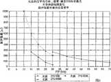
图6是一个在实施本发明时使用的激光脉冲能量以及脉冲重复频率之间的特征关系图。Figure 6 is a graph showing the characteristic relationship between laser pulse energy and pulse repetition frequency used in the practice of the present invention.
图7是一个在硅中的圆柱形开口的紫外线烧蚀图案的代表性图示。Figure 7 is a representative illustration of the UV ablation pattern of a cylindrical opening in silicon.
图8是一个在硅中的沟槽的紫外线烧蚀图案的代表性图示。Figure 8 is a representative illustration of the UV ablation pattern of a trench in silicon.
图9是一个在半导体材料中用来进行长切割的示例片段切割剖面的简化图。FIG. 9 is a simplified diagram of an example segmented cut profile for long cuts in semiconductor materials.
图10是一个在半导体材料中用来进行长切割的替代性片段切割剖面的简化图。Figure 10 is a simplified diagram of an alternative segment cut profile for long cuts in semiconductor materials.
图11是一个在半导体晶片中的MEMS元件的紫外线烧蚀图案的代表性图示。FIG. 11 is a representative illustration of a UV-ablated pattern of a MEMS device in a semiconductor wafer.
图12是一个制造在半导体晶片上的AWG元件的紫外线烧蚀图案代表性图示。Figure 12 is a representative illustration of the UV ablation pattern of an AWG component fabricated on a semiconductor wafer.
图13是一个紫外线透射的基座代表性图示,在半导体工件放置在该基座上用于使用紫外线烧蚀图案化方法来进行穿透处理。13 is a representative illustration of a UV transmissive susceptor upon which a semiconductor workpiece is placed for breakthrough processing using a UV ablation patterning method.
具体实施方式Detailed ways
图1展示硅的光学吸收是数作为波长的函数的图。参考图1,硅在紫外线波长展现非常快速上升的光学吸收。本发明的优势在于利用短于390纳米的激光波长,并且利用硅在紫外线中增加的吸收效能来有效地烧蚀硅,并因而直接地在硅中形成多种有用的图案或是特征。与在先技术中所教授的使用532纳米或是1064纳米的脉冲输出形成的特征比较相比,该吸收行为强烈地促进硅在紫外线的烧蚀性去除,并大量降低其热影响区域。Figure 1 shows a graph of the optical absorption of silicon as a function of wavelength. Referring to Figure 1, silicon exhibits very rapidly rising optical absorption at ultraviolet wavelengths. The advantage of the present invention is to utilize the laser wavelength shorter than 390nm and utilize the increased absorption efficiency of silicon in ultraviolet light to effectively ablate silicon and thus directly form various useful patterns or features in silicon. This absorption behavior strongly facilitates the ablative removal of silicon in UV light and greatly reduces its heat-affected zone compared to features formed using 532nm or 1064nm pulse output as taught in the prior art.
图2显示砷化镓的光学吸收是数作为波长的函数。参考图2,砷化镓在紫外线波长中显示一非常快速上升的光学吸收。砷化镓与硅在355纳米的吸收是数相当接近。砷化镓在光电子元件,例如二极管激光以及检测器中是一个关键性材料。Figure 2 shows the optical absorption of GaAs as a function of wavelength. Referring to Figure 2, Gallium Arsenide exhibits a very rapidly rising optical absorption in ultraviolet wavelengths. Gallium arsenide and silicon have fairly close absorption numbers at 355 nm. Gallium arsenide is a key material in optoelectronic components such as diode lasers and detectors.
图3以及图4展示各激光处理系统10a以及10b(通称为10)的替代性的较佳实施例,其使用具有晶片基座组件140的复合光束定位系统30,该组件可用于根据本发明的在半导体工件12中的紫外激光烧蚀微结构图案。参考图3以及图4,激光系统10的较佳实施例包含一个Q-开关式二极管泵浦(DP)的固态(SS)紫外激光14,其最好包含一种固态激光材料如Nd:YAG、ND:YLP、或是Nd:YVO4。激光14最好能够提供于波长为例如355纳米(三倍频Nd:YAG)、266纳米(四倍频Nd:YAG),或者是213纳米(五倍频Nd:YAG)且主要具有TEM00空间模态形态的一个或是多个以谐波方式产生的激光脉冲紫外激光输出16。3 and 4 illustrate an alternative preferred embodiment of each laser processing system 10a and 10b (generally 10) using a composite
虽然高斯形态可以用来说明激光输出16的幅照,然而熟习本项技术的人将了解到多数的激光14不会发射具有M2=1值的完美高斯输出16。为了方便起见,高斯这个术语在这里被用来包括M2小于或是等于约1.5时的形态,即使M2的值小于1.3或是1.2是较佳的。While a Gaussian shape can be used to illustrate the irradiance of the laser output 16, those skilled in the art will appreciate that most lasers 14 do not emit a perfectly Gaussian output 16 having a value ofM2 =1. For convenience, the term Gaussian is used herein to include morphologies whereM2 is less than or equal to about 1.5, even though values ofM2 less than 1.3 or 1.2 are preferred.
在一个较佳实施例中,激光14包含一个大约在355纳米操作的模型210-VO6的Q-开关式、三倍Nd:YAG激光,其在市面上可以从Lightwave电子公司取得。这个种激光已经使用在微型通孔钻孔系统ESI模式2700中,其可以在俄勒冈州波特兰市的电科学工业公司取得。在替代实施例中,一种可以在大约355纳米操作的Lightwave模式210-VO9的Q-开关式、三倍频Nd:YAG激光,以得到在高脉冲重复频率(PRF)时,每一脉冲具有高能量。熟知本技术的人将领会到其它的激光可以被使用而且其它的波长可以从其它列出的激光材料中得到。虽然激光空腔安排、谐波产生、Q-开关式操作,以及定位系统都是本领域的技术人员所公知的,但一些以上组件的特定细节将在较佳实施例的讨论中说明。In a preferred embodiment, laser 14 comprises a model 210-VO6 Q-switched, triple Nd:YAG laser operating at approximately 355 nm, which is commercially available from Lightwave Electronics. This type of laser has been used in the Micro Via Drilling System ESI Model 2700, available from Electro-Science Industries, Inc., Portland, Oregon. In an alternative embodiment, a Q-switched, tripled Nd:YAG laser in Lightwave mode 210-VO9 can be operated at about 355 nm to obtain a high pulse repetition frequency (PRF) of high energy. Those skilled in the art will appreciate that other lasers may be used and that other wavelengths may be derived from the other listed laser materials. While laser cavity arrangements, harmonic generation, Q-switched operation, and positioning systems are well known to those skilled in the art, specific details of some of the above components are set forth in the discussion of the preferred embodiments.
紫外线激光输出16选择性地通过几个的公知的放大以及/或是准直光学系统18,沿着一个光学路径20传播,然后由光束定位系统30导向,来将激光系统输出脉冲32射击到工件12上面想要射击的激光靶材位置34。光束定位系统30最好是包含一个传动平台定位器,其最好是使用至少两个横向平台36以及38,来支撑例如X、Y,以及/或是Z等几个定位镜42以及44,并且允许在相同的或者是不同的工件12上的几个靶材位置34之间快速移动The ultraviolet laser output 16 is selectively passed through several known amplifying and/or collimating optical systems 18, propagated along an
在一个较佳实施例中,传动平台定位器是一个分轴系统,其中,通常通过线型马达而沿着轨道46移动的Y平台36支撑并且移动工件12,而典型通过线型马达而沿着轨道48移动的X平台38是支撑并且移动一个快速定位器50以及相关的(多个)聚焦镜片。在X平台38以及Y平台36之间的Z维度也是可以调整的。定位镜42以及44将通过激光14以及快速定位器50之间的任何转弯对准光学路径20,其沿着光学路径20定位。举例来说,快速定位器50可以使用高分辨率线型马达或是一对检流计镜子,其可以基于提供的测试或是设计资料使单一或是反复的处理操作产生作用。平台36、38以及定位器50可以被控制,然后以独立或是协调的方式,以响应于预铸或者是未预铸的数据而一起移动。In a preferred embodiment, the drive stage positioner is a split-axis system in which the Y stage 36 supports and moves the
快速定位器50最好也包含一个视觉系统,其可以对准于在工件12表面上的一个或是多个支撑材(fiducial)。光束定位系统30可以使用传统的视觉或是光束来作用对准系统,这些系统经由物镜36或是与一个分离照相机来以离轴的方式来工作,这些是本领域的技术人员士所公知的。在一个实施例中,利用电子科学工业公司所销售的定位系统30中的使用Freedom library软件的HRVX视觉盒,来执行在激光系统10以及工件12上面的靶材位置34之间的对准。其它适用的对准系统在市面上是可取得的。对准系统最好是使用明亮视野、轴上照明,特别是对于镜面反射的工件如迭型或者是抛光型晶片。The
此外,光束定位系统30最好也使用非接触式的小位移传感器来决定由于平台36以及38的俯仰、偏向,或者是滚转造成的阿贝误差(Abbeerror),这些是不由轴位置指示器,例如线性尺度编码器或者是激光干涉仪所指示的。阿贝误差校正系统可以针对精确参考标准来进行校准,因此该校准只依赖于传感器中感受到的很小读数改变而不是依赖于传感器读数的绝对准确度。这种阿贝误差校正系统在2001年7月19日公开的第WO01/52004A1号的国际公开中以及在2001年10月18日,美国公开的第2001-0029674A1号公开中详细说明,Cutler的相对应的美国专利中请第09/755,950号所揭示的相关的部分在这里做为参考来结合。In addition, the
很多不同型式的定位系统30是熟知本技术的人士所公知的,而且一些定位系统30的实施例在Cutler等人的美国专利第5,751,585号中详细说明。一种可以从俄勒冈州波特兰市的电子科学工业公司中取得的微型通孔钻孔系统ESI模型5320是定位系统30的较佳实现,其已经用在电子工业中的树脂覆层铜封装激光钻孔中。其它的较佳定位系统例如在俄勒冈州波特兰市电子科学工业公司制造的第27xx、43xx、44xx,或者是53xx号模型序列也可以使用。使用X-Y线型马达来移动工件12以及使用X-Y平台来移动扫瞄透镜的一些系统对于进行长直线切割是具有生产成本效率(cost effective)的定位系统。本领域的技术人员士也将领会到以单一的X-Y平台来进行工件定位的系统,可以替代地使用,其是以一个固定的电子束定位(beam position)以及/或是固定式检流计来定位。本领域的技术人员将认知到这种系统可以被程序化以利用路径文件,路径文件(pathfile)将于高速度下动态地将聚焦的紫外线激光系统输出脉冲32定位,以产生多种有用的图案,其可以是周期性的或者是非周期性的。本领域的技术人员也将认识到,这种能力具有更多的优点而超越了Lee的经由投射成像配置来制作在硅中通孔的建议。Many different types of
一种选择性的激光功率控制器52,例如半波平板偏光器,可以沿着光学路径20定位。此外,一个或者是更多的光束检测组件54,例如光电二极管,可以是激光功率控制器52的下游,例如与适于对激光输出16的波长部分透射的定位镜44对准。光束检测组件54最好是与光束诊断电子组件连通,该电子组件传递信号以修改激光功率控制器52的作用。An optional laser power controller 52 , such as a half-wave plate polarizer, can be positioned along
参考图4,激光系统10b最好是使用至少两个激光14a以及14b,它们发射各别的激光输出16a以及16b,这些输出在横向方向是线性极化,而且分别沿光学路径20a及20b,分别朝着反射组件42a及42b传播。一个选择性的波平板56可以沿着光学路径20b放置。反射组件42a最好是一个极化敏感的光束结合器,并且沿着两个光学路径20a以及20b放置来结合激光输出16a以及16b以沿着共同的光学路径20传播。Referring to FIG. 4, laser system 10b preferably uses at least two lasers 14a and 14b that emit respective laser outputs 16a and 16b that are linearly polarized in the transverse direction and along optical paths 20a and 20b, respectively. Propagates toward reflective elements 42a and 42b. An optional wave plate 56 may be placed along the optical path 20b. Reflective assembly 42a is preferably a polarization sensitive beam combiner and is positioned along two optical paths 20a and 20b to combine laser outputs 16a and 16b for propagation along common
激光14a以及14b可以是相同或者不同型态的激光,并且可以产生具有相同或是不同波长的激光输出16a及16b。例如,激光输出16a可以是具有大约266纳米的波长,而激光输出16b可以是具有大约355纳米的波长。熟知本技术的人士将认识到到激光14a以及14b可以并排设置或者一个在另一个的上面,并且两者附着在传动平台36或38其中之一上。激光系统10b具有产生极高能量的激光输出脉冲32b的能力。在图4中显示的一个配置的特有优点是产生射击在工作表面、具有每脉冲增加能量的结合激光输出32,其在现有的单一激光头中很难产生。这种每脉冲增加能量用于烧蚀在厚硅晶片中很深的沟槽或是很深的圆柱形开口是特别具有优点的。Lasers 14a and 14b may be the same or different types of lasers and may produce laser outputs 16a and 16b having the same or different wavelengths. For example, laser output 16a may have a wavelength of approximately 266 nanometers, while laser output 16b may have a wavelength of approximately 355 nanometers. Those skilled in the art will recognize that the lasers 14a and 14b can be positioned side-by-side or one above the other, with both attached to one of the drive platforms 36 or 38 . Laser system 10b has the capability to generate extremely high energy laser output pulses 32b. A particular advantage of one configuration shown in FIG. 4 is to produce a combined laser output 32 that hits the work surface with increasing energy per pulse, which is difficult to produce in existing single laser heads. This increased energy per pulse is particularly advantageous for ablating deep trenches or deep cylindrical openings in thick silicon wafers.
尽管激光系统输出脉冲32基本上具有圆形形态,然而光束形状品质的改善可以以一种选择性的影像光学模块62达成,在其中不需要的光束假影,例如残余散光或者是椭圆的或是其它的形状特征是以空间方式过滤。参考图5,影像光学模块62最好是包含一个光学组件64、一个透镜66,以及一个放置在或是接近于光学组件64产生的光束腰部的光圈屏蔽68,以阻挡任何不想要的光束副叶以及周边部分,结果一个精确形状光点形态是实质地成像于在工作表面上。在较佳实施例中,光学组件64是一聚焦透镜,透镜66是一个准直镜组透镜,以增加激光系统10的构型弹性。Although the laser system output pulse 32 has a substantially circular shape, an improvement in the quality of the beam shape can be achieved with an optional imaging optics module 62 in which unwanted beam artifacts such as residual astigmatism are either elliptical or Other shape features are spatially filtered. Referring to FIG. 5, the image optics module 62 preferably includes an optical assembly 64, a lens 66, and an aperture shield 68 positioned at or close to the waist of the beam generated by the optical assembly 64 to block any unwanted beam secondary leaves. As well as peripheral parts, the result is a precisely shaped spot pattern that is substantially imaged on the work surface. In a preferred embodiment, the optical component 64 is a focusing lens, and the lens 66 is a collimator lens to increase the configuration flexibility of the
改变光圈的大小可以控制光点形态的周边鲜明度以产生一个较小,较鲜明的周边强度形态,如此可以提高对准的准确度。此外,以这种配置,光圈的形状可以是精确的圆形或者是改变为长方形、椭圆,或者是其它可以平行或者是垂直对准于一个切割方向的非圆形形状。屏蔽68的光圈可以选择性地在其光线射出侧向外散开。在影像光学模块62中,屏蔽68可以含有紫外线反射或者是紫外线吸收的材料,但最好是以介电材料例如紫外线级熔石英或是蓝宝石,以多层高紫外线反射覆层或将其它的紫外线光阻覆层予以覆层。本领域的技术人员士将领会到光圈屏蔽68可以在不使用光学组件64及66时使用。Changing the size of the aperture controls the peripheral sharpness of the spot shape to produce a smaller, sharper peripheral intensity shape, which improves alignment accuracy. Furthermore, with this configuration, the shape of the aperture can be precisely circular or altered to be rectangular, elliptical, or other non-circular shape that can be aligned parallel or perpendicular to a cutting direction. The aperture of shield 68 can optionally be diffused outwards on its light exit side. In imaging optics module 62, shield 68 may contain UV reflective or UV absorbing material, but is preferably made of a dielectric material such as UV grade fused silica or sapphire, with multiple layers of highly UV reflective coatings or other UV A photoresist coating is coated. Those skilled in the art will appreciate that aperture shield 68 can be used without optical assemblies 64 and 66 .
在替代的较佳实施例中,光学组件64包含一个或者是多个光束成形组件,其转换具有原始高斯幅照形态的激光脉冲为一较个具有近乎均匀的“顶帽式”成形(并且聚焦的)脉冲,或者特别是邻近于光学组件64下游光圈屏蔽68的一个超级高斯幅照形态。这种光束成形组件可以包含非球状光学或者是衍射光学组件。在一个较佳实施例中,透镜66包含用于控制光束大小以及发散的成像光学组件。本领域的技术人员士将领会到单一的成像透镜组件或是多重透镜组件可以被使用。本领域的技术人员士也将领会到成形激光输出可以在不使用光圈屏蔽68的时候使用。In an alternative preferred embodiment, optics assembly 64 includes one or more beam shaping assemblies that convert a laser pulse having an original Gaussian irradiance profile into a more nearly uniform "top-hat" shaped (and focused beam). ) pulse, or in particular a super-Gaussian irradiation pattern adjacent to the aperture shield 68 downstream of the optical assembly 64. Such beam shaping components may comprise aspheric optics or diffractive optics. In a preferred embodiment, lens 66 includes imaging optics for controlling beam size and divergence. Those skilled in the art will appreciate that a single imaging lens assembly or multiple lens assemblies can be used. Those skilled in the art will also appreciate that the shaped laser output can be used without the use of aperture shield 68 .
在一个较佳实施例中,光束的成形组件包含衍射光学组件(DOE),其可以以高效能及高准确度执行复杂的光束成形。光束成形组件不只转换高斯幅照形态成为一个接近均匀的幅照形态,它们也将成形输出聚焦到一个可决定的或者是特定的光点大小。虽然单一组件DOE是较佳,但本领域的技术人员士将领会到DOE可以包含由Dickey等人在美国专利第5,864,430号揭示的多重分离组件如相位盘以及转换组件,其也揭示用来做为光束成形目的的设计DOE的技术。上面讨论的成形以及成像技术在2000年12月7日发行的国际公开第WO00/73013号中有详细说明。申请于2000年5月26日,由Dunsky等人提出的相对应的美国专利申请第09/580,396号所揭示的相关的部分,在这并入参考。In a preferred embodiment, the beam shaping component includes a diffractive optical element (DOE), which can perform complex beam shaping with high performance and accuracy. Beam shaping components not only transform a Gaussian irradiance profile into a near-uniform irradiance profile, they also focus the shaped output to a determinable or specific spot size. While a single component DOE is preferred, those skilled in the art will appreciate that a DOE may contain multiple discrete components such as phase disks and switching components as disclosed by Dickey et al. in U.S. Patent No. 5,864,430, which is also disclosed for use as Techniques for designing DOEs for beam shaping purposes. The forming and imaging techniques discussed above are described in detail in International Publication No. WO00/73013, issued December 7,2000. Corresponding US Patent Application Serial No. 09/580,396, filed May 26, 2000, by Dunsky et al., is hereby incorporated by reference in relevant part.
为了达到提供每一脉冲能量的动力范围的弹性增加的目的,一个快速响应振幅控制机制,例如一种声光式调制器或者是电-光调制器被用来调制连续脉冲的脉冲能量。替代地,或与快速响应振幅控制机制结合,脉冲重复频率可以增加或是减少以产生连续脉冲的脉冲能量的改变。图6展示在实行本发明时,使用的激光14的脉冲能量以及脉冲重复频率(PRF)之间的特征关系。如图6所示,大于200微焦的脉冲能量可以从模型210-V06中得到。此外,也显示了,用于替代性激光如Lightwave210-VO9L以及Lightwave210-V09H的在脉冲能量和脉冲重复频率之间的特征关系。本领域的技术人员将领会到,图6对说明的要点是示例性的而且激光系统10的替代实施例将产生在脉冲能量和脉冲重复频率之间不同的特征关系。To provide an elastic increase in the dynamic range of each pulse energy, a fast-response amplitude control mechanism, such as an acousto-optic modulator or an electro-optic modulator, is used to modulate the pulse energy of successive pulses. Alternatively, or in combination with a fast response amplitude control mechanism, the pulse repetition frequency can be increased or decreased to produce a change in pulse energy for successive pulses. Figure 6 shows the characteristic relationship between the pulse energy of the laser 14 and the pulse repetition frequency (PRF) used in practicing the present invention. As shown in Figure 6, pulse energies greater than 200 microjoules can be obtained from model 210-V06. Furthermore, the characteristic relationship between pulse energy and pulse repetition frequency for alternative lasers such as Lightwave210-VO9L and Lightwave210-V09H is also shown. Those skilled in the art will appreciate that FIG. 6 is exemplary for the purposes of illustration and that alternative embodiments of
上面说明的紫外线激光系统10的性能特征可以被用来以半导体烧蚀方式,而且特别是对于硅,高速地形成微细尺度特征尺寸。这些特征尺寸包含,但不只限于穿透或是部分穿透硅晶片或其它的硅工件12的极高宽高比圆柱形开口100;形成穿透或者是部分地穿透的复杂几何形态的沟槽,以达到在硅晶片或者是硅工件12上面处理晶粒的切断目的;形成微细凸出特征尺寸以将在硅中形成的微型电路从母晶片中分开;AWG上面特征尺寸的形成以及/或是切断;以及在MEMS中特征尺寸的形成。此外,本发明促进无显著熔化边缘形成的特征尺寸、没有显著熔渣形成、以及没有显著特征尺寸边缘剥离形成的特征尺寸。The performance characteristics of the
图7是一个圆柱形的开口100的代表性图示,其是在硅工件12中由紫外线烧蚀图案所形成。该工件可以是,例如具有500微米厚度的本征硅基片70,其以0.5微米厚的二氧化硅钝化层覆盖(没有显示)。本领域的技术人员将理解到硅工件的厚度以及钝化层的厚度可以改变。FIG. 7 is a representative illustration of a
最好是通过在激光系统10的焦点平面中的位置定位硅工件12的靶材位置34,并且将一系列的激光系统输出脉冲32导引在硅工件12上面的靶材位置34,将圆柱形的开口100图案化。在这个实施例中,导引激光系统10在X以及Y轴方向移动硅工件12到一个计算机程序化的形心靶材位置34,该位置是圆柱形开口100的预定位置。连续的激光系统输出脉冲32的每一个是被入射到该程序化的形心靶材位置34上面。Preferably, by locating the target location 34 of the
以连续的重叠脉冲进行的烧蚀图案化,在这里称为硅工件的圆柱形开口100的冲孔,在包含每一脉冲的能量、脉冲重复频率(PRF)、以及聚焦光点大小的组合处理参数的较佳范围,对于有用的圆柱形开口100的快速冲孔的是特别有好处的。Ablation patterning with successive overlapping pulses, referred to herein as the punching of a
在冲孔过程中,当工件12固定在X以及Y轴位置时,连续的激光系统输出脉冲32分别入射到程序化的形心靶材位置34上面。对于该示例的硅的烧蚀图案化过程来说,每一脉冲的较佳能量范围大约是100微焦到1500微焦,比较好的是,每一脉冲能量的范围从大约200微焦到1000微焦,更好的是从大约300微焦到800微焦,最好是大约超过360微焦。较佳的脉冲重复频率范围大约在5千赫兹到100千赫兹之间,而且更好的是,脉冲重复频率的范围从大约7千赫兹到50千赫兹,并且最好是,脉冲重复频率范围从大约10千赫兹到30千赫兹。较佳聚焦光点的大小范围大约是1微米到25微米,更好的是,范围从大约3微米到20微米的一个聚焦光点大小,而且最好是,聚焦光点大小从大约8微米到15微米。本领域的技术人员将认知到,如显示在图6中的激光性能可以在如上面所说明的脉冲重复频率最佳范围中获得每一脉冲的输出能量。转到实际情况,以最佳过程参数运作的程序化ESI模型2700导致每秒一百个圆柱形开口的生产量,其中每一个圆柱形的开口在750微米厚硅晶片工件12的穿透冲孔的直径是35微米。During the punching process, when the
在另一个实施例中,激光聚焦位置的Z-高度以符合每一个后继的激光系统输出脉冲32的方式同时被移动,以将激光聚焦在硅工件12中连续更深的位置中,藉此将聚焦光点维持在与剩余硅表面更一致的位置中。In another embodiment, the Z-height of the laser focus position is simultaneously shifted in a manner consistent with each subsequent laser system output pulse 32 to focus the laser in successively deeper positions in the
在一个较佳实施例中,圆柱形开口100完全穿透工件12的整个厚度102,其是使用大于300微焦耳(μJ),以大约100个连续的激光系统输出脉冲32的激光14的输出脉冲能量来完成。激光系统输出脉冲32以一个大约12微米直径的聚焦光点大小(1/e2)入射到工作表面上。在这个实施例中产生的圆柱形开口100通常具有大约20微米的上表面开口直径(dt)104以及大约13微米的出口直径(db)106,因此产生了大约30∶1的宽高比以及以0.4°的逐渐变细开口角度的这种通孔圆柱形开口。In a preferred embodiment, the
本领域的技术人员将进一步的领会到有效地产生穿透硅的高品质圆柱形开口100所须的每一脉冲精确能量值、聚焦光点大小、以及脉冲的数量,可以随着硅工件12的厚度102、相对的厚度、覆盖层的组成而变化,其中二氧化硅只是一个例子,而且亦根据使用精确的紫外线波长而定。例如,为了在硅中产生通孔圆柱形开口100,以做为硅晶粒上面图案化集成电路至印刷电路的直接导电互连线路的位置,该硅可以是例如只有50微米的厚度。在这个示例中,使用大约只有很少的十个脉冲扫瞄来产生想得的通孔圆柱形开口100。本领域的技术人员将了解到不完全穿透硅的整个厚度102的圆柱形的开口,可以经由上述的正确参数选择来产生。Those skilled in the art will further appreciate that the precise amount of energy per pulse, focused spot size, and number of pulses necessary to effectively produce a high-quality
本领域的技术人员将领会到这种具有穿过硅的高宽高比以及非常小的锥形角的圆柱形开口100,对于电子封装以及互连应用是非常具有优点的。此外,一个或是更多群的这些小通孔圆柱形开口100可以被放置在接近工件12、电路或是晶粒周边的顶端,或是在标记、切片、或是切割道或是它们的交叉点之中,使得工件12的背部或是底边可以精确地对准于顶端的特征尺寸。这种对准促进背部处理例如激光标记或者是切割以提高处理速度或是品质。用在前面以及/或是背面的晶片切片或是切割技术是于下列的专利案之中被更详细讨论:2001年3月9日申请的第09/803,382号,标题为“例如陶瓷或玻璃的易碎的、高融化温度的靶材的紫外线激光切割或是形态修改”美国专利申请,以及2001年6月28日申请的第60/301,701号,标题为“具有表面组件层的晶片切割或是钻孔的多重步骤激光处理”的美国临时专利申请。Those skilled in the art will appreciate that such a
图8是一个硅工件12中的沟槽110的紫外线烧蚀图案化代表性图标。沟槽110的图案化最好是通过将硅工件12定位在激光系统10的焦点平面上,并通过当激光定位系统30沿着工件12的X-以及/或是Y-轴移动工件12时,将一连串相继重叠的激光系统输出脉冲32导引到硅工件12上。FIG. 8 is a representative diagram of UV ablation patterning of
对于在硅中形成沟槽的烧蚀图案化过程,每一脉冲的较佳能量范围大约是在100微焦到1500微焦之间,而且最好是,每一脉冲的能量大约200微焦到1000微焦范围,更好的是从大约300微焦到800微焦且最好是超过大约360微焦。较佳脉冲重复频率范围大约是5千赫兹到于100千赫兹,而且更好的是,脉冲重复频率范围从大约7千赫兹到50千赫兹,而最好的是,从大约10千赫兹到30千赫兹。较佳的聚焦光点大小范围大约是从1微米到25微米,而且更好的是,聚焦光点大小范围从大约3微米到20微米,而最好的是,从大约8微米到15微米。该较佳的很小尺寸范围是大约0.1微米到10微米,较好的是,很小的尺寸范围从到大约0.3微米到5微米,而最好是很小的从大约0.5微米到3微米。该很小的尺寸可以通过激光束定位系统的一个或是两个平台速度控制来调整以及通过协调移动速度与脉波重复频率以及激光发射的方式来调整。For the ablation patterning process for forming trenches in silicon, the preferred energy range per pulse is between approximately 100 microjoules and 1500 microjoules, and most preferably, the energy per pulse is approximately 200 microjoules to The range of 1000 microjoules, more preferably from about 300 microjoules to 800 microjoules and more preferably in excess of about 360 microjoules. Preferably, the pulse repetition frequency ranges from about 5 kHz to 100 kHz, and more preferably, the pulse repetition frequency ranges from about 7 kHz to 50 kHz, and most preferably, from about 10 kHz to 30 kHz. kilohertz. A preferred focused spot size ranges from about 1 micron to 25 microns, and more preferably a focused spot size ranges from about 3 microns to 20 microns, and most preferably, from about 8 microns to 15 microns. The preferred small size range is from about 0.1 micron to 10 microns, more preferably the small size range is from about 0.3 micron to 5 microns, and most preferably the small size is from about 0.5 micron to 3 microns. This small size can be adjusted by one or two stage speed controls of the laser beam positioning system and by coordinating the movement speed with pulse repetition rate and laser emission.
在一个较佳实施例中,通过使用从激光14的大约360微焦脉冲能量输出,并以10毫米/秒的平台速率在180道(passes)内在工件12上的1微米很小的尺寸(bite size),线性沟槽110被完全切割穿透覆盖有2.0微米二氧化硅钝化层的750微米厚的本征硅。这些激光脉冲以直径12微米的聚焦光点大小(1/e2)入射在该工作表面。本领域的技术人员将认知到各种不同几何形态的不同图案,包含但不限于,正方形、长方形、椭圆型、螺旋形、以及/或是组合的几何形态,可以经由激光系统10所使用的工具路径档案程序化以及在处理期间沿着X及Y-轴定位硅工件12的定位系统30来产生。至于激光切割,光束定位系统30最好是对准于习知的典型切割机切割或是其它的基准点或是晶片表面上的图案。如果该晶片是已经以机械方式被刻痕,则最好以对准切割边缘来克服切割机的容限度以及对准错误。In a preferred embodiment, the 1 micron bite size (bite) on the
激光切割比机械切割(约300微米的切割道以及约150微米的切割路径)显著地破坏较少的材料(小于50微米宽且最好小于25微米宽的切口),因此在晶片上面的组件可以以更靠近的方式制造,允许更多的组件在每一个晶片上产生。因此,激光切割过程将列之间的间距以及在组件之间的间距降至最低。Laser dicing destroys significantly less material (kerfs less than 50 microns wide and preferably less than 25 microns wide) than mechanical cutting (about 300 microns of scribe and about 150 microns of cutting path), so components on the wafer can Manufacturing in closer proximity allows more components to be produced per wafer. Thus, the laser cutting process minimizes the spacing between columns as well as between components.
机械切割的除去也可以简化工件12中的组件制造。特别是,机械切割可分配显著的机械应力到组件上以使它们从它们的载具脱离。为了避免列遗失,组件制造可以在列以及载具之间使用强胶着剂或者是环氧化物。全激光过程显著地降低了用来将列固定在载具上面的胶着剂的机械强度要求。因此,激光切割便不需用到固定列到载具的强胶着剂或是环氧化物以及不需用到除去它们所需的剧烈化学药品。反而,胶着剂可以选来减缓松脱,例如减少松脱时间以及减少暴露于潜在的腐蚀性化学药品中,而且对于UV激光过程的顺从性来说,大量地降低组件损伤的风险,也因此提高产出。The removal of mechanical cuts may also simplify the fabrication of components in
激光列切片降低列弯曲,因为激光切片不会施加如机械切片这么多的机械压力。然而,如果列弯曲或是其它的列缺陷是明显的,该列可以以激光切块(以及再切片)来弥补这些缺陷,而无须关心关键组件在列之间用来进行做机械切块所需的组件对准。为了方便起见,(穿透)切割这个术语可以广泛地用来包含切片(通常与晶片列分割有关)或是切割(经常与从晶片列分件隔离有关),以及切片与切割可以互换地被用在本发明的内容中。Laser column slicing reduces column bowing because laser slicing does not exert as much mechanical stress as mechanical slicing. However, if column bowing or other column defects are evident, the column can be laser diced (and re-diced) to compensate for these defects, regardless of the need for critical components to be mechanically diced between columns. components are aligned. For convenience, the term (through) dicing can be used broadly to include either dicing (often associated with separation of wafer columns) or dicing (often associated with isolation from wafer columns), and dicing and dicing are interchangeably referred to as used in the context of the present invention.
因为定位系统30可以对准通孔100或者是基准点,因此激光系统10可以独立地处理每一个列以及/或是每一个组件。对于斜列,激光光点可以在适当位置执行横跨斜列的横向切割,该适当位置是相对于组件的外边缘而言,其在每一个切割之间具有平台以及/或是光束传动,以产生想要的长方形或是曲线的波形图案。因此,激光切割可以补偿列固定的缺陷并且或许可节省机械切割所毁坏的整个列组件。Because the
通过将长的切割路径分为短的片段,可改善紫外线激光切割穿透硅及相似材料的产出。例如,对于较厚的硅的穿透切割或者是沟槽切割来说,这些片段最好是从大约10微米到1公厘到,更好的是从约100微米到1000微米,而最好是从大约200微米到500微米。激光束是在一个第一短片段内以一个预定次数通过而扫瞄,然后被移动并在一个第二短片段之中以一个预定次数通过而扫瞄。该很小的尺寸、片段尺寸、以及片段重叠可以被操控以将沟槽填满的数量以及型态最小化。The yield of UV laser cutting through silicon and similar materials is improved by breaking long cutting paths into short segments. For example, for thicker silicon through cutting or trench cutting, the segments are preferably from about 10 microns to 1 mm, more preferably from about 100 microns to 1000 microns, and most preferably From about 200 microns to 500 microns. The laser beam is scanned with a predetermined number of passes in a first short segment, and then moved and scanned with a predetermined number of passes in a second short segment. The small size, segment size, and segment overlap can be manipulated to minimize the amount and pattern of trench fills.
图9描绘出一个示例片段切割形态112a的简化表示方式。参考图9,切割形态112a被显示,为了方便,其具有从左到右的路径切割方向以及具有从右到左形成的分离切割片段116k1-116r3(通称为切割片段116)。虽然切割片段116k1-116r3为了方便在图9之中以平行的方式描绘,但切割片段116k1-116r3实际上是在同一在线的。图9描绘出多重片段集合114a,其每一个包含一个起始片段116k以及多重的逐渐增长重叠片段116m-116r,其最好是以字母顺序处理。最好是,每一个集合114a在下一个集合被处理之前被处理到选定的中间深度或者是完全穿透切割。虽然每一个集合114a只有5个重叠片段被显示,但本领域的技术人员士将领会到实际更大数量的重叠片段116可以被使用,特别是当需要来配合靶材材料厚度的时,可增加较小的增量长度。本领域的技术人员士也将领会到任何或者是所有在切割形态112a之中的使用片段116可以在两个方向被处理,而不是如图9显示的单一方向。FIG. 9 depicts a simplified representation of an example segment cut configuration 112a. Referring to FIG. 9 , a cutting pattern 112a is shown, for convenience, with a path cutting direction from left to right and with separate cutting segments 116k1 -116r3 (collectively, cutting segments 116 ) formed from right to left. Although the cutting segments 116k1 - 116r3 are depicted in parallel in FIG. 9 for convenience, the cutting segments 116k1 - 116r3 are actually on the same line. FIG. 9 depicts a set of multiple segments 114a, each comprising a starting segment 116k and multiple progressively growing overlapping segments 116m-116r, which are preferably processed in alphabetical order. Preferably, each set 114a is processed to a selected intermediate depth or a full penetration cut before the next set is processed. Although only 5 overlapping segments per set 114a are shown, those skilled in the art will appreciate that a substantially larger number of overlapping segments 116 may be used, especially as needed to match the thickness of the target material. Smaller increment length. Those skilled in the art will also appreciate that any or all of the used segments 116 in the cutting configuration 112a can be processed in two directions rather than a single direction as shown in FIG. 9 .
图10描绘出一种示例片段切割形态112b的简化表示方式,其多多少少是相似于形态112a的。参考图10,形态112b与形态112a是以相同片段集合114做为开始。然而,片段集合114b省略片段116k并且逐渐地与事先被处理的片段集合达到60%的重叠。在一个这个种实施例的示例中,片段116k1以30次通过切割并且具有200微米的长度。然后,片段116m1以6次通过(30次通过的1/5)切割并且具有240微米的长度(200微米加上片段116k1长度的1/5)。然后,片段116n1以6次通过切割并且具有280微米的长度(200微米加上片段116k1长度的2/5)。这个种序列被继续直到给定片段集合114b被完成。这个种示例可以展现大于或是等于8.5厘米/分的切割速度。FIG. 10 depicts a simplified representation of an example segment cut configuration 112b, which is somewhat similar to configuration 112a. Referring to FIG. 10 , the modality 112b and the modality 112a start with the same segment set 114 . However, segment set 114b omits segment 116k and gradually reaches 60% overlap with the previously processed segment set. In an example of one such embodiment, segment 116k1 is cut with 30 passes and has a length of 200 microns. Fragment 116m1 was then cut in 6 passes (1/5 of 30 passes) and had a length of 240 microns (200 microns plus 1/5 of the length of fragment 116k1 ). Fragment 116n1 is then cut in 6 passes and has a length of 280 microns (200 microns plus 2/5 of the length of fragment 116k1 ). This seed sequence is continued until the given fragment set 114b is completed. Such an example may exhibit a cutting speed greater than or equal to 8.5 cm/min.
实时监测也可以被用来将已经完成切割的切割路径的再扫瞄部分降低。此外,激光束的极化方向可以与切割方向相互关联以进一步提高生产。这些片段切割技术在2001年6月8日申请的第60/297,218号且标题为”激光片段切片或切割”的美国临时专利申请中被详细讨论。Real-time monitoring can also be used to reduce rescanned portions of the cut path where cuts have already been made. In addition, the polarization direction of the laser beam can be correlated with the cutting direction to further improve production. These segment cutting techniques are discussed in detail in US Provisional Patent Application Serial No. 60/297,218, filed June 8, 2001, and entitled "Laser Fragment Slicing or Cutting."
本紫外线烧蚀图案化方法的另一个应用是用来产生微机电系统(MEMS)组件120。图11是一个MEMS组件120的紫外线烧蚀图案化的代表性图。在一个较佳实施例之中,是使用上面所说明的方法来使MEMS组件120图案化,以在硅中产生沟槽122a、122b、122c、122d以及122e(通称为沟槽122)。本领域的技术人员士将领会到经由激光定位系统30的X以及/或是Y轴的计算机控制,该导向激光系统输出脉冲32可以被导引到工作表面,使得重叠脉冲产生一个表达任何复杂曲线几何形态的图案。这种结合紫外线烧蚀图案化方法的能力可以被用来产生在硅中复杂曲线的几何图案,其对于多种AWG组件120的有效生产是很有用的。Another application of the present UV ablation patterning method is to create microelectromechanical systems (MEMS) components 120 . FIG. 11 is a representative diagram of UV ablation patterning of a MEMS component 120 . In a preferred embodiment, MEMS device 120 is patterned using the methods described above to create trenches 122a, 122b, 122c, 122d, and 122e (collectively trenches 122) in the silicon. Those skilled in the art will appreciate that via computer control of the X and/or Y axes of the
本紫外线烧蚀图案化方法的另一个应用是处理光学集成电路,例如在半导体晶片工件12上面产生一种数组波导光栅(AWG)组件130。图12是一个AWG组件130的紫外线烧蚀图案化的代表性图标。在一个较佳实施例中,是使用上面所说明的方法将AWG 130图案化,以产生曲线沟槽132,例如具有在硅中的132a、132b、132c、132d,以及132e部分。虽然沟槽132被显示为对称的,本领域的技术人员士将领会到经由激光定位系统30的X以及/或是Y轴的计算机控制,该导向激光系统输出脉冲32可以被导引到工作表面,使得重叠脉冲32产生一个表达任何复杂曲线形态或是几何形态的图案。这种结合紫外线烧蚀图案化方法的能力可以被用来产生在硅中的复杂曲线几何图案,其对于多种AWG组件130的有效生产是很有用的。Another application of the present UV ablation patterning method is in the processing of optical integrated circuits, such as the creation of an array waveguide grating (AWG) assembly 130 on a
以传统金属例如铝制造的基座的使用,对于穿透处理硅工件12是不具优点的,因为这些传统金属材料在紫外线的高反射可以造成硅工件12背部的损伤。实验显示出的显著证据为,在圆柱形的通孔开口100或者是穿透沟槽110周围,在穿透处理完成之后,从金属基座顶端反射的能量所造成的背部损伤。然而,在圆柱形通孔开口100或是穿透沟槽110的附近则没有发现背部损伤,这些在基座顶端中的整个修整孔上是被易于发现地钻穿。。The use of susceptors made of conventional metals such as aluminum is not advantageous for through-processing the
图13是基座组件140的代表性图式,硅工件12最好是被放置在其上面,以使用紫外线烧蚀图案化方法进行穿透处理。基座组件140最好是包含一个真空基座142、一个基座顶端144、以及一个选择性的保持载具146。基座142是最好是以传统金属材料制作而且最好是拴到一个额外的平板148。平板148是用来简单地连接至平台36或者是38中的至少一个以及从其脱离的。接合机制最好是机械式而且可以包含对接的沟槽以及隆起及可以包含一个锁定机制。本领域的技术人员士将领会到很多种精确的对准及锁定以及键的机制是可能的。本领域的技术人员士也将领会到该基座142可以替代地用以直接固定于平台36或是38。FIG. 13 is a representative drawing of a susceptor assembly 140 upon which a
基座顶端144最好是以介电材料制造,其在选定做为特别的图案化应用的紫外线波长时具有较低的反射率。在一个使用由三倍频,Q-开关式二极管泵浦ND:YAG激光的355微米波长输出的较佳实施例中,紫外线可穿透的基座顶端144是以紫外线级或者是准分子激光级熔融石英、MgF2、或者是CaF2所制造。在另一个实施例中,紫外线可穿透的基座顶端144可以替代地或是额外地以液体冷却,以协助维持硅工件12的温度稳定性。本领域的技术人员将认知到熔融石英是一种紫外线可穿透的材料,其是由氧化非晶硅所组成,并且是以硅以及氧的化学结合所形成的。Susceptor top 144 is preferably fabricated from a dielectric material that has low reflectivity at the ultraviolet wavelength selected for the particular patterning application. In a preferred embodiment using a frequency tripled, Q-switched diode-pumped ND:YAG laser with a wavelength output of 355 microns, the UV-transparent pedestal tip 144 is manufactured with UV-grade or excimer laser-grade Made of fused silica, MgF2, or CaF2. In another embodiment, the UV transparent pedestal tip 144 may alternatively or additionally be liquid cooled to assist in maintaining the temperature stability of the
再次参考图13,一个保持载具146可以被放置在基座顶端144上面,以达到支撑硅工件12的目的以及将它在经紫外线烧蚀图案化后扣住。保持载具146也最好是以一种紫外线可穿透的材料制造,以防止背部反射损伤到穿孔处理的工件12。保持载具146最好经加工以包含浅空腔式,以使得被处理的硅工件12在穿透处理操作后稳固在其中。Referring again to FIG. 13 , a holding carrier 146 may be placed on top of the pedestal top 144 for the purpose of supporting the
在一个替代实施例中,基座顶端144或是保持载具146可以以一种紫外线吸收材料制造,例如铝或是铜,以使得激光系统10可以使用将浅空腔图案的工具路径档案,该空腔是被钻入工件12之中来将对应的图案切割成基座顶端144或是保持载具146的材料。该空腔可以是,例如对应于要被钻的孔洞或是边缘图案并且在穿孔切割过程中防止工件12的背部受到损伤。此外,任何从过程产生的残渣可以沈淀到远离工件12背部的空腔中。在一个较佳实施例中,浅空腔的图案是经处理为具有稍为大于对应的工件12被处理后的尺寸,因此使被处理后的工件12可被固定安置于保持载具146的空腔中。在一个替代实施例中,保持载具146是以紫外线可穿透的材料以替代的例如光学制造或者是蚀刻方式制造,并且被接序地对准以及固定在基座顶端144上面。基座组件140的这些实施例在其它材料例如聚酰胺的紫外线通孔钻孔中也具有一些有用的应用。In an alternate embodiment, the pedestal tip 144 or the holding carrier 146 can be fabricated from a UV absorbing material, such as aluminum or copper, so that the
本领域的技术人员将认识到净化气体,例如氮、氩、氦,以及干空气,可以被有用地用来协助从工件12中去除废弃的烟气。可以使用附着在激光系统10的传送头来将这种净化气体传送到非常靠近工作表面的附近区域。Those skilled in the art will recognize that purge gases, such as nitrogen, argon, helium, and dry air, may be usefully used to assist in the removal of waste fumes from
为了使用紫外线烧蚀图案方法来改善处理的硅工件12的表面品质,被处理的工件12可以使用超音波浴在液体中清洗,该液体包括但不限于水、丙酮、甲醇、以及乙醇。本领域的技术人员将认识到洗净在氢氟酸中处理的硅工件12,在去除不需要的氧化层时可以是很有帮助的。To improve the surface quality of the treated
虽然上面提供的说明主要是针对处理硅以及砷化镓,但所说明的方法也通常可应用于其它可用做工件12的基片70的半导体,例如碳化硅、氮化硅,或者是磷化铟。Although the description provided above is primarily directed to processing silicon and gallium arsenide, the methods described are also generally applicable to other semiconductors that may be used as the
对本领域的技术人员来说,很明显的,在不脱离本发明的依据原理前提下,可以改变上面所说明的本发明实施例细节。因此,本发明的范围应由权利要求书界定。It is obvious to those skilled in the art that the details of the embodiments of the present invention described above can be changed without departing from the principle of the present invention. Therefore, the scope of the present invention should be defined by the appended claims.
Claims (44)
Translated fromChineseApplications Claiming Priority (5)
| Application Number | Priority Date | Filing Date | Title |
|---|---|---|---|
| US60/256,556 | 2000-12-18 | ||
| US26555601P | 2001-01-31 | 2001-01-31 | |
| US60/265,556 | 2001-01-31 | ||
| US09/803,382 | 2001-03-09 | ||
| US09/803,382US20020033558A1 (en) | 2000-09-20 | 2001-03-09 | UV laser cutting or shape modification of brittle, high melting temperature target materials such as ceramics or glasses |
Publications (2)
| Publication Number | Publication Date |
|---|---|
| CN1527754A CN1527754A (en) | 2004-09-08 |
| CN1301178Ctrue CN1301178C (en) | 2007-02-21 |
Family
ID=26951292
Family Applications (1)
| Application Number | Title | Priority Date | Filing Date |
|---|---|---|---|
| CNB028044045AExpired - Fee RelatedCN1301178C (en) | 2001-01-31 | 2002-01-10 | Patterning of Microstructures in Semiconductors by Ultraviolet Laser Ablation |
Country Status (7)
| Country | Link |
|---|---|
| EP (1) | EP1365880A4 (en) |
| JP (1) | JP4634692B2 (en) |
| CN (1) | CN1301178C (en) |
| CA (1) | CA2436736A1 (en) |
| GB (1) | GB2389811B (en) |
| TW (1) | TW525240B (en) |
| WO (1) | WO2002060636A1 (en) |
Cited By (1)
| Publication number | Priority date | Publication date | Assignee | Title |
|---|---|---|---|---|
| CN102672347A (en)* | 2011-03-10 | 2012-09-19 | 株式会社迪思科 | Laser processing device |
Families Citing this family (22)
| Publication number | Priority date | Publication date | Assignee | Title |
|---|---|---|---|---|
| US6676878B2 (en) | 2001-01-31 | 2004-01-13 | Electro Scientific Industries, Inc. | Laser segmented cutting |
| US6949449B2 (en) | 2003-07-11 | 2005-09-27 | Electro Scientific Industries, Inc. | Method of forming a scribe line on a ceramic substrate |
| US7985942B2 (en)* | 2004-05-28 | 2011-07-26 | Electro Scientific Industries, Inc. | Method of providing consistent quality of target material removal by lasers having different output performance characteristics |
| CN100591458C (en)* | 2004-09-29 | 2010-02-24 | 三菱麻铁里亚尔株式会社 | Laser processing method and laser processing device |
| US20060108327A1 (en)* | 2004-11-23 | 2006-05-25 | Chng Kiong C | Method of manufacturing a microstructure |
| DE102005042072A1 (en)* | 2005-06-01 | 2006-12-14 | Forschungsverbund Berlin E.V. | Vertical electrical contact connections e.g. micro-vias, producing method for silicon carbide-wafer, involves laser boring of passage holes through wafer and active layers and applying antiwetting layer in area of openings of holes |
| JP2007067082A (en)* | 2005-08-30 | 2007-03-15 | Disco Abrasive Syst Ltd | Wafer drilling method |
| DE102005042074A1 (en) | 2005-08-31 | 2007-03-08 | Forschungsverbund Berlin E.V. | Method for producing plated-through holes in semiconductor wafers |
| US7767595B2 (en)* | 2006-10-26 | 2010-08-03 | Semiconductor Energy Laboratory Co., Ltd. | Manufacturing method of semiconductor device |
| CN101041415B (en)* | 2006-11-07 | 2010-08-11 | 东南大学 | Method for making nano hole on silicon chip |
| JP2008155274A (en)* | 2006-12-26 | 2008-07-10 | Disco Abrasive Syst Ltd | Wafer processing method |
| KR101041140B1 (en)* | 2009-03-25 | 2011-06-13 | 삼성모바일디스플레이주식회사 | Substrate Cutting Method |
| CN101850981A (en)* | 2010-06-23 | 2010-10-06 | 东北林业大学 | A method for preparing silicon oxide nanofoam by laser ablation |
| TWI587957B (en)* | 2011-08-18 | 2017-06-21 | 奧寶科技有限公司 | A lens assembly for use in an inspection/repair/inspection system for electrical circuits and a combiner assembly for use in an inspection/repair/inspection system for electrical circuits |
| CN102956239A (en)* | 2011-08-29 | 2013-03-06 | 新科实业有限公司 | Heads, HGAs, and Disk Drive Units |
| CN103567642B (en)* | 2012-08-08 | 2017-07-11 | 赛恩倍吉科技顾问(深圳)有限公司 | Sapphire cutter sweep |
| CN103962727B (en)* | 2013-01-28 | 2018-03-02 | 深圳市裕展精密科技有限公司 | Sapphire cutter device |
| US10118250B1 (en) | 2017-09-15 | 2018-11-06 | International Business Machines Corporation | In-situ laser beam position and spot size sensor and high speed scanner calibration, wafer debonding method |
| CN108326435B (en)* | 2017-12-29 | 2022-08-30 | 大族激光科技产业集团股份有限公司 | Laser marking method for die steel |
| CN108637472B (en)* | 2018-06-05 | 2023-12-08 | 昆山宝锦激光拼焊有限公司 | Skylight laser welding line platform |
| CN108637473B (en)* | 2018-06-05 | 2023-12-08 | 昆山宝锦激光拼焊有限公司 | One-time positioning welding forming device for skylight plate |
| IT201900006740A1 (en)* | 2019-05-10 | 2020-11-10 | Applied Materials Inc | SUBSTRATE STRUCTURING PROCEDURES |
Citations (7)
| Publication number | Priority date | Publication date | Assignee | Title |
|---|---|---|---|---|
| US4534804A (en)* | 1984-06-14 | 1985-08-13 | International Business Machines Corporation | Laser process for forming identically positioned alignment marks on the opposite sides of a semiconductor wafer |
| CN1142743A (en)* | 1995-08-07 | 1997-02-12 | 三菱电机株式会社 | Circuit board laser processing method and processing device thereof, and carbon dioxide laser oscillator |
| US5751585A (en)* | 1995-03-20 | 1998-05-12 | Electro Scientific Industries, Inc. | High speed, high accuracy multi-stage tool positioning system |
| US5841099A (en)* | 1994-07-18 | 1998-11-24 | Electro Scientific Industries, Inc. | Method employing UV laser pulses of varied energy density to form depthwise self-limiting blind vias in multilayered targets |
| JPH11245071A (en)* | 1998-03-02 | 1999-09-14 | Sumitomo Heavy Ind Ltd | Laser processing device |
| US6032997A (en)* | 1998-04-16 | 2000-03-07 | Excimer Laser Systems | Vacuum chuck |
| US6057180A (en)* | 1998-06-05 | 2000-05-02 | Electro Scientific Industries, Inc. | Method of severing electrically conductive links with ultraviolet laser output |
Family Cites Families (13)
| Publication number | Priority date | Publication date | Assignee | Title |
|---|---|---|---|---|
| US4473737A (en)* | 1981-09-28 | 1984-09-25 | General Electric Company | Reverse laser drilling |
| JP2621599B2 (en)* | 1990-07-05 | 1997-06-18 | 日本電気株式会社 | Contact hole forming apparatus and method |
| US5611946A (en)* | 1994-02-18 | 1997-03-18 | New Wave Research | Multi-wavelength laser system, probe station and laser cutter system using the same |
| US5847960A (en)* | 1995-03-20 | 1998-12-08 | Electro Scientific Industries, Inc. | Multi-tool positioning system |
| JPH11773A (en)* | 1997-06-11 | 1999-01-06 | Nec Corp | Laser beam machine and its method |
| JP3532100B2 (en)* | 1997-12-03 | 2004-05-31 | 日本碍子株式会社 | Laser cleaving method |
| US6063695A (en)* | 1998-11-16 | 2000-05-16 | Taiwan Semiconductor Manufacturing Company | Simplified process for the fabrication of deep clear laser marks using a photoresist mask |
| JP2000164535A (en)* | 1998-11-24 | 2000-06-16 | Mitsubishi Electric Corp | Laser processing equipment |
| TW482705B (en)* | 1999-05-28 | 2002-04-11 | Electro Scient Ind Inc | Beam shaping and projection imaging with solid state UV Gaussian beam to form blind vias |
| US6472295B1 (en)* | 1999-08-27 | 2002-10-29 | Jmar Research, Inc. | Method and apparatus for laser ablation of a target material |
| US6255621B1 (en)* | 2000-01-31 | 2001-07-03 | International Business Machines Corporation | Laser cutting method for forming magnetic recording head sliders |
| US6356337B1 (en)* | 2000-03-08 | 2002-03-12 | Anvik Corporation | Two-sided substrate imaging using single-approach projection optics |
| DE10026066A1 (en)* | 2000-05-25 | 2001-11-29 | Deere & Co | Device for wrapping a round bale |
- 2002
- 2002-01-10EPEP02707453Apatent/EP1365880A4/ennot_activeWithdrawn
- 2002-01-10WOPCT/US2002/000867patent/WO2002060636A1/enactiveApplication Filing
- 2002-01-10CNCNB028044045Apatent/CN1301178C/ennot_activeExpired - Fee Related
- 2002-01-10GBGB0317853Apatent/GB2389811B/ennot_activeExpired - Fee Related
- 2002-01-10JPJP2002560818Apatent/JP4634692B2/ennot_activeExpired - Fee Related
- 2002-01-10TWTW091100223Apatent/TW525240B/ennot_activeIP Right Cessation
- 2002-01-10CACA002436736Apatent/CA2436736A1/ennot_activeAbandoned
Patent Citations (7)
| Publication number | Priority date | Publication date | Assignee | Title |
|---|---|---|---|---|
| US4534804A (en)* | 1984-06-14 | 1985-08-13 | International Business Machines Corporation | Laser process for forming identically positioned alignment marks on the opposite sides of a semiconductor wafer |
| US5841099A (en)* | 1994-07-18 | 1998-11-24 | Electro Scientific Industries, Inc. | Method employing UV laser pulses of varied energy density to form depthwise self-limiting blind vias in multilayered targets |
| US5751585A (en)* | 1995-03-20 | 1998-05-12 | Electro Scientific Industries, Inc. | High speed, high accuracy multi-stage tool positioning system |
| CN1142743A (en)* | 1995-08-07 | 1997-02-12 | 三菱电机株式会社 | Circuit board laser processing method and processing device thereof, and carbon dioxide laser oscillator |
| JPH11245071A (en)* | 1998-03-02 | 1999-09-14 | Sumitomo Heavy Ind Ltd | Laser processing device |
| US6032997A (en)* | 1998-04-16 | 2000-03-07 | Excimer Laser Systems | Vacuum chuck |
| US6057180A (en)* | 1998-06-05 | 2000-05-02 | Electro Scientific Industries, Inc. | Method of severing electrically conductive links with ultraviolet laser output |
Cited By (2)
| Publication number | Priority date | Publication date | Assignee | Title |
|---|---|---|---|---|
| CN102672347A (en)* | 2011-03-10 | 2012-09-19 | 株式会社迪思科 | Laser processing device |
| CN102672347B (en)* | 2011-03-10 | 2015-09-23 | 株式会社迪思科 | Laser processing device |
Also Published As
| Publication number | Publication date |
|---|---|
| GB2389811B (en) | 2004-10-27 |
| CN1527754A (en) | 2004-09-08 |
| EP1365880A4 (en) | 2008-04-16 |
| GB2389811A (en) | 2003-12-24 |
| JP4634692B2 (en) | 2011-02-16 |
| JP2004526575A (en) | 2004-09-02 |
| CA2436736A1 (en) | 2002-08-08 |
| WO2002060636A1 (en) | 2002-08-08 |
| TW525240B (en) | 2003-03-21 |
| GB0317853D0 (en) | 2003-09-03 |
| EP1365880A1 (en) | 2003-12-03 |
Similar Documents
| Publication | Publication Date | Title |
|---|---|---|
| CN1301178C (en) | Patterning of Microstructures in Semiconductors by Ultraviolet Laser Ablation | |
| US7157038B2 (en) | Ultraviolet laser ablative patterning of microstructures in semiconductors | |
| US20060091126A1 (en) | Ultraviolet laser ablative patterning of microstructures in semiconductors | |
| US6676878B2 (en) | Laser segmented cutting | |
| KR101239299B1 (en) | Laser processing of workpieces containing low-k dielectric material | |
| JP4440036B2 (en) | Laser processing method | |
| JP2004528991A5 (en) | ||
| WO2003002289A1 (en) | Multistep laser processing of wafers supporting surface device layers | |
| JP2006032419A (en) | Wafer laser processing method | |
| JP4354376B2 (en) | Laser processing equipment | |
| JP2024042769A (en) | Chip manufacturing method | |
| JP7479755B2 (en) | How the chip is manufactured | |
| KR20180000306A (en) | Wafer processing method | |
| US7396780B2 (en) | Method for laser processing of wafer | |
| KR100853827B1 (en) | Ultraviolet Laser Ablation Patterning of Microstructures in Semiconductors | |
| JP2014121718A (en) | Laser machining apparatus | |
| JP2013010124A (en) | Laser processing device | |
| JP2024105980A (en) | How the chip is manufactured | |
| JP2013010123A (en) | Laser processing device | |
| IE83618B1 (en) | Control of laser machining |
Legal Events
| Date | Code | Title | Description |
|---|---|---|---|
| C06 | Publication | ||
| PB01 | Publication | ||
| C10 | Entry into substantive examination | ||
| SE01 | Entry into force of request for substantive examination | ||
| C14 | Grant of patent or utility model | ||
| GR01 | Patent grant | ||
| CF01 | Termination of patent right due to non-payment of annual fee | ||
| CF01 | Termination of patent right due to non-payment of annual fee | Granted publication date:20070221 Termination date:20180110 |