CN1297875C - Bus system and method for automatically adjusting transmission rate - Google Patents
Bus system and method for automatically adjusting transmission rateDownload PDFInfo
- Publication number
- CN1297875C CN1297875CCNB2004100461907ACN200410046190ACN1297875CCN 1297875 CCN1297875 CCN 1297875CCN B2004100461907 ACNB2004100461907 ACN B2004100461907ACN 200410046190 ACN200410046190 ACN 200410046190ACN 1297875 CCN1297875 CCN 1297875C
- Authority
- CN
- China
- Prior art keywords
- bus
- bar
- bar slot
- interface card
- slot
- Prior art date
- Legal status (The legal status is an assumption and is not a legal conclusion. Google has not performed a legal analysis and makes no representation as to the accuracy of the status listed.)
- Expired - Fee Related
Links
- 238000000034methodMethods0.000titleclaimsdescription23
- 230000005540biological transmissionEffects0.000titleabstractdescription37
- 239000004744fabricSubstances0.000claims8
- 238000012423maintenanceMethods0.000claims6
- 238000006243chemical reactionMethods0.000claims1
- 230000008054signal transmissionEffects0.000abstractdescription3
- 238000001514detection methodMethods0.000description5
- 238000005516engineering processMethods0.000description5
- 238000010586diagramMethods0.000description4
- 238000004364calculation methodMethods0.000description2
- 230000008878couplingEffects0.000description2
- 238000010168coupling processMethods0.000description2
- 238000005859coupling reactionMethods0.000description2
- 230000003139buffering effectEffects0.000description1
- 230000000694effectsEffects0.000description1
- 230000002093peripheral effectEffects0.000description1
- 230000011664signalingEffects0.000description1
Images


Landscapes
- Data Exchanges In Wide-Area Networks (AREA)
- Bus Control (AREA)
Abstract
Translated fromChinese
Description
Translated fromChinese技术领域technical field
本发明涉及一种可调整传输速率的汇流排系统及其方法,特别是涉及一种可自动调整PCI汇流排传输速率的汇流排系统及其方法。The invention relates to a bus bar system and a method thereof which can adjust the transmission rate, in particular to a bus bar system and a method which can automatically adjust the transmission rate of the PCI bus bar.
背景技术Background technique
目前主机板上所使用的区域汇流排(Local Bus)是以PCI(Peripheral ComponentInterconnect)汇流排(Bus)为主流,且为了增加汇流排上资料传输的速率,目前发展出PCI-X技术,使得电脑资料的传输速率,从原先的33MHz最高可提升至133MHz或266MHz。其中,为了确保传输资料的完整,根据Intel黄皮书REF.No.13570中对现有PCI-X Bus规格的限制,当PCI-X汇流排插槽上所插设的介面卡的传输能力可充份支援下,若电脑使用四个PCI-X汇流排插槽,则其传输速率最高限制为66MHz,若使用二个PCI-X汇流排插槽,则其传输速率最高限制为100MHz,若只使用一个PCI-X汇流排插槽,则其传输速率最高限制为133或266MHz,其中传输速率266MHz为PCI-X2.0的规格。目前设定PCI汇流排传输速率的方式,是由使用者以手动调整一主机板上预定的跳线器(Jumper),将其调整为代表目前所需使用的汇流排插槽数目的模式,以告知主控汇流排传输速率的晶片组,晶片组则依设定的插槽数目来调整PCI-X汇流排的传输速率,以使汇流排的传输能力可充份的利用。使用此方式,使用者除需拆卸电脑机壳的挡板,方可设定跳线器外,尚需知晓该主机板上的PCI-X Bus插槽数目,及于元件众多的主机板上,辨认出代表PCI-X Bus插槽数目的跳线器,对使用者而言十分的不方便。At present, the local bus (Local Bus) used on the motherboard is based on the PCI (Peripheral Component Interconnect) bus (Bus), and in order to increase the data transmission rate on the bus, the PCI-X technology has been developed so that the computer The data transmission rate can be increased from the original 33MHz to 133MHz or 266MHz. Among them, in order to ensure the integrity of the transmission data, according to the restrictions on the existing PCI-X Bus specification in the Intel Yellow Paper REF. With support, if the computer uses four PCI-X bus slots, the maximum transmission rate is limited to 66MHz; if two PCI-X bus slots are used, the maximum transmission rate is limited to 100MHz; if only one PCI-X bus slot, the maximum transmission rate is limited to 133 or 266MHz, of which the transmission rate of 266MHz is the specification of PCI-X2.0. The current way to set the PCI bus transmission rate is to manually adjust the predetermined jumper (Jumper) on a motherboard by the user to adjust it to a mode representing the number of bus slots currently required to be used, so as to Inform the chipset of the main control bus transmission rate, and the chipset adjusts the transmission rate of the PCI-X bus according to the set number of slots, so that the transmission capacity of the bus can be fully utilized. Using this method, the user needs to remove the baffle of the computer case to set the jumper, and also needs to know the number of PCI-X Bus slots on the motherboard, and on motherboards with many components, It is very inconvenient for users to identify the jumpers representing the number of PCI-X Bus slots.
发明内容Contents of the invention
本发明的目的在于提供一种可自动调整传输速率的汇流排系统及其方法。The object of the present invention is to provide a bus system and method thereof that can automatically adjust the transmission rate.
于是,本发明汇流排系统包含:一晶片组、复数汇流排插槽、一汇流排、至少一缓冲器开关,及一开关控制器,复数汇流排插槽,各可插设一介面卡,汇流排将该晶片组与各该汇流排插槽彼此依序地耦接,做为各该介面卡与该晶片组讯号传输的通道,缓冲器开关耦接于该汇流排上任两汇流排插槽间,及开关控制器用以侦测各该汇流排插槽是否有插设该介面卡,并依据该侦测结果控制该缓冲器开关的启闭,当开关控制器启闭该缓冲器开关后,晶片组侦测汇流排上的汇流排插槽数量并决定讯号传输速率。Therefore, the bus bar system of the present invention includes: a chip group, a plurality of bus bar slots, a bus bar, at least one buffer switch, and a switch controller, and a plurality of bus bar slots, each of which can be inserted with an interface card, and the bus bar The chip group and each of the bus bar slots are sequentially coupled to each other as a channel for signal transmission between each interface card and the chip set, and the buffer switch is coupled between any two bus bar slots on the bus bar , and the switch controller is used to detect whether the interface card is inserted in each of the bus slots, and control the opening and closing of the buffer switch according to the detection result. When the switch controller opens and closes the buffer switch, the chip The group detects the number of bus slots on the bus and determines the signaling rate.
对应于上述汇流排系统,本发明也揭示一自动调整汇流排传输速率的方法,是使用于一汇流排系统,该汇流排系统包括一汇流排、一与该汇流排耦接的晶片组及复数耦接于该汇流排上的汇流排插槽,该等汇流排插槽包括一最接近该晶片组的第一汇流排插槽及一与该第一汇流排插槽间隔而较远离该晶片组的第二汇流排插槽,该晶片组则可依该等汇流排插槽的数量而控制该汇流排的传输速率,该方法包含下列步骤:A)侦测该第二汇流排插槽是否插设有一介面卡;及B)当侦得该第二汇流排插槽插设有该介面卡,即令该第一及第二汇流排插槽间保持通路。Corresponding to the above bus bar system, the present invention also discloses a method for automatically adjusting the transmission rate of the bus bar, which is used in a bus bar system, and the bus bar system includes a bus bar, a chip group coupled with the bus bar and a plurality of A bus bar slot coupled to the bus bar, the bus bar slots include a first bus bar slot closest to the chip set and a first bus bar slot spaced apart from the first bus bar slot and farther away from the chip set the second bus slot, the chipset can control the transmission rate of the bus according to the number of these bus slots, the method includes the following steps: A) detecting whether the second bus slot is inserted An interface card is provided; and B) when it is detected that the second bus bar slot is inserted with the interface card, a path is maintained between the first and second bus bar slots.
本发明并揭示一种自动调整汇流排传输速率的方法,使用于一晶片组及一与该晶片组耦接的汇流排模组间,该汇流排模组包含有一受该晶片组控制传输速率的汇流排、复数耦接于该汇流排上的汇流排插槽、一耦接于该汇流排上相邻的任意该两汇流排插槽间的缓冲器开关,及一控制该缓冲器开关启闭的开关控制器,该方法包含下列步骤:A)该开关控制器侦测各该汇流排插槽上是否有插设一介面卡,B)该开关控制器依各该汇流排插槽的侦测结果控制该缓冲器开关的启闭,用以将各该插设有介面卡的汇流排插槽与该晶片组间保持通路,及C)该晶片组侦测该汇流排上该等汇流排插槽数量并决定传输速率。The present invention also discloses a method for automatically adjusting the transmission rate of the bus, which is used between a chip group and a bus module coupled with the chip group, and the bus module includes a bus whose transmission rate is controlled by the chip group A bus bar, a plurality of bus bar slots coupled to the bus bar, a buffer switch coupled between any two adjacent bus bar slots on the bus bar, and a buffer switch for controlling the opening and closing of the buffer switch A switch controller, the method includes the following steps: A) the switch controller detects whether an interface card is inserted in each of the bus slots, B) the switch controller detects according to the detection of each of the bus slots As a result, the opening and closing of the buffer switch is controlled to maintain a path between the bus slots inserted with the interface card and the chip set, and C) the chip set detects the bus bar plugs on the bus bar number of slots and determines the transfer rate.
本发明另揭示一开关控制装置,使用于一晶片组、一与该晶片组耦接的汇流排,及复数与该汇流排耦接的汇流排插槽间,该等汇流排插槽包括一最接近该晶片组的第一汇流排插槽,及一与该第一汇流排插槽间隔而较远离该晶片组的第二汇流排插槽,该开关控制装置用以控制该等汇流排插槽与该汇流排间的耦接状态,以调整一晶片组所侦测到的汇流排插槽数目,进而调整该汇流排传输速率,该开关控制装置包含:至少一缓冲器开关,耦接于该汇流排上任意两汇流排插槽间,及一开关控制器,用于侦测各该汇流排插槽是否插设有一介面卡,并依据该侦测结果控制该缓冲器开关的启闭。当该开关控制器侦得该第二汇流排插槽插设有该介面卡,即启动该缓冲器开关,用以使得该第一及第二汇流排插槽间保持通路,当侦得该第一及第二汇流排插槽外的任意汇流排插槽皆未插设有介面卡,即关闭该缓冲器开关,令该第一及第二汇流排插槽间保持断路。The present invention also discloses a switch control device used between a chip set, a bus bar coupled with the chip set, and a plurality of bus bar slots coupled with the bus bar, and the bus bar slots include an ultimate a first bus slot close to the chipset, and a second bus slot spaced apart from the first bus slot and farther away from the chipset, the switch control device being used to control the bus slots The coupling state with the bus bar is used to adjust the number of bus bar slots detected by a chipset, and then adjust the bus bar transmission rate. The switch control device includes: at least one buffer switch, coupled to the Between any two bus slots on the bus, and a switch controller, used to detect whether an interface card is inserted in each of the bus slots, and control the opening and closing of the buffer switch according to the detection result. When the switch controller detects that the interface card is inserted into the second bus bar slot, it activates the buffer switch so as to maintain a path between the first and second bus bar slots, and when the second bus bar slot is detected, Any bus slot other than the first bus slot and the second bus bar slot is not inserted with an interface card, that is, the buffer switch is turned off to keep the first and second bus bar slots disconnected.
本发明自动调整传输速率的汇流排系统及其方法,是借由开关控制器对各汇流排插槽的使用状况识别码做一布林函数运算,并分别对各缓冲器开关发送一控制讯号,用以控制缓冲器开关的启闭,因而使得晶片组能依介面卡的实际插设使用数量来自动控制汇流排的传输速率,所以确实能达到发明目的。The bus system and method for automatically adjusting the transmission rate of the present invention is to perform a Boolean function operation on the use status identification code of each bus slot by the switch controller, and send a control signal to each buffer switch respectively, It is used to control the opening and closing of the buffer switch, so that the chipset can automatically control the transmission rate of the bus according to the actual number of interface cards inserted and used, so the purpose of the invention can indeed be achieved.
附图说明Description of drawings
下面通过最佳实施例及附图对本发明自动调整传输速率的汇流排系统及其方法进行详细说明,附图中:The bus bar system and its method for automatically adjusting the transmission rate of the present invention will be described in detail below through the preferred embodiment and the accompanying drawings. In the accompanying drawings:
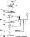
图1是一示意图,说明本发明汇流排系统的第一较佳实施例。FIG. 1 is a schematic diagram illustrating a first preferred embodiment of the busbar system of the present invention.
图2是一示意图,说明该第一较佳实施例的作动步骤。Fig. 2 is a schematic diagram illustrating the action steps of the first preferred embodiment.
图3是一示意图,明本发明汇流排系统的第二较佳实施例。FIG. 3 is a schematic diagram illustrating a second preferred embodiment of the busbar system of the present invention.
图4是一示意图,说明该第二较佳实施例的作动步骤。FIG. 4 is a schematic diagram illustrating the operation steps of the second preferred embodiment.
图5是一传输速率状态表。Fig. 5 is a transmission rate status table.
具体实施方式Detailed ways
有关本发明的前述及其他技术内容、特点与功效,在以下配合参考图式的二个较佳实施例的详细说明中,将可清楚的明白。而且,要先说明的是,在以下诸实施例中,相同的元件将以相同的标号标示。The aforementioned and other technical contents, features and effects of the present invention will be clearly understood in the following detailed description of two preferred embodiments with reference to the drawings. Moreover, it should be noted that in the following embodiments, the same components will be marked with the same reference numerals.
参阅图1,本发明自动调整传输速率的汇流排系统1的第一较佳实施例,包含一晶片组2及一汇流排模组3。Referring to FIG. 1 , the first preferred embodiment of the
晶片组2(chipset)是用以控制汇流排模组3及用以沟通汇流排模组3及一中央处理器(cpu)(图未示),在本较佳实施例中,此晶片组2为一北挢晶片组(North BridgeChipset),一般也称为系统控制晶片,其用以掌管电脑中的高速设备,由于此北挢晶片组为一市面上熟知且普偏使用的元件,在此不另行加以详细说明。Chipset 2 (chipset) is used to control the bus module 3 and to communicate with the bus module 3 and a central processing unit (cpu) (not shown). In this preferred embodiment, the chipset 2 It is a North Bridge Chipset (North Bridge Chipset), generally also called a system control chip, which is used to control high-speed devices in computers. Since the North Bridge Chipset is a well-known and commonly used component on the market, it will not be described here. Separately describe in detail.
汇流排模组3与该晶片组2耦接,并具有一汇流排31、复数汇流排插槽32、一缓冲器开关33、一开关控制器34及一转换器35,共同设置于一电脑主机板(图未示)上。其中,汇流排31耦接该晶片组2,即晶片组2设于该汇流排31的一控制端,于汇流排31上并依序供各汇流排插槽32(slot)耦接,每一汇流排插槽32可插设一符合该汇流排插槽32规格的介面卡(图未示),如网路卡、音效卡等,由汇流排31做为各介面卡与晶片组2讯号传输的通道。其中,在本较佳实施例中,因目前市面上主流的区域汇流排是为以PCI-X技术发展的PCI-X汇流排,所以在本实施例中的汇流排31,是指PCI-X汇流排,但是不应以此为限,此外,为说明方便,每一汇流排插槽32依其与晶片组2耦接顺序,可区分为第一汇流排插槽321、第二汇流排插槽322、第三汇流排插槽323,及第四汇流排插槽324,但是汇流排插槽32的插槽数目不应以此为限。The bus bar module 3 is coupled with the chipset 2, and has a
参阅图1,缓冲器开关33及开关控制器34共同界定一开关控制装置(图未示),缓冲器开关33(Buffer/Switch)耦接于该汇流排31上,由开关控制器34控制缓冲器开关33的启闭,其设置于该汇流排31上任意两汇流排插槽32间,在本较佳实施例中,只具有一缓冲器开关33,其是设置于第一及第二汇流排插槽321、322间,但是此汇流排系统1中,也可具有复数个缓冲器开关33,分别装设于任意两相邻汇流排插槽32间,此具有复数个缓冲器开关33的汇流排系统1的详细架构及技术,将于第二较佳实施例中再加以说明。1, the buffer switch 33 and the switch controller 34 jointly define a switch control device (not shown), the buffer switch 33 (Buffer/Switch) is coupled to the
开关控制器34用以控制缓冲器开关33的启闭,当电脑启动后,开关控制器34会先侦测第二汇流排插槽322是否插设有一介面卡(图未示),并依其侦测结果来决定是否再侦测第三汇流排插槽323,及第四汇流排插槽324,开关控制器34在侦测各汇流排插槽32时,可分别由所侦测的汇流排插槽32产生一二位元的使用状况识别码(prsnt1#,prsnt2#),而汇流排插槽322至324的使用状况识别码是依据各插设于上的介面卡所消耗功率的不同而有分别,若汇流排插槽322至324上并未插设有介面卡,则其所产生的使用状况识别码为(1,1),若其上插设有介面卡,则依据消耗功率的不同,分别产生有(0,1)、(1,0)、(0,0)等不同的使用状况识别码,值得注意的是,只要是有插设介面卡,其使用状况识别码(prsnt1#,prsnt2#)中,必有一者为0。The switch controller 34 is used to control the opening and closing of the buffer switch 33. When the computer is started, the switch controller 34 will first detect whether an interface card (not shown) is inserted into the second
当开关控制器34接收到各汇流排插槽322至324的使用状况识别码后,将对此等识别码进行一布林函数运算,并重置控制讯号C(示于图2)以控制缓冲器开关33的启闭。在本实施例中,此布林函数为一AND函数,所以除了当开关控制器34侦测汇流排插槽322至324所传回的使用状况识别码皆为(1,1),其控制讯号C经布林函数AND运算后方为1外,若汇流排插槽322至324中,任一插槽上插设有介面卡,此控制讯号C皆是为0。After the switch controller 34 receives the usage status identification codes of the
开关控制器34作完布林函数运算得到控制讯号C后,其传送控制讯号C至缓冲器开关33,当控制讯号C为0时,缓冲器开关33将启动,而使得第二、第三、第四汇流排插槽322、323、324与晶片组2保持通路,所以晶片组2在侦测汇流排插槽32数目时,将可测出目前此主机板上含有四个汇流排插槽32,因而控制汇流排31传输速度为66MHz。After the switch controller 34 completes the Bollinger function operation to obtain the control signal C, it transmits the control signal C to the buffer switch 33. When the control signal C is 0, the buffer switch 33 will be activated, so that the second, third, The fourth
相反地,若缓冲器开关33接收到控制讯号C为1时,其缓冲器开关33将关闭,而使得第二、第三、第四汇流排插槽322至324与晶片组2断路,所以晶片组2在侦测汇流排插槽32数目时,将测得目前此主机板上只含有一个汇流排插槽32,即第一汇流排插槽321,并因而控制汇流排31的传输速率为133MHz。如此一来,将可有效且自动视主机板上所插设使用的介面卡数量,来调整汇流排31传输速率,而不会受汇流排插槽32的数目而限制,值得说明的是,该开关控制器34所运算的布林函数也可为NAND,或以其它运算式来决定缓冲器开关33的启闭,并不因此而受限制,当然,若其运算法则改变,缓冲器开关33于接收控制讯号后所产生的动作,也需作相对修改,如若开关控制器34是以布林函数NAND作运算,则控制讯号C为0是用以控制缓冲器开关33关闭,1则是使缓冲器开关33启动。Conversely, if the buffer switch 33 receives the control signal C as 1, the buffer switch 33 will be closed, so that the second, third, and
此外,由于目前市面上相关于汇流排31所发展出较主流的技术除了PCI-X外,尚有一PCI Express技术,因此,为使以PCI Express为标准的晶片组2也可使用PCI-X汇流排31,所以本实施例中汇流排系统1将该转换器35设置于晶片组2及汇流排31间,用以将PCI Express与PCI-X讯号互做转换,使得此PCI-X汇流排31的使用,具有弹性。In addition, since there is a PCI Express technology besides PCI-X in the mainstream technology related to the
参阅图1、2,经上述就本发明的第一较佳实施例予以说明后,以下将就该较佳实施例对应的自动调整传输速率的方法的实施步骤,进一步详述。首先如步骤41,当使用者启动电脑后,如步骤42,开关控制器34会去侦测第二汇流排插槽322是否插设有介面卡,并对该汇流排插槽322产生一使用状况识别码prsnt1#,prsnt2#,开关控制器34并对此汇流排插槽322的使用状况识别码做一AND的布林函数运算,而产生一控制讯号C。如步骤43至44,当prsnt1#、prsnt2#中任一位元有一为0时,控制讯号C为0,此时,开关控制器34将控制缓冲器开关33启动,因此,第二至第四汇流排插槽322至324将与晶片组2通路,所以晶片组2在侦测汇流排插槽32的数目时,将可测出目前此主机板上含有四个汇流排插槽32,因而控制汇流排31传输速度为66MHz。如步骤45,当prsnt1#、prsnt2#皆为1时,控制讯号C为1,开关控制器34将侦测第三、第四汇流排插槽323、324是否插设有介面卡,如步骤46,并对汇流排插槽323、324的使用状况识别码prsnt1#、prsnt2#做一AND的布林函数运算,再重置控制讯号C,如步骤47,当控制讯号C为0时,缓冲器开关33启动,如步骤48,当控制讯号C为1时,代表第三、四连同前述第二汇流排插槽323、324、322上皆无插设介面卡,所以缓冲器开关33将关闭,而使得第二、第三,及第四汇流排插槽322、323、324皆与晶片组2断路,所以晶片组2在侦测汇流排插槽32的数目时,将测得目前此主机板上只含有一个汇流排插槽321,因而控制汇流排31的传输速率为133MHz。Referring to Figures 1 and 2, after the above description of the first preferred embodiment of the present invention, the implementation steps of the method for automatically adjusting the transmission rate corresponding to the preferred embodiment will be further described in detail below. First, as in
参阅图3,揭示的是本发明的第二较佳实施例,在以下的说明中,与第一较佳实施例类似的元件,是以相同的编号来表示,且由于使用技术大致相同,所以不再详细说明。但是其中值得注意的是,本第二较佳实施例中,具有一第一缓冲器开关331,及一第二缓冲器开关332,分别装设于第一汇流排插槽321与第二汇流排插槽322,及第二汇流排插槽322与第三汇流排插槽323间。此等缓冲器开关331、332也由开关控制器34来控制启闭,当第三、第四汇流排插槽323、324的使用状况识别码(prsnt1#,prsnt2#)经开关控制器34做一AND布林函数运算后,得一控制讯号C2,若C2为0,则第一、第二缓冲器开关331、332皆将启动,因此,第二至第四汇流排插槽322至324将与晶片组2通路,若C2为1,则开关控制器34对第二汇流排插槽322的控制讯号C1进行判读,若C1为0,则第一缓冲器开关331启动,第二缓冲器开关332关闭,所以第二汇流排插槽322将与晶片组2通路,而第三、第四汇流排插槽323、324将与晶片组2断路。晶片组2在侦测汇流排插槽32的数目时,将测得目前此主机板上只含有二个汇流排插槽321、322,因而控制汇流排31的传输速率为100MHz。若C1为1,则第一、第二缓冲器开关331、332皆关闭,所以第二、第三、第四汇流排插槽322、323、324将与晶片组2断路,晶片组2在侦测汇流排插槽32的数目时,将测得目前此主机板上只含有一个汇流排插槽321,因而控制汇流排31的传输速率为133MHz,其传输速率状态表请参阅图5。Referring to Fig. 3, it discloses the second preferred embodiment of the present invention. In the following description, elements similar to those of the first preferred embodiment are represented by the same numbers, and since the techniques used are substantially the same, No more details. However, it is worth noting that in this second preferred embodiment, there is a
参阅图3、4,以下将就本发明的第二较佳实施例的实施步骤,进一步详述。首先如步骤51当使用者启动电脑后,如步骤52,开关控制器34会去侦测第三、第四汇流排插槽323、324是否插设有介面卡,并对侦测汇流排插槽323、324,而产生的使用状况识别码prsnt1#,prsnt2#做一AND的布林函数运算,而产生一控制讯号C2。如步骤53当控制讯号C2为1,第一、第二缓冲器开关331、332将启动,因此,第二、第三、第四汇流排插槽322、323、324将与晶片组2通路,所以晶片组2在侦测汇流排插槽32的数目时,将可测出目前此主机板上含有四个汇流排插槽32,因而控制汇流排31传输速度为66MHz。Referring to Figures 3 and 4, the implementation steps of the second preferred embodiment of the present invention will be further described in detail below. First, as in
当控制讯号C2为0,此时,进入步骤54。同样地,开关控制器34会去侦测第二汇流排插槽322的使用状况,并对该汇流排插槽322的使用状况识别码做一AND的布林函数运算,并产生一控制讯号C1,如步骤55,当控制讯号C1为0时,第一缓冲器开关331启动,第二缓冲器开关332关闭,而使得第二汇流排插槽322与晶片组2通路,第三、第四汇流排插槽323、324与晶片组2断路。所以晶片组2在侦测汇流排插槽32的数目时,将测得主机板上含有二个汇流排插槽321、322,因而控制汇流排31的传输速率为100MHz,如步骤56,当控制讯号C1为1时,代表第二至第四汇流排插槽322至324上皆无插设介面卡,所以第一、第二缓冲器开关331、332将关闭,而使得第二至第四汇流排插槽322至324与晶片组2断路,所以晶片组2在侦测汇流排插槽32的数目时,将测得目前此主机板上只含有一个汇流排插槽321,因而控制汇流排31的传输速率为133MHz。When the control signal C2 is 0, at this time, go to step 54 . Similarly, the switch controller 34 will detect the usage status of the
Claims (20)
Priority Applications (1)
| Application Number | Priority Date | Filing Date | Title |
|---|---|---|---|
| CNB2004100461907ACN1297875C (en) | 2004-06-02 | 2004-06-02 | Bus system and method for automatically adjusting transmission rate |
Applications Claiming Priority (1)
| Application Number | Priority Date | Filing Date | Title |
|---|---|---|---|
| CNB2004100461907ACN1297875C (en) | 2004-06-02 | 2004-06-02 | Bus system and method for automatically adjusting transmission rate |
Publications (2)
| Publication Number | Publication Date |
|---|---|
| CN1704873A CN1704873A (en) | 2005-12-07 |
| CN1297875Ctrue CN1297875C (en) | 2007-01-31 |
Family
ID=35577149
Family Applications (1)
| Application Number | Title | Priority Date | Filing Date |
|---|---|---|---|
| CNB2004100461907AExpired - Fee RelatedCN1297875C (en) | 2004-06-02 | 2004-06-02 | Bus system and method for automatically adjusting transmission rate |
Country Status (1)
| Country | Link |
|---|---|
| CN (1) | CN1297875C (en) |
Citations (6)
| Publication number | Priority date | Publication date | Assignee | Title |
|---|---|---|---|---|
| US5887144A (en)* | 1996-11-20 | 1999-03-23 | International Business Machines Corp. | Method and system for increasing the load and expansion capabilities of a bus through the use of in-line switches |
| US5935233A (en)* | 1997-05-21 | 1999-08-10 | Micron Electronics, Inc. | Computer system with a switch interconnector for computer devices |
| US6182178B1 (en)* | 1998-06-30 | 2001-01-30 | International Business Machines Corporation | Method and system for supporting peripheral component interconnect (PCI) peer-to-peer access across a PCI host bridge supporting multiple PCI buses |
| US6269416B1 (en)* | 1999-02-02 | 2001-07-31 | Hewlett-Packard Company | Adaptive PCI slot |
| US6567882B1 (en)* | 1998-11-12 | 2003-05-20 | Nec Corporation | PCI function extension control device and method of PCI function extension control |
| CN1477480A (en)* | 2003-08-01 | 2004-02-25 | 威盛电子股份有限公司 | Plotting display structure and control chip group in it |
- 2004
- 2004-06-02CNCNB2004100461907Apatent/CN1297875C/ennot_activeExpired - Fee Related
Patent Citations (6)
| Publication number | Priority date | Publication date | Assignee | Title |
|---|---|---|---|---|
| US5887144A (en)* | 1996-11-20 | 1999-03-23 | International Business Machines Corp. | Method and system for increasing the load and expansion capabilities of a bus through the use of in-line switches |
| US5935233A (en)* | 1997-05-21 | 1999-08-10 | Micron Electronics, Inc. | Computer system with a switch interconnector for computer devices |
| US6182178B1 (en)* | 1998-06-30 | 2001-01-30 | International Business Machines Corporation | Method and system for supporting peripheral component interconnect (PCI) peer-to-peer access across a PCI host bridge supporting multiple PCI buses |
| US6567882B1 (en)* | 1998-11-12 | 2003-05-20 | Nec Corporation | PCI function extension control device and method of PCI function extension control |
| US6269416B1 (en)* | 1999-02-02 | 2001-07-31 | Hewlett-Packard Company | Adaptive PCI slot |
| CN1477480A (en)* | 2003-08-01 | 2004-02-25 | 威盛电子股份有限公司 | Plotting display structure and control chip group in it |
Also Published As
| Publication number | Publication date |
|---|---|
| CN1704873A (en) | 2005-12-07 |
Similar Documents
| Publication | Publication Date | Title |
|---|---|---|
| CN100377101C (en) | Method and system for testing mainboard containing fast peripheral component interconnection device | |
| US6041375A (en) | Method and system for enabling nondisruptive live insertion and removal of feature cards in a computer system | |
| US7447822B2 (en) | Hot-plug control system and method | |
| US20070073959A1 (en) | Dynamic reconfiguration of PCI express links | |
| US9645954B2 (en) | Embedded microcontroller and buses | |
| US7802043B2 (en) | Methods and apparatus for adding an autonomous controller to an existing architecture | |
| US8103993B2 (en) | Structure for dynamically allocating lanes to a plurality of PCI express connectors | |
| WO2019062218A1 (en) | Design method for implementing backplane lighting for multiple nvme hard disks | |
| GB2450591A (en) | USB port and plug that uses the PCI Express interface data transfer specification by having two pairs of data lines. | |
| US20070067541A1 (en) | Method and apparatus for automatically adjusting bus widths | |
| KR20010086335A (en) | Method of emulating an attachment and detachment of a usb device | |
| US20060168377A1 (en) | Reallocation of PCI express links using hot plug event | |
| WO2001025942A1 (en) | Method and apparatus for detecting the type of interface to which a peripheral device is connected | |
| CN105183679A (en) | Electronic device and information processing method | |
| CN114003528A (en) | OCP switching card, switching system and switching method | |
| CN116088648B (en) | Server cabinet, circuit control method and computing node | |
| US7124235B2 (en) | USB apparatus with switchable host/hub functions and control method thereof | |
| US20080049716A1 (en) | Error rate based power management of a high-speed serial link | |
| US20100058085A1 (en) | Power-Saving Device and Method | |
| CN1297875C (en) | Bus system and method for automatically adjusting transmission rate | |
| CN106502911A (en) | Multiple terminals access device | |
| CN100414526C (en) | Method and device for automatically adjusting bus width | |
| CN211349344U (en) | A motherboard and server | |
| CN107357744A (en) | It is a kind of to support HDD and the M.2 method and structure of storage medium self-identifying | |
| CN103034600A (en) | Electronic device with multiple data connection ports |
Legal Events
| Date | Code | Title | Description |
|---|---|---|---|
| C06 | Publication | ||
| PB01 | Publication | ||
| C10 | Entry into substantive examination | ||
| SE01 | Entry into force of request for substantive examination | ||
| C14 | Grant of patent or utility model | ||
| GR01 | Patent grant | ||
| CF01 | Termination of patent right due to non-payment of annual fee | Granted publication date:20070131 | |
| CF01 | Termination of patent right due to non-payment of annual fee |