CN1288715C - Silicon film crystallization method, thin film transistor using said method and its plate display - Google Patents
Silicon film crystallization method, thin film transistor using said method and its plate displayDownload PDFInfo
- Publication number
- CN1288715C CN1288715CCNB031580971ACN03158097ACN1288715CCN 1288715 CCN1288715 CCN 1288715CCN B031580971 ACNB031580971 ACN B031580971ACN 03158097 ACN03158097 ACN 03158097ACN 1288715 CCN1288715 CCN 1288715C
- Authority
- CN
- China
- Prior art keywords
- region
- thin film
- black matrix
- layer
- crystallization
- Prior art date
- Legal status (The legal status is an assumption and is not a legal conclusion. Google has not performed a legal analysis and makes no representation as to the accuracy of the status listed.)
- Expired - Lifetime
Links
Images


Classifications
- G—PHYSICS
- G02—OPTICS
- G02F—OPTICAL DEVICES OR ARRANGEMENTS FOR THE CONTROL OF LIGHT BY MODIFICATION OF THE OPTICAL PROPERTIES OF THE MEDIA OF THE ELEMENTS INVOLVED THEREIN; NON-LINEAR OPTICS; FREQUENCY-CHANGING OF LIGHT; OPTICAL LOGIC ELEMENTS; OPTICAL ANALOGUE/DIGITAL CONVERTERS
- G02F1/00—Devices or arrangements for the control of the intensity, colour, phase, polarisation or direction of light arriving from an independent light source, e.g. switching, gating or modulating; Non-linear optics
- G02F1/01—Devices or arrangements for the control of the intensity, colour, phase, polarisation or direction of light arriving from an independent light source, e.g. switching, gating or modulating; Non-linear optics for the control of the intensity, phase, polarisation or colour
- G02F1/13—Devices or arrangements for the control of the intensity, colour, phase, polarisation or direction of light arriving from an independent light source, e.g. switching, gating or modulating; Non-linear optics for the control of the intensity, phase, polarisation or colour based on liquid crystals, e.g. single liquid crystal display cells
- G02F1/133—Constructional arrangements; Operation of liquid crystal cells; Circuit arrangements
- G02F1/136—Liquid crystal cells structurally associated with a semi-conducting layer or substrate, e.g. cells forming part of an integrated circuit
- H—ELECTRICITY
- H01—ELECTRIC ELEMENTS
- H01L—SEMICONDUCTOR DEVICES NOT COVERED BY CLASS H10
- H01L21/00—Processes or apparatus adapted for the manufacture or treatment of semiconductor or solid state devices or of parts thereof
- H01L21/02—Manufacture or treatment of semiconductor devices or of parts thereof
- H01L21/02104—Forming layers
- H01L21/02365—Forming inorganic semiconducting materials on a substrate
- H01L21/02436—Intermediate layers between substrates and deposited layers
- H01L21/02494—Structure
- H01L21/02496—Layer structure
- H01L21/02502—Layer structure consisting of two layers
- C—CHEMISTRY; METALLURGY
- C30—CRYSTAL GROWTH
- C30B—SINGLE-CRYSTAL GROWTH; UNIDIRECTIONAL SOLIDIFICATION OF EUTECTIC MATERIAL OR UNIDIRECTIONAL DEMIXING OF EUTECTOID MATERIAL; REFINING BY ZONE-MELTING OF MATERIAL; PRODUCTION OF A HOMOGENEOUS POLYCRYSTALLINE MATERIAL WITH DEFINED STRUCTURE; SINGLE CRYSTALS OR HOMOGENEOUS POLYCRYSTALLINE MATERIAL WITH DEFINED STRUCTURE; AFTER-TREATMENT OF SINGLE CRYSTALS OR A HOMOGENEOUS POLYCRYSTALLINE MATERIAL WITH DEFINED STRUCTURE; APPARATUS THEREFOR
- C30B1/00—Single-crystal growth directly from the solid state
- C30B1/02—Single-crystal growth directly from the solid state by thermal treatment, e.g. strain annealing
- C30B1/023—Single-crystal growth directly from the solid state by thermal treatment, e.g. strain annealing from solids with amorphous structure
- C—CHEMISTRY; METALLURGY
- C30—CRYSTAL GROWTH
- C30B—SINGLE-CRYSTAL GROWTH; UNIDIRECTIONAL SOLIDIFICATION OF EUTECTIC MATERIAL OR UNIDIRECTIONAL DEMIXING OF EUTECTOID MATERIAL; REFINING BY ZONE-MELTING OF MATERIAL; PRODUCTION OF A HOMOGENEOUS POLYCRYSTALLINE MATERIAL WITH DEFINED STRUCTURE; SINGLE CRYSTALS OR HOMOGENEOUS POLYCRYSTALLINE MATERIAL WITH DEFINED STRUCTURE; AFTER-TREATMENT OF SINGLE CRYSTALS OR A HOMOGENEOUS POLYCRYSTALLINE MATERIAL WITH DEFINED STRUCTURE; APPARATUS THEREFOR
- C30B29/00—Single crystals or homogeneous polycrystalline material with defined structure characterised by the material or by their shape
- C30B29/02—Elements
- C30B29/06—Silicon
- G—PHYSICS
- G02—OPTICS
- G02F—OPTICAL DEVICES OR ARRANGEMENTS FOR THE CONTROL OF LIGHT BY MODIFICATION OF THE OPTICAL PROPERTIES OF THE MEDIA OF THE ELEMENTS INVOLVED THEREIN; NON-LINEAR OPTICS; FREQUENCY-CHANGING OF LIGHT; OPTICAL LOGIC ELEMENTS; OPTICAL ANALOGUE/DIGITAL CONVERTERS
- G02F1/00—Devices or arrangements for the control of the intensity, colour, phase, polarisation or direction of light arriving from an independent light source, e.g. switching, gating or modulating; Non-linear optics
- G02F1/01—Devices or arrangements for the control of the intensity, colour, phase, polarisation or direction of light arriving from an independent light source, e.g. switching, gating or modulating; Non-linear optics for the control of the intensity, phase, polarisation or colour
- G02F1/13—Devices or arrangements for the control of the intensity, colour, phase, polarisation or direction of light arriving from an independent light source, e.g. switching, gating or modulating; Non-linear optics for the control of the intensity, phase, polarisation or colour based on liquid crystals, e.g. single liquid crystal display cells
- G02F1/133—Constructional arrangements; Operation of liquid crystal cells; Circuit arrangements
- G02F1/136—Liquid crystal cells structurally associated with a semi-conducting layer or substrate, e.g. cells forming part of an integrated circuit
- G02F1/1362—Active matrix addressed cells
- G02F1/136209—Light shielding layers, e.g. black matrix, incorporated in the active matrix substrate, e.g. structurally associated with the switching element
- G—PHYSICS
- G02—OPTICS
- G02F—OPTICAL DEVICES OR ARRANGEMENTS FOR THE CONTROL OF LIGHT BY MODIFICATION OF THE OPTICAL PROPERTIES OF THE MEDIA OF THE ELEMENTS INVOLVED THEREIN; NON-LINEAR OPTICS; FREQUENCY-CHANGING OF LIGHT; OPTICAL LOGIC ELEMENTS; OPTICAL ANALOGUE/DIGITAL CONVERTERS
- G02F1/00—Devices or arrangements for the control of the intensity, colour, phase, polarisation or direction of light arriving from an independent light source, e.g. switching, gating or modulating; Non-linear optics
- G02F1/01—Devices or arrangements for the control of the intensity, colour, phase, polarisation or direction of light arriving from an independent light source, e.g. switching, gating or modulating; Non-linear optics for the control of the intensity, phase, polarisation or colour
- G02F1/13—Devices or arrangements for the control of the intensity, colour, phase, polarisation or direction of light arriving from an independent light source, e.g. switching, gating or modulating; Non-linear optics for the control of the intensity, phase, polarisation or colour based on liquid crystals, e.g. single liquid crystal display cells
- G02F1/133—Constructional arrangements; Operation of liquid crystal cells; Circuit arrangements
- G02F1/136—Liquid crystal cells structurally associated with a semi-conducting layer or substrate, e.g. cells forming part of an integrated circuit
- G02F1/1362—Active matrix addressed cells
- G02F1/1368—Active matrix addressed cells in which the switching element is a three-electrode device
- H—ELECTRICITY
- H01—ELECTRIC ELEMENTS
- H01L—SEMICONDUCTOR DEVICES NOT COVERED BY CLASS H10
- H01L21/00—Processes or apparatus adapted for the manufacture or treatment of semiconductor or solid state devices or of parts thereof
- H01L21/02—Manufacture or treatment of semiconductor devices or of parts thereof
- H01L21/02104—Forming layers
- H01L21/02365—Forming inorganic semiconducting materials on a substrate
- H01L21/02367—Substrates
- H01L21/0237—Materials
- H01L21/02422—Non-crystalline insulating materials, e.g. glass, polymers
- H—ELECTRICITY
- H01—ELECTRIC ELEMENTS
- H01L—SEMICONDUCTOR DEVICES NOT COVERED BY CLASS H10
- H01L21/00—Processes or apparatus adapted for the manufacture or treatment of semiconductor or solid state devices or of parts thereof
- H01L21/02—Manufacture or treatment of semiconductor devices or of parts thereof
- H01L21/02104—Forming layers
- H01L21/02365—Forming inorganic semiconducting materials on a substrate
- H01L21/02436—Intermediate layers between substrates and deposited layers
- H01L21/02439—Materials
- H01L21/02488—Insulating materials
- H—ELECTRICITY
- H01—ELECTRIC ELEMENTS
- H01L—SEMICONDUCTOR DEVICES NOT COVERED BY CLASS H10
- H01L21/00—Processes or apparatus adapted for the manufacture or treatment of semiconductor or solid state devices or of parts thereof
- H01L21/02—Manufacture or treatment of semiconductor devices or of parts thereof
- H01L21/02104—Forming layers
- H01L21/02365—Forming inorganic semiconducting materials on a substrate
- H01L21/02436—Intermediate layers between substrates and deposited layers
- H01L21/02439—Materials
- H01L21/02491—Conductive materials
- H—ELECTRICITY
- H01—ELECTRIC ELEMENTS
- H01L—SEMICONDUCTOR DEVICES NOT COVERED BY CLASS H10
- H01L21/00—Processes or apparatus adapted for the manufacture or treatment of semiconductor or solid state devices or of parts thereof
- H01L21/02—Manufacture or treatment of semiconductor devices or of parts thereof
- H01L21/02104—Forming layers
- H01L21/02365—Forming inorganic semiconducting materials on a substrate
- H01L21/02436—Intermediate layers between substrates and deposited layers
- H01L21/02494—Structure
- H01L21/02496—Layer structure
- H01L21/0251—Graded layers
- H—ELECTRICITY
- H01—ELECTRIC ELEMENTS
- H01L—SEMICONDUCTOR DEVICES NOT COVERED BY CLASS H10
- H01L21/00—Processes or apparatus adapted for the manufacture or treatment of semiconductor or solid state devices or of parts thereof
- H01L21/02—Manufacture or treatment of semiconductor devices or of parts thereof
- H01L21/02104—Forming layers
- H01L21/02365—Forming inorganic semiconducting materials on a substrate
- H01L21/02518—Deposited layers
- H01L21/02521—Materials
- H01L21/02524—Group 14 semiconducting materials
- H01L21/02532—Silicon, silicon germanium, germanium
- H—ELECTRICITY
- H01—ELECTRIC ELEMENTS
- H01L—SEMICONDUCTOR DEVICES NOT COVERED BY CLASS H10
- H01L21/00—Processes or apparatus adapted for the manufacture or treatment of semiconductor or solid state devices or of parts thereof
- H01L21/02—Manufacture or treatment of semiconductor devices or of parts thereof
- H01L21/02104—Forming layers
- H01L21/02365—Forming inorganic semiconducting materials on a substrate
- H01L21/02656—Special treatments
- H01L21/02664—Aftertreatments
- H01L21/02667—Crystallisation or recrystallisation of non-monocrystalline semiconductor materials, e.g. regrowth
- H01L21/02672—Crystallisation or recrystallisation of non-monocrystalline semiconductor materials, e.g. regrowth using crystallisation enhancing elements
- H—ELECTRICITY
- H10—SEMICONDUCTOR DEVICES; ELECTRIC SOLID-STATE DEVICES NOT OTHERWISE PROVIDED FOR
- H10D—INORGANIC ELECTRIC SEMICONDUCTOR DEVICES
- H10D30/00—Field-effect transistors [FET]
- H10D30/01—Manufacture or treatment
- H10D30/021—Manufacture or treatment of FETs having insulated gates [IGFET]
- H10D30/031—Manufacture or treatment of FETs having insulated gates [IGFET] of thin-film transistors [TFT]
- H10D30/0312—Manufacture or treatment of FETs having insulated gates [IGFET] of thin-film transistors [TFT] characterised by the gate electrodes
- H10D30/0314—Manufacture or treatment of FETs having insulated gates [IGFET] of thin-film transistors [TFT] characterised by the gate electrodes of lateral top-gate TFTs comprising only a single gate
- H—ELECTRICITY
- H10—SEMICONDUCTOR DEVICES; ELECTRIC SOLID-STATE DEVICES NOT OTHERWISE PROVIDED FOR
- H10D—INORGANIC ELECTRIC SEMICONDUCTOR DEVICES
- H10D30/00—Field-effect transistors [FET]
- H10D30/01—Manufacture or treatment
- H10D30/021—Manufacture or treatment of FETs having insulated gates [IGFET]
- H10D30/031—Manufacture or treatment of FETs having insulated gates [IGFET] of thin-film transistors [TFT]
- H10D30/0321—Manufacture or treatment of FETs having insulated gates [IGFET] of thin-film transistors [TFT] comprising silicon, e.g. amorphous silicon or polysilicon
- H—ELECTRICITY
- H10—SEMICONDUCTOR DEVICES; ELECTRIC SOLID-STATE DEVICES NOT OTHERWISE PROVIDED FOR
- H10D—INORGANIC ELECTRIC SEMICONDUCTOR DEVICES
- H10D30/00—Field-effect transistors [FET]
- H10D30/60—Insulated-gate field-effect transistors [IGFET]
- H10D30/67—Thin-film transistors [TFT]
- H10D30/6729—Thin-film transistors [TFT] characterised by the electrodes
- H10D30/673—Thin-film transistors [TFT] characterised by the electrodes characterised by the shapes, relative sizes or dispositions of the gate electrodes
- H10D30/6731—Top-gate only TFTs
- H—ELECTRICITY
- H10—SEMICONDUCTOR DEVICES; ELECTRIC SOLID-STATE DEVICES NOT OTHERWISE PROVIDED FOR
- H10D—INORGANIC ELECTRIC SEMICONDUCTOR DEVICES
- H10D30/00—Field-effect transistors [FET]
- H10D30/60—Insulated-gate field-effect transistors [IGFET]
- H10D30/67—Thin-film transistors [TFT]
- H10D30/674—Thin-film transistors [TFT] characterised by the active materials
- H10D30/6741—Group IV materials, e.g. germanium or silicon carbide
- H10D30/6743—Silicon
- H10D30/6745—Polycrystalline or microcrystalline silicon
- H—ELECTRICITY
- H10—SEMICONDUCTOR DEVICES; ELECTRIC SOLID-STATE DEVICES NOT OTHERWISE PROVIDED FOR
- H10D—INORGANIC ELECTRIC SEMICONDUCTOR DEVICES
- H10D86/00—Integrated devices formed in or on insulating or conducting substrates, e.g. formed in silicon-on-insulator [SOI] substrates or on stainless steel or glass substrates
- H10D86/01—Manufacture or treatment
- H10D86/021—Manufacture or treatment of multiple TFTs
- H10D86/0221—Manufacture or treatment of multiple TFTs comprising manufacture, treatment or patterning of TFT semiconductor bodies
- H10D86/0223—Manufacture or treatment of multiple TFTs comprising manufacture, treatment or patterning of TFT semiconductor bodies comprising crystallisation of amorphous, microcrystalline or polycrystalline semiconductor materials
- H10D86/0227—Manufacture or treatment of multiple TFTs comprising manufacture, treatment or patterning of TFT semiconductor bodies comprising crystallisation of amorphous, microcrystalline or polycrystalline semiconductor materials using structural arrangements to control crystal growth, e.g. placement of grain filters
- G—PHYSICS
- G02—OPTICS
- G02F—OPTICAL DEVICES OR ARRANGEMENTS FOR THE CONTROL OF LIGHT BY MODIFICATION OF THE OPTICAL PROPERTIES OF THE MEDIA OF THE ELEMENTS INVOLVED THEREIN; NON-LINEAR OPTICS; FREQUENCY-CHANGING OF LIGHT; OPTICAL LOGIC ELEMENTS; OPTICAL ANALOGUE/DIGITAL CONVERTERS
- G02F2202/00—Materials and properties
- G02F2202/10—Materials and properties semiconductor
- G02F2202/105—Materials and properties semiconductor single crystal Si
- H—ELECTRICITY
- H10—SEMICONDUCTOR DEVICES; ELECTRIC SOLID-STATE DEVICES NOT OTHERWISE PROVIDED FOR
- H10K—ORGANIC ELECTRIC SOLID-STATE DEVICES
- H10K59/00—Integrated devices, or assemblies of multiple devices, comprising at least one organic light-emitting element covered by group H10K50/00
- H10K59/10—OLED displays
- H10K59/12—Active-matrix OLED [AMOLED] displays
Landscapes
- Engineering & Computer Science (AREA)
- Physics & Mathematics (AREA)
- Microelectronics & Electronic Packaging (AREA)
- Chemical & Material Sciences (AREA)
- General Physics & Mathematics (AREA)
- Condensed Matter Physics & Semiconductors (AREA)
- Power Engineering (AREA)
- Computer Hardware Design (AREA)
- Manufacturing & Machinery (AREA)
- Crystallography & Structural Chemistry (AREA)
- Nonlinear Science (AREA)
- Materials Engineering (AREA)
- Optics & Photonics (AREA)
- Mathematical Physics (AREA)
- Metallurgy (AREA)
- Organic Chemistry (AREA)
- Thermal Sciences (AREA)
- Thin Film Transistor (AREA)
- Recrystallisation Techniques (AREA)
- Liquid Crystal (AREA)
Abstract
Translated fromChinese
Description
Translated fromChinese相关申请的交叉引用Cross References to Related Applications
本申请要求2002年8月3日在韩国知识产权局申请的韩国专利申请号为No.2002-45955的优先权,其公开的技术方案在此作引用参考。This application claims the priority of Korean Patent Application No. 2002-45955 filed at the Korean Intellectual Property Office on August 3, 2002, and its disclosed technical solutions are hereby cited for reference.
1.技术领域1. Technical field
本发明涉及一种非晶硅薄膜的结晶方法,更具体地说,涉及一种使用该结晶方法形成薄膜晶体管(TFT)的方法,该薄膜晶体管应用于如液晶显示器(LCD)、发光显示器(LED)和三维超大规模集成(VLSI)半导体器件等的平板显示器中,一种使用该方法制造的TFT,和一种包括该TFT的平板显示器。The present invention relates to a kind of crystallization method of amorphous silicon thin film, relate to a kind of method using this crystallization method to form thin-film transistor (TFT) more particularly, and this thin-film transistor is applied to such as liquid crystal display (LCD), light-emitting display (LED) ), and a flat panel display of a three-dimensional very large scale integration (VLSI) semiconductor device, etc., a TFT manufactured using the method, and a flat panel display including the TFT.
2.背景技术2. Background technology
通常,在如液晶显示器(LCD)、有机或无机发光显示器(OLED或LED)等平板显示器中使用的非晶硅薄膜晶体管(a-Si TFT)将非晶硅用于包括一源极、一漏极和一沟道的半导体有源层,并提供1cm2/Vs或更小的低电子迁移率。因此,这样的a-Si TFT最近已被多晶硅TFT(poly-Si TFT)代替。多晶硅TFT提供的电子迁移率比a-Si TFT要大,可对光辐射稳定。因此,多晶硅TFT能够用作有源矩阵LCD或有源矩阵有机LED的驱动和/或开关晶体管。Generally, amorphous silicon thin film transistors (a-Si TFTs) used in flat panel displays such as liquid crystal displays (LCDs), organic or inorganic light-emitting displays (OLEDs or LEDs) use amorphous silicon for electrode and a channel semiconductor active layer, and provide a low electron mobility of 1 cm2 /Vs or less. Therefore, such a-Si TFTs have recently been replaced by polysilicon TFTs (poly-Si TFTs). Polysilicon TFTs provide greater electron mobility than a-Si TFTs and are stable against light radiation. Thus, polysilicon TFTs can be used as driving and/or switching transistors for active matrix LCDs or active matrix organic LEDs.
典型的是,通过直接沉积多晶硅或通过在非晶硅沉积后对其进行结晶来制造多晶硅TFT。Typically, polysilicon TFTs are fabricated by directly depositing polysilicon or by crystallizing amorphous silicon after it has been deposited.
直接沉积多晶硅的方法的实例包括化学气相沉积(CVD)、光CVD、氢根(HR)CVD、电子回旋共振(ECR)CVD、等离子增强型(PE)CVD和低压(LP)CVD。Examples of methods of directly depositing polysilicon include chemical vapor deposition (CVD), photo CVD, hydrogen radical (HR) CVD, electron cyclotron resonance (ECR) CVD, plasma enhanced (PE) CVD, and low pressure (LP) CVD.
在沉积后对非晶硅进行结晶的方法的实例包括一固相结晶(SPC)、一准分子激光器结晶(ELC)、一连续横向固化(SLS)、一金属诱导结晶(MIC)和一金属诱导横向结晶(MILC)。Examples of methods for crystallizing amorphous silicon after deposition include a solid-phase crystallization (SPC), an excimer laser crystallization (ELC), a sequential lateral solidification (SLS), a metal-induced crystallization (MIC), and a metal-induced Lateral Crystallization (MILC).
但是,使用SPC是不切实际的,因为它需要一个较长的在600℃或更高的高温过程的持续时间。虽然ELC具有低温结晶的优点,但是通过光学系统发散的用于结晶的激光束的强度均匀性是较差的。另一方面,SLS涉及通过一人字图案掩模将一激光束照射到一非晶硅层上以形成一结晶的多晶硅的局部区域并需要对激光照射进行精确的控制。而且,使用SLS再现具有均匀特性的这种多晶硅薄膜是比较困难的。MIC具有低温结晶的优点,因为用作结晶催化剂的金属薄膜在非晶硅层结晶之前先沉积在非晶硅层的表面上。但是,由MIC形成的多晶硅层包含较小无序的晶体,残留在多晶硅层中的金属降低了由其制成的薄膜晶体管的性能。However, using SPC is impractical because it requires a longer duration of high temperature process at 600°C or higher. Although ELC has the advantage of low-temperature crystallization, the intensity uniformity of a laser beam for crystallization diverged through an optical system is poor. On the other hand, SLS involves irradiating a laser beam onto an amorphous silicon layer through a chevron pattern mask to form a localized region of crystalline polysilicon and requires precise control of the laser irradiation. Furthermore, it is relatively difficult to reproduce such polysilicon thin films with uniform characteristics using SLS. MIC has the advantage of low-temperature crystallization because a metal thin film used as a crystallization catalyst is deposited on the surface of the amorphous silicon layer before crystallization of the amorphous silicon layer. However, the polysilicon layer formed by MIC contains smaller disordered crystals, and the metal remaining in the polysilicon layer degrades the performance of thin film transistors made from it.
最近,MILC已被建议用作一种解决由上述常用非晶硅结晶方法引起的问题的方案。MILC通过用金属与硅起反应以形成硅化物来诱导横向的连续结晶。在MILC中,用于非晶硅层结晶的金属几乎不会残留在半导体有源层中,形成的晶体具有晶粒小和高度有序的特点。因此,不会产生由于残留金属组分而形成的电流泄漏和其它电性能的降低。而且,通过MILC的结晶可在相对较低的温度300-500℃进行诱导。Recently, MILC has been suggested as a solution to the problems caused by the above-mentioned conventional amorphous silicon crystallization methods. MILCs induce lateral continuous crystallization by reacting metal with silicon to form silicides. In MILC, the metal used for the crystallization of the amorphous silicon layer hardly remains in the semiconductor active layer, and the formed crystals are characterized by small crystal grains and high order. Therefore, current leakage and other reductions in electrical properties due to residual metal components do not occur. Moreover, crystallization by MILC can be induced at relatively low temperatures of 300-500 °C.
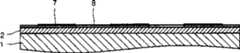
图1A至1D表示一种使用这种常用的MILC方法形成多晶硅层的方法。1A to 1D show a method of forming a polysilicon layer using this conventional MILC method.
参考图1A,在一透明衬底1上使用SiOx形成一缓冲层2,将一非晶硅层3沉积在缓冲层2上。将一绝缘层4沉积在非晶硅层3上,并形成如具有一预定图案的光致抗蚀剂层的一感光层5。然后,如图1B所示,通过使用感光层5将非晶硅层3上的绝缘层4蚀刻成一预定图案,一镍(Ni)薄膜6沉积在其上面作为结晶的催化剂。此后,进行热处理。其结果,如图1C所示,作为金属诱导结晶的结果,在从中去除了绝缘层4的非晶硅层3的区域A中形成一MIC区7,作为MIC区7横向结晶的结果,在区域B中形成一MILC层8,在区域B中绝缘层4未进行蚀刻。下面,如图1D所示,绝缘层4从MILC区8中去除以提供一多晶硅薄膜。Referring to FIG. 1A , a buffer layer 2 is formed using SiOx on a
在一非晶硅薄膜上形成一栅极介电层和一栅电极后,在使用这样的MILC形成一TFT之处,在其上形成一Ni薄膜,并对其进行热处理以便结晶。另一种可选择的方案是,在形成一栅极介电层和一栅电极后,涂敷一光致抗蚀剂覆盖栅极介电层、栅电极,并部分覆盖一源极区和一漏极区,并将一Ni薄膜形成在其上面。然后,为了通过热处理结晶去除光致抗蚀剂。在上述情况下,所产生的具有不同结晶结构的MIC和MILC区域的边界与源极/沟道边界和漏极/沟道边界不对准。因此,就会降低沟道区域的特性。After forming a gate dielectric layer and a gate electrode on an amorphous silicon film, where such a MILC is used to form a TFT, a Ni film is formed thereon and subjected to heat treatment for crystallization. Another alternative is to apply a photoresist to cover the gate dielectric layer, the gate electrode, and partially cover a source region and a gate electrode after forming a gate dielectric layer and a gate electrode. drain region, and a Ni film is formed thereon. Then, the photoresist is removed for crystallization by heat treatment. In the above cases, the boundaries of the resulting MIC and MILC regions with different crystalline structures are misaligned with the source/channel boundaries and drain/channel boundaries. Therefore, the characteristics of the channel region are degraded.
而且,如上所述,常用的MILC需要冗长的操作过程,该操作过程包括用于较大MILC区域的光致抗蚀剂层形成和一结晶催化剂沉积,因此制造TFT就比较复杂。Also, as described above, conventional MILCs require lengthy operations including photoresist layer formation and deposition of a crystallization catalyst for a larger MILC area, and thus the fabrication of TFTs is complicated.
发明内容Contents of the invention
因此,本发明的一个方面是提供一种通过使用黑色基质(black matrix)的非晶硅薄膜的结晶方法,与常用的结晶方法相比,该方法简单。Accordingly, an aspect of the present invention is to provide a crystallization method of an amorphous silicon thin film by using a black matrix, which is simple compared with conventional crystallization methods.
本发明的另一个方面是提供一种具有改善性能的薄膜晶体管(TFT),其中形成的一金属诱导的结晶(MIC)区域和一金属诱导横向结晶(MILC)区域是连续的而没有明确限定的边界。Another aspect of the present invention is to provide a thin film transistor (TFT) with improved performance, wherein a metal-induced crystallization (MIC) region and a metal-induced lateral crystallization (MILC) region are formed continuously without being clearly defined boundary.
本发明的又一个方面是提供一种非晶硅薄层的结晶方法,该方法通过使用一同时发生的黑色基质层形成和结晶,与常用的结晶方法相比,它包括较少的处理操作。Still another aspect of the present invention is to provide a method of crystallizing a thin layer of amorphous silicon by using a simultaneous black matrix layer formation and crystallization which involves fewer processing operations than conventional crystallization methods.
本发明的其它目的和/或优点将在下面的描述部分中被提及,从该描述中,部分目的和/或优点将会显而易见,或者可从本发明的实践中获知。Other purposes and/or advantages of the present invention will be mentioned in the following description, and part of the purposes and/or advantages will be apparent from the description, or can be learned from the practice of the present invention.
为了实现本发明的上述和/或其它目的,提供一种非晶硅薄膜的结晶方法,该方法包括在衬底上形成一黑色基质层以吸收外部光,该黑色基质层的上部区域具有用于结晶的催化剂,构图该黑色基质层,在衬底和该黑色基质层上形成非晶硅薄膜,对非晶硅薄膜进行热处理用于结晶。In order to achieve the above and/or other purposes of the present invention, a method for crystallizing an amorphous silicon thin film is provided, the method comprising forming a black matrix layer on a substrate to absorb external light, the upper region of the black matrix layer has a A crystallized catalyst, patterning the black matrix layer, forming an amorphous silicon film on the substrate and the black matrix layer, heat-treating the amorphous silicon film for crystallization.
黑色基质层的形成可包括:形成一功能薄膜,该薄膜具有在其面对衬底的下部区域中的透明第一组分和在其上部区域中的金属第二组分。该功能薄膜的形成可包括形成随着到绝缘衬底距离的增加浓度逐渐下降的透明第一组分和浓度逐渐提高的金属第二组分。The forming of the black matrix layer may include forming a functional thin film having a transparent first component in a lower region thereof facing the substrate and a metallic second component in an upper region thereof. The formation of the functional thin film may include forming a transparent first component whose concentration gradually decreases with increasing distance from the insulating substrate and a metal second component whose concentration gradually increases.
透明第一组分可包括从下面的组中选择的至少一个,由SiOx,这里x≥1、SiNx,这里x≥1、MgF2、CaF2、Al2O3和SnO2组成的组,这些是透明绝缘材料,由ITO、IZO、ZnO和In2O3组成的组,这些是透明导电材料。金属第二组分可包括从下面的组中选择的至少一种金属,该组包括:Fe、Co、V、Ti、Al、Ag、Si、Ge、Y、Zn、Zr、W、Ta、Cu、和Pt。The transparent first component may comprise at least one selected from the group consisting ofSiOx , where x≥1,SiNx , where x≥1,MgF2 ,CaF2 ,Al2O3, andSnO2 , these are transparent insulating materials, the group consisting of ITO, IZO, ZnO andIn2O3 , these are transparent conductive materials. The metal second component may comprise at least one metal selected from the group consisting of: Fe, Co, V, Ti, Al, Ag, Si, Ge, Y, Zn, Zr, W, Ta, Cu , and Pt.
黑色基质的形成可包括:在衬底上形成具有第一CrOx薄膜的功能薄膜,这里x≥1;和在第一薄膜上形成一由Cr制成的第二薄膜。The formation of the black matrix may include: forming a functional film having a firstCrOx film on the substrate, where x≥1; and forming a second film made of Cr on the first film.
黑色基质层可包括一CrOx薄膜,这里x≥1,或一Cr薄膜。The black matrix layer may include aCrOx film, where x≥1, or a Cr film.
黑色基质层可用于一平板显示器,黑色基质层的构图可包括与一能暴露平板显示器的像素区的构图操作同时实现的构图黑色基质层。The black matrix layer may be used in a flat panel display, and patterning of the black matrix layer may include patterning the black matrix layer simultaneously with a patterning operation that exposes pixel regions of the flat panel display.
硅结晶的催化剂可包括从下面的组中选择的至少一种,该组包括:Ni、Pd、Au、Sn、Sb、Cr、Mo、Tr、Ru、Rh、Fe、Co、V、Ti、Al、Ag、Cu和Pt。The catalyst for silicon crystallization may include at least one selected from the group consisting of: Ni, Pd, Au, Sn, Sb, Cr, Mo, Tr, Ru, Rh, Fe, Co, V, Ti, Al , Ag, Cu and Pt.
为了实现本发明的上述和/或其它目的,提供非晶硅薄膜的另一种结晶方法,该方法包括在衬底上形成一黑色基质层以吸收外部光;在该黑色基质层上形成具有用于结晶的催化剂的结晶薄膜;构图该黑色基质层和结晶薄膜;在绝缘衬底和构图过的结晶薄膜上形成非晶硅薄膜;对非晶硅薄膜进行热处理以用于结晶。In order to achieve the above and/or other purposes of the present invention, another crystallization method of an amorphous silicon thin film is provided, the method comprising forming a black matrix layer on a substrate to absorb external light; A crystalline thin film of a crystallized catalyst; patterning the black matrix layer and the crystalline thin film; forming an amorphous silicon thin film on an insulating substrate and the patterned crystalline thin film; and heat-treating the amorphous silicon thin film for crystallization.
黑色基质层的形成可包括:形成一功能薄膜,该功能薄膜具有在其面对衬底的下部区域中的透明第一组分和在其上部区域中的金属第二组分。该功能薄膜的形成可包括形成随着到衬底距离的增加浓度逐渐下降的透明第一组分和浓度逐渐提高的金属第二组分。The forming of the black matrix layer may include forming a functional thin film having a transparent first component in a lower region thereof facing the substrate and a metallic second component in an upper region thereof. Forming the functional thin film may include forming a transparent first component whose concentration gradually decreases with increasing distance from the substrate and a metal second component whose concentration gradually increases.
透明第一组分可包括从下面的组中选择的至少一个,由SiOx,这里x≥1、SiNx,这里x≥1、MgF2、CaF2、Al2O3和SnO2组成的组,这些是透明绝缘材料,由ITO、IZO、ZnO和In2O3组成的组,这些都是透明导电材料。金属第二组分可包括从下面的组中选择的至少一种金属,该组包括:Fe、Co、V、Ti、Al、Ag、Si、Ge、Y、Zn、Zr、W、Ta、Cu、和Pt。The transparent first component may comprise at least one selected from the group consisting ofSiOx , where x≥1,SiNx , where x≥1,MgF2 ,CaF2 ,Al2O3, andSnO2 , these are transparent insulating materials,a group consisting of ITO, IZO, ZnO andIn2O3 , these are transparent conductive materials. The metal second component may comprise at least one metal selected from the group consisting of: Fe, Co, V, Ti, Al, Ag, Si, Ge, Y, Zn, Zr, W, Ta, Cu , and Pt.
黑色基质层可包括一CrOx薄膜,这里x≥1,或一Cr薄膜。The black matrix layer may include aCrOx film, where x≥1, or a Cr film.
黑色基质层可为一功能薄膜,它具有在绝缘衬底上由CrOx形成的第一薄膜,这里x≥1;和在第一薄膜上一由Cr形成的第二薄膜。The black matrix layer may be a functional film having a first film formed ofCrOx , where x≥1, on an insulating substrate; and a second film formed of Cr on the first film.
黑色基质层可用于一平板显示器,黑色基质层的构图可包括与一暴露平板显示器的像素区的构图操作同时实现的构图黑色基质层。The black matrix layer can be used in a flat panel display, and patterning of the black matrix layer can include patterning the black matrix layer simultaneously with a patterning operation exposing pixel regions of the flat panel display.
硅结晶的催化剂可包括从下面的组中选择的至少一种,该组包括:Ni、Pd、Au、Sn、Sb、Cr、Mo、Tr、Ru、Rh、Fe、Co、V、Ti、Al、Ag、Cu和Pt。The catalyst for silicon crystallization may include at least one selected from the group consisting of: Ni, Pd, Au, Sn, Sb, Cr, Mo, Tr, Ru, Rh, Fe, Co, V, Ti, Al , Ag, Cu and Pt.
为了实现本发明的上述和/或其它目的,提供一种薄膜晶体管,它包括一衬底和一在衬底上形成的具有沟道区、源极区和漏极区的半导体有源层,其中源极区和漏极区在沟道区的相应侧形成,至少是沟道区形成为一金属诱导横向结晶(MILC)区。该薄膜晶体管还包括一置于衬底和至少半导体有源层的源极区和漏极区之间的黑色基质层,其中该黑色基质层的上部区域包括一结晶用的催化剂,一在沟道区上形成的栅极介电层和一在栅极介电层上形成的栅电极。In order to achieve the above and/or other purposes of the present invention, a thin film transistor is provided, which includes a substrate and a semiconductor active layer formed on the substrate with a channel region, a source region and a drain region, wherein Source and drain regions are formed on respective sides of the channel region, at least the channel region is formed as a metal induced lateral crystallization (MILC) region. The thin film transistor also includes a black matrix layer placed between the substrate and at least the source region and the drain region of the semiconductor active layer, wherein the upper region of the black matrix layer includes a catalyst for crystallization, and a A gate dielectric layer is formed on the region and a gate electrode is formed on the gate dielectric layer.
通过使用高浓度的杂质离子的掺杂方法可形成源极区和漏极区。The source region and the drain region may be formed by a doping method using a high concentration of impurity ions.
该黑色基质层可从源极区和漏极区往下向沟道区倾斜。The black matrix layer may slope downward from the source and drain regions to the channel region.
源极区和漏极区中的每个可包括一面对沟道区的结合区和一金属诱导结晶(MIC)区,该结合区可包括一部分MILC区和一部分MIC区。Each of the source region and the drain region may include a junction region facing the channel region and a metal induced crystallization (MIC) region, and the junction region may include a portion of the MILC region and a portion of the MIC region.
该薄膜晶体管还包括一硅结晶催化剂薄膜,该薄膜包括从下面的组中选择的至少一种金属,该组包括:Ni、Pd、Au、Sn、Sb、Cr、Mo、Tr、Ru、Rh、Fe、Co、V、Ti、Al、Ag、Cu和Pt,该薄膜设置在黑色基质层和源极区和漏极区之间。The thin film transistor also includes a silicon crystallization catalyst film including at least one metal selected from the group consisting of: Ni, Pd, Au, Sn, Sb, Cr, Mo, Tr, Ru, Rh, Fe, Co, V, Ti, Al, Ag, Cu and Pt, the thin film is arranged between the black matrix layer and the source and drain regions.
为了实现本发明的上述和/或其它目的,提供一种平板显示器,它包括一绝缘衬底;一像素区,该像素区包括在绝缘衬底上排列成一矩阵的像素;和至少一个靠近像素区的薄膜晶体管。该至少一个薄膜晶体管包括一在绝缘衬底上形成的具有沟道区、源极区和漏极区的半导体有源层,源极区和漏极区在沟道区的相应侧形成,其中至少是沟道区形成为一金属诱导横向结晶(MILC)区;形成在沟道区上的一栅极介电层,形成在栅极介电层上的一栅电极,和置于绝缘衬底和栅极介电层之间的一黑色基质层,黑色基质层具有一至少暴露半导体有源层的源极区和漏极区之间沟道区的开口和一暴露像素区的开口。In order to realize the above-mentioned and/or other objects of the present invention, a kind of flat panel display is provided, and it comprises an insulating substrate; A pixel area, this pixel area comprises the pixel that is arranged in a matrix on the insulating substrate; And at least one near pixel area thin film transistors. The at least one thin film transistor comprises a semiconductor active layer formed on an insulating substrate with a channel region, a source region and a drain region, the source region and the drain region are formed on respective sides of the channel region, wherein at least The channel region is formed as a metal-induced lateral crystallization (MILC) region; a gate dielectric layer is formed on the channel region, a gate electrode is formed on the gate dielectric layer, and an insulating substrate and A black matrix layer between the gate dielectric layers, the black matrix layer has an opening exposing at least the channel region between the source region and the drain region of the semiconductor active layer and an opening exposing the pixel region.
该薄膜晶体管还包括一在栅电极和栅极介电层上形成的层间绝缘层;在层间绝缘层上形成并分别与半导体有源层的源极区和漏极区电连接的源电极和漏电极;和一在层间绝缘层、源电极和漏电极上形成能将像素区的像素电极与漏电极相连接的钝化层。The thin film transistor also includes an interlayer insulating layer formed on the gate electrode and the gate dielectric layer; a source electrode formed on the interlayer insulating layer and electrically connected to the source region and the drain region of the semiconductor active layer respectively and a drain electrode; and a passivation layer that can connect the pixel electrode and the drain electrode in the pixel area is formed on the interlayer insulating layer, the source electrode and the drain electrode.
通过使用高浓度的杂质离子的掺杂方法可形成源极区和漏极区。The source region and the drain region may be formed by a doping method using a high concentration of impurity ions.
该黑色基质层从源极区和漏极区往下向沟道区倾斜。The black matrix layer slopes downward from the source and drain regions to the channel region.
源极区和漏极区中的每个可包括一面对沟道区的结合区和一金属诱导结晶(MIC)区,该结合区可包括一部分MILC区和一部分MIC区。Each of the source region and the drain region may include a junction region facing the channel region and a metal induced crystallization (MIC) region, and the junction region may include a portion of the MILC region and a portion of the MIC region.
面对半导体有源层的黑色基质层的上部区域包括从下面的组中选择的至少一种金属,该组包括:Ni、Pd、Au、Sn、Sb、Cr、Mo、Tr、Ru、Rh、Fe、Co、V、Ti、Al、Ag、Cu和Pt。The upper region of the black matrix layer facing the semiconductor active layer includes at least one metal selected from the group consisting of: Ni, Pd, Au, Sn, Sb, Cr, Mo, Tr, Ru, Rh, Fe, Co, V, Ti, Al, Ag, Cu and Pt.
平板显示器还可包括一硅结晶催化剂薄膜,它包括从下面的组中选择的至少一种,该组包括:Ni、Pd、Au、Sn、Sb、Cr、Mo、Tr、Ru、Rh、Fe、Co、V、Ti、Al、Ag、Cu和Pt,该薄膜设置在黑色基质层和半导体有源层的源极区和漏极区之间。The flat panel display may also include a silicon crystallization catalyst film comprising at least one selected from the group consisting of: Ni, Pd, Au, Sn, Sb, Cr, Mo, Tr, Ru, Rh, Fe, Co, V, Ti, Al, Ag, Cu and Pt, the thin film is arranged between the black matrix layer and the source region and the drain region of the semiconductor active layer.
附图说明Description of drawings
本发明的这些和/或其它目的和效果从下面结合附图的优选实施例的描述中将会变得比较明显和更易于理解。These and/or other objects and effects of the present invention will become more apparent and easier to understand from the following description of preferred embodiments in conjunction with the accompanying drawings.
图1A至1D是表示通过使用一种常用金属诱导横向结晶方法形成一多晶硅层的方法的视图;1A to 1D are views showing a method of forming a polysilicon layer by using a conventional metal-induced lateral crystallization method;
图2至4是表示根据本发明一个实施例的非晶硅薄膜的结晶方法的剖视图;2 to 4 are cross-sectional views showing a crystallization method of an amorphous silicon thin film according to an embodiment of the present invention;
图5是图3的区域III的放大剖视图;Fig. 5 is an enlarged sectional view of area III of Fig. 3;
图6是图4的区域IV的放大剖视图;FIG. 6 is an enlarged cross-sectional view of area IV of FIG. 4;
图7是图2的功能薄膜的浓度梯度曲线图;Fig. 7 is the concentration gradient curve diagram of the functional thin film of Fig. 2;
图8是图2的功能薄膜的放大剖视图;Fig. 8 is an enlarged cross-sectional view of the functional film of Fig. 2;
图9是根据本发明一个实施例的有机发光显示器的剖视图,其中一薄膜晶体管是通过使用本发明的一种结晶方法形成的;和9 is a cross-sectional view of an organic light emitting display according to an embodiment of the present invention, in which a thin film transistor is formed by using a crystallization method of the present invention; and
图10至12是表示根据本发明的另一个实施例的非晶硅薄膜的一种结晶方法的剖视图。10 to 12 are sectional views showing a crystallization method of an amorphous silicon thin film according to another embodiment of the present invention.
具体实施方式Detailed ways
现在将参考本发明的优选实施例详细地描述附图中显示的实例,其中所有相同的参考标号表示相同的部件。为了解释本发明下面通过参考附图描述实施例。The examples shown in the drawings, wherein like reference numerals refer to like parts, will now be described in detail with reference to preferred embodiments of the invention. The embodiments are described below in order to explain the present invention by referring to the figures.
图2至4是表示根据本发明一个实施例的非晶硅薄膜的结晶方法。2 to 4 are diagrams showing a crystallization method of an amorphous silicon thin film according to an embodiment of the present invention.
参考图2,在一绝缘衬底10上形成一黑色基质层。该黑色基质层可以是在其上部区域具有一硅结晶催化剂的功能薄膜20。该功能薄膜20包括在靠近衬底10的下部区域中的一透明第一组分和在其上部区域中的一金属第二组分,在其厚度方向具有一浓度梯度曲线。因此,该功能薄膜20吸收照射在绝缘衬底10底端上的外部光。因此,该功能薄膜20能够在一显示器中用作一外部光吸收黑色基质。Referring to FIG. 2, a black matrix layer is formed on an insulating
特别是,该功能薄膜20具有一浓度梯度曲线,如图7所示,其中随着到绝缘衬底10的距离增加,沿厚度方向透明第一组分I的浓度降低和金属第二组分II的浓度增加。该功能薄膜20的透明第一组分可包括从下面的组中选择的至少一个,由:SiOx(x≥1);SiNx(x≥1);MgF2;CaF2;Al2O3和SnO2组成的组,这些是透明绝缘材料,由In2O3;ITO(铟锡氧化物);IZO(铟锌氧化物)和ZnO组成的组,这些是透明导电材料。功能薄膜20的金属第二组分可包括从下面的一组中选择的至少一种金属,该包括:Fe、Co、V、Ti、Al、Ag、Si、Ge、Y、Zn、Zr、W、Ta、Cu、和Pt。In particular, the functional
具有在厚度方向随着到绝缘衬底10的距离增加而浓度降低的透明第一组分和浓度增加的金属第二组分的功能薄膜20的浓度梯度曲线能够提高功能薄膜20吸收外部光的能力,因此能够例如减少功能薄膜20上的光反射。The concentration gradient curve of the functional
在减少薄膜处光反射中衬底10和薄膜20之间折射率的较小差值是非常有益的。在衬底10和薄膜20具有相同折射率的薄膜20上不会产生反射。A smaller difference in refractive index between the
因此,对于靠近衬底10的区域来说,在本发明中使用的薄膜20的第一组分可以是对衬底10具有相似折射率的透明绝缘材料。根据该原则,对于功能薄膜20来说,许多薄膜可以按照它们的折射率顺序相互叠加,如图8所示,以便能够具有一个在其厚度方向增加地变化的功能薄膜20的光吸收系数。结果是,光传输逐渐降低,最后在一预设厚度处被阻挡。因此,该功能薄膜20可用作一显示器设备的黑色基质。Thus, the first component of the
用于功能薄膜20的第一组分的合适透明绝缘材料包括SiOx(x≥1)、SiNx(x≥1);MgF2;CaF2;Al2O3和SnO2,因为这些材料与玻璃衬底具有相似的特性,例如,具有在折射率方面。用于功能薄膜20的第二组分的合适金属材料包括Fe、Co、V、Ti、Al、Ag、Si、Ge、Y、Zn、Zr、W、Ta、Cu、和Pt、它们也可组合使用,因为这些材料具有较大的光吸收系数。应该明白包括In2O3、ITO;IZO和ZnO的透明导电材料可用于第一组分。而且,在功能薄膜20上部区域中的第二组分还可包括一在后续过程中非晶硅结晶使用的催化剂。选自Ni、Pd、Au、Sn、Sb、Cr、Mo、Tr、Ru、Rh、Fe、Co、V、Ti、Al、Ag、Cu和Pt中的至少一种金属可用作非晶硅结晶使用的催化剂。Suitable transparent insulating materials for the first component of the functional
功能薄膜20的形成除了能够改变其折射率,还能在其厚度方向改变电导率,以便使其利用效率达到最大化。功能薄膜20中的金属量可随着到衬底10的距离增加而在其厚度方向逐渐提高,以便使该功能薄膜20在远离衬底10时具有增大的电导率和减小的外部光反射。具有高电导率的功能薄膜20的光学结构能够应用于显示器件电磁波屏蔽或外部光吸收层以防止电荷积聚。此外,功能薄膜20的金属第二组分可用作非晶硅结晶使用的催化剂。The formation of the functional
可使用公知或将被公知的薄膜形成方法,例如,溅射,真空沉积,物理气相沉积(PVD),或化学气相沉积(CVD)方法形成功能薄膜20。The functional
根据本发明的一个实施例,例如,通过一射频(RF)磁控管溅射可沉积用于功能薄膜20的第一组分的透明材料,通过一RF或一DC溅射可沉积包括金属的第二组分。一种溅射装置可包括一装备有一泵系统的真空室,置于真空室中的一磁控管阴极和靶(用于第一和第二组分),和一提供氩气(Ar)到发射磁控管的供气系统。According to one embodiment of the present invention, for example, a transparent material for the first component of the functional
也就是说,包含一透明绝缘材料的第一靶通过施加RF功率被击中以能将SiO沉积在衬底10上。在施加给第一靶的RF功率降低的同时,施加给包含金属的第二靶的RF或DC功率提高。其结果,在衬底上形成包括具有相反浓度梯度曲线的第一和第二组分的功能薄膜20。That is, a first target comprising a transparent insulating material is hit by applying RF power to enable deposition of SiO on the
这样的功能薄膜20还可通过一真空热沉积形成。在此情况下,通过提高施加给沉积舟的电压来加热包含第一和第二组分混合物的沉积舟。由于沉积温度随着时间而升高,第一组分开始进行沉积,第一和第二组分二者在更高的温度一起进行沉积直到所有第一组分耗尽,在更高的温度下只有金属第二组分进行沉积。其结果,如图7所示,可形成具有随着远离衬底10的距离的增加而浓度逐渐下降的第一组分I和浓度逐渐提高的第二组分II的功能薄膜。Such a functional
如图2所示,在功能薄膜20中,大量的第一组分包含在靠近衬底10的区域中,大量的第二组分包含在远离衬底10的上部区域中。由于在功能薄膜20的上部区域中的金属第二组分至少包括硅结晶用的催化剂,使用该催化剂可便于实现随后的非晶硅结晶。根据本发明的一个方面,如图2所示,还提供一由催化剂材料形成的附加结晶薄膜21以便于促进非晶硅结晶。根据本发明的另一方面,在不包含硅结晶催化剂的功能薄膜上可形成结晶薄膜21。As shown in FIG. 2 , in the functional
如图3所示,形成功能薄膜20后,对功能薄膜20进行构图。如上所述,在功能薄膜20上还形成结晶薄膜21的情况下,结晶薄膜21和功能薄膜20一起构图成相同的图案。As shown in FIG. 3 , after the functional
可使用公知或将被公知的构图方法,例如,光刻方法构图功能薄膜20。由于功能薄膜20在其厚度方向具有浓度梯度曲线,经过构图的功能薄膜20具有一个倾斜区域。这个可认为归因于蚀刻剂中绝缘第一组分和金属第二组分之间的蚀刻率差。倾斜区域的长度大约是功能薄膜20的厚度的四到五倍。例如,在功能薄膜20的厚度为3000的情况下,倾斜区域的长度大约为1-1.5μm。换句话说,如图5所示,功能薄膜20的构图的(C)和未构图(D)的区域之间的图3的边界区域III向下倾斜。The functional
即,作为构图功能薄膜20的结果,在未构图(未蚀刻)区域D和构图(蚀刻)区域C之间形成一中间区域E,其中中间区域E在靠近功能薄膜20的上层的区域进行更多蚀刻。That is, as a result of patterning the functional
在功能薄膜20的构图的区域C中,功能薄膜20的上部催化区域被完全蚀刻,产生一仅残留第一组分的第一薄膜22以作为一缓冲层。在中间区域E中,第二组分从未构图区域D朝向构图区域C保留一浓度逐渐减小的浓度曲线。根据本发明的又一个方面,代替使用第一薄膜22作为一缓冲层,它是构图后被保留的仅具有功能薄膜20的第一组分的最底部分,在功能薄膜20形成之前,在衬底10上还可先形成包括SiOx(x≥1)或SiNx(x≥1)的一缓冲层,以能防止从衬底10扩散的碱金属的污染。In the patterned region C of the
在功能薄膜20上形成结晶薄膜21的情况下,作为构图的结果,仅有一部分结晶薄膜21保留在靠近未构图区域D的中间区域E的区域中。In the case where the crystalline
在构图功能薄膜20后,一非晶硅薄膜30沉积在得到的结构上,并进行用于结晶的热处理。结晶的热处理条件可根据所需薄膜晶体管的沟道尺寸而变化。一种结晶热处理可以每小时3μm的生长速率在500℃进行10个小时,其中Ni用作非晶硅结晶的催化剂。After patterning the functional
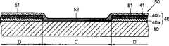
作为热处理的结果,如图4所示,一金属诱导结晶(MIC)区31通过使用包含在功能薄膜20上部、第二组分区域中的催化剂,或者使用单独在功能薄膜20上形成的结晶薄膜21直接诱导的结晶形成在未构图区域D上。一金属诱导横向结晶(MILC)区域32通过从MIC区域31的横向结晶形成在其中功能薄膜20的顶部、第二组分区域或者结晶薄膜21已被去除的图案区域C上。As a result of heat treatment, as shown in FIG. 21 Directly induced crystallization is formed on the unpatterned area D. A metal-induced lateral crystallization (MILC)
如图6中参考标号33所示,在与功能薄膜20的倾斜区域相对应的MIC区域31和MILC区域32之间的边界区域IV中,MIC区域31和MILC区域32同时出现。特别是,在靠近未构图区域D的中间区域E的区域中,由于剩余在功能薄膜20上部区域中的结晶催化剂的存在,非晶硅薄膜30就直接结晶成为MIC区域31。在靠近构图区域C的中间区域E的区域中,MILC32区域通过从MIC区域31的横向结晶而形成。其结果,在中间区域E中形成MIC和MILC结合区域33。此外,由于功能薄膜20包括在其厚度方向具有浓度梯度曲线的第一和第二组分,因此MILC区域32通过从MIC区域31的横向结晶逐渐形成,而在两个区域之间没有一个明确的边界。As shown by reference numeral 33 in FIG. 6 , in the boundary region IV between the
在使用上述方法将非晶硅薄膜结晶为一多晶硅薄膜后,就可由该多晶硅薄膜制造一薄膜晶体管(TFT)。After the amorphous silicon film is crystallized into a polysilicon film by the method described above, a thin film transistor (TFT) can be fabricated from the polysilicon film.
根据本发明一个实施例的TFT包括一半导体有源层、一在半导体有源层上形成的栅极介电层、和一在栅极介电层上形成的栅电极。该半导体有源层包括一沟道区、源极区和漏极区,源极区和漏极区通过掺杂高浓度的杂质离子在沟道区的相应侧形成。A TFT according to an embodiment of the present invention includes a semiconductor active layer, a gate dielectric layer formed on the semiconductor active layer, and a gate electrode formed on the gate dielectric layer. The semiconductor active layer includes a channel region, a source region and a drain region, and the source region and the drain region are formed on corresponding sides of the channel region by doping high-concentration impurity ions.
半导体有源层是由本发明的多晶硅薄膜形成。参考图6,在构图区域C中的MILC区域32形成一沟道区,在未构图区域D中的MIC区域31和中间区域E中的MIC和MILC结合区域33的结合在沟道区的两侧形成源极区和漏极区。因此,外部光吸收层,即,由剩余在未构图D和中间区域E中的功能薄膜20形成的黑色基质存在于衬底10和半导体有源层的至少源极区和漏极区之间。功能薄膜20还剩余在衬底10和沟道区之间。但是,剩余在沟道区下面与MILC区域32对应的功能薄膜20仅包含透明第一组分,因此,它不能用作光吸收黑色基质。The semiconductor active layer is formed of the polysilicon thin film of the present invention. With reference to Fig. 6, the
在由多晶硅薄膜形成半导体有源层后,就在该半导体有源层上顺序形成一栅极介电层和一栅电极。然后,用高浓度杂质离子掺杂源极区和漏极区。After the semiconductor active layer is formed from the polysilicon film, a gate dielectric layer and a gate electrode are sequentially formed on the semiconductor active layer. Then, the source region and the drain region are doped with high-concentration impurity ions.
在形成这样的TFT之后,还可以在栅电极上形成一个层间绝缘层。在源电极和漏电极可通过在层间绝缘层中形成的接触孔而形成的情况下,形成一钝化层以覆盖源电极和漏电极,并形成与漏电极电连接的像素电极。而且,一平整层可形成在所得到的结构上。源电极和漏电极可形成各种形状而不受本实施例的限制。After forming such a TFT, an interlayer insulating layer may also be formed on the gate electrode. In case the source electrode and the drain electrode can be formed through the contact hole formed in the interlayer insulating layer, a passivation layer is formed to cover the source electrode and the drain electrode, and a pixel electrode electrically connected to the drain electrode is formed. Also, a leveling layer can be formed on the resulting structure. The source and drain electrodes can be formed in various shapes without being limited by this embodiment.
根据所需显示器件的特征,可使用各种方法形成这样一种由根据本发明的一种方法形成的多晶硅薄膜形成的TFT。Such a TFT formed of a polysilicon film formed by a method according to the present invention may be formed using various methods depending on the characteristics of a desired display device.
在制造一种用于向后发光型显示器的TFT时,构图黑色基质用于暴露像素的开口能够与构图功能薄膜20同时进行,以形成一个将成为多晶硅MILC区的区域,即,一个半导体有源层的沟道区,由此能够减少工艺操作过程的数量。In the manufacture of a TFT for a rear-emitting display, patterning the black matrix for exposing the pixel openings can be performed simultaneously with patterning the
如上所述根据本发明制造的TFT能够用于各种平板显示器件,如LCD及有机和无机LED。TFTs fabricated according to the present invention as described above can be used in various flat panel display devices such as LCDs and organic and inorganic LEDs.
图9是表示一种根据本发明一个实施例使用了由上述方法形成的TFT的有源矩阵有机发光显示器(AMOLED)。FIG. 9 is a diagram illustrating an active matrix organic light emitting display (AMOLED) using TFTs formed by the above method according to an embodiment of the present invention.
参考图9,在透明衬底100上形成一包括透明像素电极的像素区200和一包括TFT及一电容的驱动区300。在衬底100的上表面可直接形成一由SiOx(x≥1)或SiNx(x≥1)制成的附加缓冲层(未图示)。Referring to FIG. 9 , a
在驱动区300中,一半导体有源层302是由一作为衬底100的上表面上的预定图案的多晶硅薄膜形成的,形成一栅极介电层303以覆盖半导体有源层302。一栅电极层304形成在半导体有源层302上面的栅极介电层303上,以及形成一覆盖栅电极层304的层间绝缘层305。穿过层间绝缘层305和栅极介电层303形成接触孔306a和307a,在层间绝缘层305上形成的漏电极306和源电极307通过接触孔306a和307a分别与半导体有源层302的漏极区302b和源极区302c相连接。在驱动区300中形成一电容器310,该电容器310包括第一电极311和第二电极312,并具有设置在两电极之间的层间绝缘层305,其中第一电极311与源电极307相连接。In the driving
在驱动区300的TFT和电容器310以及像素区200上形成一钝化层308,在其上形成一具有一暴露像素区200的开口的平整层309。与TFT的漏电极306电连接的透明电极202位于平面层309的开口下面。一有机层204沉积在透明电极202上,一阴极层206形成在有机层204和平整层309的整个表面上。A
在上述的显示器中,一阻挡外部光反射的黑色基质层110直接形成在衬底100的表面上。如图9所示,该黑色基质层110具有一个在像素区200下面具有开口112和在半导体有源层302的沟道区302a下面具有开口114的预定图案。开口112允许光穿过像素区200,开口114从沟道区302a诱导横向结晶以形成一MILC区域。暴露显示器的像素区200的开口112和暴露TFT的沟道区302a的开口114能够通过一单个构图操作而同时形成,以便简化全部制造的操作过程。In the above-mentioned display, a
根据上述本发明的非晶硅的结晶方法还能与Cr/CrOx薄膜兼容,这种Cr/CrOx薄膜通常用于形成显示器的黑色基质。The crystallization method of amorphous silicon according to the present invention described above is also compatible with Cr/CrOx films, which are commonly used to form black matrices for displays.
图10至12表示根据本发明的另一个实施例的非晶硅的一种结晶方法。10 to 12 show a crystallization method of amorphous silicon according to another embodiment of the present invention.
参考图10,一例如由CrOx(x≥1)制成的第一薄膜40a和一例如由Cr制成的第二薄膜40b形成在绝缘衬底10上作为一功能薄膜40。功能薄膜40可用作一黑色基质。由于第二薄膜40b是由Cr形成,因此就无需在功能薄膜40上形成一附加结晶薄膜。但是,对硅结晶更有效的一种催化剂,如Ni或Pb可结合在第二薄膜40b的上部区域中。而且,具有这样的一种硅结晶催化剂的结晶薄膜41可另外形成在第二薄膜40b的表面上。此外,一由例如SiOx(x≥1)或SiNx(x≥1)制成的附加缓冲层可在衬底10和第一薄膜40a之间形成。Referring to FIG. 10, a
如图11所示,功能薄膜40在构图后形成。在功能薄膜40用作显示器的外部光吸收层的情况下,该构图工艺可与一暴露显示器像素区的构图同时进行。其结果,如上所述,该显示器能用较少的制造操作过程完成。As shown in FIG. 11, the functional
作为构图的结果,功能薄膜40具有一构图区C和一未构图区D。由于功能薄膜40在其厚度方向不具有浓度梯度曲线,与前面的实施例不同,在构图区C和未构图区D之间的边界外不形成一倾斜区域。相反,由于第一薄膜40a的CrOx(x≥1)和第二薄膜40b的Cr之间的蚀刻速率差,在构图区C和未构图区D之间存在一个陡台阶。构图区C和未构图区D之间的这种台阶可被有意诱导。The
然后,在功能薄膜40的构图区C和未构图区D上形成一非晶硅薄膜50,如图12所示,该非晶硅薄膜50进行结晶热处理。结果是,由于通过Cr或第一薄膜40b中的硅结晶催化剂,或者通过结晶薄膜41诱导的非晶硅薄膜50的结晶,在未构图区D中形成一MIC区域51。此外,由于从MIC区域51的横向结晶在构图区D中形成一MILC区域52。在本实施例中,与前面实施例不同,没有形成MIC和MILC的结合区。但是,在非晶硅薄膜50沉积后,根据在构图区C和未构图区D之间的边界产生的台阶可存在一MIC和MILC结合区的较小延伸段。Then, an
在形成多晶硅薄膜后,虽然未图示,但是一沟道区可在MILC区域52的中心区限定,一源极区和一漏极区可在MILC区域52和MIC区域51的外围区域限定,其中,沟道区、源极区和漏极区形成一半导体有源层。为了提供一完整的TFT,虽然未图示,但是一栅极介电层和一栅电极可在半导体有源层上形成,之后将高浓度杂质离子注入源极区和漏极区,正如上面参考图9所述。After forming the polysilicon film, although not shown, a channel region can be defined in the central region of the
虽然附图中未显示,但是除了如上所述的Cr和CrOx层结合外,单个Cr或CrOx层,或者一通常的石墨黑色基质能够用作黑色基质。在使用通常的石墨黑色基质的情况下,一硅结晶催化剂可加入该石墨黑色基质的上部区域中,或者在该石墨黑色基质上形成一附加结晶薄膜。此外,用于黑色基质的石墨物质需要在结晶温度的热耐久性。Although not shown in the drawings, instead of the combination of Cr andCrOx layers as described above, a single Cr orCrOx layer, or a generally graphite black matrix can be used as the black matrix. In the case of a conventional graphite black matrix, a silicon crystallization catalyst can be added in the upper region of the graphite black matrix, or an additional crystalline film can be formed on the graphite black matrix. In addition, graphite materials used for black matrices require thermal durability at the crystallization temperature.
根据本发明,如上所述,使用一黑色基质层以比较简单的方式能够使非晶硅薄膜进行结晶,以此消除了复杂的操作而在MILC区域中限定一沟道区。此外,一限定TFT的MILC区的区域和一暴露显示器像素的区域通过一单个构图操作而能在该黑色基质中限定,因此减少了所需制造操作过程的数量。According to the present invention, as described above, an amorphous silicon thin film can be crystallized in a relatively simple manner using a black matrix layer, thereby eliminating complicated operations to define a channel region in the MILC region. Furthermore, an area defining the MILC region of the TFT and an area exposing the display pixels can be defined in the black matrix by a single patterning operation, thus reducing the number of required manufacturing operations.
虽然上面已经显示和描述了本发明的一些实施例,但是本领域的技术人员应该明白,在不脱离本发明的原则和精神及权利要求限定的保护范围和其等效范围的前提下可对实施例作出修改。Although some embodiments of the present invention have been shown and described above, those skilled in the art should understand that, on the premise of not departing from the principle and spirit of the present invention and the protection scope defined by the claims and its equivalent scope, the Example modification.
Claims (20)
Translated fromChineseApplications Claiming Priority (3)
| Application Number | Priority Date | Filing Date | Title |
|---|---|---|---|
| KR45955/2002 | 2002-08-03 | ||
| KR10-2002-0045955AKR100496287B1 (en) | 2002-08-03 | 2002-08-03 | Crystallizing method of silicon thin film, TFT used the method and flat panel display device with the TFT |
| KR45955/02 | 2002-08-03 |
Publications (2)
| Publication Number | Publication Date |
|---|---|
| CN1494107A CN1494107A (en) | 2004-05-05 |
| CN1288715Ctrue CN1288715C (en) | 2006-12-06 |
Family
ID=32026029
Family Applications (1)
| Application Number | Title | Priority Date | Filing Date |
|---|---|---|---|
| CNB031580971AExpired - LifetimeCN1288715C (en) | 2002-08-03 | 2003-08-01 | Silicon film crystallization method, thin film transistor using said method and its plate display |
Country Status (4)
| Country | Link |
|---|---|
| US (1) | US6864130B2 (en) |
| JP (1) | JP4204909B2 (en) |
| KR (1) | KR100496287B1 (en) |
| CN (1) | CN1288715C (en) |
Cited By (1)
| Publication number | Priority date | Publication date | Assignee | Title |
|---|---|---|---|---|
| CN105374846A (en)* | 2014-08-14 | 2016-03-02 | 乐金显示有限公司 | Organic light emitting display panel |
Families Citing this family (28)
| Publication number | Priority date | Publication date | Assignee | Title |
|---|---|---|---|---|
| KR100466628B1 (en) | 2002-11-12 | 2005-01-15 | 삼성에스디아이 주식회사 | Flat panel display and fabrication method thereof |
| KR100552975B1 (en)* | 2003-11-22 | 2006-02-15 | 삼성에스디아이 주식회사 | Active matrix organic light emitting display device and manufacturing method thereof |
| US7170176B2 (en) | 2003-11-04 | 2007-01-30 | Semiconductor Energy Laboratory Co., Ltd. | Semiconductor device |
| KR100600853B1 (en)* | 2003-11-17 | 2006-07-14 | 삼성에스디아이 주식회사 | Flat panel display and manufacturing method |
| KR100712112B1 (en)* | 2004-06-30 | 2007-04-27 | 삼성에스디아이 주식회사 | Semiconductor device and manufacturing method thereof |
| KR100659759B1 (en)* | 2004-10-06 | 2006-12-19 | 삼성에스디아이 주식회사 | Bottom gate thin film transistor, flat panel display device having same, and manufacturing method of thin film transistor |
| JP4554330B2 (en)* | 2004-10-21 | 2010-09-29 | 株式会社リコー | High durability heat insulating stamper structure |
| US7309895B2 (en) | 2005-01-25 | 2007-12-18 | Hewlett-Packard Development Company, L.P. | Semiconductor device |
| CN100592174C (en)* | 2005-05-21 | 2010-02-24 | 香港科技大学 | Transflective liquid crystal device and preparation method thereof |
| KR100709104B1 (en) | 2006-04-13 | 2007-04-18 | 주식회사 테라세미콘 | Polycrystalline Silicon Thin Film Manufacturing Method |
| KR101035752B1 (en)* | 2005-11-30 | 2011-05-20 | 사천홍시현시기건유한공사 | Polycrystalline Silicon Thin Film Transistor and Manufacturing Method Thereof |
| KR100742380B1 (en)* | 2005-12-28 | 2007-07-24 | 삼성에스디아이 주식회사 | Mask pattern, thin film transistor manufacturing method and organic electroluminescent display device manufacturing method using same |
| CN100433260C (en)* | 2006-01-16 | 2008-11-12 | 中华映管股份有限公司 | Method for manufacturing polycrystalline silicon layer and thin film transistor |
| KR100864883B1 (en)* | 2006-12-28 | 2008-10-22 | 삼성에스디아이 주식회사 | A thin film transistor, a manufacturing method thereof, and an organic light emitting display device having the same. |
| KR100822216B1 (en)* | 2007-04-09 | 2008-04-16 | 삼성에스디아이 주식회사 | A thin film transistor substrate, an organic light emitting display including the same, and a method of manufacturing an organic light emitting display |
| KR100837281B1 (en)* | 2007-05-23 | 2008-06-11 | 삼성전자주식회사 | Semiconductor device package and manufacturing method thereof |
| KR100893488B1 (en)* | 2008-02-28 | 2009-04-17 | 삼성모바일디스플레이주식회사 | LCD Display |
| KR101545315B1 (en) | 2008-09-17 | 2015-08-20 | 삼성디스플레이 주식회사 | Organic electroluminescent device |
| KR101084242B1 (en)* | 2010-01-14 | 2011-11-16 | 삼성모바일디스플레이주식회사 | Organic light emitting display and manufacturing method thereof |
| KR101064325B1 (en)* | 2010-05-24 | 2011-09-14 | 노코드 주식회사 | Method of manufacturing polycrystalline silicon thin film |
| CN102709184B (en)* | 2011-05-13 | 2016-08-17 | 京东方科技集团股份有限公司 | Thin film transistor (TFT), its manufacture method and array base palte containing polysilicon active layer |
| KR20130006945A (en) | 2011-06-27 | 2013-01-18 | 삼성디스플레이 주식회사 | Flat panel display device and the manufacturing method thereof |
| KR20140023492A (en)* | 2012-08-16 | 2014-02-27 | 삼성코닝정밀소재 주식회사 | Sputtering target and organic light emitting diode display device including black matrix deposited by the same |
| TWI566395B (en)* | 2013-11-18 | 2017-01-11 | 元太科技工業股份有限公司 | Organic light emitting diode display and manufacturing method thereof |
| CN108122924B (en)* | 2016-10-31 | 2021-01-26 | 中芯国际集成电路制造(北京)有限公司 | Flash memory device and method of manufacturing the same |
| TWI648879B (en)* | 2018-04-11 | 2019-01-21 | 友達光電股份有限公司 | Light-emitting element |
| KR102850623B1 (en) | 2020-12-24 | 2025-08-26 | 삼성디스플레이 주식회사 | Display apparatus |
| KR102470876B1 (en)* | 2021-01-28 | 2022-11-25 | 재단법인대구경북과학기술원 | Method for high crystallization of upper layer of a Monolithc 3D device and Monolithc 3D device manufactured by the same |
Family Cites Families (5)
| Publication number | Priority date | Publication date | Assignee | Title |
|---|---|---|---|---|
| JP3390579B2 (en)* | 1995-07-03 | 2003-03-24 | アネルバ株式会社 | Method and apparatus for producing thin film for liquid crystal display |
| JP2000208771A (en)* | 1999-01-11 | 2000-07-28 | Hitachi Ltd | Semiconductor device, liquid crystal display device, and manufacturing method thereof |
| KR20020035909A (en)* | 2000-11-07 | 2002-05-16 | 한민구 | Manufacturing Process of Polycrystalline Silicon Thin Film Transistor |
| KR20020036916A (en)* | 2000-11-11 | 2002-05-17 | 주승기 | Method of crystallizing a silicon thin film and semiconductor device fabricated thereby |
| US6566687B2 (en)* | 2001-01-18 | 2003-05-20 | International Business Machines Corporation | Metal induced self-aligned crystallization of Si layer for TFT |
- 2002
- 2002-08-03KRKR10-2002-0045955Apatent/KR100496287B1/ennot_activeExpired - Lifetime
- 2003
- 2003-06-27JPJP2003184563Apatent/JP4204909B2/ennot_activeExpired - Lifetime
- 2003-07-23USUS10/624,636patent/US6864130B2/ennot_activeExpired - Lifetime
- 2003-08-01CNCNB031580971Apatent/CN1288715C/ennot_activeExpired - Lifetime
Cited By (2)
| Publication number | Priority date | Publication date | Assignee | Title |
|---|---|---|---|---|
| CN105374846A (en)* | 2014-08-14 | 2016-03-02 | 乐金显示有限公司 | Organic light emitting display panel |
| US10079276B2 (en) | 2014-08-14 | 2018-09-18 | Lg Display Co., Ltd. | Organic light emitting display panel comprising pixel repair region |
Also Published As
| Publication number | Publication date |
|---|---|
| JP4204909B2 (en) | 2009-01-07 |
| JP2004072092A (en) | 2004-03-04 |
| KR100496287B1 (en) | 2005-06-20 |
| CN1494107A (en) | 2004-05-05 |
| US6864130B2 (en) | 2005-03-08 |
| US20040125265A1 (en) | 2004-07-01 |
| KR20040012391A (en) | 2004-02-11 |
Similar Documents
| Publication | Publication Date | Title |
|---|---|---|
| CN1288715C (en) | Silicon film crystallization method, thin film transistor using said method and its plate display | |
| CN108054192B (en) | Flexible AMOLED substrate and manufacturing method thereof | |
| CN1311563C (en) | Thin film transistor and method for manufacturing the same | |
| CN102280466B (en) | Display device and manufacture method thereof | |
| CN1271891C (en) | Electroluminescence display device and its making method | |
| CN102479752B (en) | Thin film transistor and active matrix rear panel as well as manufacturing methods thereof and display | |
| KR101213707B1 (en) | Poly Silicon Thin Film Transistor and Method of fabricating the same | |
| CN1913146A (en) | Thin film conductor and method of manufacturing the same | |
| CN1383214A (en) | Polysilicon film transistor of liquid crystal display device and its mfg. method | |
| CN103839825A (en) | Low-temperature polycrystalline silicon thin film transistor, array substrate and manufacturing method of array substrate | |
| CN1828832A (en) | Laser device and method for manufacturing thin film transistors therewith | |
| CN1183604C (en) | Thin film transistor and its manufacturing method and semiconductor device of said transistor | |
| CN1630027A (en) | Mask for crystallization, crystallization method, and method of manufacturing thin film transistor array panel including the crystallization method | |
| CN1501437A (en) | Mask for polycrystallization and method of manufacturing thin film transistor using same | |
| CN112864174A (en) | TFT array substrate, preparation method thereof and display device | |
| CN1638022A (en) | Method for forming polycrystalline silicon film | |
| WO2018201709A1 (en) | Thin film transistor, manufacturing method therefor, array substrate, and display device | |
| CN1637474A (en) | Liquid crystal display device and method of fabricating the same | |
| JP6040438B2 (en) | Thin film forming substrate and thin film forming method | |
| CN1251331C (en) | Semiconductor device | |
| CN1655056A (en) | Optical mask and method of manufacturing thin film transistor array panel using same | |
| CN1794069A (en) | Thin film transistor array panel | |
| CN1734334A (en) | Liquid crystal display device and manufacturing method thereof | |
| KR101457705B1 (en) | Fabricating method of electric device | |
| CN1324388C (en) | Manufacturing method of low temperature polysilicon thin film transistor liquid crystal display |
Legal Events
| Date | Code | Title | Description |
|---|---|---|---|
| C06 | Publication | ||
| PB01 | Publication | ||
| C10 | Entry into substantive examination | ||
| SE01 | Entry into force of request for substantive examination | ||
| C14 | Grant of patent or utility model | ||
| GR01 | Patent grant | ||
| ASS | Succession or assignment of patent right | Owner name:SAMSUNG DISPLAY CO., LTD. Free format text:FORMER OWNER: SAMSUNG MOBILE DISPLAY CO., LTD. Effective date:20120928 | |
| C41 | Transfer of patent application or patent right or utility model | ||
| TR01 | Transfer of patent right | Effective date of registration:20120928 Address after:Gyeonggi Do Korea Suwon Patentee after:SAMSUNG DISPLAY Co.,Ltd. Address before:Gyeonggi Do Korea Suwon Patentee before:Samsung Mobile Display Co.,Ltd. | |
| CX01 | Expiry of patent term | Granted publication date:20061206 | |
| CX01 | Expiry of patent term |