CN1287585C - Scanning camera - Google Patents
Scanning cameraDownload PDFInfo
- Publication number
- CN1287585C CN1287585CCNB02816945XACN02816945ACN1287585CCN 1287585 CCN1287585 CCN 1287585CCN B02816945X ACNB02816945X ACN B02816945XACN 02816945 ACN02816945 ACN 02816945ACN 1287585 CCN1287585 CCN 1287585C
- Authority
- CN
- China
- Prior art keywords
- photoelectric sensor
- micro
- reflector
- camera
- mirror
- Prior art date
- Legal status (The legal status is an assumption and is not a legal conclusion. Google has not performed a legal analysis and makes no representation as to the accuracy of the status listed.)
- Expired - Fee Related
Links
- 239000005357flat glassSubstances0.000claims2
- 230000003287optical effectEffects0.000abstractdescription2
- 239000011521glassSubstances0.000description3
- XUIMIQQOPSSXEZ-UHFFFAOYSA-NSiliconChemical compound[Si]XUIMIQQOPSSXEZ-UHFFFAOYSA-N0.000description2
- 239000013256coordination polymerSubstances0.000description2
- 230000002441reversible effectEffects0.000description2
- 229910052710siliconInorganic materials0.000description2
- 239000010703siliconSubstances0.000description2
- 239000003086colorantSubstances0.000description1
- 238000010276constructionMethods0.000description1
- 238000010586diagramMethods0.000description1
- 238000000034methodMethods0.000description1
- 239000004065semiconductorSubstances0.000description1
- 239000007787solidSubstances0.000description1
- 239000000758substrateSubstances0.000description1
Images


Classifications
- H—ELECTRICITY
- H04—ELECTRIC COMMUNICATION TECHNIQUE
- H04N—PICTORIAL COMMUNICATION, e.g. TELEVISION
- H04N3/00—Scanning details of television systems; Combination thereof with generation of supply voltages
- H04N3/02—Scanning details of television systems; Combination thereof with generation of supply voltages by optical-mechanical means only
- H04N3/08—Scanning details of television systems; Combination thereof with generation of supply voltages by optical-mechanical means only having a moving reflector
Landscapes
- Engineering & Computer Science (AREA)
- Multimedia (AREA)
- Signal Processing (AREA)
- Studio Devices (AREA)
- Mechanical Light Control Or Optical Switches (AREA)
- Transforming Light Signals Into Electric Signals (AREA)
Abstract
Translated fromChinese
Description
Translated fromChinese技术领域technical field
本发明涉及所谓扫描摄像机。The invention relates to so-called scanning cameras.
背景技术Background technique
目前,在电子摄像机或数字摄像机、摄录机和可视电话中所使用的光电图象传感器都是以具有光敏元件(所谓象素)阵列的半导体芯片为基础。为了在这种传感器上形成目标图象,设置了在最简情况下由单个透镜组成的透镜系统。这种透镜系统具有畸变,因而需要进行清晰度调整或将其限制在预定的固定距离范围内,从而限制了它们的分辨率。Photoelectric image sensors currently used in electronic or digital video cameras, camcorders and videophones are based on semiconductor chips having an array of light-sensitive elements, so-called pixels. In order to form an object image on such a sensor, a lens system consisting of a single lens in the simplest case is provided. Such lens systems have distortions that require sharpness adjustments or are limited to a predetermined fixed distance, limiting their resolution.
上面所提到的一些设备的制造商都在致力于减轻重量、减小结构体积和降低成本。透镜焦距和透镜与图像传感器的距离由传感器的对角线的摄像机的摄像角预先给定。通过减小传感器对角线因而减小象素尺寸实现进一步小型化,需要价格高得多的更加昂贵的透镜系统。Manufacturers of some of the above-mentioned devices are striving to reduce weight, construction volume and cost. The focal length of the lens and the distance of the lens from the image sensor are predetermined by the angle of view of the camera at the diagonal of the sensor. Further miniaturization by reducing the sensor diagonal and thus the pixel size requires a much more expensive lens system at a much higher price.
发明内容Contents of the invention
本发明的任务旨在提供一种尺寸较小且成本低的摄像机。The object of the present invention is to provide a video camera that is small in size and low in cost.
根据本发明,这个任务已由权利要求书中所指出的一些特征加以解决。According to the invention, this task is solved by some of the features indicated in the claims.
根据本发明的摄像机中,不再需要透镜,所有光学特性均得到显著改善。In the video camera according to the invention, lenses are no longer required, and all optical properties are significantly improved.
将根据本发明的扫描摄像机与带有透镜和传感器阵列的普通摄像机相比较,结构体积大大减小。Comparing the scanning camera according to the invention with a conventional camera with lens and sensor array, the structural volume is greatly reduced.
附图说明Description of drawings
下面,依据附图中所示的实施方案对本发明进行说明,在图中:Below, the present invention is described according to the embodiment shown in the accompanying drawing, in the figure:
图1示出根据本发明的扫描摄像机的原理图,Figure 1 shows a schematic diagram of a scanning camera according to the invention,
图2和图3示出在此所应用的微反射镜的实施形式,以及Figures 2 and 3 show embodiments of the micromirrors used here, and
图4示出在一个芯片上实现根据本发明的扫描摄像机。Figure 4 shows the implementation of a scanning camera according to the invention on one chip.
具体实施方式Detailed ways
根据本发明的扫描摄像机(SC)利用了一种新颖摄像系统。原则上,一种双轴可翻转或可回转的微反射镜能以帧方式对周围环境或对目标扫描,且能将光束控制到一个例如单个光探测元件或光电传感器上。The scanning camera (SC) according to the invention utilizes a novel camera system. In principle, a two-axis reversible or rotatable micromirror can scan the surrounding environment or the target in a frame-wise manner, and can steer the light beam to a single photodetection element or photoelectric sensor, for example.
如图1所示,根据本发明的扫描摄像机SC具有点状光电传感器SE。该传感器SE由一个元件或一个象素组成。特别是,在彩色摄像机的情况下,可能设置对不同彩色灵敏的多个象素。光电传感器SE例如能由一个光电晶体管、一个电荷耦合器件(CCD)芯片或由一个CMOS模块来实现。As shown in FIG. 1, the scanning camera SC according to the invention has a point photoelectric sensor SE. The sensor SE consists of one element or one pixel. In particular, in the case of color cameras, it is possible to provide a plurality of pixels sensitive to different colors. The photosensor SE can be realized, for example, by a phototransistor, a charge-coupled device (CCD) chip or by a CMOS module.
此外,扫描摄像机SC还具有一个由微反射镜SP实现的偏转单元。根据本发明,微反射镜SP对目标OB进行二维扫描。为此,微反射镜做成双轴可翻转式。这两个翻转轴首先应相互垂直。这种翻转运动在图1中由两个双箭头(未详细标明)用符号表示。被扫描的立体角被偏转或反射到传感器SE上。由此,以时分复用方法扫描要摄取图象的所有元件,并由传感器SE变换成图象数据。Furthermore, the scanning camera SC has a deflection unit realized by a micromirror SP. According to the present invention, the micro mirror SP scans the object OB two-dimensionally. For this reason, the micro-mirror is made into a biaxial reversible type. The two flip axes should first of all be perpendicular to each other. This pivoting movement is symbolized in FIG. 1 by two double arrows (not shown in detail). The scanned solid angle is deflected or reflected onto the sensor SE. Thus, all elements to be imaged are scanned in a time-multiplexed manner and converted into image data by the sensor SE.
偏转单元或微反射镜SP例如可以由所谓微机械元件(MEMS装置)来实现。有关这类结构元件的概况可以通过互联网访问URL所属的网址http://mems.colorado.edu/cl。res.ppt/ppt/oe.review查询。The deflection unit or micromirror SP can be realized, for example, by a so-called micromechanical element (MEMS device). An overview of such structural elements can be accessed via the Internet under the URL http://mems.colorado.edu/cl. res.ppt/ppt/oe.review query.
对于根据本发明的扫描摄像机SC来说,光敏传感器SE被减小到仅有一个唯一的象点,其中按时分复用拍摄了所要拍摄的图象或目标OB的所有要素。由原理决定可以放弃准直透镜系统,因此也取消了对图象距离的聚焦。In the scanning camera SC according to the invention, the photosensitive sensor SE is reduced to a single pixel in which all elements of the image to be recorded or the object OB are recorded time-multiplexed. The principle dictates that the collimating lens system can be dispensed with, thus also canceling the focusing on the image distance.
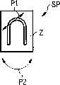
图2示出一种用微机械元件可能实现的微反射镜SP形式。微机械元件主要由硅构成,由硅刻蚀出可运动的舌片Z。舌片Z例如可能以约30~40KHz的频率偏转到与图面垂直。这个运动方向用双箭头P1以符号表示。此外,图2中所示微反射镜SP还可以例如以50Hz频率在图面内旋转。这个运动方向用双箭头P2以符号表示。Figure 2 shows a possible implementation of micromirror SP with micromechanical components. The micromechanical components are mainly made of silicon, from which the movable tongue Z is etched. The tongue Z may, for example, be deflected perpendicular to the drawing plane at a frequency of about 30-40 KHz. This direction of movement is symbolized by a double arrow P1. Furthermore, the micromirror SP shown in FIG. 2 can also be rotated within the drawing plane, for example at a frequency of 50 Hz. This direction of movement is symbolized by a double arrow P2.
图3中示出微反射镜SP的另一个实现可能性。反射镜元件SPM是这样在两个侧面上呈运动状态与硅基体相连接,使元件SPM能以二维方式偏转。振频频率例如与图2中的相同。Another realization possibility of the micromirror SP is shown in FIG. 3 . The mirror element SPM is connected to the silicon substrate in a movable state on both sides in such a way that the element SPM can be deflected in two dimensions. The vibration frequency is, for example, the same as in FIG. 2 .
图4中示出根据本发明的扫描摄像机SC的一种特别优选的实施形式。在这种情况下,微反射镜SP和光电传感器SE被安排在一个平面内。微反射镜SP和光电传感器SE例如可以作为微机械元件并列制作在一个集成模块即芯片CP上。A particularly preferred embodiment of a scanning camera SC according to the invention is shown in FIG. 4 . In this case, the micromirror SP and the photosensor SE are arranged in one plane. The micromirror SP and the photoelectric sensor SE can be fabricated side by side as micromechanical elements on an integrated module, ie, the chip CP, for example.
为了使从微反射镜SP反射的光束LS转向传感器SE,安排了偏转反射镜US。In order to divert the light beam LS reflected from the micromirror SP towards the sensor SE, a deflection mirror US is arranged.
芯片CP可以安放在外罩GH的空间内,开口用玻璃片GP盖住,然后,将经玻璃片GP投射到反射镜SP上的光束LS经偏转反射镜SP偏转到传感器SE上。在这种情况下,偏转反射镜优选地由玻璃片GP的局部形成反射镜面来实现。The chip CP can be placed in the space of the outer cover GH, and the opening is covered with a glass plate GP. Then, the light beam LS projected on the mirror SP through the glass plate GP is deflected to the sensor SE by the deflecting mirror SP. In this case, the deflection mirror is preferably realized by a partially formed mirror surface of the glass pane GP.
Claims (3)
Applications Claiming Priority (2)
| Application Number | Priority Date | Filing Date | Title |
|---|---|---|---|
| DE10141908 | 2001-08-28 | ||
| DE10141908.2 | 2001-08-28 |
Publications (2)
| Publication Number | Publication Date |
|---|---|
| CN1550099A CN1550099A (en) | 2004-11-24 |
| CN1287585Ctrue CN1287585C (en) | 2006-11-29 |
Family
ID=7696739
Family Applications (1)
| Application Number | Title | Priority Date | Filing Date |
|---|---|---|---|
| CNB02816945XAExpired - Fee RelatedCN1287585C (en) | 2001-08-28 | 2002-07-23 | Scanning camera |
Country Status (5)
| Country | Link |
|---|---|
| US (1) | US20040207744A1 (en) |
| EP (1) | EP1421779A1 (en) |
| JP (1) | JP4018631B2 (en) |
| CN (1) | CN1287585C (en) |
| WO (1) | WO2003028363A1 (en) |
Families Citing this family (17)
| Publication number | Priority date | Publication date | Assignee | Title |
|---|---|---|---|---|
| IL165212A (en) | 2004-11-15 | 2012-05-31 | Elbit Systems Electro Optics Elop Ltd | Device for scanning light |
| FI118245B (en)* | 2005-06-08 | 2007-08-31 | Iprbox Oy | Camera |
| WO2008068735A2 (en)* | 2006-12-03 | 2008-06-12 | Maradin Technologies Ltd. | A gimbaled scanning micro-mirror actuation scheme and architecture |
| WO2009147654A1 (en)* | 2008-06-02 | 2009-12-10 | Maradin Technologies Ltd. | Gimbaled scanning micro-mirror apparatus |
| EP2435355B1 (en)* | 2009-05-29 | 2018-10-24 | DigitalOptics Corporation MEMS | Mechanical isolation for mems electrical contacts |
| US9253360B2 (en) | 2011-07-15 | 2016-02-02 | Ziva Corporation, Inc. | Imager |
| CN104160240B (en) | 2012-02-15 | 2017-02-22 | 苹果公司 | Scanning depth engine |
| EP2828833B1 (en) | 2012-03-22 | 2017-03-08 | Apple Inc. | Gimbaled scanning mirror array |
| WO2014016794A1 (en) | 2012-07-26 | 2014-01-30 | Primesense Ltd. | Dual-axis scanning mirror |
| WO2014064606A1 (en) | 2012-10-23 | 2014-05-01 | Primesense Ltd. | Production of micro-mechanical devices |
| US9835853B1 (en) | 2014-11-26 | 2017-12-05 | Apple Inc. | MEMS scanner with mirrors of different sizes |
| US9784838B1 (en) | 2014-11-26 | 2017-10-10 | Apple Inc. | Compact scanner with gimbaled optics |
| US9798135B2 (en) | 2015-02-16 | 2017-10-24 | Apple Inc. | Hybrid MEMS scanning module |
| US9703096B2 (en) | 2015-09-30 | 2017-07-11 | Apple Inc. | Asymmetric MEMS mirror assembly |
| US9897801B2 (en) | 2015-09-30 | 2018-02-20 | Apple Inc. | Multi-hinge mirror assembly |
| US10488652B2 (en) | 2016-09-21 | 2019-11-26 | Apple Inc. | Prism-based scanner |
| WO2021034371A1 (en) | 2019-08-18 | 2021-02-25 | Apple Inc. | Force-balanced micromirror with electromagnetic actuation |
Family Cites Families (16)
| Publication number | Priority date | Publication date | Assignee | Title |
|---|---|---|---|---|
| WO1991015792A1 (en)* | 1990-04-06 | 1991-10-17 | Martin Russell Harris | Confocal microscope |
| FR2703475A1 (en)* | 1993-03-30 | 1994-10-07 | Foulgoc Patrick | Miniaturised camera (picture-taking) and projection device |
| US5673139A (en)* | 1993-07-19 | 1997-09-30 | Medcom, Inc. | Microelectromechanical television scanning device and method for making the same |
| US5629790A (en)* | 1993-10-18 | 1997-05-13 | Neukermans; Armand P. | Micromachined torsional scanner |
| US5612736A (en)* | 1995-06-07 | 1997-03-18 | Nview Corporation | Stylus position sensing and digital camera with a digital micromirror device |
| US5907425A (en)* | 1995-12-19 | 1999-05-25 | The Board Of Trustees Of The Leland Stanford Junior University | Miniature scanning confocal microscope |
| US6025951A (en)* | 1996-11-27 | 2000-02-15 | National Optics Institute | Light modulating microdevice and method |
| US6075237A (en)* | 1998-07-29 | 2000-06-13 | Eastman Kodak Company | Image sensor cover with integral light shield |
| US6002507A (en)* | 1998-12-01 | 1999-12-14 | Xerox Corpoation | Method and apparatus for an integrated laser beam scanner |
| JP2000258699A (en)* | 1999-03-05 | 2000-09-22 | Olympus Optical Co Ltd | Direct viewing type confocal optical system |
| US6155490A (en)* | 1999-04-22 | 2000-12-05 | Intermec Ip Corp. | Microelectromechanical systems scanning mirror for a laser scanner |
| AU1459800A (en)* | 1999-10-29 | 2001-05-14 | Microvision, Inc. | Real time millimeter wave scanning imager |
| US6221687B1 (en)* | 1999-12-23 | 2001-04-24 | Tower Semiconductor Ltd. | Color image sensor with embedded microlens array |
| WO2001091193A2 (en)* | 2000-05-23 | 2001-11-29 | Atmel Corporation | Integrated ic chip package for electronic image sensor die |
| US8423110B2 (en)* | 2002-01-09 | 2013-04-16 | Boston Scientific Scimed, Inc. | Imaging device and related methods |
| JP4259979B2 (en)* | 2003-10-22 | 2009-04-30 | 新光電気工業株式会社 | Light transmissive cover, device provided with the same, and manufacturing method thereof |
- 2002
- 2002-07-23CNCNB02816945XApatent/CN1287585C/ennot_activeExpired - Fee Related
- 2002-07-23EPEP02754414Apatent/EP1421779A1/ennot_activeWithdrawn
- 2002-07-23USUS10/487,859patent/US20040207744A1/ennot_activeAbandoned
- 2002-07-23WOPCT/DE2002/002703patent/WO2003028363A1/enactiveApplication Filing
- 2002-07-23JPJP2003531730Apatent/JP4018631B2/ennot_activeExpired - Fee Related
Also Published As
| Publication number | Publication date |
|---|---|
| US20040207744A1 (en) | 2004-10-21 |
| JP2005504487A (en) | 2005-02-10 |
| WO2003028363A1 (en) | 2003-04-03 |
| JP4018631B2 (en) | 2007-12-05 |
| CN1550099A (en) | 2004-11-24 |
| EP1421779A1 (en) | 2004-05-26 |
Similar Documents
| Publication | Publication Date | Title |
|---|---|---|
| CN1287585C (en) | Scanning camera | |
| KR101713879B1 (en) | Auto-focus camera module with flexible printed circuit extension | |
| US8248497B2 (en) | Image sensor device with movable sensor | |
| CN113572918B (en) | Periscopic continuous light-variable module and corresponding multi-camera module | |
| KR102486426B1 (en) | Camera module | |
| CN110913096A (en) | Camera module and electronic equipment | |
| CN1317887C (en) | Photoelectric conversion device, and image pickup device and autofocus camers using the same | |
| KR102303135B1 (en) | Multi-aperture imaging device, imaging system, and method for providing a multi-aperture imaging device | |
| US20100045845A1 (en) | Stacked type camera module, method of manufacturing stacked type camera module, and imaging apparatus | |
| US20070040924A1 (en) | Cellular phone camera with three-dimensional imaging function | |
| EP4240003A1 (en) | Optical image stabilization driver device, camera module and electronic device | |
| JP3662625B2 (en) | Imaging system | |
| JPH10133247A (en) | Video camera shake prevention device | |
| US20240422439A1 (en) | Camera actuator and camera device comprising same | |
| US20220303438A1 (en) | Imaging lens driving module, camera module and electronic device | |
| JP3875660B2 (en) | Multi electrostatic camera module | |
| JP6664496B2 (en) | Image scanning device | |
| US20200243577A1 (en) | Systems and methods for imaging using mechanical scanning mechanisms | |
| EP1289273A1 (en) | Scanning camera | |
| CN108429872B (en) | Method for correcting image vignetting, imaging device and imaging system | |
| CN1542462A (en) | Lens array device | |
| JPS6316064B2 (en) | ||
| JPH11220664A (en) | Image input method, image input device, electronic camera | |
| CN100517049C (en) | camera device | |
| JP4314476B2 (en) | Imaging device |
Legal Events
| Date | Code | Title | Description |
|---|---|---|---|
| C06 | Publication | ||
| PB01 | Publication | ||
| C10 | Entry into substantive examination | ||
| SE01 | Entry into force of request for substantive examination | ||
| C14 | Grant of patent or utility model | ||
| GR01 | Patent grant | ||
| ASS | Succession or assignment of patent right | Owner name:NINGBO DELIN MACHINERY CO., LTD. Free format text:FORMER OWNER: DINGRUI IND + TRADE CO., LTD., NINGBO Effective date:20101102 | |
| C41 | Transfer of patent application or patent right or utility model | ||
| COR | Change of bibliographic data | Free format text:CORRECT: ADDRESS; FROM: 315010 18/F, TIANYUAN BUILDING, NO.9, JIEFANG SOUTH ROAD, HAISHU DISTRICT, NINGBO CITY, ZHEJIANG PROVINCE TO: 315020 NO.406, JIANGHU ROAD, INVESTMENT VENTURE PARK, JIANGBEI DISTRICT, NINGBO CITY | |
| TR01 | Transfer of patent right | Effective date of registration:20101108 Address after:Munich, Germany Patentee after:Siemens AG Address before:Munich, Germany Patentee before:Siemens AG | |
| C17 | Cessation of patent right | ||
| CF01 | Termination of patent right due to non-payment of annual fee | Granted publication date:20061129 Termination date:20120723 |