CN1286791A - Optical information recording medium and optical recording method - Google Patents
Optical information recording medium and optical recording methodDownload PDFInfo
- Publication number
- CN1286791A CN1286791ACN99801637ACN99801637ACN1286791ACN 1286791 ACN1286791 ACN 1286791ACN 99801637 ACN99801637 ACN 99801637ACN 99801637 ACN99801637 ACN 99801637ACN 1286791 ACN1286791 ACN 1286791A
- Authority
- CN
- China
- Prior art keywords
- recording
- linear velocity
- layer
- optical information
- area
- Prior art date
- Legal status (The legal status is an assumption and is not a legal conclusion. Google has not performed a legal analysis and makes no representation as to the accuracy of the status listed.)
- Granted
Links
Images


Classifications
- G—PHYSICS
- G11—INFORMATION STORAGE
- G11B—INFORMATION STORAGE BASED ON RELATIVE MOVEMENT BETWEEN RECORD CARRIER AND TRANSDUCER
- G11B7/00—Recording or reproducing by optical means, e.g. recording using a thermal beam of optical radiation by modifying optical properties or the physical structure, reproducing using an optical beam at lower power by sensing optical properties; Record carriers therefor
- G11B7/24—Record carriers characterised by shape, structure or physical properties, or by the selection of the material
- G11B7/241—Record carriers characterised by shape, structure or physical properties, or by the selection of the material characterised by the selection of the material
- G11B7/242—Record carriers characterised by shape, structure or physical properties, or by the selection of the material characterised by the selection of the material of recording layers
- G11B7/243—Record carriers characterised by shape, structure or physical properties, or by the selection of the material characterised by the selection of the material of recording layers comprising inorganic materials only, e.g. ablative layers
- G—PHYSICS
- G11—INFORMATION STORAGE
- G11B—INFORMATION STORAGE BASED ON RELATIVE MOVEMENT BETWEEN RECORD CARRIER AND TRANSDUCER
- G11B7/00—Recording or reproducing by optical means, e.g. recording using a thermal beam of optical radiation by modifying optical properties or the physical structure, reproducing using an optical beam at lower power by sensing optical properties; Record carriers therefor
- G11B7/004—Recording, reproducing or erasing methods; Read, write or erase circuits therefor
- G11B7/006—Overwriting
- G11B7/0062—Overwriting strategies, e.g. recording pulse sequences with erasing level used for phase-change media
- G—PHYSICS
- G11—INFORMATION STORAGE
- G11B—INFORMATION STORAGE BASED ON RELATIVE MOVEMENT BETWEEN RECORD CARRIER AND TRANSDUCER
- G11B7/00—Recording or reproducing by optical means, e.g. recording using a thermal beam of optical radiation by modifying optical properties or the physical structure, reproducing using an optical beam at lower power by sensing optical properties; Record carriers therefor
- G11B7/12—Heads, e.g. forming of the optical beam spot or modulation of the optical beam
- G11B7/125—Optical beam sources therefor, e.g. laser control circuitry specially adapted for optical storage devices; Modulators, e.g. means for controlling the size or intensity of optical spots or optical traces
- G11B7/126—Circuits, methods or arrangements for laser control or stabilisation
- G—PHYSICS
- G11—INFORMATION STORAGE
- G11B—INFORMATION STORAGE BASED ON RELATIVE MOVEMENT BETWEEN RECORD CARRIER AND TRANSDUCER
- G11B7/00—Recording or reproducing by optical means, e.g. recording using a thermal beam of optical radiation by modifying optical properties or the physical structure, reproducing using an optical beam at lower power by sensing optical properties; Record carriers therefor
- G11B7/24—Record carriers characterised by shape, structure or physical properties, or by the selection of the material
- G11B7/241—Record carriers characterised by shape, structure or physical properties, or by the selection of the material characterised by the selection of the material
- G11B7/242—Record carriers characterised by shape, structure or physical properties, or by the selection of the material characterised by the selection of the material of recording layers
- G11B7/243—Record carriers characterised by shape, structure or physical properties, or by the selection of the material characterised by the selection of the material of recording layers comprising inorganic materials only, e.g. ablative layers
- G11B2007/24302—Metals or metalloids
- G11B2007/24308—Metals or metalloids transition metal elements of group 11 (Cu, Ag, Au)
- G—PHYSICS
- G11—INFORMATION STORAGE
- G11B—INFORMATION STORAGE BASED ON RELATIVE MOVEMENT BETWEEN RECORD CARRIER AND TRANSDUCER
- G11B7/00—Recording or reproducing by optical means, e.g. recording using a thermal beam of optical radiation by modifying optical properties or the physical structure, reproducing using an optical beam at lower power by sensing optical properties; Record carriers therefor
- G11B7/24—Record carriers characterised by shape, structure or physical properties, or by the selection of the material
- G11B7/241—Record carriers characterised by shape, structure or physical properties, or by the selection of the material characterised by the selection of the material
- G11B7/242—Record carriers characterised by shape, structure or physical properties, or by the selection of the material characterised by the selection of the material of recording layers
- G11B7/243—Record carriers characterised by shape, structure or physical properties, or by the selection of the material characterised by the selection of the material of recording layers comprising inorganic materials only, e.g. ablative layers
- G11B2007/24302—Metals or metalloids
- G11B2007/2431—Metals or metalloids group 13 elements (B, Al, Ga, In)
- G—PHYSICS
- G11—INFORMATION STORAGE
- G11B—INFORMATION STORAGE BASED ON RELATIVE MOVEMENT BETWEEN RECORD CARRIER AND TRANSDUCER
- G11B7/00—Recording or reproducing by optical means, e.g. recording using a thermal beam of optical radiation by modifying optical properties or the physical structure, reproducing using an optical beam at lower power by sensing optical properties; Record carriers therefor
- G11B7/24—Record carriers characterised by shape, structure or physical properties, or by the selection of the material
- G11B7/241—Record carriers characterised by shape, structure or physical properties, or by the selection of the material characterised by the selection of the material
- G11B7/242—Record carriers characterised by shape, structure or physical properties, or by the selection of the material characterised by the selection of the material of recording layers
- G11B7/243—Record carriers characterised by shape, structure or physical properties, or by the selection of the material characterised by the selection of the material of recording layers comprising inorganic materials only, e.g. ablative layers
- G11B2007/24302—Metals or metalloids
- G11B2007/24312—Metals or metalloids group 14 elements (e.g. Si, Ge, Sn)
- G—PHYSICS
- G11—INFORMATION STORAGE
- G11B—INFORMATION STORAGE BASED ON RELATIVE MOVEMENT BETWEEN RECORD CARRIER AND TRANSDUCER
- G11B7/00—Recording or reproducing by optical means, e.g. recording using a thermal beam of optical radiation by modifying optical properties or the physical structure, reproducing using an optical beam at lower power by sensing optical properties; Record carriers therefor
- G11B7/24—Record carriers characterised by shape, structure or physical properties, or by the selection of the material
- G11B7/241—Record carriers characterised by shape, structure or physical properties, or by the selection of the material characterised by the selection of the material
- G11B7/242—Record carriers characterised by shape, structure or physical properties, or by the selection of the material characterised by the selection of the material of recording layers
- G11B7/243—Record carriers characterised by shape, structure or physical properties, or by the selection of the material characterised by the selection of the material of recording layers comprising inorganic materials only, e.g. ablative layers
- G11B2007/24302—Metals or metalloids
- G11B2007/24314—Metals or metalloids group 15 elements (e.g. Sb, Bi)
- G—PHYSICS
- G11—INFORMATION STORAGE
- G11B—INFORMATION STORAGE BASED ON RELATIVE MOVEMENT BETWEEN RECORD CARRIER AND TRANSDUCER
- G11B7/00—Recording or reproducing by optical means, e.g. recording using a thermal beam of optical radiation by modifying optical properties or the physical structure, reproducing using an optical beam at lower power by sensing optical properties; Record carriers therefor
- G11B7/24—Record carriers characterised by shape, structure or physical properties, or by the selection of the material
- G11B7/241—Record carriers characterised by shape, structure or physical properties, or by the selection of the material characterised by the selection of the material
- G11B7/242—Record carriers characterised by shape, structure or physical properties, or by the selection of the material characterised by the selection of the material of recording layers
- G11B7/243—Record carriers characterised by shape, structure or physical properties, or by the selection of the material characterised by the selection of the material of recording layers comprising inorganic materials only, e.g. ablative layers
- G11B2007/24302—Metals or metalloids
- G11B2007/24316—Metals or metalloids group 16 elements (i.e. chalcogenides, Se, Te)
- G—PHYSICS
- G11—INFORMATION STORAGE
- G11B—INFORMATION STORAGE BASED ON RELATIVE MOVEMENT BETWEEN RECORD CARRIER AND TRANSDUCER
- G11B7/00—Recording or reproducing by optical means, e.g. recording using a thermal beam of optical radiation by modifying optical properties or the physical structure, reproducing using an optical beam at lower power by sensing optical properties; Record carriers therefor
- G11B7/004—Recording, reproducing or erasing methods; Read, write or erase circuits therefor
- G11B7/0055—Erasing
- G11B7/00557—Erasing involving phase-change media
- G—PHYSICS
- G11—INFORMATION STORAGE
- G11B—INFORMATION STORAGE BASED ON RELATIVE MOVEMENT BETWEEN RECORD CARRIER AND TRANSDUCER
- G11B7/00—Recording or reproducing by optical means, e.g. recording using a thermal beam of optical radiation by modifying optical properties or the physical structure, reproducing using an optical beam at lower power by sensing optical properties; Record carriers therefor
- G11B7/007—Arrangement of the information on the record carrier, e.g. form of tracks, actual track shape, e.g. wobbled, or cross-section, e.g. v-shaped; Sequential information structures, e.g. sectoring or header formats within a track
- G11B7/00745—Sectoring or header formats within a track
- G—PHYSICS
- G11—INFORMATION STORAGE
- G11B—INFORMATION STORAGE BASED ON RELATIVE MOVEMENT BETWEEN RECORD CARRIER AND TRANSDUCER
- G11B7/00—Recording or reproducing by optical means, e.g. recording using a thermal beam of optical radiation by modifying optical properties or the physical structure, reproducing using an optical beam at lower power by sensing optical properties; Record carriers therefor
- G11B7/24—Record carriers characterised by shape, structure or physical properties, or by the selection of the material
- G11B7/2407—Tracks or pits; Shape, structure or physical properties thereof
- G11B7/24073—Tracks
- G11B7/24079—Width or depth
- G—PHYSICS
- G11—INFORMATION STORAGE
- G11B—INFORMATION STORAGE BASED ON RELATIVE MOVEMENT BETWEEN RECORD CARRIER AND TRANSDUCER
- G11B7/00—Recording or reproducing by optical means, e.g. recording using a thermal beam of optical radiation by modifying optical properties or the physical structure, reproducing using an optical beam at lower power by sensing optical properties; Record carriers therefor
- G11B7/24—Record carriers characterised by shape, structure or physical properties, or by the selection of the material
- G11B7/2407—Tracks or pits; Shape, structure or physical properties thereof
- G11B7/24085—Pits
- G—PHYSICS
- G11—INFORMATION STORAGE
- G11B—INFORMATION STORAGE BASED ON RELATIVE MOVEMENT BETWEEN RECORD CARRIER AND TRANSDUCER
- G11B7/00—Recording or reproducing by optical means, e.g. recording using a thermal beam of optical radiation by modifying optical properties or the physical structure, reproducing using an optical beam at lower power by sensing optical properties; Record carriers therefor
- G11B7/24—Record carriers characterised by shape, structure or physical properties, or by the selection of the material
- G11B7/241—Record carriers characterised by shape, structure or physical properties, or by the selection of the material characterised by the selection of the material
- G11B7/252—Record carriers characterised by shape, structure or physical properties, or by the selection of the material characterised by the selection of the material of layers other than recording layers
- G11B7/253—Record carriers characterised by shape, structure or physical properties, or by the selection of the material characterised by the selection of the material of layers other than recording layers of substrates
- G11B7/2533—Record carriers characterised by shape, structure or physical properties, or by the selection of the material characterised by the selection of the material of layers other than recording layers of substrates comprising resins
- G11B7/2534—Record carriers characterised by shape, structure or physical properties, or by the selection of the material characterised by the selection of the material of layers other than recording layers of substrates comprising resins polycarbonates [PC]
- G—PHYSICS
- G11—INFORMATION STORAGE
- G11B—INFORMATION STORAGE BASED ON RELATIVE MOVEMENT BETWEEN RECORD CARRIER AND TRANSDUCER
- G11B7/00—Recording or reproducing by optical means, e.g. recording using a thermal beam of optical radiation by modifying optical properties or the physical structure, reproducing using an optical beam at lower power by sensing optical properties; Record carriers therefor
- G11B7/24—Record carriers characterised by shape, structure or physical properties, or by the selection of the material
- G11B7/241—Record carriers characterised by shape, structure or physical properties, or by the selection of the material characterised by the selection of the material
- G11B7/252—Record carriers characterised by shape, structure or physical properties, or by the selection of the material characterised by the selection of the material of layers other than recording layers
- G11B7/258—Record carriers characterised by shape, structure or physical properties, or by the selection of the material characterised by the selection of the material of layers other than recording layers of reflective layers
- G11B7/2585—Record carriers characterised by shape, structure or physical properties, or by the selection of the material characterised by the selection of the material of layers other than recording layers of reflective layers based on aluminium
- G—PHYSICS
- G11—INFORMATION STORAGE
- G11B—INFORMATION STORAGE BASED ON RELATIVE MOVEMENT BETWEEN RECORD CARRIER AND TRANSDUCER
- G11B7/00—Recording or reproducing by optical means, e.g. recording using a thermal beam of optical radiation by modifying optical properties or the physical structure, reproducing using an optical beam at lower power by sensing optical properties; Record carriers therefor
- G11B7/24—Record carriers characterised by shape, structure or physical properties, or by the selection of the material
- G11B7/26—Apparatus or processes specially adapted for the manufacture of record carriers
- G11B7/261—Preparing a master, e.g. exposing photoresist, electroforming
Landscapes
- Physics & Mathematics (AREA)
- Optics & Photonics (AREA)
- Chemical & Material Sciences (AREA)
- Inorganic Chemistry (AREA)
- Optical Recording Or Reproduction (AREA)
- Optical Record Carriers And Manufacture Thereof (AREA)
- Thermal Transfer Or Thermal Recording In General (AREA)
Abstract
Description
Translated fromChinese技术领域technical field
本发明涉及可擦写DVD等具有相变型记录层的高密度记录用光记录媒体及光记录方法,特别涉及单光束重写时与线速度的关系及与记录功率的关系和记录斑点长期稳定性得到改善的光记录及光记录方法。The present invention relates to rewritable DVD and other high-density recording optical recording mediums with phase-change recording layers and optical recording methods, in particular to the relationship between single beam rewriting and linear velocity, the relationship with recording power and the long-term stability of recording spots Optical recording with improved performance and an optical recording method.
背景技术Background technique
通常,小型光盘(CD)及DVD是利用来自凹坑底部及镜面部分的反射光的干涉而产生的反射率变化来进行2值信号的记录及跟踪信号的检测。In general, compact discs (CDs) and DVDs record binary signals and detect tracking signals by utilizing changes in reflectance caused by interference of reflected light from pit bottoms and mirror portions.
近年来,广泛使用相变型可擦写小型光盘(CD-RW、CD-Rewritable)作为与CD有互换性的媒体。另外,关于DVD,也提出各种相变型可擦写DVD的方案。In recent years, phase-change rewritable compact discs (CD-RW, CD-Rewritable) have been widely used as media compatible with CDs. In addition, various phase-change rewritable DVDs have been proposed for DVDs.
这些相变型可擦写CD及DVD是利用非晶态与结晶态折射率之差而产生的反射率差及相位差变化来进行记录信息信号的检测。通常的相变型媒体具有在基板上设置下部保护层、相变型记录层、上部保护层及反射层的结构,利用这些层的多重干涉,控制反射率差及相位差,能够使其具有与CD及DVD的互换性。These phase-change rewritable CDs and DVDs use the difference in reflectivity and phase difference produced by the difference between the refractive index of the amorphous state and the crystalline state to detect the recorded information signal. A common phase-change medium has a structure in which a lower protective layer, a phase-change recording layer, an upper protective layer, and a reflective layer are arranged on a substrate. Using the multiple interference of these layers, the difference in reflectivity and phase difference can be controlled to make it have the same Compatible with CD and DVD.
在CD-RW中,将反射率降低至15-25%的范围内,能够确保记录信号及槽信号的与CD的互换性,利用附加掩饰反射率低的放大系统的CD驱动器,就能够重放。In CD-RW, reducing the reflectivity to the range of 15-25% can ensure the compatibility of the recording signal and the groove signal with the CD, and the CD drive with the amplification system with low reflectivity can be used to reproduce the CD. put.
另外,相变型记录媒体由于仅用单聚焦光束的光强度调制就能够进行擦除及再记录的过程,因此在CD-RW及可擦写DVD等相变型记录媒体中,所谓记录包含同时进行记录及擦除的重写记录。In addition, phase-change recording media can be erased and re-recorded only by modulating the light intensity of a single focused beam. Therefore, in phase-change recording media such as CD-RW and rewritable DVD, the so-called recording includes simultaneous Overwrite recording for recording and erasing.
在利用相变进行信息记录时,可以采用晶态、非晶态、或他们的混合态,也可以采用多个结晶相,但现在实用化的可擦写相变型记录媒体,通常是对未记录及擦除状态采用晶态,而通过形成非晶态的斑点进行记录。作为记录层的材料往往采用含有硫族元素,即S、Se或Te的硫族化合物系合金。When using phase change to record information, crystalline state, amorphous state, or their mixed state can be used, and multiple crystalline phases can also be used. The state of recording and erasing is crystalline, and recording is performed by forming spots in an amorphous state. As the material of the recording layer, chalcogenide-based alloys containing chalcogen elements, ie, S, Se or Te, are often used.
例如有以GeTe-Sb2Te3伪二元合金为主要成分的SeSbTe系合金、以InTe-Sb2Te3伪二元合金为主要成分的InSbTe系合金、以Sb0.7Te0.3共晶系为主要成分的AgSbTe系合以及GeSnTe系等。For example, there are SeSbTe-based alloys mainly composed of GeTe-Sb2 Te3 pseudo-binary alloys, InSbTe-based alloys mainly composed of InTe-Sb2 Te3 pseudo-binary alloys, and Sb0.7 Te0.3 eutectic systems as main components. Composition of AgSbTe system and GeSnTe system and so on.
其中,主要实用化的是将过剩的Sb添加于GeTe-Sb2Te3伪二元合金而形成的合金系,特别是Ge1Sb2Te4或Ge2Sb2Te5等金属间化合物邻近组成。Among them, the main practical application is the alloy system formed by adding excess Sb to the GeTe-Sb2 Te3 pseudo-binary alloy, especially the adjacent composition of intermetallic compounds such as Ge1 Sb2 Te4 or Ge2 Sb2 Te5 .
这些组成由于具有金属间化合物特有的不伴随相分离的结晶化的特征,晶体生长速度快,因此初始化容易,擦除时再结晶速度快。所以伪二元合金系和金属间化合物邻近组成向来都作为显示出具有实用性的重写特性的记录层而受到关(文献Jpn.J.Appl.Phys.,Vol.69(1991),p2849,或SPIE,Vol.2514(1995),pp294-301等)。Since these compositions have the characteristic of crystallization without phase separation peculiar to intermetallic compounds, the crystal growth rate is fast, initialization is easy, and the recrystallization rate during erasing is fast. Therefore, the pseudo-binary alloy system and the adjacent composition of the intermetallic compound have always been concerned as a recording layer showing practical rewriting properties (document Jpn.J.Appl.Phys., Vol.69(1991), p2849, or SPIE, Vol. 2514 (1995), pp294-301, etc.).
但是另一方面,在这些组成中,还生长了亚稳定的四方晶系的晶粒。由于这种晶粒的晶界明确,而且大小不一致,因其位向不同而呈现出显著的光学各向异性,因此存在容易产生光学白噪声等问题。On the other hand, however, in these compositions, metastable tetragonal crystal grains are also grown. Since the grain boundaries of such crystal grains are clear and inconsistent in size, they exhibit significant optical anisotropy due to their different orientations, so there are problems such as easy generation of optical white noise.
而且,这样的粒径及光学特性不同的晶粒容易在非晶态斑点周围生长,因此容易增加斑点的跳动,或者由于与周围晶体的光学特性不同,容易作为未擦净而被检测出。Furthermore, crystal grains having such different particle diameters and optical properties tend to grow around the amorphous spot, which tends to increase the jitter of the spot, or are likely to be detected as imperfections due to the difference in optical properties from the surrounding crystals.
因此,在高线速度的记录或高密度的斑点长度调制记录中,存在不能得到良好重放特性的问题。具体来说,可擦写DVD的标准中,最短斑点长度为0.6μm,若将最短斑点长度再缩短,则很明显,跳动将急剧增加。Therefore, there is a problem that good playback characteristics cannot be obtained in high-linear-velocity recording or high-density spot length modulation recording. Specifically, in the standards for rewritable DVDs, the shortest spot length is 0.6 μm. If the shortest spot length is further shortened, it is obvious that the jitter will increase sharply.
作为改善跳动的方法,有所谓吸收率补偿法。在以往的4层结构中,通常记录层吸收的光能中,反射率高的结晶态吸收的光能Ac小于反射率低的非晶态吸收的光能Aa(Ac<Aa)。因此重写时有这样的问题产生,即新的记录斑点的形状等会因原来的状态是结晶态还是非晶态而发生变化,导致跳动增加。As a method for improving jitter, there is a so-called absorption rate compensation method. In the conventional 4-layer structure, among the light energy absorbed by the recording layer, the light energy Ac absorbed by the crystalline state with high reflectivity is smaller than the light energy Aa absorbed by the amorphous state with low reflectivity (Ac<Aa). Therefore, during rewriting, there is a problem that the shape of a new recording spot changes depending on whether the original state is crystalline or amorphous, resulting in increased jitter.
这种情况下,是使结晶态与非晶态的光能吸收效率大致相等,不管原来状态如何斑点形状稳定,这样来减少跳动(jitter)。再加上,由于晶体在熔融时另外还需要潜热这部分热量,因此希望结晶态吸收更多的光能(Ac>Aa)。In this case, the light energy absorption efficiencies of the crystalline state and the amorphous state are approximately equal, and the shape of the spot is stable regardless of the original state, thereby reducing jitter. In addition, since the crystal also needs latent heat when melting, it is hoped that the crystalline state can absorb more light energy (Ac>Aa).
为了实现这一关系,有一种方法是至少增加一层光吸收层,形成5层以上的结构,用该吸收层吸收非晶态的光吸收的一部分。例如,在下部保护层与基板之间或在上部保护层之上插入An或Si等吸收层(Jpn.J.Appl.Phys.,Vol.37(1998),pp3339-3342,Jpn.J.Appl.Phys.,Vol 36(1988),pp2516-2520)。In order to achieve this relationship, there is a method of adding at least one light-absorbing layer to form a structure of more than five layers, and using the absorbing layer to absorb part of the light-absorbing amorphous state. For example, absorbing layers such as An or Si are inserted between the lower protective layer and the substrate or on the upper protective layer (Jpn.J.Appl.Phys., Vol.37 (1998), pp3339-3342, Jpn.J.Appl. Phys., Vol 36 (1988), pp2516-2520).
但是,这样的层结构,存在吸收层的耐热性及粘着性的问题,若反复重写,则微观的变形及录剥等劣化情况显著。而且,由于容易产生剥离等情况,也损害长期稳定性。However, such a layer structure has problems in the heat resistance and adhesiveness of the absorbing layer, and when rewriting is repeated, microscopic deformation and deterioration such as recording and peeling are remarkable. In addition, long-term stability is also impaired because peeling and the like are likely to occur.
也就是说,又要维持以往的4层结构,又要达到高密度,采用GeTe-Sb2Te3伪二元合金记录层是很难实现的。That is to say, it is difficult to achieve high density while maintaining the previous 4-layer structure with the GeTe-Sb2 Te3 pseudo-binary alloy recording layer.
而且,如果用GeTe-Sb2Te3伪二元合金记录层,越是波长短,其复数折射率的实部越小,虚部越大,即具有与波长的依从关系。特别是使用短波长激光作为光源时,很难达到Ac>Aa的条件。Moreover, if the GeTe-Sb2 Te3 pseudo-binary alloy recording layer is used, the shorter the wavelength, the smaller the real part and the larger the imaginary part of the complex refractive index, that is, there is a dependence relationship with the wavelength. Especially when short-wavelength lasers are used as light sources, it is difficult to achieve the condition of Ac>Aa.
因此近年来,正使用AgInSnTe四元素合金作为记录层材料。AgInSbTe四元素合金的特征是能得到高达40dB的高擦除比,用以往的4层结构,不进行吸收率补偿,就能够以高线速度进行高密度的斑点长度调制记录。Therefore, in recent years, an AgInSnTe four-element alloy is being used as a recording layer material. The characteristic of the AgInSbTe four-element alloy is that it can obtain a high erasure ratio of up to 40dB. With the conventional four-layer structure, high-density spot length modulation recording can be performed at a high linear velocity without compensating the absorptivity.
但是,所谓能进行高速记录,通常意味着结晶化速度快,容易擦除。因此往往是非晶态斑点也容易结晶化,记录斑点的长期稳定性差。However, the so-called high-speed recording generally means that the crystallization speed is fast and erasure is easy. Therefore, the amorphous spots are often easily crystallized, and the long-term stability of the recorded spots is poor.
近年来,信息量增大,为了缩短记录时间及提高信息传送速度,最近需要能够以更高速度进行记录重放的媒体。例如,CD的标准速度(1倍速)为1.2-1.4m/s,而能够以4倍速进行记录的CD-RW已商品化,而又要求有能够以8倍速、10倍速进行记录的CD-RW。In recent years, the amount of information has increased, and in order to shorten the recording time and increase the speed of information transfer, a medium capable of recording and reproducing at a higher speed is recently required. For example, the standard speed (1x speed) of CD is 1.2-1.4m/s, and CD-RW that can record at 4x speed has been commercialized, and CD-RW that can record at 8x speed and 10x speed is required .
另外,作为可擦写DVD,提出或已实现商品化的有DVD-RAM、DVD+RW、DVD-RW等。但是,与只读DVD相同容量的4.7GB可擦写DVD还没有实用化。Also, DVD-RAM, DVD+RW, DVD-RW, etc. have been proposed or commercialized as rewritable DVDs. However, a 4.7GB rewritable DVD with the same capacity as a read-only DVD has not yet been put into practical use.
也就是说,需要能够以高速记录短斑点、且斑点稳定性好的媒体。That is, a medium capable of recording short spots at high speed and having good spot stability is required.
但是,以往认为高速记录与斑点稳定性是矛盾的特性,很难同时满足这两方面的特性要求。However, in the past, high-speed recording and spot stability were considered to be contradictory characteristics, and it was difficult to satisfy both characteristic requirements at the same time.
本发明者反复就结晶化及非晶化的原理进行研究,结果找到同时满足所有这些特性的划时代的媒体。The inventors of the present invention have repeatedly studied the principles of crystallization and amorphization, and as a result, have found an epoch-making medium that satisfies all these characteristics at the same time.
也就是说,本发明的目的在于提供一种能够以高速度较好地记录短斑点、且斑点稳定性良好的光记录媒体及适合该光记录媒体的光记录方法。That is, an object of the present invention is to provide an optical recording medium capable of recording short spots well at high speed and having good spot stability, and an optical recording method suitable for the optical recording medium.
发明内容Contents of the invention
本发明的第1要点是一种光学信息记录媒体,所述光学信息记录媒体在基板上至少具有相变型记录层,The first gist of the present invention is an optical information recording medium having at least a phase-change type recording layer on a substrate,
将结晶态部分作为未记录及擦除状态,将非晶态部分作为记录状态,利用最短斑点长度为0.5μm以下的多种记录斑点长度来记录信息,The crystalline part is regarded as the unrecorded and erased state, and the amorphous part is regarded as the recorded state, and the information is recorded by using various recording spot lengths with the shortest spot length of 0.5 μm or less.
其特征在于,利用从非晶态部份或熔融部分与周围结晶态部分的边界开始的晶体生长实际上进行的再结晶来进行擦除。It is characterized in that erasing is performed by recrystallization actually performed by crystal growth starting from the boundary between the amorphous part or the molten part and the surrounding crystalline part.
本发明的第2要点是一种光学信息记录媒体,所述光学信息记录媒体在基板上具有以Ge、Sb、Te为主要成分的薄膜构成的相变型记录层,The second gist of the present invention is an optical information recording medium having a phase-change recording layer composed of a thin film mainly composed of Ge, Sb, and Te on a substrate,
将该记录层的结晶态部分作为未记录及擦除状态,将非晶态部分作为记录状态,利用最短斑点长度0.5μm以下的许多记录斑点长度来记录信息,The crystalline part of the recording layer is taken as an unrecorded and erased state, and the amorphous part is taken as a recorded state, and information is recorded using a plurality of recording spot lengths with a shortest spot length of 0.5 μm or less,
其特征在于,该媒体以一定的线速度在足以使记录层熔融的记录功率Pw的记录光连续照射下能基本结晶化,It is characterized in that the medium can be substantially crystallized under continuous irradiation of recording light with a recording power Pw sufficient to melt the recording layer at a certain linear velocity,
而一旦以一定的线速度在足以使记录层熔融的记录功率Pw的记录光在进行照射后切断,则形成非晶态斑点。On the other hand, once the recording light is irradiated at a constant linear velocity at a recording power Pw sufficient to melt the recording layer and cut off, amorphous spots are formed.
本发明的第3要点是一种光学信息记录媒体,所述光学信息记录媒体是在基板上按照从录放光的入射方向起依序设置第1保护层、相变型记录层、第2保护层及反射层构成的,The third gist of the present invention is an optical information recording medium, wherein a first protective layer, a phase-change recording layer, and a second protective layer are sequentially provided on a substrate from the incident direction of recording and playback light. and reflective layer,
将该记录层的结晶态部分作为未记录及擦除状态,将非晶态部分作为记录状态,利用最短斑点长度为0.5μm以下的多种记录斑点长度来记录信息,The crystalline part of the recording layer is taken as an unrecorded and erased state, and the amorphous part is taken as a recorded state, and information is recorded using various recording spot lengths with a shortest spot length of 0.5 μm or less,
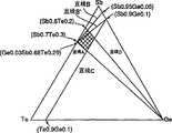
其特征在于,相变型记录层厚度为5nm以上25nm以下,由具有下述区域组成的GeSbTe合金为主要成分的薄膜构成,所述区域为在GeSbTe三元状态图中,用It is characterized in that the phase-change type recording layer has a thickness of not less than 5nm and not more than 25nm, and is composed of a thin film mainly composed of a GeSbTe alloy having the following region composition.
连接(Sb0.7Te0.3)与Ge的直线A、The straight line A connecting (Sb0.7 Te0.3 ) and Ge,
连接(Ge0.03Sb0.68Te0.29)与(Sb0.95Ge0.95)的直线B、Straight line B connecting (Ge0.03 Sb0.68 Te0.29 ) and (Sb0.95 Ge0.95 ),
连接(Sb0.9Ge0.1)与(Te0.9Ge0.1)的直线C、以及A straight line C connecting (Sb0.9 Ge0.1 ) and (Te0.9 Ge0.1 ), and
连接(Sb0.8Te0.2)与Ge的直线D等4条直线包围的区域(但不包含边界线上),The area surrounded by 4 straight lines (but not including the boundary line) such as the straight line D connecting (Sb0.8 Te0.2 ) and Ge,
第2保护层膜厚为5nm以上30nm以下。The film thickness of the second protective layer is not less than 5 nm and not more than 30 nm.
本发明的另一要点是适于与上述媒体一起使用的理想的光记录方法。Another gist of the present invention is an ideal optical recording method suitable for use with the above-mentioned media.
附图概述Figure overview
图1所示为非晶态斑点形状之一例。Figure 1 shows an example of an amorphous spot shape.
图2所示为在本发明媒体之一例进行记录时的反射率变化图。Fig. 2 is a graph showing changes in reflectance when recording is performed on an example of the medium of the present invention.
图3为表示本发明媒体的记录层的组成范围的GeSbTe三元状态图。Fig. 3 is a GeSbTe ternary state diagram showing the composition range of the recording layer of the medium of the present invention.
图4为表示已有的GeSbTe组成范围的GeSbTe三元状态图。Fig. 4 is a GeSbTe ternary state diagram showing the composition range of the conventional GeSbTe.
图5为表示本发明媒体的层结构之一例的示意图。Fig. 5 is a schematic diagram showing an example of the layer structure of the medium of the present invention.
图6为表示信号强度与信号振幅及调制度的关系用的信号波形图。Fig. 6 is a signal waveform diagram showing the relationship between signal strength, signal amplitude and modulation degree.
图7为说明反射率与第1保护层膜厚的依从关系的曲线图。Fig. 7 is a graph illustrating the dependence of the reflectance on the film thickness of the first protective layer.
图8所示为功率3值调制记录方式的脉冲分割方法之一例。Fig. 8 shows an example of a pulse division method in the power ternary modulation recording method.
图9为说明记录层温度随时间变化的示意图。Fig. 9 is a schematic diagram illustrating changes in temperature of a recording layer with time.
图10所示为适于斑点长度调制记录的功率3值调记录方式的脉冲分割方法之一例。FIG. 10 shows an example of a pulse division method in a power 3-level modulation recording method suitable for spot length modulation recording.
图11为说明实现图10的脉冲分割方法用的3种门信号发生电路时序的概念图。FIG. 11 is a conceptual diagram illustrating timings of three kinds of gate signal generating circuits for realizing the pulse division method of FIG. 10 .
图12所示为实施例1与比较例1中跳动与重放光功率的依从关系曲线图。FIG. 12 is a graph showing the dependence relationship between jitter and playback optical power in
图13所示为实施例1中跳动与记录脉冲分割方法的依从关系的曲线图。FIG. 13 is a graph showing the dependence relationship between jitter and recording pulse division method in
图14所示为实施例1中跳动与记录脉冲分割方法的依从关系的曲线图。FIG. 14 is a graph showing the dependence relationship between jitter and recording pulse division method in
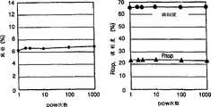
图15所示为实施例2中跳动、反射率及调制度与记录功率的依从关系的曲线图。FIG. 15 is a graph showing the dependence of jitter, reflectivity and modulation on recording power in Example 2. FIG.
图16所示为实施例2中跳动、反射率及调制度与反复重写次数的依从关系的曲线图。FIG. 16 is a graph showing the dependence of jitter, reflectivity, and modulation on the number of repeated rewriting times in
图17所示为实施例2(g1)与实施例2(d2)中跳动与斑点长度的依从关系的曲线图。Fig. 17 is a graph showing the dependence of jitter and spot length in Example 2 (g1) and Example 2 (d2).
图18所示为实施例2中跳动与基板倾角的依从关系的曲线图。FIG. 18 is a graph showing the dependence of runout and substrate inclination in Example 2. FIG.
图19所示为实施例4中10次重写后的跳动与αl及αc的依从关系的曲线图。FIG. 19 is a graph showing the dependence of jitter on αl and αc after 10 overwrites in
图20所示为实施例4中跳动、Rtop及调制度与反复重写次数的依从关系的曲线图。FIG. 20 is a graph showing the dependence of jitter, Rtop, and modulation on the number of repeated rewriting times in
图21(a)所示为实施例6中跳动与脉冲分割方法的依从关系的曲线图,图21(b)所示为实施例6中跳动与写入功率的依从关系的曲线图,图21(c)为实施例6中10次重写后的Rtop及调制度与写入功率的依从关系的曲线图。Figure 21 (a) is a graph showing the dependence of jitter and the pulse division method in
图22所示为实施例6中跳动、Rtop及调制度与反复重写次数的依从关系的曲线图。FIG. 22 is a graph showing the dependence of jitter, Rtop, and modulation on the number of repeated rewriting times in
图23所示为实施例6中跳动与斑点长度的依从关系的曲线图。FIG. 23 is a graph showing the dependence of jitter and spot length in Example 6. FIG.
图24(a)所示为比较例2中跳动与脉冲分割方法的依从关系的曲线图,图24(b)所示为比较例2中跳动与写入功率的依从关系的曲线图,图24(c)所示为10次重写后的Rtop及调制度与写入功率的依从关系的曲线图。Figure 24 (a) is a graph showing the dependence of jitter and pulse division method in Comparative Example 2, and Figure 24 (b) is a graph showing the dependence of jitter and write power in Comparative Example 2, Figure 24 (c) is a graph showing the Rtop after 10 overwrites and the dependence of the modulation degree on the write power.
图25表示为比较例3所用的记录方法的脉冲分割方法。FIG. 25 shows a pulse division method for the recording method used in Comparative Example 3. In FIG.
图26所示为比较例3中跳动与斑点长度及线速度的依从关系的曲线图。FIG. 26 is a graph showing the dependence of jitter on spot length and linear velocity in Comparative Example 3. FIG.
图27所示为比较例6中跳动与Pw及Pe的依从关系的曲线图。FIG. 27 is a graph showing the dependence of jitter on Pw and Pe in Comparative Example 6. FIG.
图28所示为实施例8中跳动与最短斑点长度的依从关系的曲线图。FIG. 28 is a graph showing the dependence of jitter and the shortest spot length in Example 8. FIG.
图29所示为实施例10及比较例8中跳动与Pw的依从的曲线图。FIG. 29 is a graph showing the dependence of jitter and Pw in Example 10 and Comparative Example 8. FIG.
图30为数字数据信号与摆动波形关系的说明图。Fig. 30 is an explanatory diagram of the relationship between a digital data signal and a wobble waveform.
图31为利用数字数据信号调制摆动(wobblc)波形的原理说明图。Fig. 31 is an explanatory diagram of the principle of modulating a wobble (wobblc) waveform with a digital data signal.
图32为实施例11中调制度与Rtop的槽宽的依从关系的曲线图。FIG. 32 is a graph showing the dependence of the degree of modulation on the groove width of Rtop in
发明的详细说明Detailed Description of the Invention
本发明者发现,在将晶态作为未记录及擦除状态、将非晶态作为记录状态的相变型媒体中,利用从非晶态部分或熔融部分与周围结晶态部分的边界开始的晶体生长实际上进行的再结晶化来进行擦除的媒体能够进行高速且高密度、稳定的记录。也就是说,能够进行高速重写,能够进行斑点边界的跳动小的,高密度的斑点长度调制记录,形成的斑点具有非常好的长期稳定性。The inventors of the present invention have found that in a phase-change medium in which the crystalline state is the unrecorded and erased state and the amorphous state is the recorded state, the use of crystals starting from the boundary between the amorphous portion or the molten portion and the surrounding crystalline portion A medium that is erased by growing recrystallization that actually proceeds can perform high-speed, high-density, and stable recording. That is to say, high-speed rewriting is possible, high-density spot length modulation recording with small spot boundary jitter is possible, and the formed spots have very good long-term stability.
通常,非晶态斑点的擦除过程,是将记录层加热至结晶化温度以上稍低于熔点的温度,形成非晶固态或熔融状态,然后在冷却时进行再结晶化而完成的。Usually, the erasing process of amorphous spots is completed by heating the recording layer to a temperature above the crystallization temperature and slightly lower than the melting point to form an amorphous solid or molten state, and then recrystallize when cooling.
本发明者的研究表明,非晶态斑点的擦除即再结晶化虽然是通过①非晶态区域内的晶核生成、②以非晶态部分或熔融部分与结晶态部分的边界为起点进行晶体生长这两个过程进行的,但实际上前者的晶核生成几乎不发生,而仅利用后者的晶体生长过程,能够得到上述效果。Research by the present inventors has shown that erasure of amorphous spots, that is, recrystallization, occurs through (1) nucleation in the amorphous region and (2) starting from the boundary between the amorphous part or the molten part and the crystalline part. These two processes of crystal growth are carried out, but in fact, the former crystal nucleation hardly occurs, and the above-mentioned effect can be obtained only by using the latter crystal growth process.
通常,结晶化是在结晶温度以上稍低于熔点的温度下进行的,晶核生成是在该温度范围内较低温度的一侧进行,而晶体生长是在其高温侧进行。不能说没有晶核生成就不能擦除,若以与围绕非晶态部分或熔融部分的周围结晶态区域的边界点作为晶核高速进行晶体生长,则能够擦除。Usually, crystallization is carried out at a temperature slightly lower than the melting point above the crystallization temperature, crystal nucleation is carried out on the lower temperature side of the temperature range, and crystal growth is carried out on the high temperature side. It cannot be said that erasing is impossible without formation of crystal nuclei, but erasing can be achieved by growing crystals at high speed using the boundary points with the surrounding crystalline regions surrounding the amorphous portion or the molten portion as crystal nuclei.
特别是越是微小的斑点或短的斑点,仅仅利用从这样的周围晶态部分开始的晶体生长,很容易在瞬时间结晶直到斑点中心,因此能够在极短的时间内完全擦除。因而唯有采用最短斑点长度为0.5μm以下的微小斑点的高密度记录媒体,效果才显著,能够在100纳秒数量级以下擦除,能够进行高速重写。In particular, the finer spots or short spots can be easily crystallized to the center of the spots in an instant only by crystal growth from such peripheral crystalline parts, and thus can be completely erased in an extremely short time. Therefore, only a high-density recording medium with tiny spots with a shortest spot length of 0.5 μm or less can achieve significant effects. It can be erased under the order of 100 nanoseconds and can be rewritten at a high speed.
而且通常是,最短斑点长度越短越能够进行高密度记录,但从斑点的稳定性来看,最好在10nm以上。In general, the shorter the shortest spot length is, the more high-density recording can be performed. However, from the viewpoint of spot stability, it is preferably 10 nm or more.
另外,斑点的横向宽度越窄,仅仅利用从周围晶态部分开始晶体生长,越容易瞬时间结晶到斑点中心,这是所希望的。因而此最好是记录信息的道的道间距例如取0.8μm以下,斑点横向宽度不要太宽。通常,斑点横向宽度为道间距的一半左右。通常道间距越窄,越能够进行高密度记录,但从斑点稳定性来看,最好在0.1μm以上。道也可以仅仅是槽沟,也可以是槽沟与槽脊两者。In addition, the narrower the lateral width of the spot, the easier it is to instantaneously crystallize to the center of the spot by only starting crystal growth from the surrounding crystalline portion, which is desirable. Therefore, it is preferable that the track pitch of the track for recording information is, for example, 0.8 μm or less, and the lateral width of the spot should not be too wide. Typically, the spot lateral width is about half the track pitch. Generally, the narrower the track pitch, the more capable of high-density recording, but from the viewpoint of spot stability, it is preferably 0.1 μm or more. The track may also be only a groove, or both grooves and lands.
本发明的媒体还具有非常好的非晶态斑点的长期稳定性。The media of the present invention also have very good long-term stability of amorphous spots.
也就是说,从周围结晶态部分开始的晶体生长,即使是在结晶温度以上稍低于熔点的范围内,也仅仅在接近熔点的较高温区域进行,在低温几乎不进行,因此一旦形成非晶态斑点,就难以结晶,有很好的长期稳定性,结晶温度通常在100℃~200℃范围内,在到达该温度左右之前,能够维持热稳定性。That is to say, the crystal growth from the surrounding crystalline part, even in the range above the crystallization temperature and slightly below the melting point, only proceeds in the higher temperature region close to the melting point, and hardly proceeds at low temperatures, so once the amorphous If there are no state spots, it is difficult to crystallize, and it has good long-term stability. The crystallization temperature is usually in the range of 100 ° C to 200 ° C, and it can maintain thermal stability before reaching this temperature.
特别是在不到100℃的通常的使用范围内,记录的非晶态斑点极其稳定,记录下来的信号振幅几乎不劣化。反之也可以从那样的长期稳定性得出几乎不伴随着生成晶核的结论。In particular, the recorded amorphous spots are extremely stable in the usual operating range of less than 100°C, and the amplitude of the recorded signal hardly deteriorates. Conversely, it can be concluded from such long-term stability that crystal nucleation hardly occurs.
再者,本发明媒体的优点在于,在斑点长度记录中,能够形成起伏极少的光滑的斑点边界。Furthermore, the medium of the present invention is advantageous in that, in spot length recording, a smooth spot boundary with very little waviness can be formed.
通常在记录非晶态斑点时,是使记录层暂时熔融再凝固而形成非晶态,由于斑点边缘部分比中心温度低,因此,向来在斑点边缘部分容易因晶核生长导致再结晶,产生非晶态混入的粗大晶粒,这成为斑点边界起伏的原因。Generally, when recording amorphous spots, the recording layer is temporarily melted and then solidified to form an amorphous state. Since the edge of the spot is at a lower temperature than the center, it has always been easy to recrystallize due to nuclei growth at the edge of the spot, resulting in amorphous Coarse crystal grains mixed in the crystalline state, which become the cause of spot boundary fluctuations.
本发明媒体的特征在于,擦除时,从非晶态部分或熔融部分与结晶态部分的边界开始的晶体生长是起支配作用的,而且高速进行的,这种情况下记录时虽然也是同样原理起作用,但在熔融区域再凝固并非晶化时,也仅仅发生从周围结晶态部分开始的晶体生长,因晶核生长而引起的结晶化不容易发生,斑点边界不易起伏。The medium of the present invention is characterized in that during erasing, the crystal growth from the boundary between the amorphous part or the molten part and the crystalline part plays a dominant role, and it is carried out at a high speed. In this case, the same principle is also applied during recording. It works, but when the molten region is resolidified and not crystallized, only crystal growth from the surrounding crystalline part occurs, crystallization due to crystal nucleus growth does not easily occur, and the spot boundary is not easy to fluctuate.
也就是说,从周围结晶态部分开始的晶体生长,即使是在结晶温度以上稍低于熔点的范围内,也仅仅在接近熔点的较高温区域进行,在较低温几乎不进行,因此从熔融状态再凝固时,仅仅根据温度下降通过熔点时的冷却速度来决定非晶态斑点的边界形状。That is to say, the crystal growth from the surrounding crystalline state, even in the range above the crystallization temperature and slightly below the melting point, only proceeds in the higher temperature region close to the melting point, and hardly proceeds at lower temperatures, so from the molten state During resolidification, the boundary shape of the amorphous spots is determined solely by the cooling rate as the temperature drops through the melting point.
因而,以往存在的问题即再凝固时发生的因晶核生长而产生的混有非晶态的粗大晶粒,在非晶态斑点周围几乎完全不形成。显然这对于抑制因斑点边界起伏而产生的噪声是极其有效的。Therefore, coarse crystal grains mixed with amorphous state generated by nuclei growth during resolidification, which has been a conventional problem, are hardly formed around amorphous spots. Apparently this is extremely effective in suppressing noise caused by spot boundary fluctuations.
另外,斑点边界形状也很稳定,不会随时间而变化,因此不仅开始时的跳动小,而且跳动也几乎不随时间而劣化。Also, the spot boundary shape is stable and does not change over time, so not only is the jitter at the beginning small, but the jitter hardly deteriorates over time.
下面更详细说明本发明的结晶化原理。The crystallization principle of the present invention will be described in more detail below.
在本媒体中,非晶态斑点与周围结晶态部分的边界部份是晶体生长核,在非晶态斑点内部几乎不产生晶核。因而,仅仅从斑点边界部分开始晶体生长。In this medium, the boundary portion between the amorphous spot and the surrounding crystalline part is a crystal growth nucleus, and almost no crystal nuclei are generated inside the amorphous spot. Thus, crystal growth starts only from the spot boundary portion.
而已有的GeTe-Sb2Te3系记录层,在非晶态斑点内随机生成晶核,该晶核生长进而结晶化。On the other hand, in the conventional GeTe-Sb2 Te3 -based recording layer, crystal nuclei are randomly generated in amorphous spots, and the crystal nuclei grow and crystallize.
两者结晶化过程的差别可以用透射电子显微镜加以验证。若对非晶态斑点形成后的两记录层恒定照射较低功率的擦除光,则可以观察到GeTe-Sb2Te3系记录层从温度高的非晶态斑点中央部分开始结晶化,而与此不同的是,在本发明记录层中可以观察到从非晶态斑点周围部分开始晶体生长。特别是从非晶态斑点的前端及后端开始的晶体生长很明显。The difference between the two crystallization processes can be verified by transmission electron microscopy. If the two recording layers after the formation of the amorphous spot are constantly irradiated with low-power erasing light, it can be observed that the GeTe-Sb2 Te3 system recording layer begins to crystallize from the central part of the amorphous spot at a high temperature, while In contrast to this, in the recording layer of the present invention, crystal growth was observed from the portion around the amorphous spot. In particular, crystal growth from the front and rear ends of the amorphous spot is evident.
根据这样的原理进行擦除的记录层组成多为在Sb0.7Te0.3共晶点邻近组成中添加过剩的Sb及最多20原子%左右的其他元素构成的合金系。亦即以My(SbxTe1-x)1-y合金为主要成分的薄膜(式中0.6≤X≤0.9,0<y≤0.2,M为Ga、Zn、Ge、Sn、Si、Cu、Au、Al、Pd、Pt、Pd、Cr、Co、O、S、Se、Ta、Nb及V中的至少一种)。The composition of the recording layer to be erased based on this principle is often an alloy system in which an excess of Sb and up to 20 atomic % of other elements are added to the composition near the Sb0.7 Te0.3 eutectic point. That is, a thin film mainly composed ofMy (Sbx Te1-x )1-y alloy (where 0.6≤X≤0.9, 0<y≤0.2, M is Ga, Zn, Ge, Sn, Si, Cu , Au, Al, Pd, Pt, Pd, Cr, Co, O, S, Se, Ta, Nb and V at least one).
Sb0.7Te0.3中含有过剩Sb的合金,具有如下特征,即与GeTe-Sb2Te3伪二元合金系相比,其从非晶态斑点周围部分的晶体开始的晶体生长明显大,因此能够以高线速度进行重写。过剩的Sb不会促进非晶态斑点内的随机的晶核生成及晶核生长,而是大幅度增加从周围结晶态部分开始的晶体生长速度。The alloy containing excess Sb in Sb0.7 Te0.3 has a feature that the crystal growth from the crystal around the amorphous spot is significantly larger than the GeTe-Sb2 Te3 pseudo-binary alloy system, so it can Rewrite at high line speed. Excess Sb does not promote random nucleation and nuclei growth in the amorphous spot, but greatly increases the crystal growth rate from the surrounding crystalline portion.
但是,在SbTe二元合金中,也生成很多晶核,因此非晶态斑点的长期稳定性极差,必须添加适当的元素。However, in the SbTe binary alloy, many crystal nuclei are also generated, so the long-term stability of amorphous spots is extremely poor, and appropriate elements must be added.
根据本发明者的研究,添加Ge对于抑制晶核生成是极具有效的。According to the studies of the present inventors, the addition of Ge is extremely effective in suppressing the generation of crystal nuclei.
再者,非晶态斑点的再结晶实际上是否仅仅由从周围结晶态部分开始的再结晶起支配作用,可以根据长期稳定性的评价间接了解。Furthermore, whether the recrystallization of amorphous spots is actually dominated only by recrystallization from surrounding crystalline parts can be indirectly learned from the evaluation of long-term stability.
作为具体的评价方法,有下面所述的方法,即进行高温高湿下的加速环境试验时测量重放信号的调制度的方法。As a specific evaluation method, there is the following method of measuring the degree of modulation of a reproduced signal when performing an accelerated environmental test under high temperature and high humidity.
也就是说,在利用最短斑点长度为0.5μm以下的多种斑点长度记录信号时,以M0表示刚记录下即重放的信号的调制度,That is to say, when recording signals with various spot lengths whose shortest spot length is 0.5 μm or less,M0 represents the modulation degree of the signal that is just recorded and reproduced,
记录后在80℃ 80%RH条件下经过1000小时后重放的信号的调制度记为M1,则满足如下关系,即The modulation degree of the signal replayed after 1000 hours at 80°C and 80% RH after recording is denoted as M1 , which satisfies the following relationship, namely
M1/M0≥0.9M1 /M0 ≥0.9
斑点长度调制方式没有限定,可以使用EFM调制、EFM增强型调制、(1,7)RLL-NRZI(run length limited-non return to zero inverted,即有限游程长度码-IBM式不归零编码)调制等。以最短斑点长度为0.5μm以下将如图6所示的随机信号加以记录,在进行本评价时,最好最短斑点长度为0.2μm左右以上。另外,不必要在全部评价条件中不必满足上式,只要在一个评价条件中满足上式即可。The spot length modulation method is not limited, and EFM modulation, EFM enhanced modulation, (1,7) RLL-NRZI (run length limited-non return to zero inverted, limited run length code-IBM non-return to zero coding) modulation can be used wait. Random signals as shown in FIG. 6 were recorded with the shortest spot length being 0.5 μm or less. In this evaluation, the shortest spot length is preferably about 0.2 μm or more. In addition, it is not necessary to satisfy the above formula in all the evaluation conditions, and it is only necessary to satisfy the above formula in one of the evaluation conditions.
例如利用最短斑点长度0.4μm的多种斑点长度记录EFM增强型调制方式的随机信号。For example, a random signal of the EFM enhanced modulation method is recorded using various spot lengths with the shortest spot length of 0.4 μm.
调制度是用最大信号强度对该调制方式的最长的斑点的信号振幅进行归一化的值。图6所示为将EFM增强型调制的随机信号录放时的DC重放信号(含有直流分量的重放信号)波形。调制度以14T斑点的最大信号强度Itop与信号振幅I14之比I14/Itop来定义。The degree of modulation is a value obtained by normalizing the signal amplitude of the longest spot of the modulation scheme with the maximum signal strength. Figure 6 shows the waveform of the DC replay signal (replay signal containing a DC component) when the EFM enhanced modulated random signal is recorded and played back. The degree of modulation is defined by the ratio I14/Itop of the maximum signal intensity Itop of the 14T spot to the signal amplitude I14.
若调制度不变,则可以认为非晶态斑点尺寸非常稳定。若加速试验前记录的随机信号的调制度在加速试验后也保持初始值的90%以上,则能够推断实际上没有同时伴随生成晶核。If the degree of modulation does not change, it can be considered that the size of the amorphous spot is very stable. If the degree of modulation of the random signal recorded before the accelerated test remained at 90% or more of the initial value even after the accelerated test, it can be inferred that crystal nuclei were not actually concomitantly generated.
在本发明的记录层中,由于从周围结晶态部分开始的晶体生长容易在略低于熔点的高温区域发生,因此在为了形成非晶态斑点而使记录层熔化、再凝固时,也能够从周围的结晶态部分开始发生晶体生长。因而,在熔融后冷却速度慢,未能达到作为非晶态固化所需要的临界冷却速度时,整个熔融区域几乎在瞬间再结晶。In the recording layer of the present invention, since the crystal growth from the peripheral crystalline part tends to occur in a high-temperature region slightly lower than the melting point, when the recording layer is melted and resolidified in order to form amorphous spots, it can also be formed from Crystal growth begins to occur in the surrounding crystalline portion. Therefore, when the cooling rate is slow after melting and the critical cooling rate required for solidification as an amorphous state cannot be reached, the entire molten region recrystallizes almost instantly.
这可以通过以下实验加以确认。This can be confirmed by the following experiment.
在设有引导录放光束的槽的0.6mm厚的聚碳酸酯基板上,依次设置膜厚68nm的(ZnS)80(SiO2)20的第1者保护层、膜厚18nm的Ge0.05Sb0.71Te0.24记录层、膜厚20nm的(ZnS)80(SiO2)20的第2保护层及膜厚250nm的Al0.995Ta0.005的反射层,再设置膜厚4μm的紫外线硬化树脂保护层。将两片这样基板的有记录层一侧作为内侧,用光熔粘接剂粘贴,构成光记录媒体。本记录层组成为应该能够以约7m/s以上的线速度重写的Sb/Te≈3。将长轴约100μm、短轴约1.5μm的椭圆激光在短轴方向对本媒体进行扫描,使其熔融、再结晶,实现初始化。On a polycarbonate substrate with a thickness of 0.6mm provided with grooves for guiding recording and reproducing beams, a first protective layer of (ZnS)80 (SiO2 )20 with a film thickness of 68nm and Ge0.05 Sb0.71 Te with a film thickness of 18nm were sequentially provided0.24 recording layer, 20nm thick (ZnS)80 (SiO2 )20 second protective layer, 250nm thick Al0.995 Ta0.005 reflective layer, and 4μm thick ultraviolet curing resin protective layer. An optical recording medium is constituted by adhering two such substrates with the recording layer side as the inner side with an optical melt adhesive. The present recording layer composition is Sb/Te≈3, which should allow rewriting at a linear velocity of about 7 m/s or higher. Scan the medium with an elliptical laser with a long axis of about 100 μm and a short axis of about 1.5 μm in the direction of the short axis to melt, recrystallize, and initialize.
将波长637nm、NA=0.63的聚焦光束沿导向槽以7m/s的线速度照射在本媒体上。在将记录功率Pw为10mW的记录光恒定照射后,急剧减少功率到1mW。亦即实际上切断记录光。另外,光束直径约0.9μm,相当于高斯光束中的能量强度为峰值强度的1/e2以上的区域。A focused beam with a wavelength of 637nm and NA=0.63 is irradiated on the medium at a linear velocity of 7m/s along the guide groove. After constant irradiation of recording light with a recording power Pw of 10 mW, the power was sharply reduced to 1 mW. That is, the recording light is actually cut off. In addition, the beam diameter is about 0.9 μm, which corresponds to a region where the energy intensity of a Gaussian beam is 1/e2 or more of the peak intensity.
图2所示为切断记录光前后的反射率变化。如图2的下图所示,经过一段时间切断记录光。在图2下图的左侧,记录光是连续的,即恒定照射,在右侧记录光被切断。用重放功率为1.0mW的重放光对同一区域进行扫描,则得到图2上图所示的重放波形。这对应于反射率变化。FIG. 2 shows changes in reflectance before and after cutting off the recording light. As shown in the lower diagram of Fig. 2, the recording light is cut off after a certain period of time. On the left side of the lower diagram in Figure 2, the recording light is continuous, ie, constantly illuminated, and on the right side the recording light is cut off. Scan the same area with playback light with a playback power of 1.0mW, and the playback waveform shown in the upper figure of Figure 2 is obtained. This corresponds to a change in reflectivity.
在瞬间切断记录光的附近,反射率下降,而在其前后,则反射率基本相同,根据TEM观察确认,反射率下降部分为非晶态,在其前后为晶态。也就是说,只要连续照射记录光,熔融部分就再结晶,而仅仅在切断记录光部分附近的熔融区域发生非晶化。The reflectance decreases in the vicinity of instantaneous cutoff of the recording light, and the reflectance before and after it is substantially the same. According to TEM observation, it was confirmed that the portion where the reflectance decreased was amorphous, and before and after it was crystalline. That is, as long as the recording light is continuously irradiated, the melted portion is recrystallized, and only the melted portion near the portion where the recording light is cut off becomes amorphized.
这是因为,连续照射记录光时,利用后续部分来的余热,抑制了记录层的冷却速度,不能得到形成非晶态所必需的临界冷却速度,而反之,一旦切断记录光,也就切断后续部分来的余热,就能够提高冷却速度。This is because when recording light is irradiated continuously, the cooling rate of the recording layer is suppressed by the waste heat from the subsequent part, and the critical cooling rate necessary for the formation of an amorphous state cannot be obtained. On the contrary, once the recording light is cut off, the subsequent part is also cut off. Part of the waste heat can increase the cooling rate.
另外,将记录功率Pw设为7mW以上时,利用切断记录光,就能够形成非晶态斑点。In addition, when the recording power Pw is set to 7 mW or more, amorphous spots can be formed by cutting off the recording light.
由研究的结果可知,本发明媒体以一定线速度连续照射足以使记录层熔融的记录功率Pw的记录光,则大致再结晶化,再以一定线速度在足以使记录层熔融的记录功率Pw的记录光之后照射功率近似为0的记录光,即形成非晶态斑点。所谓功率近似为0,没有必要严格为0,是取满足0≤Pb≤0.2Pw的偏置功率Pb,最好是0≤Pb≤0.1Pw的偏置功率Pb。As can be seen from the results of the research, the medium of the present invention is substantially recrystallized by continuously irradiating the recording light of the recording power Pw sufficient to melt the recording layer at a certain linear velocity, and then at a constant linear velocity at a recording power Pw sufficient to melt the recording layer. After the recording light is irradiated with recording light whose power is approximately 0, amorphous spots are formed. The so-called power is approximately 0, not necessarily strictly 0, but the bias power Pb satisfying 0≤Pb≤0.2Pw, preferably 0≤Pb≤0.1Pw.
在本发明中,熔融部分再凝固时的再结晶化几乎都是仅仅由于从周围固相晶态部分开始的晶体生长而引起的。因而,再结晶部分不是在非晶态斑点的中心部分形成,所以能够形成光滑连续的斑点边界。In the present invention, the recrystallization at the time of resolidification of the molten portion is almost all due to crystal growth from the surrounding solid-phase crystalline portion. Therefore, the recrystallized portion is not formed at the central portion of the amorphous spot, so smooth and continuous spot boundaries can be formed.
以往一直认为,这样明显容易再晶化的材料不适合斑点长度记录用的记录层。这是因为,若为了形成长斑点而长时间照射记录光,则熔融区域几乎都结晶化了。Conventionally, it has been considered that such a material that is significantly easily recrystallized is not suitable for a recording layer for spot length recording. This is because when the recording light is irradiated for a long time to form long spots, almost all of the melted regions are crystallized.
但是,根据本发明者的研究,在最短斑点长度为0.5μm以下的高密度记录中,将熔融区域的非晶化与从周围固相结晶态部分的边界开始的再结晶化的竞争过程积极加以利用,更能够得到良好的跳动。However, according to the research of the present inventors, in high-density recording with a shortest spot length of 0.5 μm or less, the competitive process of amorphization of the molten region and recrystallization from the boundary of the surrounding solid-phase crystalline portion is actively suppressed. Using it, you can get a better beating.
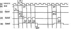
因此发现,在如下所述长度nT的斑点形成中,将记录功率Pw施加区间与其切断区间、即偏置功率Pb施加区间加以组合的脉冲分割方式是极其有效的。Therefore, it has been found that the pulse division method in which the recording power Pw application period is combined with the bias power Pb application period, that is, the bias power Pb application period, is extremely effective in forming a spot with a length nT as described below.
若利用脉冲分割方式进行记录,则如图1所示,形成箭羽型(或月牙型)非晶态部分相连的非晶态斑点。If the pulse division method is used for recording, as shown in FIG. 1 , an arrow-feather-shaped (or crescent-shaped) amorphous spot is formed in which the amorphous parts are connected.
该斑点前端形状仅仅由最前面的箭羽型非晶态部分的前端的形状决定,而该斑点后端形状仅仅由最后面的箭羽型非晶态部分的后端的形状决定。The shape of the front end of the speckle is determined only by the shape of the front end of the foremost fringe-type amorphous portion, and the shape of the rear end of the speckle is determined only by the shape of the rear end of the rearmost fletch-type amorphous portion.
通常,由于非晶态部分的前端形状是光滑的,因此斑点前端形状也是光滑的。这是由于向前方的散热,冷却速度保持足够快,因而大致反映熔融区域前端的形状,所以由记录脉冲上升沿时间来决定。记录脉冲、即Pw施加区间的上升沿只要是2~3纳秒以下即可。Usually, since the shape of the tip of the amorphous part is smooth, the shape of the tip of the spot is also smooth. This is due to the heat dissipation to the front, and the cooling rate is kept fast enough, thus roughly reflecting the shape of the front end of the melting region, so it is determined by the rising edge time of the recording pulse. The recording pulse, that is, the rising edge of the Pw application period may be 2 to 3 nanoseconds or less.
而非晶态部分的后端形状是由记录脉冲下降沿时间决定的冷却速度及从周围、特别是后端晶态部分开始进行的再结晶区域的大小来决定的。为了使冷却速度足够快,Pw施加区间的下降沿最好是2~3纳秒以下。再结晶区域大小可以利用脉冲切断区间、即Pb施加区间的长度来正确控制。The shape of the rear end of the amorphous part is determined by the cooling rate determined by the falling edge time of the recording pulse and the size of the recrystallized region starting from the surrounding, especially the rear crystalline part. In order to make the cooling rate sufficiently fast, the falling edge of the Pw application period is preferably 2 to 3 nanoseconds or less. The size of the recrystallized region can be precisely controlled by the length of the pulse cut-off interval, that is, the Pb application interval.
还有一点也很重要,即采用上述超急冷构造作为层结构,尽可能使记录层冷却速度急剧变化,同时在斑点后端附近使冷却速度的空间分布陡峭,以使得斑点端部位置不起伏。It is also important to use the above-mentioned super-quenching structure as the layer structure to change the cooling rate of the recording layer as rapidly as possible, and at the same time make the spatial distribution of the cooling rate steep near the rear end of the spot so that the position of the end of the spot does not fluctuate.
本发明者根据对能够高速记录短斑点、且记录斑点的长期稳定性优异的光记录媒体专心研究的结果发现,在Sb0.7Te0.3共晶组成附近添加Ge的特定组成特别优异,同时通过适当选择层结构,得到了其他特性也优异的光记录媒体。As a result of intensive research on an optical recording medium capable of recording short spots at high speed and having excellent long-term stability of recorded spots, the present inventors have found that a specific composition in which Ge is added near the eutectic composition of Sb0.7 Te0.3 is particularly excellent. layer structure, an optical recording medium excellent in other characteristics was obtained.
也就是说,注意研究了对Sb0.7Te0.3添加过剩的Sb及Ge而得到的以往没有的三元合金,讨论了对高密度斑点长度调制记录的适应性。结果发现,在图3所示的GeSbTe三元状态图中,若采用4条直线A、B、C、D包围的极其有限的Ge-Sb-Te比的记录层组成,以此构成的媒体在高密度斑点长度调制记录中,其反复重写耐久性及长期稳定性特别优异。That is, attention was paid to studying a ternary alloy obtained by adding excess Sb and Ge to Sb0.7 Te0.3 , which was not available before, and the suitability for high-density spot length modulation recording was discussed. It was found that, in the GeSbTe ternary state diagram shown in Figure 3, if a recording layer composition with an extremely limited Ge-Sb-Te ratio surrounded by four straight lines A, B, C, and D is used, the medium formed by this will In high-density spot length modulation recording, it is particularly excellent in repeated rewriting durability and long-term stability.
也就是说,将在GeSbTe三元状态图中,That is, in the GeSbTe ternary state diagram,
具有用useful
连接(Sb0.7Te0.3)与Ge的直线A、The straight line A connecting (Sb0.7 Te0.3 ) and Ge,
连接(Ge0.03Sb0.68Te0.29)与(Sb0.95Ge0.05)的直线B、Straight line B connecting (Ge0.03 Sb0.68 Te0.29 ) and (Sb0.95 Ge0.05 ),
连接(Sb0.9Ge0.1)与(Te0.9Ge0.1)的直线C、以及A straight line C connecting (Sb0.9 Ge0.1 ) and (Te0.9 Ge0.1 ), and
连接(Sb0.8Te0.2)与Ge的直线D等4条直线包围的区域(但不包含边界线上)的组成的GeSbTe合金为主要成分的薄膜作为记录层。对该记录层通过采用后述的层结构,构成非常适于最短斑点长度为0.5μm以下的高密度斑点长度调制记录的媒体。而且,能够得到与DVD相同的记录密度及与DVD之间的优异的重放互换性。A thin film composed mainly of GeSbTe alloy in the region surrounded by four straight lines (but not including the boundary line) connecting (Sb0.8 Te0.2 ) and Ge straight line D was used as a recording layer. By adopting the layer structure described below for this recording layer, a medium suitable for high-density spot length modulation recording with a shortest spot length of 0.5 μm or less is constituted. Furthermore, it is possible to obtain the same recording density as DVD and excellent playback compatibility with DVD.
而且对于反复重写耐久性及记录功率和擦除功率的变动,还能够确保得到较小跳动所需的足够余量。In addition, it is possible to ensure a sufficient margin for obtaining a small jitter with respect to repeated rewriting durability and fluctuations in recording power and erasing power.
在该组成范围内,在SbyTe1-y合金中,Sb量越是比y=0.7的量多,则过剩的Sb量越是增加,结晶速度越快,能够实现高线速度的重写。Within this composition range, in the Sby Te1-y alloy, the more the Sb content is greater than the y=0.7 content, the more the excess Sb content increases, the faster the crystallization speed is, and high linear speed rewriting can be realized .
更具体来说,在EFM增强型调制记录(8-16调制的斑点长度调制记录)中,即使将最短斑点的3T斑点长度缩短至0.4μm或0.35μm,也能够得到较小的跳动。又能够得到足够的伺服信号,能够在已有的只读DVD驱动器中进行跟踪伺服。还能够在线速度为1~10m/s的任何线速度下进行重写。More specifically, in EFM enhanced modulation recording (spot length modulation recording of 8-16 modulation), even if the 3T spot length of the shortest spot is shortened to 0.4 μm or 0.35 μm, smaller jitter can be obtained. In addition, sufficient servo signals can be obtained to perform tracking servo in existing read-only DVD drives. It is also possible to perform rewriting at any linear velocity ranging from 1 to 10 m/s.
借助于此,能够得到与只读DVD相同容量、基本上具有重放互换性的可擦写DVD。With this, it is possible to obtain a rewritable DVD having the same capacity as a read-only DVD and basically having playback compatibility.
若控制过剩的Sb量,还能够以8m/s以上的高线速度实现上述高质量高密度的重写。另外,如下所述根据线速度改变记录脉冲分割方法(脉冲策略),能够在至少包含3~8m/s很宽的线速度范围内实现良好的重写。If the excess Sb amount is controlled, the above-mentioned high-quality and high-density rewriting can be realized at a high linear speed of 8 m/s or more. In addition, by changing the recording pulse division method (pulse strategy) according to the linear velocity as described below, good overwriting can be realized over a wide linear velocity range including at least 3 to 8 m/s.
下面详细说明本组成。This composition will be described in detail below.
在Ge添加量为10原子%以下的Sb0.7Te0.3共晶点邻近组成中,Sb/Te比越大,结晶速度有越是加快的趋势。这是由于与Sb0.7Te0.3相比是过剩的Sb在作为Sb原子团析出并在再结晶过程中作为晶核起作用。而与Sb0.7Te0.3相比没有过剩的Sb时,擦除性能差,实际上不能进行重写。另外,由于初始化时几乎没有核生成,因此还存在初始化困难、生产效率非常差的问题(直线A)。In the composition near the eutectic point of Sb0.7 Te0.3 in which the amount of Ge added is 10 atomic % or less, the crystallization rate tends to increase as the Sb/Te ratio increases. This is because Sb, which is excess compared to Sb0.7 Te0.3 , precipitates as Sb atomic groups and acts as crystal nuclei in the recrystallization process. On the other hand, when there is no excess Sb compared with Sb0.7 Te0.3 , the erasing performance is poor, and rewriting is practically impossible. In addition, since there is almost no kernel generation at the time of initialization, there is also a problem that initialization is difficult and production efficiency is very poor (line A).
另一方面,若在Sb0.7Te0.3共晶二元合金中增加Sb量,则结晶速度加快,而反之结晶温度也下降,损害了非晶态斑点的长期稳定性。又,不适合3m/s左右的低线速度的记录,形成的非晶态斑点用短时间的重放光(激光功率约1mW左右)照射即被擦除掉。因而,不应该包含比连接(Sb0.8Te0.2)与Ge的直线D更过剩的Sb。On the other hand, if the amount of Sb is increased in the Sb0.7 Te0.3 eutectic binary alloy, the crystallization rate will be accelerated, and conversely, the crystallization temperature will also decrease, which will damage the long-term stability of amorphous spots. Also, it is not suitable for recording at a low linear velocity of about 3m/s, and the formed amorphous spots are erased immediately after being irradiated with short-time playback light (laser power about 1mW). Therefore, Sb should not be contained in excess of the straight line D connecting (Sb0.8 Te0.2 ) andGe .
又,在用直线A与D规定的过剩Sb量的范围内,保持SbTe二元不变时,由于结晶温度低,而且存在过剩Sb的晶核,导致非晶态斑点过于不稳定,因此过剩Sb量越多,越添加Ge。利用Ge的4配位键,几乎完全抑制晶核生成。结果结晶温度上升,长期稳定性增加。连接(Ge0.03Sb0.68Te0.29)与(Sb0.95Ge0.05)的直线B规定了该条件。更理想的是比连接(Ge0.03Sb0.68Te0.29)与(Sb0.9Ge0.1)的直线B’含有更多的Ge。In addition, within the range of excess Sb specified by straight lines A and D, when the SbTe binary is kept unchanged, due to the low crystallization temperature and the presence of excess Sb nuclei, the amorphous spots are too unstable, so the excess Sb The more the amount, the more Ge is added. Utilizing the 4-coordinate bond of Ge, crystal nucleation is almost completely suppressed. As a result, the crystallization temperature increases and the long-term stability increases. The straight line B connecting (Ge0.03 Sb0.68 Te0.29 ) and (Sb0.95 Ge0.05 ) defines this condition. It is more desirable to contain more Ge than the straight line B' connecting (Ge0.03 Sb0.68 Te0.29 ) and (Sb0.9 Ge0.1 ).
再有,若Ge含量达到10原子%以上,则斑度长度记录时的跳动劣化,由于反复重写,高熔点的Ge化合物、特别是GeTe容易偏析。另外,由于刚成膜后的非晶态膜结晶化极其困难,这是不理想的(直线C)。为了减少跳动,最好取Ge为7.5原子%以下。Furthermore, when the Ge content is 10 atomic % or more, jitter during spot length recording deteriorates, and Ge compounds with a high melting point, especially GeTe, tend to segregate due to repeated overwriting. In addition, since crystallization of an amorphous film immediately after film formation is extremely difficult, this is not desirable (line C). In order to reduce jitter, Ge is preferably set at 7.5 atomic % or less.
另外,对于以线速度3m/s以上进行重写,记录层最好采用Gex(SbyTe1-y)1-x合金为主要成分的薄膜(0.04≤x<0.10、0.72≤y<0.8)。也就是说,对于线速度3m/s以上的记录,最好增加Sb量,在SbyTe1-y合金中,最好使y≥0.72。这里,由于增加Sb量,导致非晶态斑点稳定性有一些劣化,为了弥补这一点,最好使Ge多些,达到x≥0.04。In addition, for rewriting at a linear speed of 3m/s or more, the recording layer is preferably a thin film composed mainly of Gex (Sby Te1-y )1-x alloy (0.04≤x<0.10, 0.72≤y<0.8 ). In other words, for recording with a linear velocity of 3 m/s or more, it is better to increase the amount of Sb, and in the Sby Te1-y alloy, it is better to make y ≥ 0.72. Here, since the increase in the amount of Sb leads to some deterioration in the stability of the amorphous spots, in order to compensate for this, it is preferable to increase the amount of Ge so that x≥0.04.
再者,对于线速度7m/s以上的重写,记录层最好采用Gex(SbyTe1-y)1-x合金为主要成分的薄膜(0.045≤x≤0.075,0.74≤y<0.8)。也就是说,对于速度7m/s以上的记录,最好再多增加Sb量,在Sbye1-y合金中,最好使y≥0.74。这时,为了提高非晶态斑点的稳定性,使Ge量满足x≥0.045。另一方面,在高线速度下跳动容易劣化,为了弥补这一点,使Ge量满足x≤0.075。Furthermore, for rewriting with a linear velocity above 7m/s, the recording layer is preferably made of a film mainly composed of Gex (Sby Te1-y )1-x alloy (0.045≤x≤0.075, 0.74≤y<0.8 ). That is to say, for recordings with a speed of 7 m/s or more, it is better to increase the amount of Sb, and in the Sby e1-y alloy, it is better to make y ≥ 0.74. At this time, in order to improve the stability of the amorphous spots, the amount of Ge is made to satisfy x≧0.045. On the other hand, jitter tends to deteriorate at high linear speeds, and in order to compensate for this, the amount of Ge is made to satisfy x≤0.075.
至今已经有关于GeSbTe三元组成或以该三元组成为母体含添加元素的记录层组成的报告发表(日本专利特开昭61-258787号公报、特开昭62-53886号公报、特开昭62-152786号公报、特开平1-63195号公报、特开平1-211249号公报、特开平1-277338号公报)。So far, there have been reports on the GeSbTe ternary composition or the composition of the recording layer containing additional elements based on the ternary composition (Japanese Patent Laying-Open No. 61-258787, Japanese Patent Laid-Open No. 62-53886, Japanese Patent Laid-Open No. 62-53886, 62-152786, JP-A-1-63195, JP-1-211249, JP-1-277338).
但是,这些公报所述的组成都是Sb少于连接(Sb0.7Te0.3)与Ge的直线A的组成,与本发明组成范围不同。However, the compositions described in these publications are all compositions in which Sb is less than the straight line A connecting (Sb0.7 Te0.3 ) to Ge, which is different from the composition range of the present invention.
这些当然也是以Sb2Te3金属化合物组成为主体。另外,在GeTe-Sb2Te3伪二元合金系中,与本发明相反,由于过剩Sb具有减慢结晶速度的效果,因此在以5m/s以上高线速度进行重写时,在GeTe-Sb2Te3直线上,特别是使Ge2Sb2Te5组成含有过剩的Sb,当然是有害的。Of course, these are also mainly composed of Sb2 Te3 metal compounds. In addition, in the GeTe-Sb2 Te3 pseudo-binary alloy system, contrary to the present invention, since excess Sb has the effect of slowing down the crystallization speed, when overwriting is performed at a high line speed of 5 m/s or more, the GeTe- Of course, the Sb2 Te3 line, especially the composition of Ge2 Sb2 Te5 containing excess Sb is harmful.
在含有过剩Sb的Sb0.7Te0.3附近有选择地加入包括Ge的第3元素的组成,有日本专利特开平1-100745号公报(图4(a))的组成范围α)及特开平1-303643号公报(图4(a)的组成范围β)中所述的组成。A composition in which a third element including Ge is selectively added near Sb0.7 Te0.3 containing excess Sb has the composition range α of Japanese Patent Laid-Open No. 1-100745 (Fig. 4(a)) and Japanese Patent Laid-Open No. 1-1- Composition described in Publication No. 303643 (composition range β in FIG. 4( a )).
但是,特开平1-100745号公报是在母体组成Sb1-xTex中,0.10≤x≤0.80,有极宽的范围,而并没有本申请的思想,即通过仅仅利用比Sb0.7Te0.3有过剩的Sb的区域,在高密度记录中有优异的反复重写耐久性及长期稳定性。However, Japanese Unexamined Patent Publication No. 1-100745 has an extremely wide range of 0.10≤x≤0.80 in the matrix composition Sb1-x Tex , and does not have the idea of the present application, that is, by using only the ratio Sb0.7 Te0.3 A region with excess Sb has excellent repeated rewriting durability and long-term stability in high-density recording.
特开平1-303643号公报没有触及到在如本申请那样的高密度记录中若含有超过直线D的过剩Sb,就会损伤非晶态斑点长期稳定性的弊端。另外,这些公报也都没有触及含有超过直线C的过剩Ge造成的弊端。Japanese Patent Application Laid-Open No. 1-303643 does not address the disadvantage of impairing the long-term stability of amorphous spots if excess Sb exceeding the straight line D is contained in high-density recording as in the present application. In addition, none of these publications touches on the disadvantages caused by containing excess Ge beyond the straight line C.
又,作为与本发明记录层组成有部分重复的组成,如图4(b)所述,有日本专利特开平1-115685号公报(组成范围γ)、特开平1-251342公报(组成范围δ)、特开平3-71887号公报(组成范围ε)及特开平4-28587号(组成范围η)所述的组成。Also, as a composition that partially overlaps with the composition of the recording layer of the present invention, as shown in FIG. ), JP-A-3-71887 (composition range ε) and JP-A-4-28587 (composition range η).
特开平1-115685号公报是以组成范围γ为母体添加Au及Pd而成,以低密度记录为目的,利用直线A及直线B与本发明的组成,可以从本质上加以区别。该公报公开的组成适于相当于斑点长度为约1.1μm的低密度记录(线速度4m/s、频率1.75MHz、占空比50%的方波)及DC擦除,因此可以认为,与含有短斑点的以高密度记录为目的的本发明组成所对应的组成是不同的。Japanese Patent Application Laid-Open No. 1-115685 is formed by adding Au and Pd to the composition range γ as a matrix. For the purpose of low-density recording, it can be essentially distinguished from the composition of the present invention by using straight line A and straight line B. The composition disclosed in this publication is suitable for low-density recording (square wave with a linear velocity of 4 m/s, a frequency of 1.75 MHz, and a duty ratio of 50%) and DC erasing corresponding to a spot length of about 1.1 μm. The composition corresponding to the composition of the present invention for the purpose of high-density recording with short spots is different.
特开平1-251342号公报的组成范围δ是对Sb0.7Te0.3共晶添加约10原子%以上Ge的合金系为主体的极富Ge的GeSbTe系,与本发明组成可以利用直线C从本质上加以区别。在组成范围δ中含有多于10原子%Ge的组成中,其致命的问题是如前所述结晶速度慢,特别是使成膜后的记录层结晶化的初始化操作困难,因此生产效率低,不能供实用。在该公报中,为了克服该结晶速度的问题,另外添加作为晶核的Au及Pd,但如本发明那样在Ge少于直线C的区域中,却无此必要。The composition range δ in JP-A-1-251342 is an extremely Ge-rich GeSbTe system mainly composed of an alloy system in which about 10 atomic % or more of Ge is added to the Sb0.7 Te0.3 eutectic. Make a distinction. In the composition containing more than 10 atomic % of Ge in the composition range δ, the fatal problem is that the crystallization rate is slow as mentioned above, and especially the initialization operation for crystallizing the recording layer after film formation is difficult, so the production efficiency is low. Not for practical use. In this publication, in order to overcome the crystallization speed problem, Au and Pd are additionally added as crystal nuclei, but this is not necessary in the region where Ge is less than the straight line C as in the present invention.
又,在该公报中还记载有,若Ge量少于10原子%,则在记录部分与非记录部分不能得到足够的光量变化。而在本发明中,通过对含有保护层和反射层的层结构采取措施,能够得到调制度60%以上的非常大的反射光量变化。In addition, this gazette also states that if the amount of Ge is less than 10 atomic %, a sufficient change in light intensity cannot be obtained between the recorded portion and the non-recorded portion. On the other hand, in the present invention, by taking measures for the layer structure including the protective layer and the reflective layer, it is possible to obtain a very large change in the amount of reflected light with a modulation degree of 60% or more.
特开平3-71887号公报的组成范围ε是以低密度记录为目的,与本发明组成可以利用直线C在本质上加以区别。特别是没有利用本发明组成范围,在高密度记录中得到优异的反复重写耐久性及长期稳定性这一本申请的思想。The composition range ε in JP-A-3-71887 is aimed at low-density recording, and can be essentially distinguished from the composition of the present invention by the straight line C. In particular, the idea of the present application to obtain excellent repeated rewriting durability and long-term stability in high-density recording by utilizing the composition range of the present invention is not there.
特开平4-28587号公报的组成范围η是包含极高的Sb及Ge的组成,与本发明组成可以利用直线D在本质上加以区别。The composition range η of JP-A-4-28587 is a composition including extremely high Sb and Ge, and can be essentially distinguished from the composition of the present invention by the straight line D.
如上所述,上述所有公报都没有阐明作为本发明目的的最短斑点长度为0.5μm以下那样的高密度斑点长度调制记录有关的技术问题,完全没有揭示为此所用的最佳组成选择及层结构和记录方法的改进方法。As mentioned above, none of the above-mentioned publications clarifies the technical problems related to the high-density spot length modulation recording such that the shortest spot length is 0.5 μm or less, which is the object of the present invention, and does not disclose at all the optimum composition selection and layer structure and Improvements to the logging method.
下面说明本发明光学信息记录媒体的层结构。本发明的媒体通过将上述组成的记录层与下述层结构加以组合,能够实现在进行最短斑点长度为0.5μm以下的高密度斑点长度调制记录时,在至少是3m/s至8m/s、更理想的是1m/s至10m/s的很宽的线速度范围进行重写的媒体。因而,能够维持与所谓DVD的重放互换。Next, the layer structure of the optical information recording medium of the present invention will be explained. In the medium of the present invention, by combining the recording layer of the above-mentioned composition with the following layer structure, it is possible to realize at least 3 m/s to 8 m/s, More desirable is a medium for rewriting over a wide range of linear speeds from 1 m/s to 10 m/s. Therefore, playback compatibility with so-called DVDs can be maintained.
相变型记录层在上下至少一边用保护层覆盖。The phase-change type recording layer is covered with a protective layer on at least one side above and below.
又如图5(a)所示,具有基板1/第1保护层2/记录层3/第2保护层4/反射层5的构成,再在其上用紫外线或热硬化树脂覆盖(保护覆盖层6)。图5(a)所示的各层顺序适合于通过透明基板将录放用的聚焦光束照射在记录层上的情况。Also as shown in Figure 5 (a), it has the composition of
或是与上述各层的顺序相反,也可以采用如图5(b)所示的基板1/反射层5/第2保护层4/记录层3/第1保护层2的顺序层叠而成的结构。该层结构适合于从第1保护层一侧入射聚焦光束的情况。这样的构成对于物镜数值孔径NA为0.7以上、记录层与物镜距离很需要缩短的情况是有用的。Or the order of the above-mentioned layers is reversed, and the order of
若采用图5(a)所示的结构,则基板可以采用聚碳酸酯、丙烯酸玻璃、聚烯烃等透明树脂或透明玻璃。If the structure shown in Fig. 5(a) is adopted, the substrate can be made of transparent resin such as polycarbonate, acrylic glass, polyolefin or transparent glass.
其中,聚碳酸酯树脂在CD中已经有最广泛的应用实绩,价格又便宜,因此最为理想。Among them, polycarbonate resin has the most extensive application experience in CDs, and it is cheap, so it is the most ideal.
在图5(b)所示的构成中,虽然也同样可以使用树脂或玻璃,但基板本身没有必要透明,当然为了提高平整度及刚性,有时最好采用玻璃或铝合金。In the structure shown in FIG. 5(b), although resin or glass can be used in the same way, the substrate itself does not have to be transparent. Of course, in order to improve flatness and rigidity, it is sometimes preferable to use glass or aluminum alloy.
在基板上设置引导录放光的间距为0.8μm以下的沟槽,该沟槽不一定必须是几何学上的梯形槽,例如也可以利用离子注入形成折射率不同的波导路径那样的光学槽。Grooves with a pitch of 0.8 μm or less for guiding recording and reproducing light are provided on the substrate. The grooves do not necessarily have to be geometrically trapezoidal grooves. For example, optical grooves such as waveguides with different refractive indices may be formed by ion implantation.
在图5(a)所示的层结构中,为了防止因记录时的高温而导致变形,在基板表面上设置第1保护层2,在记录层3上设置第2保护层4。第2保护层4兼有防止记录层3与反射层5之间的相互扩散,抑制记录层变形的功能及高效地向反射层5散热的功能。In the layer structure shown in FIG. 5( a ), the first
在图5(b)中,从聚焦光束入射侧看,第2保护层4具有防止记录层3与反射层5之间的相互扩散、散热及防止记录层变形的功能。图5(b)中的第1保护层具有防止记录层变形、防止记录层与空气直接接触(防止氧化污染等)及防止与激光头直接接触而受到损伤的功能。In FIG. 5( b ), when viewed from the incident side of the focused beam, the second
在反射层与基板之间也可以再设置保护层。例如能够防止对树脂制基板的热损伤。A protective layer may be further provided between the reflective layer and the substrate. For example, thermal damage to a resin substrate can be prevented.
在图5(b)所示的结构中,最好在第1保护层2的再外侧设置比其更硬的电介质或非晶态碳保护膜,或设置紫外线或热硬化树脂层。或者也可以粘贴厚度0.05~0.6mm左右的透明薄板,通过该薄板入射聚焦光束。In the structure shown in FIG. 5( b ), it is preferable to provide a harder dielectric or amorphous carbon protective film, or to provide an ultraviolet or thermosetting resin layer on the outer side of the first
再有,在DVD那样的媒体中,采用将记录层面作内侧、用粘接剂将图5(a)的媒体互相粘贴的结构。对于图5(b)的媒体,则反过来将记录层面作为外侧互相粘贴。在图5(b)的媒体中,还可以利用喷射成型在一片基板的两面形成跟踪用的沟槽,在两面利用溅射法等形成多层膜。In addition, in a medium such as a DVD, a structure is adopted in which the recording layer is made inside and the media shown in Fig. 5(a) are bonded to each other with an adhesive. As for the medium shown in FIG. 5( b ), the recording layer is reversely pasted on the outside. In the medium shown in FIG. 5(b), tracking grooves may be formed on both surfaces of one substrate by spray molding, and multilayer films may be formed on both surfaces by sputtering or the like.
记录层3、保护层2、4、反射层5利用溅射法等方法形成。The
最好采用将记录层用靶、保护层用靶、必要时还有反射层材料用靶设置在同一真空室内的联机装置进行膜的形成工作,这样能防止各层间的氧化及污染。It is preferable to use an in-line device in which the targets for the recording layer, the target for the protective layer, and if necessary, the target for the reflective layer material are set in the same vacuum chamber to form the film, so that oxidation and contamination between layers can be prevented.
保护层2及4的材料的决定,要注意折射率、热传导率、化学稳定性、机械强度及粘着性等来决定。通常可以采用透明性好、高熔点的金属或半导体的氧化物、硫化物、氮化物、碳化物或Ca、Mg、Li等的氟化物。The materials for the
这些氧化物、硫化物、氮化物、碳化物、氟化物不一定必须取其化学计量比的组成,为了控制折射率等,或者控制其组成,或者混合使用,这些方法也都是有效的。These oxides, sulfides, nitrides, carbides, and fluorides do not necessarily have to be in stoichiometric composition, and it is also effective to control the composition or to use them in combination in order to control the refractive index and the like.
保护层2及4也可以在厚度方向改变其组成比或混合比。又,保护层2及4也可以分别由几层膜构成。各层膜可以根据所要求的特性,取不同的材料、不同的组成比或混合比。The
若考虑反复记录特性,这些保护层的膜密度为松装状态的80%以上,这从机械强度方面考虑是所希望的。在用混合物电介质薄膜时,松密度采用下式的理论密度。Considering the repeated recording characteristics, the film density of these protective layers is 80% or more of the loose state, which is desirable from the viewpoint of mechanical strength. When a mixed dielectric film is used, the theoretical density of the following formula is used for the bulk density.
P=∑miPi (1)P=∑mi Pi (1)
Mi:各成分i的莫尔浓度Mi : molar concentration of each component i
Pi:单独的松密度Pi : bulk density alone
本发明媒体的记录层3为相变型记录层,其厚度一般最好是在5nm~100nm的范围内。The
若记录层3的厚度比5nm薄,则很难得到足够的反差,而且有结晶速度变慢的趋势,容易导致难于在短时间内擦除的情况。If the thickness of the
另一方面,若超过100nm,同样很难得到光学反差,又容易产生裂纹。On the other hand, if it exceeds 100nm, it is also difficult to obtain optical contrast, and cracks are likely to occur.
还有,对于必须具有与DVD等只读盘片的互换性的程度的反差,而且最短斑点长度为0.5μm以下那样的高密度记录,最好在5nm以上25nm以下。在5nm以下时,由于反射率过低,而且容易出现膜生长初期的组成不均匀、稀疏膜的影响,因此不理想。Also, for high-density recording where compatibility with read-only discs such as DVDs is necessary, and the shortest spot length is 0.5 μm or less, it is preferably 5 nm or more and 25 nm or less. When the thickness is less than 5 nm, the reflectance is too low, and the influence of uneven composition and sparse film in the early stage of film growth is likely to occur, so it is not preferable.
而若比25nm厚,则热容量大,记录灵敏度差,同时晶体生长呈三维性,有非晶态斑点边界紊乱、跳动严重的趋势。再者,由记录层相变引起的体积变化显著,反复重写耐久性差,因此也不理想。从斑点端部的跳动及反复重写耐久性的观点看来,最好在20nm以下。On the other hand, if it is thicker than 25 nm, the heat capacity will be large, and the recording sensitivity will be poor. At the same time, the crystal growth will be three-dimensional, and there will be a tendency for the boundaries of amorphous spots to be disordered and beating severely. Furthermore, the volume change due to the phase transition of the recording layer is significant, and the repeated overwriting durability is poor, so it is also not preferable. From the viewpoint of jitter at the edge of the dot and durability against repeated rewriting, it is preferably 20 nm or less.
又,记录层的密度最好是松密度的80%以上,更理想的是在90%以上。这里所谓松密度当然也可以做成合金块进行实测,但在上述(1)式中,将各成分的莫尔浓度置换成各元素的原子%,将松密度置换成各元素分子量,以此也可得到近似值。Also, the density of the recording layer is preferably at least 80% of the bulk density, more preferably at least 90%. The so-called bulk density here can of course also be made into an alloy block for actual measurement, but in the above formula (1), the molar concentration of each component is replaced by the atomic % of each element, and the bulk density is replaced by the molecular weight of each element. Approximate values are available.
记录层的密度在溅射成膜法中,必须采取降低成膜时的溅射气体(Ar等稀有气体)压力,靠近靶正面配置基板等方法,并增加照射记录层的高能量Ar量。高能量Ar是溅射用的照射靶的Ar离子部分跳回到达基板侧的离子或等离子体中的Ar离子由于基板整个面的离子鞘电压加速到达基板的离子。The density of the recording layer In the sputtering film forming method, it is necessary to reduce the pressure of the sputtering gas (rare gas such as Ar) during film formation, arrange the substrate close to the front of the target, and increase the amount of high-energy Ar that irradiates the recording layer. High-energy Ar is ions that partially jump back to the substrate side from the Ar ions of the irradiated target for sputtering or ions that accelerate the Ar ions in the plasma to reach the substrate due to the ion sheath voltage on the entire surface of the substrate.
将这样的高能稀有气体的照射效应叫做atomic peening(原子喷射)效应。一般使用的Ar气体的溅射中,由于atomic peening效应,使Ar混入溅射膜中。根据膜中的Ar量,能够估计atomic peening效应。也就是说,若Ar量少,则意味着高能Ar的照射效应小,容易形成密度稀疏的薄膜。另一方面,若Ar量多,则高能Ar的照射强,密度虽高,但进入膜中的Ar在反复重写时作为void(空隙)析出,使反复重写耐久性变差。记录层膜中合适的Ar量为0.1原子%以上1.5原子%以下。再者,采用高频溅射与直流溅射相比,膜中Ar量少,能得到高密度膜,因此比较理想。The irradiation effect of such a high-energy rare gas is called the atomic peening effect. In the sputtering of the commonly used Ar gas, Ar is mixed into the sputtered film due to the atomic peening effect. From the amount of Ar in the film, the atomic peening effect can be estimated. That is, if the amount of Ar is small, it means that the irradiation effect of high-energy Ar is small, and it is easy to form a dense thin film. On the other hand, if the amount of Ar is large, the irradiation of high-energy Ar is strong and the density is high, but the Ar that enters the film is precipitated as void (void) during repeated rewriting, which deteriorates the repeated rewriting durability. A suitable amount of Ar in the recording layer film is not less than 0.1 atomic % and not more than 1.5 atomic %. Furthermore, compared with DC sputtering, high-frequency sputtering is preferable since the amount of Ar in the film is small and a high-density film can be obtained.
在本发明中,记录层由具有上述构成的GeSbTe合金为主成分的薄膜构成。也就是说,记录层中的Ge、Sb、Te各元素量之比只要在上述组成范围内即可,记录层也可以根据需要添加最多共计10原子%左右的其它元素。In the present invention, the recording layer is composed of a thin film mainly composed of the GeSbTe alloy having the above-mentioned constitution. That is, the ratio of the amounts of Ge, Sb, and Te elements in the recording layer may be within the above-mentioned composition range, and the recording layer may add other elements up to a total of about 10 atomic % as necessary.
记录层中再通过添加O、N、S中选出的至少1种元素1原子%以上5原子%以下,就能够对记录层的光学常数进行微调。但是,若添加量超过5原子%,会使结晶速度降低,擦除性能变差,因此是不理想的。The optical constants of the recording layer can be finely adjusted by adding at least one element selected from O, N, and S to the recording layer at 1 atomic % or more and 5 atomic % or less. However, if the added amount exceeds 5 atomic %, the crystallization speed will decrease and the erasing performance will deteriorate, which is not preferable.
又,为了不降低重写时的结晶速度,增加长期稳定性,最好添加8原子%以下的V、Nb、Ta、Cr、Co、Pt及Zr中的至少一种。更理想的是添加0.1原子%以上5原子%以下。这些添加元素与Ge的总添加量相对于SbTe最好在15原子%以下。若含量过剩,则引起Sb以外的相分离。特别是Ge含量在3原子%以上5原子%以下时,添加效果大。Also, in order not to lower the crystallization rate during rewriting and increase long-term stability, it is preferable to add at least one of V, Nb, Ta, Cr, Co, Pt, and Zr in an amount of 8 atomic % or less. It is more desirable to add 0.1 atomic % or more and 5 atomic % or less. The total addition amount of these additive elements and Ge is preferably 15 atomic % or less relative to SbTe. If the content is excessive, phase separation other than Sb will occur. In particular, when the Ge content is not less than 3 atomic % and not more than 5 atomic %, the effect of addition is large.
为了提高长期稳定性及对折射率进行微调,最好添加5原子%以下的Si、Sn及Pb中的至少一种。这些添加元素与Ge的总含量最好在15原子%以下。这些元素与Ge相同,具有4配位网络。In order to improve long-term stability and fine-tune the refractive index, it is preferable to add at least one of Si, Sn and Pb in an amount of 5 atomic % or less. The total content of these additive elements and Ge is preferably 15 atomic % or less. These elements have the same 4-coordination network as Ge.
添加8原子%以下的Al、Ga及In,将使结晶温度上升,同时减少跳动,对提高记录灵敏度也有效果,但也容易产生偏析,因此最好为6原子%以下。又,与Ge合计的含量希望在15原子%以下,最好为13%以下。Addition of Al, Ga, and In less than 8 atomic % increases the crystallization temperature and reduces jitter, which is also effective for improving recording sensitivity, but segregation is also likely to occur, so it is preferably less than 6 atomic %. Also, the total content with Ge is desirably 15 atomic % or less, preferably 13 % or less.
若添加8原子%的Ag,在提高记录灵敏度方面同样有效果,特别是在Ge原子量超过5原子%时采用,效果更显著,但是,添加超过8原子%会使跳动增加,或损坏非晶态斑点的稳定性,因此是不理想的,若与Ge一起总的添加量超过15原子%,则容易产生偏析,因此是不适宜的。Ag的含量最好在5原子%以下。Adding 8 atomic % of Ag is also effective in improving the recording sensitivity, especially when the atomic weight of Ge exceeds 5 atomic %, the effect is more significant, but adding more than 8 atomic % will increase the jitter or damage the amorphous state The stability of spots is not desirable, and if the total amount added together with Ge exceeds 15 atomic %, segregation is likely to occur, which is not preferable. The Ag content is preferably 5 atomic % or less.
本发明记录媒体的记录层3,通常成膜后的状态为非晶态。因而,成膜后使记录层整个面结晶化作为初始化状态(未记录状态)。The
作为初始化方法,对于Sb0.7Te0.3中含有过剩Sb的合金,虽然利用固相下的退火也可进行初始化,但在还含有Ge的组成的情况下,最好采用使记录层暂熔融而再凝固时使其缓慢冷却再结晶的熔融再结晶的初始方法。As an initialization method, for an alloy containing excess Sb in Sb0.7 Te0.3 , although it can be initialized by annealing in the solid phase, in the case of a composition that also contains Ge, it is better to temporarily melt and re-solidify the recording layer. The initial method of melt recrystallization when it is slowly cooled to recrystallize.
本记录层在刚成膜后几乎没有晶体生长的核,在固相下的结晶是很难的,但采用熔融再结晶方法方法,则形成少数晶核,然后熔融,以晶体生长为主以高速度再结晶。The recording layer has almost no nuclei of crystal growth just after the film is formed, and crystallization in the solid phase is difficult, but a few crystal nuclei are formed by melting and recrystallization method, and then melted, and the crystal growth is mainly high. Speed recrystallization.
另外,本发明记录层由熔融再结晶产生的晶体与固相下进行退火产生的晶体的反射率不同,若两者混合在一起,则成为噪声的根源。而且,在实际进行重写记录时,擦除部分成为熔融再结晶产生的晶体,因此最好初始化也利用熔融再结晶来进行。In addition, the crystals produced by melt recrystallization and the crystals produced by annealing in the solid state of the recording layer of the present invention have different reflectances, and if the two are mixed together, they will become the source of noise. Furthermore, when overwrite recording is actually performed, the erased portion becomes a crystal generated by melting recrystallization, so it is preferable to perform initialization also by melting recrystallization.
这时,使记录层熔融是局部性的,而且限于1毫秒左右以下的短时间。这是因为,若熔融区域大,或熔融时间或冷却时间过长,则因发热会使各层受到破坏,或者使塑料基板表面变形。In this case, the melting of the recording layer is localized and limited to a short time of about 1 millisecond or less. This is because, if the melting area is large, or the melting time or cooling time is too long, each layer will be destroyed due to heat generation, or the surface of the plastic substrate will be deformed.
为了给出这样的受热历程,最好将波长600~1000nm左右的高输出半导体激光聚焦成长轴100~300μm、短轴1~3μm的光束进行照射,将短轴方向作为扫描轴,以1~10m/s的线速度进行扫描。即使使用相同的聚焦光束,如果接近圆形,则熔融区域过大,容易再度非晶化,又会对多层结构或基板造成较大损伤,因此是不理想的。In order to give such a heat history, it is best to focus a high-output semiconductor laser with a wavelength of about 600 to 1000 nm and irradiate a beam with a long axis of 100 to 300 μm and a short axis of 1 to 3 μm. /s line speed for scanning. Even if the same focused beam is used, if it is close to a circular shape, the melted area is too large, it is easy to re-amorphize, and it will cause large damage to the multilayer structure or the substrate, so it is not ideal.
初始化通过熔融再结晶来进行这一点,可通过下述做法得到确认。也就是说,将聚焦成光点直径小于约1.5μm的、具有足以使记录层熔融的记录功率Pw的记录光以一定线速度恒定照射该初始化后的媒体。在有导向槽时,在对该槽或槽间构成的道进行跟踪伺服及聚焦伺服的状态下进行。The fact that initialization is performed by melt recrystallization can be confirmed by the following procedure. That is, the initialized medium is constantly irradiated with recording light having a recording power Pw sufficient to melt the recording layer, focused to a spot diameter of less than about 1.5 μm, at a constant linear velocity. When there is a guide groove, the tracking servo and the focus servo are performed on the groove or the track formed between the grooves.
然后,向相同道上恒定照射具有擦除功率Pe(≤Pw)的擦除光而得到擦除状态,若所述擦除状态的反射率与完全未记录的初始状态的反射率几乎相同,则可以确认该初始化状态为熔融再结晶状态。Then, on the same track, constant irradiation has erasing light with erasing power Pe (≤Pw) to obtain an erased state, if the reflectance of the erased state is almost the same as the reflectance of the completely unrecorded initial state, then it can be It was confirmed that this initialization state was a molten recrystallized state.
这是因为,利用记录光照射使记录层暂熔融,然后再用擦除光照射使其完全再结晶的这种状态,是经过利用记录光的熔融及利用擦除光的再结晶过程,处于熔融再结晶的状态。This is because the recording layer is temporarily melted by irradiation with recording light and then completely recrystallized by irradiation with erasing light. state of recrystallization.
所谓初始化状态的反射率Rini与熔融再结晶状态的反射率Rcry几乎相同,是指由(Rini-Rcry)/{(Rini+Rcry)/2}定义的两者反射率差在20%以下。通常,仅仅通过退火等固相结晶化,其反射率差大于20%。The reflectance Rini in the initialized state is almost the same as the reflectance Rcry in the molten recrystallized state, which means that the difference between the two reflectances defined by (Rini-Rcry)/{(Rini+Rcry)/2} is 20% or less. Usually, only through solid-phase crystallization such as annealing, the difference in reflectance is greater than 20%.
下面叙述有关记录层以外的其他层。Layers other than the recording layer will be described below.
本发明的层结构属于一种叫做急冷构造的层结构。急冷构造是通过采用促进散热、提高记录层再凝固时的冷却速度的层结构,来避免非晶态斑点形成时的再结晶化问题,同时利用高速结晶实现高擦除比。为此,第2保护层膜厚取5nm以上30nm以下。若比5nm薄,则由于记录层熔融时的变形等容易引起损坏,而散热效果过大,则记录所需要的功率过大而没有必要。The layer structure of the present invention belongs to a layer structure called quenching structure. The rapid cooling structure avoids the problem of recrystallization during the formation of amorphous spots by adopting a layer structure that promotes heat dissipation and increases the cooling rate when the recording layer is resolidified, and at the same time utilizes high-speed crystallization to achieve a high erasure ratio. For this reason, the film thickness of the second protective layer is not less than 5 nm and not more than 30 nm. If it is thinner than 5 nm, the recording layer is easily damaged due to deformation or the like when it is melted, and if the heat dissipation effect is too large, the power required for recording is too large and unnecessary.
本发明的第2保护层膜厚对反复重写的耐久性有很大影响,特别在抑制跳动劣化上也很重要。膜厚比30nm厚的情况下,记录时在第2保护层的记录一侧与反射层一侧的温差大,由于保护层两侧的热膨胀之差,保护层本身容易产生不对称变形。这种情况反复发生,将在保护层内部积蓄微观的塑性变形,导致噪声增加,因此是不理想的。The film thickness of the second protective layer of the present invention has a great influence on the durability of repeated rewriting, and is particularly important in suppressing jitter deterioration. When the film thickness is thicker than 30nm, the temperature difference between the recording side of the second protective layer and the reflective layer side during recording is large, and the protective layer itself tends to be asymmetrically deformed due to the difference in thermal expansion on both sides of the protective layer. If this happens repeatedly, microscopic plastic deformation will accumulate inside the protective layer, resulting in increased noise, which is not ideal.
若采用本发明的记录层,则在最短斑点长度为0.5μm以下的高密度记录中,虽然能够实现低跳动,但根据本发明者的研究,在为了实现高密度记录而采用短波长激光二极管(例如波长700nm以下)时,对于上述急冷构造的层结构更必需要注意。特别是采用波长500nm以下、数值孔径NA为0.55以上的较小的聚焦光束研究单光束重写特性时,了解到使斑点的宽度方向的温度分布平坦对于获得高擦除比及大的擦除功率余量是很重要的。If the recording layer of the present invention is adopted, low jitter can be achieved in high-density recording with a shortest spot length of 0.5 μm or less, but according to research by the inventors, short-wavelength laser diodes ( For example, when the wavelength is 700 nm or less), more attention must be paid to the layer structure of the above-mentioned quenching structure. Especially when using a small focused beam with a wavelength of 500nm or less and a numerical aperture NA of 0.55 or more to study the rewriting characteristics of a single beam, it is known that flattening the temperature distribution in the width direction of the spot is important for obtaining a high erasing ratio and a large erasing power. Margin is important.
这一趋势对于采用波长为630~680nm、NA=0.6左右的光学系统的与DVD对应的光学系统也是同样的。在采用这样的光学系统的高密度斑点长度调制记录中,特别采用热传导率低的材料作为第2保护层。最好使其膜厚为10nm以上25nm以下。This tendency is also the same for DVD-compatible optical systems employing optical systems with wavelengths of 630 to 680 nm and NA=0.6 or so. In high-density spot length modulation recording using such an optical system, a material with low thermal conductivity is particularly used as the second protective layer. The film thickness is preferably not less than 10 nm and not more than 25 nm.
在任何情况下,在其上设置的反射层5采用特别高热传导率的材料,这样能够改善擦除比及擦除功率余量。In any case, the
根据研究,在很宽的擦除功率范围内,为了发挥本发明记录层具有的良好擦除特性,最好采用能够不仅使膜厚方向的温度分布及时间变化、而且使膜面方向(记录光束扫描方向的垂直方向)的温度分布尽可能平坦的层结构。According to research, in a very wide erasing power range, in order to bring into play the good erasing characteristics that the recording layer of the present invention has, it is best to adopt a method that can not only make the temperature distribution and time change in the film thickness direction, but also make the film surface direction (recording light beam) A layer structure in which the temperature distribution is as flat as possible in the direction perpendicular to the scanning direction.
本发明者试图通过适当设计媒体的层结构,使媒体中道的横向温度分布平坦,这样熔融后不再非晶化,而且加大能够再结晶的宽度,增大擦除率及擦除功率余量。The present inventors tried to make the lateral temperature distribution of the middle track of the medium flat by properly designing the layer structure of the medium, so that it would no longer be amorphized after melting, and increase the width capable of recrystallization to increase the erasing rate and erasing power margin. quantity.
另一方面,还了解到通过热传导率低而且极薄的第2保护层,促进从记录层向极高热传导率的反射层散热,这样使记录层中的温度分布变得平坦。虽然提高第2保护层的热传导率能够促进散热效果,但若过度促进散热,则记录所需要的照射功率高,即记录灵敏度显著下降。On the other hand, it is also known that the temperature distribution in the recording layer is flattened by promoting heat dissipation from the recording layer to the reflective layer having a very high thermal conductivity by the extremely thin second protective layer having low thermal conductivity. Although increasing the thermal conductivity of the second protective layer can promote the heat dissipation effect, if the heat dissipation is promoted too much, the irradiation power required for recording will be high, that is, the recording sensitivity will be significantly reduced.
在本发明中,最好采用低热传导率而且薄的第2保护层。In the present invention, it is preferable to use a low thermal conductivity and thin second protective layer.
由于采用低热传导率又薄的第2保护层,因此在以记录功率开始照射时的数nsec~数+nsec中,从记录层向反射层的热传导能够具有一定时间延迟,然后能够促进向反射层的散热,所以不会因散热而使记录灵敏度过度降低。Due to the use of a thin second protective layer with low thermal conductivity, the heat conduction from the recording layer to the reflective layer can have a certain time delay in the few nsec~several +nsec when the recording power is started to irradiate, and then the heat conduction to the reflective layer can be promoted. The heat dissipation, so the recording sensitivity will not be excessively reduced due to heat dissipation.
以往所知道的以SiO2、Ta2O5、Al2O3、AlN及SiN等为主要成分的保护层材料,由于其本身的热传导率过高,因此不适合作为本发明媒体的第2保护层4。这样,金属氧化物或氮化物的热传导率,即使与同样的薄膜状态相比,其热传导率也比本发明保护层所用的下述保护层要高1个数量级以上。The protective layer materials known in the past with SiO2 , Ta2 O5 , Al2 O3 , AlN and SiN as main components are not suitable as the second protective layer of the medium of the present invention because of their high thermal conductivity.
另一方面,反射层的散热,即使反射层的厚度较厚也能够进行,但若反射层厚度超过300nm,则膜厚方向的热传导要比记录层膜面方向的显著,不能得到改善膜面方向温度分布的效果。又,反射层本身的热容量变大,反射层进而记录层的冷却就需要时间,就阻碍了非晶态斑点的形成。最好是设置高热传导率的薄反射层,有选择地促进向横向散热。On the other hand, the heat dissipation of the reflective layer can be carried out even if the thickness of the reflective layer is thicker, but if the thickness of the reflective layer exceeds 300nm, the heat conduction in the film thickness direction will be more significant than that in the film surface direction of the recording layer, and the improvement in the film surface direction cannot be obtained. The effect of temperature distribution. In addition, since the heat capacity of the reflective layer itself becomes large, it takes time to cool the reflective layer and further the recording layer, which hinders the formation of amorphous spots. It is preferable to provide a thin reflective layer with high thermal conductivity to selectively promote heat dissipation in the lateral direction.
以往采用的急冷构造,仅注意膜厚方向的一维散热,仅打算从记录层很快地向反射层散热,而没有对该平面方向温度分布的平坦化给以充分的注意。The quenching structure used in the past only pays attention to the one-dimensional heat dissipation in the film thickness direction, only intends to quickly dissipate heat from the recording layer to the reflective layer, and does not pay sufficient attention to the flattening of the temperature distribution in the plane direction.
若将本发明的所谓“考虑第2保护层的热传导延迟效应的超急冷构造”用于本发明的记录层,则与以往的GeTe-Sb2Te3记录层相比有更好的效果。这是因为,本发明的记录层在Tm附近再凝固时的晶体生长成为再结晶的反应速率。对于将Tm附近的冷却速度增加到极限,可靠且明确地形成非晶态斑点及其边界,超急冷构造是有效的,而且通过使膜面方向温度分布平坦,原来在Tm附近能够高速擦除的,直到更高擦除功率的程度都能够确保利用再结晶可靠擦除。When the so-called "super quenching structure considering the thermal conduction delay effect of the second protective layer" of the present invention is applied to the recording layer of the present invention, it has a better effect than the conventional GeTe-Sb2 Te3 recording layer. This is because the crystal growth when the recording layer of the present invention is resolidified near Tm becomes the reaction rate of recrystallization. The ultra-quick cooling structure is effective for increasing the cooling rate near Tm to the limit and reliably and clearly forming amorphous spots and their boundaries, and by flattening the temperature distribution in the direction of the film surface, it was originally possible to erase at a high speed near Tm , up to the extent of higher erasing power can ensure reliable erasing with recrystallization.
在本发明中,作为第2保护层的材料最好是热传率低的材料,其大致数值为1×10⁻³pJ/(μm·K·nsec)。但是,很难直接测量这样的低热传导率材料薄膜状态的热传导率,代替办法可以是根据热模拟及实际记录灵敏度的测量结果得到大致数值。In the present invention, the material of the second protective layer is preferably a material with a low thermal conductivity, and its approximate value is 1×10⁻³ pJ/(μm·K·nsec). However, it is difficult to directly measure the thermal conductivity of such low-thermal-conductivity materials in a thin-film state. Instead, approximate values can be obtained from thermal simulations and measurements of actual recording sensitivity.
作为具有理想结果的低热传导率的第2保护层材料,最好是含有50mol%以上90mol%以下的ZnS、ZnO、TaS2或稀土类硫化物中至少一种、而且含有熔点或分解点为1000℃以上的耐热性化合物的复合电介质。As the second protective layer material with low thermal conductivity with ideal results, it is preferable to contain at least one of ZnS, ZnO, TaS2 or rare earth sulfides with a melting point or decomposition point of 1000 mol% or more and 90 mol% or less. Composite dielectric of heat-resistant compound above ℃.
更具体来说,最好是含有60mol%以上90mol%以下的La、Ce、Nd、Y等的稀土硫化物的复合电介质。More specifically, a composite dielectric containing rare earth sulfides such as La, Ce, Nd, and Y in an amount of 60 mol% to 90 mol% is preferable.
或者最好是使ZnS、ZnO或稀土硫化物组成范围在70~90mol%。Or preferably, the composition of ZnS, ZnO or rare earth sulfide is in the range of 70 to 90 mol%.
作为要与这些混合而熔点或分解点为1000℃以上的耐热化合物材料,可以采用Mg、Ca、Sr、Y、La、Ce、Ho、Er、Yb、Ti、Zr、Hf、V、Nb、Ta、Zn、Al、Si、Ge及Pb等的氧化物、氮化物、碳化物、或Ca、Mg及Li等的氟化物。As heat-resistant compound materials to be mixed with these and have a melting point or decomposition point of 1000°C or higher, Mg, Ca, Sr, Y, La, Ce, Ho, Er, Yb, Ti, Zr, Hf, V, Nb, Oxides, nitrides, carbides such as Ta, Zn, Al, Si, Ge, and Pb, or fluorides such as Ca, Mg, and Li.
特别是要与ZnO混合的材料,最好是Y、La、Ce及Nd等稀土的硫化物或硫化物与氧化物的混合物。In particular, materials to be mixed with ZnO are preferably sulfides of rare earths such as Y, La, Ce, and Nd, or a mixture of sulfides and oxides.
而且,若该第2保护层膜厚大于30nm,则不能得到斑点宽度方向温度分布足够平坦的效果,因此采用30nm以下,最好为25nm以下。若小于5nm,则在第2保护层部分的热传导延迟效果不充分,记录灵敏度显著下降,是不理想的。Furthermore, if the thickness of the second protective layer is greater than 30 nm, the effect of sufficiently flattening the temperature distribution in the direction of the spot width cannot be obtained. Therefore, the film thickness of the second protective layer is 30 nm or less, preferably 25 nm or less. If it is less than 5 nm, the thermal conduction retardation effect in the second protective layer portion is insufficient, and the recording sensitivity is remarkably lowered, which is not preferable.
第2保护层4的厚度,在记录激光波长为600~700nm时最好为15nm~25nm,在波长为350~600nm时,最好为5~20nm,更理想为5~15nm。The thickness of the second
在本发明中的特征在于,采用非常高的热传导率的、300nm以下的薄反射层5以促进横向散热效果。The present invention is characterized in that a thin
通常,薄膜的热传导率与松装状态的热传导率有很大不同,普通情况是变小。特别是小于40nm的薄膜,在生长初期岛状构造的影响下,热传导率要小1个数量级以上,这种情况是不理想的。再者,因成膜条件不同,结晶性及杂质量也不同,这是即使相同组成而热传导率也不同的主要原因。Usually, the thermal conductivity of the film is very different from the thermal conductivity of the loose state, and the common case is smaller. Especially for thin films smaller than 40nm, under the influence of the island structure in the early stage of growth, the thermal conductivity is lower by more than one order of magnitude, which is not ideal. Furthermore, the crystallinity and the amount of impurities differ depending on the film-forming conditions, and this is the main cause of the difference in thermal conductivity even with the same composition.
在本发明中,为了确定显示出良好性能的高热传导率的反射层,虽然也能够直接测量反射层的热传导率,但利用电阻也能够估计其热传导的好坏。这是因为,在像金属膜那样主要由电子担负热传导及电传导的材料中,热传导率与电传导率有很好的比例关系。In the present invention, in order to identify a reflective layer with high thermal conductivity that exhibits good performance, although the thermal conductivity of the reflective layer can also be directly measured, it is also possible to estimate whether the thermal conductivity is good or bad by using electrical resistance. This is because, in a material such as a metal film, where electrons are mainly responsible for thermal conduction and electrical conduction, thermal conductivity and electrical conductivity have a good proportional relationship.
薄膜的电阻用其膜厚或测量区域的面积归一化的电阻率的数值来表示。体积电阻率及面积电阻率可以用通常的四探针法测量,以JISK7194规定为依据。利用本方法,与实测薄膜的热传导率本身相比要简便得多,而且可以得到重复性好的数据。The resistance of the thin film is expressed by the resistivity value normalized by its film thickness or the area of the measurement area. Volume resistivity and area resistivity can be measured by the usual four-probe method based on JIS K7194. Using this method is much simpler than the actual measurement of the thermal conductivity of the thin film itself, and data with good repeatability can be obtained.
在本发明中,理想的反射层的体积电阻率为20nΩ·m以上150nΩ·m以下,最好为20nΩ·m以上100nΩ·m以下。体积电阻率小于20nΩ·m的材料实际上在薄膜状态很难得到。体积电阻率比比150nΩ·m大的情况下,若采用例如若为超过300nm的厚膜,则虽然能够降低面积电阻率,但根据本发明者的研究可知,用这样的高体积电阻率材料,仅仅降低面积电阻率,也不能得到足够的散热效果。可以认为这是由于在厚膜情况下,单位面积的热容量增大的缘故。另外,这样的厚膜成膜时间长,材料费也增加,从制造成本的观点看也是不理想的。再者,膜表面的微观平整度也差。In the present invention, the volume resistivity of the reflective layer is preferably not less than 20 nΩ·m and not more than 150 nΩ·m, more preferably not less than 20 nΩ·m and not more than 100 nΩ·m. Materials with a volume resistivity of less than 20nΩ·m are actually difficult to obtain in the thin film state. When the volume resistivity ratio is greater than 150nΩ·m, if a thick film exceeding 300nm is used, for example, the area resistivity can be reduced, but according to the studies of the present inventors, it has been found that with such a high volume resistivity material, only Even if the area resistivity is reduced, a sufficient heat dissipation effect cannot be obtained. This is considered to be due to the increased heat capacity per unit area in the case of a thick film. In addition, such a thick film takes a long time to form and increases material cost, which is not preferable from the viewpoint of production cost. Furthermore, the microscopic flatness of the film surface is also poor.
最好采用膜厚为300nm以下、能得到面积电阻率为0.2以上0.9Ω/口以下的低体积电阻率材料。更理想的是0.5Ω/口。It is best to use a low volume resistivity material with a film thickness of 300nm or less and an area resistivity of 0.2 to 0.9Ω/Ω. More ideal is 0.5Ω/port.
适于本发明的材料如下所示。Materials suitable for the present invention are shown below.
例如含有0.3重量%以上0.8重量%以下的Si及0.3重量%以上1.2重量%以下的Mg的Al-Mg-Si系合金。For example, an Al-Mg-Si-based alloy containing 0.3% by weight to 0.8% by weight of Si and 0.3% by weight to 1.2% by weight of Mg.
又,Al中含有0.2原子%以上2原子%以下的Ta、Ti、Co、Cr、Si、Sc、Hf、Pd、Pt、Mg、Zr、Mo或Mn的Al合金,其体积电阻率与添加元素的浓度成正比增加,又能改善耐异常析出(hillock)性能,从耐久性、体积电阻率及成膜速度等考虑,可以采用。In addition, the volume resistivity of an Al alloy containing 0.2 atomic % to 2 atomic % of Ta, Ti, Co, Cr, Si, Sc, Hf, Pd, Pt, Mg, Zr, Mo, or Mn is related to that of the added element. The concentration increases proportionally, and it can improve the resistance to abnormal precipitation (hillock). Considering durability, volume resistivity and film forming speed, etc., it can be used.
关于Al合金,在添加杂质少于0.2原子%的情况下,虽然也取决于成膜条件,但往往耐异常析出性能不充分。而如果多于2原子%,则难于得到上述的低电阻率。Regarding the Al alloy, when the added impurity is less than 0.2 atomic %, although it depends on the film formation conditions, the abnormal precipitation resistance may not be sufficient. On the other hand, if it exceeds 2 atomic %, it will be difficult to obtain the above-mentioned low resistivity.
对于特别重视长期稳定性的情况,添加成分最好用Ta。特别是对于以ZnS为主要成分的上部保护层4,用0.5原子%以上0.8原子%以下的Ta的AlTa合金作为能兼顾耐蚀性、粘着性及高热传导率等全部特性的反射层,是理想的材料。又,稍微添加0.5原子%的Ta的情况,与纯Al或Al-Mg-Si合金相比,溅射时的成膜速率提高了30%~40%,在制造上能够获得理想的效果。For the situation where long-term stability is particularly important, it is best to use Ta as an additive. In particular, for the upper
在采用上述Al合金作为反射层时,理想的膜厚为150nm以上300nm以下。在小于150nm时,即使用纯Al,散热效果也不充分。而若超过300nm,则热量从水平方向向垂直方向散热,对于水平方向的热分布没有改善作用,而且反射层本身的热容量大,相反记录层的冷却速度变慢。而且,膜表面的微观平整度也差。When the above-mentioned Al alloy is used as the reflective layer, the film thickness is preferably not less than 150 nm and not more than 300 nm. When the thickness is smaller than 150 nm, even if pure Al is used, the heat dissipation effect is insufficient. And if it exceeds 300nm, the heat will be dissipated from the horizontal direction to the vertical direction, which does not improve the heat distribution in the horizontal direction, and the heat capacity of the reflective layer itself is large, and the cooling speed of the recording layer is slowed down on the contrary. Moreover, the microscopic flatness of the film surface is also poor.
再者,在Ag中含有0.2原子%以上5原子%以下Ti、V、Ta、Nb、W、Co、Cr、Si、Ge、Sn、Sc、Hf、Pd、Rh、Au、Pt、Mg、Zr、Mo或Mn的Ag合金也是理想的材料。在特别重视长期稳定性的情况下,Ti、Mg作为添加成分是理想的。In addition, Ag contains Ti, V, Ta, Nb, W, Co, Cr, Si, Ge, Sn, Sc, Hf, Pd, Rh, Au, Pt, Mg, Zr in an amount of 0.2 atomic % or more and 5 atomic % or less Ag alloys of , Mo or Mn are also ideal materials. When long-term stability is particularly important, Ti and Mg are ideal as additive components.
在采用上述Ag合金作为的反射层时,理想的膜厚为40nm以上150nm以下。在小于40nm时,即使用纯银散热效果也不充分。而若超过150nm,则热量从水平方向向垂直方向散发,对于水平方向热分布的改善没有作用,而且不必要的膜厚使生产效率降低。另外,膜表面的微观平整度也变差。When the above-mentioned Ag alloy is used as the reflective layer, the ideal film thickness is not less than 40 nm and not more than 150 nm. When the thickness is smaller than 40nm, the heat dissipation effect is not sufficient even with pure silver. On the other hand, if it exceeds 150nm, heat will be dissipated from the horizontal direction to the vertical direction, which has no effect on improving the heat distribution in the horizontal direction, and the unnecessary film thickness will reduce the production efficiency. In addition, the microscopic flatness of the film surface also deteriorates.
本发明者确认,对于上述Al中的添加元素及Ag中的添加元素,体积电阻率与这些添加元素的浓度成正比增加。The inventors of the present invention confirmed that, for the above-mentioned additive elements in Al and Ag, the volume resistivity increases in proportion to the concentration of these additive elements.
人们认为添加杂质通常使晶粗直径减少,使晶界的电子散射增加,热传导率降低。为了通过增大晶粒直径以得到材料本来的高热传导率,必须调节杂质添加量。It is believed that the addition of impurities generally reduces the grain diameter, increases electron scattering at grain boundaries, and reduces thermal conductivity. In order to obtain the original high thermal conductivity of the material by increasing the grain diameter, it is necessary to adjust the amount of impurities added.
还有,反射层通常用溅射法或真空蒸镀法形成,虽然靶和蒸镀材料本身的杂质量也消失,但是必须使包含成膜时混入的水分及氧气量在内的全部杂质含量为2原子%以下。因此,希望处理真空室达到小于1×10⁻³Pa的真空度。In addition, the reflective layer is usually formed by sputtering or vacuum evaporation. Although the amount of impurities in the target and the evaporation material itself disappears, the total impurity content including the amount of water and oxygen mixed during film formation must be set to 2 atomic % or less. Therefore, it is desirable to achieve a vacuum degree of less than 1×10⁻³ Pa in the process vacuum chamber.
又,若在真空度比10-4Pa差的情况下成膜,则希望成膜速率为1nm/秒以上,最好为10nm/秒以上,以防止杂质进入。Also, if the film is formed under a vacuum degree lower than 10-4 Pa, it is desirable that the film forming rate be at least 1 nm/sec, preferably at least 10 nm/sec, in order to prevent impurities from entering.
或者在含有多于1原子%想要的添加元素情况下,希望成膜速率为10nm/秒以上,以尽量防止附加的杂质混入。Or in the case of containing more than 1 atomic % of the desired additive element, it is desirable that the film formation rate be 10 nm/sec or more in order to prevent the mixing of additional impurities as much as possible.
也有成膜条件与杂质量无关而对晶粒大小有影响的情况。例如,在Al中混入2原子%左右的Ta构成的合金膜,在晶粒间混有非晶态相,而结晶相与非晶态相的比例取决于成膜条件。例如,越是在低压下溅射,则结晶部分比例增加,体积电阻率降低,热传导率增加。There are also cases where the film-forming conditions have nothing to do with the amount of impurities but have an effect on the grain size. For example, in an alloy film composed of Al mixed with about 2 atomic % of Ta, an amorphous phase is mixed between crystal grains, and the ratio of the crystal phase to the amorphous phase depends on the film-forming conditions. For example, the lower the sputtering is at a lower pressure, the higher the proportion of the crystallized portion is, the lower the volume resistivity is, and the higher the thermal conductivity is.
膜中的杂质组成或结晶性也取决于溅射用的合金靶的制造方法或溅射气体(Ar、Ne、Xe等)。The impurity composition and crystallinity in the film also depend on the manufacturing method of the alloy target for sputtering and the sputtering gas (Ar, Ne, Xe, etc.).
这样,薄膜状态的体积电阻率不仅仅由金属材料及组成来决定。In this way, the volume resistivity in the thin film state is not only determined by the metal material and composition.
为了得到高热传导率,如上所述,最好要减少杂质量,但另一方面,Al或Ag纯金属有耐蚀性及耐异物析出性能差的倾向,因此要考虑兼顾两者来决定最佳组成。In order to obtain high thermal conductivity, it is best to reduce the amount of impurities as described above, but on the other hand, Al or Ag pure metals tend to have poor corrosion resistance and foreign matter precipitation resistance, so it is necessary to consider both to determine the best composition.
当然,为了得到高热传导性及高可靠性,将反射层做成多层结构也是有效的。这时的构成是,至少1层是作为具有全反射层膜厚的50%以上膜厚的上述低体积电阻率材料。实际上完成散热功能,而其它层则有助于提高耐蚀性、与保护层的粘着性及耐异物析出性能。Of course, in order to obtain high thermal conductivity and high reliability, it is also effective to make the reflective layer into a multilayer structure. In this case, at least one layer is made of the above-mentioned low volume resistivity material having a film thickness of 50% or more of the total reflection layer. The heat dissipation function is actually performed, while the other layers help to improve corrosion resistance, adhesion to the protective layer, and resistance to foreign matter precipitation.
更具体来说,金属中具有最高热传导率及低体积电阻率的Ag与含S的保护层不大能够相容,在反复重写的情况下劣化稍快。More specifically, Ag, which has the highest thermal conductivity and low volume resistivity among metals, is less compatible with the S-containing protective layer, and deteriorates slightly faster under repeated rewriting.
又,在高温高湿的加速成试验环境下有容易被腐蚀的倾向。In addition, it tends to be easily corroded in the accelerated test environment of high temperature and high humidity.
因此,采用Ag及Ag合金作为低体积电阻率材料,并设置1nm以上100nm以下的Al为主要成分的合金层作为与上部保护层之间的界面层也是有效的。若厚度采用5nm以上,则薄层不呈岛状构造,容易均匀形成。Therefore, it is also effective to use Ag and Ag alloy as the low volume resistivity material, and provide an alloy layer mainly composed of Al of 1 nm to 100 nm as an interface layer with the upper protective layer. When the thickness is 5 nm or more, the thin layer does not have an island structure and is easily formed uniformly.
作为Al合金,与前面所述一样,可以举出例如包含0.2原子%以上2原子%以下的Ta、Ti、Co、Cr、Si、Sc、Hf、Pd、Pt、Mg、Zr、Mo或Mn的Al合金。Examples of Al alloys include Ta, Ti, Co, Cr, Si, Sc, Hf, Pd, Pt, Mg, Zr, Mo, or Mn at 0.2 atomic % or more and 2 atomic % or less, as described above. Al alloy.
界面层厚度小于1nm时,保护效果不充分,若超过100nm,则牺牲了散热效果。When the thickness of the interface layer is less than 1 nm, the protective effect is insufficient, and when it exceeds 100 nm, the heat dissipation effect is sacrificed.
特别是在反射层为Ag或Ag合金的情况下,使用界面层特别有效。这是因为,Ag与含有本发明希望采用的硫化物的保护层接触,比较容易因硫化而引起腐蚀。Especially when the reflective layer is Ag or Ag alloy, it is effective to use the interface layer. This is because Ag is relatively easily corroded by sulfide when it comes into contact with the protective layer containing the sulfide preferably used in the present invention.
而在采用Ag合金反射层与Al合金界面层时,由于Ag与Al是相互比较容易扩散的一对组合,因此更理想的是使Al表面氧化形成大于1nm的界面氧化层。界面氧化层若超过5nm,特别是超过10nm,则形成热阻,作为本来意图的具有极好散热性的反射层功能受到损害,因此是不适宜的。When using the Ag alloy reflective layer and the Al alloy interface layer, since Ag and Al are a pair of combinations that are relatively easy to diffuse, it is more ideal to oxidize the Al surface to form an interface oxide layer larger than 1nm. If the interface oxide layer exceeds 5nm, especially 10nm, it will form thermal resistance and impair the original intended function of a reflective layer having excellent heat dissipation, which is not preferable.
反射层做成多层,将高体积电阻率材料与低体积电阻率材料组合,对于在所希望的膜厚得到所希望的面积电阻率是很有效的。The reflective layer is multilayered, and a combination of a high volume resistivity material and a low volume resistivity material is effective for obtaining a desired area resistivity at a desired film thickness.
通过合金化来调节体积电阻率,虽然可以使用合金靶以简化溅射工序,但也构成靶的制造成本进而媒体的原材料比上升的一个重要因素。因而,将纯Al或纯Ag薄膜与上述添加元素本身的薄膜形成多层结构以得到所希望的体积电阻率也是有效的方法。Alloying to adjust the volume resistivity allows the use of an alloy target to simplify the sputtering process, but it also constitutes an important factor for increasing the production cost of the target and the raw material ratio of the medium. Therefore, it is also effective to obtain a desired volume resistivity by forming a multilayer structure of a pure Al or pure Ag thin film and a thin film of the above-mentioned additive element itself.
若层数达到3层左右,则有时虽然初始装置成本增加,但每片媒体的成本倒反而能够加以抑制。When the number of layers reaches about 3 layers, although the initial device cost may increase, the cost per piece of media can be suppressed instead.
最好将反射层做成由多层金属膜构成的多层反射层,全部膜厚做成40nm以上30nm以下,多层反射层厚度的50%以上为20nΩ·m以上150nΩ·m以下的金属薄膜层(也可以是多层)。Preferably, the reflective layer is made of a multilayer reflective layer composed of a multilayer metal film, the entire film thickness is made to be 40nm to 30nm, and more than 50% of the thickness of the multilayer reflective layer is a metal thin film of 20nΩ·m to 150nΩ·m layer (or multiple layers).
记录层及保护层厚度,除了考虑上述热学性能、机械强度、可靠性方面的限制外,还要考虑随多层结构而来的干涉效应,厚度选择要使得激光吸收效率好、记录信号的振幅即记录状态与未记录状态的反差大。The thickness of the recording layer and protective layer, in addition to considering the above-mentioned limitations in thermal performance, mechanical strength, and reliability, also considers the interference effect that comes with the multi-layer structure. The thickness selection should make the laser absorption efficiency good and the amplitude of the recording signal equal to The contrast between the recorded state and the unrecorded state is large.
例如,若将本发明媒体用于可擦写DVD,并确保与只读型DVD的互换性,则必须提高调制度。又必须能够原封不动地使用通常单放机采用的称为DPD(DifferentialPhase Detection,即差分相位检测)法的跟踪伺服法。For example, if the medium of the present invention is used for a rewritable DVD and compatibility with a read-only DVD is ensured, the degree of modulation must be increased. It is also necessary to be able to use the tracking servo method called DPD (Differential Phase Detection, that is, differential phase detection) method that is usually used in single-player players as it is.
图6所示为记录、重放EFM增强型调制的随机信号时的DC重放信号(含直流分量的重放信号)波形。调制度以14T斑点的最大信号强度Itop与信号振幅I14之比I14/Itop来定义。Figure 6 shows the waveform of the DC replay signal (replay signal containing the DC component) when recording and replaying the EFM enhanced modulated random signal. The degree of modulation is defined by the ratio I14 /Itop of the maximum signal intensity Itop of the 14T spot to the signal amplitude I14 .
Itop实际上相当于未记录部分(结晶态)的槽内的反射率。I14则反映相变媒体的结晶态部分与非晶态部分反射光的强度差及相位差的问题。Itop actually corresponds to the reflectance in the groove of the unrecorded portion (crystalline state). I14 reflects the problem of the intensity difference and phase difference between the crystalline part and the amorphous part of the phase change medium.
反射光的强度差基本上由结晶态与非晶态的反射率差来决定,若上述记录后的调制度约为0.5以上,则能够实现低跳动,同时上述利用DPD法的跟踪伺服也很好地动作。The difference in intensity of reflected light is basically determined by the difference in reflectance between the crystalline state and the amorphous state. If the above-mentioned modulation degree after recording is about 0.5 or more, low jitter can be achieved, and the above-mentioned tracking servo using the DPD method is also good. move.
图7所示为典型4层结构反射率差的计算举例。是在聚碳酸酯基板上设置(ZnS)80(SiO2)20保护层、Ge0.05Sb0.69Te0.26记录层、(ZnS)80(SiO2)20保护层、及Al0.995T0.005反射层的结构。Figure 7 shows an example calculation of reflectance difference for a typical 4-layer structure. A structure in which (ZnS)80 (SiO2 )20 protective layer, Ge0.05 Sb0.69 Te0.26 recording layer, (ZnS)80 (SiO2 )20 protective layer, and Al0.995 T0.005 reflective layer are provided on a polycarbonate substrate .
各层折射率采用实测值。在波长650nm条件下各材料的复数折射率是,上下保护层为2.12~0.1i,反射层为1.7~5.3i,基板为1.56,记录层在非晶态时(刚成膜后的状态下测量)为3.5~2.6i,初始化后的结晶态为2.3~4.1i。The refractive index of each layer adopts the measured value. The complex refractive index of each material at a wavelength of 650nm is 2.12 to 0.1i for the upper and lower protective layers, 1.7 to 5.3i for the reflective layer, 1.56 for the substrate, and when the recording layer is in an amorphous state (measured immediately after film formation) ) is 3.5~2.6i, and the crystal state after initialization is 2.3~4.1i.
又,记录层、第2保护层及反射层的膜厚分别为18nm、20nm及200nm,取固定值。In addition, the film thicknesses of the recording layer, the second protective layer, and the reflective layer were 18 nm, 20 nm, and 200 nm, respectively, and were fixed values.
只看与第1保护层膜厚的关系,通常振幅的变化小,与分母Itop、即结晶态的反射率有很密切的关系。因而,结晶态反射率最好尽可能低。Only looking at the relationship with the film thickness of the first protective layer, the change in amplitude is generally small, and has a close relationship with the denominator Itop, that is, the reflectivity of the crystal state. Thus, the crystalline reflectance is preferably as low as possible.
在图7的计算举例中,第1保护层为折射率n=2.12的(ZnS)80(SiO2)20膜,这时,第1极小值d1为膜厚50~70nm,第2极小值d2为膜厚200~220nm。以后周期性变化。In the calculation example shown in Figure 7, the firstprotective layer is a (ZnS)80 (SiO2 )20 film with a refractive index n=2.12. The minimum valued2 is the film thickness of 200-220nm. Change periodically thereafter.
如果是反射率高的记录层,则结晶态反射率极小的第1保护层膜厚实际上仅仅由保护层的折射率决定。其他折射率n的极小点膜厚若对d1及d2乘以2.1/n,则近似可求出。通常,用作保护层的电介质为n=1.8~2.3左右,d1为60~80nm左右。In the case of a recording layer having a high reflectance, the film thickness of the first protective layer whose crystalline reflectance is extremely small is actually determined only by the refractive index of the protective layer. The film thickness at the minimum point of other refractive index n can be approximated by multiplying d1 and d2 by 2.1/n. Usually, the dielectric used as a protective layer is about n=1.8 to 2.3, and d1 is about 60 to 80 nm.
若第1保护层折射率n小于1.8,则由于在极小点的反射率增加,调制度显著下降,小于0.5,因此是不适宜的,反之,若超过2.3,则由于极小点的反射率过低,不能达到20%,聚焦伺服及跟踪伺服困难,因此也不适宜。If the refractive index n of the first protective layer is less than 1.8, then due to the increase in the reflectivity at the minimum point, the modulation degree will drop significantly, and it is less than 0.5, so it is not suitable. On the contrary, if it exceeds 2.3, the reflectivity at the minimum point will If it is too low, it cannot reach 20%, and the focus servo and tracking servo are difficult, so it is not suitable.
在本发明记录层的组成范围内,能发挥与图7基本类似的光学特性。Within the composition range of the recording layer of the present invention, optical characteristics substantially similar to those in FIG. 7 can be exhibited.
从生产效率的观点来看,第1保护层膜厚最好限于150nm以下。这是因为,现在利用溅射法的电介质保护层成膜速度顶多为15nm/秒,其成膜若需要10秒钟以上,则成本要上升。另外,由于膜厚变化的允许范围比较严格,因此生产效率不理想。也就是说,由图7可知,若与所希望的膜厚d0偏离△d,则在第1极小值d1附近及第2极小值d2附近,反射率都变化相同数值。From the viewpoint of production efficiency, the film thickness of the first protective layer is preferably limited to 150 nm or less. This is because the film formation speed of the dielectric protective layer by the sputtering method is at most 15 nm/sec, and if it takes more than 10 seconds to form the film, the cost will increase. In addition, since the allowable range of film thickness variation is relatively strict, the production efficiency is not ideal. In other words, it can be seen from FIG. 7 that if the film thicknessd0 deviates from the desired film thickness d0 by Δd, the reflectance changes by the same value around the first minimum valued1 and the second minimum valued2 .
另一方面,制造上膜厚分布的均匀性限度通常是相对于d0±2~3%。因而,d0越薄,膜厚变化幅度△d越小,能够抑制盘片面内或盘片之间的反射率变化,因此是有利的。On the other hand, the uniformity limit of the film thickness distribution on manufacture is generally ±2-3% with respect to d0 . Therefore, the thinner d0 is, the smaller the variation range Δd of the film thickness is, and it is possible to suppress the variation of the reflectance within the disk surface or between disks, which is advantageous.
因而,对于价格便宜的静止相对型溅射装置,没有基板自转、公转机构的装置,最好采用第1极小值d1附近的膜厚。Therefore, for an inexpensive stationary relative sputtering device without a substrate rotation and revolution mechanism, it is preferable to use a film thickness near the first minimum valued1 .
另一方面,厚保护层对于抑制反复重写时的基板表面变形有很大效果,因此若着重于改善反复重写耐久性,则最好采用第2极小值d2附近的膜厚。On the other hand, a thick protective layer is very effective in suppressing substrate surface deformation during repeated rewriting, so if emphasis is placed on improving the repeated rewriting durability, it is preferable to adopt a film thickness near the second minimum valued2 .
在通过基板入射录放光进行记录或重放的那样的媒体中,必须使第1保护层有一定程度的厚度,以保护基板免收记录时所产生的热量的影响。记录层在记录时虽然是100纳秒左右但达到500~600℃以上。因此,膜厚最好为50nm以上。在小于50nm的情况下,若反复记录,则基板上积聚微观变形,容易产生噪声及缺陷等。特别是基板为聚碳酸酯等热塑性塑料时尤为重要。In a medium in which recording and reproducing are performed by incident recording and reproducing light on the substrate, the first protective layer must have a certain thickness in order to protect the substrate from the influence of heat generated during recording. The recording layer is recorded at 500 to 600° C. or higher, although the temperature is about 100 nanoseconds. Therefore, the film thickness is preferably 50 nm or more. In the case of less than 50 nm, when recording is repeated, microscopic deformation is accumulated on the substrate, and noise, defects, and the like are likely to occur. This is especially important when the substrate is a thermoplastic such as polycarbonate.
下面说明与本媒体一起使用的理想的光记录方法。An ideal optical recording method for use with this medium is described below.
理想的第一记录方法是在上述记录媒体上利用多种记录斑点长度对斑点长度调制信息进行记录时,The ideal first recording method is when the spot length modulation information is recorded on the above-mentioned recording medium by using multiple recording spot lengths,
在记录斑点之间照射能够使非晶态结晶化的擦除功率Pe的记录光,Between the recording spots, the recording light of the erasing power Pe capable of crystallizing the amorphous state is irradiated,
一个记录斑点的时间长度为nT时(T为基准时钟信号周期,n为2以上的整数)。The time length of one recording spot is nT hours (T is the period of the reference clock signal, and n is an integer greater than 2).
将记录斑点的时间长度nT依次分割为η1T、α1T、βiT、α2T、β2T……、The time length nT of recording spots is divided into η1 T, α1 T, βi T, α2 T, β2 T...,
αiT、βiT、……αmT、βmT、η2T(式中,m为脉冲分割数,m=n-k,设k为0≤k≤2的整数。αi T, βi T, ... αmT, βmT, η2 T (where m is the number of pulse divisions, m=nk, and k is an integer of 0≤k≤2.
又,设∑i(αi+βi)+η1+η2=n,η1为η≥0的实数,η2为η2≥0的实数,0≤η1+η2≤2。Also, let Σi (αi +βi )+η1 +η2 =n, where η1 is a real number of η≥0, η2 is a real number of η2 ≥0, and 0≤η1 +η2 ≤2.
设αi(1≤i≤m)为αi>0的实数,βi(1≤i≤m)为βi>0的实数,∑αi<0.5n。Let αi (1≤i≤m) be a real number with αi >0, βi (1≤i≤m) be a real number with βi >0, and ∑αi <0.5n.
设α1=0.1~1.5、β1=0.3~1.0、βm=0~1.5、αi=0.1~0.8(2≤i≤m)。Let α1 =0.1˜1.5, β1 =0.3˜1.0, βm=0˜1.5, αi =0.1˜0.8 (2≤i≤m).
而在3≤i≤m的i中,设αi+βi-1=0.5~1.5的范围,且与i无关,为一固定值。And in i where 3≤i≤m, set αi +βi−1 =0.5˜1.5, and it is a fixed value irrespective of i.
在αiT(1≤i≤m)时间内,照射足以使记录层熔融的记录功率Pw(Pw≥Pe)的记录光,在βiT(1≤i≤m)时间内,照射满足0<Pb≤0.2Pe的偏置功率Pb的记录光(这里,在βmT中可以有0<Pb≤Pe的关系)。During the time of αi T (1≤i≤m), the recording light with the recording power Pw (Pw≥Pe) sufficient to melt the recording layer is irradiated, and within the time of βi T (1≤i≤m), the irradiation satisfies 0 Recording light with a bias power Pb of <Pb≤0.2Pe (here, in βmT, a relationship of 0<Pb≤Pe is possible).
通过与上述媒体一起采用本记录方法,能够正确控制记录层再凝固时的冷却速度,至少在3m/s到8m/s的线速度范围内,而利用设定记录条件的方法,能够在1m/s至15m/s很宽的线速度范围内进行最短斑点长度为0.5μm以下的高密度斑点长度调制记录,能够达到1000次以上的反复重写次数,能够实现小于基准时钟信号周期10%的低跳动。By adopting this recording method together with the above-mentioned media, the cooling rate when the recording layer is solidified again can be accurately controlled, at least in the range of linear velocity from 3m/s to 8m/s, and by using the method of setting recording conditions, it can be controlled within 1m/s High-density spot length modulation recording with the shortest spot length below 0.5 μm in a wide range of linear speeds from s to 15 m/s can achieve more than 1000 repeated rewriting times, and can achieve a low frequency of less than 10% of the reference clock signal period beat.
首先,为了实现上述高密度斑点长度调制记录,使波长350~680nm的激光光束通过数值孔径NA为0.55以上0.9以下的物镜将光聚焦在记录层上,得到微小的聚焦光束的光点。First, in order to realize the above-mentioned high-density spot length modulation recording, a laser beam with a wavelength of 350 to 680 nm is focused on the recording layer through an objective lens with a numerical aperture NA of 0.55 to 0.9 to obtain a tiny spot of the focused beam.
最好是使NA为0.55以上0.65以下,若NA超过0.65,则由于光轴倾斜而产生的像差的影响变大,必须使物镜与记录面的距离极其接近。因而,在通过DVD等0.6mm左右厚度的基板入射聚焦光束时,NA为0.65左右是上限。The NA is preferably at least 0.55 and at most 0.65. If the NA exceeds 0.65, the influence of the aberration due to the inclination of the optical axis becomes large, and the distance between the objective lens and the recording surface must be extremely close. Therefore, when a focused beam enters a substrate having a thickness of about 0.6 mm such as a DVD, the upper limit of NA is about 0.65.
然后,如图8所示,通过将记录光功率调制为至少3值,能够放宽功率余量及记录时的线速度余量。Then, as shown in FIG. 8 , by modulating the recording optical power to at least three values, the power margin and the linear velocity margin at the time of recording can be relaxed.
在图8中,最前面记录脉冲α1T的开始位置及最后面切断脉冲βmT的结束位置不一定必须与原来记录信号的开始位置及结束位置一致。在0≤η1+η2≤2.0的范围内,可以在最前面设置η1T,在最后面设置η2T。根据该斑点前后的斑点长度和斑点间的长度,对η1T和η2T的长度进行微调,对于正确形成斑点也是有效的。In FIG. 8, the start position of the top recording pulse α1 T and the end position of the last cutting pulse βmT do not necessarily coincide with the start position and end position of the original recording signal. In the range of 0≤η1 +η2 ≤2.0, η1 T can be set at the front and η2 T can be set at the end. Finely adjusting the lengths of η1 T and η2 T based on the lengths of spots before and after the spot and the length between spots is also effective for correct formation of spots.
或者也有相应于斑点长度nT仅仅改变βm,以此能够形成良好的斑点的情况。也可以使最后的βm=0。例如,在EFM调制中,3T~11T的斑点中的11T斑点,或在EFM增强型调制中3T~14T的斑点中的14T斑点等长斑点,是那样容易积蓄热量,因此最好延长最后的βm,以延长冷却时间。Alternatively, good spots may be formed by changing only βm in accordance with the spot length nT. It is also possible to make the final βm=0. For example, in EFM modulation, long spots such as 11T spots among 3T~11T spots, or 14T spots among 3T~14T spots in EFM enhanced modulation are easy to accumulate heat, so it is best to extend the last βm , to extend the cooldown.
反之,在3T斑点等短斑点情况下,最好缩短βm。其调整宽度为0.5左右。如果是超过所谓DVD程度的线密度的高密度记录,则即使不一定进行那样的微调也能得到足够好的记录信号质量。Conversely, in the case of short spots such as 3T spots, it is better to shorten βm. Its adjustment width is about 0.5. In the case of high-density recording with a linear density exceeding that of a so-called DVD, sufficient recording signal quality can be obtained without such fine adjustment.
又,通过改变偏置功率Pb的大小,也能够控制斑点形状。图9所示为照射两个记录脉冲时记录层某一点的温度随时间变化之一例。是相对于媒体相对移动光束、同时连续照射记录脉冲P1、切断脉冲及记录脉冲P2时,在照射记录脉冲P1的位置上的温度变化。图中(a)为Pb=Pe的情况,(b)为Pb≈0的情况。Also, the spot shape can be controlled by changing the magnitude of the bias power Pb. Fig. 9 shows an example of the temperature change with time at a certain point of the recording layer when two recording pulses are irradiated. It is the temperature change at the position where the recording pulse P1 is irradiated when the light beam is relatively moved relative to the medium and the recording pulse P1, the cut-off pulse, and the recording pulse P2 are irradiated continuously. In the figure (a) is the case of Pb=Pe, and (b) is the case of Pb≈0.
图9中的(b),由于切断脉冲区间的偏置功率Pb几乎为0,因此TL′从熔点降低到非常低的点,而且中途的冷却速度也大。因而,非晶态斑点在记录脉冲P1照射时熔解,在其后的切断脉冲时由于急冷而形成。In (b) of FIG. 9 , since the bias power Pb in the off pulse interval is almost 0, TL' drops from the melting point to a very low point, and the cooling rate in the middle is also high. Therefore, the amorphous spots are melted when the recording pulse P1 is irradiated, and are formed by rapid cooling during the subsequent off pulse.
另一方面,在图9(a)中,在切断脉冲区间还照射擦除功率Pe,因此第1个记录脉冲P1照射后的冷却速度慢,由于在切断脉冲区间的温度下降,达到的最低TL温度停留在熔点Tm附近,再由于后续的记录脉冲P2作用加热至熔点Tm附近,难于形成非晶态斑点。On the other hand, in Fig. 9(a), the erasing power Pe is also irradiated in the cut-off pulse interval, so the cooling rate after the irradiation of the first recording pulse P1 is slow, and the lowest TL reached due to the temperature drop in the cut-off pulse interval The temperature stays near the melting point Tm, and then heated to the vicinity of the melting point Tm by the subsequent recording pulse P2, making it difficult to form amorphous spots.
对于本发明媒体,取图9(b)所示的陡削温度分布曲线对于抑制高温区的结晶化,得到良好的非晶态斑点是很重要的。这是因为,本发明媒体的记录层仅在略小于熔点的高温区显示出大的结晶速度,因此取(b)的分布曲线,这是记录层温度基本上没有停止在高温区的分布曲线,人们认为能够以此抑制再结晶化。For the media of the present invention, it is very important to take the steep temperature distribution curve shown in Figure 9(b) to suppress crystallization in the high temperature region and obtain good amorphous spots. This is because the recording layer of the medium of the present invention only shows a large crystallization velocity slightly less than the high temperature region of the melting point, so the distribution curve of (b) is taken, which is a distribution curve in which the recording layer temperature does not substantially stop at the high temperature region, It is thought that recrystallization can be suppressed by this.
或者,在接近结晶温度Tc的比较低的低温区,晶核生成在每次擦除过程不是起支配作用,由于前述初始化时形成的能够构成晶核的Sb原子团稳定存在,也可以认为仅仅高温区的晶体生长起支配作用。Or, in the relatively low low-temperature region close to the crystallization temperature Tc, crystal nucleation does not play a dominant role in each erasing process. Since the Sb atomic groups formed during the aforementioned initialization that can form crystal nuclei exist stably, it can also be considered that only the high-temperature region The crystal growth plays a dominant role.
因而,通过控制冷却速度及TL′,能够几乎完全抑制再结晶化,得到具有几乎与熔融区域一致的有清晰轮廊的非晶态斑点,能够减少斑点边界的跳动。Therefore, by controlling the cooling rate and TL', recrystallization can be almost completely suppressed, and amorphous spots with a clear outline almost in line with the molten region can be obtained, and the jumping of spot boundaries can be reduced.
另一方面,对于GeTe-Sb2Te3伪二元素合金,采用图9中(a)、(b)中的任一温度分布曲线,非晶态斑点形成过程也没有显著差别。这是因为,该材料在比较宽的温度范围、特别是接近结晶温度Tc的低温区,显示出速度稍慢的再晶化。或是,该材料在比较接近Tc的温度区的晶核生成与接近Tm的温度区的晶体生长成为恒定速率,因此也可以认为,在比较宽的温度范围,作为整体来说发生较低速度的再结晶化。On the other hand, for the GeTe-Sb2 Te3 pseudo-two-element alloy, there is no significant difference in the formation process of amorphous spots using any of the temperature distribution curves in (a) and (b) in Figure 9 . This is because the material exhibits somewhat slower recrystallization in a relatively wide temperature range, especially in a low temperature region close to the crystallization temperature Tc. Alternatively, the crystal nucleation rate of the material in a temperature region relatively close to Tc and the crystal growth rate in a temperature region close to Tm are constant. Therefore, it can also be considered that in a relatively wide temperature range, as a whole, a relatively low rate of crystal growth occurs. recrystallization.
对于GeTe-Sb2Te3,也有采用Pb<Pe。并使用的切断脉冲以抑制粗大晶粒的情况,但若取Pb/Pe≤0.2,则在Tc附近结晶化受到过多抑制,擦除性能反而下降。For GeTe-Sb2 Te3 , Pb<Pe is also used. And use the cutting pulse to suppress the situation of coarse crystal grains, but if Pb/Pe≤0.2, the crystallization near Tc will be too much suppressed, and the erasing performance will decrease instead.
但是,对于本发明的记录层材料,人们认为在接近Tc的较低温下的结晶化基本上不进行,因此最好取Pb/Pe≤0.2。或者更具体来说,取0≤Pb≤1.5(mW),只要跟踪伺服稳定,最好采用低的Pb,尽可能急冷,这样积极地利用切断脉冲,就能够清晰地形成非晶态斑点的边界。However, for the recording layer material of the present invention, it is considered that crystallization does not proceed substantially at a relatively low temperature close to Tc, so it is preferable to set Pb/Pe≤0.2. Or more specifically, take 0 ≤ Pb ≤ 1.5 (mW), as long as the tracking servo is stable, it is best to use low Pb and quench as much as possible, so that the cut-off pulse can be actively used, and the boundary of the amorphous spot can be clearly formed .
在图8的脉冲分割方法中,特别是仅仅使最前面的记录脉冲α1T比后续脉冲αiT长,又仅仅设定最前面和最后面的切断脉冲宽度β1T及βmT与其他切断脉冲不同,这对于取得长斑点与短斑点性能的平衡是最有效的。In the pulse division method of FIG. 8, in particular, only the front recording pulse α1 T is made longer than the subsequent pulse αi T, and only the front and rear cut-off pulse widths β1 T and βmT are set to be different from other cut-off pulses. Pulse is different, which is most effective for achieving a balance of long-spot and short-spot performance.
最前面的脉冲α1T因为没有余热效应,升温需要稍长的时间。或者,把最前面的脉冲的记录功率设定得比后续脉冲高也是有效的。Since the first pulse α1 T has no waste heat effect, it takes a little longer to heat up. Alternatively, it is also effective to set the recording power of the leading pulse higher than that of subsequent pulses.
又,若使脉冲切换与时钟信号周期T同步,则脉冲控制变得简单。适于斑点长度调制记录且脉冲控制电路简单的脉冲分割方法示于图10中。(a)为记录斑点长度调制数据时的脉冲分割方法,(b)为m=n-1的情况(c),为m=n-2的情况。而在(b)、(c)中,为了使图形简单,省略了T。设图中所有的αi(2≤i≤m)及βi(2≤i≤m-1)都有与i无关,为一定值,取αi≥αi,αi+βi-1=1.0(3≤i≤m),并使αi(2≤i≤m)的记录脉冲的后沿与时钟脉冲同步。Moreover, if the pulse switching is synchronized with the cycle T of the clock signal, the pulse control becomes simple. A pulse division method suitable for SLM recording with a simple pulse control circuit is shown in FIG. 10 . (a) is the pulse division method when recording spot length modulation data, (b) is the case of m=n-1, and (c) is the case of m=n-2. On the other hand, in (b) and (c), in order to simplify the figure, T is omitted. Assuming that all αi (2≤i≤m) and βi (2≤i≤m-1) in the figure have nothing to do with i and are a certain value, take αi ≥ αi , αi + βi-1 =1.0 (3≤i≤m), and the trailing edge of the recording pulse of αi (2≤i≤m) is synchronized with the clock pulse.
又,使Pb与重放光功率Pr相同,也有利于电路简化。仅仅使最前面脉冲α1T比后续脉冲长,这对于在所谓眼图(eye pattern)中使短斑点与长斑点的记录很好平衡是很有必要的。或者也可以仅仅使前面脉冲的功率比后续脉冲高。Also, setting Pb to be the same as the reproducing optical power Pr also facilitates circuit simplification. Just making the leading pulse α1 T longer than subsequent pulses is necessary for a well-balanced recording of short and long spots in the so-called eye pattern. Alternatively, it is also possible to simply make the preceding pulses more powerful than subsequent pulses.
这样的脉冲利用图11所示的3种门信号发生电路及决定它们之间的优先顺序的方法就能够得到。Such pulses can be obtained by using the three gate signal generating circuits shown in FIG. 11 and the method of determining their priority.
图11为利用本发明的记录方法的脉冲发生方法之一例的说明图。Fig. 11 is an explanatory diagram of an example of a pulse generation method using the recording method of the present invention.
(a)为时钟信号,(b)为数据信号,由记录脉冲发生电路中的3种门信号发生电路产生的门信号为(c)Gate1、(d)Gate2及(e)Gate3。通过预先决定这3种门信号的优先顺序,就能够实现本发明的脉冲分割方法。(a) is a clock signal, (b) is a data signal, and the gate signals generated by the three gate signal generating circuits in the recording pulse generating circuit are (c) Gate1, (d) Gate2 and (e) Gate3. By predetermining the priority order of these three kinds of gate signals, the pulse division method of the present invention can be realized.
Gate1仅仅决定记录脉冲发生区间α1T,Gate2决定产生规定个数的后续脉冲αiT(2≤i≤m)的时刻。这里设脉冲宽度αi在2≤i≤m中为一定值αc。Gate3产生切断脉冲发生区间βiT。Gate3导通(高电平)时,产生Pb,在截止(低电平)时,产生Pe。Gate1 only determines the recording pulse generation interval α1 T, and
仅仅把αi的上升时间及脉冲宽度单独决定,可以使β1取与βi不同的值。Only the rise time and pulse width of αi are determined separately, so that β1 can take a different value from βi .
最好使Gate3与Gate1的上升沿同步,Gate1及Gate2分别产生Pw,而Gate1及Gate2导通时,Gate3优先。若规定Gate1的延迟时间T1为αi,Gate2的延迟时间(T1+T2)为αc,则能够规定图10的策略。It is best to synchronize the rising edges of Gate3 and Gate1, Gate1 and Gate2 respectively generate Pw, and when Gate1 and Gate2 are turned on, Gate3 takes priority. If the delay timeT1 of Gate1 is defined asαi , and the delay time (T1+T2) of Gate2 is defined as αc, the strategy in FIG. 10 can be defined.
这里若设T1为1T以上,则成为图10(b)的m=n-1情况下的脉冲,若设为小于1T,后续脉冲减去一个数,则成为图10(c)的m=n-2情况下的脉冲。这时,使α1T及βm-2比m=n-1时长,以使形成的斑点长度为nT。IfT1 is set to be more than 1T here, then become the pulse under the m=n-1 situation of Fig. 10 (b), if set as less than 1T, subsequent pulse subtracts a number, then becomes m=n-1 of Fig. 10 (c) Pulse for n-2 cases. At this time, α1 T and βm-2 are made longer than m=n-1 so that the length of the formed spot is nT.
作为本发明的应用例,为了在与只读DVD相同或更高的记录密度下得到与只读DVD相同的信号质量,最好是采用下述记录方法。As an application example of the present invention, in order to obtain the same signal quality as a read-only DVD at a recording density equal to or higher than that of a read-only DVD, it is preferable to use the following recording method.
也就是利用数值孔径NA为0.55~0.9的物镜将波长为350~680mn的光聚焦于记录层上进行数据录放的光记录方法,设m=n-1或m=n-2,0≤Pb≤1.5(mW),Pe/Pw为0.3以上0.6以下。而且最好设That is, using an objective lens with a numerical aperture NA of 0.55 to 0.9 to focus light with a wavelength of 350 to 680 nm on the recording layer for data recording and playback, set m=n-1 or m=n-2, 0≤Pb≤ 1.5 (mW), Pe/Pw is not less than 0.3 and not more than 0.6. and it is best to set
α1=0.3~1.5,α1 =0.3~1.5,
α1≥αi=0.2~0.8(2≤i≤m) ,α1 ≥αi =0.2~0.8(2≤i≤m),
αi+3i-1=1.0(3≤i≤m),αi +3i-1 =1.0(3≤i≤m),
βm=0~1.5,βm=0~1.5,
将Pe/Pw的比保持一定是为了在功率产生变动时,在大功率下记录斑点大的时候,也把擦除功率加大,以扩大可能擦除的范围。当Pe/Pw小于0.3时,通常因为Pe低,擦除不容易彻底。反之,若大于0.6,则Pe过多,容易导致光束中心的再度非晶化,很难利用完全再结晶化进行擦除。又,照射于记录层的能量过大,也容易因反复重写而恶性循劣化。The purpose of keeping the ratio of Pe/Pw constant is to increase the erasing power when the power fluctuates and the recording spots are large under high power, so as to expand the range of possible erasing. When Pe/Pw is less than 0.3, generally because Pe is low, erasure is not easy to complete. Conversely, if it is greater than 0.6, there is too much Pe, which easily leads to re-amorphization of the center of the beam, and it is difficult to perform erasing by complete re-crystallization. In addition, if the energy irradiated to the recording layer is too large, it is also easy to cause vicious cycle degradation due to repeated rewriting.
本发明组成的记录层,由于αi在特别小的范围内能得到较小的跳动,因此最好取∑αi<0.5n,K越小越使(∑αi)/n减小。即最好在K=0或K=1时(∑αi)<0.4n,k=2时,(∑αi)<0.5n。For the recording layer composed of the present invention, since αi can obtain smaller jitter in a particularly small range, it is preferable to set Σαi <0.5n, and the smaller K is, the smaller (Σαi )/n is. That is, it is best when K=0 or K=1 (∑αi )<0.4n, and when k=2, (∑αi )<0.5n.
为了将这样的记录脉冲分割方法用于线速度3m/s以上的重写,在本发明记录层Gex(SbyTe1-y)1-x中,最好是y取0.72以上,对于线速度7m/s以上的重写,最好使y为0.74以上。亦即Sb/Te比取2.57以上,最好是Sb取2.85以上的富Sb组成。In order to use such a recording pulse division method for overwriting at a linear velocity of 3 m/s or higher, in the recording layer Gex (Sby Te1-y )1-x of the present invention, it is preferable to set y to be 0.72 or higher. For the linear For rewriting at a speed of 7 m/s or higher, it is preferable to set y to be 0.74 or higher. That is, the Sb/Te ratio is 2.57 or more, and the Sb-rich composition is preferably Sb 2.85 or more.
即使将记录层组成做成这种富Sb组成,非晶态斑点的稳定性及保存稳定性仍然较好,这是本发明的一个理想的特征。Even if the composition of the recording layer is such a Sb-rich composition, the stability and storage stability of amorphous spots are still good, which is a desirable feature of the present invention.
在日本专利特开平8-22644号公报中记载了在Sb0.7Te0.3邻近组成中添加共计10原子%左右的Ag及In而形成的AbInSbTe记录层。但是,在该AgInSbTe记录层中,若使Sb/Te比为2.57以上,则非晶态斑点极不稳定,保存稳定性存在问题。Japanese Patent Application Laid-Open No. 8-22644 describes an AbInSbTe recording layer in which Ag and In are added to a composition adjacent to Sb0.7 Te0.3 at a total of about 10 atomic %. However, in this AgInSbTe recording layer, when the Sb/Te ratio is set to be 2.57 or more, the amorphous spots are extremely unstable, and there is a problem in storage stability.
下面用实验例加以比较说明。考虑这样的记录情况,即在进行EFM增强型调制的斑点长度记录时,为了记录长度nT的斑点,在线速度为2m/s~5m/s的范围内,采用波长630~680nm、NA=0.6的光学系统,将记录脉冲分割成n-1个进行记录。The following is a comparative description with an experimental example. Consider such a recording situation, that is, when performing EFM-enhanced modulated spot length recording, in order to record a spot with a length of nT, within the range of a linear velocity of 2m/s to 5m/s, use a wavelength of 630-680nm, NA=0.6 The optical system divides the recording pulse into n-1 pieces for recording.
作为本发明记录层之一例,采用Ag0.05Ge0.05Sb0.67Te0.23(Sb/Te≈2.91),而作为上述AgInSbTe记录层之一例,采用Ag0.05In0.05Sb0.63Te0.27(Sb/Te≈2.33)。As an example of the recording layer of the present invention, Ag0.05 Ge0.05 Sb0.67 Te0.23 (Sb/Te≈2.91) is used, and as an example of the above-mentioned AgInSbTe recording layer, Ag0.05 In0.05 Sb0.63 Te0.27 (Sb/Te≈2.33) is used .
本发明组成的记录层及上述AgInSbTe记录层,其光学常数大致相等,因此采用相同的层结构,能够得到相同的反射率及调制度,因而能够采用热学上相同的层结构。The optical constants of the recording layer composed of the present invention and the above-mentioned AgInSbTe recording layer are substantially equal, so the same layer structure can be used to obtain the same reflectance and modulation degree, and thus the thermally same layer structure can be used.
取第1保护层膜厚为100nm,记录层为20nm,第2保护层20nm,反射层为200nm,而都取βi=0.5左右(1≤i≤n-1),Pw=10~14(mW),Pe/Pw=0.5,Pb≈0。The film thickness of the first protective layer is 100nm, the recording layer is 20nm, the second protective layer is 20nm, and the reflective layer is 200nm, and all take βi =0.5 or so (1≤i≤n-1), Pw=10~14( mW), Pe/Pw=0.5, Pb≈0.
这时,对已有的Ag0.05In0.05Sb0.63Te0.27记录层,最好是α1=0.8~1.2,αi=0.4~0.6(2≤i≤n-1)。特别是αi=1.0,αi=0.5(2≤i≤n-1),βm=0.5的情况下,∑αi与n无关,为0.5n。At this time, for the existing Ag0.05 In0.05 Sb0.63 Te0.27 recording layer, it is preferable that α1 =0.8 to 1.2 and αi =0.4 to 0.6 (2≤i≤n-1). Especially in the case of αi =1.0, αi =0.5 (2≤i≤n-1), and βm=0.5, Σαi is 0.5n regardless of n.
而对于本发明的Ag0.05In0.05Sb0.67Te0.23记录层,最好的范围是α1=0.3~0.5,αi=0.2~0.4(2≤i≤n-1)。更具体地说,可以使αi=0.6,αi=0.35(2≤i≤n-1)。这种情况下,当n=3时,∑αi≈0.32n;而n=4以上时,∑αi≈0.33n~0.34n。For the Ag0.05 In0.05 Sb0.67 Te0.23 recording layer of the present invention, the best range is α1 =0.3-0.5, αi =0.2-0.4 (2≤i≤n-1). More specifically, αi =0.6, αi =0.35 (2≤i≤n-1). In this case, when n=3, ∑αi ≈0.32n; and when n=4 or more, ∑αi ≈0.33n˜0.34n.
也就是说这表明在本发明媒体中,能够减小记录时照射的平均照射功率,减小实际的记录脉冲照射时间为∑αi<0.4n。That is to say, it shows that in the medium of the present invention, the average irradiation power irradiated during recording can be reduced, and the actual recording pulse irradiation time can be reduced so that Σαi < 0.4n.
据此可以得到下述效果。According to this, the following effects can be obtained.
(1)能够减小由于高功率记录导致的记录信号质量的下降。高功率记录的问题起因于,给予记录层的光能过多而充满记录层。因此,冷却速度慢,发生非晶态斑点的再结晶化,或者使反复重写性能显著下降。(1) It is possible to reduce degradation in recording signal quality due to high-power recording. The problem with high power recording arises from the fact that the recording layer is flooded with too much light energy given to it. Therefore, the cooling rate is slow, recrystallization of amorphous spots occurs, or the repeated rewriting performance is remarkably lowered.
通过设置低功率的切断脉冲区间以抑制平均输入功率,而且利用高热传导率的反射层向平面方向散热,这样即使在高功率记录时,也能够抑制斑点后端部分、特别是长斑点后端部分的热积蓄造成的恶劣影响,能够形成良好的长斑点。By setting a low-power cut-off pulse interval to suppress the average input power, and using a reflective layer with high thermal conductivity to dissipate heat in the plane direction, even in high-power recording, it is possible to suppress the back end of the spot, especially the back end of the long spot. The bad effects caused by the accumulation of heat can form good long spots.
(2)能够减轻反复重写时各层的热损伤,改善反复重写耐久性。通过减小每次的热损伤,能够抑制例如耐热性差的塑料基板的变形。还能够把伤损伤达到的范围限制在激光束剖面的中心部分的较狭小的范围内。(2) It is possible to reduce the thermal damage of each layer during repeated rewriting, and to improve the repeated rewriting durability. By reducing each thermal damage, deformation of, for example, a plastic substrate poor in heat resistance can be suppressed. It is also possible to limit the reach of the damage to a narrower range in the central part of the laser beam profile.
特别是越容易产生热积蓄的n=4以上的长斑点,使实际记录能量照射比例(∑αi)/n减小的效果越大。因而即使是容易受热损伤的5m/s以下的低线速度下,也能够减轻对媒体的恶劣影响。In particular, the more long spots of n=4 or more that accumulate heat tend to be generated, the greater the effect of reducing the actual recording energy irradiation ratio (Σαi )/n. Therefore, even at a low linear velocity of 5 m/s or less, which is easily damaged by heat, it is possible to reduce adverse effects on the media.
在本发明中,能够这样改善反复重写耐久性,达到比以往高1个数量级的重写次数。In the present invention, the repeated rewriting durability can be improved in such a way that the number of times of rewriting that is one order of magnitude higher than conventional ones can be achieved.
还有,记录层采用以Gex(SbyTe1-y)1-x合金为主要成分的薄膜(0.045≤x≤0.075,0.74≤y<0.8),利用根据线速成度改变记录脉冲分割方法,能够以包括3m/s~8m/s的很宽范围的线速度进行重写。In addition, the recording layer adopts a thin film (0.045≤x≤0.075, 0.74≤y<0.8) mainly composed of Gex (Sby Te1-y )1-x alloy, and the recording pulse division method is changed according to the degree of linear velocity. , can be rewritten at a wide range of linear speeds including 3m/s to 8m/s.
也就是说,在图8的脉冲分割方法中,m=n-k的k取一定值,重写时的线速度越低,越是使Pb/Pe或αi的某一项单调减少。That is to say, in the pulse division method of FIG. 8 , m=nk takes a certain value of k, and the lower the linear velocity during rewriting, the more monotonously a certain term of Pb/Pe or αi decreases.
还有,为了保持一定的记录线密度,也可以根据需要相应于线速度改变时钟信号周期,或改变Pw、Pe以在各自线速度下保持最佳。In addition, in order to maintain a certain recording linear density, the period of the clock signal can also be changed corresponding to the linear speed as required, or Pw and Pe can be changed to maintain the optimum at the respective linear speeds.
在本发明中,还提供一种以DVD标准重放线速度的1倍速及2倍速两种条件记录最短斑点长度为0.35~0.45μm的所谓EFM增强型调制信号的方法。而且DVD的标准重放线速度为3.49m/s。In the present invention, there is also provided a method of recording a so-called EFM enhanced modulation signal with a shortest spot length of 0.35-0.45 μm at both the 1X and 2X speeds of DVD standard playback linear speed. And the standard playback linear velocity of DVD is 3.49m/s.
也就是说,所述光记录方法是利用数值孔径NA为0.55~0.65的物镜,使波长为600~680nm的光通过基板聚焦在记录层上,取最短斑点长度为0.35~0.45μm范围,进行数据录放的方法,That is to say, the optical recording method uses an objective lens with a numerical aperture NA of 0.55 to 0.65 to focus light with a wavelength of 600 to 680 nm on the recording layer through the substrate, and takes the shortest spot length to be in the range of 0.35 to 0.45 μm to perform data recording. the method of recording and playback,
所述光记录方法是设The optical recording method is set
n为1~14的整数,n is an integer of 1 to 14,
m=n-1,m=n-1,
Pb在0≤Pb≤1.5(mW)范围内与线速度无关,取一定值,Pb has nothing to do with the linear velocity in the range of 0≤Pb≤1.5 (mW), take a certain value,
Pe/Pw能够在0.4~0.6范围内相应于线速度变化,Pe/Pw can correspond to the line speed change in the range of 0.4~0.6,
(ⅰ)在记录线速度为3~4m/s的范围内,设基准时钟周期为T0,(i) In the range of recording linear velocity of 3-4m/s, set the reference clock period as T0,
α1=0.3~0.8,α1 =0.3~0.8,
α1≥αi=0.2~0.4,与i无关,取一定值(2≤i≤m),α1 ≥αi =0.2~0.4, regardless of i, take a certain value (2≤i≤m),
α2+β1≥1.0,α2 +β1 ≥ 1.0,
α1+βi-1=1.0(3≤i≤m),α1 +βi-1 =1.0(3≤i≤m),
βm=0.3~1.5,βm=0.3~1.5,
在αiT(1≤i≤m)时间内照射记录功率Pw1的记录光,Irradiate the recording light with the recording power Pw1 within the time of αi T (1≤i≤m),
(ⅱ)在记录线速度为6~8m/s范围内,设基准时钟信号周期为T0/2,(ii) When the recording linear velocity is in the range of 6-8m/s, set the period of the reference clock signal as T0 /2,
α’1=0.3~0.8,α'1 =0.3~0.8,
α’1≥α’i=0.3~0.5,与i无关,取一定值(2≤i≤m),α'1 ≥ α'i =0.3~0.5, regardless of i, take a certain value (2≤i≤m),
α’i+β’i-1=1.0(3≤i≤m),α'i + β'i-1 =1.0(3≤i≤m),
β’m=0~1.0,β'm =0~1.0,
在αiT(1≤i≤m)的时间内,照射记录功率为Pw2的记录光时为During the period of αi T (1≤i≤m), when the recording light with recording power Pw2 is irradiated, it is
α’i>αi(2≤i≤m),α'i >αi (2≤i≤m),
0.8≤Pw1/Pw2≤1.2。根据本发明者的实验,只要采用图10的脉冲分割方法,利用该设定能够得到特别小的跳动。0.8≤Pw1 /Pw2 ≤1.2. According to the experiments of the present inventors, as long as the pulse division method shown in FIG. 10 is used, a particularly small jitter can be obtained with this setting.
这里,若是还设α2+β1=1.0,则与脉宽有关的独立参数为α1、αi及βm这3个参数,能够进一步简化记录信号源,是非常理想的。Here, if α2 +β1 =1.0, the independent parameters related to the pulse width are α1 , αi and βm, which can further simplify the recording signal source, which is very ideal.
还有,n没有必要取从1到14的所有整数,在EFM增强型调制中,取3到11及14。也可以使用(1,7)RLL-NRZI(Run Length Limited-Non Return To Zero Inverted;即有限游程长度码-IBM式不归零码)码等。Also, n does not necessarily take all integers from 1 to 14, and takes 3 to 11 and 14 in EFM enhanced modulation. It is also possible to use (1,7) RLL-NRZI (Run Length Limited-Non Return To Zero Inverted; that is, limited run length code-IBM formula non-return-to-zero code) and the like.
另外,为了使记录密度为一定值,一般设定1倍速记录时的时钟信号周期为2倍速记录时的2倍。In addition, in order to keep the recording density at a constant value, the cycle of the clock signal at the time of 1x speed recording is generally set to be twice that of the time of 2x speed recording.
还有,本发明不仅对于如上所述的一面维持一定线速度一面对整个记录面进行记录的方式(Constant linear velocity,CLV方式,即恒线速度方式)有效果,而只对于以一定旋转角速度在整个记录区进行记录的方式(Constant angular velocity,CAV方式,即恒角速度方式)也有效。或者,对于将半径方向分割为多个区域,在同一区域内按CLV方式进行重写的ZCLV(Zoned CLV,即区域等线速度)方式也有效。In addition, the present invention is not only effective for recording on the entire recording surface while maintaining a constant linear velocity (Constant linear velocity, CLV method, that is, a constant linear velocity method) as described above, but only for recording at a constant rotational angular velocity. A method of recording over the entire recording area (Constant angular velocity, CAV method, that is, a constant angular velocity method) is also effective. Alternatively, the ZCLV (Zoned CLV, zone equal linear velocity) method that divides the radial direction into multiple regions and rewrites in the CLV method in the same region is also effective.
光盘直径有86mm、90mm(简单CD尺寸)、120mm(CD尺寸)或130mm等各种各样,记录区从半径20~25mm到最大近65mm。这时内外圈的线速度差最大接近3倍。The diameter of the disc is 86mm, 90mm (simple CD size), 120mm (CD size) or 130mm, etc., and the recording area ranges from a radius of 20 to 25mm to a maximum of nearly 65mm. At this time, the linear speed difference between the inner and outer rings is at most nearly 3 times.
通常,在高密度斑点长度记录中,相变媒体显示出良好的重写特性的线速度范围为线速度比在1.5倍左右的范围。若线速度快,则由于记录层冷却速度快,因此容易形成非晶态斑点,但是保持于结晶温度以上的时间短,擦除困难。另一方面,若线速度慢,则擦除容易,但是由于记录层冷却速度慢,因此容易再结晶化,很难形成良好的非晶态斑点。Generally, in high-density spot length recording, the linear velocity range in which the phase change medium exhibits good overwriting characteristics is a range in which the linear velocity ratio is about 1.5 times. If the linear velocity is high, the recording layer is cooled at a high rate, so amorphous spots are easily formed, but the time for maintaining the temperature above the crystallization temperature is short, making erasing difficult. On the other hand, if the linear velocity is slow, erasing is easy, but since the cooling rate of the recording layer is slow, recrystallization is easy, and it is difficult to form good amorphous spots.
为了解决这一问题,可以通过调节,使内外圈反射层膜厚改变,使得内圈反射层的散热效果程度增大。或者还有这样的方案,即改变记录层组成,以提高外圈的结晶速度,或降低内圈形成非晶态所必需的临界冷却速度。但是,要使做成的盘片具有这样的分布不是容易的。In order to solve this problem, the film thickness of the reflective layer of the inner and outer rings can be changed through adjustment, so that the heat dissipation effect of the reflective layer of the inner ring can be increased. Or there is such a scheme, that is, to change the composition of the recording layer to increase the crystallization rate of the outer ring, or to reduce the critical cooling rate necessary for the inner ring to form an amorphous state. However, it is not easy to make the finished disk have such a distribution.
另一方面,若将本发明的媒体与光记录方法组合使用,假如在盘片最外圈线速度即最大线速度为约10m/s以下,则即使采用CAV方式或ZCLV方式也能够进行良好的记录。On the other hand, if the medium of the present invention is used in combination with the optical recording method, if the outermost linear velocity of the disk, that is, the maximum linear velocity, is about 10 m/s or less, good recording can be performed even if the CAV method or the ZCLV method is used. Record.
为了将本发明用于如上所述根据半径来改变线速度的媒体,最好将记录区按照半径分为多个区域,将数据的基准时钟频率及脉冲分割方法切换使用于每个区域。In order to apply the present invention to a medium whose linear velocity changes according to the radius as described above, it is preferable to divide the recording area into a plurality of regions according to the radius, and to switch the data reference clock frequency and pulse division method for each region.
也就是说,是使具有规定记录区的光学信息记录媒体以一定角速度旋转,而利用多种斑点长度记录信息的方法,使该媒体旋转以使记录区最内圈的线速度为2~4m/s,记录区最外圈的线速度为6~10m/s,该记录区由按半径分割的多个区域构成,根据各区域内的平均线速度改变基准时钟信号周期T,使记录密度大致为一定。That is to say, it is a method in which the optical information recording medium with a predetermined recording area is rotated at a certain angular velocity, and information is recorded using various spot lengths. The medium is rotated so that the linear velocity of the innermost circle of the recording area is 2 to 4m/ s, the linear velocity of the outermost ring of the recording area is 6-10m/s, the recording area is composed of multiple areas divided by radius, and the reference clock signal period T is changed according to the average linear velocity in each area, so that the recording density is approximately must.
这时,取脉冲分割数m为一定值而与区域无关,从外圈区域到内圈区域使Pb/Pe比及/或αi(i为1≤i≤m中的至少1个)单调减小。这样在低线速度的内圈部分能够防止因冷却速度不够而使非晶态斑点的形成不完全的情况发生,另外,所谓单调减小αi(i为1≤i≤m中的至少1个)是指例如在α1、α2……、αm中只使α2减少。At this time, take the pulse division number m as a constant value regardless of the region, and monotonously decrease the Pb/Pe ratio and/or αi (i is at least one of 1≤i≤m) from the outer region to the inner region. Small. In this way, the incomplete formation of amorphous spots due to insufficient cooling speed can be prevented in the inner ring part of the low linear velocity. In addition, the so-called monotonous decrease of αi (i is at least one of 1≤i≤m ) means, for example, that only α2 is decreased among α1 , α2 . . . , αm.
更具体来说,希望能够以图10所示的脉冲分割方法为基础,采用根据线速度的脉冲分割方法来简化可变脉冲分割方法的电路。这时,将记录区沿半径方向分割为P个区域,使各个区域的时钟信号周期及脉冲分割方法改变,这比起根据半径位置连续使其变化要简单。More specifically, based on the pulse division method shown in FIG. 10, it is desired to simplify the circuit of the variable pulse division method by adopting the pulse division method according to the linear velocity. In this case, it is easier to divide the recording area into P regions in the radial direction, and to change the clock signal cycle and the pulse division method of each region than to continuously change it according to the radial position.
在本发明中,记录区按照半径分割为P个区域,将最内圈一侧作为第1区域,将最外圈一侧作为第P区域,若设第q区域(这里q为1≤q≤p的整数)中的角速度为ωq,平均线速度为<Vq>ave,最大线速度为<Vq>max,最小线速度为<Vq>min,基准时钟信号周期为Tq,最短斑点时间长度为nminTq,则最好In the present invention, the recording area is divided into P regions according to the radius, and the innermost side is used as the first region, and the outermost side is used as the Pth region. If the qth region (where q is 1≤q≤ Integer of p) the angular velocity is ωq, the average linear velocity is <Vq>ave, the maximum linear velocity is <Vq>max, the minimum linear velocity is <Vq>min, the reference clock signal period is Tq, and the shortest spot time The length is nmin Tq, then the best
<Vp>ave/<V1>ave为1.2~3的范围,<Vq>max/<Vq>min为1.5以下。在同一区域内采用相同的时钟信号周期及相同的脉冲分割方法,但是用相同的脉冲分割方法能够覆盖的线速度范围的限度约为1.5倍。<Vp>ave/<V1 >ave is in the range of 1.2 to 3, and <Vq>max/<Vq>min is below 1.5. The same clock signal cycle and the same pulse division method are used in the same area, but the limit of the linear velocity range that can be covered by the same pulse division method is about 1.5 times.
于是,在同一区域内,ωq、Tq、αi、βi、Pe、Pb及Pw为一定值,最短斑点物理长度nminTq<Vq>ave为0.5μm以下,Tq<Vq>ave对于1≤q≤p的所有的q近似为一定值,而且Therefore, in the same area, ωq, Tq, αi , βi , Pe, Pb and Pw are certain values, the shortest spot physical length nmin Tq<Vq>ave is less than 0.5μm, and Tq<Vq>ave is for 1≤ All q's for q≤p are approximately certain values, and
m=n-1或m=n-2,m=n-1 or m=n-2,
α1= 0.3~1.5,α1 = 0.3~1.5,
αi≥αi=0.2~0.8,(2≤i≤m) ,αi ≥ αi =0.2~0.8, (2≤i≤m),
αi+βi-1=1.0(3≤i≤m) ,αi +βi-1 =1.0(3≤i≤m),
0≤P≤1.5(mW),0≤P≤1.5(mW),
0.4≤Pe/Pw≤0.6,0.4≤Pe/Pw≤0.6,
式中最好当m=n-1时,α1=0.3~1.5,αi=0.2~0.5;当m=n-2时,α1=0.5~1.5,αi=0.4~0.8。In the formula, preferably when m=n-1, α1 =0.3-1.5, αi =0.2-0.5; when m=n-2, α1 =0.5-1.5, αi =0.4-0.8.
脉冲分割方法重要的是依照以下规则来变化。在各区域中,Pb、Pw、Pe/Pw比、α1、β1、βm为可变,从外圈区域向内圈区域至少使αi(i为2≤i≤m中的至少1个)单调减小。It is important to change the pulse division method according to the following rules. In each region, Pb, Pw, Pe/Pw ratio, α1 , β1 , and βm are variable, and at least one of αi (where i is 2≤i≤m) is set from the outer region to the inner region ) decreases monotonically.
各区域的α1的变化最好以0.1T为间隔或0.01T为间隔进行。The change ofα1 in each area is preferably performed at an interval of 0.1T or at an interval of 0.01T.
这里,通过附加相对于最外圈基准时钟信号周期Tp的1/100左右周期的高频基本时钟信号发生电路,能够产生作为该高频基本时钟信号的倍数的所有区域的Tq及分割脉冲长度。Here, by adding a high-frequency basic clock signal generating circuit with a period of about 1/100 of the period Tp of the outermost reference clock signal, Tq and divided pulse lengths of all regions that are multiples of the high-frequency basic clock signal can be generated.
在DVD中,由于1倍速的基准时钟信号频率为26MHz左右,因此采用最高为2.6GHz左右的高频基本时钟信号频率、而通常是小1个数量级的260MHz左右的高频基本时钟信号频率就足够了。In DVD, since the reference clock signal frequency of 1x speed is about 26MHz, it is sufficient to use a high-frequency basic clock signal frequency of up to about 2.6GHz, and usually a high-frequency basic clock signal frequency of about 260MHz, which is an order of magnitude smaller. up.
再者,设该记录区的Pw的最大值为Pwmax,最小值为Pwmin,则可以使Pwmax/Pwmin≤1.2,Pe=Pw=0.4~0.6,0≤Pb≤1.5(mW)。据此,可以限定3种功率的设定范围,因此能够简化功率发生电路。Furthermore, assuming that the maximum value of Pw in the recording area is Pwmax and the minimum value is Pwmin, then Pwmax/Pwmin≤1.2, Pe=Pw=0.4~0.6, 0≤Pb≤1.5 (mW). According to this, the setting ranges of three types of power can be limited, so the power generating circuit can be simplified.
在本发明中,还可以通过设定Pw、Pe/Pw比及Pb为一定值,并仅仅改变脉冲分割方法,以对应所有的线速度。还可以设定βm为与区域无关的一定值,而仅仅将α1及αm设定为与区域相关的参数。这对于简化驱动器的记录脉冲控制电路是极其有用的。In the present invention, it is also possible to correspond to all linear velocities by setting Pw, Pe/Pw ratio and Pb as certain values, and only changing the pulse division method. It is also possible to set βm as a certain value irrelevant to the region, and only setα1 andαm as parameters related to the region. This is extremely useful for simplifying the recording pulse control circuit of the driver.
在本发明中,也可以根据记录时激光头的半径位置信息在记录媒体上设定假想区域进行记录,也可以根据盘片上预先记录的地址信息或区域信息在盘片上设置具体的区域构造,假想的区域也好,具体的区域也好,只要选择与区域决定的线速度对应的记录脉冲方法即可。In the present invention, it is also possible to set a virtual area on the recording medium according to the radial position information of the laser head during recording for recording, or to set a specific area structure on the disc according to the pre-recorded address information or area information on the disc. Whether it is a specific area or a specific area, just select the recording pulse method corresponding to the linear velocity determined by the area.
下面说明将本发明的光记录方法用于ZCAV方式的其他例子。Another example in which the optical recording method of the present invention is applied to the ZCAV system will be described below.
记录区按照半径分割为p个区域,将最内圈一侧作为第1区域,将最外圈一侧作为第p区域,设第q区域(这里q为1≤q≤p的整数)中的角速度为ωq,平均线速度为<Vq>ave,最大线速度为<Vq>max,最小线速度为<Vq>min,基准时钟信号周期为Tq,最短斑点时间长度为nminTq。The recording area is divided into p areas according to the radius, the innermost side is taken as the first area, the outermost side is taken as the pth area, and the qth area (where q is an integer of 1≤q≤p) The angular velocity is ωq, the average linear velocity is <Vq>ave, the maximum linear velocity is <Vq>max, the minimum linear velocity is <Vq>min, the reference clock signal period is Tq, and the shortest spot time length is nmin Tq.
在ZCAV方式中,越移向外圈部分的区域,必须越减小记录数据的基准时钟信号的Tq,使得记录线密度大致为一定值。In the ZCAV method, the Tq of the reference clock signal for recording data must be reduced so that the recording linear density becomes substantially constant as the area moves toward the outer peripheral portion.
也就是说,为了使Tq<Vq>ave相对于1≤q≤p的所有的q大致为一定值,要对应于不同区域改变Tq。这里所谓大致为一定值,是包含有±1%左右的误差。That is, in order to make Tq<Vq>ave approximately a constant value for all q of 1≤q≤p, Tq should be changed according to different regions. The term "approximately constant" here means that an error of about ±1% is included.
另外,为了使同一区域内的最大线速度与最小线速度在一定范围内,决定的区域宽大度要满足下式,即In addition, in order to keep the maximum linear velocity and the minimum linear velocity within a certain range in the same area, the width of the determined area must satisfy the following formula, namely
(<Vq>max-<Vq>min)/(<Vq>max+<Vq>min)<10% (2)也就是说,使(<Vq>max-<Vq>min)小于(<Vq>max+<Vq>min)的10%,第q区域的宽度允许达到平均半径<rq>ave的±10%以下的半径位置。最好是(<Vq>max-<Vq>min)为(<Vq>max+<Vq>min)的5%不到。(<Vq>max-<Vq>min)/(<Vq>max+<Vq>min)<10% (2) In other words, make (<Vq>max-<Vq>min ) is less than 10% of (<Vq>max+<Vq>min), the width of the qth area allows to reach the radius position below ±10% of the average radius <rq>ave. It is best if (<Vq>max-<Vq>min) is less than 5% of (<Vq>max+<Vq>min).
区域宽度可以将记录区按每一半径等分分割,但只要满足该条件,也可以不是等分分割。区域数量因记录区宽度而异,但对于30~40mm宽度的记录区,大致分割成10个区域以上。The area width may divide the recording area into equal divisions for every radius, but it does not need to be divided into equal divisions as long as this condition is satisfied. The number of areas varies depending on the width of the recording area, but for a recording area with a width of 30 to 40 mm, it is roughly divided into 10 or more areas.
根据本发明者的研究,即使最短斑点长度为0.4μm左右,若满足(2)式,则跳动值也能达到实用水平。According to the research of the present inventors, even if the shortest spot length is about 0.4 μm, if the expression (2) is satisfied, the jitter value can reach a practical level.
以上两个条件是为了使记录线密度一定、进而使斑点物理长度或信道位长度一定的条件。另外,所谓信道位长度是沿记录道的每个信息位的长度。The above two conditions are conditions for making the recording linear density constant, and further making the spot physical length or the channel bit length constant. In addition, the so-called channel bit length is the length of each information bit along the recording track.
为了更可靠地得到与DVD的重放互换性,当设基准重放速度V为约3.5m/s、基准时钟信号周期T为约38.2nsec时,最好使信道位长度VT的变化小于约±1%。In order to obtain playback interchangeability with DVD more reliably, when the reference playback speed V is about 3.5m/s and the reference clock signal period T is about 38.2nsec, it is best to make the change of the channel bit length VT less than about ±1%.
在ZCAV媒体中,为了满足该条件,必须满足下述(3)式,即In ZCAV media, in order to satisfy this condition, the following formula (3) must be satisfied, namely
(<Vq>max-<Vq>min)/(<Vq>max+<Vq>min)<1% (3)也就是说,使(<Vq>max-<Vq>min)小于(<Vq>max+<Vq>min)的1%,第q区域的宽度允许达到平均半均<rq>ave的1%以下的半径位置。因此,将记录区分割为200个以上的区域。而且(<Vq>max-<Vq>min)/(<Vq>max+<Vq>min)<1% (3) In other words, make (<Vq>max-<Vq>min ) is less than 1% of (<Vq>max+<Vq>min), and the width of the qth region is allowed to reach the radius position below 1% of the average semi-average <rq>ave. Therefore, the recording area is divided into 200 or more areas. and
Tq>Vq>ave=VT,Tq>Vq>ave=VT,
Tq<Vq>ave相对于1≤q≤p的所有的q大致为一定值。这里所谓大致为一定值,是包含±1%左右的误差。Tq<Vq>ave is approximately a constant value for all qs of 1≤q≤p. Here, the term "approximately constant value" means that an error of about ±1% is included.
这样,虽然是ZCAV方式,但由于能够进行与半径无关的准等密度记录,因此用CLV方式也能够重放,提高了CLV方式与DVD播放机的互换性。Like this, although it is the ZCAV method, since it can perform quasi-equal density recording regardless of the radius, it can also be reproduced in the CLV method, and the compatibility between the CLV method and DVD players is improved.
根据需要,也可以使区域宽度更窄。The area width can also be made narrower as needed.
下面说明在上述条件下得到与DVD相同记录密度的光记录方法。Next, an optical recording method for obtaining the same recording density as DVD under the above conditions will be described.
在利用数值孔径NA为0.55~0.65的物镜使波长为600~680nm的光通过基板聚焦在记录层上进行数据录放时,上述记录区的最内圈在半径20~25mm范围内,最外圈在半径55~60mm范围内,最内圈一侧区域的平均线速度为3~4m/s,若取第q区域(这里q为1≤q≤p的整数)中的角速度为ωq,平均线速度为<Vq>ave,最大线速度为<Vq>max,最小线速度为<Vq>min,基准时钟信号周期为Tq,最短斑点的时间长度为nminTq,则When using an objective lens with a numerical aperture NA of 0.55-0.65 to focus light with a wavelength of 600-680 nm on the recording layer through the substrate for data recording and playback, the innermost circle of the above-mentioned recording area is within the radius of 20-25 mm, and the outermost circle is within the radius of 20-25 mm. Within the radius of 55-60mm, the average linear velocity of the area on the innermost side is 3-4m/s. If the angular velocity in the qth area (where q is an integer of 1≤q≤p) is taken as ωq, the average linear velocity is <Vq>ave, the maximum linear velocity is <Vq>max, the minimum linear velocity is <Vq>min, the period of the reference clock signal is Tq, and the time length of the shortest spot is nmin Tq, then
n为1~14的整数,n is an integer of 1 to 14,
m=n-1,m=n-1,
ωq、Pb及Pe/Pw与区域无关,为一定值,ωq, Pb and Pe/Pw have nothing to do with the region and are constant values,
Tq<Vq>ave相对于1≤q≤p的所有的q大致为一定值,而且满足下式的关系:Tq<Vq>ave is approximately a certain value relative to all qs of 1≤q≤p, and satisfies the relationship of the following formula:
(<Vq>max-<Vq>min)/(<Vq>max+<Vq>min)<10%(<Vq>max-<Vq>min)/(<Vq>max+<Vq>min)<10%
(ⅰ)设在第一区域中(i) located in the first region
α1i=0.3~0.8,α1i =0.3~0.8,
α1i≥α1i=0.2~0.4,与i无关,为一定值(2≤i≤m),α1i ≥ α1i =0.2~0.4, which has nothing to do with i and is a certain value (2≤i≤m),
α12+β11≤1.0α12 +β11 ≤1.0
α1i+β1i-1=1.0(3≤i≤m),α1i +β1i-1 =1.0(3≤i≤m),
(ⅱ)设在第p区域中(ii) Set in the p-th region
αp1=0.3~0.8,αp1 =0.3~0.8,
αpi≥αpi=0.3~0.5,与i无关,为一定值(2≤i≤m),αpi ≥αpi =0.3~0.5, independent of i, a certain value (2≤i≤m),
αpi+βpi-1=1.0(3≤i≤m),这时,αpi +βpi-1 =1.0(3≤i≤m), at this time,
(ⅲ)设在其它区域中,α1i≤αqi≤αpi(2≤i≤m),αq1作为α11与αpi之间的值记录。(iii) Assuming that α1i ≤α qi ≤ αpi (2 ≤ i ≤ m) in other areas, αq1 is recorded as a value between α11 and αpi .
上述记录区最内圈在半径20~25mm的范围,最外圈在半径55~60mm范围,这种情况下记录区的半径宽约30~40mm。而且使盘片以等角速度旋转,使最内圈第1区域中<V1>ave=3~4m/s。The innermost circle of the recording area is in the range of 20-25 mm in radius, and the outermost circle is in the range of 55-60 mm in radius. In this case, the radius of the recording area is about 30-40 mm wide. Moreover, the disk is rotated at a constant angular velocity, so that <V1 >ave=3~4m/s in the first area of the innermost circle.
对于第1区域及第p区域按照上述条件进行记录,对于其他区域(2≤q≤p-1的第q区域),设α1i≤αqi≤αp1(2≤i≤m),αq1为α11与αp1之间的值,这种情况下,αq1的值最好以0.1T或0.01T的间隔来设定。For the first area and p-th area, record according to the above conditions, and for other areas (2≤q≤p-1 q-th area), set α1i ≤αqi ≤αp1 (2≤i≤m) , αq1 is a value between α11 and αp1 , in this case, the value of αq1 is preferably set at intervals of 0.1T or 0.01T.
最好α11≥αq1≥αp1(式中α11>αp1)。Preferably α11 ≥αq1 ≥αp1 (where α11 >αp1 ).
再者,若Pb、Pe/Pw、β1、βm与区域无关,为一定值,仅仅使α1及αi因区域而变化,则能够在整个线速度3~8m/s的很宽的线速度范围内得到良好的重写特性。Furthermore, if Pb, Pe/Pw, β1 , and βm are constant values regardless of the area, and only α1 and αi are changed according to the area, it is possible to achieve a wide linear velocity of 3 to 8 m/s. Good rewrite characteristics are obtained in the speed range.
最好是这些Pe/Pw、Pb、Pw、βm、(α11、αp1)、(α1c、αpc)的数值预先利用预刻凹坑串或槽变形记录在基板上,这样,对各记录媒体还有各区域,驱动器可以选择最合适的脉冲分割方法及功率,这些数值通常记录在记录区的与最内圈或最外圈的相邻的位置。若使偏置功率Pb与重放功率Pr相同,则有的情况下也可以不必记录偏置功率Pb。所谓槽变形,具体来说是槽蛇行(摆动)等。Preferably, the values of these Pe/Pw, Pb, Pw, βm, (α11 , αp1 ), (α1c , αpc ) are pre-recorded on the substrate by pre-pit train or groove deformation, In this way, for each recording medium and each area, the driver can select the most suitable pulse division method and power, and these values are usually recorded in the positions adjacent to the innermost circle or the outermost circle of the recording area. If the bias power Pb is made the same as the playback power Pr, the recording bias power Pb may not be necessary in some cases. The groove deformation is, specifically, the meandering (swinging) of the groove or the like.
或者,在利用预刻凹坑串或槽变形将地址信息预先记录在基板上的光学信息记录媒体上,也可以与该地址信息一起,在该地址中包含适当的与α1及αi有关的信息。Or, on the optical information recording medium on which the address information is pre-recorded on the substrate by utilizing the pre-pit string or groove deformation, it is also possible to include appropriate information related to α1 and αi in the address together with the address information. information.
借助于此,能够在存取时与读出地址信息同时也读出该脉冲分割方法信息,能够切换脉冲分割方法,还能够不进行特别补偿,就选择适合该记录媒体及该地址所属区域的脉冲分割方法。With this, the pulse division method information can be read simultaneously with the address information during access, the pulse division method can be switched, and the pulse suitable for the recording medium and the area to which the address belongs can be selected without special compensation. split method.
上述那样对于每个区域一边改变记录脉冲分割方式、一边在整个盘片进行记录的方式,也能够采用ZCLV方式(区域CLV)。下面说明具体例子。As described above, it is also possible to use the ZCLV method (zone CLV) for recording on the entire disc while changing the recording pulse division method for each region. A specific example will be described below.
设将记录区沿半径方向分割为多个区域,在各区域内以一定线速度进行记录,It is assumed that the recording area is divided into multiple areas along the radial direction, and recording is performed at a certain linear speed in each area,
在最内圈区域的记录线速度Vin与在最外圈区域的记录线速度Vout之比Vout/Vin为1.2~2,The ratio Vout/Vin of the recording linear velocity Vin in the innermost region to the recording linear velocity Vout in the outermost region is 1.2 to 2,
设αi=0.3~0.6(2≤i≤m)及βm=0~1.5,Suppose αi =0.3~0.6(2≤i≤m) and βm=0~1.5,
设αi+βi-1(3≤i≤m)、α1T、Pe/Pw及Pb与线速度无关,为一定值,而使αi(2≤i≤m)及/或βm根据线速度而变化,以此进行记录。Let αi +βi-1 (3≤i≤m), α1 T, Pe/Pw and Pb have nothing to do with the linear velocity, and be constant values, and make αi (2≤i≤m) and/or βm according to Changes in line speed are recorded.
ZCLV方式在半径方向上将记录区分割为多个区域,这一点与ZCAV方式相同,但在同一区域内是按照CLV方式、即线速度一定,使盘片一边旋转并一边进行记录。The ZCLV method divides the recording area into multiple areas in the radial direction, which is the same as the ZCAV method, but in the same area, it follows the CLV method, that is, the linear velocity is constant, and the disk is rotated while recording.
因此,将本发明记录方法用于ZCLV方式时,设最内圈区域及最外圈区域的线速度分别为Vin及Vout,这时通过减小Vin与Vout之差,例如使Vout/Vin为1.2~2,以减小媒体对线速度的依从性。Therefore, when the recording method of the present invention is applied to the ZCLV method, the linear velocities of the innermost region and the outermost region are respectively Vin and Vout. At this time, by reducing the difference between Vin and Vout, for example, Vout/Vin is 1.2 ~2, to reduce the dependence of the medium on the line speed.
本发明媒体仅仅稍微改变记录脉冲分割方法,就能够在线速度3~8m/s的很宽范围内进行记录,因此能够采用分割成较少区域数目的ZCLV方式。The medium of the present invention can record in a wide range of linear speeds from 3 to 8 m/s only by slightly changing the recording pulse division method, so the ZCLV method with a small number of divisions can be used.
这时,为了成为与区域无关的等记录密度,要使各区域的线速度Vq与各区域中的记录数据基准时钟信号周期Tq的Tq<Vq>ave与q无关地保持一定值。At this time, in order to achieve equal recording density regardless of the area, the linear velocity Vq of each area and Tq'Vq'ave of the recording data reference clock signal period Tq in each area should be kept constant regardless of q.
然后,在各区域中采用最佳记录脉冲分割方法。也就是说,设αi=0.3~0.5(2≤i≤m)及βm=0~1.5,设m、αi+βi-1(3≤i≤m)、α1T、Pe/Pw及Pb与线速度无关,为一定值,根据线速度使αi及/或βm变化以进行记录。Then, an optimal recording pulse division method is employed in each area. That is to say, set αi =0.3~0.5 (2≤i≤m) and βm=0~1.5, set m, αi +βi-1 (3≤i≤m), α1 T, Pe/Pw and Pb are constant values regardless of the linear velocity, and are recorded by changing αi and/or βm according to the linear velocity.
在如上所述的CLV方式、ZCAV方式或ZCLV方式中,根据重放时的线速度来改变记录脉冲分割方法的例子主要是使βm为与线速度无关的一定值而简化脉冲发生电路的方法。反之,通过积极改变βm以谋求简化脉冲发生电路也还是可能的。In the above-mentioned CLV method, ZCAV method or ZCLV method, an example of changing the recording pulse division method according to the linear velocity during reproduction is mainly a method of simplifying the pulse generation circuit by setting βm to a constant value independent of the linear velocity. Conversely, it is also possible to seek simplification of the pulse generating circuit by actively changing βm.
也就是说采用下述光记录方法,即在将晶结态部分作为未记录、擦除状态,而将非晶态部分作为记录状态,利用最短斑点长度为0.5μm以下的多种记录斑点长度来记录信息时,That is to say, the following optical recording method is adopted, that is, the crystalline part is regarded as an unrecorded and erased state, and the amorphous part is regarded as a recorded state, and a variety of recording spot lengths with the shortest spot length of 0.5 μm or less are used. When recording information,
在记录斑点间照射能够使非晶态结晶化的擦除功率Pe的记录光,在1个记录斑点时间长度为nT时(T为基准时钟信号周期,n为2以上的整数),将记录斑点时间长度nT依照这一顺序进行分割,即Irradiate the recording light of the erasing power Pe that can make the amorphous state crystallized between the recording spots, and when the time length of one recording spot is nT (T is the period of the reference clock signal, and n is an integer greater than 2), the recording spots The time length nT is divided according to this order, namely
η1T、α1T、β1T、α2T、β2T、……、η1 T, α1 T, β1 T, α2 T, β2 T, ...,
αiT、βiT……αmT、βmT、η2T(式中,m为脉冲分割数,m=n-k,k为0≤k≤2的整数。αi T, βi T... αmT, βmT, η2 T (where m is the number of pulse divisions, m=nk, and k is an integer of 0≤k≤2.
又,设∑i(α1+βi)+η1+η2=n,η1为η1≥0的实数,η2为η2≥0的实数,0≤η1+η2≤2.0,Also, suppose ∑i (α1 +βi )+η1 +η2 =n, η1 is a real number of η1 ≥ 0, η2 is a real number of η2 ≥ 0, 0≤η1 +η2 ≤2.0 ,
设αi(1≤i≤m)为αi>0的实数,βi(1≤i≤m)为βi>0的实数,Suppose αi (1≤i≤m) is a real number of αi >0, βi (1≤i≤m) is a real number of βi >0,
设α1=0.1~1.5,β1=0.5~1.0,βm=0~1.5,在2≤i≤m的i中,αi在0.1~0.8的范围内,而且与i无关,为一定值。Assuming α1 =0.1~1.5, β1 =0.5~1.0, βm=0~1.5, in i where 2≤i≤m, αi is in the range of 0.1~0.8, and is a constant value irrespective of i.
又,在3≤i≤m的i中,αi+βi-1在0.5~1.5的范围内,而且与i无关,为一定值。Also, in i where 3≤i≤m, αi +βi-1 is in the range of 0.5 to 1.5, and is a constant value regardless of i.
在αiT(1≤i≤m)的时间内,照射足以使记录层熔融的Pw>Pe的记录功率Pw的记录光,在βiT(1≤i≤m)的时间内,照射0<Pb≤0.2Pe(其中,在βmT中可以有0<Pb≤Pe的关系)的偏置功率Pb的记录光,During the time of αi T (1≤i≤m), irradiate the recording light with the recording power Pw of Pw>Pe sufficient to melt the recording layer, and within the time of βi T (1≤i≤m), irradiate 0 <Pb≤0.2Pe (wherein βmT may have a relationship of 0<Pb≤Pe), the recording light of the bias power Pb,
设m、αi+βi-1(3≤i≤m)、α1T及αiT(2≤i≤m)与线速度无关,为一定值,而线速度越小,越使βm单调增加地变化。Suppose m, αi + βi-1 (3≤i≤m), α1 T and αi T (2≤i≤m) have nothing to do with the linear velocity, and are constant values, and the smaller the linear velocity, the more βm change monotonically increasing.
首先,为了保持记录密度一定,采用上述ZCAV方式或ZCLV方式,使基准时钟信号周期T与线速度成反比变化。First, in order to keep the recording density constant, the above-mentioned ZCAV method or ZCLV method is used to change the period T of the reference clock signal in inverse proportion to the linear velocity.
然后,至少在3≤i≤m中,最好在2≤i≤m中,设αi+βi-1与线速度及i无关,为一定值,这样能够简化脉冲发生电路,而且能够使αi随线速度降低而单调减速小,使记录层冷却速度增加。通常设αi+βi-1=1.0。Then, at least in 3≤i≤m, preferably in 2≤i≤m, set αi +βi-1 to be a constant value regardless of the linear velocity and i, so that the pulse generating circuit can be simplified, and the The monotonous deceleration of αi is small as the linear velocity decreases, which increases the cooling rate of the recording layer. Usually αi +βi-1 =1.0 is set.
为了实现这样的脉冲分割方法,只要在图11的门信号发生时序说明图中,与基准时钟信号周期T同步(可以附加一定的延迟)产生1个宽度为α1T的固定宽度脉冲(Gate1)及多个后续的宽度为αiT(αcT)的固定宽度脉冲(Gate2),另一方面,仅仅使决定最后切断脉冲宽度βmT的Gate3根据线速度变化即可。In order to realize such a pulse division method, it is only necessary to generate a fixed-width pulse (Gate1) with a width of α1 T synchronously with the period T of the reference clock signal (a certain delay can be added) in the gate signal generation timing diagram in Figure 11 And a plurality of subsequent fixed-width pulses (Gate2) whose width is αi T (αcT), on the other hand, only Gate3 that determines the final cut-off pulse width βmT is changed according to the linear velocity.
这里,各记录线速度中的最大记录功率记为Pwmax,最小记录功率记为Pwmin,这时最好设定Here, the maximum recording power in each recording linear velocity is recorded as Pwmax, and the minimum recording power is recorded as Pwmin. At this time, it is best to set
Pwmax/Pwmin≤1.2,Pwmax/Pwmin≤1.2,
Pe/Pw=0.4~0.6,Pe/Pw=0.4~0.6,
0≤Pb≤1.5(mW)。0≤Pb≤1.5(mW).
又,如前所述,至少重写时的线速度为5m/s以下时,为了防止反复重写时的热损伤,在m=n-1中,最好设∑αi<0.4n;在m=n-2中,最好设∑αi<0.5n。Also, as mentioned above, at least when the linear velocity during rewriting is 5 m/s or less, in order to prevent thermal damage during repeated rewriting, it is preferable to set Σαi <0.4n in m=n-1; In m=n-2, it is preferable to set ∑αi <0.5n.
再者,设重写时在最高线速度的βm为βHm,最低线速度的βm为βLm,则可以采用取重写时各线速度的βm为βHm与βLm之间的值,而Pb及Pe/Pw比为与记录线速度无关的一定值的记录方法。Furthermore, if βm at the highest linear velocity during rewriting is βH m, and β m at the lowest linear velocity is βL m, then the β m of each linear velocity during rewriting can be taken to be between βH m and βL m The value of Pb and Pe/Pw ratio is a recording method with a constant value independent of the recording linear velocity.
这种情况下,如果至少Pe/Pw比、Pb、Pw、α1T、αiT、(βLm与βHm)的数值预先利用预凹坑串或槽变形记录在媒体的基板上,则同样能够自动选择最佳脉冲分割方法,这是比较理想的。In this case, if at least the values of Pe/Pw ratio, Pb, Pw, α1 T , αi T , (βL m and βH m ) are previously recorded on the substrate of the medium using pre-pit train or groove deformation , the optimal pulse segmentation method can also be automatically selected, which is ideal.
还有,若最大线速度达到最小线速度的一倍左右,则也能够实现维持足够实用的信号质量,同时βm为与记录线速度无关的一定值的光记录方法。Also, if the maximum linear velocity is approximately double the minimum linear velocity, an optical recording method in which βm is a constant value regardless of the recording linear velocity can be realized while maintaining sufficient practical signal quality.
在CLV方式的单放式DVD驱动器中,有一种方式是以重放斑点得到的基准时钟信号周期为基准,产生数据时钟信号及旋转同步信号,来进行旋转控制。In the CLV single-player DVD drive, there is a system in which a data clock signal and a rotation synchronization signal are generated based on the period of a reference clock signal obtained by reproducing spots to perform rotation control.
如上所述,像最短斑点长度或信道位长度为与记录半径无关的近似一定值那样,采用ZCAV方式记录斑点的媒体能够用本方式的单放式DVD驱动器直接进行重放而不用改动。As mentioned above, as the shortest spot length or channel bit length is an approximately constant value regardless of the recording radius, the medium recorded with spots using the ZCAV method can be directly played back by the single-player DVD drive of this system without modification.
也就是说,由于能够利用PLL(Phase Lock Loop,即锁相环)方式进行旋转同步控制,而使由记录斑点生成的数据的基准时钟信号周期Tq’与该驱动器的基准数据时钟信号的Tr大致一致,因此即使线速度或信道位长度多少有一点变化,重放电路也能够原封不动地直接进行解码。That is to say, since the PLL (Phase Lock Loop, phase-locked loop) method can be used to perform rotation synchronization control, the reference clock signal period Tq' of the data generated by the recording spots is approximately the same as the Tr of the reference data clock signal of the driver. Therefore, even if the line speed or the bit length of the channel changes slightly, the playback circuit can directly decode it unchanged.
特别是在所有区域中最短斑点长度为0.4μm并大致为一定地进行记录的EFM增强型调制数据,根据由记录的斑点生成的旋转同步信号,达到利用PLL控制的CLV旋转同步。同时产生频率为25~27MHz范围的基准数据时钟信号Tr,根据该时钟,能够不意识到区域间的转移,而作为CLV记录媒体进行重放。In particular, the EFM enhanced modulation data recorded with a minimum spot length of 0.4 μm in all areas is almost constant, and CLV rotation synchronization is achieved by PLL control based on the rotation synchronization signal generated from the recorded spots. At the same time, a reference data clock signal Tr with a frequency in the range of 25 to 27 MHz is generated, and based on this clock, it is possible to reproduce as a CLV recording medium without realizing transition between regions.
当然,若在基准数据时钟为Tr/2的情况下达到旋转同步,则能够进行2倍速的重放。这样的利用PLL方式的旋转同步信号发生电路可以原封不动地使用已经公知的DVD播放机或DVD-ROM驱动器的方式。Of course, if rotation synchronization is achieved when the reference data clock is Tr/2, playback at double speed is possible. Such a rotation synchronization signal generating circuit using a PLL method can be used as it is in a known DVD player or DVD-ROM drive.
本发明媒体能够确保在除反射率以外的全部信号特性中与DVD的重放互换性。因此,理想的是槽内记录,或者最好槽的推挽信号要小。这是因为若槽的推挽信号大,则重放时使用的DPD法的跟踪伺服信号小。因而槽深必须比推挽信号为最大的λ/(8n)要浅。式中,λ为空气中的重放光的波长,n为基板的折射率。但是,由于记录时通常跟踪伺服要利用推挽信号,因此过小也不好。The medium of the present invention can ensure playback compatibility with DVD in all signal characteristics except reflectivity. Therefore, it is desirable to record in the groove, or preferably the push-pull signal of the groove is small. This is because if the push-pull signal of the groove is large, the tracking servo signal of the DPD method used for reproduction is small. Therefore, the groove depth must be shallower than λ/(8n) where the push-pull signal is the maximum. In the formula, λ is the wavelength of the playback light in the air, and n is the refractive index of the substrate. However, since the tracking servo usually uses a push-pull signal during recording, it is not good to be too small.
又,关于重放信号特性,为了得到高的CN比,最好调制度Mod为0.5以上。这里设Mod为(DC重放信号包络线的振幅)/(DC重放信号包络线的上端值)。Also, regarding the reproduced signal characteristics, in order to obtain a high CN ratio, it is preferable that the degree of modulation Mod be 0.5 or more. Let Mod here be (amplitude of the envelope of the DC playback signal)/(upper end value of the envelope of the DC playback signal).
理想的槽深为d=λ/(20n)~λ/(10n)。若比λ/(20n)还要浅,则记录时的推挽信号过小,不进行跟踪伺服;若比λ/(10n)深,则重放时的跟踪伺服不稳定。例如,在记录重放波长为630~670nm左右、物镜数值孔径NA为0.6~0.65的情况下,槽深最好在25~40nm范围内。The ideal groove depth is d=λ/(20n)~λ/(10n). If it is shallower than λ/(20n), the push-pull signal at the time of recording is too small, and the tracking servo will not be performed; if it is deeper than λ/(10n), the tracking servo at the time of playback will be unstable. For example, when the recording and reproducing wavelength is about 630 to 670 nm and the numerical aperture NA of the objective lens is 0.6 to 0.65, the groove depth is preferably in the range of 25 to 40 nm.
又,为了确保与DVD有相同大小的容量,槽间距取0.6~0.8μm,若槽间距为0.74μm,则容易与DVD有互换性。Also, in order to ensure the same capacity as DVD, the groove pitch is 0.6 to 0.8 μm. If the groove pitch is 0.74 μm, it is easy to have compatibility with DVD.
槽宽最好是0.25~0.5μm。若比0.25μm窄,则推挽信号过小;若比0.5μm宽,则槽间宽度变窄,基板喷射成形时树脂难于进入,槽的形状难于正确复制到基板上。The groove width is preferably 0.25 to 0.5 µm. If it is narrower than 0.25 μm, the push-pull signal is too small; if it is wider than 0.5 μm, the width between the grooves will be narrowed, and it will be difficult for resin to enter during substrate injection molding, and it will be difficult to accurately copy the shape of the groove to the substrate.
本发明媒体在记录后反射率降低。在这样的媒体中,为了使槽内的反射率降低,也就是说,若记录后槽内的平均反射率记为RGa,记录后槽间的平均反射率记为RLa,则为了使RGa<RLa,最好槽宽比槽间宽度要窄。The reflectivity of the media of the present invention decreases after recording. In such media, in order to reduce the reflectance in the groove, that is, if the average reflectance in the groove after recording is denoted as RGa, and the average reflectance between the grooves after recording is denoted as RLa, then in order to make RGa<RLa , preferably the slot width is narrower than the slot width.
例如,为了取得与DVD的互换性,若设槽间距为0.74μm,则槽宽最好比其一半、即0.37μm要窄。For example, in order to achieve compatibility with DVD, if the groove pitch is 0.74 μm, the groove width is preferably narrower than half of that, ie 0.37 μm.
另一方面,若记录前槽内的平均反射率记为RGb,记录前槽间的平均反射率记为RLb,在只要满足上述RGa<RLa、也可以是RGb>RLb的情况下,将槽宽设为0.4~0.5μm,以此可以加宽槽内记录的非晶态斑点的宽点,提高调制度,或降低跳动。On the other hand, if the average reflectance in the groove before recording is denoted as RGb, and the average reflectance between the grooves before recording is denoted as RLb, as long as the above-mentioned RGa<RLa is satisfied, RGb>RLb may also be used. It is set to 0.4-0.5 μm, so that the width of the amorphous spot recorded in the groove can be widened, the modulation degree can be improved, or the jitter can be reduced.
为了访问未记录的特定道,又为了得到使基板以一定线速度旋转的同步信号,有时在这些槽设置周期性变形。通常比较多的是在道的横断方向形成蛇行的摆动(wobble),也就是说,若槽以一定频率fwo蛇行,则通过检测其频率,就能够利用PLL方式取出旋转同步用的信号。In order to access a specific unrecorded track and to obtain a synchronous signal for rotating the substrate at a constant linear velocity, periodic deformations are sometimes provided in these grooves. Generally, wobbles are formed in the transverse direction of the track, that is, if the grooves are wobbled at a certain frequency fwo, by detecting the frequency, a signal for rotation synchronization can be obtained by using the PLL method.
槽蛇行的振幅最好为40~80nm(峰值对峰值)。若小于40nm,则振幅过小,信号噪声(SN)比变坏;若超过80nm,则图6所示的记录信号的包络线的上下端包含过多的由摆动信号产生的低频分量,重放信号失真变大。The amplitude of the groove meandering is preferably 40 to 80 nm (peak to peak). If it is less than 40nm, the amplitude is too small, and the signal-to-noise (SN) ratio deteriorates; if it exceeds 80nm, the upper and lower ends of the envelope of the recording signal shown in FIG. The playback signal becomes distorted.
在摆动频率接近记录数据频带的情况下,最好其振幅为80nm以下。When the wobble frequency is close to the recording data band, the amplitude is preferably 80 nm or less.
再者,若将该蛇行频率fwo作为载波,根据特定的地址信息,形成频率调制或相位调制的蛇行,则将其重放能够取得地址信息。Furthermore, if the snaking frequency fwo is used as a carrier wave, frequency-modulated or phase-modulated snaking is formed based on specific address information, and the address information can be obtained by reproducing it.
若使蛇行频率fwo为一定值而形成蛇行槽,则根据由fwo生成的槽蛇行信号的基准周期Tw或其倍数或约数,也能够产生数据用的基准时钟信号T。When the meandering groove is formed with the meandering frequency fwo set at a constant value, the reference clock signal T for data can also be generated based on the reference period Tw of the groove meandering signal generated by fwo or a multiple or submultiple thereof.
通常,摆动周期设定为比数据频率分量足够低的低频或足够高的高频,以防止与数据信号分量混合,容易用带通滤波器等分开。特别是fwo比数据基准时钟信号周期低1~2个数量级左右的情况下,即使是可写CD等也能实用化。Usually, the wobble period is set to a low frequency sufficiently lower or a high frequency sufficiently high to prevent mixing with the data signal component and to be easily separated by a band-pass filter or the like from the data frequency component. In particular, when fwo is about 1 to 2 orders of magnitude lower than the period of the data reference clock signal, it can be practically used even for writable CDs.
在采用CLV方式的媒体中,在达到PLL旋转同步后,将fwo提高1~2个数量级左右的倍数,生成数据基准时钟信号。采用这种方法生成的数据基准时钟信号,通常受旋转同步的摆动影响(fwo的0.1~1%左右),因此容易伴随有与数据基准时钟信号(频率)相同数量级的摆动。这使得数据检测用的窗口余量劣化。In the medium using the CLV method, after the PLL rotation synchronization is achieved, fwo is increased by a multiple of about 1 to 2 orders of magnitude to generate a data reference clock signal. The data reference clock signal generated by this method is usually affected by the wobble of the rotation synchronization (about 0.1 to 1% of fwo), so it is easy to be accompanied by the wobble of the same order as the data reference clock signal (frequency). This degrades the window margin for data detection.
因此,与槽蛇行信号不同,为了补偿数据基准时钟信号的摆动,每隔一定数据长度插入预刻凹坑或振幅大的特殊摆动也是有效的。另一方面,若fwo为数据基准时钟信号频率(1/T)或其1/100到100倍的范围内,则达到旋转同步后,以取得的摆动信号为基准,即使照原样不变产生数据基准时钟信号,也能够确保足够的精度,也就是说,设Therefore, unlike the groove snaking signal, it is also effective to insert pre-pit every fixed data length or special wobble with large amplitude in order to compensate the wobble of the data reference clock signal. On the other hand, if fwo is within the range of the frequency of the data reference clock signal (1/T) or 1/100 to 100 times it, then after the rotation synchronization is achieved, the obtained wobble signal is used as the reference, even if the data is generated as it is. The reference clock signal can also ensure sufficient accuracy, that is, setting
100/T≥fwo≥1/(100T) (5)100/T≥fwo≥1/(100T) (5)
又,在已叙述的ZCAV法中,最好使产生的基准时钟信号周期Tq为各区域的槽蛇行基准周期Twq的倍数或约数。也就是说,每个区域改变频率fwo,同时以一定角速度形成槽蛇行,这样能够产生作为fwo生成的基准时钟信号或其递增倍数的频率作为数据用基准时钟信号Tq。Also, in the ZCAV method described above, it is preferable that the period Tq of the reference clock signal to be generated be a multiple or a submultiple of the reference clock period Twq of the groove meandering of each area. That is, changing the frequency fwo for each area while forming the groove meandering at a constant angular velocity can generate the reference clock signal generated by fwo or a frequency of an incremental multiple thereof as the reference clock signal Tq for data.
这时,若使槽的摆动为满足(5)式的较高频率,则容易生成各区域的数据基准时钟信号。这样能够改变每个区域的基准时钟信号Tq,能够与该信号同步产生可变脉冲分割方法,能够减少分割的各脉冲位置精度或摆动,是比较理想的。At this time, if the wobble of the groove is set to a high frequency satisfying the expression (5), it is easy to generate the data reference clock signal for each area. In this way, the reference clock signal Tq of each area can be changed, a variable pulse division method can be generated synchronously with the signal, and the position accuracy or swing of each divided pulse can be reduced, which is ideal.
作为ZCAV方式的区域分割之一例,可以考虑将槽的一圈作为1个区域。这时的槽具有与区域无关的周期为一定的摆动。As an example of area division in the ZCAV method, it can be considered that one circle of the groove is regarded as one area. The groove at this time has wobbles with a constant period regardless of the area.
设槽间距为TP,蛇行周期为Tw0,如果近似满足下述关系式,Let the groove pitch be TP, and the meandering period be Tw0 , if the following relationship is approximately satisfied,
2π·TP=a·Tw0·V02π·TP=a·Tw0 ·V0
(式中,a为自然数)则在整个记录区形成周期Tw0为一定的摆动,仅仅记录道的一圈每构成外圈增加a个摆动。(wherein, a is a natural number) then a certain wobble with a period Tw0 is formed in the entire recording area, and only a wobble is added every time the outer circle is formed in one circle of the recording track.
而且,Tw0要为基准时钟信号周期T的整数倍,即Tw0=mT(m为自然数),这在根据Tw0产生基准时钟时,只要单纯为整数分之1即可,因此可以简化基准时钟发生电路,这是所希望的。在这种情况下,m也可以近似不是自然数,可以允许有±5%左右的误差。Moreover, Tw0 must be an integer multiple of the period T of the reference clock signal, that is, Tw0 =mT (m is a natural number). When the reference clock is generated according to Tw0 , it only needs to be 1/1 of the integer, so the reference clock can be simplified. clock generation circuit, which is desired. In this case, m can also be approximated as not a natural number, and an error of about ±5% can be allowed.
也就是说,对于TP=0.74μm来说,若设V0=3.5m/s,T=38.23nsec,n=1,则m≈34.7,若设摆动周期近似为Tw0=35T,则每1圈所含的摆动数增加1个。That is to say, for TP=0.74μm, if V0 =3.5m/s, T=38.23nsec, n=1, then m≈34.7, if the swing period is approximately Tw0 =35T, then every 1 The number of swings contained in the circle is increased by 1.
这种情况下的优点是,采用CLV方式,尽管引入了摆动,但由于相邻道的摆动相位总是一致,因此由于干涉(差拍)引起的摆动信号的重放振幅的变化较小。The advantage in this case is that, with the CLV method, although the wobble is introduced, since the wobble phases of adjacent tracks are always consistent, the change in the reproduced amplitude of the wobble signal due to interference (beat) is small.
以上说明了本发明的适用例,但本发明对于相变媒体一般的斑点长度记录在改善线速度依从性及记录功率依从性是有效的,不限于可擦写DVD。The application examples of the present invention have been described above, but the present invention is effective for improving linear velocity compliance and recording power dependence for general spot length recording on phase change media, and is not limited to rewritable DVDs.
例如,在采用波长为350~500nm的蓝色激光及使用NA=0.6以上的光学系统进行最短斑点长度为0.3μm以下的斑点长度调制记录时,本发明媒体及记录方法也是有效的。最短斑点长度若考虑斑点的稳定性,最好为10nm左右以上。For example, the medium and recording method of the present invention are also effective when using a blue laser with a wavelength of 350-500 nm and using an optical system with NA=0.6 or more to perform spot length modulation recording with a shortest spot length of 0.3 μm or less. Considering the stability of the spot, the shortest spot length is preferably about 10 nm or more.
这时必须注意使道的横断方向的温度分布平缓,将第2保护层膜做成极薄的5~15nm是有效的。At this time, care must be taken to make the temperature distribution in the transverse direction of the track smooth, and it is effective to make the second protective layer film as extremely thin as 5 to 15 nm.
在采用波长为350~450nm的激光时,10nm以下更为理想。When laser light with a wavelength of 350 to 450 nm is used, it is more desirable to have a wavelength of 10 nm or less.
再者,本发明媒体也可以适用于将槽与槽间两者作为记录道进行记录、即所谓槽脊与槽沟记录。用槽脊及槽沟必须满足相同记录特性,有一定困难,但容易在保持槽宽较宽不变的情况下缩小道间距,适合于高密度记录。通过使槽宽GW及槽间宽度LW都为0.2~0.4μm,能够实现高密度,同时能够得到稳定的跟踪伺服性能。而若GW/LW比为0.8以上1.2以下,则能够保持槽内及槽间两者有相同的信号质量。为了减少交调失真影响,最好设槽深d=λ/(7n)~λ/(5n)或λ/(3.5n)~λ/(2.5n)。实施例Furthermore, the medium of the present invention is also suitable for recording both the groove and the space between the grooves as recording tracks, that is, so-called land and groove recording. Lands and grooves must meet the same recording characteristics, which is difficult, but it is easy to reduce the track pitch while keeping the groove width constant, which is suitable for high-density recording. By setting both the groove width GW and the inter-groove width LW to 0.2 to 0.4 μm, high density can be achieved and stable tracking servo performance can be obtained. On the other hand, if the GW/LW ratio is not less than 0.8 and not more than 1.2, the same signal quality can be maintained both in the slot and between the slots. In order to reduce the influence of intermodulation distortion, it is better to set the groove depth d=λ/(7n)~λ/(5n) or λ/(3.5n)~λ/(2.5n). Example
下面所述为实施例,本发明只要不超过其要点,不限于下面的实施例。The following are examples, and the present invention is not limited to the following examples unless the gist is exceeded.
在下面的实施例中,基板由喷射成型制成。基板为厚度0.6mm的喷射成型的聚碳酸酯树脂基板,只要不特别事先说明,采用形成槽间距0.74μm、宽0.34μm、深30nm的螺旋形槽的基板。In the examples below, substrates were made by injection molding. The substrate was a spray-molded polycarbonate resin substrate with a thickness of 0.6 mm. Unless otherwise specified, a substrate formed with spiral grooves with a groove pitch of 0.74 μm, a width of 0.34 μm, and a depth of 30 nm was used.
只要不特别事先说明,槽在线速度3.5m/s时具有频率为140KHz的摆动,摆动振幅为约60nm(峰值对峰值)。Unless otherwise specified, the groove has a frequency of 140KHz oscillation at a linear velocity of 3.5m/s, and the oscillation amplitude is about 60nm (peak to peak).
还有,槽的形状采用U槽近似的光学衍射法进行测量。也可以用扫描电子显微镜或扫描电子探针显微镜对槽的形状进行实例。这时,槽宽采用槽深一半位置处的宽度。In addition, the shape of the groove was measured by an optical diffraction method approximated by a U groove. The groove shape can also be exemplified with a scanning electron microscope or a scanning electron probe microscope. In this case, the groove width is the width at half the groove depth.
只要不特别事先说明,在该基板上以图5(a)所示的4层结构成膜后,在其上利用旋转涂覆法设置紫外线硬化树脂构成的保护层,再与另一片具有相同层结构的0.6mm厚的基板相互粘贴。而且在下面的实施例及比较例中,将图5(a)中的第一保护层叫做下部保护层,将第2保护层叫做上部保护层。Unless otherwise specified, after forming a film with the four-layer structure shown in Fig. 5(a) on this substrate, a protective layer made of ultraviolet curable resin is provided on it by spin coating, and then the same layer as the other sheet is formed. The 0.6 mm thick substrates of the structure are glued to each other. In the following examples and comparative examples, the first protective layer in FIG. 5(a) is called a lower protective layer, and the second protective layer is called an upper protective layer.
刚成膜后的记录层为非晶态,利用聚焦为长轴约90μm、短轴约1.3μm的波长为810~830nm的激光束,在线速度从3.0到6.0m/s范围内选择适当的线速度照射初始化功率为500~700mW的激光,使其整个面熔融、再结晶化后作为初始(未记录)状态。The recording layer immediately after film formation is amorphous. Using a laser beam with a wavelength of 810-830nm focused on a long axis of about 90 μm and a short axis of about 1.3 μm, an appropriate line speed is selected within the range of 3.0 to 6.0 m/s. The initial (unrecorded) state is obtained by irradiating laser light with an initialization power of 500 to 700 mW at a high speed to melt and recrystallize the entire surface.
各层组成利用荧光X射线分析法、原子吸收光谱分析法及X射线激发光电子分光分析法等方法综合进行了确认。The composition of each layer was comprehensively confirmed by methods such as fluorescent X-ray analysis, atomic absorption spectroscopy, and X-ray excitation photoelectron spectroscopy.
记录层及保护层的膜密度根据在基板上形成数百nm左右厚的薄膜时的重量变化求得。膜厚利用由触针测量仪测量荧光X射线强度得到的膜厚进行校正后使用。The film density of the recording layer and the protective layer is obtained from the weight change when forming a thin film with a thickness of several hundred nm on the substrate. The film thickness was used after being corrected with the film thickness obtained by measuring the fluorescent X-ray intensity with a stylus gauge.
反射层的面积电阻率利用4摆针法电阻测量仪{Loresta FP(商品名),三菱油化(现为Dia Instrument)社制}测量。The area resistivity of the reflective layer was measured using a 4-pin resistance measuring instrument {Loresta FP (trade name), manufactured by Mitsubishi Petrochemical (currently Dia Instrument)}.
电阻测量是用绝缘的玻璃或聚碳酸酯树脂基板上成膜的反射层、或以图5的4层结构(紫外线硬化树脂保护覆盖前)成膜后的作为最上层的反射层进行测量的。Resistance measurement is performed with a reflective layer formed on an insulating glass or polycarbonate resin substrate, or with a reflective layer formed as the uppermost layer in the 4-layer structure shown in Fig. 5 (before UV curable resin protective covering).
由于上部保护层为电介质薄膜的绝缘体,因此即使是4层结构,对反射层的面积电阻率测量也没有影响。另外,按照实际上可以看成是无限大面积的直径120mm盘片基板形状进行测量。Since the upper protective layer is an insulator of a dielectric film, it has no influence on the area resistivity measurement of the reflective layer even with a 4-layer structure. In addition, the measurement is carried out according to the shape of the disk substrate with a diameter of 120 mm, which can be regarded as an infinitely large area.
根据所得到的电阻值R,利用下式计算面积电阻率ρs及体积电阻率ρv。Based on the obtained resistance value R, the area resistivity ρs and the volume resistivity ρv were calculated using the following equations.
ρs=F·R (6)ρs=F·R (6)
ρv=ρs·t (7)ρv=ρs·t (7)
式中,t为膜厚,F为由测量的薄膜区域形状决定的修正系数,取4.3~4.5。这里取4.4。In the formula, t is the film thickness, and F is a correction factor determined by the shape of the measured film region, which is 4.3 to 4.5. Take 4.4 here.
只要不特别事先说明,采用Pulse Tech公司生产的DDU 1000评价装置进行记录重放评价。激光头的波长为637μm,物镜数值孔径NA为0.6或0.63。光束直径分别为约0.90μm及约0.87μm。还有,光束直径相当于用高斯光束的能量强度为峰值强度的1/e2以上的区域。Unless otherwise specified, recording and playback evaluations were performed using a
记录是采用图10所示的脉冲分割方法,只要不特别事先说明,设m=n-1,αi+βi-1=1.0(2≤i≤m),Pb在所有线速度情况下为与重放功率相同的1.0mW,为一定值。只要不特别事先说明,Pe/Pw为0.5,是一定值,设Pb为0.8~1.0mW之间的一定值,改变Pw,测量调制度及跳动。The recording is performed using the pulse division method shown in Figure 10. Unless otherwise specified in advance, m=n-1, αi +βi-1 =1.0 (2≤i≤m), and Pb under all linear velocities is 1.0mW, which is the same as the playback power, is a constant value. Unless otherwise specified, Pe/Pw is a constant value of 0.5, and Pb is set to a constant value between 0.8 and 1.0 mW, and Pw is changed to measure the degree of modulation and jitter.
记录的信号为DVD采用的8~16调制(EFM增强型调制)的随机信号。只要不特别事先说明,设最短斑点长度为0.4μm。又,在不特别事先说明的情况下,是在仅仅用单一记录道进行记录的状态下进行测量的,因此不包含交调失真影响。The recorded signal is a random signal of 8-16 modulation (EFM enhanced modulation) adopted by DVD. Unless otherwise specified, the shortest spot length was set to be 0.4 μm. In addition, unless otherwise stated, the measurement was performed in a state where only a single track was recorded, so the influence of cross-modulation distortion was not included.
记录是以DVD的标准线速度3.5m/s为1倍速,以1倍速、2倍速等各种线速度进行,The recording is carried out at various linear speeds such as 1X speed and 2X speed at the standard linear speed of DVD of 3.5m/s.
重放总是以线速度3.5m/s进行,跳动是将通过均衡器后的重放信号2值化后进行测量。而跳动是指边界对时钟的跳动(adge-to clock jitter),测量值用相对于基准时钟信号周期T的百分数(%)来表示,均衡器的特性根据只读DVD的标准。最好能够得到相对于基准时钟信号周期T=38.2nsec(26.16MHz)为小于约10%(更理想是小于8%)的跳动及50%以上的调制度,更理想是60%以上的调制度。还有,希望反复重写后的跳动增加要小一些,至少100次以后,最好1000次以后的跳动相对于T能够维持在小于13%。Playback is always performed at a linear velocity of 3.5m/s, and jitter is measured by binarizing the playback signal after passing through the equalizer. The jitter refers to the edge-to-clock jitter, and the measured value is expressed as a percentage (%) relative to the period T of the reference clock signal. The characteristics of the equalizer are based on the read-only DVD standard. It is best to obtain a jitter of less than about 10% (more ideally less than 8%) and a modulation degree of more than 50% relative to the reference clock signal period T=38.2nsec (26.16MHz), and more ideally a modulation degree of more than 60%. . Also, it is hoped that the increase in jitter after repeated rewriting will be smaller, at least after 100 times, preferably after 1000 times, the jitter can be maintained at less than 13% relative to T.
另外,从确保与只读DVD的互换性的立场出发,重要的一点是用650~660nm的重放光进行测量,但可以确认本发明中波长仅仅对聚焦光束形状产生微弱影响,若调整重放光学系统,用660nm光学系统也能够得到与本发明使用的637nm光学系统相同的跳动。In addition, from the standpoint of ensuring compatibility with read-only DVDs, it is important to measure with playback light of 650 to 660 nm. For the optical system, the same jitter as the 637nm optical system used in the present invention can also be obtained with the 660nm optical system.
(实施例1及比较例1)(Example 1 and Comparative Example 1)
为了比较作为记录层的本发明的InGeSbTe系与一向众所周知的InAgSbTe四元系,如表-1所示,准备了除Ag与Ge组成以外、记录层组成及层结构几乎是严格一致的媒体。In order to compare the InGeSbTe system of the present invention as a recording layer with the conventionally known InAgSbTe quaternary system, as shown in Table-1, media with almost exactly the same recording layer composition and layer structure were prepared except for Ag and Ge compositions.
两记录层除了把Ge与Ag置换外,其他组成几乎都可以看作在测量误差范围内是在非常相同的范围内。下部保护层的膜厚不同是为了要调整得使媒体的反射率Rtop相同。由于记录层的反射率稍微有一点不同,因此必须进行这样的修正,但是为了使记录层的光吸收效率相同,使由重放光产生的热损伤的影响相同后进行比较,才必须进行修正。由于记录层膜厚及上部保护层膜厚相同,因此散热效果及热损伤可以看成是相同的。Except for the replacement of Ge and Ag, the other compositions of the two recording layers can be considered to be in the very same range within the measurement error range. The difference in film thickness of the lower protective layer is to adjust the reflectance Rtop of the medium to be the same. Such correction is necessary because the reflectance of the recording layer is slightly different, but it is necessary to make the correction to make the light absorption efficiency of the recording layer the same and to make the influence of the thermal damage caused by the reproducing light the same and to make the comparison. Since the film thickness of the recording layer and the film thickness of the upper protective layer are the same, the heat dissipation effect and thermal damage can be regarded as the same.
基板为0.6mm厚的聚碳酸酯树脂,形成槽间距0.74μm、槽宽0.34μm、槽深27nm、摆动频率140KHz(线速度3.5m/s)、摆动振幅60nm(峰值对峰值)的槽,在该槽内进行记录。The substrate is a polycarbonate resin with a thickness of 0.6mm, and a groove with a groove pitch of 0.74μm, a groove width of 0.34μm, a groove depth of 27nm, a swing frequency of 140KHz (linear velocity 3.5m/s), and a swing amplitude of 60nm (peak to peak value) is formed. Recording takes place in this slot.
对这两种媒体,以记录线速度3.5m/s、T=38.2nsec、EFM增强型调制进行记录,显示出良好的重写记录特性。重写记录条件未必是各盘片的特性为最好的条件,但以双方特性如表-1所示大致相同的共同条件进行。For these two media, recording is performed at a recording linear velocity of 3.5m/s, T=38.2nsec, and EFM enhanced modulation, showing good overwrite recording characteristics. The overwrite recording conditions are not necessarily the best conditions for the characteristics of each disc, but are performed under the common conditions that the characteristics of both discs are substantially the same as shown in Table-1.
也就是说,在图10(a)所示的脉冲分割方法中,设m=n-1,αi+βi-1=1.0(2≤i≤m),αi=αc=一定值(2≤i≤m),αi=0.5,αc=0.3,βm=0.5,又设Pw=13.5mW,Pe=6.5mW,Pb=0.8mW。That is to say, in the pulse division method shown in Figure 10(a), m=n-1, αi +βi-1 =1.0 (2≤i≤m), αi =αc=a certain value ( 2≤i≤m), αi =0.5, αc=0.3, βm=0.5, and Pw=13.5mW, Pe=6.5mW, Pb=0.8mW.
对这样记录的信号反复照射重放光,研究重放光的稳定性。以规定的重放光功率Pr照射规定次数后,将重放光功率降低至足够低的0.5mW,进行跳动等测量。结果示于图12中。The signal recorded in this way was repeatedly irradiated with playback light to study the stability of the playback light. After irradiating for a predetermined number of times with a predetermined reproducing optical power Pr, the reproducing optical power is reduced to a sufficiently low 0.5 mW, and measurement such as jitter is performed. The results are shown in FIG. 12 .
实施例1的媒体,在重放光功率为1mW的情况下直至106次完全没有出现重放光造成的劣化,功率每增加0.1mW,劣化逐渐加快。For the medium of Example 1, when the playback light power was 1 mW, no degradation caused by playback light occurred up to 106 times, and the degradation was gradually accelerated when the power was increased by 0.1 mW.
另一方面,的比较例1的媒体在重放光功率1mW以上的所有重放光情况下,在最初的100~1000次为止的区间,跳动急剧增加,然后慢慢劣化,作为整体来说,跳动值高,但初始的跳动劣化是致命的。On the other hand, in the case of the medium of Comparative Example 1 in the case of all reproducing light having a reproducing optical power of 1 mW or more, the jitter increases sharply in the first interval of 100 to 1000 times, and then gradually deteriorates. As a whole, The jitter values are high, but the initial jitter degradation is fatal.
在比较例1中还有,由于重放光而使调制度下降,照射100次左右要下降10%左右。可以认为,初始由于跳动急剧增加,因此调制度的下降进行得不均匀。Also in Comparative Example 1, the degree of modulation decreased by reproducing light, and decreased by about 10% after about 100 irradiations. It is considered that the degree of modulation decreases unevenly initially due to the sharp increase in jitter.
将实施例1及比较例1的已经记录完成的媒体放置在80℃/80%RH环境下进行的加速试验。250小时后实施例1的盘片特性基本上完全没有变化,而相反,比较例1的盘片的记录信号几乎完全消失。可知,比较例1的组成的记录层材料中非晶态斑点极不稳定。The accelerated test was performed by placing the recorded media of Example 1 and Comparative Example 1 in an environment of 80° C./80% RH. After 250 hours, the characteristics of the disk of Example 1 did not change substantially at all, while on the contrary, the recording signal of the disk of Comparative Example 1 almost completely disappeared. It can be seen that the amorphous spots are extremely unstable in the recording layer material having the composition of Comparative Example 1.
这样,在实施例1的盘片中,初始的重写记录特性、耐重放光的稳定性及长期稳定性都很好。这表示,对于Sb0.7Te0.3中含有过剩Sb的合金系,添加适当的Ge是非常有效果的。Thus, in the disc of Example 1, the initial overwrite recording characteristics, the stability against replay light, and the long-term stability were excellent. This shows that adding an appropriate amount of Ge is very effective for an alloy system containing excess Sb in Sb0.7 Te0.3 .
关于实施例1媒体,在80℃/80%RH的环境下进行了加速成试验,实施了长达2000小时的加速试验。加速试验前记录的信号,其跳动劣化的程度不过1%左右。With regard to the medium of Example 1, an accelerated growth test was carried out in an environment of 80° C./80% RH, and the accelerated test was carried out for as long as 2000 hours. For the signal recorded before the acceleration test, the degree of jitter degradation was only about 1%.
又,调制度在初期为64%,而在2000小时加速试验后也有61%,几乎没有变化。反射率也几乎完全没有变化。2000小时后对未记录部分初次进行记录时,跳动劣化为3%左右,在实用上是完全没有问题的。Also, the degree of modulation was 64% at the initial stage and 61% after the 2000-hour accelerated test, showing little change. The reflectance is also almost completely unchanged. When the unrecorded part was recorded for the first time after 2000 hours, the jitter degradation was about 3%, which was practically no problem at all.
又,详细研究了在实施例1媒体中,在于m=n-1及m=n-2的情况下跳动与记录脉冲分割方法的关系。Furthermore, the relationship between the jitter and the recording pulse division method in the case of m=n-1 and m=n-2 in the medium of Example 1 was studied in detail.
图13为表示在线速度为3.5m/s时分别按(a)m=n-1、(b)m=n-2进行记录时的跳动与αi及αc的关系的等高线图。Fig. 13 is a contour diagram showing the relationship between jitter and αi and α c when recording is performed as (a) m=n-1 and (b) m=n-2 respectively at a linear velocity of 3.5 m/s.
又,图14为表示在线速度为7.0m/s时分别按(a)m=n-1、(b)m=n-2进行记录时的跳动与α1及αc的关系的等高线图。各图测量所用的Pw、Pe、Pb及βm示于各图上。In addition, Fig. 14 is a contour line showing the relationship between jitter and α1 and αc when the linear velocity is 7.0 m/s and recording is performed according to (a) m=n-1 and (b) m=n-2 respectively. picture. Pw, Pe, Pb, and βm used for the measurement of each figure are shown on each figure.
可以看出,在线速度3.5m/s的情况下,m=n-1及m=n-2的任一种情况下在α1=0.7~0.8、αc=0.35~0.40附近都能够得到最低的跳动(约7%以下)。It can be seen that in the case of a linear velocity of 3.5m/s, the lowest value can be obtained around α1 =0.7~0.8 and αc=0.35~0.40 in any case of m=n-1 and m=n-2. Bounce (below about 7%).
又可以看出,在线速度7.0m/s的情况下,m=n-1及m=n-2的任一种情况下在α1=0.5附近及αc=0.4附近都能够得到最低的跳动。对于得到最低跳动的附近的α1及αc,两种情况都满足∑αi<0.5n的条件。It can also be seen that in the case of a linear velocity of 7.0 m/s, the lowest jump can be obtained around α1 =0.5 and around αc=0.4 in either case of m=n-1 and m=n-2. Forα1 and αc in the neighborhood where the lowest jitter is obtained, the condition ofΣαi < 0.5n is satisfied in both cases.
另外,在本实施例中,在线速度3.5m/s及7.0m/s任一种情况下,取m=n-2都能够得到更低的跳动值,而与m=n-1的情况相比,相对于较大的α1也能够得到低的跳动。In addition, in this embodiment, in any case of the linear speed of 3.5m/s and 7.0m/s, taking m=n-2 can get a lower runout value, and compared with the case of m=n-1 Ratio, with respect to larger α1 can also get low jump.
进一步将上述实施例1的媒体,用NA=0.63的评价装置,如表-2所示改变记录脉冲分割方法对跳动与线速度的关系进行评价。又使基准时钟信号周期T与线速度成反比。脉冲分割方法是设m=n-1、α1+βi-1(2≤i≤m)、αi=αc=一定值(2≤i≤m)。设Pw、Pb及Pe与线速度无关,为一定值。这里表-2的脉冲分割方法中,对于所有线速度都满足∑αi<0.5n的关系。Furthermore, the medium of the above-mentioned Example 1 was used to evaluate the relationship between the jitter and the linear velocity by changing the recording pulse division method as shown in Table-2 with an evaluation device with NA=0.63. In addition, the period T of the reference clock signal is inversely proportional to the line speed. The pulse division method is to set m=n-1, α1 +βi-1 (2≤i≤m), αi =αc=a certain value (2≤i≤m). Let Pw, Pb, and Pe be constant values regardless of the linear velocity. In the pulse division method in Table-2 here, the relationship of Σαi <0.5n is satisfied for all linear velocities.
从DVD标准线速度的1倍速到2.5倍速左右能够得到良好的重写特性。本媒体是将记录区分割成3~4个区域,对每个区域仅稍微改变记录脉冲策略,这样,即使是CAV方式,也在整个记录区显示出良好的重写特性。Good rewriting characteristics can be obtained from about 1 to 2.5 times the standard linear speed of DVD. In this medium, the recording area is divided into 3 to 4 areas, and the recording pulse strategy is only slightly changed for each area. In this way, even in the CAV method, the entire recording area exhibits good overwriting characteristics.
又,用波长660nm、NA=0.65的评价装置进行录放,也得到了同样的结果。Also, the same results were obtained when recording and playback were performed with an evaluation device having a wavelength of 660 nm and an NA=0.65.
(实施例2)(Example 2)
在基板上设置各种膜厚的下部保护层(ZnS)80(SiO2)20记录层Ge0.05Sb0.73Te0.22、上部保护层(ZnS)80(SiO2)20及反射层Al0.995Ta0.005。将各层膜厚示于表3。所有薄膜都是利用溅射法在不脱离真空的条件下制成的。A lower protective layer (ZnS)80 (SiO2 )20 , a recording layer Ge0.05 Sb0.73 Te0.22 , an upper protective layer (ZnS)80 (SiO2 )20 , and a reflective layer Al0.995 Ta0.005 were provided on the substrate. Table 3 shows the film thickness of each layer. All thin films are produced by sputtering without breaking the vacuum.
反射层成膜是在真空度达到2×10⁻⁴Pa以下、Ar压强0.54Pa、成膜速度1.3nm/秒的条件下进行的。The film formation of the reflective layer was carried out under the conditions of a vacuum degree of 2×10⁻⁴ Pa or less, an Ar pressure of 0.54 Pa, and a film formation speed of 1.3 nm/sec.
其体积电阻率为55nΩ·m,面积电阻率为0.28Ω/口。Its volume resistivity is 55nΩ·m, and its area resistivity is 0.28Ω/mouth.
氧、氮等杂质在用X射线激励光电子分光的检测灵敏度以下,可认为全部加起来几乎不到1原子%。(ZnS)80(SiO2)20保护层的膜密度为3.50g/cm3,是理论的松密度3.72克/cm3的94%。又,记录层密度为松密度(bulk)的90%。根据热模拟估计的保护层热传导率为3.5×10-4pJ/(μm·K·nsec)。Impurities such as oxygen and nitrogen are considered to be less than the detection sensitivity of X-ray excitation photoelectron spectroscopy, and the total amount is considered to be less than 1 atomic %. The film density of the (ZnS)80 (SiO2 )20 protective layer is 3.50 g/cm3 , which is 94% of the theoretical bulk density of 3.72 g/cm3 . Also, the recording layer density was 90% of the bulk density. The thermal conductivity of the protective layer estimated by thermal simulation is 3.5×10⁻⁴ pJ/(μm·K·nsec).
对这样制成的媒体分别在1倍速及2倍速下、对各媒体层结构将图10(a)所示的脉冲分割方法最佳化,而后用其进行记录(重写)。然后,测量第1次、10次、1000次重写后的跳动,测量时对于记录、重放都采用波长637nm、NA=0.63的光学系统。The pulse division method shown in FIG. 10( a ) was optimized for each medium layer structure at 1x speed and 2x speed for the media produced in this way, and recording (overwriting) was performed using it. Then, the jitter after the 1st, 10th, and 1000th rewriting was measured, and an optical system with a wavelength of 637nm and NA=0.63 was used for both recording and playback.
表-3中汇总了各媒体在1倍速时的最佳脉冲分割方法、跳动、Rtop及调制度。Table-3 summarizes the optimal pulse division method, jitter, Rtop and modulation degree of each medium at 1x speed.
所有情况下都是以1倍速进行最短斑点长度为0.4μm的斑点长度调制记录,得到较大的初始调制度。In all cases, the spot length modulation recording with the shortest spot length of 0.4 μm was performed at 1× speed, resulting in a large initial modulation degree.
若设上部保护层膜厚为20nm,则初始跳动、1000次重写后的跳动都小于10%。若设上部保护层膜厚为30nm,则初始跳动良好,但因反复重写而使跳动略有增加,在1000次重写后,跳动达到10~12%。若设上部保护层膜厚为40nm,则初始跳动达到13%以上,而且因反复重写而急剧劣化,达到20%以上。If the film thickness of the upper protective layer is set to 20nm, the initial jitter and the jitter after 1000 rewrites are both less than 10%. When the film thickness of the upper protective layer was 30 nm, the initial jitter was good, but the jitter slightly increased due to repeated rewriting, and the jitter reached 10 to 12% after 1000 times of rewriting. If the film thickness of the upper protective layer is 40nm, the initial jitter reaches 13% or more, and it deteriorates rapidly due to repeated rewriting, and reaches 20% or more.
还有,记录层膜厚厚达30nm的实施例2(h2)。其初台记录跳动为13%以上,由于反复重写而引起的跳动劣化显著。Also, Example 2 (h2) in which the film thickness of the recording layer was 30 nm. The initial recording jitter was 13% or more, and the jitter deterioration due to repeated overwriting was remarkable.
下部保护层膜厚为45nm的实施例2(i2),其反复重写耐久性差。Example 2 (i2) in which the film thickness of the lower protective layer was 45 nm was poor in repeated rewriting durability.
又,厚度为250nm的反射层,比200nm能够得到更小的跳动。也就是说,在这样高密度的斑点长度记录中,采用“超急冷构造”是比较理想的。Also, a reflective layer having a thickness of 250 nm can obtain smaller jitter than that of 200 nm. That is to say, in such a high-density spot length recording, it is ideal to adopt a "super-quick cooling structure".
下面评价实施例2(g1)媒体的跳动与记录功率Pw的关系。脉冲分割方法为图10中的m=n-1,设Pw=14mW、Pe/Pw=0.5、βm=0.5,以1倍速及2倍速进行记录。其后,评价跳动相对于α1及αc=αi(2 ≤i≤m)的关系。Next, the relationship between the jitter of the medium of Example 2 (g1) and the recording power Pw was evaluated. The pulse division method is m=n-1 in FIG. 10 , Pw=14mW, Pe/Pw=0.5, βm=0.5, and recording is performed at 1X speed and 2X speed. Thereafter, the relationship of jitter with respect to α1 and α c = αi (2 ≤ i ≤ m) was evaluated.
在2倍速时,设α1=0.5、αc=0.4、βm=βn-1=0.5、Pw=14mW;在1倍速时,设α1=0.7、αc=0.3、βm=βn-1=0.5、Pw=14mW。这时,在2倍速时,∑αi=0.3n(n=3)、0.33n(n=4)、0.34n(n=5)、0.38n以下(n=6~14)。在1倍速时,∑αi=0.33n(n=3)、0.33n=(n=4)、0.32n(n=5)、0.32n以下(n=6~14)。At 2x speed, set α1 =0.5, αc=0.4, βm=βn-1 =0.5, Pw=14mW; at 1x speed, set α1 =0.7, αc=0.3, βm=βn-1 = 0.5, Pw=14mW. At this time, at double speed, Σαi =0.3n (n=3), 0.33n (n=4), 0.34n (n=5), 0.38n or less (n=6 to 14). At 1x speed, Σαi =0.33n(n=3), 0.33n=(n=4), 0.32n(n=5), 0.32n or less (n=6~14).
将其结果示于图15,给出了第1次及10次重写后的跳动与记录功率Pw的关系及10次重写后反射率Rtop及调制度Mod与记录功率Pw的关系。(a)为2倍速记录的情况,(b)为1倍速记录的情况。,则Rtop相当于图6的Itop。图中所谓DOW(DirectOverwrite)指的是重写。The results are shown in FIG. 15, which shows the relationship between the jitter and the recording power Pw after the 1st and 10th overwriting, and the relationship between the reflectance Rtop and the modulation degree Mod and the recording power Pw after the 10th overwriting. (a) is the case of 2X speed recording, and (b) is the case of 1X speed recording. , then Rtop is equivalent to Itop in Figure 6. The so-called DOW (DirectOverwrite) in the figure refers to rewriting.
下面评价重写耐久性。图16所示为其结果。分别表示直到1000次重写后跳动、反射率及调制度的值。(a)为2倍速记录的情况,(b)为1倍速记录的情况。任一种情况都是在到重写10次左右之前跳动渐渐增加,而10次以后就稳定下来,跳动、调制度及反射率一直到1000次都几乎没有劣化。Next, the rewrite durability was evaluated. Figure 16 shows the results. The values of jitter, reflectivity, and modulation degree up to 1000 times of rewriting are respectively shown. (a) is the case of 2X speed recording, and (b) is the case of 1X speed recording. In either case, the jitter gradually increased until about 10 times of rewriting, and then stabilized after 10 times, and the jitter, modulation degree, and reflectivity hardly deteriorated until 1000 times.
再者,对本媒体除了以线速度9m/s、设基准时钟信号周期为14.9nsec以外,采用与上述2倍速(线速度7m/s)相同的脉冲分割方法,以Pw=14mW进行重写。擦除比得到30dB的以上的足够的数值。而且,跳动也是小于11%的良好结果。Furthermore, except that the linear velocity is 9m/s and the reference clock signal period is 14.9nsec, rewriting is performed with Pw=14mW using the same pulse division method as the above-mentioned double speed (linear velocity 7m/s). A sufficient value of 30 dB or higher was obtained for the erasure ratio. Also, beating is also a good result of less than 11%.
对于实施例2(g1)媒体,在线速度3~8m/s范围内,设Pw=14mW,Pb=1mW,Pe/Pw=0.5,βm=0.5,为一定值,通过仅仅改变α1及αc,能够得到较小的跳动。也就是说,用线速度3~5m/s时,α1=0.7,αc=0.35;而用线速度5~7m/s时,α1=0.65,αc=0.4;用线速度7~8m/s时,α1=0.55,αc=0.45,若这样至少以分三段变化,则能够得到约小于9%的较小的跳动。若更细分,以1m/s间隔改变α1及αc,则可以认为在各线速度都能够得到更小的跳动。For embodiment 2 (g1) media, in the range of
又,在Pw=11~14mW时,Pe/Pw为0.4~0.5能够得到最小的跳动。而若Pb超过1.5mW,则跳动急剧劣化,这里是研究Pe/Pw=0.5时与Pb的关系,若Pb小于1.0mW,则能够得到接近最小的跳动。亦即Pb/Pe必须小于0.2。Moreover, when Pw=11-14mW, Pe/Pw is 0.4-0.5, and the minimum jitter can be obtained. On the other hand, if Pb exceeds 1.5mW, the jitter will deteriorate rapidly. Here, the relationship with Pb is studied when Pe/Pw=0.5. If Pb is less than 1.0mW, the jitter close to the minimum can be obtained. That is, Pb/Pe must be less than 0.2.
下面比较上部保护层膜厚为20nm的实施例2(g1)与40nm的实施例2(d2)。对两媒体如下所述测量1倍速时与记录斑点长度的关系。Next, Example 2 (g1) in which the film thickness of the upper protective layer is 20 nm is compared with Example 2 (d2) in which the film thickness of the upper protective layer is 40 nm. The relationship between the 1x speed and the recording spot length was measured for both media as follows.
采用NA=0.6的光学系统,在EFM增强型调制中,将作为最短斑点的3T斑点长度从0.5μm起缩短,评价此时跳动与斑点长度的关系。记录线速度为3.5m/s的一定值,脉冲分割方法也采用上述方法,采用一定值,改变基准时钟信号周期以改变斑点长里。这里,当最短斑点长度为0.46μm以上时,由于装置上的限制,在重放速度3.5m/s进行CLV控制比较困难,因此设重放速度为5m/s。另外,最短斑点长度为0.4μm,与只读DVD标准对应。Using an optical system with NA=0.6, in the EFM enhanced modulation, shorten the 3T spot length as the shortest spot from 0.5 μm, and evaluate the relationship between the jitter and the spot length at this time. The recording linear velocity is a certain value of 3.5m/s, and the pulse division method also adopts the above method, adopting a certain value, changing the period of the reference clock signal to change the spot length. Here, when the shortest spot length is 0.46 μm or more, it is difficult to perform CLV control at a playback speed of 3.5 m/s due to device limitations, so the playback speed is set at 5 m/s. In addition, the shortest spot length is 0.4 μm, corresponding to the read-only DVD standard.
将其结果示于图17中,(a)为实施例2(g1)的媒体,(b)为实施例2(d2)的媒体。The results are shown in FIG. 17 , (a) is the medium of Example 2 (g1), and (b) is the medium of Example 2 (d2).
由图可知,实施例2(g1)的媒体,其最短斑点长度到0.38μm左右,跳动小于13%,是能够使用的。It can be seen from the figure that the medium of Example 2 (g1) has a shortest spot length of about 0.38 μm and a jitter of less than 13%, which can be used.
另外,若采用NA=0.63的光学系统,则能够降低约2%左右的跳动。若使重放时的均衡器最佳化,则还是能够降低2%左右。若再加上使用NA=0.65的光学系统。则即使为0.35μm也可以认为能够得到足够小的跳动。In addition, if an optical system with NA=0.63 is adopted, the jitter of about 2% can be reduced. If the equalizer at the time of playback is optimized, it can still be reduced by about 2%. If coupled with the use of NA = 0.65 optical system. Then, it is considered that sufficiently small jitter can be obtained even if it is 0.35 μm.
实施例2(d2)的媒体,在斑点长度为0.45μm以上时,能够得到基本上没有问题的跳动,但小于0.45μm则跳动急剧增加,当斑点长度为0.40μm时,跳动为13%以上,已经不能使用。In the medium of Example 2 (d2), when the spot length is 0.45 μm or more, there is basically no problem of jitter, but when it is less than 0.45 μm, the jitter increases sharply. When the spot length is 0.40 μm, the jitter is 13% or more. is no longer available.
下面,为了进行所谓倾斜余量的评价,在对实施例2(g1)的媒体上连续多条记录道中记录EFM增强型调制的随机模式信号后,有意识地使基板相对于重放激光光轴倾斜,测量重放时的跳动变化。录放的光学系统NA=0.6,记录线速度为1倍速或2倍速,任一种情况都是在10次重写后进行重放。将测量结果示于图18中。倾斜余量在径向为±0.7~0.8度,在圆周方向为±0.5~0.6度,在通常的驱动器中,这样的大小是没有问题的。Next, in order to evaluate the so-called tilt margin, after recording random pattern signals of EFM-enhanced modulation in a plurality of continuous tracks on the medium of Example 2 (g1), the substrate is consciously tilted relative to the optical axis of the playback laser. , to measure the change in jitter during playback. The optical system for recording and playback is NA=0.6, and the recording linear speed is 1x or 2x. In either case, playback is performed after 10 overwrites. The measurement results are shown in FIG. 18 . The tilt allowance is ±0.7 to 0.8 degrees in the radial direction and ±0.5 to 0.6 degrees in the circumferential direction, and there is no problem with such a size in a normal driver.
<加速试验><
对实施例2(g1)媒体的一部分记录道,采用上述最佳脉冲分割方法,以Pw=13mW记录EFM增强型调制的随机模式(pattern),测量跳动。然后,将本媒体在80°/80RH的高温高湿下进行加速试验,在加速试验500小时后及1000小时后,再次测量本记录道的跳动,1000小时后仅仅劣化1%左右。For a part of the recording track of the medium of embodiment 2 (g1), adopt the above-mentioned optimal pulse division method, record the random pattern (pattern) of EFM enhanced modulation with Pw=13mW, and measure the jitter. Then, the medium was subjected to an accelerated test at a high temperature and high humidity of 80°/80RH. After the accelerated test for 500 hours and 1000 hours, the runout of the recording track was measured again. After 1000 hours, it only deteriorated by about 1%.
又,在加速试验1000小时后,对其他记录道以上述相同条件记录随机模式,测量跳动,发现劣化2%左右,这种程度实用上没有问题。Also, after 1000 hours of the accelerated test, a random pattern was recorded on the other track under the same conditions as above, and the jitter was measured, and the degradation was found to be about 2%, which is practically no problem.
又以1倍速及2倍速同样进行记录,评价80°/80RH的高温高湿下1000小时加速试验前后的调制度。1倍速时,初始调制度为61%,加速试验后调制度为58%。2倍速时,初始调制度为60%,加速试验后调制度为58%。Recording was also performed at 1x speed and 2x speed in the same manner, and the degree of modulation before and after the 1000-hour accelerated test at 80°/80RH high temperature and high humidity was evaluated. At 1x speed, the initial modulation rate is 61%, and the modulation rate after the acceleration test is 58%. At 2x speed, the initial modulation rate is 60%, and the modulation rate after the acceleration test is 58%.
<对重放光的稳定性>< Stability to
对实施例2(g1)媒体,将功率提高至1.2mW照射重放光,10分钟左右完全没有劣化。接着,使功率为1.0mW,反复照射重放光至100万次,跳动的增加小于2%。The medium of Example 2 (g1) was irradiated with reproducing light with the power increased to 1.2 mW, and there was no deterioration at all for about 10 minutes. Next, the power was set to 1.0 mW, and playback light was irradiated repeatedly up to 1 million times, and the increase in jitter was less than 2%.
(实施例3)(Example 3)
除了记录层组成采用Ge0.05Sb0.71Te0.24以外,采用与实施例2相同的层结构,制成媒体,各层膜层及评价结果示于表-4中。使用NA=0.63的光学系统进行测量。Except that Ge0.05 Sb0.71 Te0.24 was used as the composition of the recording layer, the same layer structure as in Example 2 was adopted to produce a medium. The film layers and evaluation results of each layer are shown in Table-4. Measurements were performed using an optical system with NA=0.63.
与表-3相同,对各种层结构取最佳的α1、αc及βn-1,而且还设定能够使跳动为最低的Pw及Pe,对跳动进行评价。As in Table-3, optimal α1 , αc, and βn-1 were selected for various layer structures, and Pw and Pe that could minimize jitter were also set, and jitter was evaluated.
对于实施例3(a),与实施例2(a1)一样,记录线速度为1倍速及2倍速时能够得到良好的特性,但在9m/s时,跳动比实施例2(a1)高1~2%。For Example 3 (a), as in Example 2 (a1), good characteristics can be obtained when the recording linear velocity is 1x speed and 2x speed, but at 9 m/s, the jitter is higher than that of Example 2 (a1) by 1 ~2%.
又,对于上层保护层膜厚为30nm的实施例3(a)~(f),能够得到跳动小于10%,100次重写后也小于13%。对于上部保护层膜厚为40nm的较厚的实施例3(g)~(i),只能得到跳动大于13%的值。Also, for Examples 3 (a) to (f) in which the film thickness of the upper protective layer was 30 nm, the jitter was less than 10%, and it was less than 13% after 100 overwrites. For the thicker examples 3(g) to (i) in which the film thickness of the upper protective layer is 40 nm, only values of jitter larger than 13% can be obtained.
(实施例4)(Example 4)
层结构是,下部保护层(ZnS)80(SiO2)20膜厚为215nm,记录层Ge0.05Sb0.69Te0.26膜厚为18nm,上部保护层(ZnS)80(SiO2)20膜厚为18nm,反射层Al0.995Ta0.005膜厚为200nm。本记录层组成以线速度3~5m/s进行记录能够得到良好的特性,是所谓1倍速用记录层。但是,由于过剩Sb量比实施例2及3稍微小一点,因此长期稳定好,对于重视记录信息的保存稳定性及由于反复重放而引起的劣化、即重放光耐久性的情况是比较理想的。The layer structure is that the lower protective layer (ZnS)80 (SiO2 )20 has a film thickness of 215nm, the recording layer Ge0.05 Sb0.69 Te0.26 has a film thickness of 18nm, and the upper protective layer (ZnS)80 (SiO2 )20 has a film thickness of 18nm , the reflective layer Al0.995 Ta0.005 film thickness is 200nm. This recording layer composition can obtain good characteristics when recording at a linear velocity of 3 to 5 m/s, and is a recording layer for so-called 1x speed. However, since the excess Sb amount is slightly smaller than that of Examples 2 and 3, the long-term stability is good, and it is ideal for the case where the storage stability of recorded information and the deterioration caused by repeated playback, that is, the durability of playback light, are important. of.
下面用NA=0.6的光学系统进行评价。最佳脉冲分割方法如下所述决定。在记录线速度为3.5m/s时,设Pw=13mW,Pe/Pw=0.05,在图10中的βm=0.5,为一定值,而改变α1和αc以得到最小的跳动,选择这样的脉冲分割方法。图19中以跳动的等高线图表示10次重写后的跳动与α1及αc的关系。由于设α1=0.4~0.8、αc=0.3~0.35能够得到基本上是最好的跳动,因此以此为基础,选择α1=0.6、αc=0.35。这时,∑αi=0.32n(n=3)、0.33n(n=4)、0.3n(n=5)或小于0.35n(n=6~14)。The following evaluation is performed using an optical system with NA=0.6. The optimal pulse division method is determined as follows. When the recording linear velocity is 3.5m/s, set Pw=13mW, Pe/Pw=0.05, and βm=0.5 in Figure 10 is a certain value, and changeα1 and αc to get the smallest beating, choose such Pulse segmentation method. FIG. 19 shows the relationship between the jitter after 10 overwrites andα1 and αc in a jitter contour diagram. Since setting α1 =0.4 to 0.8 and αc=0.3 to 0.35 can basically obtain the best jitter, based on this, α1 =0.6 and αc=0.35 are selected. In this case, Σαi =0.32n (n=3), 0.33n (n=4), 0.3n (n=5), or less than 0.35n (n=6 to 14).
调制度为65%,这一数值即使与只读DVD相比也毫不逊色。Rtop为23%左右,实际上若为15%以上,可以认为即使用现有的单放驱动器也能够重放。The modulation rate is 65%, which is not inferior even to read-only DVDs. Rtop is about 23%, and if it is actually more than 15%, it can be considered that playback can be performed even with a conventional single-player driver.
因此,对本发明记录媒体以Pw=12.5mW、线速度3.5m/s记录图像数据,尝试用出售的只读DVD播放机重放,则聚焦伺服信号、跟踪伺服信号及跳动能够得到与通常只读DVD相同的特性。Therefore, when recording image data with Pw=12.5mW and a linear velocity of 3.5m/s on the recording medium of the present invention, and trying to reproduce it with a read-only DVD player on sale, the focus servo signal, tracking servo signal and jitter can be obtained compared with the usual read-only Same feature as DVD.
<反复重写耐久性>< Repeated rewriting
图20所示为Pw=12.5mW时跳动、Rtop及调制度与反复重写次数的关系。在1000次以上重写后还是显出足够稳定的特性。Figure 20 shows the relationship between jitter, Rtop, modulation degree and repeated rewriting times when Pw=12.5mW. After more than 1000 rewrites, it still shows sufficiently stable characteristics.
<加速试验><
对本媒体的一部分记录道,采用上述最佳脉冲分割方法,以Pw=13mW记录EFM增强型调制的随机模式,测量跳动。然后,将本媒体在80℃/80%RH的高温高湿下进行加速试验。在加速试验500小时后及1000小时后,再次测量本记录道的跳动,1000小时后仅仅有小于0.5%的劣化。又,调制度在初始时为65%,加速试验后为63%。For a part of the recording track on this medium, using the best pulse division method mentioned above, record the random pattern of EFM enhanced modulation at Pw=13mW, and measure the jitter. Then, this media was subjected to an accelerated test at a high temperature and high humidity of 80°C/80%RH. After 500 hours and 1000 hours of the accelerated test, the runout of the track was measured again, and there was only less than 0.5% deterioration after 1000 hours. Also, the degree of modulation was 65% at the initial stage and 63% after the acceleration test.
又,在加速试验1000小时后,对其他记录道以上述相同条件记录随机模式,测量跳动,发现劣化1%左右,这样程度实用上没有问题。Also, after 1000 hours of the accelerated test, a random pattern was recorded on the other track under the same conditions as above, and the jitter was measured, and the degradation was found to be about 1%, which is practically no problem.
<对重放光的稳定性>< Stability to
对本媒体,将功率提高到1.3mW照射重放光,10分钟左右完全没有劣化。接着,使功率为1.0mW,反复照射重放光至100万次,跳动的增加小于1%。For this medium, the power was increased to 1.3mW to irradiate the reproduction light, and there was no deterioration at all for about 10 minutes. Next, the power was set to 1.0 mW, and playback light was irradiated repeatedly up to 1 million times, and the increase in jitter was less than 1%.
(实施例5)(Example 5)
在实施的例2(a1)的层结构中,记录层采用Ge0.05Sb0.75Te0.20。用NA=0.6的光学系统进行评价。In the layer structure of Example 2 (a1) implemented, Ge0.05 Sb0.75 Te0.20 was used for the recording layer. The evaluation was performed with an optical system of NA=0.6.
在α1=0.4、αc=0.3、βm=0.5、Pw=14mW、Pe/Pw=0.5的条件下能够得到最小的跳动。10次重写后的跳动勉强达到10%。1000次后也维持在小于13%。The smallest beating can be obtained under the conditions of α1 =0.4, αc=0.3, βm=0.5, Pw=14mW, and Pe/Pw=0.5. The bounce barely reaches 10% after 10 rewrites. After 1000 times, it is also maintained at less than 13%.
<加速试验><
对本媒体的一部分记录道,采用上述最佳脉冲分割方法,以Pw=14mW记录EFM增强型调制的随机模式,测量跳动。然后,将本媒体在80℃/80%RH的高温高湿下进行加速试验。在加速试验500小时后,再次测量本记录道的跳动,仅仅劣化2%左右。For a part of the recording track on this medium, the above-mentioned best pulse division method is used to record the random pattern of EFM enhanced modulation at Pw=14mW, and the jitter is measured. Then, this media was subjected to an accelerated test at a high temperature and high humidity of 80°C/80%RH. After 500 hours of accelerated testing, the jitter of this track was measured again, and it only deteriorated by about 2%.
又,在加速试验500小时后,对其他记录道以与上述相同的条件记录随机模式,测量跳动,发现劣化3%左右,这种程度实用上没有问题。Also, after 500 hours of the accelerated test, a random pattern was recorded on the other track under the same conditions as above, and the jitter was measured, and the degradation was found to be about 3%, which is practically no problem.
<对重放光的稳定性>< Stability to
对本媒体将功率提高至1.0mW照射重放光,10分钟左右完全没有劣化。接着,使功率为1.0mW,反复照射重放光至100万次,跳动的增加小于3%,维持在小于13%。When the playback light was irradiated to this medium with the power increased to 1.0 mW, there was no deterioration at all for about 10 minutes. Next, the power was set to 1.0 mW, and the reproduction light was irradiated repeatedly up to 1 million times, and the increase of the jitter was less than 3% and maintained at less than 13%.
(实施例6)(Example 6)
在实施例4的层结构中,记录层采用Ag0.05Ge0.05Sb0.67Te0.23。用NA=0.6的光学系统进行评价。In the layer structure of Example 4, Ag0.05 Ge0.05 Sb0.67 Te0.23 was used for the recording layer. The evaluation was performed with an optical system of NA=0.6.
以线速度3.5m/s、Pw=13mW、Pe/Pw=0.5、m=n-1、βm=0.5测定跳动与脉冲分割方法的关系(α1及αc)。得到图21(a)所示的等高线图。α1=0.6、αc=0.35大约是最佳值。这种情况下,∑αi=0.32n(n=3)、0.33n(n=4)、0.33n(n=5)或小于0.35n(n=6~14)。Measure the relationship between beating and pulse division method (α1 and αc) at a linear velocity of 3.5m/s, Pw=13mW, Pe/Pw=0.5, m=n-1, βm=0.5. The contour map shown in Fig. 21(a) is obtained. α1 =0.6, αc=0.35 are about optimal values. In this case, Σαi =0.32n (n=3), 0.33n (n=4), 0.33n (n=5), or less than 0.35n (n=6 to 14).
图21(b)所示为第1次、10次及1000次重写后的跳动与功率的关系,图21(c)为10次重写后的Rtop及调制度与功率的关系。直到1000次重写后在很宽的记录功率范围内能够维持很小的跳动,又能够达到Rtop18%及调制度60%以上。Figure 21(b) shows the relationship between jitter and power after the 1st, 10th and 1000 times of rewriting, and Figure 21(c) shows the relationship between Rtop and modulation and power after 10 times of rewriting. After 1000 times of rewriting, it can maintain a small jump in a wide range of recording power, and can reach Rtop18% and modulation degree above 60%.
图22所示为以Pw=13mW的跳动、Rtop及调制度直到10000次重写后的变化。除了跳动比初始增加1%左右以外,其他完全没有劣化。Figure 22 shows the change of the jitter, Rtop and modulation degree until 10,000 rewrites with Pw=13mW. Except that the jitter increased by about 1% from the initial one, there was no degradation at all.
又用与实施例1同样的方法测量跳动与最短斑点长度的关系,结果示于图23中。在最短斑点长度为0.38μm条件下,跳动小于10%,是非常好的。The relationship between the jitter and the shortest spot length was measured by the same method as in Example 1, and the results are shown in FIG. 23 . Under the condition that the shortest spot length is 0.38 μm, the jitter is less than 10%, which is very good.
又,对本媒体,还就m=n-2的脉冲分割方法进行了评价,在α1=1.0、αc=0.5、βm=0.5的条件下能够得到与图21相同的特性。N=3时,∑αi=0.48;n=4时,∑αi=0.48n;n≥5时,∑αi=0.46n~0.47n。Also, this medium was also evaluated for the pulse division method of m=n-2, and the same characteristics as those in Fig. 21 were obtained under the conditions of α1 =1.0, αc=0.5, and βm=0.5. When N=3, ∑αi =0.48; when n=4, ∑αi =0.48n; when n≥5, ∑αi =0.46n~0.47n.
(比较例2)(comparative example 2)
在实施例6的层结构中,记录层采用Ag0.05In0.05Sb0.63Te0.27。In the layer structure of Example 6, Ag0.05 In0.05 Sb0.63 Te0.27 was used for the recording layer.
以线速度3.5m/s、Pw=13mW、Pe/Pw=0.5、βm=0.5评价跳动与脉冲分割方法的关系,得到图24(a)所示的等高线图。α1=1.0及αc=0.5为最佳,这时∑αi与n无关,为0.5n的一定值。Evaluate the relationship between the jump and the pulse division method at a linear velocity of 3.5m/s, Pw=13mW, Pe/Pw=0.5, and βm=0.5, and obtain the contour map shown in Figure 24(a). α1 =1.0 and αc=0.5 are the best, at this time ∑αi has nothing to do with n, it is a certain value of 0.5n.
图24(b)及(c)所示为与记录功率的关系及至1000次后的反复重写特性。第1次记录的跳动及功率余量虽比实施例5好,但由于反复重写而劣化,1000次后跳动当然更严重。Figure 24(b) and (c) show the relationship with the recording power and the repeated overwrite characteristics after 1000 times. Although the jitter and power margin of the first recording were better than those of Example 5, they deteriorated due to repeated rewriting, and the jitter became worse after 1000 times of course.
再将重放光功率增加至1mW,5分钟左右跳动劣化,增加到百分之十几。这个差别用0.5~1mW的记录灵敏度之差不能说明。重放光劣化的主要原因在于50~100度左右的温升,可以知道,本发明添加Ge对于改善非晶态斑点的热稳定性是有效果的。Then increase the playback optical power to 1mW, and the jitter degradation will increase to more than ten percent in about 5 minutes. This difference cannot be accounted for by a difference in recording sensitivity of 0.5 to 1 mW. The main reason for the deterioration of playback light is the temperature rise of about 50-100 degrees. It can be known that the addition of Ge in the present invention is effective for improving the thermal stability of amorphous spots.
(比较例3)(comparative example 3)
层结构采用下部保护层(ZnS)0.8(SiO2)20膜厚为90nm,记录层GeO2Sb2Te5膜厚为21nm,上部保护层(ZnS)80(SiO2)20膜厚为23nm,反射层Al0.995Ta0.005膜厚为200nm。The layer structure adopts the lower protective layer (ZnS)0.8 (SiO2 )20 film thickness of 90nm, the recording layer GeO2 Sb2 Te5 film thickness of 21nm, the upper protective layer (ZnS)80 (SiO2 )20 film thickness of 23nm, The Al0.995 Ta0.005 film thickness of the reflective layer is 200nm.
记录时,以图10(a)所示的脉冲分割方法为基础进行微小调整,使得在各种斑点长度及线速度的条件下能够得到最小的跳动。When recording, based on the pulse division method shown in Fig. 10(a), small adjustments are made so that the smallest jitter can be obtained under various spot lengths and linear speed conditions.
对于该媒体,如图25所示,采用α1=αc=α0=0.3~0.4、为一定值及βm=1.0的策略,能够得到近似最小的跳动。又,Pw=13mW、Pe/Pw=0.4(Pe=5mW)及Pb=2.0mW为最佳记录功率,而Pb/Pe=0.4这个比值较高。这是因为,在本比较例的记录层中必须维持图9中的TL于某一较高的程度。For this medium, as shown in FIG. 25 , by adopting the strategy of α1 =αc=α0 =0.3~0.4, which is a constant value and βm=1.0, the approximately minimum jitter can be obtained. Also, Pw=13mW, Pe/Pw=0.4 (Pe=5mW) and Pb=2.0mW are the best recording power, and the ratio of Pb/Pe=0.4 is higher. This is because, in the recording layer of this comparative example, it is necessary to maintain TL in FIG. 9 to a certain high degree.
即使Pb小于1mW,跳动也会劣化;即使Pb超过3mW,跳动仍然劣化。Even if Pb is less than 1mW, the jitter will be degraded; even if Pb exceeds 3mW, the jitter will still be degraded.
以该脉冲分割方法为基础,再对应于斑点长度对α0进行0.02大小的精密的脉冲宽度调整,与实施例2一样,测定与斑点长度的关系。结果示于图26(a)中。又,测量重写时与线速度关系,结果示于图26(b)中。Based on this pulse division method, a precise pulse width adjustment of 0.02 was performed on α0 corresponding to the spot length, and the relationship with the spot length was measured as in Example 2. The results are shown in Fig. 26(a). Also, the relationship between the rewriting time and the linear velocity was measured, and the results are shown in Fig. 26(b).
与线速度关系是相应于线速度改变基准时钟信号周期,使最短斑点长度为0.4μm,重放总是以3.5m/s进行。又,关于与线速度的关系,给出了10次重写后的跳动及在这之后利用DV擦除后进行1次重写记录时的跳动。The relationship with the line speed is to change the period of the reference clock signal corresponding to the line speed, so that the shortest spot length is 0.4 μm, and the playback is always performed at 3.5 m/s. Also, the relationship with the linear velocity shows the jitter after 10 overwrites and the jitter when the overwrite recording is performed once after erasing by DV.
如图26(a)所示,最短斑点长度为0.4μm时,跳动为10%,最短斑点长度再短,则跳动急剧劣化。As shown in FIG. 26( a ), when the shortest spot length is 0.4 μm, the jitter is 10%, and the jitter deteriorates sharply when the shortest spot length is shorter.
又,如图26(b)所示,记录线速度为5m/s以上时跳动劣化。但是,一旦DC擦除后的记录情况下,跳动降低2~3%以上。根据这一情况可以认为,由于所谓结晶态与非晶态的吸收率差别而导致温度上升不均匀,因而产生擦除不良或非晶态斑点形状畸变,跳动劣化。Also, as shown in FIG. 26(b), the jitter deteriorated when the recording linear velocity was 5 m/s or more. However, once the DC erase is recorded, the jitter is reduced by more than 2 to 3%. From this fact, it is considered that the temperature rise is uneven due to the so-called difference in absorption rate between the crystalline state and the amorphous state, resulting in poor erasing or deformation of the shape of the amorphous spot, resulting in poor jitter.
还有,以线速度7m/s重写后的跳动为20%以上,但DC擦除后记录,跳动为15%左右。因而可以认为,高线速度时的跳动严重不是因为没有选择适当的脉冲分割方法。Also, the jitter after rewriting at a linear velocity of 7 m/s was 20% or more, but the jitter was about 15% when recorded after DC erasing. Therefore, it can be considered that the severe jump at high linear speed is not due to the failure to choose an appropriate pulse division method.
本记录层原来由于有粗大晶粒而跳动严重,再加上以线速度5m/s以上进行重写时,以前的斑点擦除不充分,与DC擦除后记录的跳动有差别,其影响通过这一差别明显显现出来。Originally, the recording layer had serious jitter due to the coarse crystal grains. In addition, when rewriting at a linear velocity above 5m/s, the previous spot erasure was insufficient, which was different from the jitter recorded after DC erasing, and its influence was passed through This difference is evident.
还有,在对前述实施例2(g1)媒体以7m/s重写时,与DC擦除后记录时的跳动之差小于0.5%。Also, when the medium of Example 2 (g1) was overwritten at 7 m/s, the difference from the jitter during recording after DC erasing was less than 0.5%.
采用Ge2Sb2Te5那样的GeTe-Sb2Te3伪二元合金记录层的记录媒体的情况下,采用保护层/记录层/保护层/反射层构成的4层结构,以5~6m/s以上的高线速度,如上所述DC擦除后进行记录没有问题,但重写时跳动劣化。因此,为了降低跳动,必须再增加光吸收层等,以相应进行吸收率补偿等。In the case of a recording medium using a GeTe-Sb2 Te3 pseudo-binary alloy recording layer such as Ge2 Sb2 Te5 , a 4-layer structure consisting of protective layer/recording layer/protective layer/reflective layer is adopted, and the 5-6m At high linear speeds above /s, there is no problem in recording after DC erasing as described above, but jitter deteriorates during rewriting. Therefore, in order to reduce jitter, it is necessary to add a light-absorbing layer and the like to perform absorption rate compensation and the like accordingly.
(比较例4)(comparative example 4)
在实施例2(g1)中,记录层采用Ge0.15Sb0.64Te0.21。初始晶化非常困难,多次照射初始化光束后终于初始化,在进行重写后测量跳动,但在图10的范围内怎样改变脉冲分割方法也不能得到13%以下的跳动。又,若不断反复重写,则在10次到100次之间跳动增加百分之几。In Example 2 (g1), Ge0.15 Sb0.64 Te0.21 was used for the recording layer. Initial crystallization was very difficult, and initialization was finally achieved after multiple times of irradiation with an initialization beam, and jitter was measured after rewriting, but jitter of less than 13% could not be obtained even if the pulse division method was changed within the range shown in Fig. 10 . Also, if rewriting is repeated repeatedly, the jitter increases by a few percent between 10 and 100 times.
(比较例5)(comparative example 5)
在实施例2(g1)的层结构中,记录层采用Ge0.05Sb0.80Te0.15,以7m/s、α1=0.4、αc=0.3、βm=0.5、Pw=14mW、Pe/Pw=0.5的条件能够得到大约为最小的跳动,但10次重写后,跳动接近11%左右,1000次后为13%以上。In the layer structure of Example 2 (g1), Ge0.05 Sb0.80 Te0.15 is used for the recording layer, with a temperature of 7m/s, α1 =0.4, αc=0.3, βm=0.5, Pw=14mW, Pe/Pw=0.5 Under the conditions, the smallest jitter can be obtained, but after 10 rewrites, the jitter is close to about 11%, and after 1000 times, it is more than 13%.
<加速试验><
对本媒体的一部分记录道,采用上述最佳脉冲分割方法,以Pw=14mW记录EFM增加型调制的随机模式,测量跳动。然后,将本媒体在80℃/80%RH的高温高湿下进行加速试验,在加速试验500小时后,再次测量本记录道的跳动,劣化3%左右,达到13%以上。For a part of the recording track of this medium, adopt the above-mentioned optimal pulse division method, record the random pattern of EFM incremental modulation with Pw=14mW, and measure the jitter. Then, the medium was subjected to an accelerated test at 80°C/80%RH under high temperature and high humidity. After the accelerated test for 500 hours, the jitter of the recording track was measured again, and the deterioration was about 3%, reaching more than 13%.
又,在加速试验500小时后,对其他记录道以与上述相同的条件记录随机模式,测量跳动,发现劣化5%左右,劣化速度快。Also, after 500 hours of the accelerated test, a random pattern was recorded on the other track under the same conditions as above, and the jitter was measured, and it was found that the degradation was about 5%, which was fast.
<对重放光的稳定性>< Stability to
对本媒体,将功率提高至1.0mW照射重放光,10分钟后跳动增加3%,而且非常不稳定。而且有调制度下降、斑点消失的趋势。For this medium, when the power was increased to 1.0 mW and the playback light was irradiated, the jitter increased by 3% after 10 minutes and was very unstable. Furthermore, there is a tendency that the degree of modulation decreases and the spots disappear.
(实施例7)(Example 7)
对实施例2(a1)媒体,在从1倍速(线速度为3.5m/s、基准时钟信号周期T=38.2nsec)至2.25倍速(7.9m/s、T=17nsec)中,在所有的线速度设α1T=τ1=19nsec及αcT=τc=11nsec,为一定值,仅仅使T与线速度成反比,对EFM增强型信号进行记录。又,以αi+βi-1=1.0决定一定值的βi。而且仅仅改变最后的切断脉冲区间βm,使线速度越慢βm越长。For embodiment 2 (a1) media, in from 1 times speed (line speed is 3.5m/s, reference clock signal period T=38.2nsec) to 2.25 times speed (7.9m/s, T=17nsec), in all lines The velocity is set as a certain value of α1 T = τ1 =19nsec and αcT = τc =11nsec, and only T is inversely proportional to the linear velocity, and the EFM enhanced signal is recorded. Also, a constant value of βi is determined as αi +βi-1 =1.0. And only change the last cutting pulse interval βm, so that the slower the linear velocity, the longer the βm.
在这样的脉冲分割方法中,图11的门信号发生时序说明图中,只要与基准时钟信号周期T同步(有时附加一定的延迟),产生一个τ1=19nsec的固定宽度脉冲(Gate1)及n-2个τc=11nsec的固定宽度脉冲(Gate2)即可,再加上只要仅仅使决定最后切断脉冲宽度的Gate3相应于线速度变化即可,这样能够简化脉冲发生电路,是理想的。再者,在本实施例中,由于记录功率Pw=13.5mW、Pe=5mW、Pb=0.5mW,为一定值,因此能够使脉冲发生电路非常简化。这里,在线速度小于5m/s时,满足∑αi=0.47n,因此能够充分抑制热损伤。In such a pulse division method, as long as it is synchronized with the reference clock signal period T (sometimes with a certain delay), a fixed-width pulse (Gate1) of τ1 =19nsec and n -Two fixed-width pulses (Gate2) of τc =11nsec are sufficient, and only Gate3, which determines the width of the final cut-off pulse, needs to be made to correspond to the linear velocity change, which is ideal for simplifying the pulse generation circuit. Furthermore, in this embodiment, since the recording power Pw=13.5mW, Pe=5mW, and Pb=0.5mW are constant values, the pulse generating circuit can be simplified very much. Here, when the linear velocity is less than 5 m/s, Σαi =0.47n is satisfied, so thermal damage can be sufficiently suppressed.
表5中汇总了在各线速度下改变βm时的跳动的数值。表中V表示基准速度3.5m/s。激光头的波长为637nm,NA=0.63。跳动值本身与实施例2那样能较灵活改变脉冲分割方法的情况相比虽然差一些,但从1倍速成到2.25倍速能够得到约小于10%的数值。Table 5 summarizes the values of runout when changing βm at each line speed. V in the table represents the reference speed of 3.5m/s. The wavelength of the laser head is 637nm, NA=0.63. Although the jerk value itself is worse than that in
这里设2倍速时βHm=0.3,1倍速时βLm=0.6(用方形包围起来的点),可以看出若使βm与线速度成反比变化,则在从1倍速到2倍速的各线速度下能够得到小于10%的跳动。再者,在本实施例中,使βm的余量较小,取βm=0.2,为一定值,也能够从1倍速到2.25倍速得到小于10%的跳动。这样可以简化能随线速度而变化的脉冲发生电路。Here it is assumed that βH m = 0.3 at 2x speed, and βL m = 0.6 at 1x speed (the point surrounded by a square). It can be seen that if βm is inversely proportional to the line speed, the speed from 1x to 2x A runout of less than 10% can be obtained at each line speed. Furthermore, in this embodiment, the margin of βm is made small, and βm=0.2 is taken as a constant value, and it is also possible to obtain a jitter of less than 10% from 1x speed to 2.25x speed. This simplifies the pulse generation circuit which can vary with the line speed.
又,若预先在记录媒体上利用凹凸的坑或调制的槽蛇行信号记录Pb、Pe/Pw、Pw、τ0、τc及(βLm、βHm),则能够根据重写时的线速度自动决定最佳记录条件。Also, if Pb, Pe/Pw, Pw, τ0 , τc and (βL m , βH m ) are recorded on the recording medium in advance using concave-convex pits or modulated groove meandering signals, the The line speed automatically determines the optimum recording conditions.
(实施例8)(Embodiment 8)
层结构取下部保护层(ZnS)80(SiO2)20膜厚为215nm,记录层Ge0.05Sb0.69Te0.26膜厚为19nm,上部保护层(ZnS)80(SiO2)20膜厚为20nm,反射层Al0.995Ta0.005膜厚为200nm。Layer structure The film thickness of the lower protective layer (ZnS)80 (SiO2 )20 is 215nm, the film thickness of the recording layer Ge0.05 Sb0.69 Te0.26 is 19nm, and the film thickness of the upper protective layer (ZnS)80 (SiO2 )20 is 20nm, The Al0.995 Ta0.005 film thickness of the reflective layer is 200nm.
以线速度为3.5m/s,设脉冲分割方法为α1=0.5、αc=0.35、βm=0.5、Pw=11mW、Pe=6.0mW及Pb=0.5mW,改变基准时钟信号周期T使最短斑点长度(3T斑点长度)从0.4μm到0.25μm变化以进行记录。3T斑点的斑点长度为0.4μm时,T=38.2nsec;斑点长度为0.2μm时,T=19.1nsec。记录激光波长为637nm,NA=0.63。With the linear velocity as 3.5m/s, set the pulse division method as α1 =0.5, αc=0.35, βm=0.5, Pw=11mW, Pe=6.0mW and Pb=0.5mW, and change the period T of the reference clock signal to make the shortest spot The length (3T spot length) was varied from 0.4 μm to 0.25 μm for recording. When the spot length of 3T spot is 0.4μm, T=38.2nsec; when the spot length is 0.2μm, T=19.1nsec. The recording laser wavelength is 637nm, NA=0.63.
由于该聚焦激光具有高斯分布,因此仅仅利用中心的高温部分,就能够在光学分辨率以上进行高密度记录。Since this focused laser light has a Gaussian distribution, it is possible to perform high-density recording above optical resolution using only the central high-temperature portion.
对记录部分利用波长432nm、NA=0.6、功率为0.5mW的蓝色激光进行重放。该激光是利用非线性光学效应从波长约860nm的激光产生。在该层结构中,即使是432nm也能够得到调制度大于50%的大调制度。The recorded portion was reproduced by using a blue laser with a wavelength of 432nm, NA=0.6, and a power of 0.5mW. The laser light is generated from a laser light with a wavelength of about 860nm using nonlinear optical effects. In this layer structure, even at 432nm, a large modulation degree greater than 50% can be obtained.
图28所示为利用记录用的637nm、NA=0.63的光学系统进行重放时及利用432nm、NA=0.6光学系统进行重放时的跳动与最短斑点长度的关系。测量中在各测量点尽可能使均衡器的设定值最佳化。可知该记录媒体用蓝色激光重放时,即使最短斑点长度0.3μm,也能够得到小于13%的较小的跳动。FIG. 28 shows the relationship between the jitter and the shortest spot length in the case of reproduction using a recording optical system of 637 nm and NA=0.63 and the case of reproduction using a 432 nm and NA=0.6 optical system. During the measurement, the setting value of the equalizer is optimized as much as possible at each measurement point. It can be seen that when this recording medium is reproduced by blue laser light, a small jitter of less than 13% can be obtained even if the shortest spot length is 0.3 μm.
(比较例6)(comparative example 6)
在实施例2(a1)的层结构中,记录层采用Ge0.05Sb0.64Te0.31。In the layer structure of Example 2 (a1), Ge0.05 Sb0.64 Te0.31 was used for the recording layer.
利用波长为637nm、NA=0.63的光学系统进行记录评价。在线速度为3.5m/s,设m=n-1、α1=0.4、αc=0.4、βm=0.4、Pb=0.5nW、Pe=4.5mW,为一定值,仅改变Pw进行重写记录,一直至第10次。图27(a)所示为这时的跳动与记录功率的关系。图中,1write指的是未记录盘片的第1次记录,1DOW指的是第1次重写,10DOW指的是第10次重写。Recording evaluation was performed using an optical system with a wavelength of 637 nm and NA=0.63. The linear speed is 3.5m/s, set m=n-1, α1 =0.4, αc=0.4, βm=0.4, Pb=0.5nW, Pe=4.5mW, as a certain value, only change Pw to rewrite the record, Until the 10th time. Fig. 27(a) shows the relationship between jitter and recording power at this time. In the figure, 1write refers to the first record of an unrecorded disc, 1DOW refers to the first rewrite, and 10DOW refers to the tenth rewrite.
接着,使Pw=8.5mW,为一定值,仅改变Pe进行重写记录,一直到第10次。图27(b)所示为这时的跳动与擦除功率的关系。Next, set Pw=8.5mW as a constant value, and change only Pe to perform overwrite recording until the tenth time. Fig. 27(b) shows the relationship between jitter and erasing power at this time.
在任一种情况下,在第1次记录(1write)都能够得到很小的跳动,但即使1次重写,跳动也急剧劣化。本比较例的记录层组成是图3中比直线A更富Te的组成,由于结晶速度慢而得不到足够的擦除比,因而可以认为不能得到足够的重写特性。In either case, a small jitter can be obtained in the first recording (1 write), but the jitter deteriorates sharply even with a single rewrite. The composition of the recording layer of this comparative example is a composition richer in Te than the straight line A in FIG. 3 , and it is considered that sufficient rewriting characteristics cannot be obtained because the crystallization rate is slow and a sufficient erasure ratio cannot be obtained.
(实施例9及比较例7)(Example 9 and Comparative Example 7)
使实施例2(a1)的层结构中的记录层组成如表-6所示改变。通过将Ge0.05Sb0.73Te0.22靶与Ge一起溅射以改变Ge量。The composition of the recording layer in the layer structure of Example 2(a1) was changed as shown in Table-6. The amount of Ge was varied by sputtering a Ge0.05 Sb0.73 Te0.22 target together with Ge.
利用波长为637nm、NA=0.63的光学系统,设m=n-1、Pb=0.5mW、βm=0.5,改变α1、αc、Pw及Pe,寻找10次重写后跳动为最小的条件。Using an optical system with a wavelength of 637nm and NA=0.63, set m=n-1, Pb=0.5mW, βm=0.5, change α1 , αc, Pw and Pe, and find the condition that the jitter is the smallest after 10 rewrites.
用各种记录层组成所得到的最小跳动如表6所示。随着Ge添加量的增加,跳动增加,当Ge超过10原子%时,在2倍速的跳动为14%,非常高。Table 6 shows the minimum jitter obtained with various recording layer compositions. The jitter increased as the amount of Ge added increased, and when Ge exceeded 10 atomic %, the jitter at 2x speed was very high at 14%.
又,将本媒体在80℃/80%RH的条件下进行加速试验,与实施例9(a)相比,实施例9(b)及(c)略好,也就是说,在加速试验2000小时后,读出加速试验前记录的信号表明,实施例9(a)~(c)的任一种情况,跳动都仅仅劣化1%左右。Again, this media is carried out acceleration test under the condition of 80 ℃/80%RH, compare with embodiment 9 (a), embodiment 9 (b) and (c) are slightly better, that is to say, in acceleration test 2000 After one hour, reading the signal recorded before the accelerated test showed that the jitter was only deteriorated by about 1% in any case of Examples 9 (a) to (c).
又,实施例9(a)~(c)的初始调制度为61~63%,2000小时加速试验后也能得到58~59%的调制度。反射率也几乎完全没有变化。特别是实施例9(b)及(c),增加了不到0.5%。In addition, the initial modulation degree of Examples 9 (a) to (c) is 61 to 63%, and the modulation degree of 58 to 59% can also be obtained after the 2000-hour acceleration test. The reflectance is also almost completely unchanged. In particular, Examples 9(b) and (c) showed an increase of less than 0.5%.
接着进行将Ge0.05Sb0.73Te0.22靶与Ta一起溅射,添加Ta。结果,在相对于GeSbTe添加1~2原子%的Ta时得到最小的跳动。Next, the Ge0.05 Sb0.73 Te0.22 target was sputtered together with Ta, and Ta was added. As a result, the smallest jitter was obtained when Ta was added at 1-2 atomic % relative to GeSbTe.
(实施例10及比较例8)(Example 10 and Comparative Example 8)
在实施例2(g1)的层结构中,记录层采用添加In的GeSbTe。In是通过与GeSbTe靶一起溅射InSbTe而添加进去的。各记录层组成是,实施例10(a)为Ge0.05Sb0.74Te0.21,实施例10(b)为In0.023Ge0.048Sb0.719Te0.21,实施例10(c)为In0.053Ge0.044Sb0.688Te0.215,比较例8为In0.118Ge0.041Sb0.617Te0.224。In the layer structure of Example 2 (g1), In-doped GeSbTe was used for the recording layer. In was added by sputtering InSbTe with a GeSbTe target. The composition of each recording layer was Ge0.05 Sb0.74 Te0.21 in Example 10(a), In0.023 Ge0.048 Sb0.719 Te0.21 in Example 10(b), and In0.053 Ge0.044 Sb0.688 Te in Example 10(c).0.215 , Comparative Example 8 is In0.118 Ge0.041 Sb0.617 Te0.224 .
评价这些媒体的跳动与功率的关系的结果示于图29(a)、(b)、(c)、(d)中。上面部分为记录线速度3.5m/s的情况,下面部分为记录线速度7.0m/s的情况。The results of evaluating the relationship between the jitter and the power of these media are shown in Fig. 29(a), (b), (c) and (d). The upper part is the case of the recording linear velocity of 3.5m/s, and the lower part is the case of the recording linear velocity of 7.0m/s.
利用的光学系统都是637nm及NA=0.63。线速度为3.5m/s时,设α1=0.6、αc=0.35、βm=0.5;线速度为7m/s时,设α1=0.4、αc=0.4、βm=0.5。Pb=0.5mW,为一定值。Pe为两个数值,为一定值,仅改变Pw测量跳动与Pw的关系。In量添加2~5原子%左右时Pw余量大幅度改善。但是,若超过10原子%,与不添加的情况相比,跳动反而劣化。The optical systems used are all 637nm and NA=0.63. When the linear velocity is 3.5m/s, set α1 =0.6, αc=0.35, βm=0.5; when the linear velocity is 7m/s, set α1 =0.4, αc=0.4, βm=0.5. Pb=0.5mW is a certain value. Pe is two numerical values, which is a certain value, and only changes the relationship between Pw measurement jump and Pw. When the amount of In is added at about 2 to 5 atomic %, the remaining amount of Pw is greatly improved. However, if it exceeds 10 atomic %, the jitter will deteriorate rather than the case where it is not added.
又,重写1000次后的跳动,对于实施例10(a)~(c),两种线速度的情况下都小于10%,而在比较例8,则两种线速度情况下都超过13%。Also, the jitter after rewriting 1000 times was less than 10% at both linear speeds in Examples 10(a) to (c), and exceeded 13% at both linear speeds in Comparative Example 8. %.
<加速试验><
对于实施例10(b)的媒体,在80℃/80%RH环境下进行加速试验。实施加速试验长达2000小时。加速试验前记录的信号的跳动只不过劣化1%左右。For the media of Example 10(b), an acceleration test was carried out under an environment of 80°C/80%RH. Implementation of accelerated tests up to 2000 hours. The jitter of the signal recorded before the acceleration test deteriorated only by about 1%.
而初始调制度为61%,2000小时加速试验后也能够得到57%的调制度。反射率也几乎完全没有变化。While the initial modulation degree is 61%, a modulation degree of 57% can also be obtained after 2000 hours of accelerated testing. The reflectance is also almost completely unchanged.
2000小时后对未记录部分新进行记录时的跳动劣化是3%左右,这种程度实用上完全没有问题。The jitter degradation when new recording was performed on the unrecorded portion after 2000 hours was about 3%, which is practically no problem at all.
(实施例11)(Example 11)
实施例2(g1)的层结构中,在具有表-7的槽状的聚碳酸酯基板上形成记录层为In0.03Ge0.05Sb0.71Te0.21的盘片。槽间距均为0.74μm。In the layer structure of Example 2 (g1), a disk having a recording layer of In0.03 Ge0.05 Sb0.71 Te0.21 was formed on a polycarbonate substrate having the groove shape shown in Table-7. The groove pitches were all 0.74 μm.
作为摆动调制方式,是载波周期Tw为基准数据时钟信号周期T=38.2nsec的32倍的2值相位调制。这里所谓相位调制摆动,如图30所示,与数字数据信号的0或1相对应,是使摆动波的相位移动π。The wobble modulation method is binary phase modulation in which the carrier cycle Tw is 32 times the reference data clock signal cycle T=38.2nsec. The phase modulation wobble here refers to shifting the phase of the wobble wave by π corresponding to 0 or 1 of the digital data signal as shown in FIG. 30 .
也就是说,频率fc=1/Tw=1/(32T)的未调制载波(余弦波或正弦波)通过地址用数字数据从0切换至1或从1切换至0,正好相位移动π。由于数字数据的0、1切换,周期Td比Tw短,Td为Tw的整数分之一,因此即使相位移动π,摆动波形也连续变化。That is, an unmodulated carrier wave (cosine wave or sine wave) of frequency fc=1/Tw=1/(32T) is switched from 0 to 1 or from 1 to 0 with digital data by address, exactly phase shifted by π. Due to the switching between 0 and 1 of digital data, the period Td is shorter than Tw, and Td is an integer fraction of Tw, so even if the phase shifts by π, the wobble waveform changes continuously.
本调制方法的理想之处在于,与ATIP(Absolute Time in Pregroove,即预刻槽绝对时间)所用的频率(FM)调制不同,蛇行频率一定,而且用周期为32T的高频调制,因此能够参照摆动的时钟信号建立盘片的旋转同步,同时能够与摆动时钟信号同步直接生成数据时钟信号。The ideal of this modulation method is that it is different from the frequency (FM) modulation used in ATIP (Absolute Time in Pregroove, that is, the absolute time of the pre-groove). The wobbled clock signal establishes the rotational synchronization of the platters, while being able to directly generate a data clock signal synchronously with the wobbled clock signal.
为了这样用数字数据调制改变相位,采用例如图31中具有的环形调制器。数字数据与0及1对应加上正负电压±V。在制作压模母盘时,使光刻胶曝光用的激光按照±Vw电压间2值相位调制的摆动波形沿半径方向一面蛇行一面曝光。这时通过将环形调制器输出波加在EO调制器上,能够使曝光用光束蛇行运动。In order to change the phase with digital data modulation in this way, a ring modulator such as that shown in FIG. 31 is used. Digital data corresponds to 0 and 1 plus positive and negative voltage ±V. When making a stamper master, the laser for photoresist exposure is exposed while snaking along the radial direction with a wobble waveform modulated with a binary phase between ±Vw voltages. At this time, by applying the output wave of the ring modulator to the EO modulator, it is possible to make the exposure beam meander.
下面稍微详细加以说明。若周期cos(2πfct)的信号Vw·cos(2πfct)输入至未调制载波输入端子上,则在输入变压器的输出端出现Vw·cos(2πfct)及-Vw·cos(2πfct)两个载波信号。若数字数据输入为正(+V),则D1及D1′导通,载波Vw·cos(2πfct)原封不动通过D1,在输出端子上出现调制。而-Vw·cos(2πfct)的载波经过D1’后,利用输出侧的变压器反相,成为Vw·cos(2πfct),与通过D1的输出相加,得到Vw·cos(2πfct)的输出。A little more detailed description will be given below. If the signal Vw·cos(2πfct) of period cos(2πfct) is input to the unmodulated carrier input terminal, two carrier signals Vw·cos(2πfct) and -Vw·cos(2πfct) will appear at the output of the input transformer. If the digital data input is positive (+V), D1 and D1' are turned on, the carrier Vw·cos (2πfct) passes through D1 intact, and modulation appears on the output terminal. After the carrier wave of -Vw cos (2πfct) passes through D1', it is reversed by the transformer on the output side to become Vw cos (2πfct), which is added to the output of D1 to obtain the output of Vw cos (2πfct).
如果数字数据输入为负(-V),即D2及D2’导通,则Vw·cos(2πfct)的信号通过二极管D2送到输出变压器的下侧,在输出端将其反相,调制波成为-Vw.cos(2πfct)。If the digital data input is negative (-V), that is, D2 and D2' are turned on, then the Vw cos (2πfct) signal is sent to the lower side of the output transformer through the diode D2, and it is reversed at the output terminal, and the modulated wave becomes -Vw.cos(2πfct).
另一方面,在输入变压器的输出是-Vw·cos(2πfct)的载波通过二极管D2’加到输出变压器的同相输入端,因此,保持极性不变出现在调制波输出端(保持-Vw·cos(2πfct)原样不变)。因而,通过二极管D2及D2’的路径的载波合成为-Vw·cos(2πfct),在输出端出现调制波。On the other hand, the output of the input transformer is -Vw·cos(2πfct) and the carrier wave is added to the non-inverting input end of the output transformer through the diode D2', therefore, it appears at the output end of the modulating wave while maintaining the polarity (maintaining -Vw· cos(2πfct) unchanged). Therefore, the carrier wave of the path passing through the diodes D2 and D2' is combined into -Vw·cos(2πfct), and a modulated wave appears at the output terminal.
在环形调制器的情况下,根据数字输入是正还是负,向输出端子输出Vw·cos(2πfct)或-Vw·cos(2πfct)。In the case of a ring modulator, Vw·cos(2πfct) or -Vw·cos(2πfct) is output to the output terminal depending on whether the digital input is positive or negative.
这样调制的摆动波形输入到EO调制器,就能够使曝光用光束蛇行运动。The wobble waveform modulated in this way is input to the EO modulator, so that the light beam for exposure can be zigzag-moved.
在本实施例中,摆动振幅全部取60nm(峰值对峰值)。In this embodiment, the swing amplitudes are all set at 60 nm (peak to peak).
在仅仅记录于槽内的媒体的情况下,相对于记录重放光波长λ=637nm、基板折射率n=1.56,槽深的理想范围是,下限为λ/(20n)=20.5nm,上限为λ/(10n)=40.8nm。In the case of a medium recorded only in the groove, the ideal range of the groove depth is the lower limit of λ/(20n)=20.5nm and the upper limit of λ/(10n)=40.8nm.
对本媒体进行评价时采用波长为637nm、NA=0.63的光学系统。An optical system with a wavelength of 637nm and NA=0.63 was used for evaluation of this medium.
与实施例2相同,以m=n-1、α1+βi-1=1.0(2≤i≤m)、αi=αc=一定值(2≤i≤m)的记录脉冲分割方法进行,在线速度为3.5m/s时,设α1=0.5、αc=0.3、βm=0.5、Pw=13mV、及Pe=6mW;在线速度为7m/s时,设α1=0.4、αc=0.35、βm=0.5、Pw=14mV、Pe=7mW。Same as Example 2, with m=n-1, α1 +βi-1 =1.0 (2≤i≤m), αi =αc=a certain value (2≤i≤m) recording pulse division method to carry out , when the line speed is 3.5m/s, set α1 =0.5, αc=0.3, βm=0.5, Pw=13mV, and Pe=6mW; when the line speed is 7m/s, set α1 =0.4, αc=0.35 , βm=0.5, Pw=14mV, Pe=7mW.
首先,在槽内以线速度3.5m/s进行记录,测量Rtop及调制度。又以3.5m/s及7m/s测量记录信号的跳动。将结果示于表-8中。First, record at a linear velocity of 3.5m/s in the tank, and measure Rtop and modulation. The jitter of the recorded signal was also measured at 3.5m/s and 7m/s. The results are shown in Table-8.
首先,实施例11(k)具有深度18nm的非常浅的槽,几乎不能检测到推挽信号,不能进行跟踪伺服。而且,要均匀形成这样浅的槽,在压模成型上也非常困难,实际上观察到跟踪伺服信号非常不稳定。First, Example 11(k) has very shallow grooves with a depth of 18nm, a push-pull signal can hardly be detected, and tracking servo cannot be performed. Furthermore, it is very difficult to form such shallow grooves uniformly, and it was actually observed that the tracking servo signal was very unstable.
图32(a)及(b)所示为调制度及Ttop与沟槽形状的关系。实施例11(h)~(j)具有深度42nm的槽,与深度27nm的情况相比,反射率大幅度降低,低了5%以上,这是不理想的。特别在槽较窄的情况下,调制度下降,在宽度为0.23μm时,即使深度为35nm,调制度降低也很显著。Figure 32(a) and (b) show the relationship between the degree of modulation and Ttop and the groove shape. Examples 11(h) to (j) had grooves with a depth of 42 nm, and compared with the case of a depth of 27 nm, the reflectance was significantly lowered by more than 5%, which is not ideal. Especially when the groove is narrow, the degree of modulation decreases, and when the width is 0.23 μm, the degree of modulation decreases significantly even when the groove depth is 35 nm.
还有,本实施例取相同的层结构,但深度为42nm时,为了补偿反射率降低采用反射率高的层结构,则调制度降低更显著。也就是说,深度为42nm的槽不适合槽内记录。In addition, this embodiment adopts the same layer structure, but when the depth is 42nm, a layer structure with high reflectance is used to compensate for the decrease in reflectance, and the modulation degree decreases more significantly. That is, a groove with a depth of 42 nm is not suitable for in-groove recording.
槽深为40nm以上的情况下,在槽宽小于0.3μm时,摆动信号明显串入记录数据信号。与槽宽大于0.3μm的情况相比,在线速度为3.5m/s时,跳动劣化1~2%以上;在线速度为7m/s时,跳动劣化2~3%。When the groove depth is 40 nm or more, when the groove width is less than 0.3 μm, the wobble signal is obviously crossed into the recording data signal. Compared with the case where the groove width is greater than 0.3μm, when the line speed is 3.5m/s, the run-out deterioration is more than 1-2%; when the line speed is 7m/s, the run-out deterioration is 2-3%.
(实施例子12)(implementation example 12)
该层结构采取下部保护层(ZnS)80(SiO2)20膜厚为65nm,记录层Ge0.05Sb0.73Te0.22膜厚为16nm,上部保护层(ZnS)80(SiO2)20膜厚为20nm,第1反射层Al0.995Ta0.005膜厚为40nm,第2反射层Ag膜厚为70nm的结构。The layer structure adopts the lower protective layer (ZnS)80 (SiO2 )20 film thickness of 65nm, the recording layer Ge0.05 Sb0.73 Te0.22 film thickness of 16nm, and the upper protective layer (ZnS)80 (SiO2 )20 film thickness of 20nm , the first reflective layer Al0.995 Ta0.005 film thickness is 40nm, the second reflective layer Ag film thickness is 70nm structure.
从下部保护层至第1反射层是不脱离真空条件用溅射法制成,在第1反射层成膜后,开放大气放置数分钟后,再在真空中用溅射法形成第2反射层。From the lower protective layer to the first reflective layer, the sputtering method is used without breaking the vacuum condition. After the first reflective layer is formed, it is left open to the atmosphere for several minutes, and then the second reflective layer is formed by sputtering in vacuum.
第2反射层成膜后,用旋转涂覆法将紫外线硬化树指作为覆盖层层积4μm。将两片制得的盘片覆盖层相对粘贴。After the formation of the second reflective layer, a UV-cured resin finger was laminated to a thickness of 4 μm as a cover layer by spin coating. Paste the two prepared disc cover layers relative to each other.
第1反射层成膜是在真空度到达4×10⁻⁴pa以下、Ar压力0.55Pa的条件下进行的。体积电阻率为55nΩ·m。氧、氮等杂质低于用X射线激励光电子分光检测的检测灵敏度,可认为全部加起来大约也不到1原子%。The film formation of the first reflective layer was carried out under the conditions of a vacuum degree of 4×10⁻⁴ Pa or less and an Ar pressure of 0.55 Pa. The volume resistivity is 55nΩ·m. Impurities such as oxygen and nitrogen are lower than the detection sensitivity of X-ray excitation photoelectron spectroscopy, and it is considered that the total amount is less than 1 atomic %.
第2反射层膜是在真空度到达4×10⁻⁴pa以下、Ar压力0.35Pa的条件下进行的。体积电阻率为32nΩ·m。氧、氮等杂质低于用X射线激励光电子光的检测灵敏度,可认为全部加起来大约也不到1原子%。The filming of the second reflective layer was carried out under the conditions of a vacuum degree of 4×10⁻⁴ Pa or lower and an Ar pressure of 0.35 Pa. The volume resistivity is 32nΩ·m. Impurities such as oxygen and nitrogen are lower than the detection sensitivity of X-ray excitation photoelectron light, and it is considered that the total amount is less than 1 atomic %.
使用波长为637nm、NA为0.60的光学系统,以线速度3.5m/s、采用α1=0.4、αc=0.35及βm=0.5的脉冲分割方法,测量10次重写后的跳动,在以Pw=11mW、Pe=6.0mW、Pb=0.5mW时得到最小跳动为6.5%。Using an optical system with a wavelength of 637nm and an NA of 0.60, at a linear velocity of 3.5m/s, using the pulse division method of α1 =0.4, αc=0.35 and βm=0.5, the jitter after 10 rewrites was measured, and the =11mW, Pe=6.0mW, Pb=0.5mW, the minimum beating is 6.5%.
将该媒体放置在80℃/80%RH的高温高湿下500小时后,再同样进行记录,完全未发现劣化。When this medium was left to stand under high temperature and high humidity of 80° C./80% RH for 500 hours, and then recorded in the same manner, no deterioration was found at all.
(实施例13)(Example 13)
制成形成螺旋状槽的压模,所述螺旋状槽是槽间距0.74μm、槽宽0.3μm、槽深40nm的、具有摆动的槽,再以此压模为基础,利用喷射成型法形成直径120mm、厚0.6mm的聚碳酸酯树酯基板。A stamper forming a helical groove is made. The spiral groove is a groove with a groove pitch of 0.74 μm, a groove width of 0.3 μm, and a groove depth of 40 nm. 120mm, 0.6mm thick polycarbonate resin substrate.
如表-9所示,将半径22.5mm到58.5mm的36mm作为记录区,将记录区分割为255个记录带(区域)。各记录带包含191道。As shown in Table-9, 36 mm with a radius of 22.5 mm to 58.5 mm is used as a recording area, and the recording area is divided into 255 recording bands (areas). Each tape contains 191 tracks.
设定记录带宽度使各记录带终端正好是第191道,因此各记录带的宽度并不是精确为36/255。因此,记录区的最外终端为58.54mm。The recording tape width is set so that the end of each recording tape is exactly the 191st track, so the width of each recording tape is not exactly 36/255. Therefore, the outermost end of the recording area is 58.54 mm.
设信道位长度为0.133μm,在线速度3.49m/s下得到基准时钟信号为26.16MHz(T=38.23nsec)。摆动周期设定为在各记录带中心半径上为信道位长度的9倍。其物理周期为1.2μm。Assuming that the channel bit length is 0.133μm, the reference clock signal is 26.16MHz (T=38.23nsec) at a line speed of 3.49m/s. The wobble period is set to be 9 times the channel bit length on the center radius of each recording tape. Its physical period is 1.2 μm.
首先计算各记录带中心半径上的信道位长度总数及摆动总数,使同一记录带内每1圈所含的信道位数或摆动数为一定值。First calculate the total number of channel bit lengths and wobbles on the central radius of each recording tape, so that the number of channel bits or wobbles contained in each revolution in the same recording tape is a certain value.
如表9所示,在记录带始端及终端,其信道位数或摆动数为一定,精度为±%。也就是说,能够以ZCAV方式实现与CLV方式完全相同的恒线密度记录,完全满足只读DVD的标准。As shown in Table 9, at the beginning and end of the recording tape, the number of channel bits or the number of wobbles is constant, and the accuracy is ±%. That is to say, it can achieve the same constant line density recording as the CLV method in the ZCAV method, which fully meets the read-only DVD standard.
根据上述前提,让盘片旋转时各记录带中心半径上能够得到3.49m/s的线速度,这时摆动周期正好为DVD数据基准时钟信号周期T=38.23nsec的9倍。According to the above premise, when the disk is rotated, a linear velocity of 3.49m/s can be obtained on the center radius of each recording tape, and the swing period is exactly 9 times of the DVD data reference clock signal period T=38.23nsec.
将该媒体旋转,使表-9的最内圈记录带的记录带中心半径上的线速度为3.49m/s,作为ZCAV方式的媒体使用。将CAV旋转中根据各记录带的摆动重放的载波周期缩短为1/9,生成各记录带中的数据基准时钟信号Tq,再根据该时钟信号进行EFM增强型调制的数据记录。This medium was rotated so that the linear velocity on the tape center radius of the innermost recording tape in Table-9 was 3.49 m/s, and used as a ZCAV type medium. In CAV rotation, the carrier period of playback according to the wobble of each recording tape is shortened to 1/9, and the data reference clock signal Tq in each recording tape is generated, and then the data recording of EFM enhanced modulation is performed according to the clock signal.
重放时若如下所述达到旋转同步,使根据记录的数据生成的数据基准时钟信号频率为26.16MHz,则在各区域的信道位长度偏差小于±1%,实际上能够顺利进行CLV方式的重放。If the rotation synchronization is achieved as follows during playback, and the frequency of the data reference clock signal generated from the recorded data is 26.16MHz, then the deviation of the channel bit length in each area is less than ±1%, and the CLV method can actually be replayed smoothly. put.
也就是说,利用石英振荡器产生上述基准时钟信号26.16MHz(T=38.23nsec),将该相位与根据记录的数据生成的数据基准时钟信号的相位进行比较,利通常的PLL(Phase Locked Loop,即锁相环)控制方式对旋转速度进行微调,使两者同步。That is to say, the above-mentioned reference clock signal 26.16MHz (T=38.23nsec) is generated by using a quartz oscillator, and the phase is compared with the phase of the data reference clock signal generated from the recorded data, using the usual PLL (Phase Locked Loop, That is, the phase-locked loop) control method to fine-tune the rotation speed to synchronize the two.
在现在的DVD-ROM的重放中进行利用这种PLL控制的旋转控制,在能原封不动地采用该方式这一点上是很有用的。Such rotation control using PLL control in playback of a current DVD-ROM is useful in that this method can be adopted as it is.
(实施例14)(Example 14)
在实施例2(a1)的层结构中,反射层采用Al0.975Ta0.025。体积电阻率为220nΩ·m。膜厚在200nm到400nm之间变化,制作多个样品,与表-3的测量相同,分别采用图10(a)中的最佳脉冲分割方法,进行跳动测量。在膜厚300nm左右得到12%的最小的跳动。与其相比,反射层厚也好,薄也好,都只能得到更大的跳动。In the layer structure of Example 2 (a1), Al0.975 Ta0.025 is used for the reflective layer. The volume resistivity is 220nΩ·m. The thickness of the film varies from 200nm to 400nm, and several samples are made, which is the same as the measurement in Table-3, and the best pulse division method in Fig. 10(a) is used for the runout measurement. A minimum jitter of 12% was obtained at a film thickness of about 300 nm. In contrast, whether the reflective layer is thick or thin, only greater beating can be obtained.
(实施例15)(Example 15)
在实施例11(a)的层结构中,上部保护层膜厚采用23nm。In the layer structure of Example 11(a), the film thickness of the upper protective layer was 23 nm.
在本媒体上进行槽内记录。采用波长为405nm、NA=0.65的光学系统,生成近似圆形的光点直径约0.5μm(高斯光束的1/e2强度的直径)的光束,通过0.6mm厚的基板进行录放。In-slot recording is performed on this medium. Using an optical system with a wavelength of 405nm and NA=0.65, an approximately circular beam with a spot diameter of about 0.5μm (diameter of 1/e2 intensity of a Gaussian beam) is generated and recorded and played back through a 0.6mm thick substrate.
以线速度4.86m/s对最短斑点(3T斑点)长度为0.25μm的EFM增强型调制信号进行记录。The EFM enhanced modulation signal with the shortest spot (3T spot) length of 0.25 μm was recorded at a linear velocity of 4.86 m/s.
以与实施例2相同的记录脉冲分割方法,设m=n-1、α1=0.5、αc=0.38、βm=0.67,以Pw=9.5mW、Pb=0.5mW、Pe=4.0mW进行10次重写,此时跳动为10%。Using the same recording pulse division method as in Example 2, set m=n-1, α1 =0.5, αc=0.38, βm=0.67, and perform 10 times with Pw=9.5mW, Pb=0.5mW, Pe=4.0mW Rewrite, this time the tick is 10%.
以蓝色激光进行录放,可以知道,与实施例7的情况相比,也能够进行更高质量的记录。又,即使是与现行红色激光配合设计的媒体,也能够原封不动用蓝色激光进行录放,谋求实现高密度化。Recording and reproduction was performed with blue laser light, and it was found that higher quality recording was possible than in the case of Example 7. In addition, even if it is a medium designed in conjunction with the current red laser, it can be recorded and reproduced by the blue laser without any changes, and high density can be achieved.
(实施例16)(Example 16)
在实施例2(a1)的层结构中,记录层采用Ga0.05Ge0.05Sb0.68Te0.22的媒体。初始化也与实施例2(a)一样进行,测定利用波长为637nm、NA=0.63的光学系统进行。In the layer structure of Example 2 (a1), a medium of Ga0.05 Ge0.05 Sb0.68 Te0.22 was used for the recording layer. Initialization was also performed in the same manner as in Example 2(a), and measurement was performed using an optical system with a wavelength of 637 nm and NA=0.63.
以线速度3.5m/s对最短斑点3T的长度为0.4μm的EFM增强型调制信号进行。采用与实施例2相同的记录脉冲策略,设m=n-1、αi+βi-1=1.0(2≤i≤m)、αi=αc=一定值(2≤i≤m),设α1=0.5、αc=0.3、βm=0.5,采用Pw=13.5mW、Pe=6.0mW、Pb=0.5mW,对重写特性进行评价。第1次记录(不是重写)、10次重写、100次重写及1000次重写情况下,跳动分别为6.9%、6.7%、7.0%及7.3%,是比较好的。The EFM enhanced modulation signal with the length of the
再以线速度7.0m/s,同样设α1=0.4、αc=0.35、βm=0.5,以Pw=14.0mW、Pe=7.0mW、Pb=0.5mW,对重写特性进行评价。第1次记录(不是重写)、10次重写、100次重写及1000次重写的情况下,跳动分别为7.4%、7.7%、8.0%及8.5%,是比较好的。Then, at a linear velocity of 7.0 m/s, α1 =0.4, αc=0.35, and βm=0.5 were also set, and Pw=14.0mW, Pe=7.0mW, and Pb=0.5mW were used to evaluate the rewrite characteristics. In the case of the first recording (not rewriting), 10 rewritings, 100 rewritings and 1000 rewritings, the jitters are 7.4%, 7.7%, 8.0% and 8.5%, respectively, which are relatively good.
调制度都能够得到55~60%的值。All of the modulation degrees were able to obtain a value of 55 to 60%.
将本媒体在80℃/80%RH的加速试验环境下放置1000小时,试验前进行了记录。加速试验前记录信号的跳动劣化小于1%。又,调制度得到52~57%的值。This medium was left in an accelerated test environment of 80°C/80%RH for 1000 hours, and recorded before the test. The jitter degradation of the recorded signal before the accelerated test is less than 1%. Also, the degree of modulation obtained a value of 52 to 57%.
(实施例17)(Example 17)
与实施例2相同,在0.6mm厚的聚碳酸酯树脂基板上形成间距为0.74μm的摆动槽,再像图5(b)那样,依次形成反射层、第2保护层、记录层及第1保护层。As in Example 2, wobble grooves with a pitch of 0.74 μm were formed on a 0.6 mm thick polycarbonate resin substrate, and then a reflective layer, a second protective layer, a recording layer, and a first protective layer were sequentially formed as shown in Figure 5(b). The protective layer.
分别利用溅射法形成膜厚165nm的反射层Al0.995Ta0.005、膜厚20nm的第2保护层(ZnS)80(SiO2)20、膜厚16nm的记录层In0.03Ge0.05Sb0.70Te0.22及膜厚68nm的第1保护层(ZnS)80(SiO2)20。A reflective layer Al0.995 Ta0.005 with a film thickness of 165 nm, a second protective layer (ZnS)80 (SiO2 )20 with a film thickness of 20 nm, and a recording layer In0.03 Ge0.05 Sb0.70 Te0.22 with a film thickness of 16 nm were formed by sputtering, respectively. The first protective layer (ZnS)80 (SiO2 )20 with a film thickness of 68 nm.
然后,与第1保护层相对贴紧0.6mm厚的玻璃板。通过玻璃基板以线速度5m/s照射500mW左右的激光来进行初始化。Then, a glass plate with a thickness of 0.6 mm is closely attached to the first protective layer. Initialization is performed by irradiating a laser beam of about 500 mW through the glass substrate at a linear velocity of 5 m/s.
通过该玻璃基板,利用波长为637nm、NA=0.6的光学系统对记录层照射激光来进行录放。记录是在从激光入射侧看来远离凹凸的一侧进行。相对于实施例2中的槽内。Through this glass substrate, the recording layer was irradiated with laser light by an optical system with a wavelength of 637 nm and NA=0.6 to perform recording and reproduction. Recording is performed on the side away from the unevenness seen from the laser incident side. Compared to the tank in Example 2.
以线速度3.5m/s对最短斑点3T的长度为0.4μm的EFM增强型调制信号进行。采用与实施2相同的记录脉冲策略,设m=n-1、αi+βi-1=1.0(2≤i≤m)、αi=αc=一定值(2≤i≤m),设α1=0.9、αc=0.35及βm=0.5,以Pw=12.0mW、Pe=6.0mW及Pb=0.5mW,评价重写特性。10次重写后,跳动为10.5%、调制度为61%。The EFM enhanced modulation signal with the length of the
再以线速度7.0m/s,同样设α1=0.55、αc=0.40及βm=0.5,以Pw=13.0mW、Pe=5.5mW及Pb=0.5mW,对重写特性进行评价。10次重写后、跳动为11.2%,调制度为61%。产业应用性Then, at a linear velocity of 7.0 m/s, α1 =0.55, αc=0.40, and βm=0.5 were also set, and Pw=13.0mW, Pe=5.5mW, and Pb=0.5mW were used to evaluate the rewrite characteristics. After 10 rewrites, the jitter was 11.2%, and the modulation was 61%. Industrial applicability
采用本发明得到的光学信息记录媒体,能够高速进行重写,斑点边界跳动小,能够进行高密度的斑点长度调制记录,形成的斑点的长期稳定性非常好。The optical information recording medium obtained by the present invention can be rewritten at high speed, has small spot boundary jitter, can perform high-density spot length modulation recording, and has very good long-term stability of the formed spots.
又,通过选择适当的记录层组成及层结构,能够得到与只读媒体的重放互换性好、而且反复重写耐久性好的相变型光记录媒体。In addition, by selecting an appropriate composition and layer structure of the recording layer, a phase-change optical recording medium can be obtained that has good reproduction compatibility with a read-only medium and has good durability against repeated rewriting.
更具体地说,能提供一种可用作可擦写DVD盘片的光学信息记录媒体及光记录方法,它具有与所谓DVD盘片的重放互换性,在包含从其标准重放速度3.5m/s到倍速的7m/s的很宽的线速度范围内能够实现单光束重写,而且即使1万次以上重写也没有显出劣化。More specifically, it is possible to provide an optical information recording medium and an optical recording method usable as rewritable DVD discs, which have replay compatibility with so-called DVD discs, including from its standard replay speed Single-beam rewriting can be achieved in a wide range of linear speeds from 3.5m/s to double-speed 7m/s, and there is no deterioration even after over 10,000 times of rewriting.
又,由于本发明媒体的线速度余量很宽,因此即使以CAV方式或ZCAV方式等恒角速度方式使媒体旋转进行记录的情况下,也能够克服由于媒体内外圈线速度之差引起的记录特性差的问题。若采用CAV方式,则没有必要在每一个半径位置改变盘片转速,因此能够缩短存取时间。Again, because the linear velocity margin of the medium of the present invention is very wide, even under the situation that the medium is rotated and recorded with a constant angular velocity such as the CAV mode or the ZCAV mode, it is also possible to overcome the recording characteristics caused by the difference in the linear velocity of the inner and outer circles of the medium. bad question. According to the CAV method, there is no need to change the rotational speed of the disk for every radial position, so the access time can be shortened.
表-1
表-2
表-3
表-4
表-5
表-6
表-7
表-8
表-9
表-9续
Claims (65)
Translated fromChineseApplications Claiming Priority (9)
| Application Number | Priority Date | Filing Date | Title |
|---|---|---|---|
| JP254877/98 | 1998-09-09 | ||
| JP254877/1998 | 1998-09-09 | ||
| JP25487798 | 1998-09-09 | ||
| JP5579299 | 1999-03-03 | ||
| JP055792/99 | 1999-03-03 | ||
| JP055792/1999 | 1999-03-03 | ||
| JP163685/99 | 1999-06-10 | ||
| JP163685/1999 | 1999-06-10 | ||
| JP16368599 | 1999-06-10 |
Related Child Applications (4)
| Application Number | Title | Priority Date | Filing Date |
|---|---|---|---|
| CN2007100896279ADivisionCN101055740B (en) | 1998-09-09 | 1999-09-08 | Optical information recording medium |
| CNA200710089625XADivisionCN101055730A (en) | 1998-09-09 | 1999-09-08 | Method of manufacturing stamping |
| CN2007100896245ADivisionCN101055739B (en) | 1998-09-09 | 1999-09-08 | Optical recording method of optical information recording medium |
| CNB2004100346294ADivisionCN1259655C (en) | 1998-09-09 | 1999-09-08 | Optical recording method |
Publications (2)
| Publication Number | Publication Date |
|---|---|
| CN1286791Atrue CN1286791A (en) | 2001-03-07 |
| CN1312685C CN1312685C (en) | 2007-04-25 |
Family
ID=27295712
Family Applications (2)
| Application Number | Title | Priority Date | Filing Date |
|---|---|---|---|
| CNB998016373AExpired - LifetimeCN1312685C (en) | 1998-09-09 | 1999-09-08 | Optical information recording medium and optical recording method |
| CNB2004100346294AExpired - LifetimeCN1259655C (en) | 1998-09-09 | 1999-09-08 | Optical recording method |
Family Applications After (1)
| Application Number | Title | Priority Date | Filing Date |
|---|---|---|---|
| CNB2004100346294AExpired - LifetimeCN1259655C (en) | 1998-09-09 | 1999-09-08 | Optical recording method |
Country Status (7)
| Country | Link |
|---|---|
| US (2) | US6996052B1 (en) |
| EP (2) | EP1047056B1 (en) |
| CN (2) | CN1312685C (en) |
| AU (1) | AU5647299A (en) |
| DE (1) | DE69943213D1 (en) |
| TW (1) | TW455867B (en) |
| WO (1) | WO2000014735A1 (en) |
Families Citing this family (43)
| Publication number | Priority date | Publication date | Assignee | Title |
|---|---|---|---|---|
| TW455867B (en) | 1998-09-09 | 2001-09-21 | Mitsubishi Chem Corp | Optical information recording medium and optical recording method |
| CN1217324C (en) | 1999-05-19 | 2005-08-31 | 三菱化学株式会社 | optical recording method |
| US8090619B1 (en) | 1999-08-27 | 2012-01-03 | Ochoa Optics Llc | Method and system for music distribution |
| US20060212908A1 (en)* | 1999-08-27 | 2006-09-21 | Ochoa Optics Llc | Video distribution system |
| US6952685B1 (en) | 1999-08-27 | 2005-10-04 | Ochoa Optics Llc | Music distribution system and associated antipiracy protection |
| US7209900B2 (en)* | 1999-08-27 | 2007-04-24 | Charles Eric Hunter | Music distribution systems |
| US6281471B1 (en)* | 1999-12-28 | 2001-08-28 | Gsi Lumonics, Inc. | Energy-efficient, laser-based method and system for processing target material |
| EP1117094B1 (en)* | 2000-01-17 | 2012-11-21 | Mitsubishi Kagaku Media Co., Ltd. | Recording method for phase-change recording medium |
| US9252898B2 (en)* | 2000-01-28 | 2016-02-02 | Zarbaña Digital Fund Llc | Music distribution systems |
| JP2002157737A (en)* | 2000-05-12 | 2002-05-31 | Tdk Corp | Optical recording method and optical recording medium |
| WO2001097218A1 (en)* | 2000-06-16 | 2001-12-20 | Mitsubishi Chemical Corporation | Optical information recording medium |
| JP2002150614A (en)* | 2000-11-10 | 2002-05-24 | Pioneer Electronic Corp | Optical disk |
| EP1229530A3 (en)* | 2001-02-01 | 2006-10-18 | Ricoh Company, Ltd. | Optical information recording medium |
| JP2002237096A (en) | 2001-02-09 | 2002-08-23 | Ricoh Co Ltd | Optical recording medium |
| EP1251499A3 (en)* | 2001-03-28 | 2006-10-25 | TDK Corporation | Readout method and apparatus for optical information medium |
| JP4814476B2 (en) | 2001-04-20 | 2011-11-16 | Tdk株式会社 | Reproduction method of optical information medium |
| US7960005B2 (en) | 2001-09-14 | 2011-06-14 | Ochoa Optics Llc | Broadcast distribution of content for storage on hardware protected optical storage media |
| JP2003162821A (en)* | 2001-11-27 | 2003-06-06 | Tdk Corp | Optical recording medium and method therefor |
| US20050030870A1 (en)* | 2001-11-28 | 2005-02-10 | Johannes Cornelis Norbertus Rijpers | Method and device for recording marks in recording layer of an optical storage medium |
| TWI245285B (en)* | 2002-02-13 | 2005-12-11 | Mitsubishi Chem Corp | Rewritable optical recording medium and optical recording method |
| US20100002568A1 (en)* | 2002-05-21 | 2010-01-07 | Jau-Jiu Ju | High-density information storage apparatus |
| US7649824B2 (en)* | 2002-07-01 | 2010-01-19 | Panasonic Corporation | Optical storage medium control data region |
| JP2004255698A (en)* | 2003-02-26 | 2004-09-16 | Victor Co Of Japan Ltd | Optical recording medium |
| JP2004327007A (en)* | 2003-04-08 | 2004-11-18 | Nec Corp | Optical information recording medium and reproducing device |
| ATE398327T1 (en)* | 2003-06-26 | 2008-07-15 | Koninkl Philips Electronics Nv | PHASE CHANGE RECORDING MEDIUM WHICH IS ERASABLE AT LOW SPEED AND WRITABLE AT HIGH SPEED AND APPARATUS USING SUCH A MEDIUM |
| CN101261845B (en)* | 2003-07-18 | 2010-07-21 | 三菱化学媒体股份有限公司 | Optical recording method |
| JP4186770B2 (en)* | 2003-09-22 | 2008-11-26 | 株式会社日立製作所 | Information recording medium, control method thereof, and information recording / reproducing method |
| JP2005196817A (en)* | 2003-12-26 | 2005-07-21 | Toshiba Corp | Information recording medium |
| JP4348213B2 (en)* | 2004-02-27 | 2009-10-21 | 富士フイルム株式会社 | Optical recording medium recording control method, recording control device, and inspection method |
| JP4468951B2 (en) | 2004-06-24 | 2010-05-26 | パナソニック株式会社 | Optical information recording medium and optical information recording / reproducing system |
| JP4353023B2 (en)* | 2004-07-30 | 2009-10-28 | 株式会社日立製作所 | Test writing method, information recording method |
| JP4298667B2 (en)* | 2004-08-04 | 2009-07-22 | シャープ株式会社 | Optical information recording medium, reproducing method using the same, and optical information processing apparatus |
| JP2006107696A (en)* | 2004-09-13 | 2006-04-20 | Ricoh Co Ltd | Optical information recording medium, recording method and testing method thereof |
| FR2881262B1 (en)* | 2005-01-27 | 2007-04-27 | Commissariat Energie Atomique | IRREVERSIBLE OPTICAL RECORDING MEDIUM HAVING A TRACK WITH LOW HEIGHT RELIEF ZONES AND METHOD OF USING SUCH A SUPPORT. |
| US20060188684A1 (en)* | 2005-02-22 | 2006-08-24 | Katsuyuki Yamada | Optical recording medium, optical recording method and apparatus |
| JP4403413B2 (en)* | 2005-05-11 | 2010-01-27 | ソニー株式会社 | Phase change optical information recording medium |
| TW200818156A (en)* | 2006-07-20 | 2008-04-16 | Koninkl Philips Electronics Nv | Optical drive and read power estimation method |
| JP4303267B2 (en)* | 2006-07-26 | 2009-07-29 | Tdk株式会社 | Information recording method and optical recording apparatus for optical recording medium |
| JP2008033981A (en)* | 2006-07-26 | 2008-02-14 | Tdk Corp | Method of recording information on optical recording medium, and optical recording device |
| JP4537430B2 (en)* | 2007-07-31 | 2010-09-01 | 太陽誘電株式会社 | Optical disc recording method, optical disc recording / reproducing apparatus, and optical disc |
| US8009531B2 (en)* | 2009-10-01 | 2011-08-30 | Mediatek Inc. | Methods for overwite cycle improvement of optical storage medium and related machine readable media |
| CN102134698B (en)* | 2010-12-31 | 2013-01-02 | 中国科学院上海微系统与信息技术研究所 | Al-Sb-Te series phase change material for phase change memory and preparation method thereof |
| CN110793937B (en)* | 2018-08-03 | 2022-08-16 | 张家港康得新光电材料有限公司 | Membrane type determination method |
Family Cites Families (49)
| Publication number | Priority date | Publication date | Assignee | Title |
|---|---|---|---|---|
| JPS5923661B2 (en) | 1978-10-24 | 1984-06-04 | 沖電気工業株式会社 | phase modulator |
| JPS6253886A (en) | 1984-12-26 | 1987-03-09 | Asahi Chem Ind Co Ltd | information recording medium |
| JPH0725200B2 (en) | 1985-05-13 | 1995-03-22 | 旭化成工業株式会社 | Information recording medium |
| DE3650354T2 (en)* | 1985-07-08 | 1996-01-25 | Energy Conversion Devices Inc | Optical data storage device. |
| JP2585520B2 (en) | 1985-12-27 | 1997-02-26 | 株式会社日立製作所 | Phase change recording medium |
| JP2679995B2 (en) | 1987-09-04 | 1997-11-19 | 株式会社日立製作所 | Thin film for information recording |
| JPH01100745A (en) | 1987-10-13 | 1989-04-19 | Toshiba Corp | Information recording medium |
| JP2629746B2 (en) | 1987-10-29 | 1997-07-16 | 東レ株式会社 | Optical recording medium |
| JP2746896B2 (en) | 1988-02-17 | 1998-05-06 | 旭化成工業株式会社 | Optical recording medium |
| JP2755593B2 (en) | 1988-03-31 | 1998-05-20 | 株式会社東芝 | Information recording medium |
| JPH01277338A (en) | 1988-04-28 | 1989-11-07 | Nippon Telegr & Teleph Corp <Ntt> | optical recording medium |
| JPH01303643A (en) | 1988-06-01 | 1989-12-07 | Nippon Telegr & Teleph Corp <Ntt> | Laser recording medium |
| JPH0260320A (en) | 1988-08-26 | 1990-02-28 | Fujitsu Ltd | Compound semiconductor integrated circuit |
| JP2652572B2 (en) | 1989-08-11 | 1997-09-10 | 非酸化物ガラス研究開発株式会社 | Optical information recording medium |
| US5182741A (en)* | 1989-08-25 | 1993-01-26 | Sharp Kabushiki Kaisha | Optical disk recording/reproducing device utilizing a constant angular velocity method with a constant linear velocity formatted optical disk |
| JP2559143B2 (en) | 1989-08-25 | 1996-12-04 | シャープ株式会社 | Optical disk recording device |
| JPH0428587A (en) | 1990-05-24 | 1992-01-31 | Ricoh Co Ltd | Optical information record medium |
| JP3160632B2 (en)* | 1991-09-27 | 2001-04-25 | ソニー株式会社 | Optical disc and its reproducing method |
| JPH05174422A (en) | 1991-12-20 | 1993-07-13 | Hoya Corp | Reloadable optical information recording medium |
| JPH05282704A (en) | 1992-03-30 | 1993-10-29 | Ricoh Co Ltd | Light reflection / heat radiation material and optical recording medium using the same |
| US5541909A (en)* | 1992-10-19 | 1996-07-30 | Hitachi, Ltd. | Optical disc with phase pits and a reproducing apparatus for data recorded on the optical disc |
| JP3693125B2 (en) | 1993-12-13 | 2005-09-07 | 株式会社リコー | Optical recording medium |
| US5641606A (en)* | 1994-10-05 | 1997-06-24 | Asahi Kasei Kogyo Kabushiki Kaisha | Phase-change optical disks and processes for preparing the same |
| US5785828A (en)* | 1994-12-13 | 1998-07-28 | Ricoh Company, Ltd. | Sputtering target for producing optical recording medium |
| JP3150267B2 (en) | 1995-03-31 | 2001-03-26 | ティーディーケイ株式会社 | Optical recording medium |
| DE19612823C2 (en)* | 1995-03-31 | 2001-03-01 | Mitsubishi Chem Corp | Optical recording process |
| JP3171103B2 (en) | 1995-03-31 | 2001-05-28 | 三菱化学株式会社 | Optical recording method and optical recording medium |
| US5732062A (en)* | 1995-10-16 | 1998-03-24 | Ricoh Company, Ltd. | Information recording apparatus, method and computer program product |
| WO1997030440A2 (en)* | 1996-02-16 | 1997-08-21 | Philips Electronics N.V. | Method and device for recording at different writing speeds on an optical information carrier |
| KR0179259B1 (en) | 1996-04-13 | 1999-04-15 | 구자홍 | Phase change type optical recording medium and its manufacturing method |
| JP3022770B2 (en) | 1996-04-16 | 2000-03-21 | 三菱化学株式会社 | Optical recording method, apparatus and optical recording medium |
| JPH103667A (en) | 1996-06-13 | 1998-01-06 | Sony Corp | Recording and reproducing device and its method, and disk |
| DE69735978T2 (en)* | 1996-06-14 | 2007-02-01 | Mitsubishi Kagaku Media Co., Ltd. | Phase change optical disk |
| JPH1011890A (en)* | 1996-06-24 | 1998-01-16 | Matsushita Electric Ind Co Ltd | Optical recording / reproducing device |
| JPH1069646A (en)* | 1996-08-29 | 1998-03-10 | Ricoh Co Ltd | Optical disk medium, optical disk device |
| JPH10124879A (en) | 1996-08-30 | 1998-05-15 | Sharp Corp | Disk-shaped recording medium and disk recording / reproducing device |
| DE69725810T2 (en)* | 1996-08-30 | 2004-08-12 | Sharp K.K. | Disc-shaped recording medium and apparatus for recording and reproducing a disc |
| JPH10106008A (en) | 1996-09-30 | 1998-04-24 | Seiko Epson Corp | Optical disk drive |
| JP3493913B2 (en) | 1996-10-04 | 2004-02-03 | 三菱化学株式会社 | Optical information recording medium |
| JP3584634B2 (en)* | 1996-10-04 | 2004-11-04 | 三菱化学株式会社 | Optical information recording medium |
| US6143468A (en) | 1996-10-04 | 2000-11-07 | Mitsubishi Chemical Corporation | Optical information recording medium and optical recording method |
| TW372314B (en) | 1996-11-25 | 1999-10-21 | Hitachi Maxell | Data recording medium and data regeneration apparatus thereof |
| JP3255051B2 (en) | 1996-12-05 | 2002-02-12 | 三菱化学株式会社 | Optical information recording medium |
| JPH10188285A (en) | 1996-12-19 | 1998-07-21 | Sony Corp | Optical recording method and optical recording medium |
| DE69834674T2 (en) | 1997-03-27 | 2007-05-03 | Mitsubishi Kagaku Media Co. Ltd. | Optical information recording medium |
| JP4118360B2 (en) | 1997-04-09 | 2008-07-16 | 株式会社リコー | Optical disk medium and its address demodulation circuit |
| JPH10320773A (en) | 1997-05-19 | 1998-12-04 | Sony Corp | Manufacture of optical disk, optical disk and optical disk device |
| WO2000008636A1 (en)* | 1998-08-04 | 2000-02-17 | Koninklijke Philips Electronics N.V. | Optical disc and apparatus for scanning the optical disc |
| TW455867B (en) | 1998-09-09 | 2001-09-21 | Mitsubishi Chem Corp | Optical information recording medium and optical recording method |
- 1999
- 1999-09-08TWTW088115520Apatent/TW455867B/ennot_activeIP Right Cessation
- 1999-09-08WOPCT/JP1999/004874patent/WO2000014735A1/enactiveApplication Filing
- 1999-09-08USUS09/530,599patent/US6996052B1/ennot_activeExpired - Lifetime
- 1999-09-08CNCNB998016373Apatent/CN1312685C/ennot_activeExpired - Lifetime
- 1999-09-08EPEP99943215Apatent/EP1047056B1/ennot_activeExpired - Lifetime
- 1999-09-08CNCNB2004100346294Apatent/CN1259655C/ennot_activeExpired - Lifetime
- 1999-09-08DEDE69943213Tpatent/DE69943213D1/ennot_activeExpired - Lifetime
- 1999-09-08EPEP10000599Apatent/EP2178086A3/ennot_activeWithdrawn
- 1999-09-08AUAU56472/99Apatent/AU5647299A/ennot_activeAbandoned
- 2005
- 2005-03-04USUS11/071,560patent/US7539110B2/ennot_activeExpired - Fee Related
Also Published As
| Publication number | Publication date |
|---|---|
| TW455867B (en) | 2001-09-21 |
| DE69943213D1 (en) | 2011-04-07 |
| HK1110428A1 (en) | 2008-07-11 |
| EP2178086A3 (en) | 2010-07-21 |
| HK1110427A1 (en) | 2008-07-11 |
| WO2000014735A1 (en) | 2000-03-16 |
| EP2178086A2 (en) | 2010-04-21 |
| US6996052B1 (en) | 2006-02-07 |
| CN1312685C (en) | 2007-04-25 |
| US7539110B2 (en) | 2009-05-26 |
| CN1534623A (en) | 2004-10-06 |
| EP1047056A1 (en) | 2000-10-25 |
| EP1047056B1 (en) | 2011-02-23 |
| EP1047056A4 (en) | 2007-07-18 |
| AU5647299A (en) | 2000-03-27 |
| CN1259655C (en) | 2006-06-14 |
| US20050175808A1 (en) | 2005-08-11 |
Similar Documents
| Publication | Publication Date | Title |
|---|---|---|
| CN1286791A (en) | Optical information recording medium and optical recording method | |
| CN1287362C (en) | Rewritable optical recording medium and optical recording method | |
| CN1201309C (en) | Optical information recording medium | |
| CN1217324C (en) | optical recording method | |
| CN1149558C (en) | Optical recording medium and method for recording on optical recording medium | |
| CN1151494C (en) | Optical recording method | |
| CN1146869C (en) | Optical information recording method and recording unit | |
| CN1267906C (en) | Optical recording method, optical recording device and optical recording medium | |
| CN1140304A (en) | Optical recording medium | |
| CN1682297A (en) | Information recording medium and method for manufacturing the same | |
| CN1677525A (en) | information recording medium and method for producing the same | |
| CN1751341A (en) | Optical recording method, optical recording medium, optical recording medium recording device, optical recording device, optical disc, optical disc recording and reproducing device | |
| CN1826640A (en) | optical recording method | |
| CN1523593A (en) | Optical recording medium | |
| CN1410972A (en) | Optical information recording medium, information erasing method, information recording method and device | |
| CN1756668A (en) | Phase change recording material and information recording medium | |
| CN1495745A (en) | information recording media | |
| CN101055739A (en) | Optical information recording medium | |
| CN1756667A (en) | Phase change recording material and information recording medium | |
| CN100341053C (en) | Optical disk, recording and reproducing apparatus for the same, and method for managing address information | |
| CN1306490C (en) | Optical recording method and optical recording device | |
| HK1110429A (en) | Manufacturing method for mold | |
| CN1447323A (en) | Information recording medium, information recording method, and medium manufacturing method | |
| CN1942937A (en) | Optical recording medium, multi-layered optical recording medium, and optical recording method and recording apparatus using the same | |
| CN1947183A (en) | Process for producing optical information recording medium and intialization device |
Legal Events
| Date | Code | Title | Description |
|---|---|---|---|
| C06 | Publication | ||
| PB01 | Publication | ||
| C10 | Entry into substantive examination | ||
| SE01 | Entry into force of request for substantive examination | ||
| ASS | Succession or assignment of patent right | Owner name:MITSUBISHI CHEMICAL MEDIA CO., LTD. Free format text:FORMER OWNER: MITSUBISHI CHEMICAL CO., LTD. Effective date:20060310 | |
| C41 | Transfer of patent application or patent right or utility model | ||
| TA01 | Transfer of patent application right | Effective date of registration:20060310 Address after:Tokyo, Japan Applicant after:Mitsubishi Kagaku Media Co.,Ltd. Address before:Tokyo, Japan Applicant before:MITSUBISHI CHEMICAL Corp. | |
| C14 | Grant of patent or utility model | ||
| GR01 | Patent grant | ||
| CX01 | Expiry of patent term | ||
| CX01 | Expiry of patent term | Granted publication date:20070425 |