CN1284743A - Method of manufacturing transistor for semiconductor device - Google Patents
Method of manufacturing transistor for semiconductor deviceDownload PDFInfo
- Publication number
- CN1284743A CN1284743ACN00109713ACN00109713ACN1284743ACN 1284743 ACN1284743 ACN 1284743ACN 00109713 ACN00109713 ACN 00109713ACN 00109713 ACN00109713 ACN 00109713ACN 1284743 ACN1284743 ACN 1284743A
- Authority
- CN
- China
- Prior art keywords
- doped region
- concentration level
- dopant concentration
- substrate
- dusts
- Prior art date
- Legal status (The legal status is an assumption and is not a legal conclusion. Google has not performed a legal analysis and makes no representation as to the accuracy of the status listed.)
- Granted
Links
- 238000004519manufacturing processMethods0.000titleabstractdescription8
- 239000004065semiconductorSubstances0.000titledescription3
- 239000000758substrateSubstances0.000claimsabstractdescription39
- 239000002019doping agentSubstances0.000claimsabstractdescription30
- 229910052710siliconInorganic materials0.000claimsdescription50
- 239000010703siliconSubstances0.000claimsdescription50
- XUIMIQQOPSSXEZ-UHFFFAOYSA-NSiliconChemical compound[Si]XUIMIQQOPSSXEZ-UHFFFAOYSA-N0.000claimsdescription49
- 238000000034methodMethods0.000claimsdescription40
- 238000000137annealingMethods0.000claimsdescription12
- 150000004767nitridesChemical class0.000claimsdescription7
- XYFCBTPGUUZFHI-UHFFFAOYSA-NPhosphineChemical compoundPXYFCBTPGUUZFHI-UHFFFAOYSA-N0.000claimsdescription3
- IJGRMHOSHXDMSA-UHFFFAOYSA-NAtomic nitrogenChemical compoundN#NIJGRMHOSHXDMSA-UHFFFAOYSA-N0.000claims4
- 230000004888barrier functionEffects0.000claims3
- 230000008021depositionEffects0.000claims2
- 238000009413insulationMethods0.000claims2
- 229910052757nitrogenInorganic materials0.000claims2
- 238000012856packingMethods0.000claims2
- 230000004913activationEffects0.000claims1
- 230000003321amplificationEffects0.000claims1
- 229940090044injectionDrugs0.000claims1
- 238000002347injectionMethods0.000claims1
- 239000007924injectionSubstances0.000claims1
- 238000003199nucleic acid amplification methodMethods0.000claims1
- 150000003376siliconChemical class0.000claims1
- 238000005468ion implantationMethods0.000description10
- 125000006850spacer groupChemical group0.000description9
- 230000000694effectsEffects0.000description8
- 150000002500ionsChemical class0.000description7
- 239000012535impuritySubstances0.000description5
- 238000004140cleaningMethods0.000description4
- 230000005684electric fieldEffects0.000description4
- UFHFLCQGNIYNRP-UHFFFAOYSA-NHydrogenChemical compound[H][H]UFHFLCQGNIYNRP-UHFFFAOYSA-N0.000description3
- 229910052785arsenicInorganic materials0.000description3
- -1arsenic ionsChemical class0.000description3
- 238000005229chemical vapour depositionMethods0.000description3
- 238000007796conventional methodMethods0.000description3
- 230000005669field effectEffects0.000description3
- 239000001257hydrogenSubstances0.000description3
- 229910052739hydrogenInorganic materials0.000description3
- 238000004518low pressure chemical vapour depositionMethods0.000description3
- 238000012545processingMethods0.000description3
- 239000012298atmosphereSubstances0.000description2
- 230000015572biosynthetic processEffects0.000description2
- 230000015556catabolic processEffects0.000description2
- 238000010276constructionMethods0.000description2
- 238000006731degradation reactionMethods0.000description2
- 238000005516engineering processMethods0.000description2
- 238000002955isolationMethods0.000description2
- CBENFWSGALASAD-UHFFFAOYSA-NOzoneChemical compound[O-][O+]=OCBENFWSGALASAD-UHFFFAOYSA-N0.000description1
- 238000009825accumulationMethods0.000description1
- 238000013459approachMethods0.000description1
- 230000009286beneficial effectEffects0.000description1
- 239000000969carrierSubstances0.000description1
- 230000007423decreaseEffects0.000description1
- 238000005137deposition processMethods0.000description1
- 238000013461designMethods0.000description1
- MROCJMGDEKINLD-UHFFFAOYSA-NdichlorosilaneChemical compoundCl[SiH2]ClMROCJMGDEKINLD-UHFFFAOYSA-N0.000description1
- 238000009792diffusion processMethods0.000description1
- 238000001312dry etchingMethods0.000description1
- 230000000873masking effectEffects0.000description1
- 239000000463materialSubstances0.000description1
- 238000012986modificationMethods0.000description1
- 230000004048modificationEffects0.000description1
- 229910021421monocrystalline siliconInorganic materials0.000description1
- 239000012299nitrogen atmosphereSubstances0.000description1
- 235000012149noodlesNutrition0.000description1
- 230000003647oxidationEffects0.000description1
- 238000007254oxidation reactionMethods0.000description1
- 229910000073phosphorus hydrideInorganic materials0.000description1
- 238000004151rapid thermal annealingMethods0.000description1
- 230000001629suppressionEffects0.000description1
- 238000007740vapor depositionMethods0.000description1
Images


Classifications
- H—ELECTRICITY
- H10—SEMICONDUCTOR DEVICES; ELECTRIC SOLID-STATE DEVICES NOT OTHERWISE PROVIDED FOR
- H10D—INORGANIC ELECTRIC SEMICONDUCTOR DEVICES
- H10D30/00—Field-effect transistors [FET]
- H10D30/60—Insulated-gate field-effect transistors [IGFET]
- H—ELECTRICITY
- H10—SEMICONDUCTOR DEVICES; ELECTRIC SOLID-STATE DEVICES NOT OTHERWISE PROVIDED FOR
- H10D—INORGANIC ELECTRIC SEMICONDUCTOR DEVICES
- H10D30/00—Field-effect transistors [FET]
- H10D30/01—Manufacture or treatment
- H10D30/021—Manufacture or treatment of FETs having insulated gates [IGFET]
- H10D30/027—Manufacture or treatment of FETs having insulated gates [IGFET] of lateral single-gate IGFETs
- H10D30/0275—Manufacture or treatment of FETs having insulated gates [IGFET] of lateral single-gate IGFETs forming single crystalline semiconductor source or drain regions resulting in recessed gates, e.g. forming raised source or drain regions
- H—ELECTRICITY
- H10—SEMICONDUCTOR DEVICES; ELECTRIC SOLID-STATE DEVICES NOT OTHERWISE PROVIDED FOR
- H10D—INORGANIC ELECTRIC SEMICONDUCTOR DEVICES
- H10D30/00—Field-effect transistors [FET]
- H10D30/60—Insulated-gate field-effect transistors [IGFET]
- H10D30/601—Insulated-gate field-effect transistors [IGFET] having lightly-doped drain or source extensions, e.g. LDD IGFETs or DDD IGFETs
- H10D30/608—Insulated-gate field-effect transistors [IGFET] having lightly-doped drain or source extensions, e.g. LDD IGFETs or DDD IGFETs having non-planar bodies, e.g. having recessed gate electrodes
- H—ELECTRICITY
- H01—ELECTRIC ELEMENTS
- H01L—SEMICONDUCTOR DEVICES NOT COVERED BY CLASS H10
- H01L21/00—Processes or apparatus adapted for the manufacture or treatment of semiconductor or solid state devices or of parts thereof
- H01L21/02—Manufacture or treatment of semiconductor devices or of parts thereof
- H01L21/04—Manufacture or treatment of semiconductor devices or of parts thereof the devices having potential barriers, e.g. a PN junction, depletion layer or carrier concentration layer
- H01L21/18—Manufacture or treatment of semiconductor devices or of parts thereof the devices having potential barriers, e.g. a PN junction, depletion layer or carrier concentration layer the devices having semiconductor bodies comprising elements of Group IV of the Periodic Table or AIIIBV compounds with or without impurities, e.g. doping materials
- H01L21/30—Treatment of semiconductor bodies using processes or apparatus not provided for in groups H01L21/20 - H01L21/26
- H01L21/31—Treatment of semiconductor bodies using processes or apparatus not provided for in groups H01L21/20 - H01L21/26 to form insulating layers thereon, e.g. for masking or by using photolithographic techniques; After treatment of these layers; Selection of materials for these layers
- H01L21/3105—After-treatment
- H01L21/311—Etching the insulating layers by chemical or physical means
- H01L21/31105—Etching inorganic layers
- H01L21/31111—Etching inorganic layers by chemical means
Landscapes
- Insulated Gate Type Field-Effect Transistor (AREA)
Abstract
Translated fromChinese
Description
Translated fromChinese本发明涉及一种制造半导体衬底的方法,特别涉及制造具有抬高的源和漏区的晶体管。The present invention relates to a method of fabricating a semiconductor substrate, and more particularly to fabricating transistors with elevated source and drain regions.
集成电路制造技术一直力求增大电路密度,并因此减小场效应晶体管的尺寸和沟道长度。技术上的改进引起了场效应晶体管尺寸的减小,器件从长沟道器件(即,一般大于2微米的沟道长度)变为短沟道器件(即,一般小于2微米的沟道长度)。Integrated circuit fabrication techniques are continually striving to increase circuit density and thus reduce the size and channel length of field effect transistors. Improvements in technology have resulted in a reduction in the size of field-effect transistors, from long-channel devices (i.e., channel lengths typically greater than 2 microns) to short-channel devices (i.e., channel lengths typically less than 2 microns) .
由于场效应晶体管沟道长度(即,栅宽)变得小于约3微米,所谓的短沟道效应开始变得越来越严重。结果,考虑到这些效应,不得不改进器件设计和相应的工艺技术,以便不断得到优化的器件性能。例如,随着器件尺寸减小,且电源电压保持不变,衬底内产生的横向电场增大。如果该电场变得足够大,则会导致所谓的热载流子效应。如果它们的沟道长度小于2微米,则热载流子效应会引起具有常规源结构的n型晶体管器件不能接受的性能退化。As field effect transistor channel lengths (ie, gate widths) become smaller than about 3 microns, the so-called short channel effect begins to become more and more severe. As a result, taking these effects into account, device design and corresponding process technology have to be improved in order to continuously obtain optimized device performance. For example, as the device size decreases while the supply voltage remains constant, the lateral electric field generated within the substrate increases. If this electric field becomes large enough, it leads to what is known as the hot carrier effect. If their channel length is less than 2 microns, hot carrier effects can cause unacceptable performance degradation for n-type transistor devices with conventional source structures.
克服该问题的优选方法是,在源和漏区之前,相对沟道区,在衬底内提供轻掺杂漏(“LDD”)区。所提供的LDD区的掺杂比源和漏区轻。与没有LDD的n型晶体管中发生的沟道上的绝对压降相反,这有助于由沟道区中的该漏分担压降。该LDD区将一些压降电位吸收到该漏中,所以减轻了热载流子效应。于是可以增大器件的稳定性。A preferred way to overcome this problem is to provide a lightly doped drain ("LDD") region in the substrate, opposite the channel region, before the source and drain regions. The LDD region is provided to be more lightly doped than the source and drain regions. This helps to share the voltage drop with the drain in the channel region, as opposed to the absolute voltage drop across the channel that occurs in an n-type transistor without LDD. The LDD region absorbs some of the voltage drop potential into the drain, so hot carrier effects are mitigated. The stability of the device can thus be increased.
然而,由于栅宽进一步减小(即更短的沟道长度),致使常规晶体管的LDD区的作用较小。例如,较短的沟道长度要求LDD的长度减小,以确保两扩散区之间的足够半导体材料,用以防止栅电压载止时的传导。解决这些问题的一个途径是通过抬高源和漏区,将源和漏区的主要部分设置为从衬底起向外。例如,可以在外延反应器内,由暴露的单晶源和漏衬底区选择性生长薄单晶硅外延层(例如200nm),并使该层具有足够高的导电性,掺杂成有效地提供源和漏区。轻掺杂LDD区可以设于衬底内直接位于抬高的源和漏下面。于是,不管栅宽是否较小,都可以有效地提供足够的沟道长度。所得晶体管具有充分减轻的短沟道效应。However, due to the further reduction in gate width (ie, shorter channel length), the role of the LDD region of conventional transistors is less. For example, a shorter channel length requires a reduction in the length of the LDD to ensure sufficient semiconductor material between the two diffusion regions to prevent conduction when the gate voltage is stopped. One way to solve these problems is to place the major part of the source and drain regions outward from the substrate by raising the source and drain regions. For example, a thin monocrystalline silicon epitaxial layer (eg, 200 nm) can be grown selectively from exposed monocrystalline source and drain substrate regions in an epitaxial reactor and made sufficiently conductive to be doped effectively Provide source and drain regions. Lightly doped LDD regions can be provided in the substrate directly below the raised source and drain. Thus, a sufficient channel length can be effectively provided regardless of whether the gate width is small. The resulting transistors have substantially mitigated short channel effects.
图1A至1D是介绍制造具有抬高的漏和源区的晶体管的常规方法的剖面图。参见图1A,在硅衬底10上形成场氧化隔离结构11,以限定有源和无源区。在有源区内,在硅衬底10的一部分上形成具有栅氧化膜12、栅极13和掩蔽绝缘膜14的栅结构。通过离子注入步骤,在硅衬底10内形成轻掺杂区15。形成具有氧化膜16a和氮氧化膜16b的双栅间隔层16(图1B)。利用不掺杂的化学汽相淀积工艺,在硅衬底10的暴露部分上选择性生长外延硅层17(图1C)。该外延硅层17以比别处的生长速率低的速率在邻近双栅间隔层16的位置上生长,而不在别处。结果,在外延硅层17与双栅间隔层16相遇的结合部形成很大的刻面18。在刻面18形成时,在双栅间隔层16的下面形成了自对准外延硅毛刺(SESS)19。进行离子注入步骤,重掺杂硅层17(图1D)。然后,进行退火步骤,以激活注入到硅层17的离子,从而完全形成源和漏区。1A to 1D are cross-sectional views illustrating a conventional method of fabricating a transistor with elevated drain and source regions. Referring to FIG. 1A, a field
参见图2,这样制造的常规晶体管会在栅间隔层16下具有与沟道相邻的一部分轻掺杂区15,而且该区延伸到衬底中比希望的深度更深。这是由于进行离子注入步骤以掺杂外延硅层17时,与其它区中的离子相比,通过刻面18注入到硅层17中的离子一般会被更深地推进到硅层17中。因此,大的刻面18会造成晶体管的短沟道特性和热载流子抑制能力的退化。此外,退火工艺期间,大量杂质离子会扩散到自对准外延硅毛刺19中,导致丧失在重掺杂硅层17和沟道间界面处具有轻掺杂区15的某些有益作用。Referring to FIG. 2, a conventional transistor thus fabricated would have a portion of lightly doped
解决上述问题的一种方法是平面化硅层17,以去掉刻面18,重新构造结结构,从而减轻热载流子效应。然而,在器件缩小到0.13微米以下时,这种方法难以实施。One way to solve the above problem is to planarize the
在一个实施例中,一种在衬底中制造具有抬高的漏的晶体管的方法包括在衬底上形成栅结构。提供邻近所说栅结构一端的第一掺杂区,第一掺杂区具有第一掺杂剂浓度水平。在第一掺杂区上形成第二掺杂区,第二掺杂区具有第二掺杂剂浓度水平。在第二掺杂区上形成第三掺杂区,第三掺杂区具有不同于第二掺杂剂浓度水平的第三掺杂剂浓度水平。In one embodiment, a method of fabricating a transistor with an elevated drain in a substrate includes forming a gate structure on the substrate. A first doped region is provided adjacent to one end of the gate structure, the first doped region having a first dopant concentration level. A second doped region is formed on the first doped region, the second doped region has a second dopant concentration level. A third doped region is formed on the second doped region, the third doped region having a third dopant concentration level different from the second dopant concentration level.
图1A至1D是说明制造晶体管的常规方法的剖面图;1A to 1D are cross-sectional views illustrating a conventional method of manufacturing a transistor;
图2是图1D所示部分“A”的放大示图;Fig. 2 is an enlarged view of part "A" shown in Fig. 1D;
图3A至3D是说明根据本发明一个实施例的制造晶体管的方法的剖面图;3A to 3D are cross-sectional views illustrating a method of manufacturing a transistor according to one embodiment of the present invention;
图4示出了比较常规晶体管与根据本发明一个实施例制造的晶体管的电聚集现象的曲线图。FIG. 4 shows a graph comparing the electrical build-up phenomenon of a conventional transistor and a transistor fabricated in accordance with one embodiment of the present invention.
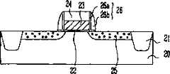
图3A至3D示出了制造根据本发明一个实施例的具有抬高的源和漏区的晶体管的方法。参见图3A,在硅衬底20上形成场氧化隔离结构21,以限定有源区和无源区。形成于有源区上的栅结构包括设置于硅衬底上栅氧化膜22、叠置栅氧化膜上的栅极23、及叠置于栅极上的掩蔽绝缘膜24。3A to 3D illustrate a method of fabricating a transistor with elevated source and drain regions according to one embodiment of the present invention. Referring to FIG. 3A , a field
然后,邻近栅结构的端部,在衬底20中形成中度掺杂区25。为此,在一个实施例中,在低能量下进行离子注入步骤。例如,为制造NMOS晶体管,以约5Kev至约10keV的低能量,向衬底的要求区中注入砷离子。离子注入一直进行到目标区达到约1014/cm3至约7×1012/cm3的杂质浓度,以形成中度掺杂的区25。区25的结深约为600埃。在不同的实施方式中,可以用不同的方法。例如,如果在用除砷离子外的离子进行离子注入时,需要用不同的能量水平、不同的杂质浓度、不同的结深或它们的组合。A moderately
参见图3B,形成了中度掺杂区25后,在衬底上依次淀积氧化膜26a和氮化膜26b,每个膜的厚度为约100到约300埃。一般说,希望氧化膜26a形成为100到200埃厚,而氮化膜26b形成为200到300埃厚。此后,选择地去掉氧化和氮化膜,形成双栅间隔层26。一般用毯式干法腐蚀选择性去除这些膜,并形成栅间隔层26。Referring to FIG. 3B, after the moderately
参见图3C,形成轻掺杂硅层27首先包括去掉衬底上的自然氧化膜(未示出)。根据一个实施例,利用非现场清洗法去掉自然氧化,该方法包括从处理室中取出衬底,并将衬底浸入例如HF等清洗液,并进行RCA或UV臭氧清洗。然后,再将衬底放入处理室。在氢气氛中烘烤衬底,即,在约800到900℃的温度下,进行1-5分钟的氢烘焙,从而防止在衬底上生长氧化物。控制非现场清洗方法和氢烘焙,用以去掉氮化膜26b下的氧化膜26a的选定部分,从而在氮化膜下形成底切。该底切从栅氧化膜22的一端起停止在约100埃处。Referring to FIG. 3C , forming the lightly doped
氢烘焙后,在中度掺杂区25上形成轻掺杂硅层或轻掺杂外延硅层27。在一个实施例中,通过利用低压汽相淀积法(“LPCVD”),在硅衬底20的暴露部分上选择性生长外延层,形成轻掺杂硅层27。LPCVD工艺的工艺方法包括使约30sccm到约300sccm的二氯硅烷(DCS:SiH2Cl2)、约30sccm到约200sccm的HCl和约100sccm到约300sccm磷化氢流入处理室用于掺杂。处理室保持在约10乇到约50乇的压力下,约750到950℃的温度下。淀积工艺进行约10分钟,从而提供厚约500到约2000埃的轻掺杂外延硅层27。After hydrogen baking, a lightly doped silicon layer or a lightly doped
如图3C所示,邻接双栅间隔层26生长的外延硅层27低于其它区。结果,邻接双栅间隔层26,在外延硅层27的表面处形成刻面28。然而,由于本实施例下,在LPCVD方法期间,轻掺杂外延硅层即自对准外延硅毛刺29(“SESS”)生长于底切内,所以,刻面28比常规方法下形成的刻面18小许多。首先,由于与常规SESS的约1/4的氧化物/氮化物厚度比相比,氧化物/氮化物厚度之比增大到高达约2/3,第二,由于轻掺杂选择性外延生长可以使所说刻面的生长速率较低,所以,该轻掺杂SESS29有助于减小刻面28的尺寸。一般说,根据本发明一个实施例的刻面28的尺寸小于100埃。As shown in FIG. 3C, the
参见图3D,进行离子注入步骤,在外延硅层27上形成重掺杂区27a。在一个实施例中,为制造NMOS晶体管,离子注入步骤包括以约5keV到约10keV的低能量,向外延硅层注入砷离子,深度约300埃。能量水平选择为使离子不会在外延硅层中推进得太远,以便该外延硅层的下部保持轻掺杂。该离子注入一直进行到目标区达到约1015/cm3到约5×1015/cm3的杂质浓度水平。达到希望的杂质浓度水平后,进行预定时间的退火工艺,激活注入到外延硅层中的离子,形成厚度约为外延硅层1/2的重掺杂区27a。1/2以下的厚度保持轻掺杂。Referring to FIG. 3D , an ion implantation step is performed to form a heavily doped region 27 a on the
在一个实施例中,可以不用离子注入步骤形成重掺杂区27a和轻掺杂区27b。例如,可以通过进行第一CVD法生长轻掺杂区27b,然后,变为第二CVD法生长重掺杂区27a,形成这些区。In one embodiment, the heavily doped region 27a and the lightly doped region 27b may be formed without an ion implantation step. For example, these regions can be formed by performing the first CVD method to grow the lightly doped region 27b, and then changing to the second CVD method to grow the heavily doped region 27a.
再参见上述实施例,控制退火工艺,使外延硅层27的上部变为重掺杂,而下部保持轻掺杂。在一个实施例中,在反应炉中进行退火工艺时,在约800到约950℃的温度下,在氮气氛中,进行约10到30分钟退火。在另一实施例中,在快速热退火炉中进行该退火工艺,在约900到约1050℃的温度下,在含N2的气氛中进行退火约1到30秒,其中温度以约每秒30到200℃的增幅升高。Referring to the above embodiment again, the annealing process is controlled so that the upper part of the
由上述工艺,可以形成具有带结257的抬高源和漏区的晶体管。结257包括依次叠置的中度掺杂区25、轻掺杂区27b和重掺杂区27a。From the process described above, a transistor with elevated source and drain regions with junction 257 can be formed. The junction 257 includes a moderately doped
图4比较了常规晶体管和根据本发明上述方法形成的晶体管(“新晶体管”)的电聚集现象。x轴示出了从栅的中心起的距离,y轴示出了电场强度。如图所示,在常规晶体管和新晶体管中,在栅和漏结附近都观察到了电场中的尖峰。然而,新晶体管一般具有幅度低于常规晶体管的尖峰。结果,新晶体管更有效地抑制了热载流子,减小了短沟道阈值电压滑离。相信这些效果是由于形成轻掺杂的自对准外延硅毛刺29,并使形成的刻面最小的缘故。FIG. 4 compares the electrical accumulation phenomenon of a conventional transistor and a transistor formed according to the above-described method of the present invention ("new transistor"). The x-axis shows the distance from the center of the grid and the y-axis shows the electric field strength. As shown, spikes in the electric field are observed near the gate and drain junctions in both conventional and new transistors. However, new transistors generally have spikes that are lower in magnitude than conventional transistors. As a result, the new transistor suppresses hot carriers more effectively, reducing short channel threshold voltage slip-off. These effects are believed to be due to the formation of lightly doped self-aligned epitaxial silicon burrs 29, with minimal facet formation.
尽管充分介绍了特定实施例,但可以使用各种改进、替代结构和等效结构等。因此,上述介绍和附图不应限制由所附权利要求书限定的本发明的范围。While specific embodiments have been sufficiently described, various modifications, alternative constructions, equivalent constructions, etc., may be used. Accordingly, the above description and drawings should not limit the scope of the invention, which is defined by the appended claims.
Claims (17)
Applications Claiming Priority (2)
| Application Number | Priority Date | Filing Date | Title |
|---|---|---|---|
| KR25429/1999 | 1999-06-29 | ||
| KR1019990025429AKR100332106B1 (en) | 1999-06-29 | 1999-06-29 | Method of manufacturing a transistor in a semiconductor device |
Publications (2)
| Publication Number | Publication Date |
|---|---|
| CN1284743Atrue CN1284743A (en) | 2001-02-21 |
| CN1146972C CN1146972C (en) | 2004-04-21 |
Family
ID=19597158
Family Applications (1)
| Application Number | Title | Priority Date | Filing Date |
|---|---|---|---|
| CNB00109713XAExpired - Fee RelatedCN1146972C (en) | 1999-06-29 | 2000-06-29 | Method of fabricating a transistor with elevated drain in a substrate |
Country Status (7)
| Country | Link |
|---|---|
| US (1) | US6368927B1 (en) |
| JP (1) | JP2001068671A (en) |
| KR (1) | KR100332106B1 (en) |
| CN (1) | CN1146972C (en) |
| DE (1) | DE10031624B4 (en) |
| GB (1) | GB2355583B (en) |
| TW (1) | TW457595B (en) |
Cited By (3)
| Publication number | Priority date | Publication date | Assignee | Title |
|---|---|---|---|---|
| CN1314092C (en)* | 2003-01-02 | 2007-05-02 | 联华电子股份有限公司 | Method of making semiconductor element |
| CN102956502A (en)* | 2011-08-18 | 2013-03-06 | 南亚科技股份有限公司 | Method of fabricating a recessed channel access transistor device |
| CN110867412A (en)* | 2019-11-19 | 2020-03-06 | 上海华力微电子有限公司 | Manufacturing method of MOS device |
Families Citing this family (30)
| Publication number | Priority date | Publication date | Assignee | Title |
|---|---|---|---|---|
| US6703688B1 (en) | 2001-03-02 | 2004-03-09 | Amberwave Systems Corporation | Relaxed silicon germanium platform for high speed CMOS electronics and high speed analog circuits |
| US6830976B2 (en) | 2001-03-02 | 2004-12-14 | Amberwave Systems Corproation | Relaxed silicon germanium platform for high speed CMOS electronics and high speed analog circuits |
| US7176109B2 (en) | 2001-03-23 | 2007-02-13 | Micron Technology, Inc. | Method for forming raised structures by controlled selective epitaxial growth of facet using spacer |
| US6566198B2 (en)* | 2001-03-29 | 2003-05-20 | International Business Machines Corporation | CMOS structure with non-epitaxial raised source/drain and self-aligned gate and method of manufacture |
| US6660635B1 (en)* | 2002-03-20 | 2003-12-09 | Taiwan Semiconductor Manufacturing Company | Pre-LDD wet clean recipe to gain channel length scaling margin beyond sub-0.1 μm |
| KR100479971B1 (en)* | 2002-05-02 | 2005-03-30 | 동부아남반도체 주식회사 | Gate through implant process |
| US6995430B2 (en) | 2002-06-07 | 2006-02-07 | Amberwave Systems Corporation | Strained-semiconductor-on-insulator device structures |
| US6946371B2 (en) | 2002-06-10 | 2005-09-20 | Amberwave Systems Corporation | Methods of fabricating semiconductor structures having epitaxially grown source and drain elements |
| US6982474B2 (en) | 2002-06-25 | 2006-01-03 | Amberwave Systems Corporation | Reacted conductive gate electrodes |
| KR100575617B1 (en)* | 2002-07-11 | 2006-05-03 | 매그나칩 반도체 유한회사 | Drain Formation Method of Semiconductor Device |
| US7473947B2 (en)* | 2002-07-12 | 2009-01-06 | Intel Corporation | Process for ultra-thin body SOI devices that incorporate EPI silicon tips and article made thereby |
| WO2004081982A2 (en) | 2003-03-07 | 2004-09-23 | Amberwave Systems Corporation | Shallow trench isolation process |
| US6911367B2 (en)* | 2003-04-18 | 2005-06-28 | Micron Technology, Inc. | Methods of forming semiconductive materials having flattened surfaces; methods of forming isolation regions; and methods of forming elevated source/drain regions |
| KR101035643B1 (en)* | 2003-11-10 | 2011-05-19 | 매그나칩 반도체 유한회사 | Manufacturing Method of Semiconductor Device |
| US7335959B2 (en)* | 2005-01-06 | 2008-02-26 | Intel Corporation | Device with stepped source/drain region profile |
| US7579617B2 (en)* | 2005-06-22 | 2009-08-25 | Fujitsu Microelectronics Limited | Semiconductor device and production method thereof |
| JP4984665B2 (en)* | 2005-06-22 | 2012-07-25 | 富士通セミコンダクター株式会社 | Semiconductor device and manufacturing method thereof |
| US7541239B2 (en)* | 2006-06-30 | 2009-06-02 | Intel Corporation | Selective spacer formation on transistors of different classes on the same device |
| KR100781549B1 (en) | 2006-11-03 | 2007-12-03 | 삼성전자주식회사 | Method for manufacturing a semiconductor integrated circuit device and semiconductor integrated circuit device manufactured thereby |
| KR100898225B1 (en) | 2007-09-07 | 2009-05-18 | 주식회사 동부하이텍 | Semiconductor device and manufacturing method thereof |
| KR100915165B1 (en)* | 2007-12-27 | 2009-09-03 | 주식회사 하이닉스반도체 | Method for fabricating semiconductor device |
| US8778767B2 (en)* | 2010-11-18 | 2014-07-15 | Taiwan Semiconductor Manufacturing Company, Ltd. | Integrated circuits and fabrication methods thereof |
| US8900958B2 (en) | 2012-12-19 | 2014-12-02 | Taiwan Semiconductor Manufacturing Company, Ltd. | Epitaxial formation mechanisms of source and drain regions |
| US8853039B2 (en) | 2013-01-17 | 2014-10-07 | Taiwan Semiconductor Manufacturing Company, Ltd. | Defect reduction for formation of epitaxial layer in source and drain regions |
| US9293534B2 (en) | 2014-03-21 | 2016-03-22 | Taiwan Semiconductor Manufacturing Company, Ltd. | Formation of dislocations in source and drain regions of FinFET devices |
| US20160056261A1 (en)* | 2014-08-22 | 2016-02-25 | Globalfoundries Inc. | Embedded sigma-shaped semiconductor alloys formed in transistors |
| CN105448916B (en)* | 2014-08-29 | 2018-10-16 | 中芯国际集成电路制造(上海)有限公司 | Transistor and forming method thereof |
| CN105826201A (en)* | 2015-01-09 | 2016-08-03 | 中芯国际集成电路制造(上海)有限公司 | Method for forming semiconductor device |
| US10079261B1 (en)* | 2017-08-17 | 2018-09-18 | Omnivision Technologies, Inc. | Raised electrode to reduce dark current |
| CN116133380B (en)* | 2021-08-25 | 2025-09-12 | 长鑫存储技术有限公司 | Semiconductor structure and method for forming the same |
Family Cites Families (60)
| Publication number | Priority date | Publication date | Assignee | Title |
|---|---|---|---|---|
| JPS54158880A (en) | 1978-06-06 | 1979-12-15 | Matsushita Electric Ind Co Ltd | Compound semiconductor device and its manufacture |
| US5032538A (en) | 1979-08-10 | 1991-07-16 | Massachusetts Institute Of Technology | Semiconductor embedded layer technology utilizing selective epitaxial growth methods |
| US4404732A (en)* | 1981-12-07 | 1983-09-20 | Ibm Corporation | Self-aligned extended epitaxy mesfet fabrication process |
| EP0197424B1 (en)* | 1985-03-25 | 1993-06-02 | Nec Corporation | Process of fabricating a heterojunction bipolar transistor |
| US4738937A (en) | 1985-10-22 | 1988-04-19 | Hughes Aircraft Company | Method of making ohmic contact structure |
| JPS62291176A (en)* | 1986-06-11 | 1987-12-17 | Hitachi Ltd | Semiconductor device and manufacture thereof |
| KR880010481A (en) | 1987-02-21 | 1988-10-10 | 강진구 | Liquid Thin Film Crystal Growth Method and Apparatus |
| US5322814A (en) | 1987-08-05 | 1994-06-21 | Hughes Aircraft Company | Multiple-quantum-well semiconductor structures with selective electrical contacts and method of fabrication |
| US5594280A (en) | 1987-10-08 | 1997-01-14 | Anelva Corporation | Method of forming a thin film and apparatus of forming a metal thin film utilizing temperature controlling means |
| JPH01105529A (en) | 1987-10-19 | 1989-04-24 | Toshiba Corp | Manufacture of semiconductor device |
| JPH0237745A (en) | 1988-07-28 | 1990-02-07 | Oki Electric Ind Co Ltd | Manufacture of semiconductor device |
| US5030583A (en) | 1988-12-02 | 1991-07-09 | Advanced Technolgy Materials, Inc. | Method of making single crystal semiconductor substrate articles and semiconductor device |
| JPH02260667A (en) | 1989-03-31 | 1990-10-23 | Mitsubishi Electric Corp | Compound semiconductor solar cell on silicon substrate and its manufacturing method |
| US5378652A (en) | 1989-04-19 | 1995-01-03 | Kabushiki Kaisha Toshiba | Method of making a through hole in multi-layer insulating films |
| KR920008886B1 (en) | 1989-05-10 | 1992-10-10 | 삼성전자 주식회사 | DRAM cell and manufacturing method thereof |
| JPH03280551A (en)* | 1990-03-29 | 1991-12-11 | Sony Corp | Manufacture of thin film transistor |
| US5168072A (en)* | 1990-10-12 | 1992-12-01 | Texas Instruments Incorporated | Method of fabricating an high-performance insulated-gate field-effect transistor |
| JP2656397B2 (en) | 1991-04-09 | 1997-09-24 | 三菱電機株式会社 | Method for manufacturing visible light laser diode |
| US5212112A (en)* | 1991-05-23 | 1993-05-18 | At&T Bell Laboratories | Selective epitaxy of silicon in silicon dioxide apertures with suppression of unwanted formation of facets |
| JP3229012B2 (en) | 1992-05-21 | 2001-11-12 | 株式会社東芝 | Method for manufacturing semiconductor device |
| US5633201A (en) | 1992-11-30 | 1997-05-27 | Hyundai Electronics Industries, Co., Ltd. | Method for forming tungsten plugs in contact holes of a semiconductor device |
| US5322802A (en) | 1993-01-25 | 1994-06-21 | North Carolina State University At Raleigh | Method of fabricating silicon carbide field effect transistor |
| EP0671770B1 (en) | 1993-02-09 | 2000-08-02 | GENERAL SEMICONDUCTOR, Inc. | Multilayer epitaxy for a silicon diode |
| KR100320364B1 (en) | 1993-03-23 | 2002-04-22 | 가와사키 마이크로 엘렉트로닉스 가부시키가이샤 | Metal wiring and its formation method |
| JPH06296060A (en) | 1993-04-08 | 1994-10-21 | Mitsubishi Electric Corp | Method for manufacturing semiconductor visible laser diode |
| JPH07131007A (en)* | 1993-11-02 | 1995-05-19 | Tadahiro Omi | Semiconductor device |
| US5494837A (en) | 1994-09-27 | 1996-02-27 | Purdue Research Foundation | Method of forming semiconductor-on-insulator electronic devices by growing monocrystalline semiconducting regions from trench sidewalls |
| JP2964925B2 (en)* | 1994-10-12 | 1999-10-18 | 日本電気株式会社 | Method of manufacturing complementary MIS type FET |
| JP2586345B2 (en) | 1994-10-14 | 1997-02-26 | 日本電気株式会社 | Semiconductor device comprising cobalt silicide film and method of manufacturing the device |
| US5683924A (en)* | 1994-10-31 | 1997-11-04 | Sgs-Thomson Microelectronics, Inc. | Method of forming raised source/drain regions in a integrated circuit |
| EP0785573B1 (en)* | 1994-10-31 | 2005-12-14 | STMicroelectronics, Inc. | Method of forming raised source/drain regions in an integrated circuit |
| EP0709880A3 (en)* | 1994-10-31 | 1996-10-23 | Sgs Thomson Microelectronics | Process for the formation of raised source and drain zones in integrated circuits |
| US5710450A (en)* | 1994-12-23 | 1998-01-20 | Intel Corporation | Transistor with ultra shallow tip and method of fabrication |
| US5677219A (en) | 1994-12-29 | 1997-10-14 | Siemens Aktiengesellschaft | Process for fabricating a DRAM trench capacitor |
| WO1996030946A1 (en)* | 1995-03-29 | 1996-10-03 | Hitachi, Ltd. | Semiconductor device and its manufacture |
| JPH08330582A (en)* | 1995-06-02 | 1996-12-13 | Oki Electric Ind Co Ltd | Mosfet and its manufacture |
| US5504031A (en)* | 1995-07-03 | 1996-04-02 | Taiwan Semiconductor Manufacturing Company Ltd. | Elevated source/drain with solid phase diffused source/drain extension for deep sub-micron mosfets |
| JPH0945907A (en) | 1995-07-28 | 1997-02-14 | Nec Corp | Manufacture of semiconductor device |
| US5637518A (en)* | 1995-10-16 | 1997-06-10 | Micron Technology, Inc. | Method of making a field effect transistor having an elevated source and an elevated drain |
| US5753555A (en)* | 1995-11-22 | 1998-05-19 | Nec Corporation | Method for forming semiconductor device |
| JP2848299B2 (en)* | 1995-12-21 | 1999-01-20 | 日本電気株式会社 | Semiconductor device and manufacturing method thereof |
| EP0813234A3 (en)* | 1996-06-12 | 1999-05-26 | Texas Instruments Incorporated | Method of manufacturing a MOSFET |
| JP2894283B2 (en)* | 1996-06-27 | 1999-05-24 | 日本電気株式会社 | Method for manufacturing semiconductor device |
| US5677214A (en)* | 1996-09-05 | 1997-10-14 | Sharp Microelectronics Technology, Inc. | Raised source/drain MOS transistor with covered epitaxial notches and fabrication method |
| JP2964960B2 (en) | 1996-09-27 | 1999-10-18 | 日本電気株式会社 | Semiconductor device and manufacturing method thereof |
| US5804470A (en) | 1996-10-23 | 1998-09-08 | Advanced Micro Devices, Inc. | Method of making a selective epitaxial growth circuit load element |
| US5773350A (en) | 1997-01-28 | 1998-06-30 | National Semiconductor Corporation | Method for forming a self-aligned bipolar junction transistor with silicide extrinsic base contacts and selective epitaxial grown intrinsic base |
| DE19718167C1 (en)* | 1997-04-29 | 1998-06-18 | Siemens Ag | MOS transistor with shallow source-drain regions |
| JPH10335660A (en)* | 1997-06-05 | 1998-12-18 | Nec Corp | Semiconductor device and manufacture thereof |
| US6723621B1 (en)* | 1997-06-30 | 2004-04-20 | International Business Machines Corporation | Abrupt delta-like doping in Si and SiGe films by UHV-CVD |
| JPH1197519A (en) | 1997-09-17 | 1999-04-09 | Sony Corp | Method for manufacturing semiconductor device |
| US6083836A (en)* | 1997-12-23 | 2000-07-04 | Texas Instruments Incorporated | Transistors with substitutionally formed gate structures and method |
| US5902125A (en)* | 1997-12-29 | 1999-05-11 | Texas Instruments--Acer Incorporated | Method to form stacked-Si gate pMOSFETs with elevated and extended S/D junction |
| US6156613A (en)* | 1998-03-02 | 2000-12-05 | Texas Instruments - Acer Incorporated | Method to form MOSFET with an elevated source/drain |
| US5970352A (en)* | 1998-04-23 | 1999-10-19 | Kabushiki Kaisha Toshiba | Field effect transistor having elevated source and drain regions and methods for manufacturing the same |
| US6200867B1 (en)* | 1998-11-17 | 2001-03-13 | Winbond Electronics Corporation | Method for forming raised source and drain |
| US6218711B1 (en)* | 1999-02-19 | 2001-04-17 | Advanced Micro Devices, Inc. | Raised source/drain process by selective sige epitaxy |
| US6190977B1 (en)* | 1999-04-30 | 2001-02-20 | Texas Instruments - Acer Incorporated | Method for forming MOSFET with an elevated source/drain |
| US6167642B1 (en)* | 1999-06-23 | 2001-01-02 | Mark A. Nardini | Tractor bucket extension device and method |
| US6171910B1 (en)* | 1999-07-21 | 2001-01-09 | Motorola Inc. | Method for forming a semiconductor device |
- 1999
- 1999-06-29KRKR1019990025429Apatent/KR100332106B1/ennot_activeExpired - Fee Related
- 2000
- 2000-06-28GBGB0015780Apatent/GB2355583B/ennot_activeExpired - Fee Related
- 2000-06-29TWTW089112805Apatent/TW457595B/ennot_activeIP Right Cessation
- 2000-06-29CNCNB00109713XApatent/CN1146972C/ennot_activeExpired - Fee Related
- 2000-06-29DEDE10031624Apatent/DE10031624B4/ennot_activeExpired - Fee Related
- 2000-06-29JPJP2000195660Apatent/JP2001068671A/enactivePending
- 2000-06-29USUS09/608,064patent/US6368927B1/ennot_activeExpired - Lifetime
Cited By (4)
| Publication number | Priority date | Publication date | Assignee | Title |
|---|---|---|---|---|
| CN1314092C (en)* | 2003-01-02 | 2007-05-02 | 联华电子股份有限公司 | Method of making semiconductor element |
| CN102956502A (en)* | 2011-08-18 | 2013-03-06 | 南亚科技股份有限公司 | Method of fabricating a recessed channel access transistor device |
| CN102956502B (en)* | 2011-08-18 | 2015-04-29 | 南亚科技股份有限公司 | Method for manufacturing a recessed channel access transistor device |
| CN110867412A (en)* | 2019-11-19 | 2020-03-06 | 上海华力微电子有限公司 | Manufacturing method of MOS device |
Also Published As
| Publication number | Publication date |
|---|---|
| GB0015780D0 (en) | 2000-08-16 |
| DE10031624A1 (en) | 2001-03-08 |
| GB2355583A (en) | 2001-04-25 |
| GB2355583B (en) | 2004-04-14 |
| KR100332106B1 (en) | 2002-04-10 |
| CN1146972C (en) | 2004-04-21 |
| DE10031624B4 (en) | 2009-01-29 |
| TW457595B (en) | 2001-10-01 |
| JP2001068671A (en) | 2001-03-16 |
| KR20010004715A (en) | 2001-01-15 |
| US6368927B1 (en) | 2002-04-09 |
Similar Documents
| Publication | Publication Date | Title |
|---|---|---|
| CN1146972C (en) | Method of fabricating a transistor with elevated drain in a substrate | |
| JP4590151B2 (en) | Manufacturing method of semiconductor device | |
| KR100301246B1 (en) | Method of manufacturing a semiconductor device | |
| KR100347544B1 (en) | Method of manufacturing a junction in a semiconductor device | |
| US6197647B1 (en) | Method of forming ultra-thin oxides with low temperature oxidation | |
| KR100332119B1 (en) | Method of manufacturing a semiconductor device | |
| KR100280809B1 (en) | Method for forming junction of semiconductor device | |
| US20030011029A1 (en) | Method for manufacturing a mosfet having deep SD regions and SD extension regions | |
| JP2733082B2 (en) | MOS device manufacturing method | |
| KR20050000059A (en) | Method of manufacturing semicondutor device | |
| JP2594772B2 (en) | MOS device and method of manufacturing the same | |
| KR100440078B1 (en) | Manufacturing method of semiconductor device | |
| KR20010061029A (en) | A method for forming MOSFET of elevated source/drain structure | |
| KR930011542B1 (en) | Manufacturing method of bipolar transistor | |
| KR100740780B1 (en) | Method of manufacturing transistor of semiconductor device | |
| US6309939B1 (en) | Method of manufacturing a semiconductor device | |
| KR100463956B1 (en) | Transistor Formation Method of Semiconductor Device | |
| KR0155512B1 (en) | Method of forming collector sinker of bipolar transistor | |
| KR100671663B1 (en) | Method of manufacturing transistor of semiconductor device | |
| KR920005127B1 (en) | Method of manufacturing self-aligned bipolar transistor using selective epitaxy | |
| KR100451768B1 (en) | Method for fabricating gate dielectric of semiconductor device | |
| KR100497221B1 (en) | Method For Manufacturing Semiconductor Devices | |
| KR100221617B1 (en) | Method of manufacturing semiconductor device | |
| KR100399948B1 (en) | Method of forming device isolation film in semiconductor device | |
| KR20050104229A (en) | Method of manufacturing semiconductor device |
Legal Events
| Date | Code | Title | Description |
|---|---|---|---|
| C06 | Publication | ||
| PB01 | Publication | ||
| C10 | Entry into substantive examination | ||
| SE01 | Entry into force of request for substantive examination | ||
| C14 | Grant of patent or utility model | ||
| GR01 | Patent grant | ||
| CF01 | Termination of patent right due to non-payment of annual fee | Granted publication date:20040421 Termination date:20150629 | |
| EXPY | Termination of patent right or utility model |