CN1282974A - Electron emitting cathode and its manufacturing method and application - Google Patents
Electron emitting cathode and its manufacturing method and applicationDownload PDFInfo
- Publication number
- CN1282974A CN1282974ACN00105457ACN00105457ACN1282974ACN 1282974 ACN1282974 ACN 1282974ACN 00105457 ACN00105457 ACN 00105457ACN 00105457 ACN00105457 ACN 00105457ACN 1282974 ACN1282974 ACN 1282974A
- Authority
- CN
- China
- Prior art keywords
- semiconductor film
- cathode
- electron emission
- film
- type semiconductor
- Prior art date
- Legal status (The legal status is an assumption and is not a legal conclusion. Google has not performed a legal analysis and makes no representation as to the accuracy of the status listed.)
- Granted
Links
Images


Classifications
- H—ELECTRICITY
- H01—ELECTRIC ELEMENTS
- H01J—ELECTRIC DISCHARGE TUBES OR DISCHARGE LAMPS
- H01J9/00—Apparatus or processes specially adapted for the manufacture, installation, removal, maintenance of electric discharge tubes, discharge lamps, or parts thereof; Recovery of material from discharge tubes or lamps
- H01J9/02—Manufacture of electrodes or electrode systems
- H01J9/022—Manufacture of electrodes or electrode systems of cold cathodes
- H01J9/025—Manufacture of electrodes or electrode systems of cold cathodes of field emission cathodes
- B—PERFORMING OPERATIONS; TRANSPORTING
- B82—NANOTECHNOLOGY
- B82Y—SPECIFIC USES OR APPLICATIONS OF NANOSTRUCTURES; MEASUREMENT OR ANALYSIS OF NANOSTRUCTURES; MANUFACTURE OR TREATMENT OF NANOSTRUCTURES
- B82Y10/00—Nanotechnology for information processing, storage or transmission, e.g. quantum computing or single electron logic
- H—ELECTRICITY
- H01—ELECTRIC ELEMENTS
- H01J—ELECTRIC DISCHARGE TUBES OR DISCHARGE LAMPS
- H01J1/00—Details of electrodes, of magnetic control means, of screens, or of the mounting or spacing thereof, common to two or more basic types of discharge tubes or lamps
- H01J1/02—Main electrodes
- H01J1/30—Cold cathodes, e.g. field-emissive cathode
- H01J1/304—Field-emissive cathodes
- H01J1/3042—Field-emissive cathodes microengineered, e.g. Spindt-type
- H—ELECTRICITY
- H01—ELECTRIC ELEMENTS
- H01J—ELECTRIC DISCHARGE TUBES OR DISCHARGE LAMPS
- H01J2201/00—Electrodes common to discharge tubes
- H01J2201/30—Cold cathodes
- H01J2201/304—Field emission cathodes
- H01J2201/30403—Field emission cathodes characterised by the emitter shape
- H—ELECTRICITY
- H01—ELECTRIC ELEMENTS
- H01J—ELECTRIC DISCHARGE TUBES OR DISCHARGE LAMPS
- H01J2201/00—Electrodes common to discharge tubes
- H01J2201/30—Cold cathodes
- H01J2201/304—Field emission cathodes
- H01J2201/30446—Field emission cathodes characterised by the emitter material
- H01J2201/30453—Carbon types
- H01J2201/30457—Diamond
- H—ELECTRICITY
- H01—ELECTRIC ELEMENTS
- H01J—ELECTRIC DISCHARGE TUBES OR DISCHARGE LAMPS
- H01J2329/00—Electron emission display panels, e.g. field emission display panels
Landscapes
- Engineering & Computer Science (AREA)
- Chemical & Material Sciences (AREA)
- Nanotechnology (AREA)
- Manufacturing & Machinery (AREA)
- Physics & Mathematics (AREA)
- Mathematical Physics (AREA)
- Theoretical Computer Science (AREA)
- Crystallography & Structural Chemistry (AREA)
- Cold Cathode And The Manufacture (AREA)
- Cathode-Ray Tubes And Fluorescent Screens For Display (AREA)
Abstract
Description
Translated fromChinese本申请是1995年10月5日递交的,题目为“电子发射阴极及其制造方法及其应用”的专利申请号为95118252.8的中国专利申请的分案申请。This application is a divisional application of the Chinese patent application No. 95118252.8 submitted on October 5, 1995, entitled "Electron Emitting Cathode and Its Manufacturing Method and Its Application".
本发明涉及一种电子发射阴极;电子发射装置,平板显示器,及包括该电子发射阴极的热电型冷却装置;及制造该电子发射阴极的方法。The present invention relates to an electron emission cathode; an electron emission device, a flat panel display, and a thermoelectric cooling device including the electron emission cathode; and a method for manufacturing the electron emission cathode.
近年来,使用半导体小型化技术来集成小型电子发射装备并旨在实现高性能装置,如超高速装置的研究已经蓬勃地开展。这个研究领域被称为“真空微电子学”。真空微电子学尤其将其注意力一直聚集在平板显示器(或场发射显示器;以下为“FEDS”)的应用上,因为用于FED的电子发射装置的使用被考虑会导致产生比传统阴极射线管显示器更薄且更轻的显示装置。In recent years, research into integrating small-sized electron emission devices using semiconductor miniaturization technology and aiming to realize high-performance devices, such as ultra-high-speed devices, has been vigorously conducted. This field of research is known as "vacuum microelectronics". Vacuum microelectronics in particular has been focusing its attention on the application of flat panel displays (or field emission displays; hereinafter "FEDS"), because the use of electron emission devices for FEDs is considered to result A display device with a thinner and lighter display.
在包括电子发射装置的FED中,电子发射装置布置成两维的排列并使得它们与其上涂有荧光物质的一个阳极相对置。利用在每个阴极与该阳极之间施加电压,使电子吸现进入真空,在那里电子将和荧光物质碰撞,致使其受激励并发射出光。In the FED including electron emission devices, the electron emission devices are arranged in a two-dimensional array such that they are opposed to an anode on which a fluorescent substance is coated. By applying a voltage between each cathode and the anode, electrons are sucked into the vacuum where they will collide with the phosphor, causing it to become excited and emit light.
以下将描述传统的电子发射装置。通常,当从一固体电极中拉出电子时,其电流在密度J根据福勒尔-诺德海姆(Fowler-Nordheim)公式(式1)来求得:J=(A·F2/φ)·exp(-B·φ3/2/F)A conventional electron emission device will be described below. Usually, when electrons are pulled out from a solid electrode, the current density J is obtained according to the Fowler-Nordheim formula (Formula 1): J=(A·F2 /φ )·exp(-B·φ3/2 /F)
在上式中,A和B代表正常数;F代表电场;及φ代表阴极的逸出功。假定当拉出电子时所施加的电压为V,电场F则根据式2来求得:In the above formula, A and B represent normal constants; F represents the electric field; and φ represents the work function of the cathode. Assuming that the applied voltage is V when the electrons are pulled out, the electric field F is obtained according to formula 2:
F=βV 式2F=βV Formula 2
在上式中,β是由阴极的几何形状决定的常数。In the above formula, β is a constant determined by the geometry of the cathode.
根据式1及式2,当保持施加电压V恒定时,通过增大β和/或减小φ可以使电流密度J增大。但是,在使用半导体作阴极的情况下,可用减小电子亲和力x(它是真空能级和半导体电带之间的能量差)取代逸出功φ来增加电流密度J。为了增大β,必须对阴极处理使其具有尖锐的点。尤其是,例如常使用蚀刻n型硅衬底并使其形成具有尖锐点突起的电子发射部分的方法。According to Equation 1 and Equation 2, when the applied voltage V is kept constant, the current density J can be increased by increasing β and/or decreasing φ. However, in the case of using a semiconductor as the cathode, the current density J can be increased by reducing the electron affinity x (which is the energy difference between the vacuum level and the electric band of the semiconductor) instead of the work function φ. In order to increase β, the cathode must be treated to have a sharp point. In particular, for example, a method of etching an n-type silicon substrate and forming an electron-emitting portion having sharp point protrusions is often used.
图18是表示具有作为电子发射部分的尖锐点突起的传统电子发射装置的概要横截面图。如图18所示,电子发射装置500包括具有电子发射部分502的硅衬底504及形成在该硅衬底504上的栅极508,在它们之间夹有一绝缘膜506并使其围绕着电子发射部分502。具有尖顶锥状的电子发射部分502是由蚀刻硅衬底504获得的。在硅衬底504上设置了一个电极510。Fig. 18 is a schematic cross-sectional view showing a conventional electron-emitting device having sharp point protrusions as electron-emitting portions. As shown in FIG. 18, an
利用将电子发射装置500放置在真空中并使其与一阳极对置,及相对于硅衬底504的电位对栅极508施加几十伏至几百伏的正电压,由于其尖顶,电场将集中在电子发射部分502上。然后,由真空度形成的势垒对于电子发射部分502中的电子来说被降低了,并且该势垒变薄了,因此由于隧道效应使电子从电子发射部分502的表面被吸出进入到真空中。被吸出的电子受到放置在硅衬底504对面的阳极的捕获,在阳极上相对栅极508的电位施加了几百至几千伏的正电压。By placing the
在仅有硅衬底504及电子发射部分502组成的电子发射阴极,没有任何栅极包括在内的情况下,电子将直接地被拉出并被对置的阳极捕获,这时在阳极及硅衬底504之间施加了几百至几千伏的电压。In the case of an electron emission cathode composed of only the
作为用来使电能转换成热能的传统热电式装置,已公知了如图19所示的热电式冷却装置520。该热电式冷却装置520具有其中通过金属板526及528使n型半导体层522和p型半导体层524彼此交替串联连接的结构。利用在端子530及532之间施加电压,可使金属板526或金属板528被冷却,而另一金属板528或526则被加热。As a conventional thermoelectric device for converting electrical energy into thermal energy, a
但是,上述传统的电子发射装置具有以下的问题。However, the conventional electron emission devices described above have the following problems.
首先,对电子发射部分的尖项必须以毫微米级的精度进行加工,因此需要高复杂的半导体处理技术。因而,用低成本来制包括这种电子发射装置的FEDS是有困难的。再者,电子发射装置的该尖顶形状易趋于改变,由此会产生由FED的非均匀显示。此外,电子发射装置的该尖顶易于被真空中的离子粒子撞击而产生溅蚀,由此会在较短的时间周期中形成该尖顶的损伤。其结果是,不能期望实现具有长寿命的FED。First, the tip of the electron emission part must be processed with nanometer-level precision, thus requiring highly complex semiconductor processing technology. Therefore, it is difficult to manufacture FEDS including such electron-emitting devices at low cost. Furthermore, the shape of the tip of the electron emission device tends to change, thereby causing non-uniform display by the FED. In addition, the tip of the electron emission device is prone to be sputtered by ion particles in the vacuum, thereby causing damage to the tip in a short period of time. As a result, it cannot be expected to realize a FED with a long lifetime.
在使用上述电子发射装置构成FED的情况下,必须实现约10-8乇(torr)的真空度。使用这种真空度的FEDS的商用生产是不现实的。In the case of constituting an FED using the above electron emission device, it is necessary to realize a vacuum degree of about 10-8 Torr. The commercial production of FEDS using this vacuum is not realistic.
此外,用作衬底的硅衬底限制了FED的显示器尺寸。这将导致实现大型显示的FED的困难问题。Furthermore, the silicon substrate used as the substrate limits the display size of the FED. This will cause a difficult problem in realizing a FED for a large display.
在传统的热电式冷却装置中,被冷却的金属板及被加热的金属板彼此通过n型半导体层522及p型半导体层524相连接。热量将通过这些半导体层522及524从被冷却的板传递到被加热的板上,这就形成了大的热泄漏。这便产生了非常低的冷却/加热效率。In a conventional thermoelectric cooling device, the metal plate to be cooled and the metal plate to be heated are connected to each other through the n-
本发明的目的在于提供一种电子发射阴极及一种电子发射装置,它们可相对地免于时效的损坏,允许构成大面积的装置,并甚至在低真空度时也能高效地发射电子并且成本低及是有优异的批量生产率。并且,提供包括该电子发射电极的一种高亮度、长寿命及大型显示的平板显示器。It is an object of the present invention to provide an electron emission cathode and an electron emission device which are relatively free from aging damage, allow the construction of large-area devices, and emit electrons efficiently and at a low cost even in a low vacuum. Low and has excellent batch productivity. And, a high-brightness, long-life, and large-scale display flat panel display including the electron emission electrode is provided.
本发明的另一目的在于提供一种包括该电子发射电极的一种重量轻、效率高及功率大的热电式冷却装置。Another object of the present invention is to provide a light-weight, high-efficiency and high-power thermoelectric cooling device including the electron emission electrode.
根据本发明的一方面,电子发射阴极包括:一个n型半导体膜,其包含从该n型半导体膜表面上部分地突出的金刚石(diamond)颗粒;及一个阳极,它被放置在n型半导体膜的对面,并在这两者间设有真空,其中利用在阳极与n型半导体膜之间施加一电压使电子发射。According to an aspect of the present invention, the electron emission cathode includes: an n-type semiconductor film, which contains diamond (diamond) particles partially protruding from the surface of the n-type semiconductor film; and an anode, which is placed on the n-type semiconductor film and a vacuum is provided between the two, in which electrons are emitted by applying a voltage between the anode and the n-type semiconductor film.
在本发明的一个实施例中,该金刚石颗粒是由p型半导体构成的。In one embodiment of the invention, the diamond particles are composed of a p-type semiconductor.
根据本发明的另一方面,电子发射阴极包括:一个碳膜,其包含从该碳膜表面上部分突出的金刚石颗粒;其中利用在一阳极与碳膜之间施加一电压使电子发射。According to another aspect of the present invention, an electron emission cathode includes: a carbon film including diamond particles partially protruding from a surface of the carbon film; wherein electrons are emitted by applying a voltage between an anode and the carbon film.
在本发明的一个实施例中,该碳膜是n型半导体或赝n型半导体。In one embodiment of the invention, the carbon film is an n-type semiconductor or a pseudo-n-type semiconductor.
在本发明的一个实施例中,该碳膜包含作为n型杂质的氮,及部分的碳膜包含具有金刚石结构的颗粒。In one embodiment of the present invention, the carbon film contains nitrogen as an n-type impurity, and part of the carbon film contains particles having a diamond structure.
根据本发明的又一方面,电子发射阴极包括:一个导电膜;形成在该导电膜上的第一导电型的一个第一半导体膜;形成在第一半导体膜上的第二导电型的一个岛状第二半体导膜;其中利用在一阳极及第二半导体膜之间施加一电压使电子发射。According to still another aspect of the present invention, the electron emission cathode includes: a conductive film; a first semiconductor film of the first conductivity type formed on the conductive film; an island of the second conductivity type formed on the first semiconductor film A second semiconductive film; wherein electrons are emitted by applying a voltage between an anode and the second semiconductive film.
在本发明的一个实施例中,第一半导体膜被作成岛状形状。In one embodiment of the present invention, the first semiconductor film is formed in an island shape.
根据本发明的另一方面,电子发射阴极包括:一个导电膜;形成在该导电膜上的第一导电型的一个第一半导体膜;形成在第一半导体膜上的并具有多个设在其中的孔的第二导电型的一个第二半导体膜,该多个孔至少曝露出第一半导体膜的一个表面;其中利用在一阳极及第二半导体膜之间施加一电压使电子发射。According to another aspect of the present invention, the electron emission cathode includes: a conductive film; a first semiconductor film of the first conductivity type formed on the conductive film; formed on the first semiconductor film and having a plurality of A second semiconductor film of the second conductivity type with holes, the plurality of holes exposing at least one surface of the first semiconductor film; wherein electrons are emitted by applying a voltage between an anode and the second semiconductor film.
在本发明的一个实施例中,在第一半导体膜上也设有多个孔,由此曝露出导电膜的一个表面。In one embodiment of the present invention, a plurality of holes are also provided in the first semiconductor film, thereby exposing one surface of the conductive film.
在本发明的一个实施例中,第一半导体膜及第二半导体膜中的一个包含掺硼的金刚石。In one embodiment of the present invention, one of the first semiconductor film and the second semiconductor film includes boron-doped diamond.
在本发明的一个实施例中,第一半导体膜及第二半导体膜中的一个是由含氮的薄碳膜构成的,该薄碳膜是利用由吡啶(pyridine)、哒嗪(pyridazine)、嘧啶(pyrimidine)、及1,3,5-三嗪(triazine)组成的族中选择出的一个的制成的。In one embodiment of the present invention, one of the first semiconductor film and the second semiconductor film is made of a nitrogen-containing thin carbon film made of pyridine, pyridazine, A product selected from the group consisting of pyrimidine and 1,3,5-triazine.
根据本发明的又一方面,电子发射装置包括:一个由-n型半导体膜组成的阴极,该膜包含部分地从该n型半导体膜的表面突出的金刚石颗粒;及一个与该n型半导体膜对置的阳极并在这两者之间设有真空,其中利用在阳极及阴极之间施加一电压使电子从阴极发射出来。According to yet another aspect of the present invention, an electron emission device includes: a cathode composed of an n-type semiconductor film including diamond particles partially protruding from the surface of the n-type semiconductor film; Opposite anodes with a vacuum between them, wherein electrons are emitted from the cathode by applying a voltage between the anode and cathode.
根据本发明的另一方面,电子发射装置包括;一个由碳膜组成的阴极,该碳膜包含部分地从该碳膜表面突出的金刚石颗粒;及一个与该碳膜对置的阳极并在这两者之间设有真空,其中利用在阳极及阴极之间施加一电压使电子从阴极发射出来。According to another aspect of the present invention, an electron emission device includes; a cathode composed of a carbon film containing diamond particles partially protruding from the surface of the carbon film; A vacuum is provided between the two, where electrons are emitted from the cathode by applying a voltage between the anode and the cathode.
根据本发明的又一方面,电子发射装置包括;一个阴极,它包括一个导电膜,形成在该导电膜上的第一导电型的一个第一半导体膜,及形成在第一半导体膜上的第二导电型的一个岛状第二半导体膜;及与第一半导体膜对置的一个阳极并在这两者之间设有真空,其中利用在阳极及阴极之间施加一电压使电子从阴极发射出来。According to yet another aspect of the present invention, an electron emission device includes; a cathode including a conductive film, a first semiconductor film of a first conductivity type formed on the conductive film, and a first semiconductor film formed on the first semiconductor film. An island-shaped second semiconductor film of two conductivity types; and an anode opposite to the first semiconductor film with a vacuum provided therebetween, wherein electrons are emitted from the cathode by applying a voltage between the anode and the cathode come out.
根据本发明的另一方面,电子发射装置包括:一个阴极,它包括一个导电膜,形成在该导电膜上的第一导电型的一个第一半导体膜,及形成在第一半导体膜上的并具有多个设在其中的孔的第二导电型的一个第二半导体膜,该多个孔至少曝露出第一半导体膜的一个表面;及与第一半导体膜对置的一个阳极并在这两者之间设有真空,其中利用在阳极及阴极之间施加一电压使电子从阴极发射出来。According to another aspect of the present invention, an electron emission device includes: a cathode including a conductive film, a first semiconductor film of a first conductivity type formed on the conductive film, and a first semiconductor film formed on the first semiconductor film. a second semiconductor film of the second conductivity type having a plurality of holes provided therein exposing at least one surface of the first semiconductor film; and an anode opposite to the first semiconductor film and between the two There is a vacuum between them, and electrons are emitted from the cathode by applying a voltage between the anode and the cathode.
在本发明的一个实施例中,该电子发射装置还包括设在阴极与阳极之间的一个栅极,该栅极具有孔,用于至少曝露阴极的一部分,其中利用在栅极上施加一电压使电子从阴极拉出。In one embodiment of the present invention, the electron emission device further includes a grid disposed between the cathode and the anode, the grid has holes for exposing at least a part of the cathode, wherein by applying a voltage to the grid Electrons are pulled from the cathode.
在本发明的一个实施例中,阴极及栅极被作成沿不同方向延伸的条,以致彼此相交叉,及该孔被设置成阴极与栅极交叉处中的孔。In one embodiment of the invention, the cathode and the grid are formed as strips extending in different directions so as to intersect each other, and the hole is provided as a hole in the intersection of the cathode and the grid.
根据本发明的又一方面,平板显示器包括:一个支承衬底;一个设在支承衬底上的阴极,它由一个n型半导体膜组成,该膜包含部分地从该n型半导体膜的表面突出的金刚石颗粒;一个透明衬底;及设置在透明电极表面的荧光物质,其中支承衬底及透明衬底以这种方式布置,即阴极与荧光物质成彼此对置,及在支承衬底及透明衬底之间的内空间中设有一真空。According to still another aspect of the present invention, a flat panel display includes: a supporting substrate; a cathode provided on the supporting substrate, which is composed of an n-type semiconductor film including a part protruding from the surface of the n-type semiconductor film. diamond particles; a transparent substrate; and a fluorescent substance arranged on the surface of the transparent electrode, wherein the support substrate and the transparent substrate are arranged in such a way that the cathode and the fluorescent substance are opposite to each other, and the support substrate and the transparent A vacuum is provided in the inner space between the substrates.
根据本发明的另一方面,平板显示器包括:一个支承衬底;一个设在支承衬底上的阴极,它由碳膜组成,该碳膜包含部分地从该碳膜表面突出的金刚石颗粒;一个透明衬底;及设置在透明电极表面的荧光物质,其中支承衬底及透明衬底以这种方式布置,即阴极与荧光物质成彼此对置,及在支承衬底及透明衬底之间的内空间中设有一个真空。According to another aspect of the present invention, a flat panel display includes: a support substrate; a cathode provided on the support substrate, which consists of a carbon film comprising diamond particles partially protruding from the surface of the carbon film; a a transparent substrate; and a fluorescent substance arranged on the surface of the transparent electrode, wherein the support substrate and the transparent substrate are arranged in such a manner that the cathode and the fluorescent substance are opposed to each other, and the gap between the support substrate and the transparent substrate A vacuum is provided in the inner space.
根据本发明的又一方面,平板显示器包括;一个支承衬底;一个设在支承衬底上的阴极,该阴极包括一个导电膜,形成在该导电膜上的第一导电型的一个第一半导体膜,及形成在第一半导体膜上的第二导电型的一个岛状第二半导体膜;一个透明衬底;及设置在透明电极表面的荧光物质,其中支承衬底及透明衬底以这种方式布置,即阴极与荧光物质成彼此对置,及在支承衬底及透明衬底之间的内空间中设有一真空。According to yet another aspect of the present invention, a flat panel display includes; a support substrate; a cathode provided on the support substrate, the cathode comprising a conductive film, a first semiconductor of the first conductivity type formed on the conductive film film, and an island-shaped second semiconductor film of the second conductivity type formed on the first semiconductor film; a transparent substrate; Arranged in a manner, that is, the cathode and the phosphor are opposed to each other, and a vacuum is provided in the inner space between the supporting substrate and the transparent substrate.
根据本发明的另一方面,平板显示器包括:一个支承衬底;一个阴极,它包括一个导电膜,形成在该导电膜上的第一导电型的一个第一半导体膜,及形成在第一半导体膜上的并具有多个设在其中的孔的第二导电型的一个第二半导体膜,该多个孔至少曝露出第一半导体膜的一个表面;一个透明衬底;及设置在透明电极表面的荧光物质,其中支承衬底及透明衬底以这种方式布置,即阴极与荧光物质成彼此对置,及在支承衬底及透明衬底之间的内空间中设有一真空。According to another aspect of the present invention, a flat panel display includes: a supporting substrate; a cathode including a conductive film, a first semiconductor film of the first conductivity type formed on the conductive film, and a first semiconductor film formed on the first semiconductor film. A second semiconductor film of the second conductivity type on the film and having a plurality of holes disposed therein exposing at least one surface of the first semiconductor film; a transparent substrate; and disposed on the surface of the transparent electrode The phosphor, wherein the support substrate and the transparent substrate are arranged in such a manner that the cathode and the phosphor are opposed to each other, and a vacuum is provided in the inner space between the support substrate and the transparent substrate.
在本发明的一个实施例中,该平板显示器还包括设在阴极与荧光物质之间的一个栅极,该栅极具有孔,用于至少曝露阴极的一部分,其中利用在栅极上施加一电压使电子从阴极拉出。In one embodiment of the present invention, the flat panel display further includes a grid arranged between the cathode and the phosphor, the grid has holes for exposing at least a part of the cathode, wherein a voltage is applied to the grid Electrons are pulled from the cathode.
在本发明的一个实施例中,阴极及栅极被作成沿不同方向延伸的条,以致彼此交叉,及该孔也被设置在阴极与栅极交叉处中。In one embodiment of the invention, the cathode and the grid are formed as strips extending in different directions so as to intersect each other, and the hole is also provided in the intersection of the cathode and the grid.
根据本发明的又一方面,热电式冷却装置包括:具有一个表面的第一导电衬底;形成在第一导电衬底表面上的一个阴极;及与第一导电衬底表面对置的第二导电衬底及在它们之间设有一真空,其中电压施加在第一导电衬底与第二导电衬底之间,由此使电子从阴极经真空进入第二导电衬底,及在第一导电衬底及第二导电衬底之间流过电流,因此获得吸热效应并使第一导电衬底冷却。According to still another aspect of the present invention, the thermoelectric cooling device includes: a first conductive substrate having a surface; a cathode formed on the surface of the first conductive substrate; and a second electrode opposite to the first conductive substrate surface. Conductive substrates and a vacuum is provided between them, wherein a voltage is applied between the first conductive substrate and the second conductive substrate, so that electrons enter the second conductive substrate from the cathode through the vacuum, and in the first conductive substrate A current flows between the substrate and the second conductive substrate, thereby obtaining a heat absorption effect and cooling the first conductive substrate.
在本发明的一个实施例中,阴极是由一个n型半导体膜组成的,该膜包含部分地从该n型半导体膜表面上突出的金刚石颗粒。In one embodiment of the present invention, the cathode is composed of an n-type semiconductor film containing diamond particles partially protruding from the surface of the n-type semiconductor film.
在本发明的一个实施例中,阴极由一个碳膜组成,该碳膜包含部分地从该碳膜表面突出的金刚石颗粒。In one embodiment of the invention, the cathode consists of a carbon film comprising diamond particles partially protruding from the surface of the carbon film.
在本发明的一个实施例中,阴极包括一个导电膜,形成在该导电膜上的第一导电型的一个第一半导体膜,及形成在第一半导体膜上的并具有多个设在其中的孔的第二导电型的一个第二半导体膜,该多个孔至少曝露出第一半导体膜的一个表面。In one embodiment of the present invention, the cathode includes a conductive film, a first semiconductor film of the first conductivity type formed on the conductive film, and a first semiconductor film formed on the first semiconductor film and having a plurality of A second semiconductor film of a second conductivity type with holes, the plurality of holes exposing at least one surface of the first semiconductor film.
在本发明的一个实施例中,阴极包括具有一个低逸出功的表面的材料。In one embodiment of the invention, the cathode comprises a material having a low work function surface.
在本发明的一个实施例中,阴极包括多个微小突起。In one embodiment of the present invention, the cathode includes a plurality of tiny protrusions.
在本发明的一个实施例中,阴极是由一种半导体组成的。In one embodiment of the invention, the cathode is composed of a semiconductor.
在本发明的一个实施例中,第一导电衬底及第二导电衬底分别是两个同轴的圆筒的侧面。In one embodiment of the present invention, the first conductive substrate and the second conductive substrate are respectively the side surfaces of two coaxial cylinders.
在本发明的一个实施例中,第一导电衬底及第二导电衬底各具有肋条。In one embodiment of the present invention, each of the first conductive substrate and the second conductive substrate has ribs.
在本发明的一个实施例中,第一导电衬底及第二导电衬底以约100um或更小的间隔布置。In one embodiment of the present invention, the first conductive substrate and the second conductive substrate are arranged at an interval of about 100 um or less.
根据本发明的另一方面,用于制造电子发射阴极的方法包括下列步骤:制备包括金刚石颗粒及n型半导体粉末或碳粉末的糊剂;将该糊剂涂在一个衬底上;及烧结涂在衬底上的糊剂。According to another aspect of the present invention, a method for manufacturing an electron emission cathode includes the steps of: preparing a paste including diamond particles and n-type semiconductor powder or carbon powder; applying the paste on a substrate; and sintering Paste applied to the substrate.
根据本发明的另一方面,用于制造电子发射阴极的方法包括下列步骤:在一衬底上散布金刚石颗粒;及形成其厚度小于金刚石颗粒的颗粒直径及部分具有金刚石结构的碳膜。According to another aspect of the present invention, a method for manufacturing an electron emission cathode includes the steps of: dispersing diamond particles on a substrate; and forming a carbon film having a thickness smaller than the particle diameter of the diamond particles and partially having a diamond structure.
根据本发明的另一方面,用于制造电子发射阴极的方法包括下列步骤:形成部分具有金刚石结构的碳膜;及将金刚石颗粒加入到碳膜中。According to another aspect of the present invention, a method for manufacturing an electron emission cathode includes the steps of: forming a carbon film partially having a diamond structure; and incorporating diamond particles into the carbon film.
因此,这里所描述的本发明实现了下列优点:(1)提供了低成本及高寿命的电子发射阴极,它具有高的生产率并能够提供大的显示面积;(2)提供了包括该电子发射阴极的电子发射装置;(3)提供了包括该电子发射阴极或电子发射装置的平板显示器;及(4)提供了包括该电子发射阴极或电子发射装置的高效热电式装置。Accordingly, the invention described here achieves the following advantages: (1) provides a low-cost and long-life electron emission cathode that has high productivity and can provide a large display area; (2) provides (3) providing a flat panel display including the electron emitting cathode or electron emitting device; and (4) providing a high-efficiency thermoelectric device including the electron emitting cathode or electron emitting device.
当阅读及理解了以下参照附图的详细说明时,对熟悉本领域的技术人员来说,本发明的这些及另外的优点将会变得清楚。These and other advantages of the present invention will become apparent to those skilled in the art upon reading and understanding the following detailed description with reference to the accompanying drawings.
图1A是根据本发明例1的一个电子发射装置的透视图;1A is a perspective view of an electron emission device according to Example 1 of the present invention;
图1B是根据本发明例1的另一个电子发射装置的透视图;1B is a perspective view of another electron emission device according to Example 1 of the present invention;
图2是用于图1中电子发射装置的一个电子发射阴极的透视图;FIG. 2 is a perspective view of an electron emission cathode used in the electron emission device of FIG. 1;
图3是根据本发明的另一电子发射阴极的透视图;Figure 3 is a perspective view of another electron emission cathode according to the present invention;
图4A是根据本发明例2的一个电子发射装置的透视图;4A is a perspective view of an electron emission device according to Example 2 of the present invention;
图4B是图4A中的电子发射装置的横截面图;4B is a cross-sectional view of the electron emission device in FIG. 4A;
图4C是根据本发明例2的另一电子发射装置的横截面图;4C is a cross-sectional view of another electron emission device according to Example 2 of the present invention;
图5是根据本发明的另一电子发射装置的横截面图;5 is a cross-sectional view of another electron emission device according to the present invention;
图6是用于图4A,4B及5中的电子发射装置的电子发射阴极的能带概图;FIG. 6 is an energy band diagram of an electron emission cathode used in the electron emission devices of FIGS. 4A, 4B and 5;
图7是说明电子如何从用于图4A、4B及5中的电子发射装置的电子发射阴级释放出来的概图;7 is a schematic diagram illustrating how electrons are released from the electron emission cathode used in the electron emission devices in FIGS. 4A, 4B and 5;
图8是根据本发明的另一电子发射阴极的横截面图;8 is a cross-sectional view of another electron emission cathode according to the present invention;
图9是根据本发明的另一电子发射阴极的横截面图;9 is a cross-sectional view of another electron emission cathode according to the present invention;
图10是根据本发明的另一电子发射阴极的横截面图;10 is a cross-sectional view of another electron emission cathode according to the present invention;
图11是根据本发明的另一电子发射阴极的横截面图;11 is a cross-sectional view of another electron emission cathode according to the present invention;
图12A是根据本发明的一个平板显示器的横截面概图;12A is a schematic cross-sectional view of a flat panel display according to the present invention;
图12B是根据本发明的一个平板显示器的横截面概图;Figure 12B is a schematic cross-sectional view of a flat panel display according to the present invention;
图13是适用于图12A或12B中的平板显示器的电子发射阴极结构的透视图,该电子发射阴极相应于一个象素;FIG. 13 is a perspective view of the structure of an electron emission cathode suitable for the flat panel display in FIG. 12A or 12B, the electron emission cathode corresponding to a pixel;
图14是根据本发明的一个热电式冷却装置的横截面概图;14 is a schematic cross-sectional view of a thermoelectric cooling device according to the present invention;
图15是根据本发明的另一个热电式冷却装置的横截面概图;15 is a schematic cross-sectional view of another thermoelectric cooling device according to the present invention;
图16是根据本发明的又一个热电式冷却装置的横截面概图;16 is a schematic cross-sectional view of another thermoelectric cooling device according to the present invention;
图17是根据本发明的另一个热电式冷却装置的透视概图;17 is a schematic perspective view of another thermoelectric cooling device according to the present invention;
图18是一个传统的电子发射装置的横截面图;18 is a cross-sectional view of a conventional electron emission device;
图19是一个传统的热电式冷却装置的透视图。Fig. 19 is a perspective view of a conventional thermoelectric cooling device.
以下将参照附图通过例子来描述本发明。【例1】The invention will be described below by way of example with reference to the accompanying drawings. 【example 1】
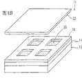
图1A是根据本发明例1的一个电子发射装置10的透视图。如图1A中所示,该电子发射装置10包括设置在一个衬底12上的电子发射阴极14,一个设置在电子发射阴极14上的绝缘膜16,及一个设置在绝缘膜16上由导电膜构成的栅极18。该栅极18及绝缘膜16两者都具有孔20。每个孔20最好其直径或在横向上具有约几毫微米至几十微米的尺寸。图1A中所示的孔20具有矩形形状,但也20可具有任何种类的形状,即圆形,三角形,五边形等。FIG. 1A is a perspective view of an electron-emitting
该电子发射装置10还包括一个阳极22,它对衬底12保持约几毫微米到几十微米的距离并使其置于栅极18的对面。阳极22与电子发射阴极14之间的内空间为约10-2至10-5乇的真空。利用在电子发射阴极14及栅极18之间施加几十至几百伏的电压及在电子发射阴极14及阳极22之间施加几百至几千伏的电压,施加在电子发射阴极14及栅极18之间的电压将使电子从电子发射阴极14的表面发射出来。大部分发射出的电子朝向阳极22发射,而一些发射出的电子进入到栅极18。可以利用施加于栅极18的电压调整被发射电子的量。The
虽然在图1A中所示的电子发射装置10具有三个端子,但也可以应用并提供仅具有两个端子的电子发射装置10。在此情况下,省掉了栅极18及绝缘膜16,由此使电子发射阴极14直接地与阳极22对置。换一种方式,如图1B所示,可将栅极18直接形成在电子发射阴极14上。在此情况下,当电流从电子发射阴极14经过孔20发射时,一部分电子将在栅极18及电子发射阴极14之间流过。Although the
图2是电子发射阴极14的一个透视图。如图2中所示,电子发射阴极14由碳膜24构成,在其中加有金刚石颗粒26。该金刚石颗粒26是p型导电性的。至少一些金刚石颗粒26部分地从碳膜24的表面中突出来。最好金刚石颗粒26的表面以氢原子为限界,由此使表面的电导率改善。FIG. 2 is a perspective view of the
电子通常在碳膜内部迁移。当电场通过碳膜24施加到金刚石颗粒26的表面上时,在碳膜24内部的电子转移到金刚石颗粒26的表面能级。金刚石天生具有非常小的电子亲和力,因此适于作电子发射材料。尤其是,金刚石的(111)面具有负的电子亲和力,并在该(111)面上其真空能级低于导带能级。其结果是,在金刚石颗粒26表面能级上的电子通过(111)面的导带能级发射到真空中。Electrons normally migrate within the carbon film. When an electric field is applied to the surface of the
电子发射到真空中是由于负的电子亲和力,因此不需要施加高的电压,并以大的转移几率发生。因而,非常大数目的电子可用非常低的电压发射。再者,这种电子发射机构不需要传统电子发射装置所需的高真空度。该电子发射装置10可在仅约10-2至10-5乇的真空度下发射电子。Emission of electrons into the vacuum is due to negative electron affinity, thus does not require application of high voltage and occurs with a large probability of transfer. Thus, a very large number of electrons can be emitted with a very low voltage. Furthermore, this electron emission mechanism does not require the high vacuum required by conventional electron emission devices. The
该电子发射装置10例如是用以下方法制造的。This
首先,在衬底12上形成电子发射阴极14。将具有p型导电性的金刚石颗粒与碳的细粉末相混合,对其添加合适的溶剂,以便形成糊剂。该金刚石颗粒26的颗粒直径最好在几毫微米至几微米的范围中。然后,在衬底12上由该糊剂形成合适厚度的膜并进行烘焙,以致得到碳膜24。在形成碳膜24时使其厚度小于金刚石颗粒26的颗粒直径,可保证金刚石颗粒26部分地从碳膜24的表面突出来。利用烧结处理,由于原子能级的结合或原子的相互作用在碳膜24的碳及金刚石颗粒26之间形成了表面能级。因此,电子从碳膜24移动到金刚石颗粒26中变得容易了。First, an
衬底12可以是任何材料,只要它具有的热阻能使衬底12在烧结处理期间免于其变型即可;它可以是导电的或绝缘的。也可以在另一衬底上用上述方法形成碳膜24,并然后将碳膜24转移到衬底12上。The
接着,将绝缘膜16及栅极18形成在由碳膜24作成的电子发射阴极16上。该绝缘膜16可由诸如氧化硅或氮化硅材料或其它的绝缘材料作成。导电膜18由导电材料如铝作成。Next, the insulating
然后,穿过栅极18及绝缘膜16形成孔20,以使电子发射阴极14的表面曝露出来。Then, a
最后,设置阳极22使其放置在电子发射阴极14的对面。将阳极22及电子发射阴极14之间的内空间密封住并使其保持真空状态,或者用另一方式,使整个阳极22及电子发射阴极14保持在真空中。于是就完成了电子发射装置10。可使用用于传统电子发射装置的导电元件,如形成在玻璃衬底上的透明电极,具有低电阻的硅衬底等来作阳极22。Finally, the
虽然在上例中是对碳膜添加了具有p型导电性的金刚石颗粒,但也可以使用任何材料作成的膜,只要它能使电子有效地注入到p型导电性的金刚石颗粒中就行。Although diamond particles having p-type conductivity are added to the carbon film in the above example, a film made of any material can be used as long as it can efficiently inject electrons into the diamond particles of p-type conductivity.
图3是由在其中添加了金刚石颗粒26的半导体膜30作成的电子发射阴极14的透视图。尤其是,该半导体膜30是被称为DLC(金刚石状的碳)的n型或赝n型非晶碳膜,它被掺入氮及包含微小的金刚石颗粒。该DLC膜具有的维氏硬度约为2000至6000kg/mm2,并且可由Raman散射频谱中1550cm-1及1240cm-1附近的特定宽峰来识别。词“赝n型”定义为虽然具有由电子组成的带隙及载流子但具有很小或不具有n型特性。FIG. 3 is a perspective view of an
在使用半导体膜30的情况下,最好在铝衬底32上形成半导体膜30,以便对半导体膜30提供电子。在使用铝时,在半导体膜30及衬底32之间获得一种欧姆接触。In the case of using the semiconductor film 30, it is preferable to form the semiconductor film 30 on the aluminum substrate 32 so as to supply electrons to the semiconductor film 30. When aluminum is used, an ohmic contact is obtained between the semiconductor film 30 and the substrate 32 .
利用结合上述结构的电子发射阴极14,对p型金刚石颗粒提供电子甚至可变得更容易,以致可在低电压下发射大量的电子。With the
利用在衬底32上分散金刚石颗粒26,及然后在该衬底32上形成半导体膜30(由n型DLC膜构成)可实现将金刚石颗粒26加到半导膜30中。也可以首先在衬底32上形成半导体膜30(由DLC膜构成),再将金刚石颗粒26压入半导体膜30,然后烘焙该半导膜30。The incorporation of the
该DLC膜例如可用以下方法形成。This DLC film can be formed, for example, by the following method.
将吡啶(pyridine)蒸气导入到排除了空气的真空室中。也可以将一惰性气体扩散到吡啶中并将其导入到一个室中。接着,对室内部的吡啶施加几十至几百伏的电压以使蒸发的吡啶电离,并以几千伏的电压使电离粒子加速及使其沉积在装在室内部的一个衬底上。由于该沉积膜包括氮原子,该膜的功能如一种n型半导体。也可以用哒嗪(pyridazine)及嘧啶(pyrimidine)或它们的衍生物来取代吡啶。也可以使用溶解在一种溶剂如苯中的吡嗪(pyrazine),1,3,5-三嗪(triazine)或它们的衍生物。Pyridine vapor was introduced into a vacuum chamber from which air was excluded. It is also possible to diffuse an inert gas into pyridine and introduce it into a chamber. Next, a voltage of several tens to several hundreds of volts is applied to the pyridine inside the chamber to ionize the evaporated pyridine, and the ionized particles are accelerated and deposited on a substrate housed inside the chamber at a voltage of several thousand volts. Since the deposited film includes nitrogen atoms, the film functions as an n-type semiconductor. Pyridazine and pyrimidine or their derivatives may also be used instead of pyridine. It is also possible to use pyrazine, 1,3,5-triazine or their derivatives dissolved in a solvent such as benzene.
如上所述,在根据本例的电子发射阴极中,金刚石颗粒被分散在一个碳膜或一个n型半导体膜上,以使它能够以印刷或类似方式形成。因此,可以容易地及以低成本地生产大面积的电子发射阴极。再者,因为电子从一平状面发射出来,电极不容易受损变坏。该与传统的机构不同的电子发射机构可使得在低的真空度下发射电子。此外,可以通过对在单位电极区域中的金刚石颗粒数目的控制方便地控制被发射电子的数量。与传统电子发射阴极相比可获得明显增大的单位面积的电流。As described above, in the electron emission cathode according to this example, diamond particles are dispersed on a carbon film or an n-type semiconductor film so that it can be formed by printing or the like. Therefore, a large-area electron emission cathode can be produced easily and at low cost. Furthermore, since the electrons are emitted from a flat surface, the electrodes are not easily damaged and deteriorated. This electron emission mechanism, which is different from the conventional mechanism, enables emission of electrons at a low degree of vacuum. In addition, the number of emitted electrons can be conveniently controlled by controlling the number of diamond grains in a unit electrode area. Compared with the traditional electron emission cathode, a significantly increased current per unit area can be obtained.
虽然在上述例中使用DLC膜作为半导体膜30,但也可使用由另外的半导体材料如硅或锗等作成的膜。【例2】Although a DLC film is used as the semiconductor film 30 in the above example, a film made of another semiconductor material such as silicon or germanium may also be used. 【Example 2】
图4A表示根据本发明例2的电子发射装置40的透视图。如图4A中所示,该电子发射装置40包括设在衬底42上的电子发射阴极44,设在电子发射阴极44上的绝缘膜46,及设在绝缘膜46上的栅极48。栅极48及绝缘膜46两者均具有孔50。电子发射阴极44的部分在孔50的底部上曝露出来。FIG. 4A shows a perspective view of an electron-emitting
该电子发射装置40还包括一个阳极22,它被保持在孔50中的电子发射阴极44的对面。在阳极22及电子发射阴极44之间的内空间是约为10-2至10-5乇的真空。利用在电子发射阴极44及栅极48之间施加几十至几百伏的电压及在电子发射阴极44及阳极22之间施加几百至几千伏的电压,施加在电子发射阴极44及栅极48之间的电压引起电子从电子发射阴极44的表面发射出来。大部分被发射出的电子流向阳极22,而一些被发射的电子进入到栅极48。利用对施加在栅极48上电压的调节可以调节被发射电子的量。The
图4B是该电子发射阴极44的横截面图。电子发射阴极44包括一个导电膜52,形成在该导电膜52上的n型半导体膜54,及形成在n型半导体膜54上的岛状p型半导体膜56。FIG. 4B is a cross-sectional view of the
虽然电子发射装置40在图4A及4B中被表示为具有三个端子,但是也可提供具有仅为两个端子的电子发射装置40。在此情况下,省略了栅极48及绝缘膜46,由此使电子发射阴极44直接与阳极对置,如图5中所示。另外,如图4C中所示,栅极48可直接形成在电子发射阴极14上。在此情况下,当电流从电子发射阴极44通过孔50发射时,一部分电子将在栅极48及电子发射阴极44之间流过。Although the
以下将描述根据本例的电子发射装置40的工作。The operation of the
当一n型半导体与一p型半导体彼此形成接触时,载流子将在结面上从高密度侧向低密度侧扩散。其结果是,在结面附近载流子消失,因此在热平衡状态时在n型半导体及p型半导体之间出现扩散势位。假定该扩散势位的值为e VD,则p型半导体的下端具有的能级比n型半导体的下端的能级高e VD。因此,变成p型半导体中少数载流子的电子注入到导带中,从能量利用来说使由p型半导体的导常发射电子比由n型半导体的导带发射电子更为有利。When an n-type semiconductor and a p-type semiconductor come into contact with each other, carriers will diffuse from the high-density side to the low-density side on the junction. As a result, carriers disappear in the vicinity of the junction, so that a diffusion potential appears between the n-type semiconductor and the p-type semiconductor in a thermal equilibrium state. Assuming that the value of this diffusion potential is e VD , the lower end of the p-type semiconductor has an energy level higher by e VD than the energy level of the lower end of the n-type semiconductor. Therefore, electrons that become minority carriers in the p-type semiconductor are injected into the conduction band, making electron emission from the conduction band of the p-type semiconductor more favorable than electron emission from the conduction band of the n-type semiconductor in terms of energy utilization.
图6是在相对阳极22将负电压施加到导电膜52的情况下电子发射阴极44的能常概图。FIG. 6 is an energy profile of the
导电膜52,n型半导体膜54及p型半导体膜56具有它们各自的费米能级62,64及66,如图6所示,在p型半导体膜56的一端与真空能级之间形成了一个垫垒68。
由于在阳极22和导电膜52之间施加了电压,电子70从导电膜52注入到n型半导体膜54的导带。也由于该施加的电压,电子70被注入到p型半导体膜56的导带中,该导带具有较高的能级。如上所述,在p型半导体膜56中电子亲和力似乎变得小于n型半导体膜54的导带中的亲和力。其结果是,注入到p型半导体膜56中的电子70穿过势垒68被释放到真空中,该势垒是由真空能级形成的但是由于施加电压而变得薄一些,并且电子被阳极22捕获。Due to the voltage applied between the
作为p型半导体膜56中少数载流子的电子70的状态是很重要的。在某些情况下,在p型半导体膜56的导带中的电子70是由p型半导体膜56的价带及p型半导体膜56的表面能级由于热能或类似能激励产生的;在另外情况下,在p型半导体膜56的导带中的电子是由n型半导体膜54注入的。为了阻止p型半导体膜56中的电子70通过与空穴72的再结合而消失(后者是p型半导体膜56中的多数载流子),当电子被释放到真空中时,电子70流经p型半导体膜56的迁移长度应小于电子70在p型半导体膜56中的扩散长度。因而,在pN结中n型半导体膜54及p型半导体膜56的薄层彼此附着的情况下,p型半导体膜56的厚度应被减小,以便避免上述问题。但是,均匀地产生非常薄的膜是困难的。因此,根据本例的电子发射装置的特点是局部地积沉在n型半导体膜54上的岛状p型半导体膜56。The state of
图7是表示该n型半导体膜54及p型半导体膜56之间的结的放大横截面图。厚度W小于电子70的扩散长度的情况下,电子70将如轨迹76所示地穿过p型半导体膜56而被释放。FIG. 7 is an enlarged cross-sectional view showing the junction between the n-
另一方面,在厚度W大于电子70的扩散长度的情况下,将难于沿图7中所示轨迹76释放电子70。但是,在pN结74的附近,由n型半导体膜54注入的电子70可以扩散到p型半导体膜56的表面。如轨迹80所示,已经扩散到p型半导体膜56表面的电子70在其与p型半导体膜56中的空穴再结合前变得可以被释放到真空中。某些类型的半导体用来构成p型半导体膜56能使电子70在p型半导体膜56的表面流过并如轨迹78所示地由p型半导体膜56的表面被释放出去。轨迹76,78及80意在作为示范的轨迹,电子释放的真实路径将不一定流过这些轨迹。On the other hand, in the case where the thickness W is greater than the diffusion length of the
因此,根据本例,部分地积沉在n型半导体膜上的p型半导体膜保证电子亲和力有所减小,由此使经过p型半导体膜扩散的电子易于达到p型半导体膜的表面。其结果是,能有效地发射电子。Therefore, according to the present example, the p-type semiconductor film partially deposited on the n-type semiconductor film ensures that electron affinity is reduced, thereby making it easy for electrons diffused through the p-type semiconductor film to reach the surface of the p-type semiconductor film. As a result, electrons can be efficiently emitted.
以下将参照图4A,4B及5描述制造该电子发射装置40的示范方法。An exemplary method of manufacturing the
首先,在衬底42上形成电子发射阴极44。在衬底42上形成导电膜52,及在导电膜52上形成n型半导体膜54。然后,在短时间中在n型半导体膜54上积沉p型半导体膜56,这将不能使p型半导体膜56整体地覆盖住n型半导体膜54。另一种方式是,形成整体覆盖n型半导体膜54的p型半导体层,然后利用有选择的蚀刻去除一部分p型半导体层,使得留下岛状p型半导体膜56。还可以使用具有岛状孔的掩摸在n型半导体膜54上形成p型半导体层再除去掩摸,或是在n型半导体膜54的表面上散布细的粒状p型半导体来获得p型半导体膜56。最好是将p型半导体膜56作成具有约几毫微米至几微米尺寸的岛。对导电膜52及n型半导体膜54进行选择,以使得在它们之间产生欧姆接触,并使得电子从导电膜52注入到n型半导体膜54变得容易。这样,就形成了电子发射阴极44。n型半导体膜54及p型半导体膜可以是由掺过硼,磷或氮的金刚石或DLC膜来形成。First, an
在电子发射阴极44上形成绝缘膜46及栅极48。该绝缘膜46可由氧化硅,氮化硅或类似物,及其它绝缘材料构成。栅极48由导电材料如铝构成。然后穿过栅极48及绝缘膜46形成孔50,以使得电子发射阴极44的表面被曝露出来。在形成图5中所示结构的电子发射装置的情况下,不需要形成栅极与绝缘膜46。An insulating
最后,将阳极设置成与电子发射阴极44相对置。阳极22及电子发射阴极之间的内空间被密封起来,以致保持真空状态,或用另一方式,使整个阳极22及电子发射阴极44保持在真空中。这样,就完成了该电子发射装置40。Finally, the anode is disposed opposite to the
如以下所描述的,可以获得上例所述电子发射阴极44的各种变型。Various modifications of the
图8概要地表示电子发射阴极80的横截面图。该电子发射阴极80包括形成在衬底42上的导电膜82,形成在导电膜82上的岛状n型半导体膜84,及形成在导电膜82上的岛状p型半导体膜86,并且后者成为局部地与n型半导体膜84相重叠。岛状n型半导体膜84及岛状p型半导体膜86可使用与上述电子发射阴极44所用方法相同的方法来形成。FIG. 8 schematically shows a cross-sectional view of the
电子发射阴极80当其替代电子发射阴极44被构在如图4A或5所示的电子发射装置40中时可类似地发射电子。The
由于n型半导体膜84及p型半导体膜86之间的界面曝露在表面上,经过n型半导体膜84内部或表面在p型半导体膜86内扩散的电子能容易地到达界面附近的p型半导体膜86的表面。因为p型半导体膜86具有似电子亲和力,它在p型半导体膜86被施加电压时小于n型半导体膜84的亲和力,故电子能有效地从p型半导体膜86的表面释放出来。Because the interface between the n-
在图9中所示的电子发射阴极90包括形成在衬底42上的一个导电膜92,形成在导电膜92上的岛状n型半导体膜94,及形成在n型半导体膜94上的p型半导体膜96。这种结构是由:形成覆盖整个导电膜92的n型半导体层,在n型半导体层上形成岛状p型半导体膜96,及使用p型半导体膜96作为掩模对n型半导体层进行蚀刻由此产生岛状n型半导体膜而获得的。The
该电子发射阴极90当其替代电子发射阴极44被结合在如图4A或5所示的电子发射装置40中时可类似地发射电子。This
因为n型半导体膜94及p型半导体膜96之间的界面被曝露在表面上,经过n型半导体膜94内部或表面在p型半导体膜96内扩散的电子能容易地到达界面附近的p型半导体膜96的表面。因为p型半导体膜96具有似电子亲和力,它在p型半导体膜96被施加电压时小于n型半导体膜94的亲和力,故电子能有效地从p型半导体膜96的表面释放出来。Because the interface between the n-
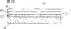
在图10中所示的电子发射阴极100包括形成在衬底42上的导电膜102,形成在导电膜102上的n型半导体膜104,及形成在n型半导体膜104上的p型半导体膜106,该p型半导体膜106具有孔108。具有孔108的p型半导体膜106可通过形成n型半导体膜104并使其覆盖整个导电膜102,形成限定孔108的岛状掩模,然后在n型半导体膜104上形成p型半导体膜106,再利用提起方法取走掩模来获得。The
该电子发射阴极100当其替代电子发射阴极44被结合在如图4A或5所示的电子发射装置40中时可类似地发射电子。This
因为n型半导体膜104及p型半导体膜106之间的界面被曝露在表面上,经过n型半导体膜104内部或表面在p型半导体膜106内扩散的电子能容易地到达界面附近的p型半导体膜106的表面。因为p型半导体膜106具有似电子亲和力,它在p型半导体膜106被施加电压时小于n型半导体膜104的亲和力,故电子能有效地从p型半导体膜106的表面释放出来。Because the interface between the n-
在图11中所示的电子发射阴极110包括形成在衬底42上的导电膜112,形成在导电膜112上的n型半导体膜114,及形成在n型半导体膜114上的p型半导体膜116,该n型半导体膜114及p型半导体膜具有多个孔118。导电膜112部分地在孔118的底部曝露出来。通过用光刻胶的蚀刻,阳极氧化或类似方法可以形成孔118。通过用光刻胶的蚀刻,可以形成其孔直径为微米(um)级的孔118。利用阳极氧化,可以形成其孔直径为毫微米(nm)级的孔118。对于孔118的直径及数目没有专门的限制。The electron emission cathode 110 shown in FIG. 11 includes a conductive film 112 formed on a
该电子发射阴极110当其替代电子发射阴极44被结合在如图4A或5所示的电子发射装置40中时,可类似地发射电子。The electron emission cathode 110 can similarly emit electrons when it is incorporated in the
因为n型半导体膜114及p型半导体膜116之间的界面被曝露在表面上,经过n型半导体膜114内部或表面在p型半导体116内扩散的电子能容易地到达界面附近的p型半导体膜116的表面。因为p型半导体膜116具有似电子亲和力,它在p型半导体膜116被施加电压时小于n型半导体膜114的亲和力,故电子能有效地从p型半导体膜116的表面释放出来。Because the interface between the n-type semiconductor film 114 and the p-type semiconductor film 116 is exposed on the surface, the electrons diffused in the p-type semiconductor 116 through the inside of the n-type semiconductor film 114 or the surface can easily reach the p-type semiconductor near the interface. surface of the membrane 116 . Since the p-type semiconductor film 116 has an electron-like affinity which is smaller than that of the n-type semiconductor film 114 when a voltage is applied to the p-type semiconductor film 116, electrons can be efficiently released from the surface of the p-type semiconductor film 116.
如上所述,本例的电子发射阴极具有这样的结构,其中电子从n型半导体膜中提供,及在n型半导体膜及p型半导体膜之间的结的附近被曝露在真空中。其结果是,从n型半导体膜注入到p型半导体膜的电子将沿在其与p型半导体膜中的空穴再结合前就能释放到真空中的路径移动。因此,电子能有效地从p型半导体膜中释放出来,该p型半导体膜与n型半导体膜相比具有较小的电子亲和力。As described above, the electron emission cathode of this example has a structure in which electrons are supplied from the n-type semiconductor film, and the vicinity of the junction between the n-type semiconductor film and the p-type semiconductor film is exposed to vacuum. As a result, electrons injected from the n-type semiconductor film to the p-type semiconductor film move along paths that can be released into vacuum before they recombine with holes in the p-type semiconductor film. Therefore, electrons can be efficiently released from the p-type semiconductor film, which has a smaller electron affinity than the n-type semiconductor film.
此外,不需要用突出形状的电子发射部分。因此,电子发射阴极可以形成在各种类型的衬底上,并且易于形成具有大面积的电子发射阴极。因为没有突出的部分,就不容易引起电场的聚集,由此随着时间电极的状态仅产生非常小的变化。In addition, there is no need to use the protruding shape of the electron-emitting portion. Therefore, an electron emission cathode can be formed on various types of substrates, and it is easy to form an electron emission cathode having a large area. Because there are no protruding parts, it is not easy to cause a concentration of an electric field, thereby producing only a very small change in the state of the electrode over time.
虽然在上述例中是在衬底42上形成导电膜,但如果衬底42本身是导电的,则不需要在衬底42上形成导电膜。也可以使用n型半导体衬底,并将衬底及n型半导体膜看成一个整体单元。Although the conductive film is formed on the
使用掺硼的金刚石作p型半导体将会产生更为有效的电子发射装置,如例1中所述因为相对另外的材料金刚石的电子亲和力非常小;及金刚石的某些晶体面具有负的电子亲和力。这种电子发射装置也可工作在低真空度(约10-2乇)中,因为金刚石对大气是惰性的,而硅基电子发射装置需要一定的真空度,因为它在大气中易受到污染,即,因为会形成氧化膜。最好是金刚石的表面以氢原子为限界,以便在金刚石表面获得优良的导电性能。The use of boron-doped diamond as a p-type semiconductor will result in more efficient electron emission devices, as described in Example 1, because diamond has a very low electron affinity relative to other materials; and certain crystal faces of diamond have negative electron affinity . This electron emission device can also work in a low vacuum (about 10-2 Torr), because diamond is inert to the atmosphere, and a silicon-based electron emission device requires a certain degree of vacuum, because it is easily polluted in the atmosphere, That is, because an oxide film is formed. Preferably, the diamond surface is bounded by hydrogen atoms in order to obtain good electrical conductivity on the diamond surface.
使用金刚石作n型半导体膜看来是可能的,但难以获得具有满意特性的n型金刚石。因此,最好如例1中所述的,使用包括小金刚石颗粒的DCL膜作为n型半导体膜。在此情况下,铝适于作导电膜,以致能获得极佳的欧姆接触。It seems possible to use diamond as an n-type semiconductor film, but it is difficult to obtain n-type diamond with satisfactory characteristics. Therefore, as described in Example 1, it is preferable to use a DCL film including small diamond particles as the n-type semiconductor film. In this case, aluminum is suitable as a conductive film so that an excellent ohmic contact can be obtained.
此外,在上述的电子发射阴极中,n型半导体膜形成在导电膜上及p型半导体膜形成在n型半导体膜上。但是电子发射阴极也可包括形成在导电膜上的p型半导体膜及形成在p型半导体膜上的n型半导体膜。这是因为p-n结曝露在真空气氛中便带来了本发明的某些效果。【例3】Furthermore, in the above-mentioned electron emission cathode, the n-type semiconductor film is formed on the conductive film and the p-type semiconductor film is formed on the n-type semiconductor film. However, the electron emission cathode may also include a p-type semiconductor film formed on the conductive film and an n-type semiconductor film formed on the p-type semiconductor film. This is because some effects of the present invention are brought about by exposing the p-n junction to the vacuum atmosphere. 【Example 3】
在本例中,将描述包括例1及例2中所述的电子发射阴极或电子发射装置的平板显示器。In this example, a flat panel display including the electron emission cathode or electron emission device described in Example 1 and Example 2 will be described.
图12A是平板显示器150的横截面概图。虽然,图12A所描绘的例中使用的是例2中所述的电子发射阴极(见图5),但是在例1及2中所述的任何电子发射阴极均可用于该平板显示器150。FIG. 12A is a schematic cross-sectional view of a
在该平板显示器150中,如例2中所述的包括一个导电膜52,一个n型半导体膜54及一个p型半导体膜56的电子发射阴极44被形成在一个支承衬底152上。In the
该平板显示器150还包括一个由玻璃或类似物作成的透明衬底156。由ITO(铟锡氧化物)或类似物作成的透明电极158形成在透明衬底156上,在该透明电极上设有荧光膜160。该荧光膜160是由无机材料如ZnO∶Zn或有机材料如荧光染料及一种荧光导电聚合物构成的。The
透明衬底156及支承衬底152彼此保持一定距离,在它们之间夹有绝缘体154,以使得透明电极158与电子发射阴极44彼此对置。在透明衬底156及支承衬底152之间形成的内空间162中是真空。The
利用在该平板显示器150的透明电极158及电子发射阴极44之间施加电压,电子将从电子发射阴极44中释放出来并被加速。被加速的电子与透明电极158上的荧光膜160相撞击且荧光膜受激励,由此发光。By applying a voltage between the
在该平板显示器150中,当一个加速装置设置于电子发射阴极44及透明衬底156之间来取代透明电极150的情况中,可以省掉透明电极150。在此情况下,最好在荧光膜160上设置一层薄铝膜。In the
也可以设置栅极48来拉出靠近电子发射阴极44的电子,如图12B中所示的平板显示器170内那样。栅极48设置在电子发射阴极44上并在它们之间夹有绝缘膜46。如参照图4在例2中所解释的,栅板48可直接地形成在电子发射阴极44上。在图12B中也曾出现在图12A中的构件使用与其中相同的标号。在平板显示器170中,利用在栅极48及电子发射阴极44之间施加电压使电子从电子发射阴极44中拉出,并被透明电极158(它是阳极)加速,以使得透明电板158上的荧光膜160受激励,由此发光。A
在图12A中的平板显示器具有两个端子,因此具有简单的结构。图12B中的平板显示器170具有三个端子,因此它具有相对复杂的结构,但是由于它的栅板,有利于灰色色调的显示器。The flat panel display in FIG. 12A has two terminals and thus has a simple structure. The
为了能构成具有多个象素的平板显示器,可以使用如13中所示结构的电子发射阴极。图13是表示相对于一个象素的电子发射阴极结构的透视图。如图13中所示,条状信号电极线180作成沿着方向Y延伸,并有如例1或例2中所述的电子发射阴极设置在该条状栅极线180上。另外,延X方向延伸的条状栅极线182形成在信号电极线180上,因此与信号电极线180相交叉并在它们之间夹有绝缘膜184。在栅极线182及信号电极线180的交叉处,有一个孔186形成在栅极线182中,由此使电子发射阴极44的表面曝露出来。如果需要的话,可以在不与栅极线182交叉的电子发射阴极44的部分设置绝缘膜。In order to be able to construct a flat panel display having a plurality of pixels, an electron emission cathode having a structure as shown in 13 can be used. Fig. 13 is a perspective view showing the structure of an electron emission cathode with respect to one pixel. As shown in FIG. 13, the strip-shaped
利用多个信号电极线180及多个栅极182按上述结构布置,以致构成一个其上设有一象素矩阵的衬底,并将该衬底放置在带有设了荧光膜的透明电极的对面,便可实现具有多个象素的平板显示器。【例4】Utilize a plurality of
如例1及2中所述的,本发明的电子发射阴极能在真空中高效地发射大量电子。利用这个特点,可以实现具有一种新颖结构的热电式冷却装置。As described in Examples 1 and 2, the electron emission cathode of the present invention can efficiently emit a large amount of electrons in a vacuum. Utilizing this feature, a thermoelectric cooling device with a novel structure can be realized.
图14表示一种热电式冷却装置200的横截面概图。该热电式冷却装置200包括第一导电衬底202,形成在该第一导电衬底202上的阴极204,及第二导电衬底206。在例1及2中所述的任何一种电子发射阴极均可用作阴极204,第一导电衬底202及第二导电衬底206布置成彼此对置并使阴极204面向内。在第一导电衬底202及第二导电衬底之间的空间210中是用密封玻璃208密封的真空。第一导电衬底202与第二导电衬底206之间的间隙保持在约100um或更小。FIG. 14 shows a schematic cross-sectional view of a
利用在第二衬底206上施加电压并使第一导电衬底202处于负电位,来自电源的电子从第一导电衬底202移向阴极204。在该时间点上,由于珀尔贴(peltier)效应第一导电衬底202将吸热。By applying a voltage across the
如例1或例2所述的,阴极204能高效率地将电子发射到真空中。因此,第一导电衬底202流入阴极204的电子被吸出到真空210中,由于电子发射效应使第一导电衬底202或阴极204失去热。As described in Example 1 or Example 2, the
被发射的电子在吸出到真空210中后进入到与第一导电衬底202对置的第二导电衬底206。在此时刻,电子以热释放了它们自己的位能及动能,因而使第二导电衬底206受加热。The emitted electrons enter the second
因此,当操作热电式冷却装置200时,第一导电衬底202被冷却,而第二衬底206被加热。因为导电衬底202及206放置在真空210中,该真空210阻止热量从第二衬底206传送到第一衬底202,由此就阻止了由于热漏损产生的冷却或加热效率的任何实质性下降。被从第一导电衬底202取走的热量愈大及施加的吸出电子的电压愈高则热效应愈大。Thus, when
于是,就获得了一种高效率及大功率的热电式冷却装置。因为电极可由金属板及薄膜作成,故不需要如在传统的珀尔贴元件的情况中那样使用大量稀有金属,表现出资源有效使用的优点。由于仅需要小量的相应材料,该装置可作成具有小重量,并导致低的制造成本。由于真空的空间可设计成很窄,可以实现非常薄的冷却装置。Thus, a high-efficiency and high-power thermoelectric cooling device is obtained. Since the electrodes can be made of metal plates and thin films, there is no need to use a large amount of rare metals as in the case of conventional Peltier elements, exhibiting an advantage of efficient use of resources. Since only a small amount of corresponding material is required, the device can be made with low weight, resulting in low manufacturing costs. Since the vacuum space can be designed to be very narrow, a very thin cooling device can be realized.
如以下所述的,可作出对这种热电式冷却装置的各种改型。Various modifications to this thermoelectric cooling device can be made, as described below.
如图15所示的热电式冷却装置220包括一个阴极226,它取代图14中所示的热电式冷却装置200的阴极204。该阴极226包括一个n型半导体膜222及形成在n型半导体膜222表面上的氧化铯膜224。此外,该热电式冷却装置220包括形成在第二导电衬底206面上的阳极236,该阳极与第一导电衬底202相对置。阳极236包括p型半导体膜236及氧化铯膜234。The
因为氧化铯具有小的逸出功,故上述结构能以高效率将电子释放到真空中。通过构成具有相反导电型的阴极226的半导体膜222及阳极236的半导体膜232(即分别为n型及p型),可以减低第一导电衬底202及第二导电衬底206之间所施加的电压。此外,利用使电流流动方向反向,可以变为使第二导电衬底206冷却及使第一导电衬底202加热。Since cesium oxide has a small work function, the above structure can release electrons into vacuum with high efficiency. By forming the
表示在图16中的热电式冷却装置240包括一个n型半导体膜242,它取代图15中所示的热电式冷却装置220的阴极226,及一个p型半导体膜246,它取代热电式冷却装置220中的阳极236。该n型半导体膜242在其表面上具有多个微小的突起244。该p型半导体膜246在其表面上也具有多个微小的突起244。The
根据上述结构,甚至在使用具有相对大逸出功的半导体材料时也可以释放大量电子到真空中。According to the above structure, even when a semiconductor material having a relatively large work function is used, a large amount of electrons can be released into a vacuum.
该微小突起244可以直接地形成在n型半导体膜242及p型半导体膜246上。另一方式是,可以在第一导电衬底202及第二导电衬底206上形成微小突起,然后在它们各自表面上形成n型半导体膜242及p型半导体膜246。The
也可以对该热电式冷却装置的外部结构进行改型。It is also possible to modify the external structure of the thermoelectric cooling device.
图17中所示的热电式冷却装置300包括一个起第一导电衬底作用的圆筒形导体302,设置在该圆筒形导体302表面的阴极304,起第二导电衬底作用的一个圆筒形导体306,及设置在该圆筒形导体306内壁面上的阳极308。圆筒形导体306布置成与圆筒形导体302相共轴。The thermoelectric cooling device 300 shown in Fig. 17 comprises a cylindrical conductor 302 which acts as a first conductive substrate, a cathode 304 which is arranged on the surface of the cylindrical conductor 302, and a circular conductor which acts as a second conductive substrate. A cylindrical conductor 306 and an anode 308 disposed on the inner wall of the cylindrical conductor 306 . The cylindrical conductor 306 is arranged coaxially with the cylindrical conductor 302 .
任何参照图15及16所描述的阴极及阳极可用来作为相应的阴极304及阳极308。也可以使用在例1及2中所述的任何电子发射阴极来作电子发射阴极304,而省掉阳极308。Any of the cathodes and anodes described with reference to FIGS. 15 and 16 may be used as the cathode 304 and anode 308, respectively. It is also possible to use any of the electron emission cathodes described in Examples 1 and 2 as the electron emission cathode 304, and to omit the anode 308.
利用密封件312将圆筒形导体302及圆筒形导体306固定住,并使其保持真空310。在圆筒形导体302的内壁面及圆筒形导体306的外壁面上分别设有多个肋片314及316。The cylindrical conductor 302 and the cylindrical conductor 306 are fixed by a seal 312 and kept in a vacuum 310 . A plurality of ribs 314 and 316 are respectively disposed on the inner wall of the cylindrical conductor 302 and the outer wall of the cylindrical conductor 306 .
从电源流出的电子进入圆柱形导体302,并当其移到形成在圆柱形导体302表面的阴极304时,由于珀尔贴效应而吸热。该吸热效应对于绕肋片314流动的流体作功,因此该流体失去热,即被冷却。另一方面,由于在圆筒形导体306及圆筒形导体302之间施加了电压,进入阴极304的电子被从阴极304的表面拉出,在真空310中飞行,穿过阳极308并进入到圆筒形导体306,这时电子将释放它们保留的能量,这使得圆筒形导体306被加热。辐射热将通过肋片316传送并到达在肋片316外侧流动的流体,于是使该流体加热。根据这种结构,甚至当其作得非常紧凑时也可使流体被高效地冷却或加热。Electrons flowing from the power source enter the cylindrical conductor 302, and when they move to the cathode 304 formed on the surface of the cylindrical conductor 302, absorb heat due to the Peltier effect. This heat absorption effect does work on the fluid flowing around the fins 314 so that the fluid loses heat, ie is cooled. On the other hand, due to the voltage applied between the cylindrical conductor 306 and the cylindrical conductor 302, the electrons entering the cathode 304 are pulled from the surface of the cathode 304, fly in the vacuum 310, pass through the anode 308 and enter the The cylindrical conductor 306, the electrons will then release their retained energy, which causes the cylindrical conductor 306 to be heated. The radiant heat will be transmitted through the fins 316 and reach the fluid flowing outside the fins 316, thereby heating the fluid. According to this structure, the fluid can be efficiently cooled or heated even when it is made very compact.
圆筒形导体302及306也可具有任何形状,只要它们分别能起到第一导电衬底及第二导电衬底的作用,尽管圆筒形状能提供更好的热效率。例如,圆筒导体302及306也可具有多边形状,以取代圆筒形状。Cylindrical conductors 302 and 306 may also have any shape as long as they function as first and second conductive substrates, respectively, although cylindrical shapes provide better thermal efficiency. For example, the cylindrical conductors 302 and 306 may also have a polygonal shape instead of a cylindrical shape.
可以理解,根据本例的热电式冷却装置,加热件及冷却件彼此被小真空内空间隔开,因此大大地降低了从高温侧到低温侧的热量漏损。因为该真空内腔非常的小,故由于空间电荷效应出现的电子屏障是很小的。因此,电子的发射能有效地进行。在使用了例1或例2中所述的高效率电子发射阴极的情况下,由于电子发射效应可获得显著的冷却效果。其结果是,可以实现重量轻、效率高及功率大的热电式冷却装置。It can be understood that, according to the thermoelectric cooling device of this example, the heating element and the cooling element are separated from each other by a small vacuum inner space, thus greatly reducing the heat leakage from the high temperature side to the low temperature side. Because the vacuum cavity is very small, the electron barrier due to space charge effect is very small. Therefore, emission of electrons can be efficiently performed. In the case where the high-efficiency electron-emitting cathode described in Example 1 or Example 2 is used, a remarkable cooling effect can be obtained due to the electron-emitting effect. As a result, a lightweight, efficient and powerful thermoelectric cooling device can be realized.
虽然对例3及4所述的平板显示器及热电式冷却装置作为例1及2中所述的电子发射装置的应用例作出描述,但本发明的电子发射阴极及电子发射装置也可应用于工作于高速度的一种开关装置。Although the flat panel display and the thermoelectric cooling device described in Examples 3 and 4 are described as application examples of the electron emission device described in Examples 1 and 2, the electron emission cathode and electron emission device of the present invention can also be applied to work. A switching device for high speed.
因此,根据本发明,提供了一种电子发射阴极及一种电子发射装置,它们可相对地免于时效的损坏,允许构成大面积的装置,并甚至在低真空度时也能高效地发射电子并且成本低及是有优异的批量生产率。并且,提供了包括该电子发射电极的一种高亮度、长寿命及大型显示的平板显示器。Therefore, according to the present invention, there are provided an electron emission cathode and an electron emission device which are relatively free from aging damage, allow construction of a large-area device, and efficiently emit electrons even at a low degree of vacuum. And the cost is low and there is excellent mass production rate. And, there is provided a high-brightness, long-life and large-scale display flat panel display including the electron emission electrode.
另外,也提供了一种包括该电子发射电极的一种重量轻、效率高及功率大的热电式冷却装置。In addition, a light-weight, high-efficiency and high-power thermoelectric cooling device including the electron emission electrode is also provided.
在不偏离本发明的精神和范围的情况下对于熟悉本领域的技术人员显然易于作出各种另外的变更。因此所附权利要求书的范围并不仅局限于所给出的说明上,而应具有较宽的结构。Various additional modifications will be apparent to those skilled in the art without departing from the spirit and scope of this invention. Therefore, the scope of the appended claims should not be limited to the description given, but should have a broader construction.
Claims (22)
Translated fromChineseApplications Claiming Priority (6)
| Application Number | Priority Date | Filing Date | Title |
|---|---|---|---|
| JP24122194 | 1994-10-05 | ||
| JP241221/1994 | 1994-10-05 | ||
| JP5601695 | 1995-03-15 | ||
| JP056016/1995 | 1995-03-15 | ||
| JP060755/1995 | 1995-03-20 | ||
| JP6075595 | 1995-03-20 |
Related Parent Applications (1)
| Application Number | Title | Priority Date | Filing Date |
|---|---|---|---|
| CN95118252ADivisionCN1080923C (en) | 1994-10-05 | 1995-10-05 | Electron emission cathode, method of manufacturing the same, and application thereof |
Publications (2)
| Publication Number | Publication Date |
|---|---|
| CN1282974Atrue CN1282974A (en) | 2001-02-07 |
| CN1146002C CN1146002C (en) | 2004-04-14 |
Family
ID=27295780
Family Applications (2)
| Application Number | Title | Priority Date | Filing Date |
|---|---|---|---|
| CN95118252AExpired - Fee RelatedCN1080923C (en) | 1994-10-05 | 1995-10-05 | Electron emission cathode, method of manufacturing the same, and application thereof |
| CNB001054570AExpired - Fee RelatedCN1146002C (en) | 1994-10-05 | 1995-10-05 | Electron emitting cathode and its manufacturing method and application |
Family Applications Before (1)
| Application Number | Title | Priority Date | Filing Date |
|---|---|---|---|
| CN95118252AExpired - Fee RelatedCN1080923C (en) | 1994-10-05 | 1995-10-05 | Electron emission cathode, method of manufacturing the same, and application thereof |
Country Status (4)
| Country | Link |
|---|---|
| US (2) | US5777427A (en) |
| EP (1) | EP0706196B1 (en) |
| CN (2) | CN1080923C (en) |
| DE (1) | DE69515245T2 (en) |
Families Citing this family (47)
| Publication number | Priority date | Publication date | Assignee | Title |
|---|---|---|---|---|
| US5698328A (en)* | 1994-04-06 | 1997-12-16 | The Regents Of The University Of California | Diamond thin film electron emitter |
| KR100405886B1 (en)* | 1995-08-04 | 2004-04-03 | 프린터블 필드 에미터스 리미티드 | Electron emission material, method of manufacturing the same, and device using a net |
| KR100442982B1 (en)* | 1996-04-15 | 2004-09-18 | 마츠시타 덴끼 산교 가부시키가이샤 | Field-emission electron source and method of manufacturing the same |
| JP3547588B2 (en)* | 1997-03-10 | 2004-07-28 | パイオニア株式会社 | Electron emitting element and display device using the same |
| DE19727606A1 (en)* | 1997-06-28 | 1999-01-07 | Philips Patentverwaltung | Electron emitter with nanocrystalline diamond |
| US6181056B1 (en)* | 1997-10-21 | 2001-01-30 | Si Diamond Technology, Inc. | Cold cathode carbon film |
| KR100377284B1 (en)* | 1998-02-09 | 2003-03-26 | 마쯔시다덴기산교 가부시키가이샤 | Electron emitting device and method of producing the same |
| JP3131782B2 (en)* | 1998-12-08 | 2001-02-05 | キヤノン株式会社 | Electron emitting element, electron source and image forming apparatus |
| JP2000182508A (en)* | 1998-12-16 | 2000-06-30 | Sony Corp | Field emission type cathode, electron emitting device, and manufacture of electron emitting device |
| US6172448B1 (en) | 1999-01-29 | 2001-01-09 | Motorola, Inc. | Method and apparatus for utilizing heat dissipated from an electrical device |
| GB2346731B (en)* | 1999-02-12 | 2001-05-09 | Toshiba Kk | Electron emission film and filed emission cold cathode device |
| JP3323848B2 (en) | 1999-02-26 | 2002-09-09 | キヤノン株式会社 | Electron emitting element, electron source using the same, and image forming apparatus using the same |
| GB9905132D0 (en)* | 1999-03-06 | 1999-04-28 | Smiths Industries Plc | Electron emitting devices |
| US6664722B1 (en)* | 1999-12-02 | 2003-12-16 | Si Diamond Technology, Inc. | Field emission material |
| US6783589B2 (en)* | 2001-01-19 | 2004-08-31 | Chevron U.S.A. Inc. | Diamondoid-containing materials in microelectronics |
| US6911768B2 (en)* | 2001-04-30 | 2005-06-28 | Hewlett-Packard Development Company, L.P. | Tunneling emitter with nanohole openings |
| KR100786832B1 (en)* | 2001-08-29 | 2007-12-20 | 삼성에스디아이 주식회사 | Negative pattern printing method using cross printing method and field emission display device having gate hole formed by this method |
| US6949873B2 (en)* | 2002-03-08 | 2005-09-27 | Chien-Min Sung | Amorphous diamond materials and associated methods for the use and manufacture thereof |
| US20070126312A1 (en)* | 2002-03-08 | 2007-06-07 | Chien-Min Sung | DLC field emission with nano-diamond impregnated metals |
| US20080029145A1 (en)* | 2002-03-08 | 2008-02-07 | Chien-Min Sung | Diamond-like carbon thermoelectric conversion devices and methods for the use and manufacture thereof |
| US7235912B2 (en)* | 2002-03-08 | 2007-06-26 | Chien-Min Sung | Diamond-like carbon thermoelectric conversion devices and methods for the use and manufacture thereof |
| US7358658B2 (en)* | 2002-03-08 | 2008-04-15 | Chien-Min Sung | Amorphous diamond materials and associated methods for the use and manufacture thereof |
| US6806629B2 (en) | 2002-03-08 | 2004-10-19 | Chien-Min Sung | Amorphous diamond materials and associated methods for the use and manufacture thereof |
| US7085125B2 (en)* | 2002-03-21 | 2006-08-01 | Chien-Min Sung | Carbon nanotube devices and uses therefor |
| JP2003317606A (en)* | 2002-04-19 | 2003-11-07 | Mitsubishi Pencil Co Ltd | Electrode for electron gun and electron gun |
| KR100469391B1 (en)* | 2002-05-10 | 2005-02-02 | 엘지전자 주식회사 | Driving circuit for mim fed and driving method thereof |
| GB2389959B (en)* | 2002-06-19 | 2006-06-14 | Univ Dundee | Improved field emission device |
| JP3851861B2 (en)* | 2002-09-20 | 2006-11-29 | 財団法人ファインセラミックスセンター | Electron emitter |
| ITTO20030167A1 (en)* | 2003-03-06 | 2004-09-07 | Fiat Ricerche | PROCEDURE FOR THE CREATION OF NANO-STRUCTURED EMITTERS FOR INCANDESCENT LIGHT SOURCES. |
| US20070003472A1 (en)* | 2003-03-24 | 2007-01-04 | Tolt Zhidan L | Electron emitting composite based on regulated nano-structures and a cold electron source using the composite |
| US20050019955A1 (en)* | 2003-07-23 | 2005-01-27 | Dahl Jeremy E. | Luminescent heterodiamondoids as biological labels |
| CN100424905C (en)* | 2003-10-07 | 2008-10-08 | 松下电器产业株式会社 | Thermoelectric conversion element, method for manufacturing same, cooling device using thermoelectric conversion element, and method for controlling cooling device |
| US8102108B2 (en)* | 2003-12-05 | 2012-01-24 | Zhidan Li Tolt | Low voltage electron source with self aligned gate apertures, fabrication method thereof, and devices using the electron source |
| US7312562B2 (en)* | 2004-02-04 | 2007-12-25 | Chevron U.S.A. Inc. | Heterodiamondoid-containing field emission devices |
| US7305839B2 (en) | 2004-06-30 | 2007-12-11 | General Electric Company | Thermal transfer device and system and method incorporating same |
| US7260939B2 (en) | 2004-12-17 | 2007-08-28 | General Electric Company | Thermal transfer device and system and method incorporating same |
| US7498507B2 (en) | 2005-03-16 | 2009-03-03 | General Electric Company | Device for solid state thermal transfer and power generation |
| KR20060122336A (en)* | 2005-05-26 | 2006-11-30 | 삼성에스디아이 주식회사 | Electron emission display device having a cooling device and the fabrication method for thereof |
| KR20070017758A (en)* | 2005-08-08 | 2007-02-13 | 삼성에스디아이 주식회사 | Field emission device and manufacturing method thereof |
| KR100708717B1 (en) | 2005-10-11 | 2007-04-17 | 삼성에스디아이 주식회사 | Electron emitting light emitting device and flat panel display device using the same |
| US7741764B1 (en) | 2007-01-09 | 2010-06-22 | Chien-Min Sung | DLC emitter devices and associated methods |
| CN101471214B (en)* | 2007-12-28 | 2010-06-16 | 中国航天科技集团公司第五研究院第五一〇研究所 | A kind of diamond thin film solar cell and preparation method thereof |
| US8018053B2 (en)* | 2008-01-31 | 2011-09-13 | Northrop Grumman Systems Corporation | Heat transfer device |
| KR20090095301A (en)* | 2008-03-05 | 2009-09-09 | 삼성에스디아이 주식회사 | Flat panel display apparatus |
| CN103695863B (en)* | 2013-12-09 | 2016-04-13 | 四川大学 | The preparation method of a kind of boron-doped diamond film/carbon film combination electrode material |
| CN105047504B (en)* | 2015-07-14 | 2017-05-03 | 中国科学院苏州生物医学工程技术研究所 | Field emission cathode based on two-dimensional nanowall |
| CN109301045B (en)* | 2018-10-19 | 2020-07-31 | 京东方科技集团股份有限公司 | A light-emitting device, preparation method thereof, and display device |
Family Cites Families (19)
| Publication number | Priority date | Publication date | Assignee | Title |
|---|---|---|---|---|
| US3808477A (en)* | 1971-12-17 | 1974-04-30 | Gen Electric | Cold cathode structure |
| US4276440A (en)* | 1978-04-07 | 1981-06-30 | Pierino Cannelli | Thermoelectric generator operating with a cooling device for converting solar energy into electric energy, and system for the use thereof |
| US4382833A (en)* | 1981-08-25 | 1983-05-10 | Rca Corporation | Vacuum lamination fixture |
| US4513308A (en)* | 1982-09-23 | 1985-04-23 | The United States Of America As Represented By The Secretary Of The Navy | p-n Junction controlled field emitter array cathode |
| NL8400297A (en)* | 1984-02-01 | 1985-09-02 | Philips Nv | Semiconductor device for generating an electron beam. |
| US5019003A (en)* | 1989-09-29 | 1991-05-28 | Motorola, Inc. | Field emission device having preformed emitters |
| JP2936174B2 (en)* | 1990-04-20 | 1999-08-23 | 松下電器産業株式会社 | Electronic components |
| WO1991017601A1 (en)* | 1990-05-02 | 1991-11-14 | Fitzgerald David J | Energy converter |
| JP3255960B2 (en)* | 1991-09-30 | 2002-02-12 | 株式会社神戸製鋼所 | Cold cathode emitter element |
| US5199918A (en)* | 1991-11-07 | 1993-04-06 | Microelectronics And Computer Technology Corporation | Method of forming field emitter device with diamond emission tips |
| US5252833A (en)* | 1992-02-05 | 1993-10-12 | Motorola, Inc. | Electron source for depletion mode electron emission apparatus |
| US5278475A (en)* | 1992-06-01 | 1994-01-11 | Motorola, Inc. | Cathodoluminescent display apparatus and method for realization using diamond crystallites |
| JPH0613664A (en)* | 1992-06-29 | 1994-01-21 | Matsushita Electric Ind Co Ltd | Thermoelectric device and method for manufacturing thermoelectric device |
| US5410166A (en)* | 1993-04-28 | 1995-04-25 | The United States Of America As Represented By The Secretary Of The Air Force | P-N junction negative electron affinity cathode |
| US5578901A (en)* | 1994-02-14 | 1996-11-26 | E. I. Du Pont De Nemours And Company | Diamond fiber field emitters |
| US5637950A (en)* | 1994-10-31 | 1997-06-10 | Lucent Technologies Inc. | Field emission devices employing enhanced diamond field emitters |
| US5623180A (en)* | 1994-10-31 | 1997-04-22 | Lucent Technologies Inc. | Electron field emitters comprising particles cooled with low voltage emitting material |
| US5709577A (en)* | 1994-12-22 | 1998-01-20 | Lucent Technologies Inc. | Method of making field emission devices employing ultra-fine diamond particle emitters |
| US5869922A (en)* | 1997-08-13 | 1999-02-09 | Si Diamond Technology, Inc. | Carbon film for field emission devices |
- 1995
- 1995-10-02DEDE69515245Tpatent/DE69515245T2/ennot_activeExpired - Fee Related
- 1995-10-02EPEP95115520Apatent/EP0706196B1/ennot_activeExpired - Lifetime
- 1995-10-05USUS08/539,699patent/US5777427A/ennot_activeExpired - Fee Related
- 1995-10-05CNCN95118252Apatent/CN1080923C/ennot_activeExpired - Fee Related
- 1995-10-05CNCNB001054570Apatent/CN1146002C/ennot_activeExpired - Fee Related
- 1998
- 1998-03-24USUS09/047,131patent/US5984752A/ennot_activeExpired - Fee Related
Also Published As
| Publication number | Publication date |
|---|---|
| US5984752A (en) | 1999-11-16 |
| DE69515245D1 (en) | 2000-04-06 |
| US5777427A (en) | 1998-07-07 |
| CN1146002C (en) | 2004-04-14 |
| EP0706196A2 (en) | 1996-04-10 |
| EP0706196B1 (en) | 2000-03-01 |
| CN1138208A (en) | 1996-12-18 |
| DE69515245T2 (en) | 2000-07-13 |
| CN1080923C (en) | 2002-03-13 |
| EP0706196A3 (en) | 1996-08-21 |
Similar Documents
| Publication | Publication Date | Title |
|---|---|---|
| CN1146002C (en) | Electron emitting cathode and its manufacturing method and application | |
| CN100341094C (en) | Method for enhancing field emission, emitter, transistor, display and light emitting device | |
| JP3537053B2 (en) | Electron source for electron emission device | |
| CN1103110C (en) | Field electron emission materials and devices | |
| CN1282210C (en) | Field emission electron source, its production method and display using said electron source | |
| CN1207745C (en) | Electron emission element, electronic source and image forming device | |
| CN1066285C (en) | Image-forming apparatus | |
| CN1574159A (en) | Method of manufacturing electron-emitting device, method of manufacturing electron source, and method of manufacturing image display device | |
| CN1279563C (en) | Image display device and its mfg. method | |
| CN1148774C (en) | Field emission type electron source and its manufacturing method | |
| CN101060048A (en) | Electron-emitting device, electron source, image display apparatus and method of fabricating electron-emitting device | |
| CN1205512C (en) | Pattern, wiring, circuit board, electron source and image forming device mfg. method | |
| CN1202545C (en) | Planar electron-emitting device, display using same, and method for emitting electrons | |
| CN1574155A (en) | Electron emission device, electron source, and image display having dipole layer | |
| CN1828816A (en) | display board | |
| CN100337299C (en) | Phosphor light-emitting element, manufacturing method thereof, and image drawing device | |
| CN1640202A (en) | Light-emitting element, production method thereof, and display device | |
| CN1639822A (en) | Transmitting type secondary electron surface and electron tube | |
| JP3187302B2 (en) | Electron emission cathode, electron emission element, flat display, and thermoelectric cooling device using the same, and method of manufacturing electron emission cathode | |
| CN101055898A (en) | Photoelectric conversion device, photoelectric conversion element, substrate thereof, and manufacturing method | |
| CN1090802C (en) | Cathode for electron tube | |
| CN1271676C (en) | Plate display and its manufacturing method | |
| CN1828815A (en) | display board | |
| JP2002343278A (en) | Display device and display device manufacturing method | |
| JPH07226148A (en) | Semiconductor electron emitting element |
Legal Events
| Date | Code | Title | Description |
|---|---|---|---|
| C10 | Entry into substantive examination | ||
| SE01 | Entry into force of request for substantive examination | ||
| C06 | Publication | ||
| PB01 | Publication | ||
| C14 | Grant of patent or utility model | ||
| GR01 | Patent grant | ||
| C19 | Lapse of patent right due to non-payment of the annual fee | ||
| CF01 | Termination of patent right due to non-payment of annual fee |