CN1282143A - Power amplification circuit with load regulator for controlling adjacent and alternate channel power - Google Patents
Power amplification circuit with load regulator for controlling adjacent and alternate channel powerDownload PDFInfo
- Publication number
- CN1282143A CN1282143ACN00121347ACN00121347ACN1282143ACN 1282143 ACN1282143 ACN 1282143ACN 00121347 ACN00121347 ACN 00121347ACN 00121347 ACN00121347 ACN 00121347ACN 1282143 ACN1282143 ACN 1282143A
- Authority
- CN
- China
- Prior art keywords
- power
- average
- peak
- output
- signal
- Prior art date
- Legal status (The legal status is an assumption and is not a legal conclusion. Google has not performed a legal analysis and makes no representation as to the accuracy of the status listed.)
- Granted
Links
- 230000003321amplificationEffects0.000titleclaimsdescription34
- 238000003199nucleic acid amplification methodMethods0.000titleclaimsdescription34
- 238000000034methodMethods0.000claimsdescription19
- 230000004044responseEffects0.000claimsdescription12
- 230000008859changeEffects0.000claimsdescription8
- 239000003990capacitorSubstances0.000description11
- 238000005070samplingMethods0.000description11
- 238000012935AveragingMethods0.000description10
- 238000012360testing methodMethods0.000description10
- 230000001413cellular effectEffects0.000description8
- 238000010586diagramMethods0.000description7
- 230000005540biological transmissionEffects0.000description6
- 238000005516engineering processMethods0.000description6
- 238000001514detection methodMethods0.000description4
- 238000005259measurementMethods0.000description4
- 238000001228spectrumMethods0.000description4
- 230000001276controlling effectEffects0.000description3
- 230000006870functionEffects0.000description3
- 238000013459approachMethods0.000description2
- 230000002457bidirectional effectEffects0.000description2
- 230000003139buffering effectEffects0.000description2
- 238000006243chemical reactionMethods0.000description2
- 238000004891communicationMethods0.000description2
- 230000007423decreaseEffects0.000description2
- 230000003247decreasing effectEffects0.000description2
- 238000002955isolationMethods0.000description2
- 230000008569processEffects0.000description2
- 230000005855radiationEffects0.000description2
- 230000015572biosynthetic processEffects0.000description1
- 239000002131composite materialSubstances0.000description1
- 230000008878couplingEffects0.000description1
- 238000010168coupling processMethods0.000description1
- 238000005859coupling reactionMethods0.000description1
- 238000013461designMethods0.000description1
- 230000005611electricityEffects0.000description1
- 230000008030eliminationEffects0.000description1
- 238000003379elimination reactionMethods0.000description1
- 238000002474experimental methodMethods0.000description1
- 230000005669field effectEffects0.000description1
- 238000001914filtrationMethods0.000description1
- 238000012986modificationMethods0.000description1
- 230000004048modificationEffects0.000description1
- 239000003607modifierSubstances0.000description1
- 230000010363phase shiftEffects0.000description1
- 238000011084recoveryMethods0.000description1
- 230000001105regulatory effectEffects0.000description1
- 230000000630rising effectEffects0.000description1
- 239000004065semiconductorSubstances0.000description1
- 230000008054signal transmissionEffects0.000description1
- 230000003595spectral effectEffects0.000description1
- 238000003786synthesis reactionMethods0.000description1
- 238000012546transferMethods0.000description1
- 238000013519translationMethods0.000description1
Images


Classifications
- H—ELECTRICITY
- H03—ELECTRONIC CIRCUITRY
- H03F—AMPLIFIERS
- H03F3/00—Amplifiers with only discharge tubes or only semiconductor devices as amplifying elements
- H03F3/20—Power amplifiers, e.g. Class B amplifiers, Class C amplifiers
- H—ELECTRICITY
- H03—ELECTRONIC CIRCUITRY
- H03F—AMPLIFIERS
- H03F1/00—Details of amplifiers with only discharge tubes, only semiconductor devices or only unspecified devices as amplifying elements
- H03F1/02—Modifications of amplifiers to raise the efficiency, e.g. gliding Class A stages, use of an auxiliary oscillation
- H03F1/0205—Modifications of amplifiers to raise the efficiency, e.g. gliding Class A stages, use of an auxiliary oscillation in transistor amplifiers
- H—ELECTRICITY
- H03—ELECTRONIC CIRCUITRY
- H03F—AMPLIFIERS
- H03F1/00—Details of amplifiers with only discharge tubes, only semiconductor devices or only unspecified devices as amplifying elements
- H03F1/32—Modifications of amplifiers to reduce non-linear distortion
- H03F1/3241—Modifications of amplifiers to reduce non-linear distortion using predistortion circuits
Landscapes
- Engineering & Computer Science (AREA)
- Power Engineering (AREA)
- Physics & Mathematics (AREA)
- Nonlinear Science (AREA)
- Amplifiers (AREA)
- Transmitters (AREA)
- Control Of Amplification And Gain Control (AREA)
Abstract
Description
The application relate to by the title of the applications such as Alberth for the series number of " load envelope following amplifier system " for _ _ (No.CS10069) and by the title of David Schlueter application for the series number of " having power supply and adjusting to control adjacent and power amplifier alternate channel power " for _ _ (No.CS10158) and by the title of the applications such as Klomsdorf for the series number of " based on the amplifier load regulating system of memory " for _ _ (No.CS10022) and the pendent U.S. Patent application of the title of being applied for by Alberth etc. as the series number of " load envelope elimination and recovery amplifier system " as (No.CS90026).
The present invention relates generally to power amplifier.More particularly, the present invention relates to be used to improve the power amplifier circuit of efficient and adjacent channel power.
Power amplifier is a key technology in the portable radiotelephone design.In cell phone, power amplifier has very big influence to the permissible call time.This is because with respect to other circuit in cell phone inside, the power of the remarkable quantity of power amplifier consumption.The parameter how much power the definition power amplifier consumes is an efficiency power amplifier.
For the efficient in the preset range that improves incoming signal level, its direct current supply voltage continuously changes so that normally known with the power amplifier of signal level demand coupling.The title that is presented to Thomas R.Apel in June 11 nineteen eighty-two has disclosed such example for the U.S. Patent No. 4442407 of " being used for two loop automatic electric-levels controls of power amplifier ".' 407, response is corresponding to the comparison between the amplitude of the signal of the weighted sum of the amplitude of power amplifier load current and supply power voltage and modulation signal, and the modulation by radio frequency amplifier direct current supply voltage is with improved efficient operand power amplifier.
Yet this disclosed system does not but relate to another important performance characteristic of cell phone system intermediate power amplifier, i.e. Fa She adjacent and alternate channel power in ' 407.In cell phone system, the adjacent channel power of radiation may cause interference in other honeycomb channel, thereby causes the decline of overall system performance.In the cellular system that uses such as the linear modulation scheme of interim standard (IS)-136 time division multiple access (TDMA) and IS-95 code division multiple access (CDMA), adjacent and alternate channel power parameter are more crucial.By irrespectively optimizing the efficient of power amplifier with adjacent and alternate channel power performance, this power amplifier can not reach the power standard of the adjacent and alternate channel that is used for specific cellular system.
The method of a kind of linearity that increases power amplifier simultaneously and efficient is presented to the No.5 of the title of Yukio Ikeda etc. for " linear amplifier " in December 1 nineteen ninety, discloses in 101,172 the United States Patent (USP).In ' 172, so that follow the amplitude leyel of output signal, but this has increased the efficient of power amplifier has also introduced amplitude modulation (AM) and phase modulation (PM) distortion drain voltage by a DC/DC transducer control.Therefore, collaborative phase place and amplitude comparator use the input and output envelope detector together and offset the distortion of being introduced by power amplifier so that introduce predistortion.Native system requires the distortion of accurate tracking power amplifier, and this may be very difficult.In addition, when a plurality of couplers and phase/amplitude comparison circuit are used in the portable cell phone, size and cost have been increased.
The technology of power amplifier distortion minimization that makes another kind is presented to the title of Shingo Kamiya for disclosing in the U.S. Patent No. 4,348,644 of " power amplification circuit with supply power voltage modifier " on March 24th, 1980.' 644, the crest factor of the output signal of power amplification circuit detection power amplifier (for example peak to average ratio).When crest factor was big, the supply power voltage of power amplifier was raised.On the contrary, when crest factor is hour, supply power voltage is lowered.Thereby so that when handling high peak to average ratio, supply power voltage is raised when the supply power voltage of the high power amplifier of needs.On the contrary, when being little peak to average ratio here, supply power voltage is lowered.Therefore believe by the rising supply power voltage and can reproduce peak value, and reduce power loss by the supply power voltage that raises and reduce power amplifier as required.
In the electronic system of amplifying music signal, ' 644 technology are of great use.In this class was used, for gratifying fidelity is provided, the accurate reproduction of music signal was essential.Yet for cost portable radiotelephone effectively and efficiently is provided, ' 644 technology can not satisfy its essential fidelity and the coordination between the efficient.
Therefore, power amplifier need provide the more accurate and control widely to the adjacent and alternate channel power of being launched by power amplifier.Further needing of power amplifier is to adopt the linear modulation scheme operation effectively.The power amplifier of use in portable radiotelephone needs a kind of method of coordinating linear and efficient.Here also need to arrive component change, come control power amplifiers adjacent channel power, alternate channel power and efficient performance by the parts that exist in the compensation portable antenna phone.In control power amplifiers linearity and efficient, also need the average transmit power of control power amplifiers.
Fig. 1 is a wireless telephonic block diagram with Receiver And Transmitter;
Fig. 2 is the block diagram that is used to carry out the testing apparatus of peak to average ratio test;
Fig. 3 be used for Fig. 2 testing apparatus in supply power voltage, gain and the peak-peak of finite time on the cycle to the curve of average power ratio with respect to input power;
Fig. 4 be used for Fig. 2 testing apparatus in adjacent channel power, alternate channel power and the peak-peak of finite time on the cycle to the curve of average power ratio with respect to input power;
Fig. 5 is to use the block diagram of a power amplification circuit in the transmitter of Fig. 1;
Fig. 6 is to use peak value in the power amplification circuit of Fig. 5 to the block diagram of mean value difference detector; With
Fig. 7 represents a kind of method of amplification RF signal;
Fig. 8 represents to be used to the variable impedance network in the power amplification circuit of Fig. 5;
Fig. 9 represents the second embodiment variable impedance network; With
Figure 10 is the impedance curve of variable impedance network.
Fig. 1 is the formal specification mobilephone communication system 100 with block diagram.This mobilephone communication system 100 comprisesremote transceiver 10 and one or more radio telephone such as radio telephone 12.Theportable radiotelephone 12 of thisremote transceiver 10 in designated geographic area sends the RF signal and theportable radiotelephone 12 in designated geographic area receives the RF signal.
Generally,user interface 26 comprises microphone, loud speaker, display and keypad.Thisuser interface 26 is used to receive user's input information and provides the reception data that transmitted by remote transceiver 10.Receiver 18 comprises all known in the prior art low noise amplifier, filter, down conversion mixer and orthogonal mixer, and the such circuit of automatic gain control circuit.
In order to launch the RF signal that comprises information fromradio telephone 12 toremote transceiver 10, thisuser interface 26 is directed to thiscontroll block 20 with user input data.Generally,controll block 20 comprises the DSP core, microcontroller core, memory, clock generating circuit, more any in software and the output power controllingcircuit.Controll block 20 is the information format that obtains fromuser interface 26 and send it totransmitter 16 so that be converted to the RFmodulation signal.Transmitter 16 is sent toantenna 14 so that be transferred toremote transceiver 10 with this RF modulation signal.Therefore,transmitter 16 is used to launch modulating information signal.Duplexer provides isolation between bytransmitter 16 emissions and the signal byreceiver 18 receptions.
At first, carry out the experiment of prototype power amplifier so that whether the emission peak of the signal of determining to be produced bytransmitter 16 can be used for predicting adjacent channel power and alternate channel power to the mean value ratio.Adjacent channel power is defined as, the quantity of power in the nominated bandwidth of launching in the channel that is being close totransmitter 16 channel of operation.Alternate channel power is defined as, the quantity of power in the nominated bandwidth of launching in surpassing the channel of two channels oftransmitter 16 channel of operation.
For example, in IS-95 cdma cellular telephone system, the emission function is operated on the 836MHz.This adjacent channel be 836MHz+/-885KHz, and alternate channel be 836MHz+/-1.98MHz.
Fig. 2 is the block diagram that is used to carry out the testing apparatus 200 of peak to average ratio test.Testing apparatus 200 comprises thesignal generator 40 that is coupled to the input of power amplifier element (DUT) 44 to be tested by bidirectional coupler 42.The output 56 of DUT44 is connected to coupler 46.
By DUT44 this RF input signal is amplified so that produce amplifying signal at DUT output 56, this amplifying signal is loaded into coupler 46 then.Through port 58 part of amplifying signal is coupled to spectrum analyzer 60.Utilize spectrum analyzer 60 can measure the adjacent channel power and the alternate channel power of this amplifying signal with respect to the power on the channel of operation.Through the remainder of wattmeter 68 measurements at the amplifying signal of coupler output 66 generations, and peak value and average power.
In each input power levels, measure emission adjacent and alternate channel power through spectrum analyzer 60.As known in the prior art, by on the switching regulaor (not shown), changing the supply power voltage that DUT44 is adjusted in pulse width modulation.Selectively, by using linear regulator also can adjust supply power voltage.
Fig. 3 be on the limited time cycle supply power voltage, DUT gain and maximum instantaneous peak to average ratio with respect to the curve of input power.The longitudinal axis 90 on the left side is the gain of representing with dB corresponding to the DUT44 of gain curve 92.The longitudinal axis 94 on the right is the supply power voltage of representing with volt corresponding to the DUT44 of supply voltage curve 96.The longitudinal axis 94 on the right also be the peak-peak represented with dB on the cycle of finite time to mean value than and corresponding to peak value-mean value curve 98.Transverse axis 102 is input powers of representing with dBm.
Fig. 3 explanation changes DUT44 on input power range supply power voltage is possible so that keep constant power output.Because the linear growth of input power by changing the supply power voltage of DUT, has linear decline in the gain of DUT44.
Peak value-mean value curve 98 is a peak-peak on designated time intervals curves to the mean value ratio.Utilize testing equipment to use peak value to keep measuring technique to detect the maximum instantaneous peak to average ratio of each input power and supply power voltage placement.For example, signal generator 40 (Fig. 2) produces the input signal of the OQPSK modulation with the similar IS-95CDMA of being used for cellular system.Therefore, the maximum instantaneous peak to average ratio of input signal is 5.2dB.When DUT44 is linear and does not introduce significant distortion, the maximum instantaneous peak to average ratio of measurement will approach 5.2dB.
(for example-9dBm) and the supply power voltage of 3.2V, peak value-mean value curve 98 shows that DUT44 is linear for low input power.By the maximum instantaneous peak to average ratio at-9dBm input record approximately is this true provable this point of 5.2dB; At low input power level place, DUT44 does not introduce distortion (for example, peak signal slicing).
In addition, peak value-mean value curve 98 shows when the input power of DUT44 and increases and the supply power voltage of DUT44 is adjusted so that when keeping constant power output the maximum instantaneous peak to average ratio monotone decreasing on the limited time cycle.Here, the peak to average ratio monotone decreasing represents that difference operation can be used in the control loop, so that in the retentive control loop stability, the maximum instantaneous peak to average ratio of the expectation on the limited time cycle is set.These results are applicable to various power outputs, are applicable to the different Designing power amplifier of using identical semiconductor device even are applicable to different power amplifier apparatus technology, such as field-effect transistor (FET) or bipolar transistor technology.
Fig. 4 is that adjacent channel power, alternate channel power and maximum instantaneous peak to average ratio on limited time cycle is with respect to the curve of input power.Keep constant at 20dBm again by changing the supply power voltage power output.
Thelongitudinal axis 112 on the left side is the alternate and adjacent channel power of representing with dBc of DUT44.Transverse axis 114 is input powers of representing with dBm.AdjCP_lowcurve 116 is the output adjacent channel powers on the downside of channel of operation.For example, the channel of operation of input signal is set to 836MHz.Then the adjacent channel power at downside is than the power in the 30kHz frequency bandwidth of the low 885kHz of 836MHz.Similarly, AdjCP_highcurve 118 is the output adjacent channel powers than the high 885kHz of 836MHz.
AltCP_lowcurve 120 is the output alternate channel powers than the low 1.98MHz of 836MHz.Similarly, AltCP_highcurve 122 is the output alternate channel powers than the high 1.98MHz of 836MHz.In Fig. 4, also shown corresponding to the adjacent channel power specification limit (Adj_speclimit curve 124 42dBc) and corresponding to the alternate channel power specification limit (Alt_speclimit curve 126 54dBc), the both is according to the IS-95CDMA standard.For its specification limit difference of different cellular standards.
Thelongitudinal axis 128 on the right is corresponding to the maximum instantaneous peak to average ratio on the limited time cycle of representing with dB of peak value-mean value curve 130.Peak value-mean value curve 130 is curves identical with the peak value of Fig. 3-mean value curve 98, because two curves are all represented identical data.
Power output keeps constant because input stimulus increases progressively, so adjacent channel power and alternate channel power increase progressively.Notice that be less than about greatly-situation of 55dBc for adjacent channel and alternate channel power, this measured value is limited by the limitation (for example, the spectral purity of the dynamic range of thespectrum analyzer 60 of Fig. 2 and signal generator 40) of test instrumentation., for approaching data point adjacent and alternate channel power and their the interlaced place of specification limit, adjacent channel and alternate channel power curve are dull.
The standard that meetszone 136 and alternate channel power near the standard of adjacent channel power meetszone 138, and the maximum instantaneous peak to average ratio on the limited time cycle is inversely proportional to alternate channel power with adjacent.Specific hereto DUT44 because input power increases progressively, had just reached the specification limit of adjacent channel power before the specification limit of alternate channel power reaches.Therefore, for specific power amplifier as DUT44, can monitor the maximum instantaneous peak to average ratio on the limited time cycle,, and will determine that the standard of alternate channel power meets so that adjust the adjacent channel power that supply power voltage obtains to expect.
Because can predictably control the maximum instantaneous peak to average ratio on the limited time cycle, equally also can control adjacent channel power.By control the maximum instantaneous peak to average ratio on the limited time cycle at the output of power amplifier, can control adjacent channel and alternate channel power indirectly.This provides the mode of the adjacent and alternate channel power of a kind of effective and predictable control.
For example, for the IS-95CDMA cellular system, the specification limit of adjacent channel power is-42dBc.Shown in dotted line 152, adjacent channel power strides across the maximum instantaneous peak to average ratio of the crosspoint 150 (Fig. 4) at specification limit place corresponding to the about 2.6dB on the limited time cycle.Therefore, comprise the transmitter of the power amplifier of DUT44 for use, the maximum instantaneous peak to average ratio on the limited time cycle remains on about 2.6dB so that make adjacent and the alternate channel power output remains within the standard.For some nargin are provided, power amplifier circuit can remain on 2.8dB or 3dB with the maximum instantaneous peak to average ratio on the limited time cycle.
Fig. 5 is to use the block diagram of the power amplification circuit 300 in transmitter 16 (Fig. 1).Power amplification circuit 300 comprises the power amplifier 172 that is coupled to variable impedance network 174.Envelope detector 178 is coupled to power amplifier output 173.In described embodiment, envelope detector 178 is coupled to the output of variable impedance network 174.Envelope detector 178 is coupled to peak value to average detector 180, and peak value is coupled to controller 184 to average detector 180 then.Alternatively, controller can be in controll block 20 (Fig. 1).Controller is coupled to variable impedance network 174.
Peak value comprises that to average detector the peak value that is coupled to analog-digital converter (ADC) 192 and digital circuit 194 is to mean value difference detector 182.Peak value comprises peak detector 186,averaging circuit 188 anddifference channel 190 to meanvalue difference detector 182.
By input 170 modulated RF input signal is loaded into power amplifier 172.Power amplifier 172 produces amplifying signal at output 174.The part of amplifying signal is coupled to envelope detector 178.
Envelope detector can be used as from amplifying signal eliminates the RF carrier signal.The gained signal is loaded into peak value to mean value difference detector 182.Peak value detects the average power of the peak level of amplifying signals and amplifying signal to meanvalue difference detector 182 and provides peak level on the predetermined period of time and the indication of average power.
Peak detector 186 is determined peak level, andaveraging circuit 188 is determined average power 188.Difference channel 190 determines that the difference between peak level and the average power is so that produce difference signal.Because sampling is the average value sample on the predetermined period of time, so this sampling occurs on the low rate.For example, for the IS-136TDMA cellular system, on the order of magnitude that occurs in about 150KHz of sampling (for example, mean value of each pulse train), and for CDMA Cellular System, on the order of magnitude that occurs in about 20KHz of sampling (mean value of per 50 μ sec).
Difference signal is loaded into ADC192 and is used to be converted to digital sampling, is also referred to as numeric word.In digital circuit 194, numeric word and difference correlation table 196 are compared.Therefore, to the mean value difference, produce the peak to average ratio of gained according to peak value by digital circuit 194.Digital circuit comprises traditional logical circuit well known in the prior art and state machine.Selectively, utilize digital signal processor (DSP) or microprocessor can realize the comparison of correlation table.
The peak to average ratio of gained is loaded into controller 184.In response to the peak level of amplifying signal and the indication of the difference between the average power, controller 184 produces load control signal, and is loaded into variable impedance network 174.In response to the peak level of amplifying signal and the indication of the difference between the average power (for example, in response to load control signal), variable impedance network 174 provides different impedances to arrive the output 173 of power amplifier.Adjust impedance that power amplifier output 173 presents till the peak level of the amplifying signal that occurs at output 176 and average power ratio equal predetermined level in fact.In other words, adjust this impedance and equal the peak to average ratio expected up to the peak to average ratio of reality in fact.By keeping the peak to average ratio of amplifying signal, power amplification circuit 300 is also controlled the adjacent channel power and the alternate channel power emission of radiation.
Alternatively, power amplification circuit 300 can comprise the circuit of controlling average output power.Average output power according to changeable expectation, the average output power of transmitter 16 (Fig. 1) changes, and controller makes variable impedance network 174 only present different impedances to power amplifier output 173 on the part of total dynamic range of average output power then.
Variable gain circuit here is a variable gain amplifier 206, input 170 is coupled to the input of power amplifier 172.Averaging circuit 188 produces indication on the circuit 191 of average output power.ADC192 is converted to digital signal with the indication of average output power, and digital circuit 194 is loaded into controller 184 with this digital signal then.Controller 184 produces the gain control signal that is loaded into VGA206 so that control the gain of VGA206, thereby keeps the average output power of expectation.
Fig. 6 is to the peak value of average detector 180 (Fig. 5) use and the embodiment ofdifference detector 182 with peak value.This peak value anddifference detector 182 compriseaveraging circuit 188, the firstoperational amplifiers 266,difference channel 190, peak detector 186 and secondoperational amplifier 272.
Be loaded into theinput 260 of peak value and difference detector by the envelope signal of envelope detector 178 (Fig. 5) generation.This envelope signal is loaded into averagingcircuit 188 and peak detector 186.Produce the peak value of envelope signal by peak detector 186, and produce the mean value of envelope signal by averagingcircuit 188.
Firstoperational amplifier 266 and secondoperational amplifier 272 are between averagingcircuit 188 and thedifference channel 190 and the voltage follower that isolation is provided between peak detector 186 and difference channel 190.The mean value of buffering is loaded into first input end 304, and the detection signal peak value of buffering is loaded into second input 306.Difference betweenoutput 262 generation peak values and average value signal.
In another embodiment of the power amplification circuit of Fig. 5, peak value anddifference detector 182 do not comprise difference channel 190.Replace, by ADC192, to peak detector 186 and averagingcircuit 188 direct samplings.Digital circuit 194 or controller 184 calculate peak to average ratio.Therefore this another embodiment has eliminated the needs to the circuit structure of correlation table 196 and simplification.For using single peak detector 186 and singleaveraging circuit 188 in the enough dynamic ranges on the 20dB order of magnitude, ADC192 must have high-resolution on the order of magnitude of 12 bits.
In another another embodiment of the power amplification circuit of Fig. 5, peak value does not comprise peak value anddifference detector 182 to average detector 180.Replace, the envelope signal via line 179 that is produced by envelope detector 178 directly is loaded into ADC192.Peak to average ratio is to utilize software to calculate.In the IS-136TDMA cell phone system, the ADC192 envelope signal of must on about 50KHz, sampling.For the IS-95CDMA cell phone system, the ADC192 envelope signal of must on about 2.5MHz, sampling.
When detection baseband signal that the ADC192 direct sampling is produced by envelope detector 178, power amplification circuit can comprise optional base-band digital peak detector 175 so that eliminate the needs of high sampling rate more.Transmitter 16 (Fig. 1) comprises the digital baseband circuit (for example as be known in the art, by encoder, not shown) that is used for receiving information signal and produces digital I-Q stream.Transmitter 16 (Fig. 1) further comprises the traditional transmitter circuitry (also not shown) that is used for digital stream is converted to radio frequency (RF) input signal as be known in the art.For example, transmitter circuitry comprises frequency translation frequency mixer, quadrature modulator and filter.
Digital peak wave detector 175 monitors the digital stream that is produced by the digital baseband circuit (not shown) through port one 71 and when occurs so that determine the peak value in the RF input signal.Digital peak wave detector 175 produces and is loaded into the peak value index signal that postpones square frame 181.Postponing square frame is that explanation is when the digital delaying circuit of digital stream by transmitter 16 (Fig. 1) and the delay that digital stream will experience when output 176 (Fig. 5) produces.This inhibit signal is loaded into the sampling of ADC192 and preserves circuit so that trigger ADC192 in the reasonable time sampled peak value.ADC192 produces digital peak then.
Digital peak wave detector 175 comprises the Digital Logic that can realize in the application-specific integrated circuit (ASIC) (ASIC).Digital peak wave detector 175 monitors that the envelope detector 178 that makes of IQ bit stream produces the known bit mode of priori of peak amplitude in envelope.Digital peak wave detector function can also be carried out by the software realization or by controller 184 (Fig. 5).Monitor digital baseband signal peak value example pendent title for the series number of " digital modulator " be with compensation No.08/694/004 application in 8 days Augusts in 1996 U.S. Patent application in describe, transfer assignee of the present invention, its content is comprised as a reference at this.
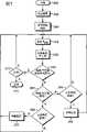
Fig. 7 represents to illustrate a kind of flow chart of method of amplification RF signal.This method originates insquare frame 350, opens atsquare frame 352 portable radiotelephone phones 12 (Fig. 1) then.Be set to initial impedance atsquare frame 354 variable impedance networks 174 (Fig. 5).For example, this can finish to variable impedance network 402 (Fig. 9) by sending numeric word 0000.Initial impedance is the known point impedance that rises, so that make the portable radiotelephone phone meet adjacent and the alternate channel power standard.
Atsquare frame 356, select the average power of expectation and the gain of VGA206 (Fig. 5) is set so that obtain the average power of expectation.Make the power output loop keep locking so that keep the average output power of expectation by the gain that constantly monitors average output power and adjustment VGA206 (Fig. 5).
Detect the peak to average ratio of amplifying signals atsquare frame 358, determine that indecisional block 360 peak to average ratio of these detections is whether within predetermined level or limit range then.If the peak to average ratio that detects is within predetermined level, then determine whether this method is finished (for example, whether the signal transmission is finished) in decisional block 372.If method is finished, then this method finishes atsquare frame 374; Otherwise this method proceeds tosquare frame 356.
Predetermined level is that known any one predetermined peak value corresponding to certain alternate channel radiant power and certain adjacent channel radiant power is to the mean value ratio.For example, in the IS-95CDMA portable radiotelephone, predetermined peak value may approximately be 3dB to the mean value ratio.
Determine indecisional block 360 whether this peak to average ratio (does not for example enough approach predetermined level, within predetermined level plus-minus predetermined value, such as+/-0.5dB within), whether the peak to average ratios of determining to detect indecisional block 362 greater than predetermined level then.If the peak to average ratio that detects is greater than predetermined level, then decisional block 364 determine variable impedance networks 174 (Fig. 5) whether oriented power amplifier output 173 (Fig. 5) present the more remaining impedance adjusting range of different impedances.
If (Fig. 5) do not have how available dynamic range from variable impedance network 174, then variable impedance network 174 keeps existing setting, and flow process proceeds to square frame 356.For example, be 1111 if be loaded into the current numeric word of variable impedance network 402 (Fig. 9), then there is not more upstate to rise to variable impedance network 174 (Fig. 5) here.
If more available dynamic range (for example current numeric word is less than 1111) is arranged, then change load control signal so that adjust variable impedance network 174 (Fig. 5) at square frame 366.For example,, adjustvariable impedance network 402, comprise increasing digital control word (for example, load control signal), for example from 1110 to 1111 to higher state for variable impedance network 402 (Fig. 9).This method proceeds tosquare frame 356 then.
If determine atsquare frame 362 peak to average ratio that detects is lower than predetermined level, determines atsquare frame 368 whether any remaining dynamic range is arranged so in variable impedance network 174 (Fig. 5).For example, if current in the load control signal of Fig. 9variable impedance network 402 be 0000, then load control signal can not be dropped to lower.If do not remain dynamic range, then keep the existing setting of variable impedance network 174 (Fig. 5), flow process proceeds tosquare frame 356 then.
If variable impedance network 174 (Fig. 5) has how available dynamic range, then change load control signal so that adjust variable impedance network 174 at square frame 370.For example,, adjust variable impedance network 174 and comprise for variable impedance network 402 (Fig. 9): reduce digital control word (for example load control signal) to a lower state, for example, from 0001 to 0000.Then, this method proceeds tosquare frame 356.
Fig. 8 represents the variable impedance network 400 that can be used for presenting to power amplifier 172 (Fig. 5) various impedances of first embodiment.Variable impedance network 400 comprises: first transmission line 408, be coupled to fixedly by-pass capacitor 412, the second transmission lines 410 of earth potential 416 and at least one is coupled to the variable element 418 of earth potential 416.Can from the combination that comprises variable capacitance diode and voltage-variable capacitor, select variable element 418.Load control signal is loaded into input 403 as voltage so that change the electric capacity of variable element 418.The impedance that arrow 404 explanations present at input 406 remains the optimum impedance of each output power levels of power amplifier 172 (Fig. 5) in fact.Controller 184 (Fig. 5) produces aanalogvoltage as load control signal.Therefore, controller can comprise that digital analog converter (DAC) is so that produce this analog signal.
Can envision other structure of variable impedance network 400.For example, add ons can comprise such as lamped element or element with distributed parameters inductance coil, additional transmission line and capacitor and additional variable element.
Fig. 9 represents thevariable impedance network 402 of second embodiment.Variable impedance network 402 comprises,first transmission line 442 is coupled to fixedly by-pass capacitor 446, thesecond transmission lines 444 ofearth potential 448 and at least one is coupled to the variable element 452 of earth potential 448.At least one variable element 452 comprises the output 173 (Fig. 5) that uses PIN diode or micro-machinery switch selectively to be coupled to power amplifier and a plurality ofcapacitors 454 that disconnect from the output 173 of power amplifier.Load control signal is loaded intoinput 450, so that a plurality ofswitches 456 of switch, these a plurality of switches are coupled to a plurality ofcapacitors 454 output 173 (Fig. 5) ofpower amplifier.Arrow 458 is illustrated in the impedance thatinput 440 presents and is held.
In described embodiment, controller 184 (Fig. 5) produces four digital bit control signals and controls a plurality of switches 456.Controller can comprise the shift register (not shown) so that digital control word is converted to four bit parallel words as load control signal.In another embodiment, shift register can with power amplifier 172 on a multi-chip module (Fig. 5).Therefore, forvariable impedance network 402, have 16 kinds of different impedances.
Therefore, variable impedance network has a variable element at least.Variable element can from comprise that variable capacitance diode, voltage-variable capacitor and use micro electromechanical switch or PIN diode selectively are coupled to the output of signal amplifier and the group of a plurality of capacitors of disconnecting from the output of signal amplifier select.
Do not need creative work just can expect other structure of variable impedance network 402.For example, Fu Jia element can comprise such as lamped element or element with distributed parameters inductance coil, additional transmission line and capacitor and additional variable element.The combination of variable impedance network 400 andvariable impedance network 402 can be used for increasing the scope of obtainable impedance.In addition, load control signal can comprise a plurality of signals of controlling different variable impedance elements respectively.
Figure 10 is the Smith chart 470 of expression impedance state scope, for example, and corresponding to variable impedance network 402 (Fig. 9).First impedance state 472 is also represented the initial impedance state, the load control signal corresponding to 0000.Last impedance state 474 is corresponding to 1111 load control signal.
The previous described first-selected embodiment that provides allows any technical staff of this area to make or uses to have the power amplification circuit that load is adjusted.Concerning those skilled in the art, will be conspicuous to the various modifications of these embodiment, and, can be loaded into other embodiment and needn't use creative ability in the general principle of this definition.For example, power amplification circuit can use with the transmitter on operating in a more than frequency band.Adjust load according to peak to average ratio and operational frequency bands (for example, the peak to average ratio of different expectations).
This power amplification circuit provides a kind of high-efficiency method of improving efficiency power amplifier when keeping essential adjacent channel and alternate channel power performance.Can obtain adjacent and alternate channel power from power amplifier in fact.Selectively, can from transmit path, obtain adjacent and alternate channel power by other transmitter circuitry in the power amplifier front.This power amplification circuit also consider the parts that in portable radiotelephone, occur on the component change to adjacent and control alternate channel power.
Claims (14)
1. power amplification circuit comprises:
Be used for amplification input signal so that produce the power amplifier of amplifying signal;
Be coupled to the variable impedance network of the output of power amplifier, in response to load control signal, this variable impedance network presents different impedances to the output of power amplifier;
The peak value of output that is coupled to power amplifier is to the mean value difference detector, and the average power that peak value detects the peak level of amplifying signal and amplifying signal to the mean value difference detector provides the indication of difference between peak level and the average power then; With
Be coupled to the controller of peak value to mean value difference detector and variable impedance network, in response to the peak level and the indication of the difference between the average power of amplifying signal, this controller is used to produce load control signal.
2. according to the power amplification circuit of claim 1, its middle controller make variable impedance network to the output of power amplifier present different impedances so as to make peak level and average power between difference keep equaling predetermined level in fact.
3. according to the power amplification circuit of claim 2, wherein based on the indication of the difference between peak level and the average power, controller is determined the peak to average ratio of amplifying signal, and in response to peak to average ratio, controller produces load control signal.
4. according to the power amplification circuit of claim 1, wherein the average output power according to changeable expectation changes average output power, only on the part of total dynamic range of average output power, controller makes variable impedance network present different impedances to the output of power amplifier.
5. according to the power amplification circuit of claim 1, the variable gain circuit that further comprises the input that is coupled to power amplifier, wherein in response to the indication of average power, this controller is adjusted the gain of variable gain circuit so that make average power equal the average output power of expecting in fact.
6. according to the power amplification circuit of claim 1, wherein peak value detects the peak level and the average power of the amplifying signal on the predetermined period of time to the mean value difference detector.
7. power amplification circuit comprises:
Be used for amplification input signal so that produce the power amplifier of amplifying signal;
Be coupled to the variable impedance network of the output of power amplifier, in response to load control signal, this variable impedance network presents different impedances to the output of power amplifier;
The peak value of output that is coupled to power amplifier is to average detector, and peak value provides the indication of the peak to average ratio of amplifying signal to average detector; With
Be coupled to the controller of peak value to average detector and variable impedance network, in response to the indication of the peak to average ratio of amplifying signal, this controller is used to produce load control signal.
8. according to the power amplification circuit of claim 7, its middle controller makes variable impedance network present different impedances so that make the peak to average ratio of amplifying signal equal predetermined level in fact to the output of power amplifier.
9. according to the power amplification circuit of claim 7, wherein the average output power according to changeable expectation changes average output power, only on the part of total dynamic range of average output power, controller makes variable impedance network present different impedances to the output of power amplifier.
10. according to the power amplification circuit of claim 7, the variable gain circuit that further comprises the input that is coupled to power amplifier, wherein peak value provides the indication of average output power to average detector, in response to the indication of average power, controller is adjusted the gain of variable gain circuit so that make average power equal the average output power of expecting in fact.
11. according to the power amplification circuit of claim 7, wherein peak value detects the peak to average ratio of the amplifying signal on the predetermined period of time to average detector.
12. a method of amplifying radio frequency (RF) signal, this method comprises:
Utilize the power amplifier amplification RF signal so that produce amplifying signal;
Detect the peak to average ratio of amplifying signal;
Produce the indication of peak to average ratio; With
Indication in response to peak to average ratio changes the impedance that is presented on the power amplifier output.
13. according to the method for claim 12, wherein the impedance that presents to the output of power amplifier makes the peak to average ratio of amplifying signal equal the peak to average ratio of expecting in fact.
14. method according to claim 13, wherein change the average output power of amplifying signal according to the average output power of changeable expectation, only on the part of total dynamic range of average output power, change the impedance that is presented on the power amplifier output.
Applications Claiming Priority (3)
| Application Number | Priority Date | Filing Date | Title |
|---|---|---|---|
| US09/358884 | 1999-07-22 | ||
| US09/358,884US6160449A (en) | 1999-07-22 | 1999-07-22 | Power amplifying circuit with load adjust for control of adjacent and alternate channel power |
| US09/358,884 | 1999-07-22 |
Publications (2)
| Publication Number | Publication Date |
|---|---|
| CN1282143Atrue CN1282143A (en) | 2001-01-31 |
| CN1185788C CN1185788C (en) | 2005-01-19 |
Family
ID=23411447
Family Applications (1)
| Application Number | Title | Priority Date | Filing Date |
|---|---|---|---|
| CNB001213474AExpired - LifetimeCN1185788C (en) | 1999-07-22 | 2000-07-21 | Power amplification circuit with load regulator for controlling adjacent and alternate channel power |
Country Status (8)
| Country | Link |
|---|---|
| US (1) | US6160449A (en) |
| JP (1) | JP4611496B2 (en) |
| KR (1) | KR100372856B1 (en) |
| CN (1) | CN1185788C (en) |
| BR (1) | BR0003788B1 (en) |
| DE (1) | DE10035060B4 (en) |
| FR (1) | FR2797360B1 (en) |
| GB (1) | GB2352897B (en) |
Cited By (5)
| Publication number | Priority date | Publication date | Assignee | Title |
|---|---|---|---|---|
| CN101404638B (en)* | 2008-11-10 | 2011-04-20 | 华为技术有限公司 | Method and apparatus improving efficiency of orthogonal frequency division multiplexing communicator |
| US8041315B2 (en) | 2003-02-25 | 2011-10-18 | Nokia Corporation | Method and a device for adjusting power amplifier properties |
| CN103281278A (en)* | 2013-04-24 | 2013-09-04 | 东莞宇龙通信科技有限公司 | LTE (Long Term Evolution) communication transmission system, LTE communication receiving system and communication terminal |
| CN105654014A (en)* | 2015-12-30 | 2016-06-08 | 广州中大微电子有限公司 | Radio-frequency signal demodulation circuit compatible with high/low speed signal demodulation |
| CN110770590A (en)* | 2019-02-21 | 2020-02-07 | 深圳市汇顶科技股份有限公司 | Radio frequency power detector and power amplifier circuit |
Families Citing this family (82)
| Publication number | Priority date | Publication date | Assignee | Title |
|---|---|---|---|---|
| US6525605B2 (en)* | 1998-08-19 | 2003-02-25 | Harris Corporation | Power amplifier system having frequency and amplifier failure compensation |
| US6556814B1 (en)* | 1999-07-22 | 2003-04-29 | Motorola, Inc. | Memory-based amplifier load adjust system |
| US6349216B1 (en)* | 1999-07-22 | 2002-02-19 | Motorola, Inc. | Load envelope following amplifier system |
| US6917789B1 (en)* | 1999-10-21 | 2005-07-12 | Broadcom Corporation | Adaptive radio transceiver with an antenna matching circuit |
| US7555263B1 (en) | 1999-10-21 | 2009-06-30 | Broadcom Corporation | Adaptive radio transceiver |
| US6856199B2 (en)* | 2000-10-10 | 2005-02-15 | California Institute Of Technology | Reconfigurable distributed active transformers |
| GB2368737B (en)* | 2000-10-31 | 2004-11-10 | Roke Manor Research | Method and apparatus for controlling an amplifier |
| US6504426B2 (en) | 2001-03-28 | 2003-01-07 | Guy Picha | Methods and systems for power amplifying of signals |
| DE60137831D1 (en)* | 2001-04-06 | 2009-04-16 | Ericsson Telefon Ab L M | Method and device for improving the efficiency in a transmitter |
| WO2002082637A1 (en)* | 2001-04-06 | 2002-10-17 | Telefonaktiebolaget Lm Ericsson (Publ) | Method and apparatus for increasing the efficiency of a transmitter |
| US6680652B2 (en)* | 2001-08-06 | 2004-01-20 | Rf Micro Devices, Inc. | Load switching for transmissions with different peak-to-average power ratios |
| US7362818B1 (en)* | 2001-08-30 | 2008-04-22 | Nortel Networks Limited | Amplitude and phase comparator for microwave power amplifier |
| US7113033B2 (en)* | 2002-01-31 | 2006-09-26 | Qualcomm Incorporated | Variable impedance load for a variable gain radio frequency amplifier |
| US6642797B1 (en)* | 2002-04-25 | 2003-11-04 | Agere Systems, Inc. | Normalization methods for automatic requency compensation in bluetooth applications |
| FI20020990A7 (en)* | 2002-05-27 | 2003-11-28 | Nokia Corp | Method for adjusting signal power in a radio system transmitter and radio system transmitter |
| DE60226317T2 (en)* | 2002-08-01 | 2009-06-25 | Telefonaktiebolaget Lm Ericsson (Publ) | CIRCUIT FOR POWER AMPLIFIERS |
| US6977562B2 (en)* | 2002-09-19 | 2005-12-20 | Agilent Technologies, Inc. | Self-tuned matching network for high efficient power amplifiers |
| US7727181B2 (en)* | 2002-10-09 | 2010-06-01 | Abbott Diabetes Care Inc. | Fluid delivery device with autocalibration |
| DE60336834D1 (en) | 2002-10-09 | 2011-06-01 | Abbott Diabetes Care Inc | FUEL FEEDING DEVICE, SYSTEM AND METHOD |
| US7993108B2 (en) | 2002-10-09 | 2011-08-09 | Abbott Diabetes Care Inc. | Variable volume, shape memory actuated insulin dispensing pump |
| US6794935B2 (en) | 2002-10-17 | 2004-09-21 | Motorola Inc. | Power amplification circuit and method for supplying power at a plurality of desired power output levels |
| DE10260291A1 (en)* | 2002-12-20 | 2004-07-01 | Siemens Ag | Electronic circuit for information transmission |
| GB2398648B (en) | 2003-02-19 | 2005-11-09 | Nujira Ltd | Power supply stage for an amplifier |
| US7679407B2 (en)* | 2003-04-28 | 2010-03-16 | Abbott Diabetes Care Inc. | Method and apparatus for providing peak detection circuitry for data communication systems |
| US8071028B2 (en) | 2003-06-12 | 2011-12-06 | Abbott Diabetes Care Inc. | Method and apparatus for providing power management in data communication systems |
| US7202747B2 (en)* | 2003-08-05 | 2007-04-10 | Agile Materials And Technologies, Inc. | Self-tuning variable impedance circuit for impedance matching of power amplifiers |
| US7215972B2 (en)* | 2003-12-09 | 2007-05-08 | Freescale Semiconductor, Inc. | Adaptive transmit power control system |
| US8521204B2 (en)* | 2004-09-30 | 2013-08-27 | Motorola Mobility Llc | Signal configuration based transmitter adjustment in wireless communication devices |
| US7706467B2 (en) | 2004-12-17 | 2010-04-27 | Andrew Llc | Transmitter with an envelope tracking power amplifier utilizing digital predistortion of the signal envelope |
| US7148749B2 (en)* | 2005-01-31 | 2006-12-12 | Freescale Semiconductor, Inc. | Closed loop power control with high dynamic range |
| US20060199553A1 (en)* | 2005-03-07 | 2006-09-07 | Andrew Corporation | Integrated transceiver with envelope tracking |
| JP2008535548A (en) | 2005-03-21 | 2008-09-04 | アボット ダイアビーティーズ ケア インコーポレイテッド | Method and system for providing an integrated pharmaceutical infusion / specimen monitoring system |
| US7346317B2 (en)* | 2005-04-04 | 2008-03-18 | Freescale Semiconductor, Inc. | Dynamic gain and phase compensation for power amplifier load switching |
| US7768408B2 (en) | 2005-05-17 | 2010-08-03 | Abbott Diabetes Care Inc. | Method and system for providing data management in data monitoring system |
| US8611835B2 (en)* | 2005-05-20 | 2013-12-17 | Qualcomm Incorporated | Method and apparatus for sensing the envelope of high level multi frequency band RF signals |
| US7620437B2 (en) | 2005-06-03 | 2009-11-17 | Abbott Diabetes Care Inc. | Method and apparatus for providing rechargeable power in data monitoring and management systems |
| US20060280261A1 (en)* | 2005-06-10 | 2006-12-14 | M/A-Com Eurotec Bv. | System and method for controlling power output from a power amplifier |
| US7756561B2 (en) | 2005-09-30 | 2010-07-13 | Abbott Diabetes Care Inc. | Method and apparatus for providing rechargeable power in data monitoring and management systems |
| JP2007104280A (en)* | 2005-10-04 | 2007-04-19 | Nec Electronics Corp | High-frequency power amplifier circuit |
| US7583190B2 (en) | 2005-10-31 | 2009-09-01 | Abbott Diabetes Care Inc. | Method and apparatus for providing data communication in data monitoring and management systems |
| KR101229353B1 (en)* | 2005-11-03 | 2013-02-05 | 엘지전자 주식회사 | Mobile terminal and method for matching power amp thereof |
| US8107902B2 (en)* | 2005-11-28 | 2012-01-31 | Paragon Communications Ltd. | Method and apparatus for optimizing current consumption of amplifiers with power control |
| US8145251B2 (en) | 2006-01-23 | 2012-03-27 | Motorola Mobility, Inc. | Power control in schedulable wireless communication terminal |
| US20070173260A1 (en)* | 2006-01-23 | 2007-07-26 | Love Robert T | Wireless communication network scheduling |
| US8344966B2 (en) | 2006-01-31 | 2013-01-01 | Abbott Diabetes Care Inc. | Method and system for providing a fault tolerant display unit in an electronic device |
| US7634240B2 (en)* | 2006-01-31 | 2009-12-15 | Motorola, Inc. | Method and apparatus for controlling a supply voltage to a power amplifier |
| CN101461132B (en)* | 2006-06-09 | 2011-08-03 | 艾利森电话股份有限公司 | High efficiency linear power amplifiers with load compensation |
| US7546817B2 (en)* | 2006-07-21 | 2009-06-16 | Radio Systems Corporation | Animal containment transmitter system |
| US9622190B2 (en) | 2006-07-25 | 2017-04-11 | Google Technology Holdings LLC | Spectrum emission level variation in schedulable wireless communication terminal |
| US20080025254A1 (en)* | 2006-07-25 | 2008-01-31 | Motorola Inc | Spectrum emission level variation in schedulable wireless communication terminal |
| US8579853B2 (en) | 2006-10-31 | 2013-11-12 | Abbott Diabetes Care Inc. | Infusion devices and methods |
| WO2008090721A1 (en)* | 2007-01-24 | 2008-07-31 | Nec Corporation | Power amplifier |
| EP2097920B1 (en)* | 2007-07-23 | 2017-08-09 | TRUMPF Hüttinger GmbH + Co. KG | Plasma supply device |
| US8068797B2 (en)* | 2007-09-28 | 2011-11-29 | Freescale Semiconductor, Inc. | Gain control methods for wireless devices and transmitters |
| US8275151B2 (en)* | 2007-12-19 | 2012-09-25 | Agere Systems Inc. | Speakerphone using adaptive phase rotation |
| TW200932194A (en)* | 2008-01-29 | 2009-08-01 | Univ Nat Taiwan | A feed-forward automatic-gain control amplifier (FFAGCA) for biomedical application |
| US7768353B2 (en) | 2008-06-13 | 2010-08-03 | Samsung Electro-Mechanics Company, Ltd. | Systems and methods for switching mode power amplifier control |
| WO2010020833A1 (en)* | 2008-08-20 | 2010-02-25 | Freescale Semiconductor, Inc. | Wireless communication unit, integrated circuit and method of power control of a power amplifier therefor |
| WO2010035065A1 (en)* | 2008-09-24 | 2010-04-01 | Freescale Semiconductor, Inc. | Wireless communication unit, integrated circuit and method of power control of a power amplifier therefor |
| US8140027B2 (en)* | 2008-10-16 | 2012-03-20 | Texas Instruments Incorporated | Automatic frequency tuning system and method for an FM-band transmit power amplifier |
| US8560082B2 (en) | 2009-01-30 | 2013-10-15 | Abbott Diabetes Care Inc. | Computerized determination of insulin pump therapy parameters using real time and retrospective data processing |
| US8270921B2 (en)* | 2009-04-27 | 2012-09-18 | Csr Technology Inc. | Systems and methods for tuning an antenna for a frequency modulation transceiver |
| WO2010129375A1 (en) | 2009-04-28 | 2010-11-11 | Abbott Diabetes Care Inc. | Closed loop blood glucose control algorithm analysis |
| US8798934B2 (en) | 2009-07-23 | 2014-08-05 | Abbott Diabetes Care Inc. | Real time management of data relating to physiological control of glucose levels |
| CN102577107B (en) | 2009-10-06 | 2015-06-10 | 富士通株式会社 | Papr (peak-to-average power ratio) determining apparatus and communication apparatus |
| US8416023B2 (en)* | 2010-06-08 | 2013-04-09 | Nxp B.V. | System and method for compensating for changes in an output impedance of a power amplifier |
| US8934500B2 (en) | 2011-04-13 | 2015-01-13 | Motorola Mobility Llc | Method and apparatus using two radio access technologies for scheduling resources in wireless communication systems |
| US9565655B2 (en) | 2011-04-13 | 2017-02-07 | Google Technology Holdings LLC | Method and apparatus to detect the transmission bandwidth configuration of a channel in connection with reducing interference between channels in wireless communication systems |
| JP5336554B2 (en)* | 2011-06-21 | 2013-11-06 | 日本電信電話株式会社 | Automatic gain adjustment circuit |
| JP5596860B2 (en)* | 2011-06-30 | 2014-09-24 | 日本電信電話株式会社 | Automatic gain adjustment circuit |
| WO2013075727A1 (en) | 2011-11-22 | 2013-05-30 | Andrew Wireless Systems Gmbh | Adaptive supply voltage for a power amplifier |
| US8880012B2 (en) | 2012-01-19 | 2014-11-04 | Motorola Mobility Llc | Method and apparatus for resource block based transmitter optimization in wireless communication devices |
| US8874052B2 (en) | 2012-11-15 | 2014-10-28 | Motorola Mobility Llc | Method and apparatus for improving efficiency and distortion leakage in a wireless power amplifier |
| US8804873B1 (en) | 2013-02-13 | 2014-08-12 | Crestcom, Inc. | Communication system and method with PAPR; and backoff configured for equilibrium |
| KR102094469B1 (en) | 2013-12-10 | 2020-03-27 | 삼성전자주식회사 | Apparatus and method for converting digital signal to analog signal |
| KR102188059B1 (en) | 2013-12-23 | 2020-12-07 | 삼성전자 주식회사 | LDO regulator, power management system and LDO voltage control method |
| US20150236877A1 (en)* | 2014-02-14 | 2015-08-20 | Mediatek Inc. | Methods and apparatus for envelope tracking system |
| US9520907B2 (en) | 2014-02-16 | 2016-12-13 | Mediatek Inc. | Methods and apparatus for envelope tracking system |
| KR102483640B1 (en)* | 2016-07-04 | 2023-01-02 | 삼성전자주식회사 | Device and method to calibrate frequency |
| KR102554150B1 (en)* | 2016-11-21 | 2023-07-12 | 삼성전자주식회사 | Receiver |
| US11848653B2 (en)* | 2018-05-18 | 2023-12-19 | Macom Technology Solutions Holdings, Inc. | Method and apparatus to speed convergence and control behavior of digital control loop |
| EP4024714A1 (en)* | 2021-01-04 | 2022-07-06 | Molex CVS Bochum GmbH | Methods and systems of power detection |
Family Cites Families (46)
| Publication number | Priority date | Publication date | Assignee | Title |
|---|---|---|---|---|
| US4041395A (en)* | 1976-08-02 | 1977-08-09 | Integral Engineering & Manufacturing Corporation | Transmitter performance monitor and antenna matching system |
| US4147985A (en)* | 1977-07-29 | 1979-04-03 | Rogers Noel A | Low level modulation system for a radio transmitter |
| US4165493A (en)* | 1978-04-17 | 1979-08-21 | Rockwell International Corporation | Protected amplifier apparatus |
| US4348644A (en)* | 1979-09-14 | 1982-09-07 | Nippon Gakki Seizo Kabushiki Kaisha | Power amplifying circuit with changing means for supply voltage |
| US4370622A (en)* | 1981-03-23 | 1983-01-25 | Rockwell International Corporation | IMD Limiter |
| IT1138380B (en)* | 1981-05-21 | 1986-09-17 | Innocenti Santeustacchio Spa | REVERSIBLE ROLLING MACHINE OF LIMITED POTENTIALITY PARTICULARLY FOR HOT ROLLING OF SPECIAL STEELS AND NON-FERROUS METALS |
| US4356458A (en)* | 1981-08-31 | 1982-10-26 | Harry H. Leveen | Automatic impedance matching apparatus |
| US4442407A (en)* | 1982-06-11 | 1984-04-10 | The United States Of America As Represented By The Secretary Of The Army | Two loop automatic level control for power amplifier |
| US4546313A (en)* | 1983-03-14 | 1985-10-08 | The United States Of America As Represented By The United States Department Of Energy | Peak power ratio generator |
| US4647871A (en)* | 1985-11-22 | 1987-03-03 | Motorola, Inc. | Adaptive impedance mismatch detector system |
| US4827219A (en)* | 1988-01-07 | 1989-05-02 | The Regents Of The University Of California | Remotely adjustable MRI RF coil impedance matching circuit with mutualy coupled resonators |
| JPH01201244A (en)* | 1988-02-08 | 1989-08-14 | Toshiba Corp | Automatic impedance adjustment device for MRI equipment |
| FR2644647B1 (en)* | 1989-03-15 | 1991-05-24 | Alcatel Transmission | MICROWAVE OSCILLATOR VOLTAGE CONTROL |
| US4924191A (en)* | 1989-04-18 | 1990-05-08 | Erbtec Engineering, Inc. | Amplifier having digital bias control apparatus |
| US5170496A (en)* | 1989-06-22 | 1992-12-08 | Texas Instruments Deutschland Gmbh | Circuit arrangement for matching the resonant frequency of an antenna resonant circuit to the output frequency of a transmitter output stage |
| EP0431201B1 (en)* | 1989-06-30 | 1995-12-13 | Nippon Telegraph And Telephone Corporation | Linear transmitter |
| FR2652969A1 (en)* | 1989-10-06 | 1991-04-12 | Philips Electronique Lab | PREDISTORSION DEVICE FOR DIGITAL TRANSMISSION SYSTEM. |
| US4994757A (en)* | 1989-11-01 | 1991-02-19 | Motorola, Inc. | Efficiency improvement of power amplifiers |
| US4985686A (en)* | 1989-12-04 | 1991-01-15 | Motorola, Inc. | Active load impedance control system for radio frequency power amplifiers |
| JPH03198407A (en)* | 1989-12-26 | 1991-08-29 | Mitsubishi Electric Corp | linear amplifier |
| US5276912A (en)* | 1990-02-06 | 1994-01-04 | Motorola, Inc. | Radio frequency power amplifier having variable output power |
| JP2647730B2 (en)* | 1990-06-01 | 1997-08-27 | ソニー株式会社 | Mobile phone equipment |
| US5060294A (en)* | 1990-07-05 | 1991-10-22 | Motorola, Inc. | Dual mode power amplifier for radiotelephone |
| JP3086512B2 (en)* | 1990-11-14 | 2000-09-11 | エリクソン−ジーイー モービル コミュニケーションズ ホールディング インコーポレイテッド | Transmitter and its power amplifier circuit |
| WO1992011702A1 (en)* | 1990-12-17 | 1992-07-09 | Motorola, Inc. | Dynamically biased amplifier |
| US5195045A (en)* | 1991-02-27 | 1993-03-16 | Astec America, Inc. | Automatic impedance matching apparatus and method |
| US5220276A (en)* | 1991-06-11 | 1993-06-15 | Keithley Corporation | Crest factor measurement device |
| JP2723702B2 (en)* | 1991-07-31 | 1998-03-09 | 日本電気株式会社 | Linear compensation circuit |
| US5428828A (en)* | 1992-08-28 | 1995-06-27 | Thomson Consumer Electronics, Inc. | Television receiver tuning circuit |
| US5300894A (en)* | 1992-10-20 | 1994-04-05 | At&T Bell Laboratories | Circuitry for minimizing peak power in an amplifier carrying a plurality of signals of differing frequencies |
| US5302914A (en)* | 1992-10-20 | 1994-04-12 | At&T Bell Laboratories | Method and apparatus for reducing the peak-to-average power in multi-carrier RF communication systems |
| IT1256225B (en)* | 1992-12-23 | 1995-11-29 | Sits Soc It Telecom Siemens | PROCEDURE AND CIRCUIT FOR THE ADAPTIVE COMPENSATION OF THE GAIN DISTORTIONS OF A MICROWAVE AMPLIFIER WITH LINEARIZER |
| US5420536A (en)* | 1993-03-16 | 1995-05-30 | Victoria University Of Technology | Linearized power amplifier |
| US5351016A (en)* | 1993-05-28 | 1994-09-27 | Ericsson Ge Mobile Communications Inc. | Adaptively self-correcting modulation system and method |
| US5339041A (en)* | 1993-07-06 | 1994-08-16 | The Boeing Company | High efficiency power amplifier |
| JPH0746064A (en)* | 1993-07-29 | 1995-02-14 | Nec Corp | Load matching circuit variable high-efficiency microwave amplifier |
| US5564086A (en)* | 1993-11-29 | 1996-10-08 | Motorola, Inc. | Method and apparatus for enhancing an operating characteristic of a radio transmitter |
| US5483680A (en)* | 1994-01-07 | 1996-01-09 | Harris Corporation | Tuning method for automatic antenna couplers |
| JPH07240638A (en)* | 1994-03-01 | 1995-09-12 | Sumitomo Electric Ind Ltd | High frequency amplifier |
| US5589796A (en)* | 1994-11-01 | 1996-12-31 | Motorola, Inc | Method and apparatus for increasing amplifier efficiency |
| US5640691A (en)* | 1994-12-19 | 1997-06-17 | Lucent Technologies Inc. | Power controller for RF transmitters |
| US5673001A (en)* | 1995-06-07 | 1997-09-30 | Motorola, Inc. | Method and apparatus for amplifying a signal |
| US5742201A (en)* | 1996-01-30 | 1998-04-21 | Spectrian | Polar envelope correction mechanism for enhancing linearity of RF/microwave power amplifier |
| US6112059A (en)* | 1997-11-12 | 2000-08-29 | Motorola, Inc. | Off-channel leakage power monitor apparatus and method |
| JPH11220338A (en)* | 1998-01-30 | 1999-08-10 | Matsushita Electric Ind Co Ltd | High frequency power amplifier |
| JP2000004173A (en)* | 1998-06-17 | 2000-01-07 | Denso Corp | Method and device for detecting distortion in digital transmitter |
- 1999
- 1999-07-22USUS09/358,884patent/US6160449A/ennot_activeExpired - Lifetime
- 2000
- 2000-07-07JPJP2000206604Apatent/JP4611496B2/ennot_activeExpired - Lifetime
- 2000-07-13FRFR0009161Apatent/FR2797360B1/ennot_activeExpired - Fee Related
- 2000-07-14GBGB0017436Apatent/GB2352897B/ennot_activeExpired - Lifetime
- 2000-07-17DEDE10035060Apatent/DE10035060B4/ennot_activeExpired - Lifetime
- 2000-07-21KRKR10-2000-0041870Apatent/KR100372856B1/ennot_activeExpired - Fee Related
- 2000-07-21CNCNB001213474Apatent/CN1185788C/ennot_activeExpired - Lifetime
- 2000-07-21BRBRPI0003788-5Apatent/BR0003788B1/ennot_activeIP Right Cessation
Cited By (9)
| Publication number | Priority date | Publication date | Assignee | Title |
|---|---|---|---|---|
| US8041315B2 (en) | 2003-02-25 | 2011-10-18 | Nokia Corporation | Method and a device for adjusting power amplifier properties |
| CN1754312B (en)* | 2003-02-25 | 2013-05-08 | 诺基亚公司 | A method and a device for adjusting power amplifier properties |
| CN101404638B (en)* | 2008-11-10 | 2011-04-20 | 华为技术有限公司 | Method and apparatus improving efficiency of orthogonal frequency division multiplexing communicator |
| CN103281278A (en)* | 2013-04-24 | 2013-09-04 | 东莞宇龙通信科技有限公司 | LTE (Long Term Evolution) communication transmission system, LTE communication receiving system and communication terminal |
| CN103281278B (en)* | 2013-04-24 | 2017-03-22 | 东莞宇龙通信科技有限公司 | LTE (Long Term Evolution) communication transmission system, LTE communication receiving system and communication terminal |
| CN105654014A (en)* | 2015-12-30 | 2016-06-08 | 广州中大微电子有限公司 | Radio-frequency signal demodulation circuit compatible with high/low speed signal demodulation |
| CN105654014B (en)* | 2015-12-30 | 2018-02-02 | 广州中大微电子有限公司 | A kind of radiofrequency signal demodulator circuit of compatible high low speed signal demodulation |
| CN110770590A (en)* | 2019-02-21 | 2020-02-07 | 深圳市汇顶科技股份有限公司 | Radio frequency power detector and power amplifier circuit |
| CN110770590B (en)* | 2019-02-21 | 2022-03-04 | 深圳市汇顶科技股份有限公司 | Radio frequency power detector and power amplifier circuit |
Also Published As
| Publication number | Publication date |
|---|---|
| FR2797360A1 (en) | 2001-02-09 |
| DE10035060B4 (en) | 2005-06-23 |
| BR0003788A (en) | 2001-03-13 |
| BR0003788B1 (en) | 2013-02-19 |
| JP4611496B2 (en) | 2011-01-12 |
| FR2797360B1 (en) | 2003-10-31 |
| GB0017436D0 (en) | 2000-08-30 |
| KR20010015391A (en) | 2001-02-26 |
| CN1185788C (en) | 2005-01-19 |
| GB2352897B (en) | 2001-09-05 |
| KR100372856B1 (en) | 2003-02-19 |
| US6160449A (en) | 2000-12-12 |
| DE10035060A1 (en) | 2001-04-12 |
| GB2352897A (en) | 2001-02-07 |
| JP2001068940A (en) | 2001-03-16 |
Similar Documents
| Publication | Publication Date | Title |
|---|---|---|
| CN1185788C (en) | Power amplification circuit with load regulator for controlling adjacent and alternate channel power | |
| CN1223080C (en) | Load envelope following amplifier system | |
| CN1164027C (en) | Power amplification circuit with supply adjustment to control adjacent and interphase channel power | |
| CN1206806C (en) | Load controlled amplitude envelope amplifier system | |
| CN1136665C (en) | Programmable linearity receiver and method for providing programmable linearity in receiver | |
| US8599963B2 (en) | Method and apparatus for optimizing transmitter power efficiency | |
| CN1209883C (en) | System and method for dynamically adjusting operating bias of radio frequency power amplifier | |
| CN1774857A (en) | Efficient modulation of RF signals | |
| CN101316128B (en) | Method for improving transmitter efficiency and transmitter | |
| EP2127242A1 (en) | Predistortion correction loop-back based on high linearity and low linearity modes | |
| US6680652B2 (en) | Load switching for transmissions with different peak-to-average power ratios | |
| CN1223114C (en) | Radio communication apparatus and method for transmitting power control thereof | |
| CN1792073A (en) | Automatic power control circuitry for a qam transmitter unit of a wireless communication device | |
| CN102361462A (en) | Operating point setting of an amplifier | |
| CN1833367A (en) | Transmission device, transmission power control method, and radio communication device | |
| US6507244B2 (en) | Transmitter with a sliding compression point | |
| US20100184389A1 (en) | Wireless communication unit, integrated circuit and method for biasing a power amplifier | |
| CN100452645C (en) | power amplifier | |
| KR100624813B1 (en) | Power amplifier of mobile communication terminal | |
| MXPA00007176A (en) | Power amplifying circuit with load adjust for control of adjacent and alternate channel power |
Legal Events
| Date | Code | Title | Description |
|---|---|---|---|
| C10 | Entry into substantive examination | ||
| SE01 | Entry into force of request for substantive examination | ||
| C06 | Publication | ||
| PB01 | Publication | ||
| C14 | Grant of patent or utility model | ||
| GR01 | Patent grant | ||
| ASS | Succession or assignment of patent right | Owner name:MOTOROLA MOBILITY CO., LTD. Free format text:FORMER OWNER: MOTOROLA INC. Effective date:20110127 | |
| C41 | Transfer of patent application or patent right or utility model | ||
| TR01 | Transfer of patent right | Effective date of registration:20110127 Address after:Illinois State Patentee after:MOTOROLA MOBILITY, Inc. Address before:Illinois, USA Patentee before:Motorola, Inc. | |
| C41 | Transfer of patent application or patent right or utility model | ||
| C56 | Change in the name or address of the patentee | ||
| CP01 | Change in the name or title of a patent holder | Address after:Illinois State Patentee after:MOTOROLA MOBILITY LLC Address before:Illinois State Patentee before:MOTOROLA MOBILITY, Inc. | |
| TR01 | Transfer of patent right | Effective date of registration:20160301 Address after:California, USA Patentee after:Google Technology Holdings LLC Address before:Illinois State Patentee before:MOTOROLA MOBILITY LLC | |
| CX01 | Expiry of patent term | Granted publication date:20050119 | |
| CX01 | Expiry of patent term |