CN1282107A - Wiring and manufacturing method thereof, semiconductor device including said wiring, and dry etching method - Google Patents
Wiring and manufacturing method thereof, semiconductor device including said wiring, and dry etching methodDownload PDFInfo
- Publication number
- CN1282107A CN1282107ACN00121738.0ACN00121738ACN1282107ACN 1282107 ACN1282107 ACN 1282107ACN 00121738 ACN00121738 ACN 00121738ACN 1282107 ACN1282107 ACN 1282107A
- Authority
- CN
- China
- Prior art keywords
- film
- wiring
- tungsten
- semiconductor device
- main component
- Prior art date
- Legal status (The legal status is an assumption and is not a legal conclusion. Google has not performed a legal analysis and makes no representation as to the accuracy of the status listed.)
- Granted
Links
Images


Classifications
- H—ELECTRICITY
- H10—SEMICONDUCTOR DEVICES; ELECTRIC SOLID-STATE DEVICES NOT OTHERWISE PROVIDED FOR
- H10D—INORGANIC ELECTRIC SEMICONDUCTOR DEVICES
- H10D30/00—Field-effect transistors [FET]
- H10D30/60—Insulated-gate field-effect transistors [IGFET]
- H10D30/67—Thin-film transistors [TFT]
- H10D30/6729—Thin-film transistors [TFT] characterised by the electrodes
- H10D30/673—Thin-film transistors [TFT] characterised by the electrodes characterised by the shapes, relative sizes or dispositions of the gate electrodes
- C—CHEMISTRY; METALLURGY
- C23—COATING METALLIC MATERIAL; COATING MATERIAL WITH METALLIC MATERIAL; CHEMICAL SURFACE TREATMENT; DIFFUSION TREATMENT OF METALLIC MATERIAL; COATING BY VACUUM EVAPORATION, BY SPUTTERING, BY ION IMPLANTATION OR BY CHEMICAL VAPOUR DEPOSITION, IN GENERAL; INHIBITING CORROSION OF METALLIC MATERIAL OR INCRUSTATION IN GENERAL
- C23F—NON-MECHANICAL REMOVAL OF METALLIC MATERIAL FROM SURFACE; INHIBITING CORROSION OF METALLIC MATERIAL OR INCRUSTATION IN GENERAL; MULTI-STEP PROCESSES FOR SURFACE TREATMENT OF METALLIC MATERIAL INVOLVING AT LEAST ONE PROCESS PROVIDED FOR IN CLASS C23 AND AT LEAST ONE PROCESS COVERED BY SUBCLASS C21D OR C22F OR CLASS C25
- C23F4/00—Processes for removing metallic material from surfaces, not provided for in group C23F1/00 or C23F3/00
- G—PHYSICS
- G02—OPTICS
- G02F—OPTICAL DEVICES OR ARRANGEMENTS FOR THE CONTROL OF LIGHT BY MODIFICATION OF THE OPTICAL PROPERTIES OF THE MEDIA OF THE ELEMENTS INVOLVED THEREIN; NON-LINEAR OPTICS; FREQUENCY-CHANGING OF LIGHT; OPTICAL LOGIC ELEMENTS; OPTICAL ANALOGUE/DIGITAL CONVERTERS
- G02F1/00—Devices or arrangements for the control of the intensity, colour, phase, polarisation or direction of light arriving from an independent light source, e.g. switching, gating or modulating; Non-linear optics
- G02F1/01—Devices or arrangements for the control of the intensity, colour, phase, polarisation or direction of light arriving from an independent light source, e.g. switching, gating or modulating; Non-linear optics for the control of the intensity, phase, polarisation or colour
- G02F1/13—Devices or arrangements for the control of the intensity, colour, phase, polarisation or direction of light arriving from an independent light source, e.g. switching, gating or modulating; Non-linear optics for the control of the intensity, phase, polarisation or colour based on liquid crystals, e.g. single liquid crystal display cells
- G02F1/133—Constructional arrangements; Operation of liquid crystal cells; Circuit arrangements
- G02F1/136—Liquid crystal cells structurally associated with a semi-conducting layer or substrate, e.g. cells forming part of an integrated circuit
- G02F1/1362—Active matrix addressed cells
- G02F1/136286—Wiring, e.g. gate line, drain line
- H—ELECTRICITY
- H01—ELECTRIC ELEMENTS
- H01L—SEMICONDUCTOR DEVICES NOT COVERED BY CLASS H10
- H01L21/00—Processes or apparatus adapted for the manufacture or treatment of semiconductor or solid state devices or of parts thereof
- H01L21/02—Manufacture or treatment of semiconductor devices or of parts thereof
- H01L21/04—Manufacture or treatment of semiconductor devices or of parts thereof the devices having potential barriers, e.g. a PN junction, depletion layer or carrier concentration layer
- H01L21/18—Manufacture or treatment of semiconductor devices or of parts thereof the devices having potential barriers, e.g. a PN junction, depletion layer or carrier concentration layer the devices having semiconductor bodies comprising elements of Group IV of the Periodic Table or AIIIBV compounds with or without impurities, e.g. doping materials
- H01L21/28—Manufacture of electrodes on semiconductor bodies using processes or apparatus not provided for in groups H01L21/20 - H01L21/268
- H01L21/28008—Making conductor-insulator-semiconductor electrodes
- H01L21/28017—Making conductor-insulator-semiconductor electrodes the insulator being formed after the semiconductor body, the semiconductor being silicon
- H01L21/28026—Making conductor-insulator-semiconductor electrodes the insulator being formed after the semiconductor body, the semiconductor being silicon characterised by the conductor
- H01L21/28079—Making conductor-insulator-semiconductor electrodes the insulator being formed after the semiconductor body, the semiconductor being silicon characterised by the conductor the final conductor layer next to the insulator being a single metal, e.g. Ta, W, Mo, Al
- H—ELECTRICITY
- H01—ELECTRIC ELEMENTS
- H01L—SEMICONDUCTOR DEVICES NOT COVERED BY CLASS H10
- H01L21/00—Processes or apparatus adapted for the manufacture or treatment of semiconductor or solid state devices or of parts thereof
- H01L21/02—Manufacture or treatment of semiconductor devices or of parts thereof
- H01L21/04—Manufacture or treatment of semiconductor devices or of parts thereof the devices having potential barriers, e.g. a PN junction, depletion layer or carrier concentration layer
- H01L21/18—Manufacture or treatment of semiconductor devices or of parts thereof the devices having potential barriers, e.g. a PN junction, depletion layer or carrier concentration layer the devices having semiconductor bodies comprising elements of Group IV of the Periodic Table or AIIIBV compounds with or without impurities, e.g. doping materials
- H01L21/28—Manufacture of electrodes on semiconductor bodies using processes or apparatus not provided for in groups H01L21/20 - H01L21/268
- H01L21/28008—Making conductor-insulator-semiconductor electrodes
- H01L21/28017—Making conductor-insulator-semiconductor electrodes the insulator being formed after the semiconductor body, the semiconductor being silicon
- H01L21/28026—Making conductor-insulator-semiconductor electrodes the insulator being formed after the semiconductor body, the semiconductor being silicon characterised by the conductor
- H01L21/28114—Making conductor-insulator-semiconductor electrodes the insulator being formed after the semiconductor body, the semiconductor being silicon characterised by the conductor characterised by the sectional shape, e.g. T, inverted-T
- H—ELECTRICITY
- H01—ELECTRIC ELEMENTS
- H01L—SEMICONDUCTOR DEVICES NOT COVERED BY CLASS H10
- H01L21/00—Processes or apparatus adapted for the manufacture or treatment of semiconductor or solid state devices or of parts thereof
- H01L21/02—Manufacture or treatment of semiconductor devices or of parts thereof
- H01L21/04—Manufacture or treatment of semiconductor devices or of parts thereof the devices having potential barriers, e.g. a PN junction, depletion layer or carrier concentration layer
- H01L21/18—Manufacture or treatment of semiconductor devices or of parts thereof the devices having potential barriers, e.g. a PN junction, depletion layer or carrier concentration layer the devices having semiconductor bodies comprising elements of Group IV of the Periodic Table or AIIIBV compounds with or without impurities, e.g. doping materials
- H01L21/30—Treatment of semiconductor bodies using processes or apparatus not provided for in groups H01L21/20 - H01L21/26
- H01L21/31—Treatment of semiconductor bodies using processes or apparatus not provided for in groups H01L21/20 - H01L21/26 to form insulating layers thereon, e.g. for masking or by using photolithographic techniques; After treatment of these layers; Selection of materials for these layers
- H01L21/3205—Deposition of non-insulating-, e.g. conductive- or resistive-, layers on insulating layers; After-treatment of these layers
- H01L21/32051—Deposition of metallic or metal-silicide layers
- H—ELECTRICITY
- H01—ELECTRIC ELEMENTS
- H01L—SEMICONDUCTOR DEVICES NOT COVERED BY CLASS H10
- H01L21/00—Processes or apparatus adapted for the manufacture or treatment of semiconductor or solid state devices or of parts thereof
- H01L21/02—Manufacture or treatment of semiconductor devices or of parts thereof
- H01L21/04—Manufacture or treatment of semiconductor devices or of parts thereof the devices having potential barriers, e.g. a PN junction, depletion layer or carrier concentration layer
- H01L21/18—Manufacture or treatment of semiconductor devices or of parts thereof the devices having potential barriers, e.g. a PN junction, depletion layer or carrier concentration layer the devices having semiconductor bodies comprising elements of Group IV of the Periodic Table or AIIIBV compounds with or without impurities, e.g. doping materials
- H01L21/30—Treatment of semiconductor bodies using processes or apparatus not provided for in groups H01L21/20 - H01L21/26
- H01L21/31—Treatment of semiconductor bodies using processes or apparatus not provided for in groups H01L21/20 - H01L21/26 to form insulating layers thereon, e.g. for masking or by using photolithographic techniques; After treatment of these layers; Selection of materials for these layers
- H01L21/3205—Deposition of non-insulating-, e.g. conductive- or resistive-, layers on insulating layers; After-treatment of these layers
- H01L21/321—After treatment
- H01L21/3213—Physical or chemical etching of the layers, e.g. to produce a patterned layer from a pre-deposited extensive layer
- H01L21/32133—Physical or chemical etching of the layers, e.g. to produce a patterned layer from a pre-deposited extensive layer by chemical means only
- H01L21/32135—Physical or chemical etching of the layers, e.g. to produce a patterned layer from a pre-deposited extensive layer by chemical means only by vapour etching only
- H01L21/32136—Physical or chemical etching of the layers, e.g. to produce a patterned layer from a pre-deposited extensive layer by chemical means only by vapour etching only using plasmas
- H—ELECTRICITY
- H01—ELECTRIC ELEMENTS
- H01L—SEMICONDUCTOR DEVICES NOT COVERED BY CLASS H10
- H01L21/00—Processes or apparatus adapted for the manufacture or treatment of semiconductor or solid state devices or of parts thereof
- H01L21/70—Manufacture or treatment of devices consisting of a plurality of solid state components formed in or on a common substrate or of parts thereof; Manufacture of integrated circuit devices or of parts thereof
- H01L21/71—Manufacture of specific parts of devices defined in group H01L21/70
- H01L21/768—Applying interconnections to be used for carrying current between separate components within a device comprising conductors and dielectrics
- H01L21/76838—Applying interconnections to be used for carrying current between separate components within a device comprising conductors and dielectrics characterised by the formation and the after-treatment of the conductors
- H01L21/76841—Barrier, adhesion or liner layers
- H01L21/7685—Barrier, adhesion or liner layers the layer covering a conductive structure
- H01L21/76852—Barrier, adhesion or liner layers the layer covering a conductive structure the layer also covering the sidewalls of the conductive structure
- H—ELECTRICITY
- H01—ELECTRIC ELEMENTS
- H01L—SEMICONDUCTOR DEVICES NOT COVERED BY CLASS H10
- H01L21/00—Processes or apparatus adapted for the manufacture or treatment of semiconductor or solid state devices or of parts thereof
- H01L21/70—Manufacture or treatment of devices consisting of a plurality of solid state components formed in or on a common substrate or of parts thereof; Manufacture of integrated circuit devices or of parts thereof
- H01L21/71—Manufacture of specific parts of devices defined in group H01L21/70
- H01L21/768—Applying interconnections to be used for carrying current between separate components within a device comprising conductors and dielectrics
- H01L21/76838—Applying interconnections to be used for carrying current between separate components within a device comprising conductors and dielectrics characterised by the formation and the after-treatment of the conductors
- H01L21/76841—Barrier, adhesion or liner layers
- H01L21/76867—Barrier, adhesion or liner layers characterized by methods of formation other than PVD, CVD or deposition from a liquids
- H—ELECTRICITY
- H01—ELECTRIC ELEMENTS
- H01L—SEMICONDUCTOR DEVICES NOT COVERED BY CLASS H10
- H01L23/00—Details of semiconductor or other solid state devices
- H01L23/52—Arrangements for conducting electric current within the device in operation from one component to another, i.e. interconnections, e.g. wires, lead frames
- H01L23/522—Arrangements for conducting electric current within the device in operation from one component to another, i.e. interconnections, e.g. wires, lead frames including external interconnections consisting of a multilayer structure of conductive and insulating layers inseparably formed on the semiconductor body
- H01L23/528—Layout of the interconnection structure
- H01L23/5283—Cross-sectional geometry
- H—ELECTRICITY
- H01—ELECTRIC ELEMENTS
- H01L—SEMICONDUCTOR DEVICES NOT COVERED BY CLASS H10
- H01L23/00—Details of semiconductor or other solid state devices
- H01L23/52—Arrangements for conducting electric current within the device in operation from one component to another, i.e. interconnections, e.g. wires, lead frames
- H01L23/522—Arrangements for conducting electric current within the device in operation from one component to another, i.e. interconnections, e.g. wires, lead frames including external interconnections consisting of a multilayer structure of conductive and insulating layers inseparably formed on the semiconductor body
- H01L23/532—Arrangements for conducting electric current within the device in operation from one component to another, i.e. interconnections, e.g. wires, lead frames including external interconnections consisting of a multilayer structure of conductive and insulating layers inseparably formed on the semiconductor body characterised by the materials
- H01L23/53204—Conductive materials
- H01L23/53209—Conductive materials based on metals, e.g. alloys, metal silicides
- H01L23/53257—Conductive materials based on metals, e.g. alloys, metal silicides the principal metal being a refractory metal
- H—ELECTRICITY
- H10—SEMICONDUCTOR DEVICES; ELECTRIC SOLID-STATE DEVICES NOT OTHERWISE PROVIDED FOR
- H10D—INORGANIC ELECTRIC SEMICONDUCTOR DEVICES
- H10D30/00—Field-effect transistors [FET]
- H10D30/60—Insulated-gate field-effect transistors [IGFET]
- H10D30/67—Thin-film transistors [TFT]
- H10D30/6704—Thin-film transistors [TFT] having supplementary regions or layers in the thin films or in the insulated bulk substrates for controlling properties of the device
- H10D30/6713—Thin-film transistors [TFT] having supplementary regions or layers in the thin films or in the insulated bulk substrates for controlling properties of the device characterised by the properties of the source or drain regions, e.g. compositions or sectional shapes
- H10D30/6715—Thin-film transistors [TFT] having supplementary regions or layers in the thin films or in the insulated bulk substrates for controlling properties of the device characterised by the properties of the source or drain regions, e.g. compositions or sectional shapes characterised by the doping profiles, e.g. having lightly-doped source or drain extensions
- H—ELECTRICITY
- H10—SEMICONDUCTOR DEVICES; ELECTRIC SOLID-STATE DEVICES NOT OTHERWISE PROVIDED FOR
- H10D—INORGANIC ELECTRIC SEMICONDUCTOR DEVICES
- H10D30/00—Field-effect transistors [FET]
- H10D30/60—Insulated-gate field-effect transistors [IGFET]
- H10D30/67—Thin-film transistors [TFT]
- H10D30/6729—Thin-film transistors [TFT] characterised by the electrodes
- H10D30/6737—Thin-film transistors [TFT] characterised by the electrodes characterised by the electrode materials
- H10D30/6739—Conductor-insulator-semiconductor electrodes
- H—ELECTRICITY
- H10—SEMICONDUCTOR DEVICES; ELECTRIC SOLID-STATE DEVICES NOT OTHERWISE PROVIDED FOR
- H10D—INORGANIC ELECTRIC SEMICONDUCTOR DEVICES
- H10D86/00—Integrated devices formed in or on insulating or conducting substrates, e.g. formed in silicon-on-insulator [SOI] substrates or on stainless steel or glass substrates
- H10D86/40—Integrated devices formed in or on insulating or conducting substrates, e.g. formed in silicon-on-insulator [SOI] substrates or on stainless steel or glass substrates characterised by multiple TFTs
- H10D86/441—Interconnections, e.g. scanning lines
- H—ELECTRICITY
- H10—SEMICONDUCTOR DEVICES; ELECTRIC SOLID-STATE DEVICES NOT OTHERWISE PROVIDED FOR
- H10D—INORGANIC ELECTRIC SEMICONDUCTOR DEVICES
- H10D86/00—Integrated devices formed in or on insulating or conducting substrates, e.g. formed in silicon-on-insulator [SOI] substrates or on stainless steel or glass substrates
- H10D86/40—Integrated devices formed in or on insulating or conducting substrates, e.g. formed in silicon-on-insulator [SOI] substrates or on stainless steel or glass substrates characterised by multiple TFTs
- H10D86/60—Integrated devices formed in or on insulating or conducting substrates, e.g. formed in silicon-on-insulator [SOI] substrates or on stainless steel or glass substrates characterised by multiple TFTs wherein the TFTs are in active matrices
- H—ELECTRICITY
- H01—ELECTRIC ELEMENTS
- H01L—SEMICONDUCTOR DEVICES NOT COVERED BY CLASS H10
- H01L21/00—Processes or apparatus adapted for the manufacture or treatment of semiconductor or solid state devices or of parts thereof
- H01L21/70—Manufacture or treatment of devices consisting of a plurality of solid state components formed in or on a common substrate or of parts thereof; Manufacture of integrated circuit devices or of parts thereof
- H01L21/71—Manufacture of specific parts of devices defined in group H01L21/70
- H01L21/768—Applying interconnections to be used for carrying current between separate components within a device comprising conductors and dielectrics
- H01L21/76838—Applying interconnections to be used for carrying current between separate components within a device comprising conductors and dielectrics characterised by the formation and the after-treatment of the conductors
- H01L21/76841—Barrier, adhesion or liner layers
- H01L21/76871—Layers specifically deposited to enhance or enable the nucleation of further layers, i.e. seed layers
- H01L21/76873—Layers specifically deposited to enhance or enable the nucleation of further layers, i.e. seed layers for electroplating
- H—ELECTRICITY
- H01—ELECTRIC ELEMENTS
- H01L—SEMICONDUCTOR DEVICES NOT COVERED BY CLASS H10
- H01L2924/00—Indexing scheme for arrangements or methods for connecting or disconnecting semiconductor or solid-state bodies as covered by H01L24/00
- H01L2924/0001—Technical content checked by a classifier
- H01L2924/0002—Not covered by any one of groups H01L24/00, H01L24/00 and H01L2224/00
- H—ELECTRICITY
- H10—SEMICONDUCTOR DEVICES; ELECTRIC SOLID-STATE DEVICES NOT OTHERWISE PROVIDED FOR
- H10D—INORGANIC ELECTRIC SEMICONDUCTOR DEVICES
- H10D30/00—Field-effect transistors [FET]
- H10D30/60—Insulated-gate field-effect transistors [IGFET]
- H10D30/67—Thin-film transistors [TFT]
- H10D30/6704—Thin-film transistors [TFT] having supplementary regions or layers in the thin films or in the insulated bulk substrates for controlling properties of the device
- H10D30/6713—Thin-film transistors [TFT] having supplementary regions or layers in the thin films or in the insulated bulk substrates for controlling properties of the device characterised by the properties of the source or drain regions, e.g. compositions or sectional shapes
- H10D30/6715—Thin-film transistors [TFT] having supplementary regions or layers in the thin films or in the insulated bulk substrates for controlling properties of the device characterised by the properties of the source or drain regions, e.g. compositions or sectional shapes characterised by the doping profiles, e.g. having lightly-doped source or drain extensions
- H10D30/6721—Thin-film transistors [TFT] having supplementary regions or layers in the thin films or in the insulated bulk substrates for controlling properties of the device characterised by the properties of the source or drain regions, e.g. compositions or sectional shapes characterised by the doping profiles, e.g. having lightly-doped source or drain extensions having lightly-doped extensions consisting of multiple lightly doped zones or having non-homogeneous dopant distributions, e.g. graded LDD
Landscapes
- Engineering & Computer Science (AREA)
- Physics & Mathematics (AREA)
- General Physics & Mathematics (AREA)
- Microelectronics & Electronic Packaging (AREA)
- Condensed Matter Physics & Semiconductors (AREA)
- Computer Hardware Design (AREA)
- Power Engineering (AREA)
- Manufacturing & Machinery (AREA)
- Chemical & Material Sciences (AREA)
- Geometry (AREA)
- General Chemical & Material Sciences (AREA)
- Organic Chemistry (AREA)
- Plasma & Fusion (AREA)
- Chemical Kinetics & Catalysis (AREA)
- Metallurgy (AREA)
- Mechanical Engineering (AREA)
- Materials Engineering (AREA)
- Nonlinear Science (AREA)
- Optics & Photonics (AREA)
- Crystallography & Structural Chemistry (AREA)
- Mathematical Physics (AREA)
- Thin Film Transistor (AREA)
- Internal Circuitry In Semiconductor Integrated Circuit Devices (AREA)
- Drying Of Semiconductors (AREA)
- Liquid Crystal (AREA)
- Electrodes Of Semiconductors (AREA)
Abstract
Description
Translated fromChinese本发明涉及一种具有由薄膜晶体管(此后称为TFT)构成的电路的半导体器件及其制造方法。例如,本发明涉及以液晶显示屏板为代表的电光器件,以及安装所说电光器件作为一个部件的电子设备。特别是,本发明涉及一种腐蚀金属薄膜的干法腐蚀方法及具有通过所说干法腐蚀方法得到的锥形布线的半导体器件。The present invention relates to a semiconductor device having a circuit composed of thin film transistors (hereinafter referred to as TFTs) and a method of manufacturing the same. For example, the present invention relates to an electro-optical device typified by a liquid crystal display panel, and an electronic device incorporating the electro-optic device as a part. In particular, the present invention relates to a dry etching method for etching a metal thin film and a semiconductor device having tapered wiring obtained by said dry etching method.
注意,本说明书中,术语半导体器件表示利用半导体特征的一般器件,电光器件、半导体电路和电子设备都是半导体器件。Note that in this specification, the term semiconductor device means a general device utilizing the characteristics of a semiconductor, and electro-optical devices, semiconductor circuits, and electronic equipment are all semiconductor devices.
近些年来,利用形成于具有绝缘表面的基片上的半导体薄膜(厚为几个nm-数百nm)构成薄膜晶体管(TFT)的技术已引起人了们的注意。薄膜晶体管可广泛应用于例如IC和电光器件等电子器件,具体说,将TFT作为像素显示器件的开关元件的研究正迅速发展。In recent years, a technique of constituting a thin film transistor (TFT) using a semiconductor thin film (several nm to hundreds of nm thick) formed on a substrate having an insulating surface has attracted attention. Thin film transistors can be widely used in electronic devices such as ICs and electro-optic devices, and in particular, research on using TFTs as switching elements of pixel display devices is rapidly developing.
一般说,由于例如Al的易加工性、电阻率及其耐化学性,TFT布线材料经常用Al。然而,在TFT布线用Al时,由于热处理会形成如小丘或须晶等隆起,并且铝原子会扩散到沟道形成区中,造成了TFT无法正常工作,降低了TFT的特性。高耐热性的钨(W)具有5.5μΩ·cm的较低体电阻率,因此可以作为除Al外的布线材料。In general, Al is often used as a TFT wiring material because of, for example, its ease of processability, resistivity and its chemical resistance. However, when Al is used for TFT wiring, bumps such as hillocks or whiskers are formed due to heat treatment, and aluminum atoms diffuse into the channel formation region, causing TFTs to malfunction and degrade TFT characteristics. Tungsten (W) with high heat resistance has a lower volume resistivity of 5.5 μΩ·cm, so it can be used as a wiring material other than Al.
另外,近些年来,微加工技术的要求变得更严格。特别是,随着高清晰度和大屏幕液晶显示器的变化,布线加工步骤需要高选择性,线宽需要极严格地控制。In addition, in recent years, requirements for microfabrication technology have become stricter. In particular, with the change of high-definition and large-screen liquid crystal displays, the wiring processing steps require high selectivity, and the line width needs to be extremely strictly controlled.
一般布线工艺可以通过利用溶液的湿法腐蚀或利用气体的干法腐蚀进行。然而,从布线的小型化、重复性的保持、废料的减少和成本的降低等方面考虑,就布线加工来说,湿法腐蚀不好,认为干法腐蚀有利。A general wiring process can be performed by wet etching using a solution or dry etching using a gas. However, from the viewpoints of miniaturization of wiring, maintenance of repeatability, reduction of waste, and cost reduction, wet etching is not good for wiring processing, and dry etching is considered to be advantageous.
在通过干法腐蚀加工钨(W)时,一般用SF6和Cl2的混合气体作腐蚀气体。尽管在用这种气体混合物时可以在短时间内以高腐蚀速率进行微加工,但很难得到希望的锥形。为了改善形成于布线上的层叠膜的台阶覆盖,根据器件结构,存在着将布线截面制作成想要的正锥形的情况。When processing tungsten (W) by dry etching, a mixed gas of SF6 and Cl2 is generally used as the etching gas. Although micromachining can be performed at a high etching rate in a short time when using this gas mixture, it is difficult to obtain the desired taper. In order to improve the step coverage of the laminated film formed on the wiring, depending on the device structure, there are cases where the cross section of the wiring is made into a desired forward tapered shape.
本发明的目的是提供一种构图由钨(W)或钨化合物构成的腐蚀层以使截面形成正锥形的干法腐蚀法。另外,本发明的另一目的是提供一种控制干法腐蚀方法以便不管位置如何使整个腐蚀层上具有均匀、任意锥角的方法。此外,本发明再一目的是提供一种利用具有由上述方法得到的任意锥角的布线的半导体器件,及制造该半导体器件的方法。The object of the present invention is to provide a dry etching method for patterning an etching layer made of tungsten (W) or a tungsten compound to form a forward taper in cross section. In addition, another object of the present invention is to provide a method of controlling a dry etching method so as to have a uniform, arbitrary taper angle over the entire etched layer regardless of the position. Furthermore, it is still another object of the present invention to provide a semiconductor device utilizing wiring having an arbitrary taper angle obtained by the above-mentioned method, and a method of manufacturing the semiconductor device.
本说明书中公开的本发明的一个方案涉及一种布线:One aspect of the invention disclosed in this specification relates to a wiring:
所说布线具有钨膜、具有钨化合物作其主要成分的金属化合物膜,或具有钨合金作其主要成分的金属合金膜,其特征在于锥角α为5°-85°。The wiring has a tungsten film, a metal compound film having a tungsten compound as its main component, or a metal alloy film having a tungsten alloy as its main component, characterized in that the taper angle α is 5° to 85°.
另外,本发明的另一个方案涉及一种布线:In addition, another solution of the present invention involves a wiring:
所说布线具有由选自钨膜、具有钨化合物作其主要成分的金属化合物膜和具有钨合金作其主要成分的金属合金膜的组中的层叠薄膜构成的层叠结构,其特征在于锥角α为5°-85°。The wiring has a laminated structure composed of laminated films selected from the group consisting of a tungsten film, a metal compound film having a tungsten compound as its main component, and a metal alloy film having a tungsten alloy as its main component, characterized by a taper angle α 5°-85°.
在上述每个方案中,金属合金膜的特征在于,它是选自Ta、Ti、Mo、Cr、Nb及Si和钨中的+种元素或多种元素的合金膜。In each of the above aspects, the metal alloy film is characterized in that it is an alloy film of more than one element or elements selected from Ta, Ti, Mo, Cr, Nb, and Si and tungsten.
另外,金属化合物膜的特征在于,在上述每个方案中它是钨的氮化膜。In addition, the metal compound film is characterized in that it is a tungsten nitride film in each of the above-mentioned aspects.
另外,为了提高上述每个方案的粘附性,形成具有导电性的硅膜(例如,掺磷硅膜或掺硼硅膜)作布线的最下层。In addition, in order to improve the adhesion of each of the above schemes, a silicon film having conductivity (for example, a phosphorus-doped silicon film or a boron-doped silicon film) is formed as the lowermost layer of the wiring.
本发明的一个方案涉及一种半导体器件:One aspect of the invention relates to a semiconductor device:
具有由钨膜、具有钨化合物作其主要成分的金属化合物膜或具有钨合金作其主要成分的金属合金膜构成的布线的半导体器件,其中锥角α为5°-85°。A semiconductor device having wiring composed of a tungsten film, a metal compound film having a tungsten compound as its main component, or a metal alloy film having a tungsten alloy as its main component, wherein the taper angle α is 5° to 85°.
另外,本发明的另一个方案涉及一种半导体器件,包括:In addition, another solution of the present invention relates to a semiconductor device, comprising:
具有由选自钨膜、具有钨化合物作其主要成分的金属化合物膜和具有钨合金作其主要成分的金属合金膜的层叠薄膜构成的层叠结构,其中锥角α为5°-85°。Has a laminated structure consisting of laminated thin films selected from tungsten films, metal compound films having tungsten compounds as their main components, and metal alloy films having tungsten alloys as their main components, wherein the taper angle α is 5°-85°.
在上述涉及与半导体的每个方案中,布线的特征在于它是TFT的栅布线。In each of the above-mentioned aspects involving semiconductors, the wiring is characterized in that it is a gate wiring of a TFT.
另外,本发明的一个方案涉及一种制造布线的方法:In addition, an aspect of the present invention relates to a method of manufacturing wiring:
一种制造布线的方法,包括:A method of manufacturing wiring comprising:
在底膜上形成金属薄膜的步骤;A step of forming a metal thin film on the base film;
在金属薄膜上形成抗蚀剂图形的步骤;A step of forming a resist pattern on the metal thin film;
通过腐蚀具有抗蚀剂图形的金属薄膜,形成根据偏置功率密度控制锥角α的布线的步骤。A step of forming wiring whose taper angle α is controlled according to the bias power density by etching a metal thin film having a resist pattern.
另外,本发明的另一个方案涉及一种制造布线的方法:In addition, another aspect of the present invention relates to a method of manufacturing wiring:
一种制造布线的方法,包括:A method of manufacturing wiring comprising:
在底膜上形成金属薄膜的步骤;A step of forming a metal thin film on the base film;
在金属薄膜上形成抗蚀剂图形的步骤;A step of forming a resist pattern on the metal thin film;
通过腐蚀具有抗蚀剂图形的金属薄膜,形成根据含氟气体的流速控制锥角α的布线的步骤。A step of forming wiring whose taper angle α is controlled according to the flow rate of fluorine-containing gas by etching a metal thin film having a resist pattern.
在上述涉及制造布线方法的每个方案中,制造方法的特征在于:In each of the above aspects related to the method of manufacturing wiring, the method of manufacturing is characterized by:
利用由含氟的第一反应气和含氯的第二反应气的混合气构成的腐蚀气体,进行腐蚀;及performing etching using an etching gas consisting of a mixture of a fluorine-containing first reaction gas and a chlorine-containing second reaction gas; and
底膜和金属薄膜间的腐蚀气的特定(specific)选择率大于2.5。The specific selectivity of the etchant gas between the base film and the metal film is greater than 2.5.
另外,在涉及制造布线的方法的上述每个方案中,金属薄膜的特征在于,它是由选自钨膜、具有钨化合物作其主要成分的金属化合物膜和具有钨合金作其主要成分的金属合金膜的薄膜构成的一种薄膜或各薄膜的层叠膜。In addition, in each of the above aspects related to the method of manufacturing wiring, the metal thin film is characterized in that it is made of a metal selected from a tungsten film, a metal compound film having a tungsten compound as its main component, and a metal having a tungsten alloy as its main component. A thin film composed of thin films of alloy films or a laminated film of thin films.
本发明的一个方案涉及干法腐蚀方法:One aspect of the invention relates to a dry etching method:
干法腐蚀的方法包括利用腐蚀气体去除选自钨膜、具有钨化合物作其主要成分的金属化合物膜和具有钨合金作其主要成分的金属合金膜的薄膜的要求部分的步骤,其特征在于,所说腐蚀气体是含氟的第一反应气和含氯的第二反应气体的混合气。A method of dry etching comprising the step of removing a desired portion of a thin film selected from a tungsten film, a metal compound film having a tungsten compound as its main component, and a metal alloy film having a tungsten alloy as its main component by using an etching gas, characterized in that, The corrosion gas is a mixed gas of the first reaction gas containing fluorine and the second reaction gas containing chlorine.
在涉及干法腐蚀方法的本发明上述方案中,第一反应气的特征在于,它是选自CF4、C2F6和C4F8中的一种气体。In the above aspect of the present invention related to the dry etching method, the first reaction gas is characterized in that it is a gas selected from CF4 , C2 F6 and C4 F8 .
另外,在涉及干法腐蚀的本发明上述方案中,第二反应气的特征在于,它是选自Cl2、SiCl4和BCl3中的一种气体。In addition, in the above aspect of the present invention involving dry etching, the second reaction gas is characterized in that it is a gas selected from the group consisting of Cl2 , SiCl4 and BCl3 .
另外,所说腐蚀方法的特征在于,在涉及干法腐蚀法的本发明上述方案中,利用ICP腐蚀装置。In addition, the etching method is characterized in that, in the above aspect of the present invention relating to the dry etching method, an ICP etching apparatus is used.
涉及干法腐蚀方法的本发明上述方案还有一特征在于,根据ICP腐蚀装置的偏置功率密度控制锥角α。The above aspect of the present invention related to the dry etching method is further characterized in that the taper angle α is controlled according to the bias power density of the ICP etching device.
本发明的另一方案涉及干法腐蚀方法:Another aspect of the present invention relates to a dry etching method:
干法腐蚀方法的特征在于,根据偏置功率密度控制所形成的孔或凹部的内侧壁的锥角。The dry etching method is characterized in that the taper angle of the inner side walls of the formed holes or recesses is controlled according to the bias power density.
此外,本发明的另一方案涉及一种干法腐蚀方法:In addition, another solution of the present invention relates to a dry etching method:
干法腐蚀方法的特征在于,根据特定气体流速,控制所形成的孔或凹部的内侧壁的锥角。The dry etching method is characterized in that the taper angle of the inner sidewall of the formed hole or recess is controlled according to a specific gas flow rate.
各附图中:In the attached drawings:
图1是展示锥角α与偏置功率的关系的示图;FIG. 1 is a graph showing the relationship between cone angle α and bias power;
图2是展示锥角α与特定CF4流速的关系的示图;Figure 2 is a graph showing the relationship between cone angle α and specific CFflow rate;
图3是展示锥角α与特定(W/抗蚀剂)选择率的关系的示图;Fig. 3 is a graph showing the relationship between taper angle α and specific (W/resist) selectivity;
图4是展示ICP腐蚀装置的等离子体产生机制的示图;Fig. 4 is a diagram showing the plasma generation mechanism of the ICP etching device;
图5是展示多螺旋线圈法ICP腐蚀装置的示图;Fig. 5 is the diagram showing the multi-helical coil method ICP etching device;
图6A和6B是锥角α的例示图;6A and 6B are illustrations of cone angle α;
图7A-7C是各布线的截面SEM照片;7A-7C are cross-sectional SEM photos of each wiring;
图8A和8B是各布线的截面SEM照片;8A and 8B are cross-sectional SEM photos of each wiring;
图9A和9B是展示腐蚀速率和特定(W/抗蚀剂)选择率与偏置功率的关系的示图;9A and 9B are graphs showing etch rate and specific (W/resist) selectivity versus bias power;
图10A和10B是展示腐蚀速率和特定(W/抗蚀剂)选择率与特定CF4流速的关系的示图;Figures 10A and 10B are graphs showing etch rate and specific (W/resist) selectivity versus specific CFflow rate;
图1IA和11B是展示腐蚀速率和特定(W/抗蚀剂)选择率与ICP功率的关系的示图;1IA and 11B are graphs showing etch rate and specific (W/resist) selectivity versus ICP power;
图12是有源矩阵液晶显示器件的截面图;12 is a cross-sectional view of an active matrix liquid crystal display device;
图13是有源矩阵液晶显示器件的截面图;13 is a cross-sectional view of an active matrix liquid crystal display device;
图14是有源矩阵液晶显示器件的截面图;14 is a cross-sectional view of an active matrix liquid crystal display device;
图15A-15F是各布线截面图;15A-15F are cross-sectional views of each wiring;
图16是展示有源矩阵型EL显示器件的示图;Fig. 16 is a diagram showing an active matrix type EL display device;
图17是展示AM-LCD的透视图;17 is a perspective view showing an AM-LCD;
图18A-18F是展示电子设备的例子的示图;18A-18F are diagrams showing examples of electronic devices;
图19A-19D是展示电子设备的例子的示图。19A-19D are diagrams showing examples of electronic devices.
实施模式implementation mode
下面用图1-8B介绍本发明的优选实施例。The preferred embodiment of the present invention will be described below with FIGS. 1-8B.
本发明采用使用高密度等离子体的ICP(感应耦合等离子体)腐蚀装置。简单说,ICP腐蚀装置是一种能够通过在低压下的等离子体中感应耦合RF功率得到等于或大于1011/cm3的等离子体密度、并以高选择性和高腐蚀速率进行腐蚀的装置。The present invention employs an ICP (Inductively Coupled Plasma) etching device using high-density plasma. Simply put, the ICP etching device is a device that can obtain a plasma density equal to or greater than 1011 /cm3 by inductively coupling RF power in the plasma under low pressure, and perform etching with high selectivity and high etching rate.
首先,利用图4详细介绍ICP干法腐蚀装置的等离子体产生机制。First, the plasma generation mechanism of the ICP dry etching device will be described in detail using FIG. 4 .
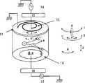
图4中示出了腐蚀室的简化结构图。天线线圈12设置在室上部中的石英基片11上,线圈12通过匹配盒13与RF功率源14连接。另外,RF功率源17通过匹配盒16与设置于相对侧上的基片下电极15连接。A simplified block diagram of the etch chamber is shown in FIG. 4 . The
如果RF电流加于基片上的天线线圈12上,则RF电流J在θ方向流动,在Z方向产生磁场B。If an RF current is applied to the
μoJ=rot Bμo J=rot B
根据电磁感应的法拉第定律,在θ方向产生感应电场E。
电子在感应电场E中在θ方向被加速,并与气体分子碰撞,产生等离子体。感应电场的方向是θ方向,因此,由于带电粒子与腐蚀室壁和基片碰撞造成的电荷消失的几率降低。因此甚至在1Pa的低压下,也可以产生高密度等离子体。另外,下游几乎没有磁场B,所以等离子体变为以片形散布的高密度等离子体。Electrons are accelerated in the θ direction in the induced electric field E, and collide with gas molecules to generate plasma. The direction of the induced electric field is the θ direction, therefore, the probability of charge disappearance due to the collision of the charged particles with the etching chamber wall and the substrate is reduced. Therefore, high-density plasma can be generated even at a low pressure of 1 Pa. In addition, there is almost no magnetic field B downstream, so the plasma becomes high-density plasma scattered in a sheet shape.
通过调节加于天线线圈12(加ICP功率)和基片下电极15(加偏置功率)上的RF功率源,可以分别控制等离子体密度和自偏压。另外,可以根据要处理的工件材料改变所加RF功率的频率。By adjusting the RF power source applied to the antenna coil 12 (with ICP power) and the substrate lower electrode 15 (with bias power), the plasma density and self-bias can be controlled respectively. Additionally, the frequency of the applied RF power can be varied depending on the workpiece material being processed.
为了用ICP腐蚀装置得到高密度等离子体,需要RF电流J在天线线圈12中以低损耗流动,并且,为了制造大表面积,天线线圈12的电感必须减小。因此开发出了具有多个螺旋线圈22的ICP腐蚀装置,其中天线线圈是隔开的,如图5所示。图5中,参考数字21表示石英基片,参考数字23和26表示匹配盒,24和27表示RF功率源。另外,支撑基片28的下电极25通过室下部的绝缘体29形成。如果使用其中采用了多个螺旋线圈的利用ICP的腐蚀装置,则可以对上述抗传导电材料进行很好地腐蚀。In order to obtain a high-density plasma with an ICP etching device, it is necessary for the RF current J to flow with low loss in the
本发明的申请人改变腐蚀条件,利用多螺旋ICP腐蚀装置(松下电器型号:E645),进行了许多试验。The applicant of the present invention changed the etching conditions, and conducted many experiments using a multi-screw ICP etching apparatus (Panasonic Model: E645).
首先,介绍用于各试验的腐蚀试验片。在绝缘基片(康宁#1737玻璃基片)上由氮氧化硅膜形成底膜(200nm厚),然后,通过溅射在其上形成金属层叠膜。使用纯度等于或高于6N的钨靶。另外,可以使用例如氩(Ar)、氪(Kr)或氙(Xe)中的一种气体或这些气体的混合气体。注意,操作者可以适当地控制例如溅射功率、气体压力和基片温度等膜淀积条件。First, corrosion test pieces used in each test will be described. A base film (200 nm thick) was formed from a silicon oxynitride film on an insulating substrate (Corning #1737 glass substrate), and then, a metal lamination film was formed thereon by sputtering. Use a tungsten target with a purity equal to or higher than 6N. In addition, one gas such as argon (Ar), krypton (Kr), or xenon (Xe) or a mixed gas of these gases may be used. Note that the operator can appropriately control film deposition conditions such as sputtering power, gas pressure, and substrate temperature.
金属层叠膜用由WNx(其中0<x<1)表示的氮化钨膜(厚30nm)作下层,用钨膜(370nm)作上层。The metal laminated film uses a tungsten nitride film (
这样得到的金属层叠膜几乎不含杂质元素,具体说,可以使得所含氧的量等于或小于30ppm。可以使电阻率等于或小于20μΩ.cm,一般为6-15μΩ.cm。另外,可以使膜应力从-5×10⁹达因/cm2到5×109达因/cm2。The metal laminated film thus obtained hardly contains impurity elements, specifically, it can be made to contain oxygen in an amount equal to or less than 30 ppm. Can make the resistivity equal to or less than 20μΩ. cm, generally 6-15μΩ. cm. In addition, the film stress can be made from -5×10⁹ dyne/cm2 to 5×10⁹ dyne/cm2 .
注意,整个说明书中,氮氧化硅膜是由SiOxNY表示的绝缘膜,表示绝缘膜含有预定比例的硅、氧和氮。Note that throughout the specification, the silicon oxynitride film is an insulating film represented by SiOxNY, indicating that the insulating film contains silicon, oxygen, and nitrogen in predetermined proportions.
利用多螺旋线圈ICP腐蚀装置,对腐蚀试验片进行金属层叠膜的构图实验。注意,在进行干法腐蚀时,无需说,要使用抗蚀剂,并将之构图成预定形状,形成抗蚀掩模图形(膜厚:1.5微米)。Using a multi-helical coil ICP corrosion device, the patterning experiment of the metal laminated film was carried out on the corrosion test piece. Note that, when performing dry etching, needless to say, a resist is used and patterned into a predetermined shape to form a resist mask pattern (film thickness: 1.5 µm).
图6A示出了腐蚀加工前腐蚀试验片模型的剖面图。图6A中,参考数字601表示基片,参考数字602表示底膜,603a和603b表示金属层叠膜(膜厚X=400nm),604a和604b表示抗蚀掩模图形(膜厚Y=1.5微米)。另外,图6B是展示腐蚀加工后状态的示图。Fig. 6A shows a cross-sectional view of a corrosion test piece model before corrosion processing. In Fig. 6A,
注意,如图6B所示,整个说明书中,锥角表示布线603的截面形状的锥形部分(倾斜部分)与底膜602间的夹角α。另外,该锥角可以表示为tanα=X/Z,其中Z为锥形部分的宽度,X为膜厚。Note that, as shown in FIG. 6B , throughout the specification, the taper angle represents the angle α between the tapered portion (inclined portion) of the cross-sectional shape of the wiring 603 and the
本发明的申请人改变该干法腐蚀的数个条件,观察了布线的截面形状。The applicant of the present invention changed several conditions of this dry etching, and observed the cross-sectional shape of wiring.
(实验1)(Experiment 1)
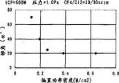
图1是展示锥角α与偏置功率间关系的示图。在20W、30W、40W、60W和100W,用13.56MHz,即,用0.128、0.192、0.256、0.384和0.64(W/cm2)的偏置功率密度,进行实验。注意,下电极为12.5cm×12.5cm。另外,抗蚀剂膜厚为1.5微米,气压为1.0Pa,气体组分为CF4/Cl2=30/30sccm(注意,sccm表示标准条件下的体积流速(cm3/分钟))。此外,ICP功率为500W,即,ICP功率密度为1.02 W/cm2。注意,整个说明书中,ICP功率除以lCP面积(直径为25cm)的值取作ICP功率密度(W/cm2)。FIG. 1 is a graph showing the relationship between cone angle α and bias power. At 20W, 30W, 40W, 60W, and 100W, with 13.56MHz, that is, with bias power densities of 0.128, 0.192, 0.256, 0.384, and 0.64 (W/cm2 ), conduct experiment. Note that the lower electrode is 12.5 cm x 12.5 cm. In addition, the resist film thickness is 1.5 μm, the gas pressure is 1.0 Pa, and the gas composition is CF4 /Cl2 =30/30 sccm (note that sccm represents the volume flow rate (cm3 /min) under standard conditions) . In addition, the ICP power is 500 W, that is, the ICP power density is 1.02 W/cm2 . Note that throughout the specification, the value of dividing the ICP power by the ICP area (25 cm in diameter) was taken as the ICP power density (W/cm2 ).
从图1可以理解,偏置功率密度越大,锥角α越小。另外,简单地调节偏置功率密度,可以形成希望的锥角α=5度-85度(较好是20-70度)。It can be understood from Figure 1 that the greater the bias power density, the smaller the cone angle α. In addition, simply adjusting the bias power density can form a desired cone angle α=5°-85° (preferably 20-70°).
注意,图7A示出了偏置功率设为20W(偏置功率密度:0.128W/cm2)时的截面SEM照片;图7B示出了偏置功率设为30W(偏置功率密度:0.192 W/cm2)时的截面SEM照片;图7C示出了偏置功率设为40W(偏置功率密度:0.256 W/cm2)时的截面SEM照片;图8A示出了偏置功率设为60W(偏置功率密度:0.384 W/cm2)时的截面SEM照片;图8B示出了偏置功率设为100W(偏置功率密度:0.64W/cm2)时的截面SEM照片。从图7A-8B的每幅照片可以观察到,锥角α形成在20-70度的范围内,通过改变偏置功率密度,可以控制锥角α。Note that Figure 7A shows the cross-sectional SEM photo when the bias power is set to 20W (bias power density: 0.128W/cm2 ); Figure 7B shows that the bias power is set to 30W (bias power density: 0 .192 W/cm2 ); Fig. 7C shows the cross-sectional SEM photo when the bias power is set to 40W (bias power density: 0.256 W/cm2 ); Fig. 8A shows the The cross-sectional SEM photo when the bias power is set to 60W (bias power density: 0.384 W/cm2 ); Fig. 8B shows that when the bias power is set to 100W (bias power density: 0.64W/cm2 ) SEM photographs of the cross-section. It can be observed from each of the photographs in FIGS. 7A-8B that the cone angle α is formed in the range of 20-70 degrees, and the cone angle α can be controlled by changing the bias power density.
可以认为这是由于钨和抗蚀剂间的选择性变小和抗蚀剂的再处理现象发生所造成的。This is considered to be due to the decrease in the selectivity between tungsten and the resist and the occurrence of a reprocessing phenomenon of the resist.
(实验2)(Experiment 2)
图2示出了锥角α与CF4的特定流速间的关系。用CF4/Cl2=20/40sccm、30/30sccm和40/20sccm的气体组分进行实验。气体压力为1.0Pa,偏置功率密度为0.128 W/cm2,抗蚀剂膜厚度为1.5微米,ICP功率为500W(ICP功率密度为1.02 W/cm2)。FIG. 2 shows the relationship between the cone angle α and the specific flow rate of CF4 . Experiments were carried out with gas compositions of CF4 /Cl2 =20/40 sccm, 30/30 sccm and 40/20 sccm. The gas pressure was 1.0 Pa, the bias power density was 0.128 W/cm2 , the resist film thickness was 1.5 μm, and the ICP power was 500 W (ICP power density was 1.02 W/cm2 ).
从图2可以知道,CF4的特定流速越大,钨和抗蚀剂间的选择性越大,布线的锥角α越大。另外,底膜的粗糙度变小。关于底膜的粗糙度,认为是由于CF4流速的增大(Cl2的流速减小)造成腐蚀的弱各向异性的缘故。另外,通过简单地调节CF4的特定流速,可以形成为5-85度(较好是60-80度)的希望锥角α。It can be known from Figure 2 that the greater the specific flow rate of CF4 , the greater the selectivity between tungsten and resist, and the greater the taper angle α of wiring. In addition, the roughness of the base film becomes smaller. Regarding the roughness of the bottom film, it is considered that the weak anisotropy of the corrosion is caused by the increase of the flow rate of CF4 (the decrease of the flow rate of Cl2 ). In addition, by simply adjusting the specific flow rate of CF4 , a desired cone angle α of 5-85 degrees (preferably 60-80 degrees) can be formed.
(实验3)(Experiment 3)
通过设定频率为13.56MHz、ICP功率为400W、500W和600W,即设定ICP的功率密度为0.82、1.02和1.22,进行实验。偏置功率为20W(偏置功率密度:0.128 W/cm2),抗蚀剂膜厚度1.5微米,气压为1.0Pa,气体组分为CF4/Cl2=30/30sccm。By setting the frequency as 13.56MHz and the ICP power as 400W, 500W and 600W, that is, setting the power density of ICP as 0.82, 1.02 and 1.22, the experiment is carried out. The bias power was 20 W (bias power density: 0.128 W/cm2 ), the resist film thickness was 1.5 µm, the gas pressure was 1.0 Pa, and the gas composition was CF4 /Cl2 =30/30 sccm.
在ICP功率密度变大时,钨的腐蚀速率变得较大,但腐蚀速率分布变为最差。另外,没发现锥角的特殊变化。When the ICP power density becomes larger, the corrosion rate of tungsten becomes larger, but the corrosion rate distribution becomes the worst. In addition, no particular change in the cone angle was found.
(实验4)(Experiment 4)
以1.0Pa和2.0Pa的气体压力进行实验。ICP功率为500W(ICP功率密度:1.02 W/cm2),气体组分CF4/Cl2=30/30sccm,偏置功率为20W(偏置功率密度:0.128 W/cm2),抗蚀剂膜厚1.5微米。Experiments were carried out at gas pressures of 1.0 Pa and 2.0 Pa. ICP power is 500W (ICP power density: 1.02 W/cm2 ), gas composition CF4 /Cl2 =30/30sccm, bias power is 20W (bias power density: 0.128 W/cm2 ) , The resist film thickness is 1.5 microns.
随着真空度变高,钨腐蚀速率变快,各向异性变强。另外,在2.0Pa时,锥形变为倒锥形。As the vacuum becomes higher, the corrosion rate of tungsten becomes faster and the anisotropy becomes stronger. In addition, at 2.0Pa, the taper becomes an inverted taper.
(实验5)(Experiment 5)
将腐蚀气体的总流速设定为60sccm和120sccm,进行实验。气体压力为1.0Pa,ICP功率为500W(ICP功率密度:1.02 W/cm2),气体组分CF4/Cl2=30/30sccm,偏置功率为20W(偏置功率密度:0.128W/cm2),抗蚀剂膜厚1.5微米。The experiment was performed with the total flow rate of the etching gas set at 60 sccm and 120 sccm. The gas pressure is 1.0Pa, the ICP power is 500W (ICP power density: 1.02 W/cm2 ), the gas composition CF4 /Cl2 =30/30sccm, and the bias power is 20W (bias power density: 0 .128W/cm2 ), the resist film thickness was 1.5 microns.
在腐蚀气体总流速较大的情况下,腐蚀速率变大一点。In the case where the total flow rate of the corrosive gas is larger, the corrosion rate becomes a little larger.
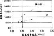
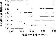
从上述实验的结果可知,锥角与钨和抗蚀剂间的选择性有关系,因为锥角主要受偏置功率密度条件的影响。图3示出了锥角与钨和抗蚀剂间选择性的关系。From the results of the above experiments, it can be seen that the taper angle is related to the selectivity between tungsten and resist, because the taper angle is mainly affected by the bias power density conditions. Figure 3 shows the taper angle as a function of selectivity between tungsten and resist.
偏置功率密度的改变对钨和抗蚀剂间选择性的影响大于对钨腐蚀速率的影响,并且,如果偏置功率密度变大,则存在钨与抗蚀剂间选择性下降的趋势。图9A示出了钨和抗蚀剂的腐蚀速率与偏置功率密度间的关系,而图9B示出了钨和抗蚀剂间选择性与偏置功率密度间的关系。The influence of the change of the bias power density on the selectivity between tungsten and resist is greater than that on the etching rate of tungsten, and if the bias power density becomes larger, there is a tendency for the selectivity between tungsten and resist to decrease. FIG. 9A shows the etch rate of tungsten and resist versus bias power density, and FIG. 9B shows the selectivity between tungsten and resist versus bias power density.
即,如图6A和6B所示,在腐蚀钨时,同时腐蚀抗蚀剂,因此,如果钨和抗蚀剂间的选择性大,则锥角变大,如果钨和抗蚀剂间的选择性小,则锥角变小。That is, as shown in FIGS. 6A and 6B, when tungsten is etched, the resist is etched simultaneously. Therefore, if the selectivity between tungsten and the resist is large, the taper angle becomes large. If the selectivity between tungsten and the resist The smaller the property, the smaller the cone angle.
另外,如果以相同方式使CF4的特定流速较小,则存在钨和抗蚀剂间选择性下降的趋势。图10A示出了钨和抗蚀剂的腐蚀速率与特定CF4气体流速间的关系,图10B示出了钨和抗蚀剂间选择性与特定CF4流速间的关系。Also, if the specific flow rate of CF4 is made smaller in the same manner, there is a tendency for the selectivity between tungsten and resist to decrease. Figure 10A shows the etch rate of tungsten and resist as a function of a specificCF4 gas flow rate, and Figure 10B shows the selectivity between tungsten and resist as a function of a specificCF4 flow rate.
另外,图11A示出了钨和抗蚀剂与ICP功率密度间的关系,图11B示出了钨和抗蚀剂间选择性与ICP功率密度间的关系。In addition, FIG. 11A shows the relationship between tungsten and resist and ICP power density, and FIG. 11B shows the relationship between the selectivity between tungsten and resist and ICP power density.
用由氮氧化硅膜构成的底膜(200nm厚)形成于绝缘基片上、且金属层叠膜(氮化钨膜和钨膜)形成于底膜上的试验片作在上述每个实验中腐蚀的试验片,但利用本发明,也可以利用选自钨膜、具有钨化合物作其主要成分的金属化合物膜薄膜、具有钨合金作其主要成分的金属合金膜中的一种薄膜或各薄膜层叠的层叠结构。然而,注意,不能应用与底膜的选择性等于或小于2.5的膜,和腐蚀速率极小的情况。例如,W-Mo合金膜(按重量计,W∶Mo=52∶48)与底膜(SiOxNY)的选择性等于或小于约1.5,腐蚀速率较小,为约50nm/分钟,因此,从可加工的观点来看,是不合适的。A test piece in which a base film (200 nm thick) composed of a silicon oxynitride film was formed on an insulating substrate, and a metal lamination film (tungsten nitride film and tungsten film) was formed on the base film was used for etching in each of the above experiments. However, using the present invention, it is also possible to use a thin film selected from a tungsten film, a metal compound film film having a tungsten compound as its main component, a metal alloy film having a tungsten alloy as its main component, or a laminated film. Layered structure. Note, however, that a film with a selectivity to the base film equal to or less than 2.5, and a case where the etch rate is extremely small, cannot be applied. For example, the selectivity between the W-Mo alloy film (by weight, W:Mo=52:48) and the bottom film (SiOxNY) is equal to or less than about 1.5, and the corrosion rate is small, about 50nm/min. Therefore, From the point of view of machinability, it is not suitable.
这里示出了钨膜作为一个实例,但对于一般公知的耐热导电材料(例如Ta、Ti、Mo、Cr、Nb和Si)来说,在使用ICP腐蚀装置时,图形的边缘容易制造成锥形。例如,如果选择腐蚀速率为140-160nm/分钟且选择率为6-8的Ta膜,则与腐蚀速率为70-90nm/分钟且选择率为2-4的W膜相比,其具有优异的值。因此,从可加工性角度出发,Ta膜也是合适的,但Ta的电阻率为20-30μΩcm,比W膜的电阻率10-16μΩcm稍高,这成为一个问题。A tungsten film is shown here as an example, but for generally known heat-resistant conductive materials (such as Ta, Ti, Mo, Cr, Nb and Si), when using an ICP etching device, the edges of the graphics are easily made into cones. shape. For example, if a Ta film with an etch rate of 140-160 nm/min and a selectivity of 6-8 is selected, it has excellent value. Therefore, the Ta film is also suitable from the viewpoint of processability, but the resistivity of Ta is 20-30 μΩcm, which is slightly higher than that of the W film, which is 10-16 μΩcm, and this becomes a problem.
另外,用CF4和Cl2的气体混合物作上述干腐蚀的腐蚀气体,但不特别限于此,可以用选自C2F6和C4F8中的含氟反应气和选自Cl2、SiCl4和BCl3的含氯气体的混合气。In addition, a gas mixture of CF4 and Cl2 is used as the etching gas for the above-mentioned dry etching, but it is not particularly limited thereto. A fluorine-containing reaction gas selected from C2 F6 and C4 F8 and a gas selected from Cl2 , A mixture of chlorine-containing gases of SiCl4 and BCl3 .
此外,不特别限于本发明的腐蚀条件,对于例如使用ICP腐蚀装置(松下电器型号:E645),且使用四氟化碳气体(CF4)和氯气(Cl2)的情况来说,操作都可以在以下范围内适当地确定腐蚀条件。In addition, the corrosion conditions of the present invention are not particularly limited, and the operation is possible for the case where, for example, an ICP corrosion apparatus (Panasonic Electric Model: E645) is used, and carbon tetrafluoride gas (CF4 ) and chlorine gas (Cl2 ) are used The corrosion conditions are appropriately determined within the following ranges.
腐蚀气总流速:60-120sccmTotal flow rate of corrosive gas: 60-120sccm
特定腐蚀气体流速:CF4/Cl2=30/30sccm-50/10sccmSpecific corrosive gas flow rate: CF4 /Cl2 =30/30sccm-50/10sccm
气压:1.0Pa-2.0PaAir pressure: 1.0Pa-2.0Pa
(腐蚀气体气氛的压力)(pressure of corrosive gas atmosphere)
ICP功率密度:0.61 W/cm2-2.04 W/cm2(ICP功率:300W-ICP power density: 0.61 W/cm2 -2.04 W/cm2 (ICP power: 300W-
1000W),频率为13MHz-60Mhz1000W), the frequency is 13MHz-60Mhz
偏置功率密度:0.064 W/cm2-3.2 W/cm2(偏置功率:10W-Bias power density: 0.064 W/cm2 -3.2 W/cm2 (bias power: 10W-
500W),频率为100kHz-60MHz,较好为6MHz-29MHz500W), the frequency is 100kHz-60MHz, preferably 6MHz-29MHz
基片温度:0℃-80℃,较好是70℃±10℃Substrate temperature: 0°C-80°C, preferably 70°C±10°C
注意,整个说明书中,术语“电极”表示术语“布线”的一部分,并表示与其它布线电连接的位置,或互连半导体层的位置。因此,为方便起见,尽管适当地区分“布线”和“电极”的应用,但使用“电极”一般意义上说包括“布线”。Note that throughout the specification, the term "electrode" means a part of the term "wiring", and means a position to be electrically connected to other wiring, or a position to interconnect semiconductor layers. Therefore, for the sake of convenience, the use of "electrode" includes "wiring" in a general sense, although applications of "wiring" and "electrode" are properly distinguished.
下面利用以下展示的各实施例详细介绍具有上述结构的本发明。The present invention having the above-mentioned structure will be described in detail below using various embodiments shown below.
(实施例1)(Example 1)
利用图12和13介绍本发明的实施例1。这里介绍一种有源矩阵基片,该基片上具有同时制造的像素TFT和像素部分的存储电容器及形成于像素部分的外围的驱动电路TFT。
实施例1的结构具有形成于有绝缘表面的基片101上的TFT,如图12所示。较好是使用玻璃基片或石英基片作基片101。如果耐热性可以接受的话,也可以使用塑料基片。此外,如果制造反射型显示器件,则还可以用具有形成于每个表面的绝缘膜的硅基片、金属基片或不锈钢基片作基片。The structure of
其上形成有TFT的基片101的表面上具有由含硅绝缘膜(整个说明书中一般是指氧化硅膜、氮化硅膜或氮氧化硅膜)构成的底膜102。例如,形成厚10-200nm(较好为50-100nm)的氮氧化硅膜102a和厚50-200nm(较好为100-150nm)的氢化氮氧化硅膜102b的层叠膜,所说氮氧化硅膜是利用等离子体CVD,由SiH4、NH3和N2O制造的,所说氢化氮氧化硅膜是由SiH4、NH3和H2类似制造的。这里示出了底膜102的两层结构,但也可以形成单层绝缘膜或具有两层以上的层叠膜。A
另外,在底膜102上形成TFT的有源层。用通过结晶具有非晶结构的半导体膜得到的结晶半导体膜作有源层。可以用例如激光退火、热退火(固相生长方法)、快速热退火(RTA法)或根据日本专利申请公开平7-130652中公开的技术利用催化元素的结晶法作结晶方法。注意,非晶半导体膜和微晶半导体膜可作为具有非晶结构的半导体膜,也可以用例如非晶硅锗膜等具有非晶结构的化合物半导体膜。In addition, an active layer of a TFT is formed on the base film 102 . A crystalline semiconductor film obtained by crystallizing a semiconductor film having an amorphous structure is used as the active layer. As the crystallization method, for example, laser annealing, thermal annealing (solid phase growth method), rapid thermal annealing (RTA method) or crystallization using catalytic elements according to the technique disclosed in Japanese Patent Application Laid-Open No. Hei 7-130652 can be used. Note that an amorphous semiconductor film and a microcrystalline semiconductor film may be used as a semiconductor film having an amorphous structure, and a compound semiconductor film having an amorphous structure such as an amorphous silicon germanium film may also be used.
利用等离子体CVD或溅射,由含硅的绝缘膜,形成厚40-150nm覆盖上述TFT有源层的栅绝缘膜130。在实施例1中形成厚120nm的氮氧化硅膜。另外,通过在SiH4和N2O中掺入O2制造的氮氧化硅膜内具有减小的固定电荷密度,因此,可作为实际应用的材料。自然,栅绝缘膜不限于这类氮氧化硅膜,可以用单层或层叠结构的其它含硅绝缘膜。The
形成于栅绝缘膜上的栅电极118-122和电容电极123采用具有层叠结构的耐热导电材料,所说层叠结构由导电金属氮化物膜形成的导电层(A)和由金属膜形成的导电层(B)构成。导电层(B)由选自Ta、Ti和W中的元素、或上述元素作其主要成分的合金、或上述元素组合的合金膜形成。在实施例1中,构图形成为导电层(A)、50nm厚的WN膜和形成为导电层(B)、250nm厚的W膜构成的导电层叠膜,完成栅电极118-122和电容器电极123。其中导电层(B)是通过利用纯度为6N的W靶、并引入Ar气和氮(N2)气的溅射形成的。注意,进行腐蚀,在栅电极118-123的边缘形成锥形部分。该腐蚀工艺利用ICP腐蚀装置进行。该技术的细节如本发明的实施模式中所介绍的。实施例1中,利用CF4和Cl2的气体混合物作腐蚀气、用每种气体30sccm的流速、设定为3.2 W/cm2(频率:13.56MHz)的ICP功率密度、设定为0.224 W/cm2(频率:13.56MHz)的偏置功率密度、和1.0Pa的气体压力进行腐蚀。利用这些腐蚀条件,在栅极118-122和电容电极123的边缘部分形成锥形部分,其中厚度从边缘部分向着内部逐渐增大。该角度可以制成为25-35度,较好是30度。The gate electrodes 118-122 and
注意,为了在形成具有锥形的栅电极118-122和电容电极123时进行腐蚀而不留下任何残留物,进行重叠腐蚀,其中腐蚀时间增加10-20%,因此,栅绝缘膜130具有实际变薄的部分。Note that in order to perform etching without leaving any residue when forming the gate electrodes 118-122 and
另外,在实施例1中,为形成LDD区,用在其边缘具有锥形部分的栅电极118-122作掩模,通过离子掺杂,以自对准方式,在有源层中掺入产生n型或p型导电的杂质元素。另外,为形成合适且希望的LDD区,用抗蚀剂图形作掩模,通过离子掺杂,在有源层内掺入产生n型或p型导电的杂质元素。In addition, in
于是在驱动电路的第一p沟道TFT(A)200a中,形成有源层内的沟道形成区206、与栅极重叠的LDD区207、由高浓度p型杂质区构成的源区208、和漏区209。第一n沟道TFT(A)201a在有源层内具有沟道形成区210、由低浓度n杂质区构成且与栅极119重叠的LDD区211、由高浓度n型杂质区构成的源区212和漏区213。与栅极119重叠的LDD区表示为Lov,对于沟道长度为3-7微米的沟道来说,在沟道的纵向,其长度为0.1-1.5微米,较好是0.3-0.8微米。Lov的长度控制栅电极119的厚度和锥形部分的角度。Then, in the first p-channel TFT (A) 200a of the driver circuit, a
另外,类似地,驱动电路的第二p沟道TFT(A)202a的有源层具有沟道形成区214、与栅极120重叠的LDD区215、由高浓度p型杂质区形成的源区216和漏区217。在第二n沟道TFT(A)203a中,有源层具有沟道形成区218、与栅电极121重叠的LDD区219、由高浓度n型杂质区形成的源区220和漏区221。LDD区219具有与LDD区211相同的结构。像素TFT204在有源层内具有沟道形成区222a和222b、由低浓度n型杂质区形成的LDD区223a和223b、由高浓度n杂质区形成的源或漏区225-227。LDD区223 a和223b具有与LDD区211相同的结构。此外,存储电容205由电容布线123、栅绝缘膜和与像素TFT204的漏区227连接的半导体层228和229形成。图12中,驱动电路的n沟道TFT和p沟道TFT具有单栅结构,其中一个栅极提供在源和漏对之间,像素TFT具有双栅结构,但所有TFT都可以给予单栅结构,在源和漏对之间提供多个栅极的多栅结构也不会造成问题。In addition, similarly, the active layer of the second p-channel TFT (A) 202a of the driver circuit has a
另外,有覆盖栅电极的保护绝缘膜142和绝缘膜130。保护绝缘膜可由氧化硅膜、氮氧化硅膜、氮化硅膜或这些膜组合的层叠膜构成。In addition, there are protective
此外,还有由有机绝缘材料构成的、覆盖保护绝缘膜142的层间绝缘膜143。可用例如聚酰亚胺、丙烯酸、聚酰胺、聚酰亚胺酰胺和BCB(苯并环丁烯)作有机树脂材料。In addition, there is an interlayer insulating
另外,层间绝缘膜143上具有源布线和漏布线,用于通过接触孔连接形成于各有源层上的源区和漏区。注意,源布线和漏布线具有层叠结构,该层叠结构由参考数字144a-154a表示的Ti和铝的层叠膜和参考数字144b-154b表示的透明导电膜构成。另外,漏布线153a和153b还用作像素电极,透明导电膜的合适材料有氧化铟和氧化锌合金(In2O3-ZnO)和氧化锌(ZnO),为了另外增大透射率和导电性,可以使用例如加入了镓(Ga)的氧化锌(ZnO∶Ga)等材料。In addition, there are source wiring and drain wiring on the
利用上述结构,构成每种电路的TFT的结构可以根据像素TFT和驱动电路要求的规格优化,可以加强半导体器件的工作性能和可靠性。此外,通过用具有耐热性的导电材料形成栅电极,LDD区和源区和漏区的激活变得较容易。With the above structure, the structure of the TFT constituting each circuit can be optimized according to the specifications required by the pixel TFT and the driving circuit, and the working performance and reliability of the semiconductor device can be enhanced. In addition, by forming the gate electrode with a heat-resistant conductive material, the activation of the LDD region and the source and drain regions becomes easier.
此外,在形成通过栅绝缘膜与栅极重叠的LDD区期间,通过形成具有为控制导电类型掺入的杂质元素浓度梯度的LDD区,预计可以增强特别是漏区附近的电场驰豫效应。Furthermore, during the formation of the LDD region overlapping the gate through the gate insulating film, by forming the LDD region with a concentration gradient of an impurity element doped for conductivity type control, it is expected that the electric field relaxation effect especially near the drain region can be enhanced.
在作为透射型液晶显示器件时,可应用图12所示的有源矩阵基片。As a transmissive liquid crystal display device, the active matrix substrate shown in Fig. 12 can be used.
下面利用图13介绍应用图12所示有源矩阵基片的有源矩阵型液晶显示器件。Next, an active matrix type liquid crystal display device using the active matrix substrate shown in FIG. 12 will be described using FIG. 13. FIG.
首先,构图有源矩阵基片上的树脂膜,形成棒状间隔件405a-405e和406。间隔件的位置可任意设定。注意,可以利用通过分散尺寸为几微米的晶粒形成间隔件的方法。First, the resin film on the active matrix substrate is patterned to form rod-shaped spacers 405a-405e and 406. The position of the spacer can be set arbitrarily. Note that a method of forming spacers by dispersing crystal grains having a size of several micrometers may be utilized.
然后,在有源矩阵基片的像素部分中,由例如聚酰亚胺树脂等材料形成校准膜407,以使液晶取向。形成校准膜后,进行研磨处理,使液晶分子取向,以便具有某一固定的预定倾角。Then, in the pixel portion of the active matrix substrate, an
在相对侧的相对基片401上形成光屏蔽膜402、透明导电膜403、和校准膜404。光屏蔽膜402由例如Ti膜、Cr膜或Al膜形成,厚为150-300nm。然后,利用密封部件408将其上形成有像素部分和驱动电路的有源矩阵基片和相对基片接合在一起。On the opposing
然后,在两基片间注入液晶材料409。液晶材料可使用已知的液晶材料。例如,除TN液晶外,也可以使用指示透射率随电场连续变化的电-光响应的无阈值反铁电混合液晶。某些无阈值反铁电混合液晶具有V形电-光响应特性。于是完成了图13所示的反射型有源矩阵液晶显示器件。Then, a
(实施例2)(Example 2)
利用图14,实施例2示出了一个制造使用不同于上述实施例1(顶栅TFT)的底栅TFT的显示器件的实例。Using FIG. 14, Embodiment 2 shows an example of manufacturing a display device using a bottom-gate TFT different from the above-described Embodiment 1 (top-gate TFT).
首先,在绝缘基片1801上溅射形成金属层叠膜。金属层叠膜用氮化钨膜作底层,用W膜作顶层。注意,与基片接触的底膜也可由例如表示为SiOxNy的氮氧化硅膜形成。然后,通过光刻形成用于得到希望栅布线图形的抗蚀掩模。First, a metal lamination film is formed on an insulating substrate 1801 by sputtering. The metal lamination film uses a tungsten nitride film as the bottom layer and a W film as the top layer. Note that the base film in contact with the substrate may also be formed of, for example, a silicon oxynitride film expressed as SiOxNy. Then, a resist mask for obtaining a desired gate wiring pattern is formed by photolithography.
需要例如栅绝缘膜和沟道形成区等结构形成于底栅TFT的栅布线上。为了增强底栅结构TFT的特性、在栅布线上形成覆盖膜和栅绝缘膜的耐压,栅布线1802-1805的锥角较好是等于或小于60度,更好是等于或小于40度。Structures such as a gate insulating film and a channel formation region need to be formed on the gate wiring of the bottom gate TFT. In order to enhance the characteristics of TFT with bottom gate structure and form the covering film and gate insulating film on the gate wiring to withstand voltage, the taper angle of the gate wiring 1802-1805 is preferably equal to or less than 60 degrees, more preferably equal to or less than 40 degrees.
然后,如本发明的实施模式中介绍的,利用ICP腐蚀装置,并选择合适的偏置功率和特定气体流速,使栅布线1802-1805的锥角等于或小于60度,更好是等于或小于40度。随后的处理可使用已知技术,这里不再具体介绍。Then, as introduced in the embodiment mode of the present invention, utilize ICP etching device, and select suitable bias power and specific gas flow rate, make the taper angle of gate wiring 1802-1805 be equal to or less than 60 degrees, more preferably be equal to or less than 40 degree. Subsequent processing can use known techniques, which will not be described in detail here.
图14中,参考数字1814表示CMOS电路,参考数字1815表示n沟道TFT,1816表示像素TFT,1817表示层间绝缘膜,1818a表示像素电极,1818b表示ITO膜。形成ITO膜1818b的目的是通过粘合剂1822与例如FPC 1823等外部端子连接。另外,参考数字1819表示液晶材料,1820表示相对电极。此外,参考数字1801表示第一基片,1808表示密封区,1807和1809-1812表示棒形间隔件,1821表示第二基片。In FIG. 14, reference numeral 1814 denotes a CMOS circuit, reference numeral 1815 denotes an n-channel TFT, 1816 denotes a pixel TFT, 1817 denotes an interlayer insulating film, 1818a denotes a pixel electrode, and 1818b denotes an ITO film. The purpose of forming the ITO film 1818b is to connect with an external terminal such as an FPC 1823 through an adhesive 1822. In addition, reference numeral 1819 denotes a liquid crystal material, and 1820 denotes an opposite electrode. In addition, reference numeral 1801 denotes a first substrate, 1808 denotes a sealing region, 1807 and 1809-1812 denote bar-shaped spacers, and 1821 denotes a second substrate.
注意,可以自由组合实施例2和实施例1。Note that Embodiment 2 and
(实施例3)(Example 3)
图15A-15F展示了利用本发明在绝缘表面上形成各种布线结构的例子。图15A示出了由钨作其主要成分的材料1501构成、且形成于具有绝缘表面的膜(或基片)1500上的单层结构布线的剖面图。该布线通过构图由采用纯度为6N(99.9999%)的靶、用一种气体如氩(Ar)气作溅射气体的溅射形成的膜形成。注意,通过将基片温度设为等于或低于300℃,并将溅射气体压力设为等于或高于1.0Pa,来控制应力,其它条件(例如溅射功率)可由操作者适当地确定。15A-15F show examples of forming various wiring structures on insulating surfaces using the present invention. FIG. 15A shows a cross-sectional view of a single-layer structure wiring composed of a material 1501 composed of tungsten as its main component and formed on a film (or substrate) 1500 having an insulating surface. The wiring is formed by patterning a film formed by sputtering using a target having a purity of 6N (99.9999%), using a gas such as argon (Ar) gas as a sputtering gas. Note that the stress is controlled by setting the substrate temperature to be equal to or lower than 300°C and the sputtering gas pressure to be equal to or higher than 1.0Pa, and other conditions such as sputtering power can be appropriately determined by the operator .
在进行上述构图时,根据例如偏置功率密度,利用本发明实施模式中所介绍的方法控制锥角α。In performing the above-mentioned patterning, the taper angle α is controlled by the method described in the embodiment mode of the present invention according to, for example, the bias power density.
这样得到的布线1501的截面形状具有希望的锥角α。另外,布线1501中几乎没有杂质元素,特别是可使所含氧量等于或小于30ppm,使电阻率等于或小于20μΩcm,一般为6-15μΩcm。另外,可以将膜应力控制在-5×10¹⁰-5×10¹⁰达因/cm2。The cross-sectional shape of wiring 1501 thus obtained has a desired taper angle α. In addition, there is almost no impurity element in the wiring 1501, especially the oxygen content can be made equal to or less than 30ppm, and the resistivity can be equal to or less than 20μΩcm, generally 6-15μΩcm. In addition, the film stress can be controlled at -5×10¹⁰ -5×10¹⁰ dynes/cm2 .
图15B示出了与实施例1的栅极类似的两层结构。注意,氮化钨(WNx)用作下层,钨用作上层。另外,注意,氮化钨膜1502的厚度可以设为从10-50nm(较好是10-30nm),钨膜1503的厚度可以设为200-400nm(较好是250-350nm)。实施例3中,利用溅射,在不暴露于大气的情况下,连续层叠两层膜。FIG. 15B shows a two-layer structure similar to the gate electrode of
图15C是利用绝缘膜1505覆盖由具有钨作其主要成分的材料构成、且形成于具有绝缘表面的膜(或基片)1500上的布线1504的例子。绝缘膜1505由氮化硅膜、氧化硅膜和氮氧化硅膜SiOxNy(其中0<x,y<1)形成,或由这些膜组合的层叠膜形成。15C is an example of covering with an insulating film 1505 a wiring 1504 composed of a material having tungsten as its main component and formed on a film (or substrate) 1500 having an insulating surface. The insulating film 1505 is formed of a silicon nitride film, a silicon oxide film, and a silicon oxynitride film SiOxNy (where 0<x, y<1), or a laminated film of a combination of these films.
图15D是用氮化钨膜1507覆盖由具有钨作其主要成分的材料构成、且形成于具有绝缘表面的膜(或基片)1500上的布线1506的表面的例子。注意,如果对图15A所示状态的布线进行例如等离子体硝化等硝化处理,则可以得到图15D的结构。15D is an example of covering the surface of a wiring 1506 formed of a material having tungsten as its main component and formed on a film (or substrate) 1500 having an insulating surface with a tungsten nitride film 1507. Note that if the wiring in the state shown in FIG. 15A is subjected to nitrification treatment such as plasma nitrification, the structure of FIG. 15D can be obtained.
图15E是用氮化钨膜1510和1508覆盖由具有钨作其主要成分的材料构成、且形成于具有绝缘表面的膜(或基片)1500上的布线1509的例子。注意,如果对图15B所示状态的布线进行例如等离子体硝化等硝化处理,则可以得到图15E的结构。15E is an example of covering a wiring 1509 made of a material having tungsten as its main component and formed on a film (or substrate) 1500 having an insulating surface with tungsten nitride films 1510 and 1508. Note that if the wiring in the state shown in FIG. 15B is subjected to nitrification treatment such as plasma nitrification, the structure of FIG. 15E can be obtained.
图15F是形成图15E状态后利用绝缘膜1511覆盖的例子。绝缘膜1511可由氮化硅膜、氧化硅膜、氮氧化硅膜或这些膜的层叠膜形成。FIG. 15F is an example of covering with an insulating film 1511 after the state of FIG. 15E is formed. The insulating film 1511 can be formed of a silicon nitride film, a silicon oxide film, a silicon nitride oxide film, or a laminated film of these films.
所以,本发明可应用于各种布线结构。可以自由地组合实施例3的结构与实施例1和2所示结构。Therefore, the present invention is applicable to various wiring structures. The structure of Embodiment 3 and the structures shown in
(实施例4)(Example 4)
实施例4中介绍了一种将本发明应用于在硅基片上制造的反射型液晶显示器件的情况。代替实施例1中包括结晶硅膜的有源层,直接在硅基片(硅晶片)中掺入产生n型或p型导电的杂质元素,可以实现这种TFT结构,另外,该结构是反射型的,因此,可以用具有高反射率(例如,铝、银、或它们的合金(Al-Ag合金))的金属膜等作像素电极。In Embodiment 4, a case where the present invention is applied to a reflective liquid crystal display device fabricated on a silicon substrate is described. Instead of the active layer comprising a crystalline silicon film in
注意,可以自由地组合实施例4的结构与实施例1-3的结构。Note that the structure of Embodiment 4 and the structures of Embodiments 1-3 can be freely combined.
(实施例5)(Example 5)
当在常规MOSFET上形成层间绝缘膜,然后在其上形成TFT时,可以应用本发明。换言之,可以实现三维结构的半导体器件。另外,可以便用例如SIMOX、Smart-cut(SOITEC公司的一种商标)或ELTRAN(佳能公司的一种商标)等SOI基片。The present invention can be applied when an interlayer insulating film is formed on a conventional MOSFET and then a TFT is formed thereon. In other words, a three-dimensional structured semiconductor device can be realized. Alternatively, an SOI substrate such as SIMOX, Smart-cut (a trademark of SOITEC Corporation) or ELTRAN (a trademark of Canon Corporation) may be used.
注意,可以自由组合实施例5的结构与实施例1-4的结构。Note that the structure of Embodiment 5 can be freely combined with the structures of Embodiments 1-4.
(实施例6)(Example 6)
可以将本发明应用于有源矩阵EL显示器。图16示出了一个例子。The present invention can be applied to active matrix EL displays. Figure 16 shows an example.
图16是有源矩阵EL显示器的电路图。参考数字81表示像素部分,X方向驱动电路82和Y方向驱动电路83形成于其外围。另外,像素部分81中的每个像素包括开关TFT 84、电容器85、电流控制TFT86和有机EL元件87,开关TFT84接X方向信号线88a(或88b),和Y方向信号线89a(或89b,89c)。另外,电源线90a和90b接电流控制TFT86。Fig. 16 is a circuit diagram of an active matrix EL display. Reference numeral 81 denotes a pixel portion, and an X-direction driving circuit 82 and a Y-direction driving circuit 83 are formed on the periphery thereof. In addition, each pixel in the pixel portion 81 includes a switch TFT 84, a capacitor 85, a current control TFT 86, and an organic EL element 87, and the switch TFT 84 is connected to the X direction signal line 88a (or 88b), and the Y direction signal line 89a (or 89b, 89c). In addition, the current control TFT 86 is connected to the power supply lines 90a and 90b.
在本实施例中的有源矩阵EL显示器中,通过组合图12中的p沟道TFT200a或202a和图12中的n沟道TFT201a或203a,可以形成用于X方向驱动电路82、Y方向驱动电路83和电流控制TFT86的TFT。用于开关TFT84的TFT可由图12中的n沟道TFT204形成。In the active matrix EL display in this embodiment, by combining the p-
可以自由组合本发明的有源矩阵EL显示器与实施例1-5的结构。The active matrix EL display of the present invention can be freely combined with the structures of Examples 1-5.
(实施例7)(Example 7)
下面结合图17介绍实施例1中图13所示有源矩阵液晶显示器件的结构。有源矩阵基片(第一基片)包括形成于玻璃基片801上的像素部分802、栅侧驱动电路803和源侧驱动电路804。像素部分的像素TFT805(对应于图13中的像素TFT204)是n沟道TFT,并与像素电极806和存储电极807(对应于图13中的存储电容205)连接。The structure of the active matrix liquid crystal display device shown in FIG. 13 in
外围中的驱动电路由CMOS电路作为基础。栅侧驱动电路803和源侧驱动电路804分别通过栅布线808和源布线809连接像素部分802。另外,输入-输出布线(连接布线)812和813设于与用于将信号传输到驱动电路的FPC810连接的外部输入-输出端子811中。参考数字814是相对基片(第二基片)。The drive circuits in the periphery are based on CMOS circuits. The gate-
注意,尽管本说明书中图17所示的半导体器件是指有源矩阵液晶显示器件,但图17所示的用FPC完成的液晶屏板一般称作液晶组件。因此,可以称该实施例的有源矩阵液晶显示器件作液晶组件。Note that although the semiconductor device shown in FIG. 17 in this specification refers to an active matrix liquid crystal display device, the liquid crystal panel completed with FPC shown in FIG. 17 is generally called a liquid crystal module. Therefore, the active matrix liquid crystal display device of this embodiment can be called a liquid crystal module.
(实施例8)(Embodiment 8)
通过实施本发明制造的TFT可应用于各种电-光器件。即,本发明可应用于引入这种电-光器件作显示部分的所有电子设备。TFTs manufactured by implementing the present invention can be applied to various electro-optical devices. That is, the present invention is applicable to all electronic equipment incorporating such an electro-optical device as a display portion.
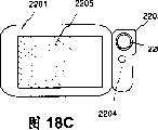
这些电子设备的例子包括:视频摄像机、数字摄像机、头戴式显示器(眼镜式显示器)、可穿式显示器、汽车导航系统、个人电脑和便携式信息终端(例如移动电脑,便携式电话,电子计事本等)。图18A-18F示出这些电子设备的例子。Examples of these electronic devices include: video cameras, digital cameras, head-mounted displays (glasses displays), wearable displays, car navigation systems, personal computers and portable information terminals (such as mobile computers, portable phones, electronic organizers, etc.) wait). Examples of these electronic devices are shown in Figures 18A-18F.
图18A示出了个人电脑,包括:主体2001、图像输入部分2002、显示部分2003、键盘2004。本发明可应用于图像输入部分2002、显示部分2003或其它信号驱动电路。FIG. 18A shows a personal computer including: a main body 2001 , an image input section 2002 , a display section 2003 , and a keyboard 2004 . The present invention can be applied to the image input section 2002, the display section 2003, or other signal drive circuits.
图18B示出了视频摄像机,包括:主体2101、显示部分2102、音频输入部分2103、操作开关2104、电池2105和图像接收部分2106。本发明可应用于显示部分2102、音频输入部分2103或其它信号控制电路。FIG. 18B shows a video camera including: a main body 2101 , a display portion 2102 , an audio input portion 2103 , an operation switch 2104 , a battery 2105 and an image receiving portion 2106 . The present invention can be applied to the display section 2102, the audio input section 2103, or other signal control circuits.
图18C示出了便携式电脑,包括:主体2201、摄像部分2202、图像接收部分2203、操作开关2204和显示部分2205。本发明可应用于显示部分2205或其它信号驱动电路。FIG. 18C shows a portable computer including: a
图18D示出了眼镜式显示器,包括:主体2301、显示部分2302、臂部2303。本发明可应用于显示部分2302或其它信号驱动电路。FIG. 18D shows a glasses-type display, including: a main body 2301 , a display portion 2302 , and an arm portion 2303 . The present invention can be applied to the display portion 2302 or other signal drive circuits.
图18E示出了采用存储有程序的记录媒质(此后称之为记录媒质)的播放器,包括:主体2401、显示部分2402、扬声器单元2403、记录媒质2404和操作开关2405。注意,使用DVD(数字通用盘)或CD作该装置的记录媒质,能够再现音乐程序,显示图像,并进行游戏,或用于国际互联网。本发明可应用于显示器件2402和其它信号驱动电路。18E shows a player using a recording medium (hereinafter referred to as a recording medium) storing a program, including: a main body 2401, a display portion 2402, a speaker unit 2403, a recording medium 2404, and operation switches 2405. Note that, using DVD (Digital Versatile Disc) or CD as a recording medium of the device, music programs can be reproduced, images can be displayed, and games can be played, or used for the Internet. The present invention can be applied to the display device 2402 and other signal driving circuits.
图18F示出了数字摄像机,包括:主体2501、显示部分2502、目镜部分2503、操作开关2504、和图像接收单元(图中未示出)。本发明可应用于显示单元2502或其它信号驱动电路。Fig. 18F shows a digital camera including: a main body 2501, a display portion 2502, an eyepiece portion 2503, an operation switch 2504, and an image receiving unit (not shown in the figure). The present invention can be applied to the display unit 2502 or other signal driving circuits.
如上所述,本发明的应用范围很宽,可应用于各种领域的电子设备。另外,本实施例的电子设备可利用实施例1-7的任何一种组合实现。As described above, the present invention has a wide application range and can be applied to electronic equipment in various fields. In addition, the electronic device of this embodiment can be realized by any combination of Embodiments 1-7.
(实施例9)(Example 9)
通过实施本发明制造的TFT可应用于各种电-光器件。即,本发明可应用于引入这种电-光器件作显示部分的电子设备。TFTs manufactured by implementing the present invention can be applied to various electro-optical devices. That is, the present invention can be applied to electronic equipment incorporating such an electro-optical device as a display portion.
关于这种电子设备,可以给出投影仪(背置型或前置型)等。图19A-19D示出了几个例子。As such electronic equipment, a projector (rear type or front type) and the like can be given. Several examples are shown in Figures 19A-19D.
图19A示出了前置型投影仪,它包括投影系统2601和屏2602。本发明可应用于构成投影系统2601的一部分的液晶显示器件2808或其它信号控制电路。FIG. 19A shows a front projector including a
图19B示出了背置型投影仪,它包括主体2701、投影系统2702、反射镜2703、屏2704。本发明可应于构成投影系统2702一部分的液晶显示器件2808或其它信号控制电路。FIG. 19B shows a rear projector, which includes a main body 2701 , a projection system 2702 , a mirror 2703 , and a screen 2704 . The present invention may be applied to liquid
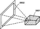
图19C是展示图19A和19B中的显示器件2601和2702的结构实例的示图。投影系统2601和2702包括:光源光学系统2801、反射镜2802和2804-2806、分光镜2803、棱镜2807、液晶显示器件2808、相差板2809、和投影光学系统2810构成。投影光学系统2810由包括透镜的光学系统构成。尽管本实施例示出了三板系统的例子,但并不限于这种系统,也可以采用单板系统光学系统。操作者可以在图19C中箭头所示的光学路径中适当地设置例如光学透镜、偏振膜、调相膜、IR膜等。Fig. 19C is a diagram showing a structural example of the
此外,图19D示出了图19C的光源光学系统2801的结构的实例。该例中,光源光学系统2801包括反射器2811、光源2812、透镜阵列2813和2814、偏振转换元件2815及会聚透镜2816。顺便提及,图19D所示的光源光学系统是一个实例,本发明不限于该图所示的结构。例如,操作者可以在该光源光学系统中适当地设置光学透镜、偏振膜、调相膜、IR膜等。Furthermore, FIG. 19D shows an example of the structure of the light source
如上所述,本发明的应用范围非常广泛,可应用于各种领域的电子设备。另外,本例的电子设备可利用实施例1-3和7的任何组合的结构实现。然而,如果本实施例的投影系统是透射型液晶显示器件,无需说它们不能应用于反射型液晶显示器件。As described above, the application range of the present invention is very wide, and can be applied to electronic devices in various fields. In addition, the electronic device of this example can be realized by using any combination of the structures of Embodiments 1-3 and 7. However, if the projection systems of this embodiment are transmissive liquid crystal display devices, it goes without saying that they cannot be applied to reflective liquid crystal display devices.
通过适当地设置通过能够控制布线的锥角α的偏置功率和特定气体流速等条件,可以提高相对于底膜的选择性,同时,根据本发明可以得到希望的锥角α。结果,形成于布线上的膜的覆盖较好,因此可以减少例如布线剥落、布线漏电和短路等缺陷。By appropriately setting conditions such as bias power and specific gas flow rate capable of controlling the taper angle α of the wiring, the selectivity to the base film can be improved, and at the same time, the desired taper angle α can be obtained according to the present invention. As a result, the coverage of the film formed on the wiring is better, so defects such as peeling of the wiring, wiring leakage, and short circuit can be reduced.
另外,可以腐蚀得使该部分内具有良好的分布,并可以得到均匀的布线形状。In addition, etching can be performed so as to have a good distribution in this portion, and a uniform wiring shape can be obtained.
另外,本发明可应用于接触孔等的开口工艺。In addition, the present invention can be applied to an opening process of a contact hole or the like.
Claims (31)
Applications Claiming Priority (2)
| Application Number | Priority Date | Filing Date | Title |
|---|---|---|---|
| JP206954/1999 | 1999-07-22 | ||
| JP11206954AJP2001035808A (en) | 1999-07-22 | 1999-07-22 | Wiring, method of manufacturing the same, semiconductor device provided with the wiring, and dry etching method |
Related Child Applications (3)
| Application Number | Title | Priority Date | Filing Date |
|---|---|---|---|
| CN200410056020.7ADivisionCN1567078B (en) | 1999-07-22 | 2000-07-24 | Wiring and manufacturing method thereof, semiconductor device including said wiring, and dry etching method |
| CNB2004100566082ADivisionCN1327284C (en) | 1999-07-22 | 2000-07-24 | display device |
| CN200610100376.5ADivisionCN1881537B (en) | 1999-07-22 | 2000-07-24 | Method for manufacturing active matrix display |
Publications (2)
| Publication Number | Publication Date |
|---|---|
| CN1282107Atrue CN1282107A (en) | 2001-01-31 |
| CN1185716C CN1185716C (en) | 2005-01-19 |
Family
ID=16531776
Family Applications (5)
| Application Number | Title | Priority Date | Filing Date |
|---|---|---|---|
| CN00121738.0AExpired - Fee RelatedCN1185716C (en) | 1999-07-22 | 2000-07-24 | Wiring and manufacturing method thereof, semiconductor device including said wiring, and dry etching method |
| CNB2004100566082AExpired - LifetimeCN1327284C (en) | 1999-07-22 | 2000-07-24 | display device |
| CN200610100376.5AExpired - Fee RelatedCN1881537B (en) | 1999-07-22 | 2000-07-24 | Method for manufacturing active matrix display |
| CN200410056020.7AExpired - Fee RelatedCN1567078B (en) | 1999-07-22 | 2000-07-24 | Wiring and manufacturing method thereof, semiconductor device including said wiring, and dry etching method |
| CN200610099986.8APendingCN1933142A (en) | 1999-07-22 | 2000-07-24 | Wiring and manufacturing method thereof, semiconductor device comprising said wiring, and dry etching method |
Family Applications After (4)
| Application Number | Title | Priority Date | Filing Date |
|---|---|---|---|
| CNB2004100566082AExpired - LifetimeCN1327284C (en) | 1999-07-22 | 2000-07-24 | display device |
| CN200610100376.5AExpired - Fee RelatedCN1881537B (en) | 1999-07-22 | 2000-07-24 | Method for manufacturing active matrix display |
| CN200410056020.7AExpired - Fee RelatedCN1567078B (en) | 1999-07-22 | 2000-07-24 | Wiring and manufacturing method thereof, semiconductor device including said wiring, and dry etching method |
| CN200610099986.8APendingCN1933142A (en) | 1999-07-22 | 2000-07-24 | Wiring and manufacturing method thereof, semiconductor device comprising said wiring, and dry etching method |
Country Status (6)
| Country | Link |
|---|---|
| US (3) | US7666718B2 (en) |
| EP (1) | EP1071124A3 (en) |
| JP (1) | JP2001035808A (en) |
| KR (4) | KR100727274B1 (en) |
| CN (5) | CN1185716C (en) |
| TW (2) | TW552643B (en) |
Cited By (7)
| Publication number | Priority date | Publication date | Assignee | Title |
|---|---|---|---|---|
| US7169710B2 (en) | 2001-03-27 | 2007-01-30 | Semiconductor Energy Laboratory Co., Ltd. | Wiring and method of manufacturing the same, and wiring board and method of manufacturing the same |
| US7649207B2 (en) | 2006-05-17 | 2010-01-19 | Au Optronics Corp. | Thin film transistor |
| US8247245B2 (en) | 2006-11-10 | 2012-08-21 | Au Optronics Corp. | Pixel structure and method for fabricating the same |
| CN102024696B (en)* | 2009-09-11 | 2012-08-22 | 中芯国际集成电路制造(上海)有限公司 | Opening and forming method thereof |
| CN103117219A (en)* | 2013-01-30 | 2013-05-22 | 常州同泰光电有限公司 | Morphology-controllable etching method |
| US8558823B2 (en) | 2006-11-16 | 2013-10-15 | Au Optronics Corp. | Liquid crystal display and gate modulation method thereof |
| CN109671622A (en)* | 2018-12-20 | 2019-04-23 | 深圳市华星光电半导体显示技术有限公司 | The preparation method of Cu film, thin film transistor (TFT) and array substrate |
Families Citing this family (38)
| Publication number | Priority date | Publication date | Assignee | Title |
|---|---|---|---|---|
| TW480554B (en)* | 1999-07-22 | 2002-03-21 | Semiconductor Energy Lab | Semiconductor device and manufacturing method thereof |
| JP2001035808A (en)* | 1999-07-22 | 2001-02-09 | Semiconductor Energy Lab Co Ltd | Wiring, method of manufacturing the same, semiconductor device provided with the wiring, and dry etching method |
| TWI224806B (en)* | 2000-05-12 | 2004-12-01 | Semiconductor Energy Lab | Semiconductor device and manufacturing method thereof |
| US6872604B2 (en)* | 2000-06-05 | 2005-03-29 | Semiconductor Energy Laboratory Co., Ltd. | Method of fabricating a light emitting device |
| US6809012B2 (en)* | 2001-01-18 | 2004-10-26 | Semiconductor Energy Laboratory Co., Ltd. | Method of making a thin film transistor using laser annealing |
| JP2002246369A (en)* | 2001-02-15 | 2002-08-30 | Sharp Corp | Thin-film dry-etching method |
| JP4926329B2 (en) | 2001-03-27 | 2012-05-09 | 株式会社半導体エネルギー研究所 | Semiconductor device, method for manufacturing the same, and electric appliance |
| JP4854874B2 (en)* | 2001-06-22 | 2012-01-18 | 東京エレクトロン株式会社 | Dry etching method |
| DE10133873B4 (en)* | 2001-07-12 | 2005-04-28 | Infineon Technologies Ag | Method of making contacts for integrated circuits |
| JP2003045874A (en) | 2001-07-27 | 2003-02-14 | Semiconductor Energy Lab Co Ltd | Metal wiring and its manufacturing method, and metal wiring substrate and its manufacturing method |
| US6773944B2 (en) | 2001-11-07 | 2004-08-10 | Semiconductor Energy Laboratory Co., Ltd. | Method of manufacturing a semiconductor device |
| JP4131813B2 (en)* | 2002-10-24 | 2008-08-13 | 株式会社半導体エネルギー研究所 | Plasma etching method and semiconductor device manufacturing method |
| US7485579B2 (en)* | 2002-12-13 | 2009-02-03 | Semiconductor Energy Laboratory Co., Ltd. | Method of manufacturing a semiconductor device |
| KR20050052029A (en)* | 2003-11-28 | 2005-06-02 | 삼성에스디아이 주식회사 | Thin film transistor |
| JP4519512B2 (en)* | 2004-04-28 | 2010-08-04 | 株式会社半導体エネルギー研究所 | Manufacturing method and removal method of semiconductor device |
| TWI382455B (en)* | 2004-11-04 | 2013-01-11 | Semiconductor Energy Lab | Semiconductor device and method of manufacturing same |
| KR20060059565A (en)* | 2004-11-29 | 2006-06-02 | 삼성전자주식회사 | Multilayer wiring, method for manufacturing same and thin film transistor having same |
| KR101389808B1 (en)* | 2005-11-18 | 2014-04-29 | 가부시키가이샤 한도오따이 에네루기 켄큐쇼 | Photoelectric conversion device |
| JP4865361B2 (en)* | 2006-03-01 | 2012-02-01 | 株式会社日立ハイテクノロジーズ | Dry etching method |
| US20090035939A1 (en)* | 2007-07-31 | 2009-02-05 | Motorola, Inc. | Fabrication method to minimize ballast layer defects |
| JP5377940B2 (en)* | 2007-12-03 | 2013-12-25 | 株式会社半導体エネルギー研究所 | Semiconductor device |
| CN102054755B (en)* | 2009-11-10 | 2014-09-03 | 中芯国际集成电路制造(上海)有限公司 | Interconnecting structure and formation method thereof |
| JP5709505B2 (en)* | 2010-12-15 | 2015-04-30 | 東京エレクトロン株式会社 | Plasma processing apparatus, plasma processing method, and storage medium |
| WO2013106347A1 (en) | 2012-01-10 | 2013-07-18 | The Board Of Trustees Of The Leland Stanford Junior University | Methods and devices for the prevention of surgical site infections |
| JP5944482B2 (en) | 2012-03-02 | 2016-07-05 | Jx金属株式会社 | Tungsten sintered sputtering target and tungsten film formed using the target |
| US10062493B2 (en)* | 2013-11-26 | 2018-08-28 | Samsung Electro-Mechanics Co., Ltd. | Electronic component and circuit board having the same mounted thereon |
| JP6431278B2 (en)* | 2014-04-18 | 2018-11-28 | 株式会社ジャパンディスプレイ | Substrate for display device |
| FR3027380A1 (en)* | 2014-10-17 | 2016-04-22 | Commissariat Energie Atomique | COOLANT LIQUID COOLING DEVICE FOR ELECTRONIC COMPONENTS |
| CN105655231B (en)* | 2014-11-13 | 2018-07-06 | 北京北方华创微电子装备有限公司 | A kind of etching mask set and apply its substrate etching method |
| KR102430573B1 (en)* | 2015-05-14 | 2022-08-08 | 엘지디스플레이 주식회사 | Thin Film Transistor and Backplane Substrate including the Same |
| WO2017077995A1 (en)* | 2015-11-06 | 2017-05-11 | シャープ株式会社 | Display substrate, display device and method for manufacturing display substrate |
| CN105609415B (en)* | 2015-12-25 | 2018-04-03 | 中国科学院微电子研究所 | Etching method |
| JP6828595B2 (en)* | 2017-05-29 | 2021-02-10 | 三菱電機株式会社 | Manufacturing method of semiconductor devices |
| WO2019094502A1 (en) | 2017-11-07 | 2019-05-16 | Prescient Surgical, Inc. | Methods and apparatus for prevention of surgical site infection |
| JP6665888B2 (en) | 2018-06-22 | 2020-03-13 | セイコーエプソン株式会社 | Electro-optical devices and electronic equipment |
| KR102565148B1 (en) | 2018-06-27 | 2023-08-18 | 서울바이오시스 주식회사 | Flip chip type light emitting diode chip and light emitting device including the same |
| US11631529B2 (en) | 2019-03-19 | 2023-04-18 | Tdk Corporation | Electronic component and coil component |
| CN117560924A (en)* | 2022-08-02 | 2024-02-13 | 长鑫存储技术有限公司 | Semiconductor structures and preparation methods |
Family Cites Families (155)
| Publication number | Priority date | Publication date | Assignee | Title |
|---|---|---|---|---|
| US49197A (en)* | 1865-08-01 | Improved life-boat | ||
| US17685A (en)* | 1857-06-30 | Improvement in self-acting rakes for harvesters | ||
| US30322A (en)* | 1860-10-09 | Machine pob straightening bale-hoops | ||
| US6705A (en)* | 1849-09-11 | Jointed pawl | ||
| US13022A (en)* | 1855-06-05 | peters | ||
| US16028A (en)* | 1856-11-04 | Throstle spinning-machine | ||
| US52950A (en)* | 1866-03-06 | Iproveivient in tailorsj measures | ||
| US110941A (en)* | 1871-01-10 | Improvement in book-cases for schools | ||
| US55841A (en)* | 1866-06-26 | Improved brick-machine | ||
| US3115379A (en)* | 1961-11-29 | 1963-12-24 | United Carr Fastener Corp | Electrical connector |
| US4233109A (en) | 1976-01-16 | 1980-11-11 | Zaidan Hojin Handotai Kenkyu Shinkokai | Dry etching method |
| US4394182A (en) | 1981-10-14 | 1983-07-19 | Rockwell International Corporation | Microelectronic shadow masking process for reducing punchthrough |
| US4851363A (en)* | 1986-07-11 | 1989-07-25 | General Motors Corporation | Fabrication of polysilicon fets on alkaline earth alumino-silicate glasses |
| US4885074A (en)* | 1987-02-24 | 1989-12-05 | International Business Machines Corporation | Plasma reactor having segmented electrodes |
| JPS6432627A (en) | 1987-07-29 | 1989-02-02 | Hitachi Ltd | Low-temperature dry etching method |
| JPH0194664A (en) | 1987-10-05 | 1989-04-13 | Nec Corp | Field-effect transistor |
| JPH01207973A (en)* | 1988-02-16 | 1989-08-21 | Seiko Epson Corp | Manufacturing method of MOS type semiconductor device |
| JP2695822B2 (en) | 1988-03-22 | 1998-01-14 | 株式会社日立製作所 | Plasma etching method |
| JPH0687501B2 (en) | 1988-09-29 | 1994-11-02 | シャープ株式会社 | Method for manufacturing gate electrode of semiconductor device |
| JP2923962B2 (en) | 1989-02-02 | 1999-07-26 | ソニー株式会社 | Etching method |
| JPH03147328A (en) | 1989-11-01 | 1991-06-24 | Toshiba Corp | Manufacturing method of semiconductor device |
| US5302240A (en)* | 1991-01-22 | 1994-04-12 | Kabushiki Kaisha Toshiba | Method of manufacturing semiconductor device |
| US5185058A (en)* | 1991-01-29 | 1993-02-09 | Micron Technology, Inc. | Process for etching semiconductor devices |
| JPH04261017A (en) | 1991-02-14 | 1992-09-17 | Mitsubishi Electric Corp | Method for manufacturing thin film transistor array substrate |
| US5153540A (en)* | 1991-04-01 | 1992-10-06 | Amphenol Corporation | Capacitor array utilizing a substrate and discoidal capacitors |
| FR2680276B1 (en)* | 1991-08-05 | 1997-04-25 | Matra Mhs | METHOD FOR CONTROLLING THE ENGRAVING PROFILE OF A LAYER OF AN INTEGRATED CIRCUIT. |
| JP3238437B2 (en) | 1991-09-26 | 2001-12-17 | 株式会社東芝 | Semiconductor device and method of manufacturing the same |
| WO1993018428A2 (en)* | 1992-03-13 | 1993-09-16 | Kopin Corporation | Head-mounted display system |
| US6262784B1 (en) | 1993-06-01 | 2001-07-17 | Samsung Electronics Co., Ltd | Active matrix display devices having improved opening and contrast ratios and methods of forming same and a storage electrode line |
| JPH0621018A (en)* | 1992-06-29 | 1994-01-28 | Sony Corp | Dry etching method |
| CN1196184C (en) | 1992-07-06 | 2005-04-06 | 株式会社半导体能源研究所 | Semiconductor device and method for forming the same |
| US5470768A (en) | 1992-08-07 | 1995-11-28 | Fujitsu Limited | Method for fabricating a thin-film transistor |
| JPH06132257A (en) | 1992-10-22 | 1994-05-13 | Toshiba Corp | Method for manufacturing semiconductor device |
| JP3587537B2 (en)* | 1992-12-09 | 2004-11-10 | 株式会社半導体エネルギー研究所 | Semiconductor device |
| JP3352744B2 (en) | 1993-01-18 | 2002-12-03 | 株式会社半導体エネルギー研究所 | Method for manufacturing MIS type semiconductor device |
| TW403972B (en) | 1993-01-18 | 2000-09-01 | Semiconductor Energy Lab | Method of fabricating mis semiconductor device |
| US5830787A (en) | 1993-03-18 | 1998-11-03 | Lg Semicon Co., Ltd. | Method for fabricating a thin film transistor |
| JP3474604B2 (en) | 1993-05-25 | 2003-12-08 | 三菱電機株式会社 | Thin film transistor and method of manufacturing the same |
| JP3285438B2 (en) | 1993-10-29 | 2002-05-27 | 三菱電機株式会社 | Semiconductor storage device |
| US5923962A (en)* | 1993-10-29 | 1999-07-13 | Semiconductor Energy Laboratory Co., Ltd. | Method for manufacturing a semiconductor device |
| JP3431033B2 (en) | 1993-10-29 | 2003-07-28 | 株式会社半導体エネルギー研究所 | Semiconductor fabrication method |
| TW264575B (en)* | 1993-10-29 | 1995-12-01 | Handotai Energy Kenkyusho Kk | |
| JPH07202047A (en) | 1994-01-11 | 1995-08-04 | Fujitsu Ltd | Method for manufacturing semiconductor device |
| US5413669A (en)* | 1994-02-07 | 1995-05-09 | Applied Materials, Inc. | Metal CVD process with post-deposition removal of alloy produced by CVD process |
| JP3398453B2 (en) | 1994-02-24 | 2003-04-21 | 株式会社東芝 | Method for manufacturing thin film transistor |
| US5980767A (en)* | 1994-02-25 | 1999-11-09 | Tokyo Electron Limited | Method and devices for detecting the end point of plasma process |
| US5528082A (en)* | 1994-04-28 | 1996-06-18 | Xerox Corporation | Thin-film structure with tapered feature |
| JPH07321328A (en)* | 1994-05-27 | 1995-12-08 | Hitachi Ltd | Thin film transistor driven liquid crystal display device and method of manufacturing the same |
| JP3312083B2 (en)* | 1994-06-13 | 2002-08-05 | 株式会社半導体エネルギー研究所 | Display device |
| US5580385A (en)* | 1994-06-30 | 1996-12-03 | Texas Instruments, Incorporated | Structure and method for incorporating an inductively coupled plasma source in a plasma processing chamber |
| TW321731B (en)* | 1994-07-27 | 1997-12-01 | Hitachi Ltd | |
| US5779926A (en)* | 1994-09-16 | 1998-07-14 | Applied Materials, Inc. | Plasma process for etching multicomponent alloys |
| US5795208A (en)* | 1994-10-11 | 1998-08-18 | Yamaha Corporation | Manufacture of electron emitter by replica technique |
| JPH08116065A (en) | 1994-10-12 | 1996-05-07 | Sony Corp | Thin film semiconductor device |
| JPH08122821A (en)* | 1994-10-28 | 1996-05-17 | Hitachi Ltd | Liquid crystal display device and manufacturing method thereof |
| JPH09509288A (en)* | 1994-11-30 | 1997-09-16 | マイクロン テクノロジー インコーポレイテッド | Method for depositing tungsten nitride using silicon-containing source gas |
| US5716534A (en) | 1994-12-05 | 1998-02-10 | Tokyo Electron Limited | Plasma processing method and plasma etching method |
| JPH08199377A (en) | 1995-01-24 | 1996-08-06 | Sony Corp | Plasma etching apparatus and plasma etching |
| JP3329128B2 (en)* | 1995-03-28 | 2002-09-30 | ソニー株式会社 | Method for manufacturing semiconductor device |
| US6042686A (en) | 1995-06-30 | 2000-03-28 | Lam Research Corporation | Power segmented electrode |
| JP3535615B2 (en)* | 1995-07-18 | 2004-06-07 | 株式会社ルネサステクノロジ | Semiconductor integrated circuit device |
| JP3535276B2 (en) | 1995-07-28 | 2004-06-07 | 株式会社半導体エネルギー研究所 | Etching method |
| JPH0955508A (en) | 1995-08-10 | 1997-02-25 | Sanyo Electric Co Ltd | Thin film transistor and manufacturing method thereof |
| TW279240B (en)* | 1995-08-30 | 1996-06-21 | Applied Materials Inc | Parallel-plate icp source/rf bias electrode head |
| KR0186206B1 (en) | 1995-11-21 | 1999-05-01 | 구자홍 | LCD and its manufacturing method |
| TW309633B (en) | 1995-12-14 | 1997-07-01 | Handotai Energy Kenkyusho Kk | |
| JP3188167B2 (en) | 1995-12-15 | 2001-07-16 | 三洋電機株式会社 | Thin film transistor |
| JP2865039B2 (en) | 1995-12-26 | 1999-03-08 | 日本電気株式会社 | Method for manufacturing thin film transistor substrate |
| KR0179792B1 (en)* | 1995-12-27 | 1999-04-15 | 문정환 | Method of forming slope contact hole in semiconductor device with high density plasma etching apparatus |
| US6036878A (en)* | 1996-02-02 | 2000-03-14 | Applied Materials, Inc. | Low density high frequency process for a parallel-plate electrode plasma reactor having an inductive antenna |
| KR970064327A (en)* | 1996-02-27 | 1997-09-12 | 모리시다 요이치 | High frequency power applying device, plasma generating device, plasma processing device, high frequency power applying method, plasma generating method and plasma processing method |
| JP3208079B2 (en) | 1996-02-27 | 2001-09-10 | 松下電器産業株式会社 | High frequency power application device and plasma processing device |
| JP3844538B2 (en) | 1996-03-22 | 2006-11-15 | 株式会社半導体エネルギー研究所 | Method for manufacturing semiconductor device |
| US5702258A (en)* | 1996-03-28 | 1997-12-30 | Teradyne, Inc. | Electrical connector assembled from wafers |
| US5824606A (en) | 1996-03-29 | 1998-10-20 | Lam Research Corporation | Methods and apparatuses for controlling phase difference in plasma processing systems |
| JP3574270B2 (en) | 1996-04-17 | 2004-10-06 | 三菱電機株式会社 | Al taper dry etching method |
| US6043100A (en)* | 1996-04-19 | 2000-03-28 | Weaver; Kevin | Chip on tape die reframe process |
| JP3593212B2 (en) | 1996-04-27 | 2004-11-24 | 株式会社半導体エネルギー研究所 | Display device |
| JP3961044B2 (en) | 1996-05-14 | 2007-08-15 | シャープ株式会社 | Electronic circuit equipment |
| JPH09326494A (en) | 1996-06-04 | 1997-12-16 | Semiconductor Energy Lab Co Ltd | Semiconductor circuit and formation thereof |
| US6008139A (en)* | 1996-06-17 | 1999-12-28 | Applied Materials Inc. | Method of etching polycide structures |
| US5667631A (en)* | 1996-06-28 | 1997-09-16 | Lam Research Corporation | Dry etching of transparent electrodes in a low pressure plasma reactor |
| US6209480B1 (en)* | 1996-07-10 | 2001-04-03 | Mehrdad M. Moslehi | Hermetically-sealed inductively-coupled plasma source structure and method of use |
| TW349234B (en) | 1996-07-15 | 1999-01-01 | Applied Materials Inc | RF plasma reactor with hybrid conductor and multi-radius dome ceiling |
| KR200216727Y1 (en) | 1996-08-24 | 2001-05-02 | 이구택 | Exit opening completion detection device |
| KR100241287B1 (en) | 1996-09-10 | 2000-02-01 | 구본준 | A method for fabricating liquid crystal display device |
| JPH1098162A (en)* | 1996-09-20 | 1998-04-14 | Hitachi Ltd | Method for manufacturing semiconductor integrated circuit device |
| JP3305961B2 (en) | 1996-09-26 | 2002-07-24 | 株式会社東芝 | Method of manufacturing polycrystalline silicon thin film transistor |
| US5923999A (en)* | 1996-10-29 | 1999-07-13 | International Business Machines Corporation | Method of controlling dopant diffusion and metal contamination in thin polycide gate conductor of mosfet device |
| US6445004B1 (en) | 1998-02-26 | 2002-09-03 | Samsung Electronics Co., Ltd. | Composition for a wiring, a wiring using the composition, manufacturing method thereof, a display using the wiring and a manufacturing method thereof |
| JPH10189998A (en)* | 1996-12-20 | 1998-07-21 | Sony Corp | Display thin film semiconductor device and method of manufacturing the same |
| US5883007A (en)* | 1996-12-20 | 1999-03-16 | Lam Research Corporation | Methods and apparatuses for improving photoresist selectivity and reducing etch rate loading |
| US6357385B1 (en)* | 1997-01-29 | 2002-03-19 | Tadahiro Ohmi | Plasma device |
| JPH10229197A (en)* | 1997-02-17 | 1998-08-25 | Sanyo Electric Co Ltd | Thin film transistor and method of manufacturing thin film transistor |
| JPH10233511A (en)* | 1997-02-21 | 1998-09-02 | Toshiba Corp | Thin film transistor device, method of manufacturing thin film transistor device, and liquid crystal display device |
| JPH10240164A (en) | 1997-03-03 | 1998-09-11 | Toshiba Corp | Drive circuit integrated display |
| JP4187819B2 (en)* | 1997-03-14 | 2008-11-26 | シャープ株式会社 | Method for manufacturing thin film device |
| JPH10268254A (en) | 1997-03-26 | 1998-10-09 | Seiko Epson Corp | Liquid crystal display |
| TW376547B (en)* | 1997-03-27 | 1999-12-11 | Matsushita Electric Industrial Co Ltd | Method and apparatus for plasma processing |
| JP3019021B2 (en) | 1997-03-31 | 2000-03-13 | 日本電気株式会社 | Semiconductor device and manufacturing method thereof |
| JP2937255B2 (en) | 1997-05-02 | 1999-08-23 | 日本電気株式会社 | Method for patterning transparent conductive film |
| JPH10326772A (en) | 1997-05-26 | 1998-12-08 | Ricoh Co Ltd | Dry etching equipment |
| JPH1117185A (en) | 1997-06-20 | 1999-01-22 | Hitachi Ltd | Liquid crystal display device and method of manufacturing the same |
| KR100445060B1 (en)* | 1997-06-30 | 2004-11-16 | 주식회사 하이닉스반도체 | Metal wiring formation method of semiconductor device |
| TW374853B (en) | 1997-08-04 | 1999-11-21 | Toshiba Corp | Dry etching method of thin film and method for manufacturing thin film semiconductor device |
| JP4167328B2 (en) | 1997-08-04 | 2008-10-15 | 東芝松下ディスプレイテクノロジー株式会社 | Thin film dry etching method and thin film semiconductor device manufacturing method |
| JP3374717B2 (en) | 1997-09-11 | 2003-02-10 | セイコーエプソン株式会社 | Liquid crystal display panel manufacturing method |
| US6680223B1 (en) | 1997-09-23 | 2004-01-20 | Semiconductor Energy Laboratory Co., Ltd. | Semiconductor device and method of manufacturing the same |
| TW381187B (en)* | 1997-09-25 | 2000-02-01 | Toshiba Corp | Substrate with conductive films and manufacturing method thereof |
| JPH11111634A (en) | 1997-10-02 | 1999-04-23 | Ishikawajima Harima Heavy Ind Co Ltd | Method for forming N-type semiconductor film |
| US6541164B1 (en)* | 1997-10-22 | 2003-04-01 | Applied Materials, Inc. | Method for etching an anti-reflective coating |
| JPH11176805A (en) | 1997-11-14 | 1999-07-02 | Siemens Ag | Method for manufacturing semiconductor device |
| CN1221809A (en)* | 1997-11-14 | 1999-07-07 | 西门子公司 | Method of etching aluminum-based layer |
| US6433841B1 (en)* | 1997-12-19 | 2002-08-13 | Seiko Epson Corporation | Electro-optical apparatus having faces holding electro-optical material in between flattened by using concave recess, manufacturing method thereof, and electronic device using same |
| US6323132B1 (en)* | 1998-01-13 | 2001-11-27 | Applied Materials, Inc. | Etching methods for anisotropic platinum profile |
| TWI226470B (en) | 1998-01-19 | 2005-01-11 | Hitachi Ltd | LCD device |
| TW556013B (en)* | 1998-01-30 | 2003-10-01 | Seiko Epson Corp | Electro-optical apparatus, method of producing the same and electronic apparatus |
| JP3262059B2 (en)* | 1998-02-12 | 2002-03-04 | 日本電気株式会社 | Method for manufacturing semiconductor device |
| US5917199A (en) | 1998-05-15 | 1999-06-29 | Ois Optical Imaging Systems, Inc. | Solid state imager including TFTS with variably doped contact layer system for reducing TFT leakage current and increasing mobility and method of making same |
| US6362027B1 (en)* | 1998-07-08 | 2002-03-26 | Semiconductor Energy Laboratory Co., Ltd. | Semiconductor device, active matrix substrate, method of manufacturing the semiconductor device and method of manufacturing the active matrix substrate |
| US6246524B1 (en) | 1998-07-13 | 2001-06-12 | Semiconductor Energy Laboratory Co., Ltd. | Beam homogenizer, laser irradiation apparatus, laser irradiation method, and method of manufacturing semiconductor device |
| JP3883706B2 (en) | 1998-07-31 | 2007-02-21 | シャープ株式会社 | Etching method and method of manufacturing thin film transistor matrix substrate |
| US6209106B1 (en)* | 1998-09-30 | 2001-03-27 | International Business Machines Corporation | Method and apparatus for synchronizing selected logical partitions of a partitioned information handling system to an external time reference |
| US6909114B1 (en) | 1998-11-17 | 2005-06-21 | Semiconductor Energy Laboratory Co., Ltd. | Semiconductor device having LDD regions |
| US6365917B1 (en)* | 1998-11-25 | 2002-04-02 | Semiconductor Energy Laboratory Co., Ltd. | Semiconductor device |
| JP4230029B2 (en) | 1998-12-02 | 2009-02-25 | 東京エレクトロン株式会社 | Plasma processing apparatus and etching method |
| US6556702B1 (en) | 1999-01-06 | 2003-04-29 | Applied Materials, Inc. | Method and apparatus that determines charged particle beam shape codes |
| US6259106B1 (en)* | 1999-01-06 | 2001-07-10 | Etec Systems, Inc. | Apparatus and method for controlling a beam shape |
| US6261406B1 (en)* | 1999-01-11 | 2001-07-17 | Lsi Logic Corporation | Confinement device for use in dry etching of substrate surface and method of dry etching a wafer surface |
| US6284637B1 (en)* | 1999-03-29 | 2001-09-04 | Chartered Semiconductor Manufacturing Ltd. | Method to fabricate a floating gate with a sloping sidewall for a flash memory |
| US6475836B1 (en)* | 1999-03-29 | 2002-11-05 | Semiconductor Energy Laboratory Co., Ltd. | Semiconductor device and manufacturing method thereof |
| EP1049167A3 (en)* | 1999-04-30 | 2007-10-24 | Sel Semiconductor Energy Laboratory Co., Ltd. | Semiconductor device and manufacturing method thereof |
| GB9912724D0 (en) | 1999-06-01 | 1999-08-04 | Cambridge Positioning Sys Ltd | Radio positioning system |
| US6583471B1 (en) | 1999-06-02 | 2003-06-24 | Semiconductor Energy Laboratory Co., Ltd. | Semiconductor device having first and second insulating films |
| US6431112B1 (en)* | 1999-06-15 | 2002-08-13 | Tokyo Electron Limited | Apparatus and method for plasma processing of a substrate utilizing an electrostatic chuck |
| TW490713B (en) | 1999-07-22 | 2002-06-11 | Semiconductor Energy Lab | Semiconductor device and manufacturing method thereof |
| TW480554B (en)* | 1999-07-22 | 2002-03-21 | Semiconductor Energy Lab | Semiconductor device and manufacturing method thereof |
| JP2001035808A (en)* | 1999-07-22 | 2001-02-09 | Semiconductor Energy Lab Co Ltd | Wiring, method of manufacturing the same, semiconductor device provided with the wiring, and dry etching method |
| JP3538084B2 (en) | 1999-09-17 | 2004-06-14 | 株式会社半導体エネルギー研究所 | Method for manufacturing semiconductor device |
| US6646287B1 (en) | 1999-11-19 | 2003-11-11 | Semiconductor Energy Laboratory Co., Ltd. | Semiconductor device with tapered gate and insulating film |
| US6825488B2 (en) | 2000-01-26 | 2004-11-30 | Semiconductor Energy Laboratory Co., Ltd. | Semiconductor device and manufacturing method thereof |
| US7023021B2 (en) | 2000-02-22 | 2006-04-04 | Semiconductor Energy Laboratory Co., Ltd. | Semiconductor device and method of manufacturing the same |
| JP4700160B2 (en)* | 2000-03-13 | 2011-06-15 | 株式会社半導体エネルギー研究所 | Semiconductor device |
| TW513753B (en) | 2000-03-27 | 2002-12-11 | Semiconductor Energy Lab | Semiconductor display device and manufacturing method thereof |
| JP2001283990A (en)* | 2000-03-29 | 2001-10-12 | Sumitomo Wiring Syst Ltd | Noise removal component and attachment structure of conductive wire rod and the noise removal component |
| US7525165B2 (en) | 2000-04-17 | 2009-04-28 | Semiconductor Energy Laboratory Co., Ltd. | Light emitting device and manufacturing method thereof |
| JP4588167B2 (en) | 2000-05-12 | 2010-11-24 | 株式会社半導体エネルギー研究所 | Method for manufacturing semiconductor device |
| US6746901B2 (en) | 2000-05-12 | 2004-06-08 | Semiconductor Energy Laboratory Co., Ltd. | Semiconductor device and method of fabricating thereof |
| TW480576B (en) | 2000-05-12 | 2002-03-21 | Semiconductor Energy Lab | Semiconductor device and method for manufacturing same |
| TWI224806B (en) | 2000-05-12 | 2004-12-01 | Semiconductor Energy Lab | Semiconductor device and manufacturing method thereof |
| US6872604B2 (en) | 2000-06-05 | 2005-03-29 | Semiconductor Energy Laboratory Co., Ltd. | Method of fabricating a light emitting device |
| TW501282B (en) | 2000-06-07 | 2002-09-01 | Semiconductor Energy Lab | Method of manufacturing semiconductor device |
| JP2003045874A (en) | 2001-07-27 | 2003-02-14 | Semiconductor Energy Lab Co Ltd | Metal wiring and its manufacturing method, and metal wiring substrate and its manufacturing method |
| US6623280B2 (en)* | 2001-11-13 | 2003-09-23 | International Business Machines Corporation | Dual compliant pin interconnect system |
| US6652318B1 (en)* | 2002-05-24 | 2003-11-25 | Fci Americas Technology, Inc. | Cross-talk canceling technique for high speed electrical connectors |
- 1999
- 1999-07-22JPJP11206954Apatent/JP2001035808A/ennot_activeWithdrawn
- 2000
- 2000-07-06TWTW089113441Apatent/TW552643B/ennot_activeIP Right Cessation
- 2000-07-06TWTW091109608Apatent/TW523833B/ennot_activeIP Right Cessation
- 2000-07-14EPEP00115333Apatent/EP1071124A3/ennot_activeWithdrawn
- 2000-07-22KRKR1020000042178Apatent/KR100727274B1/ennot_activeExpired - Fee Related
- 2000-07-24CNCN00121738.0Apatent/CN1185716C/ennot_activeExpired - Fee Related
- 2000-07-24CNCNB2004100566082Apatent/CN1327284C/ennot_activeExpired - Lifetime
- 2000-07-24CNCN200610100376.5Apatent/CN1881537B/ennot_activeExpired - Fee Related
- 2000-07-24CNCN200410056020.7Apatent/CN1567078B/ennot_activeExpired - Fee Related
- 2000-07-24CNCN200610099986.8Apatent/CN1933142A/enactivePending
- 2004
- 2004-07-29USUS10/902,551patent/US7666718B2/ennot_activeExpired - Fee Related
- 2004-07-29USUS10/902,358patent/US7635865B2/ennot_activeExpired - Fee Related
- 2005
- 2005-07-21KRKR1020050066148Apatent/KR100671731B1/ennot_activeExpired - Fee Related
- 2005-07-21KRKR1020050066151Apatent/KR100670577B1/ennot_activeExpired - Lifetime
- 2007
- 2007-05-14KRKR1020070046361Apatent/KR100867886B1/ennot_activeExpired - Fee Related
- 2008
- 2008-01-18USUS12/009,520patent/US9045831B2/ennot_activeExpired - Lifetime
Cited By (10)
| Publication number | Priority date | Publication date | Assignee | Title |
|---|---|---|---|---|
| US7169710B2 (en) | 2001-03-27 | 2007-01-30 | Semiconductor Energy Laboratory Co., Ltd. | Wiring and method of manufacturing the same, and wiring board and method of manufacturing the same |
| CN1311549C (en)* | 2001-03-27 | 2007-04-18 | 株式会社半导体能源研究所 | Wiring and method of manufacturing wiring, and wiring board and method of manufacturing wiring board |
| US7884369B2 (en) | 2001-03-27 | 2011-02-08 | Semiconductor Energy Laboratory Co., Ltd. | Wiring and method of manufacturing the same, and wiring board and method of manufacturing the same |
| US7649207B2 (en) | 2006-05-17 | 2010-01-19 | Au Optronics Corp. | Thin film transistor |
| US8247245B2 (en) | 2006-11-10 | 2012-08-21 | Au Optronics Corp. | Pixel structure and method for fabricating the same |
| US8558823B2 (en) | 2006-11-16 | 2013-10-15 | Au Optronics Corp. | Liquid crystal display and gate modulation method thereof |
| CN102024696B (en)* | 2009-09-11 | 2012-08-22 | 中芯国际集成电路制造(上海)有限公司 | Opening and forming method thereof |
| CN103117219A (en)* | 2013-01-30 | 2013-05-22 | 常州同泰光电有限公司 | Morphology-controllable etching method |
| CN103117219B (en)* | 2013-01-30 | 2015-08-26 | 常州同泰光电有限公司 | A kind of lithographic method of controllable appearance |
| CN109671622A (en)* | 2018-12-20 | 2019-04-23 | 深圳市华星光电半导体显示技术有限公司 | The preparation method of Cu film, thin film transistor (TFT) and array substrate |
Also Published As
| Publication number | Publication date |
|---|---|
| US7635865B2 (en) | 2009-12-22 |
| KR20010021116A (en) | 2001-03-15 |
| TW552643B (en) | 2003-09-11 |
| EP1071124A2 (en) | 2001-01-24 |
| KR100670577B1 (en) | 2007-01-19 |
| KR100671731B1 (en) | 2007-01-22 |
| CN1185716C (en) | 2005-01-19 |
| EP1071124A3 (en) | 2001-10-24 |
| CN1881537A (en) | 2006-12-20 |
| CN1567078A (en) | 2005-01-19 |
| US7666718B2 (en) | 2010-02-23 |
| US20050056934A1 (en) | 2005-03-17 |
| KR20050079003A (en) | 2005-08-08 |
| US20080286891A1 (en) | 2008-11-20 |
| CN1881537B (en) | 2011-04-20 |
| CN1567078B (en) | 2013-03-27 |
| CN1567528A (en) | 2005-01-19 |
| US20050266593A1 (en) | 2005-12-01 |
| KR100727274B1 (en) | 2007-06-13 |
| KR20050081898A (en) | 2005-08-19 |
| KR20070065279A (en) | 2007-06-22 |
| US9045831B2 (en) | 2015-06-02 |
| CN1327284C (en) | 2007-07-18 |
| CN1933142A (en) | 2007-03-21 |
| TW523833B (en) | 2003-03-11 |
| JP2001035808A (en) | 2001-02-09 |
| KR100867886B1 (en) | 2008-11-10 |
Similar Documents
| Publication | Publication Date | Title |
|---|---|---|
| CN1282107A (en) | Wiring and manufacturing method thereof, semiconductor device including said wiring, and dry etching method | |
| CN1213464C (en) | Manufacturing method for semiconductor device | |
| CN1282106A (en) | Contact structure and semiconductor device | |
| CN1264199C (en) | Manufacturing method of semiconductor device | |
| CN1280880C (en) | Laser irradiation method and laser irradiation device | |
| CN1292489C (en) | Semiconductor device and manufacturing method thereof | |
| CN1855397A (en) | Thin film transistor and method for manufacturing same | |
| CN1314715A (en) | Semiconductor device and manufacturing method thereof | |
| CN1286493A (en) | Semiconductor device and manufacturing method thereof | |
| CN1258103A (en) | Semiconductor device | |
| CN1832118A (en) | Semiconductor device and manufacturing method thereof | |
| CN1325096A (en) | level shifter | |
| CN1366341A (en) | Semiconductor device and method for manufacturing the same | |
| CN1412859A (en) | Semiconductor film, semiconductor device and mfg. method | |
| CN1163487A (en) | Semiconductor device and manufacturing method thereof | |
| CN1282989C (en) | Semiconductor device and its manufacturing method | |
| JP4011304B2 (en) | Semiconductor device and manufacturing method thereof | |
| CN1577027A (en) | Liquid crystal display device | |
| CN1700414A (en) | Semiconductor device and electronic device | |
| CN101075622A (en) | Semiconductor device and manufacturing method thereof | |
| JP4755143B2 (en) | Method for manufacturing semiconductor device | |
| CN1356777A (en) | D/A converter circuits and semiconductor devices | |
| JP5977804B2 (en) | Method for manufacturing semiconductor device | |
| JP2012019237A (en) | Manufacturing method of semiconductor device | |
| JP4801622B2 (en) | Semiconductor device and manufacturing method thereof |
Legal Events
| Date | Code | Title | Description |
|---|---|---|---|
| C06 | Publication | ||
| PB01 | Publication | ||
| C10 | Entry into substantive examination | ||
| SE01 | Entry into force of request for substantive examination | ||
| C14 | Grant of patent or utility model | ||
| GR01 | Patent grant | ||
| CF01 | Termination of patent right due to non-payment of annual fee | ||
| CF01 | Termination of patent right due to non-payment of annual fee | Granted publication date:20050119 Termination date:20180724 |