CN1280880C - Laser irradiation method and laser irradiation device - Google Patents
Laser irradiation method and laser irradiation deviceDownload PDFInfo
- Publication number
- CN1280880C CN1280880CCNB02143428XACN02143428ACN1280880CCN 1280880 CCN1280880 CCN 1280880CCN B02143428X ACNB02143428X ACN B02143428XACN 02143428 ACN02143428 ACN 02143428ACN 1280880 CCN1280880 CCN 1280880C
- Authority
- CN
- China
- Prior art keywords
- laser
- laser beam
- lasers
- convex lens
- film
- Prior art date
- Legal status (The legal status is an assumption and is not a legal conclusion. Google has not performed a legal analysis and makes no representation as to the accuracy of the status listed.)
- Expired - Fee Related
Links
Images


Classifications
- H—ELECTRICITY
- H01—ELECTRIC ELEMENTS
- H01S—DEVICES USING THE PROCESS OF LIGHT AMPLIFICATION BY STIMULATED EMISSION OF RADIATION [LASER] TO AMPLIFY OR GENERATE LIGHT; DEVICES USING STIMULATED EMISSION OF ELECTROMAGNETIC RADIATION IN WAVE RANGES OTHER THAN OPTICAL
- H01S3/00—Lasers, i.e. devices using stimulated emission of electromagnetic radiation in the infrared, visible or ultraviolet wave range
- H01S3/10—Controlling the intensity, frequency, phase, polarisation or direction of the emitted radiation, e.g. switching, gating, modulating or demodulating
- H—ELECTRICITY
- H01—ELECTRIC ELEMENTS
- H01L—SEMICONDUCTOR DEVICES NOT COVERED BY CLASS H10
- H01L21/00—Processes or apparatus adapted for the manufacture or treatment of semiconductor or solid state devices or of parts thereof
- H01L21/02—Manufacture or treatment of semiconductor devices or of parts thereof
- H01L21/02104—Forming layers
- H01L21/02365—Forming inorganic semiconducting materials on a substrate
- H01L21/02656—Special treatments
- H01L21/02664—Aftertreatments
- H01L21/02667—Crystallisation or recrystallisation of non-monocrystalline semiconductor materials, e.g. regrowth
- H01L21/02675—Crystallisation or recrystallisation of non-monocrystalline semiconductor materials, e.g. regrowth using laser beams
- B—PERFORMING OPERATIONS; TRANSPORTING
- B23—MACHINE TOOLS; METAL-WORKING NOT OTHERWISE PROVIDED FOR
- B23K—SOLDERING OR UNSOLDERING; WELDING; CLADDING OR PLATING BY SOLDERING OR WELDING; CUTTING BY APPLYING HEAT LOCALLY, e.g. FLAME CUTTING; WORKING BY LASER BEAM
- B23K26/00—Working by laser beam, e.g. welding, cutting or boring
- B23K26/02—Positioning or observing the workpiece, e.g. with respect to the point of impact; Aligning, aiming or focusing the laser beam
- B23K26/06—Shaping the laser beam, e.g. by masks or multi-focusing
- B23K26/0604—Shaping the laser beam, e.g. by masks or multi-focusing by a combination of beams
- B23K26/0608—Shaping the laser beam, e.g. by masks or multi-focusing by a combination of beams in the same heat affected zone [HAZ]
- B—PERFORMING OPERATIONS; TRANSPORTING
- B23—MACHINE TOOLS; METAL-WORKING NOT OTHERWISE PROVIDED FOR
- B23K—SOLDERING OR UNSOLDERING; WELDING; CLADDING OR PLATING BY SOLDERING OR WELDING; CUTTING BY APPLYING HEAT LOCALLY, e.g. FLAME CUTTING; WORKING BY LASER BEAM
- B23K26/00—Working by laser beam, e.g. welding, cutting or boring
- B23K26/02—Positioning or observing the workpiece, e.g. with respect to the point of impact; Aligning, aiming or focusing the laser beam
- B23K26/06—Shaping the laser beam, e.g. by masks or multi-focusing
- B23K26/073—Shaping the laser spot
- B23K26/0732—Shaping the laser spot into a rectangular shape
- B—PERFORMING OPERATIONS; TRANSPORTING
- B23—MACHINE TOOLS; METAL-WORKING NOT OTHERWISE PROVIDED FOR
- B23K—SOLDERING OR UNSOLDERING; WELDING; CLADDING OR PLATING BY SOLDERING OR WELDING; CUTTING BY APPLYING HEAT LOCALLY, e.g. FLAME CUTTING; WORKING BY LASER BEAM
- B23K26/00—Working by laser beam, e.g. welding, cutting or boring
- B23K26/02—Positioning or observing the workpiece, e.g. with respect to the point of impact; Aligning, aiming or focusing the laser beam
- B23K26/06—Shaping the laser beam, e.g. by masks or multi-focusing
- B23K26/073—Shaping the laser spot
- B23K26/0736—Shaping the laser spot into an oval shape, e.g. elliptic shape
- B—PERFORMING OPERATIONS; TRANSPORTING
- B23—MACHINE TOOLS; METAL-WORKING NOT OTHERWISE PROVIDED FOR
- B23K—SOLDERING OR UNSOLDERING; WELDING; CLADDING OR PLATING BY SOLDERING OR WELDING; CUTTING BY APPLYING HEAT LOCALLY, e.g. FLAME CUTTING; WORKING BY LASER BEAM
- B23K26/00—Working by laser beam, e.g. welding, cutting or boring
- B23K26/02—Positioning or observing the workpiece, e.g. with respect to the point of impact; Aligning, aiming or focusing the laser beam
- B23K26/06—Shaping the laser beam, e.g. by masks or multi-focusing
- B23K26/073—Shaping the laser spot
- B23K26/0738—Shaping the laser spot into a linear shape
- B—PERFORMING OPERATIONS; TRANSPORTING
- B23—MACHINE TOOLS; METAL-WORKING NOT OTHERWISE PROVIDED FOR
- B23K—SOLDERING OR UNSOLDERING; WELDING; CLADDING OR PLATING BY SOLDERING OR WELDING; CUTTING BY APPLYING HEAT LOCALLY, e.g. FLAME CUTTING; WORKING BY LASER BEAM
- B23K26/00—Working by laser beam, e.g. welding, cutting or boring
- B23K26/352—Working by laser beam, e.g. welding, cutting or boring for surface treatment
- H—ELECTRICITY
- H01—ELECTRIC ELEMENTS
- H01L—SEMICONDUCTOR DEVICES NOT COVERED BY CLASS H10
- H01L21/00—Processes or apparatus adapted for the manufacture or treatment of semiconductor or solid state devices or of parts thereof
- H01L21/02—Manufacture or treatment of semiconductor devices or of parts thereof
- H01L21/02104—Forming layers
- H01L21/02365—Forming inorganic semiconducting materials on a substrate
- H01L21/02518—Deposited layers
- H01L21/02521—Materials
- H01L21/02524—Group 14 semiconducting materials
- H01L21/02532—Silicon, silicon germanium, germanium
- H—ELECTRICITY
- H01—ELECTRIC ELEMENTS
- H01L—SEMICONDUCTOR DEVICES NOT COVERED BY CLASS H10
- H01L21/00—Processes or apparatus adapted for the manufacture or treatment of semiconductor or solid state devices or of parts thereof
- H01L21/02—Manufacture or treatment of semiconductor devices or of parts thereof
- H01L21/02104—Forming layers
- H01L21/02365—Forming inorganic semiconducting materials on a substrate
- H01L21/02518—Deposited layers
- H01L21/02587—Structure
- H01L21/0259—Microstructure
- H01L21/02592—Microstructure amorphous
- H—ELECTRICITY
- H01—ELECTRIC ELEMENTS
- H01L—SEMICONDUCTOR DEVICES NOT COVERED BY CLASS H10
- H01L21/00—Processes or apparatus adapted for the manufacture or treatment of semiconductor or solid state devices or of parts thereof
- H01L21/02—Manufacture or treatment of semiconductor devices or of parts thereof
- H01L21/04—Manufacture or treatment of semiconductor devices or of parts thereof the devices having potential barriers, e.g. a PN junction, depletion layer or carrier concentration layer
- H01L21/18—Manufacture or treatment of semiconductor devices or of parts thereof the devices having potential barriers, e.g. a PN junction, depletion layer or carrier concentration layer the devices having semiconductor bodies comprising elements of Group IV of the Periodic Table or AIIIBV compounds with or without impurities, e.g. doping materials
- H01L21/26—Bombardment with radiation
- H01L21/263—Bombardment with radiation with high-energy radiation
- H01L21/268—Bombardment with radiation with high-energy radiation using electromagnetic radiation, e.g. laser radiation
- H—ELECTRICITY
- H01—ELECTRIC ELEMENTS
- H01L—SEMICONDUCTOR DEVICES NOT COVERED BY CLASS H10
- H01L21/00—Processes or apparatus adapted for the manufacture or treatment of semiconductor or solid state devices or of parts thereof
- H01L21/02—Manufacture or treatment of semiconductor devices or of parts thereof
- H01L21/04—Manufacture or treatment of semiconductor devices or of parts thereof the devices having potential barriers, e.g. a PN junction, depletion layer or carrier concentration layer
- H01L21/18—Manufacture or treatment of semiconductor devices or of parts thereof the devices having potential barriers, e.g. a PN junction, depletion layer or carrier concentration layer the devices having semiconductor bodies comprising elements of Group IV of the Periodic Table or AIIIBV compounds with or without impurities, e.g. doping materials
- H01L21/28—Manufacture of electrodes on semiconductor bodies using processes or apparatus not provided for in groups H01L21/20 - H01L21/268
- H01L21/283—Deposition of conductive or insulating materials for electrodes conducting electric current
- H—ELECTRICITY
- H10—SEMICONDUCTOR DEVICES; ELECTRIC SOLID-STATE DEVICES NOT OTHERWISE PROVIDED FOR
- H10D—INORGANIC ELECTRIC SEMICONDUCTOR DEVICES
- H10D86/00—Integrated devices formed in or on insulating or conducting substrates, e.g. formed in silicon-on-insulator [SOI] substrates or on stainless steel or glass substrates
- H10D86/01—Manufacture or treatment
- H10D86/021—Manufacture or treatment of multiple TFTs
- H10D86/0221—Manufacture or treatment of multiple TFTs comprising manufacture, treatment or patterning of TFT semiconductor bodies
- H10D86/0223—Manufacture or treatment of multiple TFTs comprising manufacture, treatment or patterning of TFT semiconductor bodies comprising crystallisation of amorphous, microcrystalline or polycrystalline semiconductor materials
- H10D86/0229—Manufacture or treatment of multiple TFTs comprising manufacture, treatment or patterning of TFT semiconductor bodies comprising crystallisation of amorphous, microcrystalline or polycrystalline semiconductor materials characterised by control of the annealing or irradiation parameters
- H—ELECTRICITY
- H10—SEMICONDUCTOR DEVICES; ELECTRIC SOLID-STATE DEVICES NOT OTHERWISE PROVIDED FOR
- H10D—INORGANIC ELECTRIC SEMICONDUCTOR DEVICES
- H10D86/00—Integrated devices formed in or on insulating or conducting substrates, e.g. formed in silicon-on-insulator [SOI] substrates or on stainless steel or glass substrates
- H10D86/01—Manufacture or treatment
- H10D86/021—Manufacture or treatment of multiple TFTs
- H10D86/0251—Manufacture or treatment of multiple TFTs characterised by increasing the uniformity of device parameters
- B—PERFORMING OPERATIONS; TRANSPORTING
- B23—MACHINE TOOLS; METAL-WORKING NOT OTHERWISE PROVIDED FOR
- B23K—SOLDERING OR UNSOLDERING; WELDING; CLADDING OR PLATING BY SOLDERING OR WELDING; CUTTING BY APPLYING HEAT LOCALLY, e.g. FLAME CUTTING; WORKING BY LASER BEAM
- B23K2101/00—Articles made by soldering, welding or cutting
- B23K2101/36—Electric or electronic devices
- B23K2101/40—Semiconductor devices
- H—ELECTRICITY
- H10—SEMICONDUCTOR DEVICES; ELECTRIC SOLID-STATE DEVICES NOT OTHERWISE PROVIDED FOR
- H10F—INORGANIC SEMICONDUCTOR DEVICES SENSITIVE TO INFRARED RADIATION, LIGHT, ELECTROMAGNETIC RADIATION OF SHORTER WAVELENGTH OR CORPUSCULAR RADIATION
- H10F39/00—Integrated devices, or assemblies of multiple devices, comprising at least one element covered by group H10F30/00, e.g. radiation detectors comprising photodiode arrays
- H10F39/80—Constructional details of image sensors
- H10F39/806—Optical elements or arrangements associated with the image sensors
Landscapes
- Physics & Mathematics (AREA)
- Optics & Photonics (AREA)
- Engineering & Computer Science (AREA)
- Plasma & Fusion (AREA)
- Mechanical Engineering (AREA)
- Computer Hardware Design (AREA)
- Microelectronics & Electronic Packaging (AREA)
- Power Engineering (AREA)
- Manufacturing & Machinery (AREA)
- General Physics & Mathematics (AREA)
- Condensed Matter Physics & Semiconductors (AREA)
- Electromagnetism (AREA)
- Crystallography & Structural Chemistry (AREA)
- Chemical & Material Sciences (AREA)
- High Energy & Nuclear Physics (AREA)
- Health & Medical Sciences (AREA)
- Toxicology (AREA)
- Recrystallisation Techniques (AREA)
- Thin Film Transistor (AREA)
- Semiconductor Lasers (AREA)
- Lasers (AREA)
Abstract
Description
Translated fromChinese技术领域technical field
本发明涉及一种激光照射法和一种用于使用该方法的激光照射装置(该装置包含激光器和用于将激光器发射的激光束引导到被照射物体的光系统)。此外,本发明涉及一种包含激光束照射步骤的半导体器件的制造方法。注意,此处描述的半导体器件包含一个光电器件如液晶显示器件或发光器件以及一个包含光电器件作为部件的电子器件。The present invention relates to a laser irradiation method and a laser irradiation device for using the same (the device includes a laser and an optical system for guiding a laser beam emitted by the laser to an object to be irradiated). Furthermore, the present invention relates to a method of manufacturing a semiconductor device including a laser beam irradiation step. Note that the semiconductor device described here includes an optoelectronic device such as a liquid crystal display device or a light emitting device and an electronic device including the optoelectronic device as a component.
背景技术Background technique
最近几年,一种技术被广泛研究,其中对形成于玻璃等绝缘基片上的半导体薄膜进行激光退火处理,以使薄膜晶化,从而改善其结晶性,以获得结晶半导体薄膜或激活杂质元素。注意本说明书中的结晶半导体薄膜表示其中存在结晶区域的半导体薄膜,也包含整体结晶化的半导体薄膜。In recent years, a technique has been extensively studied in which a semiconductor thin film formed on an insulating substrate such as glass is subjected to laser annealing to crystallize the thin film, thereby improving its crystallinity, to obtain a crystalline semiconductor thin film or to activate impurity elements. Note that a crystalline semiconductor thin film in this specification means a semiconductor thin film in which a crystalline region exists, and also includes a semiconductor thin film whose entirety is crystallized.
通过光学系统由准分子激光器等形成脉冲激光束,以便在被照物体表面形成一个几个厘米的方斑或长度100mm以上的线形形状,并且扫描激光束(或相应于被照表面相对移动激光束的照射位置)以进行退火处理的方法在大规模生产中很有优势且在技术上也是极好的。此处描述的“线形形状”并非指严格意义上的一条“线”,而是一个长宽比较大的矩形(或一个扁长的椭圆形)。例如,它表示长宽比为2或大于2的形状(优选10~10000)。注意采用线形形状是为了获得对被照物体进行充分退火处理所要求的能量密度。Form a pulsed laser beam by an excimer laser or the like through an optical system to form a square spot of several centimeters or a linear shape with a length of more than 100mm on the surface of the illuminated object, and scan the laser beam (or relatively move the laser beam corresponding to the illuminated surface) The method of performing annealing treatment is very advantageous in mass production and is also technically excellent. The "linear shape" described here does not refer to a "line" in the strict sense, but a rectangle (or a prolate ellipse) with a relatively large aspect ratio. For example, it means a shape with an aspect ratio of 2 or more (preferably 10 to 10000). Note that the linear shape is used to achieve the energy density required to adequately anneal the object being irradiated.
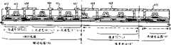
图7是一种用于在被照物体表面形成线状激光束的光学系统的构造的实施例。该种结构相当普通。以上所描述的所有光学系统均基于图7所示的结构。根据该结构,激光束的截面形状被转换成线状,同时激光束在被照表面上照射的能量密度分布变均匀。总之,用于使激光束能量密度均匀化的光学系统被称为束均质器。Fig. 7 is an example of the configuration of an optical system for forming a linear laser beam on the surface of an object to be irradiated. This structure is quite common. All optical systems described above are based on the structure shown in FIG. 7 . According to this structure, the cross-sectional shape of the laser beam is converted into a linear shape, and at the same time, the energy density distribution of the laser beam irradiation on the irradiated surface becomes uniform. In summary, an optical system for homogenizing the energy density of a laser beam is called a beam homogenizer.
由激光器71发射的激光束被一柱状透镜组73分成垂直于其传播方向的方向,由此决定线状激光束在垂直方向的长度。在本说明书中该方向被称为第一方向。假设当在光学系统中插入一面镜子,第一方向随着被镜子弯曲的光线方向而改变。在该结构中,柱状透镜阵列被分成七部分。然后通过柱状透镜74在被照物体表面合成激光束,由此使线状激光束在纵向的能量密度分布均匀化。The laser beam emitted by the laser 71 is divided into a direction perpendicular to its propagation direction by a cylindrical lens group 73, thereby determining the length of the linear laser beam in the vertical direction. This direction is referred to as a first direction in this specification. Suppose that when a mirror is inserted in the optical system, the first direction changes with the direction of the light rays bent by the mirror. In this structure, the lenticular lens array is divided into seven parts. Then, the laser beam is synthesized on the surface of the object to be irradiated by the lenticular lens 74, thereby uniformizing the energy density distribution of the linear laser beam in the longitudinal direction.
接着,将描述图7侧视图中所示的结构。由激光器71发射的激光束由透镜阵列72a和72a分成垂直其传播方向和第一方向的方向,由此决定线状激光束在宽度方向的长度。本说明书中该方向被称为第二方向。假设在光学系统中插入一面镜子,第二方向随着被镜子所弯曲的光线的方向而变化。在本结构中,柱状透镜阵列72a和72a分别被分成四部分。被分离的激光束暂由柱状透镜74合成。此后,激光束被镜77反射,然后被双重柱状透镜78聚焦,从而在被照射物体表面79再次形成单激光束。双重柱状透镜78由两个柱状透镜组成。这样激光束在宽度方向的均匀能量密度分布以及线状激光束在宽度方向的长度被确定。Next, the structure shown in the side view of FIG. 7 will be described. The laser beam emitted by the laser 71 is divided by lens arrays 72a and 72a into directions perpendicular to its propagation direction and the first direction, thereby determining the length of the linear laser beam in the width direction. This direction is referred to as a second direction in this specification. Assuming a mirror is inserted in the optical system, the second direction varies with the direction of the light rays bent by the mirror. In the present structure, the lenticular lens arrays 72a and 72a are divided into four, respectively. The split laser beams are temporarily synthesized by the lenticular lens 74 . Thereafter, the laser beam is reflected by the mirror 77 and then focused by the double lenticular lens 78 to form a single laser beam again on the surface 79 of the irradiated object. The double lenticular lens 78 is composed of two lenticular lenses. Thus the uniform energy density distribution of the laser beam in the width direction and the length of the linear laser beam in the width direction are determined.
例如,用作激光器71的是一种准分子激光器,其中激光器窗口的尺寸为10mm×30mm(分别为激光束断面宽度的一半),并且激光束由具有图7A和7B所示结构的光学系统所产生。由此,可在被照物体79表面得到具有均匀能量密度分布和尺寸为125mm×0.4mm的线状激光束。For example, what is used as the laser 71 is an excimer laser in which the size of the laser window is 10mm×30mm (half the cross-sectional width of the laser beam, respectively), and the laser beam is formed by an optical system having the structure shown in FIGS. 7A and 7B. produce. Thus, a linear laser beam having a uniform energy density distribution and a size of 125 mm×0.4 mm can be obtained on the surface of the object 79 to be irradiated.
此时,例如当以石英作为所有光学系统的基材时,可获得高传输率。注意优选对光学系统进行涂覆,这样在所用准分子激光器的频率下可获得99%或以上的传输率。Here, for example, when quartz is used as the base material for all optical systems, high transmission rates can be achieved. Note that the optical system is preferably coated such that a transmission rate of 99% or more is obtained at the frequency of the excimer laser used.
然后,用由上述结构形成的线状激光束在横向逐渐移动的同时重叠照射。这样,当对无定形半导体膜的整个表面进行激光退火处理时,无定形半导体膜可被晶化,其结晶性可被改善而获得结晶半导体膜,或可使杂质元素被激活。Then, the linear laser beam formed by the above-mentioned structure is overlapped and irradiated while gradually moving in the lateral direction. Thus, when the entire surface of the amorphous semiconductor film is subjected to laser annealing, the amorphous semiconductor film can be crystallized, its crystallinity can be improved to obtain a crystalline semiconductor film, or impurity elements can be activated.
发明内容Contents of the invention
然而如图7所示,用于形成线状激光束的光学系统很复杂。这样的光学系统存在的问题是很难进行光学调节,此外由于足迹(footprint)变大,器件被增大。However, as shown in FIG. 7, the optical system for forming a linear laser beam is complicated. The problem with such an optical system is that it is difficult to optically adjust, and in addition, the device is enlarged due to the larger footprint.
此外在使用相对被照射物体其反射率较高的激光束的情况下,当前述激光束垂直入射到被照物体时,产生所谓的返回光束,它以和光束入射到被照物体时相同的光路返回。返回光束成为对激光器输出和频率变化以及激光杆的破坏等有不利影响的因素。In addition, in the case of using a laser beam with a high reflectivity relative to the object to be irradiated, when the aforementioned laser beam is vertically incident on the object to be irradiated, a so-called return beam is generated, which takes the same optical path as when the beam is incident on the object to be irradiated. return. The return beam becomes a factor that adversely affects laser output and frequency changes, damage to the laser rod, and the like.
因此,本发明的一个目的是提供一种激光照射器件,其中通过使用比传统光学系统更简单的光学系统形成线状激光束,并且使用这样的线状激光束可更有效地进行退火处理,以及一种使用这种激光照射器件的激光照射方法。此外,本发明的另一个目的是提供一种半导体器件的制造方法,其操作步骤中包含前述激光照射方法。Accordingly, an object of the present invention is to provide a laser irradiation device in which a linear laser beam is formed by using an optical system simpler than conventional optical systems, and annealing treatment can be performed more efficiently using such a linear laser beam, and A laser irradiation method using such a laser irradiation device. Furthermore, another object of the present invention is to provide a method of manufacturing a semiconductor device, which includes the aforementioned laser irradiation method in its operating steps.
本发明的特征在于由相对于凸透镜倾斜入射的激光束产生诸如像散等像差,并且在照射表面或在其周围区域产生线状激光束。The present invention is characterized in that aberrations such as astigmatism are generated by a laser beam obliquely incident with respect to a convex lens, and that a linear laser beam is generated on an irradiated surface or in its surrounding area.
涉及在本说明书中公开的一种激光照射器件的本发明的结构的特征在于,它具有一个激光器和一个凸透镜,该凸透镜相对于前述激光器发射的激光束的传播方向倾斜设置并使照射表面上或其周围区域中的前述激光束的形状成为线状。The structure of the present invention relating to a laser irradiation device disclosed in this specification is characterized in that it has a laser and a convex lens which is arranged obliquely with respect to the propagation direction of the laser beam emitted by the aforementioned laser and makes the irradiation surface or The shape of the aforementioned laser beams in the surrounding area becomes linear.
另外,至于涉及激光照射器件的本发明的其它结构,它是一个具有激光器和凸透镜的激光照射器件,该凸透镜相对前述激光器发射的激光束的传播方向倾斜设置并使照射表面上或其周围区域中的前述激光束的形状成为线状形状,其特征如下:假定当激光器发射的激光通过前述凸透镜入射到基片上所形成的被照物体时所测得的激光束的宽度为w,而前述基片的厚度为d,前述激光束相对于前述被照射物体以满足如下公式的入射角θ入射:In addition, as for the other structure of the present invention related to the laser irradiation device, it is a laser irradiation device having a laser and a convex lens, the convex lens is arranged obliquely with respect to the propagation direction of the laser beam emitted by the aforementioned laser and makes the irradiation surface or its surrounding area The shape of the aforementioned laser beam becomes a linear shape, and its characteristics are as follows: Assuming that the laser beam emitted by the laser is incident on the object to be illuminated on the substrate through the aforementioned convex lens, the width of the measured laser beam is w, and the aforementioned substrate The thickness of is d, and the aforementioned laser beam is incident on the aforementioned object to be irradiated at an incident angle θ satisfying the following formula:
θ≥arctan(w/(2×d))θ≥arctan(w/(2×d))
在上述各个结构中,前述激光器的特征在于它是连续振荡或脉冲振荡的固态激光器、气体激光器或金属激光器。应该注意到作为前述固态激光器,列出了连续振荡或脉冲振荡的YAG激光器、YVO4激光器、YLF激光器、YAlO3激光器、玻璃激光器、红宝石激光器、金绿宝石激光器、Ti:蓝宝石激光器等;作为前述气体激光器,列出了连续振荡或脉冲振荡的准分子激光器、Ar激光器、Kr激光器、CO2激光器等,而作为前述金属激光器,列出氦-镉激光器、铜蒸汽激光器、金蒸汽激光器等。In each of the above structures, the aforementioned laser is characterized in that it is a continuous-oscillation or pulse-oscillation solid-state laser, a gas laser, or a metal laser. It should be noted that as the aforementioned solid-state lasers, continuous oscillation or pulse oscillation YAG lasers, YVO4 lasers, YLF lasers, YAlO3 lasers, glass lasers, ruby lasers, chrysoberyl lasers, Ti:sapphire lasers, etc. are listed; as the aforementioned As gas lasers, excimer lasers, Ar lasers, Kr lasers,CO2 lasers, etc., which are continuously oscillating or pulsed, are listed, and as the aforementioned metal lasers, helium-cadmium lasers, copper vapor lasers, gold vapor lasers, etc. are listed.
此外,在上述各个结构中,所希望的是前述激光束被一种非线性光学元件转化成高次谐波。例如,已知一种YAG激光器发射波长为1065nm的激光束作为基波。这种激光束相对于硅膜的吸收系数很低,因此如果保持其波长不变,从技术角度很难使半导体膜之一的非晶硅膜晶化。然而,采用非线性光学元件可使该激光束转变为较短波长,而作为高次谐波,列出了第二高次谐波(532nm)、第三高次谐波(355nm)、第四高次谐波(266nm)及第五高次谐波(213nm)。由于这些高次谐波相对于非晶硅膜具有高的吸收系数,它们可被用于非晶硅膜的晶化。Furthermore, in each of the above structures, it is desirable that the aforementioned laser beam is converted into higher harmonics by a nonlinear optical element. For example, it is known that a YAG laser emits a laser beam having a wavelength of 1065 nm as a fundamental wave. Such a laser beam has a low absorption coefficient with respect to a silicon film, so it is technically difficult to crystallize an amorphous silicon film, one of semiconductor films, if its wavelength is kept constant. However, this laser beam can be converted to a shorter wavelength by using a nonlinear optical element, and as higher harmonics, the second higher harmonic (532nm), the third higher harmonic (355nm), the fourth Higher harmonic (266nm) and fifth higher harmonic (213nm). Since these higher harmonics have high absorption coefficients relative to amorphous silicon films, they can be used for crystallization of amorphous silicon films.
此外,在上述各个结构中,前述凸透镜的特征在于它是一个非球面透镜。另外,作为凸透镜,列出了弯月形透镜、双凸透镜、平凸透镜等;而作为本发明的凸透镜,可以是这些透镜中的任意一种,并且激光束的入射表面可以是凸透镜两表面中任意一个。Furthermore, in each of the above structures, the aforementioned convex lens is characterized in that it is an aspherical lens. In addition, as the convex lens, meniscus lens, biconvex lens, plano-convex lens, etc. have been listed; and as the convex lens of the present invention, it can be any one of these lenses, and the incident surface of the laser beam can be any of the two surfaces of the convex lens. one.
此外,在上述结构中,对于前述基片,可采用玻璃基片、石英基片、硅基片、塑料基片、金属基片、不锈包层基片、柔性基片等。作为前述玻璃基片,可以是由钡硼硅酸盐玻璃、铝硼硅酸盐玻璃等构成的基片。此外,柔性基片指由PET、PES、PEN、丙烯酸树脂等构成的膜状基片,如果半导体基片采用柔性基片制备,可望减轻其重量。如果在柔性基片的表面上或在其表面和背面上,形成单层或多层由铝膜(AlON、AlN、AlO等)、碳膜(DLC(类金刚石碳)等)、SiN等构成的阻挡层,所希望的是可使耐久性等得到增强。Furthermore, in the above structure, for the aforementioned substrate, a glass substrate, a quartz substrate, a silicon substrate, a plastic substrate, a metal substrate, a stainless clad substrate, a flexible substrate, etc. can be used. As the aforementioned glass substrate, a substrate composed of barium borosilicate glass, aluminoborosilicate glass, or the like may be used. In addition, the flexible substrate refers to a film-like substrate made of PET, PES, PEN, acrylic resin, etc. If the semiconductor substrate is made of a flexible substrate, it is expected to reduce its weight. If on the surface of the flexible substrate or on its surface and back, a single layer or multilayers composed of aluminum film (AlON, AlN, AlO, etc.), carbon film (DLC (diamond-like carbon) etc.), SiN, etc. The barrier layer is desirable so that durability and the like can be enhanced.
此外,涉及本说明书中公开的激光照射方法的本发明的结构的特点在于,通过相对于激光束传播方向倾斜放置的凸透镜,在被照表面上或在其周围区域内形成线状光束,前述线状光束相对于被照物体相对移动进行照射。此外,涉及激光照射法的本发明的其它结构的特点在于,通过相对于激光束传播方向倾斜放置的凸透镜,在被照表面上或在其周围区域内形成线状光束。假定当前述线状光束入射到基片上所形成的被照物体时所测得的光束的宽度为w,而前述基片的厚度为d,前述线状光束以满足如下公式的入射角θ入射到被照物体:In addition, the structure of the present invention related to the laser irradiation method disclosed in this specification is characterized in that a linear beam is formed on the irradiated surface or in its surrounding area by a convex lens placed obliquely with respect to the propagation direction of the laser beam, the aforementioned line The light beam moves relative to the object to be irradiated. Furthermore, other structures of the present invention related to the laser irradiation method are characterized in that a linear beam is formed on the irradiated surface or in its surrounding area by means of a convex lens placed obliquely with respect to the direction of propagation of the laser beam. Assuming that the width of the light beam measured when the aforementioned linear beam is incident on the object to be irradiated on the substrate is w, and the thickness of the aforementioned substrate is d, the aforementioned linear beam satisfies the incident angle θ of the following formula and is incident on Illuminated object:
θ≥arctan(w/(2×d))并且前述线状光束相对于前述被照物体相对移动时前述线状光束进行照射。在上述各个结构中,前述激光器的特点在于它是固态激光器、气体激光器或是连续振荡或脉冲振荡的金属激光器。应该注意到作为前述固态激光器,列出了YAG激光器、YVO4激光器、YLF激光器、YAlO3激光器、玻璃激光器、红宝石激光器、金绿宝石激光器、连续振荡或脉冲振荡的Ti:蓝宝石激光器等;作为前述气体激光器,列出了准分子激光器、Ar激光器、Kr激光器、连续振荡或脉冲振荡的CO2激光器等,而作为前述金属激光器,列出氦-镉激光器、铜蒸汽激光器和金蒸汽激光器等。此外,在上述各个结构中,所希望的是前述激光束被一种非线性光学元件转化成高次谐波。此外,在上述各个结构中,前述凸透镜的特点在于它是一个非球面透镜。另外,作为凸透镜,有弯月形透镜、双凸透镜、平凸透镜等;而作为本发明的凸透镜,可以是这些透镜中的任意一种,并且激光束的入射表面可以是凸透镜两表面中任意一个。θ≧arctan (w/(2×d)) and the linear beam is irradiated when the linear beam moves relative to the object to be irradiated. In each of the above structures, the aforementioned laser is characterized in that it is a solid-state laser, a gas laser, or a continuous-oscillation or pulse-oscillation metal laser. It should be noted that as the aforementioned solid-state lasers, YAG lasers,YVO4 lasers, YLF lasers,YAlO3 lasers, glass lasers, ruby lasers, chrysoberyl lasers, continuous oscillation or pulse oscillation Ti:sapphire lasers, etc. are listed; as the aforementioned As gas lasers, excimer lasers, Ar lasers, Kr lasers, continuous oscillation or pulse oscillationCO2 lasers, etc. are listed, and as the aforementioned metal lasers, helium-cadmium lasers, copper vapor lasers, gold vapor lasers, etc. are listed. Furthermore, in each of the above structures, it is desirable that the aforementioned laser beam is converted into higher harmonics by a nonlinear optical element. Furthermore, in each of the above structures, the aforementioned convex lens is characterized in that it is an aspherical lens. In addition, as the convex lens, there are meniscus lens, biconvex lens, plano-convex lens, etc.; and as the convex lens of the present invention, it can be any one of these lenses, and the incident surface of the laser beam can be any one of the two surfaces of the convex lens.
此外,在上述结构中,对于前述基片,可采用玻璃基片、石英基片、硅基片、塑料基片、金属基片、不锈包层基片、柔性基片等。Furthermore, in the above structure, for the aforementioned substrate, a glass substrate, a quartz substrate, a silicon substrate, a plastic substrate, a metal substrate, a stainless clad substrate, a flexible substrate, etc. can be used.
此外,涉及本说明书中公开的制造半导体器件的方法的本发明的结构的特点在于,通过相对于激光束传播方向倾斜放置的凸透镜,在被照表面上或在其周围区域内形成线状光束,前述线状光束相对于半导体膜相对移动时前述线状光束进行照射。In addition, the structure of the present invention related to the method of manufacturing a semiconductor device disclosed in this specification is characterized in that a linear beam is formed on the irradiated surface or in its surrounding area by a convex lens placed obliquely with respect to the laser beam propagation direction, The said linear beam is irradiated when the said linear beam moves relatively with respect to a semiconductor film.
此外,涉及制造半导体器件的方法的本发明的其它结构的特点在于,通过相对于激光束传播方向倾斜放置的凸透镜,在被照表面上或在其周围区域内形成线状光束。假定当前述线状光束入射到基片上所形成的半导体膜时所测得的线状光束的宽度为w,而前述基片的厚度为d,前述线状光束相对于半导体膜以满足如下公式的入射角θ入射:Furthermore, other structures of the present invention relating to a method of manufacturing a semiconductor device are characterized in that a linear beam is formed on the irradiated surface or in its surrounding area by means of a convex lens placed obliquely with respect to the direction of propagation of the laser beam. Assuming that the width of the linear beam measured when the aforementioned linear beam is incident on the semiconductor film formed on the substrate is w, and the thickness of the aforementioned substrate is d, the aforementioned linear beam satisfies the following formula with respect to the semiconductor film Incident angle θ incident:
θ≥arctan(w/(2×d))并且前述线状光束进行照射同时前述线状光束相对于前述半导体膜移动。在上述各个结构中,前述激光束的特点在于它是固态激光器、气体激光器或连续振荡或脉冲振荡的金属激光器。应该注意作为前述固态激光器列出了YAG激光器、YVO4激光器、YLF激光器、YAlO3激光器、玻璃激光器、红宝石激光器、金绿宝石激光器、连续振荡或脉冲振荡的Ti:蓝宝石激光器等;作为前述气体激光器,列出了准分子激光器、Ar激光器、Kr激光器、连续振荡或脉冲振荡的CO2激光器等,而作为前述金属激光器,列出氦-镉激光器、铜蒸汽激光器和金蒸汽激光器等。此外,在上述各个结构中,所希望的是前述激光束被一种非线性光学元件转化成高次谐波。此外,在上述各个结构中,前述凸透镜的特点在于它是一个非球面透镜。另外,作为凸透镜,有弯月形透镜、双凸透镜、平凸透镜等;而作为本发明的凸透镜,可以是这些透镜中的任意一种,并且激光束的入射表面可以是凸透镜两表面中任意一个。θ≧arctan (w/(2×d)) and the aforementioned linear beam is irradiated while the aforementioned linear beam moves relative to the aforementioned semiconductor film. In each of the above structures, the aforementioned laser beam is characterized in that it is a solid-state laser, a gas laser, or a continuous-oscillation or pulse-oscillation metal laser. It should be noted that as the aforementioned solid-state lasers, YAG lasers,YVO4 lasers, YLF lasers,YAlO3 lasers, glass lasers, ruby lasers, chrysoberyl lasers, continuous oscillation or pulse oscillation Ti:sapphire lasers, etc. are listed; as the aforementioned gas lasers , excimer lasers, Ar lasers, Kr lasers, continuous oscillation or pulse oscillationCO lasers, etc. are listed, while as the aforementioned metal lasers, helium-cadmium lasers, copper vapor lasers, and gold vapor lasers, etc. are listed. Furthermore, in each of the above structures, it is desirable that the aforementioned laser beam is converted into higher harmonics by a nonlinear optical element. Furthermore, in each of the above structures, the aforementioned convex lens is characterized in that it is an aspheric lens. In addition, as the convex lens, there are meniscus lens, biconvex lens, plano-convex lens, etc.; and as the convex lens of the present invention, it can be any one of these lenses, and the incident surface of the laser beam can be any one of the two surfaces of the convex lens.
此外,在上述结构中,对于前述基片,可采用玻璃基片、石英基片、硅基片、塑料基片、金属基片、不锈包层基片、柔性基片等。Furthermore, in the above structure, for the aforementioned substrate, a glass substrate, a quartz substrate, a silicon substrate, a plastic substrate, a metal substrate, a stainless clad substrate, a flexible substrate, etc. can be used.
在各个结构中,前述半导体膜为含硅膜是所希望的。由于本发明具有非常简化的结构,光调节容易,并且器件尺寸缩小。此外,即使在使用多个激光光束进行照射的情况下,由于光学系统简化,能轻易使所有激光束具有相同形状。为了进行均匀的退火处理,使多个激光束保持相同形状是很重要的。如果使用这样的多个激光束,当光束照射到具有大面积的基片时,能够提高生产能力。此外,可使用通过合成多个激光器的光束。再者,本发明中由于激光束相对于被照射体倾斜入射,可防止返回光束,由于不需设置隔离物,使结构更加简化。因此,可降低成本。另外,对于基片上形成的半导体膜能够进行有效照射,并且采用这样的半导体有可能使所制备的TFT电性能的变化减小。从而也可能使用这样的TFT制备的半导体的操作性能和可靠性得到增加。In each structure, it is desirable that the aforementioned semiconductor film is a silicon-containing film. Since the present invention has a very simplified structure, light adjustment is easy, and the device size is reduced. Furthermore, even in the case of irradiation using a plurality of laser beams, all the laser beams can be easily made to have the same shape due to the simplification of the optical system. For uniform annealing, it is important to maintain the same shape of the multiple laser beams. If such a plurality of laser beams are used, when the beams are irradiated to a substrate having a large area, throughput can be improved. In addition, beams by combining multiple lasers can be used. Furthermore, in the present invention, since the laser beam is incident obliquely relative to the irradiated body, return beams can be prevented, and the structure is simplified because no spacer is required. Therefore, costs can be reduced. In addition, the semiconductor film formed on the substrate can be effectively irradiated, and the use of such a semiconductor may reduce the change in the electrical properties of the prepared TFT. It is thus also possible to increase the operational performance and reliability of semiconductors produced using such TFTs.
附图说明Description of drawings
附图中:In the attached picture:
图1是示出本发明的光学系统的实例的示图;FIG. 1 is a diagram showing an example of an optical system of the present invention;
图2是示出相对于被照物体获得激光束入射角θ的示图;FIG. 2 is a diagram illustrating obtaining an incident angle θ of a laser beam with respect to an object to be irradiated;
图3是示出根据本发明在照射表面上形成的激光束的形状的实例示图;3 is a diagram showing an example of the shape of a laser beam formed on an irradiated surface according to the present invention;
图4是示出在使用多个激光束的情况下本发明的一个光学系统的实例示图;Fig. 4 is a diagram showing an example of an optical system of the present invention in the case of using a plurality of laser beams;
图5是示出在使用多个激光束的情况下本发明的一个光学系统的实例示图;5 is a diagram showing an example of an optical system of the present invention in the case of using a plurality of laser beams;
图6是示出在使用多个激光束的情况下本发明的一个光学系统的实例示图;6 is a diagram showing an example of an optical system of the present invention in the case of using a plurality of laser beams;
图7是示出一个传统光学系统的实例示图;Fig. 7 is a diagram showing an example of a conventional optical system;
图8A到8C是用于解释一种像素TFT和一种用于驱动电路的TFT的制造步骤的横截面图;8A to 8C are cross-sectional views for explaining manufacturing steps of a pixel TFT and a TFT for a driver circuit;
图9A到9C是用于解释一种像素TFT和一种用于驱动电路的TFT的制造步骤的横截面图;9A to 9C are cross-sectional views for explaining manufacturing steps of a pixel TFT and a TFT for a driver circuit;
图10是用于解释一种像素TFT和一种用于驱动电路的TFT的制造步骤的横截面图;10 is a cross-sectional view for explaining manufacturing steps of a pixel TFT and a TFT for a driver circuit;
图11是用于解释像素TFT结构的俯视图;11 is a top view for explaining the structure of a pixel TFT;
图12是一种有源矩阵型液晶显示器件的横截面图;12 is a cross-sectional view of an active matrix liquid crystal display device;
图13是一种发光器件的驱动电路和像素部分的横截面结构示图;Fig. 13 is a cross-sectional structural diagram of a driving circuit and a pixel portion of a light emitting device;
图14A到14F是示出半导体器件实例的示图;14A to 14F are diagrams showing examples of semiconductor devices;
图15A到15D是示出半导体器件实例的示图;15A to 15D are diagrams showing examples of semiconductor devices;
图16A到16C是示出半导体器件实例的示图;16A to 16C are diagrams showing examples of semiconductor devices;
图17是示出利用本发明进行半导体膜晶化操作和通过SEM观察半导体膜的实例示图;17 is a diagram showing an example of crystallization operation of a semiconductor film and observation of the semiconductor film by SEM using the present invention;
图18是示出利用本发明进行半导体膜晶化操作和通过SEM观察半导体膜的实例示图;18 is a diagram showing an example of crystallization operation of a semiconductor film and observation of the semiconductor film by SEM using the present invention;
图19A到19H是示出利用本发明制造TFT的实例示图;19A to 19H are diagrams showing an example of manufacturing a TFT using the present invention;
图20A到20B是示出利用本发明制造TFT并测量电性能的实例示图;20A to 20B are diagrams showing an example of manufacturing a TFT and measuring electrical properties using the present invention;
图21A到21C是示出利用本发明制造TFT的实例示图;21A to 21C are diagrams showing examples of manufacturing TFTs utilizing the present invention;
图22A到22B是示出利用本发明制造TFT并测量电性能的实例示图;22A to 22B are diagrams showing an example of manufacturing a TFT and measuring electrical properties using the present invention;
图23A到23B是示出利用本发明制造TFT并测量电性能的实例示图;以及23A to 23B are diagrams showing an example of manufacturing a TFT and measuring electrical properties using the present invention; and
图24示出本发明的光学系统实例的示图;Figure 24 shows a diagram of an example of an optical system of the present invention;
图25A到25C是示出TFT的ID-VG性能和对沟道长度依赖关系的曲线图,该TFT在晶化过程中通过将激光束照射和使用具有催化作用的镍的热结晶法结合起来制造的;25A to 25C are graphs showing the ID-VG performance and the dependence on the channel length of TFTs manufactured by combining laser beam irradiation and thermal crystallization using nickel having a catalytic effect in the crystallization process of;
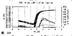
图26A到26C是示出在晶化过程中使用激光束照射制造的TFT的ID-VG性能和对沟道长度依赖关系的曲线图;26A to 26C are graphs showing the ID-VG performance of TFTs manufactured using laser beam irradiation during crystallization and the dependence on channel length;
图27是示出完全抑制型膜厚为66nm的TFT的ID-VG性能的曲线图;FIG. 27 is a graph showing the ID-VG performance of a completely suppressed TFT with a film thickness of 66 nm;
图28是示出部分耗尽型膜厚为150nm的TFT的ID-VG性能的曲线图。FIG. 28 is a graph showing ID-VG performance of a partially depleted TFT having a film thickness of 150 nm.
具体实施方式Detailed ways
实施例模式Example mode
在本发明实施例模式中,以下将参考图1和图2描述形成线状光束的方法。In an embodiment mode of the present invention, a method of forming a linear beam will be described below with reference to FIGS. 1 and 2 .
由激光器101发射的激光束通过镜面(mirror)102入射进入凸透镜103。此处,作为激光器101,使用固态激光器、气体激光器或连续振荡或脉冲振荡的金属激光器。应该注意作为前述固态激光器,列出了YAG激光器、YVO4激光器、YLF激光器、YAlO3激光器、玻璃激光器、红宝石激光器、金绿宝石激光器、Ti:蓝宝石激光器等;作为前述气体激光器,列出了准分子激光器、Ar激光器、Kr激光器、连续振荡或脉冲振荡的CO2激光器等,而作为前述金属激光器,列出氦-镉激光器、铜蒸汽激光器、金蒸汽激光器等。然后,来自激光器101的振荡激光通过一个非线性元件可被转化成高次谐波。此外,在激光器101和镜面102之间或在镜面102和凸透镜103之间放置扩展器,分别在较长方向和较短向将光束扩展至所希望尺寸。光束扩展器在激光器发射的激光束的形状很小的情况下尤其有效。此外,可不放置镜面,或可放置多个镜面。A laser beam emitted by a
激光束相对于凸透镜103倾斜入射。通过以此方式入射,由于诸如像散的像差聚焦位置被移动,可在被照表面或其周围区域内形成线状光束106。应该注意,如果凸透镜103由合成石英玻璃构成,是所希望的,因为获得高透明度。此外,对于凸透镜103表面提供的涂层,所希望的是使用相对于所使用激光束的波长能够获得99%或更高的透明度的涂层。另外,对于凸透镜,使用其球面透镜像差被修正的非球面透镜。如果使用非球面透镜,聚光性能增加,并且长宽比和能量密度分布也被增加。The laser beam is obliquely incident on the
然后,当如此形成的线状光束106照射时,例如,它能通过相对于被照体104相对移动,例如在参考数字107所示方向或参考数字108、109所示方向移动,而照射被照体104的所希望区域或整个区域。“相对移动”实际上是指“操作置于台面上的被照体”。Then, when the thus formed linear
然而,根据激光束的波长,被照体表面上的反射光束和其上形成被照体104的基片105的背面的反射光束间可能出现相互干扰。图2中,作为被照体104,显示了一个实例。其中在基片10上形成半导体11。如果半导体膜11表面上的反射束14和基片10背面的反射束13没有重叠,不会发生由于这些光束的干扰。However, depending on the wavelength of the laser beam, mutual interference may occur between the reflected beam on the surface of the object and the reflected beam on the back surface of the
在此情况下,当一个垂直于被照表面且它是包含假定为长光束的长方形的长边或短边的平面之一的平面被定义为入射面,激光束的入射角满足θ≥arctan(W/2d)是所希望的,其中W为包含于入射表面的长边或短边的长度,d为相对于激光束透明的基片的厚度。该W为W=(W1+W2)/2,此时W1是入射到被照表面的激光束的长度15,W2是从基片10的后表面反射回来的激光束的长度。应注意,当入射表面上不存在激光束的轨迹,入射表面上的投影轨迹入射角被定义为θ。如果激光束以入射角θ入射,基片表面上的被反射光束不与来自基片背面的反射光束干涉,从而使激光束均匀照射。更进一步,通过设定在被照体表面的入射角为Brewster角,反射率减至最小而能够使激光束被有效利用。在上面,基片的折射率为1。实际中,多数基片的折射率为1.5。当考虑此值时,得到大于上面计算所得角度的计算值。然而,因为线状激光束的长度方向的两边的能量被衰减,在这部分干扰影响很小,并且对于上述计算值可得到充分的干扰弱化效果。In this case, when a plane perpendicular to the illuminated surface and it is one of the planes containing the long side or short side of the rectangle assumed to be the long beam is defined as the incident plane, the incident angle of the laser beam satisfies θ ≥ arctan( W/2d) is desirable, where W is the length of the long side or short side included in the incident surface, and d is the thickness of the substrate transparent to the laser beam. The W is W=(W1 +W2 )/2, where W1 is the
此外,可在被照体表面形成防止反射膜。In addition, an anti-reflection film can be formed on the surface of the object to be irradiated.
当采用这样的激光照射器件进行半导体膜的退火处理,相应的半导体膜可被晶化,通过增强结晶性可得到结晶半导体并可进行杂质元素的激活。When annealing of a semiconductor film is performed using such a laser irradiation device, the corresponding semiconductor film can be crystallized, a crystalline semiconductor can be obtained by enhancing crystallinity and activation of impurity elements can be performed.
应该注意激光束的形状根据激光器发射激光的种类而不同,即使激光束由光学系统形成,它也易受原始形状的影响并很容易随其改变。例如,由XeCl准分子激光器发射的激光束的形状为长方形,而对于固态激光器发射的激光束的形状,如果杆的形状为柱状,则变为环状,而如果为平板状,则变为长方形。本发明可适用于任何形状。It should be noted that the shape of the laser beam differs depending on the type of laser light emitted from the laser, and that even if the laser beam is formed by an optical system, it is susceptible to the original shape and easily changed therewith. For example, the shape of the laser beam emitted by the XeCl excimer laser is rectangular, while for the shape of the laser beam emitted by the solid-state laser, if the shape of the rod is columnar, it becomes circular, and if it is flat, it becomes rectangular . The invention is applicable to any shape.
包含上述结构的本发明将通过以下所示实施例进一步描述。The present invention comprising the above structures will be further described by the Examples shown below.
实施例Example
实施例1Example 1
本实施例中,将参考下面图1和图3描述其中由本发明形成线性激光束的实例。In this embodiment, an example in which a linear laser beam is formed by the present invention will be described with reference to FIGS. 1 and 3 below.
作为激光器101,使用YAG激光器。假定来自激光器101的振荡激光束被一个包含于激光器101中的非线性光学元件转换成第二高次谐波,此时,假设激光束处于TEMoo模式,并具有2.25mm的束直径和0.35mrad的扩展角。As the
随后,激光束相对于具有20mm焦长的凸透镜103以20度的入射角φ入射。然后,在本实施例中,对在平行于凸透镜放置的被照表面上形成的激光束的形状进行模拟。结果示于图3。由图3,可以明白在被照表面形成了长420μm、宽40μm的线状激光束。此外,线状激光束的能量分布为高斯分布。Subsequently, the laser beam is incident at an incident angle φ of 20 degrees with respect to the
从模拟结果,可以证实根据本发明在被照表面或在其周围区域形成了线状激光束。然后,当使用这样的激光照射器件对半导体膜进行退火处理时,相应的半导体膜可被晶化,通过增强结晶性获得结晶半导体膜,并且可进行杂质的激活。From the simulation results, it can be confirmed that a linear laser beam is formed on the irradiated surface or in its surrounding area according to the present invention. Then, when the semiconductor film is annealed using such a laser irradiation device, the corresponding semiconductor film can be crystallized, a crystalline semiconductor film is obtained by enhancing crystallinity, and activation of impurities can be performed.
实施例2Example 2
在本实施例中,将参考图4描述一个实例,其中激光束的照射是采用多个激光束进行的。作为111a~111c激光器,采用YAG激光器,这些激光束被一非线性光学元件转换成第二高次谐波。然后,当由激光器111a~111c发射的各激光束穿过镜面112a~112c后,这些激光束相对于凸透镜113a~113c倾斜入射。通过倾斜入射,由于诸如像散等像差聚焦位置被移动,在被照表面或其周围区域形成线状光束。此外,作为凸透镜,使用非球面透镜是所希望的。应该注意,在激光器111a~111c和镜面112a~112c之间或在镜面112a~112c和凸透镜113a~113c之间放置光束扩展器,而将光束的纵向和横向分别扩展至所希望尺寸。此外,可不放置镜面,或可放置多个镜面。In this embodiment, an example in which irradiation of a laser beam is performed using a plurality of laser beams will be described with reference to FIG. 4 . As the 111a-111c lasers, YAG lasers are used, and these laser beams are converted into second higher harmonics by a nonlinear optical element. Then, when the laser beams emitted by the
然后,当由此形成的线状激光束照射时,通过相对于被照体104相对移动,例如在参考数字107所示方向或参考数字108、109所示方向移动,能够照到被照体的所希望区域或整个区域。Then, when the thus formed linear laser beam is irradiated, by moving relative to the subject 104, for example, moving in the direction shown by
由于在本发明中,形成线状光束的光学系统具有非常简单的结构,很容易使多个激光束在被照表面形成具有相同形状的线状激光束。因此,由于用任意线状激光束照射任意表面进行相同退火处理,被照体的整个表面达到具有均匀物理性能并且生产能力提高。Since in the present invention, the optical system for forming a linear beam has a very simple structure, it is easy to make a plurality of laser beams form a linear laser beam having the same shape on the irradiated surface. Therefore, since an arbitrary surface is irradiated with an arbitrary linear laser beam to perform the same annealing treatment, the entire surface of the object to be irradiated is achieved to have uniform physical properties and productivity is improved.
应该注意本发明中,虽然举例说明了使用三个激光器的光束的实例,但激光器的数量不限于此,并且可不使用同类激光器。例如,也可能使用多个不同的激光器,所希望的区域由所希望的激光器照射,形成具有不同物理性能的半导体膜和在同一基片上制备具有不同性能的TFT。It should be noted that in the present invention, although an example using beams of three lasers is exemplified, the number of lasers is not limited thereto, and lasers of the same type may not be used. For example, it is also possible to use a plurality of different lasers, irradiate desired regions with desired lasers, form semiconductor films with different physical properties and fabricate TFTs with different properties on the same substrate.
实施例3Example 3
在本实施例中,以下参考图5描述一个实施,其中使用多个激光器从被照体的两侧进行激光束照射。In this embodiment, an implementation in which laser beam irradiation is performed from both sides of the subject using a plurality of lasers is described below with reference to FIG. 5 .
作为激光器121a、121b,采用连续振荡的YVO4激光器,通过非线性光学元件激光束被转换成第二高次谐波。然后,当由激光器121a、121b发射的各个激光束穿过镜面122a、122b后,相对于凸透镜123a、123b倾斜入射。通过倾斜入射,由于诸如像散等像差聚焦位置被移动,在被照表面或其周围区域形成线状光束。此外,作为凸透镜,使用非球面透镜是所希望的。As the lasers 121a and 121b, continuous oscillation YVO4 lasers are used, and laser beams are converted into second harmonics by nonlinear optical elements. Then, when the respective laser beams emitted by the lasers 121a, 121b pass through the mirrors 122a, 122b, they are obliquely incident on the convex lenses 123a, 123b. By oblique incidence, the focus position is shifted due to aberrations such as astigmatism, and a linear beam is formed on the irradiated surface or its surrounding area. In addition, as the convex lens, it is desirable to use an aspheric lens.
应该注意,在激光器121a、121b和镜面122a、122b之间或在镜面122a、122b和凸透镜123a、123b之间放置光束扩展器,而将光束的纵向和横向分别扩展至所希望尺寸。此外,可不放镜面,或可放置多个镜面。It should be noted that a beam expander is placed between the lasers 121a, 121b and the mirrors 122a, 122b or between the mirrors 122a, 122b and the convex lenses 123a, 123b to expand the longitudinal and lateral directions of the beam to the desired size respectively. Furthermore, no mirrors may be placed, or multiple mirrors may be placed.
然后,当由此形成的线状激光束照射时,通过相对于被照体104相对移动,例如在参考数字107所示方向或参考数字108、109所示方向移动,能够照到被照体104的所希望区域或整个区域。Then, when the linear laser beam thus formed is irradiated, the subject 104 can be irradiated by moving relative to the subject 104, for example, moving in the direction shown by
由于在本发明中,形成线状光束的光学系统具有非常简单的结构,很容易使多个激光束在被照表面形成具有相同形状的线状激光束。因此,多个激光束很容易彼此叠加。即使在根据被照体使用具有较低输出的激光器情况下,根据本实施例它完全能够适用。Since in the present invention, the optical system for forming a linear beam has a very simple structure, it is easy to make a plurality of laser beams form a linear laser beam having the same shape on the irradiated surface. Therefore, multiple laser beams are easily superimposed on each other. Even in the case of using a laser with a lower output depending on the subject, it is fully applicable according to the present embodiment.
应该注意在本发明中,虽然举例说明了使用两个激光器的光束的实例。但激光器的数量不限于此,并且可使用不同种类激光器。It should be noted that in the present invention, although an example using beams of two lasers is exemplified. But the number of lasers is not limited thereto, and different kinds of lasers may be used.
此外本实施例可与实施例2结合进行。In addition, this embodiment can be carried out in combination with
实施例4Example 4
本实施例中,将参考图6描述一个实例,其中通过采用多个激光器并将光束在被照体表面叠加进行照射。In this embodiment, an example will be described with reference to FIG. 6 in which irradiation is performed by using a plurality of lasers and superimposing beams on the surface of the subject.
作为激光器131a、131b,采用连续振荡的YLF激光器,通过非线性光学元件激光束被转换成第三高次谐波。然后,当由激光器131a、131b发射的各个激光束之后相对于凸透镜133a、133b倾斜入射。通过倾斜入射,由于诸如像散等像差聚焦位置被移动,在被照表面或其周围区域形成线状光束。此外,作为凸透镜,使用非球面透镜是所希望的。As the lasers 131a and 131b, continuous oscillation YLF lasers are used, and laser beams are converted into third harmonics by nonlinear optical elements. Then, when the respective laser beams emitted by the lasers 131a, 131b are then obliquely incident with respect to the convex lenses 133a, 133b. By oblique incidence, the focus position is shifted due to aberrations such as astigmatism, and a linear beam is formed on the irradiated surface or its surrounding area. In addition, as the convex lens, it is desirable to use an aspheric lens.
应该注意,在激光器131a、131b和凸透镜133a、133b之间放置光束扩展器,而将光束的较长方向和较短方向分别扩展至所希望尺寸。此外,可不放置镜面,或可放置多个镜面。It should be noted that beam expanders are placed between the lasers 131a, 131b and the convex lenses 133a, 133b to expand the longer and shorter directions of the beams to desired sizes, respectively. Also, no mirrors may be placed, or multiple mirrors may be placed.
然后,当由此形成的线状激光束照射时,通过相对于被照体104相对移动,例如在参考数字107所示方向或参考数字108、109所示方向移动,能够照到被照体104的所希望区域或整个区域。Then, when the linear laser beam thus formed is irradiated, the subject 104 can be irradiated by moving relative to the subject 104, for example, moving in the direction shown by
由于在本发明中,形成线状光束的光学系统具有非常简单的结构,很容易使多个激光束在被照表面形成具有相同形状的线状激光束。因此,多个激光束很容易彼此叠加。即使在根据被照体使用具有较低输出的激光器情况下,根据本实施例它完全能够适用。Since in the present invention, the optical system for forming a linear beam has a very simple structure, it is easy to make a plurality of laser beams form a linear laser beam having the same shape on the irradiated surface. Therefore, multiple laser beams are easily superimposed on each other. Even in the case of using a laser with a lower output depending on the subject, it is fully applicable according to the present embodiment.
应该注意本发明中,虽然举例说明了使用两个激光器的光束的实例。但激光器的数量不限于此,并且可使用不同种类激光器。此外,虽然激光束在被照表面被合成,但合成后,可通过光学系统形成线状光束。It should be noted that in the present invention, although an example using beams of two lasers has been exemplified. But the number of lasers is not limited thereto, and different kinds of lasers may be used. In addition, although the laser beams are synthesized on the surface to be irradiated, after the synthesis, a linear beam can be formed by the optical system.
此外本实施例可与实施例2或3自由结合。In addition, this embodiment can be freely combined with
实施例5Example 5
在本实施例中利用图8~11解释一种有源矩阵型基片的制造方法。为方便起见,一种其上共同形成CMOS电路、驱动电路,以及具有TFT像素和一定容积(hoding capacity)的像素部分的基片称为有源矩阵型基片。In this embodiment, a method of manufacturing an active matrix type substrate is explained using Figs. 8 to 11. For convenience, a substrate on which a CMOS circuit, a driver circuit, and a pixel portion having a TFT pixel and a hoding capacity are collectively formed is called an active matrix type substrate.
图8A示出基底膜的形成、半导体层的形成、绝缘膜的形成、第一导电膜和第二导电膜的形成。FIG. 8A shows formation of a base film, formation of a semiconductor layer, formation of an insulating film, formation of a first conductive film and a second conductive film.
首先,在本实施例中使用由玻璃如钡硼硅酸盐玻璃或铝硼硅酸盐玻璃构成的基片400。注意石英基片、硅基片、金属基片,以及在其基片表面形成绝缘膜的不锈钢基片也可作为基片400。另外,具有能够承受本实施例中使用的处理温度的热阻性能的塑料基片也可使用。由于本发明可容易的形成能量均匀分布的线性激光束,可能通过使用多个线性激光束有效地处理大面积基片。First, a
其次,利用已知方法,在基片400上形成由绝缘膜如氧化硅膜、氮化硅膜,或氮氧化硅膜构成的基底膜401。本实施例中,基底膜401采用双层结构,但也可使用上述单层绝缘膜,也可使用两层以上膜叠加的结构。Next, a
其次,在基底膜上形成半导体层。首先,通过已知方法(如溅射法、LPCVD法,和等离子体CVD法)形成厚度为25~200nm(优选30~150nm)的半导体膜。然后,通过激光晶化法将半导体膜晶化。作为激光晶化法,通过应用实施例1~4任意一种方法或实施例1~4任意一种方法的结合,对半导体膜激光束照射。优选使用连续或脉冲振荡固态激光器、气体激光器,或金属激光器。注意,作为固态激光器,可有YAG激光器、YVO4激光器、YLF激光器、YAlO3激光器、玻璃激光器、红宝石激光器、金绿宝石激光器、Ti:蓝宝石激光器等。作为气体激光器,可有连续振荡或脉冲振荡的准分子激光器、Ar激光器、Kr激光器、CO2激光器等。而作为金属激光器,可有氦-镉激光器、铜蒸汽激光器,或金蒸汽激光器。当然,不仅激光晶化法其它任何已知的晶化法(RTA,利用电炉退火的热晶化法,利用促进晶化的金属元素的热晶化法)也可结合使用。半导体膜可能是一种无定形半导体膜、微结晶半导体膜或一种结晶半导体膜。或者,半导体膜可以是具有无定形结构的化合物半导体膜,如非晶硅锗膜。Next, a semiconductor layer is formed on the base film. First, a semiconductor film is formed to a thickness of 25 to 200 nm (preferably 30 to 150 nm) by known methods such as sputtering, LPCVD, and plasma CVD. Then, the semiconductor film is crystallized by a laser crystallization method. As the laser crystallization method, by applying any one of the methods of Embodiments 1 to 4 or a combination of any one of the methods of Embodiments 1 to 4, the semiconductor film is irradiated with a laser beam. It is preferable to use a continuous or pulse-oscillated solid-state laser, a gas laser, or a metal laser. Note that, as a solid-state laser, there may be a YAG laser, a YVO4 laser, a YLF laser, a YAlO3 laser, a glass laser, a ruby laser, a chrysoberyl laser, a Ti:sapphire laser, or the like. As the gas laser, there are excimer lasers, Ar lasers, Kr lasers, CO2 lasers, etc. which are continuously oscillating or pulse oscillating. And as the metal laser, there may be a helium-cadmium laser, a copper vapor laser, or a gold vapor laser. Of course, not only the laser crystallization method but also any known crystallization method (RTA, thermal crystallization method using electric furnace annealing, thermal crystallization method using a crystallization-promoting metal element) can also be used in combination. The semiconductor film may be an amorphous semiconductor film, a microcrystalline semiconductor film or a crystalline semiconductor film. Alternatively, the semiconductor film may be a compound semiconductor film having an amorphous structure, such as an amorphous silicon germanium film.
在本实施例中,使用等离子体CVD法形成厚50nm的非晶硅膜,然后对该非晶硅膜使用利用促进晶化的金属元素的热晶化法和激光晶化法。镍被用作金属元素,并通过溶液涂层法被导入非晶硅膜。然后进行500℃、5小时的热处理,由此获得第一结晶硅膜。随后,由输出为10w的连续振荡YVO4激光器发射的激光束被非线性光学元件转换成第二高次谐波,以及然后由实施例1~4所示的光学系统之一或由组合这些实施例形成的光学系统形成线状激光束并照射,由此获得第二结晶硅膜。照射激光束到第一结晶硅膜,并将第一结晶硅膜改变为第二结晶硅膜改善第二结晶硅膜的结晶性。此刻,必需约0.01~100MW/cm2(优选0.1~10MW/cm2)能量密度。台面被以0.5~2000cm/s的速度相对移动到激光束,激光束照射,然后形成结晶硅膜。当使用脉冲振荡的准分子激光器,优选300Hz频率和100~1000mj/cm2(典型值为200~800mj/cm2)的激光能量密度。此刻,激光束可能重迭50~98%。In this embodiment, an amorphous silicon film having a thickness of 50 nm was formed using plasma CVD, and then thermal crystallization and laser crystallization using metal elements that promote crystallization were applied to the amorphous silicon film. Nickel was used as a metal element, and was introduced into the amorphous silicon film by a solution coating method. Thereafter, heat treatment was performed at 500° C. for 5 hours, whereby a first crystalline silicon film was obtained. Subsequently, the laser beam emitted by the continuous oscillation YVO4 laser with an output of 10w is converted into a second higher harmonic wave by a nonlinear optical element, and then implemented by one of the optical systems shown in Embodiments 1 to 4 or by a combination of these The optical system formed as an example forms and irradiates a linear laser beam, thereby obtaining a second crystalline silicon film. Irradiating the laser beam to the first crystalline silicon film and changing the first crystalline silicon film to the second crystalline silicon film improves the crystallinity of the second crystalline silicon film. At this point, an energy density of about 0.01 to 100 MW/cm2 (preferably 0.1 to 10 MW/cm2 ) is necessary. The mesa is relatively moved to the laser beam at a speed of 0.5 to 2000 cm/s, irradiated with the laser beam, and then a crystalline silicon film is formed. When a pulsed excimer laser is used, a frequency of 300 Hz and a laser energy density of 100-1000 mj/cm2 (typically 200-800 mj/cm2 ) are preferred. At this point, the laser beams may overlap by 50-98%.
当然,虽然可通过使用第一结晶硅膜形成TFT,由于第二结晶膜具有改善的结晶性,并且TFT的电性能被改善,因此优先使用第二结晶膜形成TFT。例如,虽然,当通过使用第一结晶膜形成TFT时,迁移率几乎是300cm2/Vs,但当使用第二结晶膜时,迁移率大大提高约为500~600cm2/Vs。Of course, although a TFT can be formed by using the first crystalline silicon film, since the second crystalline film has improved crystallinity and the electrical properties of the TFT are improved, it is preferable to form a TFT using the second crystalline film. For example, although, when a TFT is formed by using the first crystalline film, the mobility is almost 300 cm2 /Vs, but when the second crystalline film is used, the mobility is greatly improved by about 500 to 600 cm2 /Vs.
利用光刻方法通过在所得半导体膜上进行图形化处理形成半导体层402~406。The semiconductor layers 402 to 406 are formed by patterning the resulting semiconductor film by photolithography.
为控制TFT的阈值,在形成半导体层402~406后,可进行少量杂质元素(硼或磷)的掺杂。In order to control the threshold of the TFT, after forming the semiconductor layers 402-406, a small amount of impurity element (boron or phosphorus) can be doped.
其次形成栅绝缘膜407,覆盖半导体层402~406。栅绝缘膜407是利用等离子体CVD或溅射由厚40~150nm的含硅绝缘膜形成的。本实施例中,膜厚度为110nm的氮氧化硅膜通过等离子体CVD方法形成。栅绝缘膜当然不限于氮氧化硅膜,并且在单层或叠层结构中可使用其它含硅绝缘膜。Next, a gate insulating film 407 is formed to cover the semiconductor layers 402-406. The gate insulating film 407 is formed of an insulating film containing silicon with a thickness of 40 to 150 nm by plasma CVD or sputtering. In this embodiment, a silicon oxynitride film having a film thickness of 110 nm was formed by the plasma CVD method. The gate insulating film is of course not limited to a silicon oxynitride film, and other silicon-containing insulating films may be used in a single-layer or stacked-layer structure.
此外,如果使用氧化硅膜,可通过等离子体CVD法采用TEOS(原硅酸四乙酯)和O2混合物、反应压力40Pa,基片温度定为300~400℃形成,以及通过在0.5~0.8w/cm2的高频(13.56MHz)电功率密度下放电形成。通过随后对如此制造的氧化硅膜进行400~500℃的热退火处理,可获得高性能栅绝缘膜。In addition, if a silicon oxide film is used, it can be formed by plasma CVD method using a mixture of TEOS (tetraethyl orthosilicate) and O2 , a reaction pressure of 40Pa, and a substrate temperature of 300-400°C, and can be formed at a temperature of 0.5-0.8 Discharge formation under high frequency (13.56MHz) electric power density of w/cm2 . A high-performance gate insulating film can be obtained by subsequently subjecting the silicon oxide film thus produced to thermal annealing at 400 to 500°C.
然后厚20~100nm的第一导电膜408,以及厚100~400nm的第二导电膜409形成并被层叠在栅绝缘膜407上。在本实施例中由膜厚30nm的TaN膜构成的第一导电膜408,和由厚370nm的W膜构成的第二导电膜409被形成并层叠。TaN膜由溅射形成,并且Ta靶的溅射在氮气氛下进行。此外,W膜利用W靶溅射形成。另外,W膜也可利用六氟化钨(WF6)通过热CVD法形成。无论使用任何方法,为了作为栅极使用必需能够制为低电阻膜,并优选W膜做成电阻率小于20μΩcm。Then, a first conductive film 408 having a thickness of 20 to 100 nm, and a second conductive film 409 having a thickness of 100 to 400 nm are formed and laminated on the gate insulating film 407 . In this embodiment, a first conductive film 408 made of a TaN film with a thickness of 30 nm, and a second conductive film 409 made of a W film with a thickness of 370 nm were formed and laminated. The TaN film was formed by sputtering, and the sputtering of the Ta target was performed under a nitrogen atmosphere. In addition, the W film was formed by sputtering with a W target. Alternatively, the W film may be formed by thermal CVD using tungsten hexafluoride (WF6 ). Regardless of the method used, it must be able to be made into a low-resistance film for use as a gate, and it is preferable that the W film has a resistivity of less than 20 μΩcm.
注意虽然在本实施例中第一导电膜408是TaN膜且第二导电膜409是W膜,但对导电膜没有特殊限制。第一导电膜408和第二导电膜409也可由选自Ta、W、Mo、Ti、Al、Cu、Cr和Nd元素组成的组的一种元素形成,或由以上述元素之一作为主要组成的合金材料形成,或由这些元素组成的化合物形成。此外,半导体膜,典型地,一种在其中掺杂如磷的元素的多晶结晶硅膜也可被使用,还可使用AgPdCu合金。Note that although the first conductive film 408 is a TaN film and the second conductive film 409 is a W film in the present embodiment, there are no particular limitations on the conductive films. The first conductive film 408 and the second conductive film 409 may also be formed of an element selected from the group consisting of Ta, W, Mo, Ti, Al, Cu, Cr, and Nd elements, or be composed of one of the above-mentioned elements as a main composition. Alloy materials, or compounds composed of these elements. In addition, a semiconductor film, typically, a polycrystalline silicon film in which an element such as phosphorus is doped can also be used, and an AgPdCu alloy can also be used.
下一步利用光刻方法由抗蚀剂形成掩模410~415,并且为了形成电极和布线进行第一刻蚀工艺。第一刻蚀工艺按照第一和第二刻蚀条件(图8B示出第一刻蚀工艺)进行。在本实施例中,使用ICP(感应耦合等离子体)刻蚀法作为第一刻蚀条件。刻蚀气体使用CF4、Cl2和O2混合气体,气体流速分别设定为25∶25∶10(sccm),在1pa压力下通过施加500W RF(13.56MHz)电功率给一线圈状电极产生等离子体,并进行刻蚀。在基片一侧(样品台)也施加150W RF(13.56MHz)电功率,实际上由此施加了一个负的自偏压。W膜在第一刻蚀条件下刻蚀,并且第一导电层的边缘部分被刻蚀成锥形。Next, masks 410 to 415 are formed from a resist using a photolithography method, and a first etching process is performed for forming electrodes and wirings. The first etching process is performed according to the first and second etching conditions (FIG. 8B shows the first etching process). In this embodiment, an ICP (Inductively Coupled Plasma) etching method is used as the first etching condition. The etching gas uses a mixed gas of CF4 , Cl2 and O2 , and the gas flow rate is set to 25:25:10 (sccm), and the plasma is generated by applying 500W RF (13.56MHz) electric power to a coiled electrode under a pressure of 1Pa. body, and etch. 150W RF (13.56MHz) electric power is also applied on the substrate side (sample stage), and a negative self-bias voltage is actually applied thereby. The W film is etched under the first etching condition, and the edge portion of the first conductive layer is etched into a tapered shape.
不移走由抗蚀剂构成的掩模410~415,将第一刻蚀条件变为第二刻蚀条件。刻蚀气体为CF4和Cl2的混合气体,气体流素分别设定为30∶30(sccm),在1Pa压力下通过施加500W RF(13.56MHz)电功率给一线圈状电极产生等离子体,并进行约30s刻蚀。在基片一侧(样品台)也施加20W RF(13.56MHz)电功率,实际上由此施加了一个负的自偏压。W膜和TaN膜均被按照相同的顺序通过第二刻蚀条件用CF4和Cl2的混合气体腐蚀。注意为了进行没有残余物留在栅绝缘膜上的刻蚀,刻蚀时间可能增加约10~20%。The first etching condition is changed to the second etching condition without removing the masks 410 to 415 made of resist. The etching gas is a mixed gas of CF4 and Cl2 , the gas flow element is set to 30:30 (sccm), and the plasma is generated by applying 500W RF (13.56MHz) electric power to a coil-shaped electrode under 1Pa pressure, and Perform about 30s etching. 20W RF (13.56MHz) electric power is also applied on the substrate side (sample stage), and a negative self-bias voltage is actually applied thereby. Both the W film and the TaN film were etched with the mixed gas of CF4 and Cl2 by the second etching condition in the same order. Note that the etching time may be increased by about 10 to 20% in order to perform etching without leaving a residue on the gate insulating film.
通过使抗蚀剂掩模的形状符合上面提及的第一刻蚀条件,根据施加到基片的偏压效应,第一导电层和第二导电层的边缘部分被制成锥形。锥形部分的角度为15~45°。这样通过第一刻蚀工艺由第一导电层和第二导电层形成第一形状导电层417~422(第一导电层417a~422a,第二导电层417b~422b)。参考数字416标示出栅绝缘膜,未被第一形状导电层417~422覆盖的区域通过刻蚀被减薄约20~50nm。By making the shape of the resist mask conform to the above-mentioned first etching condition, the edge portions of the first conductive layer and the second conductive layer are tapered according to the effect of the bias voltage applied to the substrate. The angle of the tapered part is 15-45°. In this way, first shape conductive layers 417-422 (first conductive layers 417a-422a, second conductive layers 417b-422b) are formed from the first conductive layer and the second conductive layer through the first etching process. Reference numeral 416 denotes a gate insulating film, and regions not covered by the first shape conductive layers 417-422 are thinned by about 20-50 nm by etching.
然后不移走抗蚀剂制成的掩模,进行第二刻蚀工艺(图8C示出第二刻蚀工艺/第一掺杂工艺)。此处,通过使用CF4、Cl2和O2作为腐蚀气体对W膜进行选择性腐蚀。此时通过第二刻蚀工艺形成第二导电层428b~433b。另一方面,第一导电层417a~422a几乎未被刻蚀而第二形状导电层428~433形成。Then, without removing the mask made of resist, a second etching process is performed (FIG. 8C shows the second etching process/first doping process). Here, the W film was selectively etched by usingCF4 ,Cl2 , andO2 as etching gases. At this time, the second conductive layers 428b-433b are formed by the second etching process. On the other hand, the first conductive layers 417a to 422a are hardly etched and the second shape conductive layers 428 to 433 are formed.
然后不移走抗蚀剂制成的掩模进行第一掺杂工艺,半导体层中被添加低浓度n-型杂质元素。掺杂工艺通过离子掺杂法或离子注入法进行。离子掺杂的工艺条件是:掺杂剂量定为1×10¹³~5×10¹⁴/cm2,且加速电压设定在40~80Kev。本实施例中掺杂剂量定为1.5×1013/cm2,加速电压设定在60Kev进行掺杂。一种属于15族的元素,典型地为磷(P)或砷(As)被用作n-型掺杂元素。此处采用磷(P)。在这种情况下,导电层428~433相对于n-型导电掺杂元素起掩模作用,而掺杂区域423~427以自对准方式形成。n-型杂质元素被添加到423~427区域,浓度范围为1×1018~1×1020/cm3。Then, the first doping process is performed without removing the mask made of the resist, and a low-concentration n-type impurity element is added to the semiconductor layer. The doping process is performed by an ion doping method or an ion implantation method. The process conditions of ion doping are: the doping dose is set at 1×10¹³ -5×10¹⁴ /cm2 , and the accelerating voltage is set at 40-80Kev. In this embodiment, the doping dose is set at 1.5×10¹³ /cm2 , and the accelerating voltage is set at 60Kev for doping. An element belonging to
其次,移走抗蚀剂制成的掩模,形成新的抗蚀剂制成的掩模434a~434c,并在加速电压高于第一掺杂工艺下进行第二掺杂工艺。离子掺杂进行的工艺条件为:掺杂剂量定为1×10¹³~1×10¹⁵/cm2,且加速电压设定在60~120Kev。掺杂工艺以第二导电层428b~432b作为掩模进行,第一导电层锥形部分下面的半导体层被添加杂质元素。接着将加速电压降低至低于第二掺杂工艺,进行第三掺杂工艺,并获得如图9A所示状态(图9A示出第二掺杂工艺/第三掺杂工艺)。离子掺杂法的条件是:掺杂剂量设为1×1015~1×1017/cm2,且加速电压设定在50~100Kev。与第一导电层重叠的低浓度掺杂区436、422和448被添加掺杂元素,该掺杂元素在1×1018~5×1019/cm2浓度范围内通过第二和第三掺杂工艺形成n-型,而添加浓度范围为1×1019~5×1021/cm2的n-型掺杂元素形成高浓度掺杂区435、441、444和447。Secondly, the mask made of resist is removed to form new masks 434 a - 434 c made of resist, and the second doping process is performed at an acceleration voltage higher than that of the first doping process. The technological conditions for ion doping are as follows: the doping dose is set at 1×10¹³ -1×10¹⁵ /cm2 , and the accelerating voltage is set at 60-120Kev. The doping process is performed using the second conductive layers 428b-432b as masks, and impurity elements are added to the semiconductor layer below the tapered portion of the first conductive layer. Then the accelerating voltage is lowered to be lower than the second doping process, and the third doping process is performed, and the state shown in FIG. 9A is obtained (FIG. 9A shows the second doping process/third doping process). The conditions of the ion doping method are: the doping dose is set to 1×10¹⁵ to 1×10¹⁷ /cm2 , and the accelerating voltage is set to 50 to 100 KeV. The low-concentration doped regions 436, 422 and 448 overlapping with the first conductive layer are added with doping elements, and the doping elements are added by the second and third doping elements in the concentration range of 1×10¹⁸ to 5×10¹⁹ /cm2 . n-type impurity process is used to form n-type doping elements, and n-type doping elements with a concentration ranging from 1×10¹⁹ to 5×10²¹ /cm2 are added to form high-concentration doping regions 435 , 441 , 444 and 447 .
当然,通过使工艺具有合适的加速电压,第二和第三掺杂工艺可以一次完成,并且可能形成低浓度掺杂区域和高浓度掺杂区域。Of course, by making the process have an appropriate acceleration voltage, the second and third doping processes can be completed at one time, and it is possible to form low-concentration doped regions and high-concentration doped regions.
其次,移走抗蚀剂制成的掩模,形成新的抗蚀剂制成的掩模450a~450c,并进行第四掺杂工艺。按照第四掺杂工艺在成为p-沟道型TFT的有源层的半导体膜中,形成掺杂区域453、454、459和460,其中添加了导电类型与上述导电类型相反的掺杂元素。相对于掺杂元素,第二导电层429b~432b被用作掩模,且p-型导电性掺杂元素被加入以自对准方式形成掺杂区。在本实施例中(图9B示出第四掺杂工艺)采用乙硼烷(B2H6)通过离子掺杂法形成掺杂区453、454、459和460。当进行第四掺杂工艺时,用于形成n-沟道型TFT的半导体层被抗蚀剂制成的掩模450a~450c覆盖。通过第一到第三掺杂工艺,磷被以不同浓度加入掺杂区439和447。然而,通过使p-型导电性掺杂元素在各个区域的浓度变为1×10¹⁹~5×10²¹原子/cm3的掺杂,在使这些区域成为p-沟道型TFT的源区和漏区时不会出现问题。Next, remove the mask made of resist, form new masks 450a-450c made of resist, and perform a fourth doping process. In the semiconductor film to be the active layer of the p-channel type TFT according to the fourth doping process, doped regions 453, 454, 459 and 460 in which a doping element of a conductivity type opposite to the above-mentioned conductivity type is added are formed. With respect to the doping elements, the second conductive layers 429 b - 432 b are used as a mask, and doping elements of p-type conductivity are added to form doping regions in a self-aligned manner. In this embodiment (FIG. 9B shows the fourth doping process), diborane (B2 H6 ) is used to form doped regions 453 , 454 , 459 and 460 by ion doping. When the fourth doping process is performed, the semiconductor layer for forming the n-channel type TFT is covered with the masks 450a~450c made of resist. Phosphorus is added to the doping regions 439 and 447 at different concentrations through the first to third doping processes. However, by changing the concentration of the p-type conductive dopant element in each region to a doping concentration of 1×10¹⁹ to 5×10²¹ atoms/cm3 , these regions become the source region of the p-channel type TFT and leaky areas will not present a problem.
通过至此的步骤,在各个半导体层形成杂质区。Through the steps up to this point, impurity regions are formed in the respective semiconductor layers.
其次,移走由抗蚀剂制成的掩模450a~450c后,第一层间绝缘膜461被形成。该第一层间绝缘膜由含硅绝缘膜制成,厚度为100~200nm,通过等离子体CVD或溅射法形成。在本实施例中通过等离子体CVD法形成了厚150nm的氮氧化硅膜。作为单层或叠层结构,第一层间绝缘膜当然不仅限于氮氧化硅膜,也可使用其它含硅绝缘膜。Next, after removing the masks 450a to 450c made of resist, a first interlayer insulating film 461 is formed. The first interlayer insulating film is made of silicon-containing insulating film with a thickness of 100-200 nm, and is formed by plasma CVD or sputtering. In this embodiment, a silicon oxynitride film with a thickness of 150 nm was formed by plasma CVD. As a single-layer or stacked-layer structure, the first interlayer insulating film is of course not limited to a silicon oxynitride film, and other silicon-containing insulating films may also be used.
随后,通过激光束照射,如图9C所示(图9C示出第一层间绝缘膜的形成/激光束照射/热处理),进行半导体层结晶性的恢复和掺杂到各个半导体层的杂质元素的激活。对于激光激活,通过应用实施例1~4中之一或与这些实施例的自由组合,照射激光束到半导体膜。优选使用连续或脉冲振荡固态激光器、气体激光器或金属激光器。注意作为固态激光器,可有连续振荡或脉冲振荡的YAG激光器、YVO4激光器、YLF激光器、YAlO3激光器、玻璃激光器、红宝石激光器、金绿宝石激光器、Ti:蓝宝石激光器等。作为气体激光器,可有连续振荡或脉冲振荡准分子激光器、Ar激光器、Kr激光器、CO2激光器等。而作为金属激光器,可有氦-镉激光器、铜蒸汽激光器或金蒸汽激光器。此刻如果使用连续振荡激光器,必需约0.01~100MW/cm2(优选0.1~10MW/cm2)的激光束能量密度。基片相对激光束以约0.5~2000cm/s的速率移动。并且如果使用脉冲振荡激光器,优选使用频率为300Hz和50~1000mj/cm2(典型值为50~500mj/cm2)的激光能量密度。此刻激光束重叠50~98%。除激光退火处理方法之外,可应用热退火法或快速热退火法(RTA法)等。Subsequently, by laser beam irradiation, as shown in FIG. 9C (FIG. 9C shows the formation of the first interlayer insulating film/laser beam irradiation/heat treatment), recovery of the crystallinity of the semiconductor layer and impurity elements doped to the respective semiconductor layers are performed. activation. For laser activation, by applying one of Embodiments 1 to 4 or a free combination of these embodiments, a laser beam is irradiated to the semiconductor film. Preference is given to using continuous or pulsed solid-state lasers, gas lasers or metal lasers. Note that as solid-state lasers, there are continuous oscillation or pulse oscillation YAG lasers,YVO4 lasers, YLF lasers,YAlO3 lasers, glass lasers, ruby lasers, chrysoberyl lasers, Ti: sapphire lasers, etc. As the gas laser, there may be a continuous oscillation or pulse oscillation excimer laser, an Ar laser, a Kr laser, aCO2 laser, or the like. And as the metal laser, there may be a helium-cadmium laser, a copper vapor laser, or a gold vapor laser. At this time, if a continuous oscillation laser is used, a laser beam energy density of about 0.01 to 100 MW/cm2 (preferably 0.1 to 10 MW/cm2 ) is necessary. The substrate moves relative to the laser beam at a rate of about 0.5 to 2000 cm/s. And if a pulsed oscillation laser is used, it is preferable to use a frequency of 300 Hz and a laser energy density of 50-1000 mj/cm2 (typically 50-500 mj/cm2 ). At this point the laser beams overlap by 50-98%. In addition to the laser annealing treatment method, a thermal annealing method, a rapid thermal annealing method (RTA method), or the like can be applied.
此外,激活也可在第一层间绝缘膜形成之前进行。然而,如果所用布线材料不耐热,如同在本实施例中一样,为了保护布线等,则优选形成层间绝缘膜(以硅作主要组成构成的绝缘膜,例如氮化硅)后再进行激活。In addition, activation may also be performed before the formation of the first interlayer insulating film. However, if the wiring material used is not heat-resistant, as in this embodiment, it is preferable to form an interlayer insulating film (an insulating film mainly composed of silicon, such as silicon nitride) before performing activation in order to protect wiring and the like. .
然后,也可进行热处理(300~550℃,1~12小时),并可能进行氢化处理。该工艺是一种通过包含于第一层间绝缘膜461内的氢而终止半导体层中悬挂键的方法。无论第一层间绝缘膜是否存在,半导体层都可被氢化。等离子氢化(采用等离子体激发的氢),以及在含氢3~100%的气氛中进行300~450℃、1~12小时的热处理也可作为其它氢化手段被使用。Then, a heat treatment (300-550°C, 1-12 hours) and possibly a hydrogenation treatment may also be carried out. This process is a method of terminating dangling bonds in the semiconductor layer by hydrogen contained in the first interlayer insulating film 461 . The semiconductor layer can be hydrogenated regardless of the presence of the first interlayer insulating film. Plasma hydrogenation (hydrogen excited by plasma) and heat treatment at 300-450°C for 1-12 hours in an atmosphere containing 3-100% hydrogen can also be used as other hydrogenation means.
随后,在第一层间绝缘膜461上形成由无机绝缘材料或有机绝缘材料制成的第二层间绝缘膜462。本实施例中形成了膜厚1.6μm的丙烯酸树脂膜,且所用材料可具有10~1000cp的粘度,优选值为40~200cp。使用在其表面形成凸凹不平的材料。Subsequently, a second
为了阻止镜面反射,在本实施例中,通过形成表面凸凹不平的第二层间绝缘膜,使像素电极的表面变凸凹不平。此外,像素电极表面可被制作成凸凹不平并具有光散射特性,并因此在像素电极下面的一个区域形成凸面部分。凸面部分也可通过与形成TFT同样的光掩模形成,并且它能够在不增加工艺步骤情况下形成。注意凸面部分也可大致在除去布线和TFT的像素部分的基片上形成。由此,沿着在覆盖凸面部分的绝缘膜表面中形成的凸凹不平,在像素电极表面内形成凸凹不平。In order to prevent specular reflection, in this embodiment, the surface of the pixel electrode is made uneven by forming a second interlayer insulating film having an uneven surface. In addition, the surface of the pixel electrode may be made uneven and have light scattering properties, and thus form a convex portion in a region under the pixel electrode. The convex portion can also be formed by the same photomask used to form the TFT, and it can be formed without increasing the process steps. Note that the convex portion may also be formed substantially on the substrate except the wiring and the pixel portion of the TFT. Thereby, along with the unevenness formed in the surface of the insulating film covering the convex portion, unevenness is formed in the surface of the pixel electrode.
具有水平表面的膜也可被用作第二层间绝缘膜462。在此情况下,优先使用附加工艺如已知的砂磨法或刻蚀工艺形成表面凹凸不平,以阻止平面镜反射,并因此通过散射反射光而增加白度。A film having a horizontal surface can also be used as the second
然后在驱动电路506中形成用于电连接各杂质区的布线463~467。注意为了形成布线,厚50nm的Ti膜和厚500nm的合金膜(Al和Ti合金)的叠层膜被进行图形化。当然,不限于两层结构,单层结构或三层以上的叠层结构也是可以接受的。另外,布线材料不限于Al和Ti。例如,在TaN膜上形成Al和Cu,并且通过图形化形成Ti叠层膜并形成布线(图10)。Then, wirings 463 to 467 for electrically connecting the respective impurity regions are formed in the driver circuit 506 . Note that in order to form wiring, a laminated film of a Ti film having a thickness of 50 nm and an alloy film (Al and Ti alloy) having a thickness of 500 nm is patterned. Of course, it is not limited to a two-layer structure, and a single-layer structure or a laminated structure of more than three layers is also acceptable. In addition, the wiring material is not limited to Al and Ti. For example, Al and Cu are formed on a TaN film, and a Ti stacked film is formed by patterning and wiring is formed (FIG. 10).
此外,在像素部分507形成像素电极470、栅布线469,以及连接电极468。通过连接电极468形成像素TFT和源布线的电连接。此外,栅布线469与像素TFT的栅极形成电连接。像素电极470与像素TFT的漏区444形成电连接,并且除此之外,与作为一个形成存储电容器的电极的半导体层459形成电连接。优先使用具有高反射率的材料,如以Al和Ag作为其主要组成的膜,或如像素电极470一样的叠层膜。In addition, a
这样可在相同基片上形成由n-沟道TFT501和p-沟道TFT502组成的CMOS电路、具有n-沟道TFT503的驱动电路506,以及具有像素TFT504和存储电容器505的像素部分507。由此完成有源矩阵基片。This makes it possible to form a CMOS circuit composed of n-channel TFT 501 and p-channel TFT 502, driver circuit 506 with n-channel TFT 503, and pixel portion 507 with pixel TFT 504 and storage capacitor 505 on the same substrate. An active matrix substrate is thus completed.
驱动电路506的n-沟道TFT501具有:沟道形成区437;与作为构成栅极一部分的第一导电层428a重叠的低浓度杂质区436;以及作为源区或漏区的高浓度杂质区452。P-沟道TFT502,它通过电连接和n-沟道TFT501以及电极466形成CMOS电路,具有;沟道形成区455;低浓度杂质区454;以及其中引入n-型和p-型杂质元素的杂质区453。此外,n-型TFT503具有:沟道形成区443;与构成栅极一部分的第一导电层430a重叠的低浓度杂质区442(金区);以及作为源区或漏区的高浓度杂质区441。The n-channel TFT 501 of the driver circuit 506 has: a channel formation region 437; a low-concentration impurity region 436 overlapping the first conductive layer 428a constituting a part of the gate; and a high-concentration impurity region 452 serving as a source region or a drain region . P-channel TFT502, which forms a CMOS circuit by electrically connecting with n-channel TFT501 and
像素部分的像素TFT504具有:沟道形成区446;形成于栅极外侧的低浓度杂质区445(LDD区);以及作为源区或漏区的高浓度杂质区458。此外,n-型和p-型杂质元素被加入到作为存储电容器505的一个电极的半导体层中。存储电容器505由电极(432a和432b的叠层)和半导体层构成,绝缘膜416作为电介质。The pixel TFT 504 of the pixel portion has: a channel formation region 446; a low-concentration impurity region 445 (LDD region) formed outside the gate; and a high-concentration impurity region 458 as a source region or a drain region. In addition, n-type and p-type impurity elements are added to the semiconductor layer as one electrode of the storage capacitor 505 . The storage capacitor 505 is composed of electrodes (stacked layers of 432a and 432b) and semiconductor layers, with the insulating film 416 serving as a dielectric.
对于本实施例的像素结构,像素电极的边缘部分与源布线重叠放置,以使像素电极之间的间隙屏蔽光线,而不必使用黑基体(blackmatrix)。For the pixel structure of this embodiment, the edge portion of the pixel electrode overlaps with the source wiring, so that the gap between the pixel electrodes shields light without using a black matrix.
本实施例中制造的有源矩阵基片的像素部分的上表面如图11所示。注意对应于图8~11的部分用相同的参考符号表示。图10中的点划线A-A’对应于图11沿点划线A-A’切割得到的横截面图。此外,图10中点划线B-B’对应于图11沿点划线B-B’切割得到的横截面图。The upper surface of the pixel portion of the active matrix substrate manufactured in this embodiment is shown in FIG. 11 . Note that parts corresponding to Figs. 8 to 11 are denoted by the same reference symbols. The dotted line A-A' in Fig. 10 corresponds to the cross-sectional view obtained by cutting along the dotted line A-A' in Fig. 11 . In addition, the dot-dash line B-B' in Fig. 10 corresponds to the cross-sectional view cut along the dot-dash line B-B' in Fig. 11 .
实施例6Example 6
以下在本实施例中解释由实施例5制造的有源矩阵基片制造反射型液晶显示器的工艺。解释中使用图12。The process of manufacturing a reflective liquid crystal display from the active matrix substrate manufactured in Example 5 is explained below in this example. Figure 12 is used in the explanation.
图10状态下的有源矩阵基片首先根据实施例5得到,然后在图10的有源矩阵基片上的至少一个像素电极470上形成取向膜567,并且进行擦亮(rubbing)工艺。注意,为保持基片间的间隙,本实施例中形成取向膜567之前,通过为有机树脂如丙烯酸树脂膜等图形化,在所希望位置形成柱状隔离垫572。此外,替代柱状隔离垫也可在基片的整个表面形成球形隔离垫。The active matrix substrate in the state of FIG. 10 is first obtained according to
其次制备相对基片569。然后在相对基片569上形成彩色层570和571,以及整平膜573。红色层570和兰色层571搭接以形成光屏蔽部分。此外,也可通过将红色层与绿色层部分重叠形成光屏蔽部分。Next, an opposing
本实施例中使用实施例5所示基片。因此,对于如图11所示实施例5的像素部分的俯视图,至少有必要使栅极布线469和像素电极470间的间隙、栅极布线469和连接电极468间的间隙,以及连接电极468和像素电极470间的间隙不受光照。每个彩色层被如此安排,以使有彩色层的叠层制得的遮光部分必须在光照射不到的位置形成,然后与相对基片连接在一起。In this example, the substrate shown in Example 5 was used. Therefore, for the top view of the pixel portion of
这样使得通过使用由彩色层叠层构成的遮光部分进行各个像素间间隙的光屏蔽,以减少工艺步骤而不必形成诸如黑掩模等光屏蔽层成为可能。This makes it possible to reduce the process steps without forming a light-shielding layer such as a black mask by performing light-shielding of the gaps between the individual pixels using a light-shielding portion composed of a color laminated layer.
至少在像素部分上的整平膜573上形成由透明导电膜制成的相对电极576,在相对基片的整个表面形成取向膜574,并进行擦亮工艺。An
其上形成像素部分和驱动电路的有源矩阵基片被形成,然后通过密封材料568与相对基片连接。密封材料568中混入填充剂,并将两个基片连接,同时根据填充剂和柱状隔离垫保持均匀间隙。然后在两个基片间注入液晶材料575,且基片通过使用密封剂(图中未表示出)被完全密封。一种已知的液晶材料可用作液晶材料575。由此完成图12所示的反射型液晶显示器件。然后如有必要有源矩阵基片或相对基片被切割成所希望形状。此外,只在相对基片上附着一个极化板(图中未示出)。然后利用已知技术附着FPC。An active matrix substrate on which a pixel portion and a driving circuit are formed is formed, and then connected to an opposite substrate through a sealing
由上述方法制成的液晶显示器具有通过使用经彻底退火处理的半导体膜制造的TFT,因为能量分布异常均匀的激光束被用于照射。它有可能成为上面提到的液晶显示器中具有足够操作特点和可靠性的一种。这样的液晶显示器可被用作不同电子装置的显示部分。The liquid crystal display manufactured by the above method has TFTs manufactured by using a thoroughly annealed semiconductor film because a laser beam with an extremely uniform energy distribution is used for irradiation. It has the potential to be the one with sufficient operating characteristics and reliability among the LCD monitors mentioned above. Such a liquid crystal display can be used as a display portion of various electronic devices.
注意将本实施例与实施例1~5自由结合使用是可能的。Note that it is possible to freely combine this embodiment with Embodiments 1 to 5.
实施例7Example 7
本实施例中,描述了一个通过使用用于形成有源矩阵基片的TFT的制造方法制造发光器件的实例。在本说明书中,发光器件是对包含形成在前述基片和盖部件之间的基片上的发光元件的显示面板,和对前述带有前述显示面板的装配TFT的显示模块的统称。附带地,发光元件具有一个包含化合物的层,其中通过施加电场(发光层)、阳极和阴极,可获得电致发光。同时,有机化合物中的电致发光包含从单重激发态返回到基态发射的光(荧光)和从三重激发态返回到基态发射的光(磷光),包含其中任意一种或两种都包含。In this embodiment, an example of manufacturing a light emitting device by using a manufacturing method for forming a TFT of an active matrix substrate is described. In this specification, a light emitting device is a general term for a display panel including a light emitting element formed on a substrate between the aforementioned substrate and a cover member, and the aforementioned TFT-equipped display module with the aforementioned display panel. Incidentally, the light-emitting element has a layer containing a compound in which electroluminescence can be obtained by applying an electric field (light-emitting layer), anode and cathode. Meanwhile, electroluminescence in organic compounds includes light emitted from a singlet excited state back to a ground state (fluorescence) and light emitted from a triplet excited state back to a ground state (phosphorescence), either or both.
在本说明中,在发光元件的阴极和阳极间形成的所有层被定义为有机发光层。发光层、空穴注入层、电子注入层、空穴输运层,以及电子输运层等实质上也包含在有机发光层中。发光元件基本具有阳极层、发光层和阴极层顺序叠层的结构。除此结构以外,发光元件还具有阳极层、空穴注入层、发光层和阴极层顺序层叠的结构或阳极层、空穴注入层、发光层、空穴输运层以及阴极层等顺序层叠的结构。In this specification, all layers formed between the cathode and the anode of the light-emitting element are defined as organic light-emitting layers. A light-emitting layer, a hole injection layer, an electron injection layer, a hole transport layer, an electron transport layer, and the like are substantially included in the organic light-emitting layer. The light-emitting element basically has a structure in which an anode layer, a light-emitting layer and a cathode layer are sequentially stacked. In addition to this structure, the light-emitting element also has a structure in which an anode layer, a hole injection layer, a light-emitting layer, and a cathode layer are sequentially stacked, or an anode layer, a hole injection layer, a light-emitting layer, a hole transport layer, and a cathode layer are sequentially stacked. structure.
图13是本实施例的一个发光器件的断面图。图13中,基片700上配置的开关TFT603通过使用图10的n-沟道TFT503形成。因而,关于结构的说明,参考关于n-沟道TFT503的说明是令人满意的。Fig. 13 is a sectional view of a light emitting device of this embodiment. In FIG. 13, a switching TFT 603 disposed on a
附带地,虽然该实例是一个由两个沟道区形成的双栅极结构,但也可能使用由一个沟道区形成的单栅极结构或由三个沟道区形成的三栅极结构。Incidentally, although this example is a double gate structure formed of two channel regions, it is also possible to use a single gate structure formed of one channel region or a triple gate structure formed of three channel regions.
基片700上配置的驱动电路通过图10的CMOS电路形成。因而,关于结构的说明,参考n-沟道TFT601和p-沟道TFT602的说明是令人满意的。附带地,虽然本实施例是单栅极结构,但有可能使用双栅极结构或三栅极结构。The driving circuit arranged on the
同时,布线701、703作为CMOS电路的源布线而布线702为漏布线。同时,布线704作为源布线708和开关TFT的源区的电连接线,而布线705作为漏布线709和开关TFT的漏区的电连接线。Meanwhile, the wirings 701, 703 serve as source wirings of the CMOS circuit and the wiring 702 serves as a drain wiring. Meanwhile, the wiring 704 serves as the electrical connection line between the source wiring 708 and the source region of the switching TFT, and the wiring 705 serves as the electrical connecting line between the drain wiring 709 and the drain region of the switching TFT.
附带地,通过使用图10的p-沟道TFT502形成电流控制TFT604。因此,关于结构的解释,参见关于p-沟道TFT502的解释是能够满意的。顺便提及,虽然本实施例是一个单栅极结构,但采用双栅极结构或三栅极结构是可能的。Incidentally, a current control TFT 604 is formed by using the p-channel TFT 502 of FIG. 10 . Therefore, for the explanation of the structure, it is sufficient to refer to the explanation about the p-channel TFT 502 . Incidentally, although the present embodiment is a single gate structure, it is possible to employ a double gate structure or a triple gate structure.
同时,布线706是电流控制TFT(相对于电流供给线)的源布线,而布线707是被电连接于像素电极711的一个电极。Meanwhile, the wiring 706 is a source wiring of the current control TFT (with respect to the current supply line), and the wiring 707 is one electrode electrically connected to the pixel electrode 711 .
同时,参考数字711代表一个由透明导电膜形成的像素电极(发光元件的阳极)。作为透明导电膜,可使用氧化铟和氧化锡的化合物,氧化铟和氧化锌的化合物,氧化锌、氧化锡或氧化铟,或者添加镓的上述透明导电膜。像素电极711先于布线形成在平面层间绝缘膜710上形成。在本实施例中,通过使用树脂平面化膜710使由于TFT产生的台阶平面化是很重要的。随后形成的发光层,由于其厚度很薄,由于台阶的存在可能导致弱的光发射,所希望的是在形成像素电极之前进行平面化,以形成尽可能平的发光层。Meanwhile, reference numeral 711 denotes a pixel electrode (anode of a light emitting element) formed of a transparent conductive film. As the transparent conductive film, a compound of indium oxide and tin oxide, a compound of indium oxide and zinc oxide, zinc oxide, tin oxide or indium oxide, or the above transparent conductive film to which gallium is added can be used. The pixel electrode 711 is formed on the planar interlayer insulating film 710 prior to wiring. In this embodiment, it is important to planarize the steps due to the TFTs by using the resin planarization film 710 . The light-emitting layer formed subsequently, due to its thin thickness, may cause weak light emission due to the existence of steps, and it is desirable to perform planarization before forming the pixel electrodes to form a light-emitting layer as flat as possible.
形成布线701~707后,如图13所示形成堤坝(bank)712。堤坝712可通过图形化厚100~400nm的含硅有机树脂膜或绝缘膜形成。After the wirings 701 to 707 are formed, a bank 712 is formed as shown in FIG. 13 . The bank 712 may be formed by patterning a silicon-containing organic resin film or an insulating film with a thickness of 100 to 400 nm.
附带地,由于堤坝712是一个绝缘膜,淀积过程中必须小心元件的静电击穿。本实施例中,在用于堤坝712的绝缘膜材料中添加碳颗粒或金属颗粒,由此减小电阻率并抑制静电产生。在此情况下,可调节碳或金属颗粒的添加量以获得1×10⁶~1×10¹²Ωm(优选1×10⁸~1×10¹⁰Ωm)的电阻率。Incidentally, since the bank 712 is an insulating film, electrostatic breakdown of the element must be taken care of during deposition. In this embodiment, carbon particles or metal particles are added to the insulating film material used for the bank 712, thereby reducing resistivity and suppressing static electricity generation. In this case, the addition amount of carbon or metal particles may be adjusted to obtain a resistivity of 1×10⁶ to 1×10¹² Ωm (preferably 1×10⁸ to 1×10¹⁰ Ωm).
在像素电极711上形成发光层713。附带地,虽然图13只显示出一个像素,但本实施例分别形成对应于不同颜色R(红色)、G(绿色)和B(兰色)的发光层。同时,本实施例中通过淀积工艺形成了低分子重量的有机发光层。特别地,这是一个叠层结构,其上具有厚20nm的作为空穴注入层的铜酞菁(CuPc)膜和厚70nm作为发光层的三(8-羟基喹啉基)铝(tris-8-qyuinolinolato aluminium)复合物(Alq3)膜。发射光的颜色可通过在Alq3中添加荧光色素如喹吖酮、二萘嵌苯或DCM1进行控制。A light emitting layer 713 is formed on the pixel electrode 711 . Incidentally, although FIG. 13 shows only one pixel, this embodiment forms light emitting layers corresponding to different colors R (red), G (green), and B (blue), respectively. Meanwhile, in this embodiment, a low molecular weight organic light-emitting layer is formed through a deposition process. Specifically, this is a laminated structure having a copper phthalocyanine (CuPc) film as a hole injection layer with a thickness of 20 nm and a tris(8-quinolinyl)aluminum (tris-8 -qyuinolinolato aluminum) complex (Alq3 ) film. The color of emitted light can be controlled by adding fluorochromes such as quinacridone, perylene or DCM1 to Alq3 .
但是,前述实施例是有机光发射材料用作发光层的实施例,而不一定限于此材料。通过将发光层、电荷输运层和电子注入层自由结合形成发光层(该层用于光发射和载流子运动)。例如,虽然本实施例显示了使用低分子重量的有机光发射材料作为发光层的实施例,但可以使用中间分子量或高分子量的有机发光材料。此外,不升华且具有20或小于20的分子数或具有10μm或小于10μm的链状分子的有机发光材料被作为中间分子量有机发光材料。对于使用高分子量的有机发光材料,通过旋涂法形成20nm厚的作为空穴注入层的聚噻吩(PEDOT)膜,并且其上形成作为发光层的100nm厚的聚对位苯亚乙烯(paraphenylenvinylene PPV)膜的叠层结构可能是好的。通过使用π共价型聚合物PPV,可选择从红到兰的发光波长。同时,可以使用无机材料如碳化硅作为电子输运层或电荷注入层。这些有机光发射材料或无机发光材料可是已知材料。However, the foregoing embodiments are examples in which an organic light-emitting material is used as the light-emitting layer, and are not necessarily limited to this material. The light emitting layer (this layer is used for light emission and carrier movement) is formed by freely combining a light emitting layer, a charge transport layer, and an electron injection layer. For example, although the present embodiment shows an example using a low-molecular-weight organic light-emitting material as the light-emitting layer, an intermediate-molecular-weight or high-molecular-weight organic light-emitting material may be used. In addition, an organic light-emitting material that does not sublimate and has a molecular number of 20 or less or has chain molecules of 10 μm or less is taken as an intermediate molecular weight organic light-emitting material. For the use of high molecular weight organic light-emitting materials, a 20nm-thick polythiophene (PEDOT) film as a hole injection layer is formed by spin coating, and a 100nm-thick polyparaphenylenevinylene PPV (paraphenylenvinylene PPV) as a light-emitting layer is formed thereon. ) film laminate structure may be good. By using π-covalent type polymer PPV, the emission wavelength from red to blue can be selected. Meanwhile, an inorganic material such as silicon carbide may be used as an electron transport layer or a charge injection layer. These organic light-emitting materials or phosphors may be known materials.
其次,在发光层713上形成导电膜的阴极714。本实施例中,使用铝和锂合金膜作为导电膜。当然,已知的MgAg膜(镁和银的合金膜)也可使用。属于周期表中第一或第二族的元素形成的导电膜或添加这些元素的导电膜可被用作阴极材料。Next, a cathode 714 of a conductive film is formed on the light emitting layer 713 . In this embodiment, an aluminum and lithium alloy film is used as the conductive film. Of course, a known MgAg film (alloy film of magnesium and silver) can also be used. A conductive film formed of elements belonging to the first or second group in the periodic table or a conductive film to which these elements are added can be used as the cathode material.
直至形成阴极714,发光元件制作完成。附带地,此处的发光元件715指具有像素电极(阳极)711、发光层713和阴极714的二极管。Until the cathode 714 is formed, the light-emitting element is completed. Incidentally, the light emitting element 715 here refers to a diode having a pixel electrode (anode) 711 , a light emitting layer 713 and a cathode 714 .
提供一个完全覆盖发光元件715的钝化膜716是很有效的。钝化膜由含碳膜、氮化硅膜或氮氧化硅膜的绝缘膜形成,所使用的是单层或复合叠层结构的绝缘膜。It is effective to provide a passivation film 716 that completely covers the light emitting element 715 . The passivation film is formed of an insulating film containing a carbon film, a silicon nitride film, or a silicon oxynitride film, and an insulating film of a single layer or a composite lamination structure is used.
在此情况下,优先使用有利于覆盖的膜作为钝化膜。使用碳膜,特别是DLC(类金刚石碳)膜是有效的。DLC膜,能够在从室温起不超过100℃的范围内淀积形成,能容易地淀积在低热阻的发光层713上。同时,DLC膜,对氧具有高的阻挡效应,可抑制发光层713被氧化。因此,在下面的密封过程中可防止发光层713的氧化问题。In this case, it is preferable to use a film that facilitates coverage as a passivation film. It is effective to use a carbon film, especially a DLC (diamond-like carbon) film. The DLC film, which can be deposited and formed within a range of not more than 100° C. from room temperature, can be easily deposited on the light-emitting layer 713 with low thermal resistance. At the same time, the DLC film, which has a high blocking effect on oxygen, can suppress the light emitting layer 713 from being oxidized. Therefore, the problem of oxidation of the light emitting layer 713 can be prevented in the following sealing process.
此外,在钝化膜716上提供密封件717,用于焊接盖部件718。所使用的密封件717可以是可紫外线固化树脂。在其中提供一种具有吸湿效应或抗氧化效应的物质是有效的。同时,在本实施例中,对于盖部件718采用的是在其两表面形成碳膜(优选类金刚石膜)的玻璃基片、石英基片或塑料基片(包含塑料膜)。除碳膜以外,铝膜(如AlON、AlN和AlO),SiN等被使用。In addition, a seal 717 is provided on the passivation film 716 for soldering a cover member 718 . The sealing member 717 used may be an ultraviolet curable resin. It is effective to provide a substance having a hygroscopic effect or an antioxidative effect therein. Meanwhile, in the present embodiment, a glass substrate, a quartz substrate, or a plastic substrate (including a plastic film) having a carbon film (preferably a diamond-like film) formed on both surfaces thereof is used for the cover member 718 . In addition to carbon films, aluminum films (such as AlON, AlN, and AlO), SiN, and the like are used.
这样,具有图13所示结构的发光器件被完成。附带地,通过使用多室方案(或成行(in-line)方案)的淀积装置在形成堤坝712后,不暴露到大气,连续进行形成钝化膜712工艺是有效的。此外,对于进一步的制备,可以不暴露大气,继续进行工艺直到焊接盖部件718。Thus, a light emitting device having the structure shown in Fig. 13 was completed. Incidentally, it is effective to continuously perform the process of forming the passivation film 712 by using a deposition apparatus of a multi-chamber scheme (or an in-line scheme) without exposure to the atmosphere after forming the bank 712 . Also, for further fabrication, the process may continue without exposure to the atmosphere until the cap member 718 is welded.
以此方式,在基片700上形成n-沟道TFT601和602、开关TFT(n-沟道TFT)603和电流控制TFT604(p-沟道TFT)。In this way, on the
此外,如同图13所说明的,通过提供经过绝缘膜于栅极搭接的杂质区,可以形成抗热载流子效应导致的损坏的n-沟道TFT。因此,可获得高可靠性的发光器件。Furthermore, as illustrated in FIG. 13, by providing an impurity region overlapping the gate via an insulating film, an n-channel TFT resistant to damage caused by the hot carrier effect can be formed. Therefore, a highly reliable light emitting device can be obtained.
同时,本实施例仅显示了像素部分和驱动电路的结构。然而,根据本实施例的制造工艺,除这些以外,可以在相同的绝缘件上形成如信号分组电路、D/A转换器、运算放大器、γ校正电路等逻辑电路。此外,可形成存储器或微处理器。Meanwhile, this embodiment only shows the structure of the pixel portion and the driving circuit. However, according to the manufacturing process of the present embodiment, besides these, logic circuits such as signal grouping circuits, D/A converters, operational amplifiers, γ correction circuits, etc. can be formed on the same insulating member. Additionally, a memory or a microprocessor may be formed.
通过上述方法形成的发光器件具有使用彻底退火处理的半导体膜形成的TFT,因为照射半导体膜用激光束具有非常优异的均匀能量分布。因此,上述发光器件获得足够的操作特性和可靠性。这样的发光器件可被用作各种电子设备的显示部分。The light emitting device formed by the above method has a TFT formed using a thoroughly annealed semiconductor film because the laser beam for irradiating the semiconductor film has very excellent uniform energy distribution. Therefore, the above-described light emitting device obtains sufficient operating characteristics and reliability. Such a light emitting device can be used as a display portion of various electronic devices.
附带地,本实施例可与实施例1~5任意结合。Incidentally, this embodiment can be arbitrarily combined with Embodiments 1-5.
实施例8Example 8
在本实施例中,参考图1和图17描述通过使用光学系统进行半导体膜结晶化的实施例。In this embodiment, an embodiment in which crystallization of a semiconductor film is performed by using an optical system is described with reference to FIGS. 1 and 17 .
在本实施例中,通过等离子体CVD法在作为基底膜的玻璃膜上形成厚400nm的氮氧化硅膜(组成比例为Si=32%,O=59%,N=7%,H=2%)。随后,通过等离子体CVD法,在作为半导体膜的基底膜上形成厚150nm的非晶硅膜。包含于半导体膜中的氢通过500℃ 3小时的热处理去除。然后通过激光退火处理进行半导体膜的晶化。半导体膜的晶化在激光退火处理法的条件下进行,该方法中,使用YVO4激光器的二次谐波作激光束,激光束相对于图1所示光学系统的凸透镜103的入射角φ被设定为18°,以形成长方形激光束,由此以50cm/s的速度移动基片来照射半导体膜。In this embodiment, a silicon oxynitride film (composition ratios of Si=32%, O=59%, N=7%, H=2%) is formed to a thickness of 400 nm on a glass film as a base film by plasma CVD. ). Subsequently, by the plasma CVD method, an amorphous silicon film was formed to a thickness of 150 nm on the base film as a semiconductor film. Hydrogen contained in the semiconductor film is removed by heat treatment at 500° C. for 3 hours. Crystallization of the semiconductor film is then performed by laser annealing treatment. The crystallization of the semiconductor film is carried out under the conditions of the laser annealing treatment method. In this method, the second harmonic wave of the YVO4 laser is used as the laser beam, and the incident angle φ of the laser beam with respect to the
对由此得到的结晶半导体膜进行seco-刻蚀处理,利用1000倍的SEM(扫描电镜)观察结晶半导体膜表面的结果示于图17。注意,seco-刻蚀中的seco溶液是一种使用K2Cr2O7作为HF∶H2O=2∶1的添加剂制得溶液。图17通过在图中箭头所示方向相对扫描激光束获得,并且图17显示了在垂直于扫描方向的方向形成了大颗粒尺寸晶粒的形貌。The crystalline semiconductor film thus obtained was subjected to seco-etching treatment, and the result of observing the surface of the crystalline semiconductor film with a 1000-magnification SEM (scanning electron microscope) is shown in FIG. 17 . Note that the seco solution in seco-etching is a solution prepared using K2 Cr2 O7 as an additive of HF:H2 O=2:1. FIG. 17 is obtained by relatively scanning the laser beam in the direction indicated by the arrow in the figure, and FIG. 17 shows the morphology of large grain size grains formed in the direction perpendicular to the scanning direction.
因此,由于在半导体膜中形成了大颗粒尺寸晶粒,其中结晶化通过使用本发明进行,当通过使用半导体膜制造TFT时,可能包含于沟道形成区的晶界数量可能被减少。此外,由于单个晶粒具有实际上可被认为是单晶的结晶性,可获得等于或大于使用单晶半导体的晶体管的高迁移率(场效应迁移率)。Therefore, since large grain size crystal grains are formed in the semiconductor film in which crystallization proceeds by using the present invention, when TFTs are manufactured by using the semiconductor film, the number of grain boundaries that may be included in the channel formation region may be reduced. Furthermore, since a single crystal grain has crystallinity that can be regarded as a single crystal practically, high mobility (field effect mobility) equal to or greater than that of a transistor using a single crystal semiconductor can be obtained.
此外,由于形成的晶粒在一个方向变完整,载流子横穿晶界的数量显著减少。因此,可以减少开态电流值(流入TFT开态下的漏极电流值)、关态电流值(流入TFT关态下的漏极电流值)、阈值电压、S值,以及场效应迁移率的变化。电特性大大改善。Furthermore, since the formed grains become complete in one direction, the number of carriers crossing the grain boundaries is significantly reduced. Therefore, the on-state current value (the value of the drain current flowing into the TFT in the on state), the off-state current value (the value of the drain current flowing in the TFT in the off state), the threshold voltage, the S value, and the field effect mobility can be reduced. Variety. The electrical characteristics are greatly improved.
实施例9Example 9
本实施例参考图1和图18描述利用不同于实施例8的方法进行半导体膜晶化的实例。This embodiment describes an example in which crystallization of a semiconductor film is performed by a method different from that of
根据实施例8,形成非晶硅膜作为半导体膜。此外,通过应用日本专利Laid-open NO.Hei7-183540记录的方法,采用旋涂法将水合醋酸镍溶液(重量转换浓度5ppm,体积10ml)施加到半导体膜表面,以进行氮气氛下500℃ 1小时的热处理和氮气氛下550℃ 12小时的热处理。随后通过激光退火处理进行半导体膜结晶性的改善。半导体膜结晶性的改善是在激光退火处理法的条件下进行,即使用YVO4激光器的二次谐波作激光束,激光束相对于图1所示光学系统的凸透镜103的入射角φ被设定为18°,以形成长方形激光束,由此以50cm/s的速度移动基片来照射半导体膜。According to
对由此得到的结晶半导体膜进行seco-刻蚀,并且利用1000倍的SEM对结晶半导体膜的表面进行观察。观察结果示于图18。图18的观察结果通过沿图中箭头所示方向相对扫描激光束得到,并且图18显示了在垂直于扫描方向的方向形成了大颗粒尺寸晶粒的形貌。其特征在于图18所示的晶粒在与激光束相对扫描方向交叉方向比图17所示晶粒形成较少的晶界。The crystalline semiconductor film thus obtained was subjected to seco-etching, and the surface of the crystalline semiconductor film was observed with a 1000-magnification SEM. The observation results are shown in Fig. 18 . The observation results in FIG. 18 are obtained by relatively scanning the laser beam in the direction indicated by the arrow in the figure, and FIG. 18 shows that the morphology of large grain size grains is formed in the direction perpendicular to the scanning direction. It is characterized in that the crystal grains shown in FIG. 18 form fewer grain boundaries than the crystal grains shown in FIG. 17 in the direction intersecting the scanning direction of the laser beam.
因此,由于在半导体膜中形成了大颗粒尺寸晶粒,其中结晶化通过使用本发明进行,当通过使用半导体膜制造TFT时,可能包含于沟道形成区的晶界数量可能被减少。此外,由于单个晶粒具有实际上可被认为是单晶的结晶性,可获得等于或大于使用单晶半导体的晶体管的高迁移率(场效应迁移率)。Therefore, since large grain size crystal grains are formed in the semiconductor film in which crystallization proceeds by using the present invention, when TFTs are manufactured by using the semiconductor film, the number of grain boundaries that may be included in the channel formation region may be reduced. Furthermore, since a single crystal grain has crystallinity that can be regarded as a single crystal practically, high mobility (field effect mobility) equal to or greater than that of a transistor using a single crystal semiconductor can be obtained.
此外,由于形成的晶粒在一个方向变完整,载流子横穿晶界的数量显著减少。因此,可以减少开态电流值、关态电流值、阈值电压、S值,以及场效应迁移率的变化。并且电特性大大改善。Furthermore, since the formed grains become complete in one direction, the number of carriers crossing the grain boundaries is significantly reduced. Therefore, variations in on-state current value, off-state current value, threshold voltage, S value, and field-effect mobility can be reduced. And the electrical characteristics are greatly improved.
实施例10Example 10
本实施例将参考图1、图19和图20,描述通过采用本发明的光学系统进行半导体膜晶化和通过使用半导体膜制造TFT的实例。其中图19A示出基底绝缘膜的形成和半导体膜的形成,图19B示出半导体膜的晶化,图19C示出第一掺杂工艺,图19D示出第一刻蚀工艺、绝缘膜形成和导电膜的形成,图19E示出第二刻蚀工艺和第二掺杂工艺,图19F示出第三掺杂工艺,图19G示出第一层间绝缘膜的示出和热处理,图19H示出第二层间绝缘膜的形成、氢化工艺和布线的形成。This embodiment will describe an example of crystallizing a semiconductor film by using the optical system of the present invention and manufacturing a TFT by using the semiconductor film with reference to FIGS. 1 , 19 and 20 . 19A shows the formation of the base insulating film and the formation of the semiconductor film, FIG. 19B shows the crystallization of the semiconductor film, FIG. 19C shows the first doping process, and FIG. 19D shows the first etching process, insulating film formation and The formation of the conductive film, FIG. 19E shows the second etching process and the second doping process, FIG. 19F shows the third doping process, FIG. 19G shows the first interlayer insulating film and heat treatment, and FIG. 19H shows Formation of the second interlayer insulating film, hydrogenation process and formation of wiring.
在本实施例中,玻璃膜被用作基片20,利用等离子体CVD法将厚50nm的氮氧化硅膜(组成比例Si=32%,O=27%,N=24%,H=17%),以及厚100nm的氮氧化硅膜(组成比例Si=32%,O=59%,N=7%,H=2%)层叠在玻璃基片上。随后,通过等离子体CVD法在作为半导体膜22的基底膜21上形成厚150nm的非晶硅膜。通过500℃ 3小时的热处理去除半导体膜中所含氢。然后,使用YVO4激光器的二次谐波作激光束激光束相对于图1所示光学系统的凸透镜103的入射角φ被设定为18°,以形成长方形激光束,由此以50cm/s的速度移动基片来扫描半导体膜(图19B)。In this embodiment, a glass film is used as the
随后进行第一掺杂工艺。第一掺杂工艺是控制阈值的沟道掺杂。第一掺杂工艺通过使用B2H6作为材料气体,气体流速设定为30sccm,电流密度为0.05A,加速电压为60KV且掺杂剂量为1×10¹⁴/cm2条件下进行(图19C)。Then a first doping process is performed. The first doping process is channel doping to control the threshold. The first doping process is carried out by using B2 H6 as the material gas, the gas flow rate is set to 30 sccm, the current density is 0.05A, the accelerating voltage is 60KV, and the dopant dose is 1×10¹⁴ /cm2 (Fig. 19C ).
随后,按照预定形状进行图形化刻蚀半导体膜24,然后通过等离子体CVD法形成作为覆盖被刻蚀半导体膜的栅极绝缘膜27的厚115nm的氮氧化硅膜。随后,作为导电膜的厚30nm的TaN膜28和厚370nm的W膜29被层叠在栅极绝缘膜27上(图19D)。Subsequently, the
通过光刻形成由抗蚀剂制成的掩模(未示出)以刻蚀W膜、TaN膜和栅极绝缘膜。A mask (not shown) made of resist is formed by photolithography to etch the W film, TaN film, and gate insulating film.
随后,移走由抗蚀剂制成的掩模,形成新的掩模33以进行第二掺杂工艺,由此将n-型杂质元素引入半导体膜。在此情况下,导电层30和31相对于n-型杂质元素分别成为掩模,并且通过自对准方式形成杂质区34。在本实施例中,由于半导体膜的厚度很厚为150nm,因此第二掺杂工艺被分成两种条件进行。本实施例中,首先第一条件下的第二掺杂工艺是通过使用磷化氢(PH3)作为材料气体,并设定掺杂剂量为2×10¹³/cm2加速电压为90KV条件下进行。然后第二条件下的第二掺杂工艺是通过设定掺杂剂量为5×1014/cm2加速电压为10KV条件下进行(图19E)。Subsequently, the mask made of resist is removed, and a
随后,移走由光致抗蚀剂制成的掩模33,形成由抗蚀剂组成的新的掩模35,并进行第三掺杂工艺。通过第三掺杂工艺,一种导电类型相反的杂质元素被添加到杂质区36。杂质区36在成为p-沟道TFT的有源层的半导体膜中形成。导电层30和31被用作杂质元素的掩模并添加p-型杂质元素以通过自对准方式形成杂质区36。在本实施例中,由于半导体膜的厚度很厚为150nm,因此第三掺杂工艺也被分成两种条件进行。本实施例中,第一条件下的第三掺杂工艺是通过使用磷化氢(PH3)作为材料气体,并设定掺杂剂量为2×10¹³/cm2加速电压为90KV条件下进行。然后第二条件下的第三掺杂工艺是通过设定掺杂剂量为1×1015/cm2加速电压为10KV条件下进行(图19F)。Subsequently, the
通过至此的步骤,在各个半导体层中形成杂质区34和36。Through the steps up to this point, the
其次,由抗蚀剂制成的掩模35被移走,并通过等离子体CVD法形成厚50nm的氮氧化硅膜(组成比例Si=32.8%,O=63.7%,H=3.5%)作为第一层间绝缘膜37。Next, the
其次,通过热处理进行半导体层结晶性的恢复和添加到各个半导体层的杂质元素的激活。在本实施例中,热处理通过热退火处理法,使用退火炉在氮气氛中于550℃4小时下进行(图19G)。Next, recovery of crystallinity of the semiconductor layers and activation of impurity elements added to the respective semiconductor layers are performed by heat treatment. In this example, the heat treatment was performed by a thermal annealing method in a nitrogen atmosphere at 550° C. for 4 hours using an annealing furnace ( FIG. 19G ).
其次,在第一层间绝缘膜37上形成由有机绝缘膜材料或无机绝缘材料构成的第二层间绝缘膜38。本实施例中,通过CVD法形成厚50nm的氮化硅膜,然后形成厚400nm的氧化硅膜。Next, the second
其次,热处理后可进行脱氢工艺。在本实施例中,热处理通过使用退火炉在氮气氛中于410℃1小时下进行。Secondly, dehydrogenation process can be carried out after heat treatment. In this example, heat treatment was performed at 410° C. for 1 hour in a nitrogen atmosphere by using an annealing furnace.
随后,形成电连接到各杂质区的布线39。在本实施例中,图形化形成厚50nm的Ti膜、厚500nm的Al-Si膜以及厚50nm的Ti膜组成的叠层膜。当然,不限于两层结构,也可以是单层结构或三层或三层以上的叠层结构。此外,布线材料不限于Al和Ti。例如,布线可通过在TaN膜上形成Al或Cu并对其上形成Ti膜的叠层膜图形化形成(图19H)。Subsequently, wiring 39 electrically connected to each impurity region is formed. In this embodiment, a laminated film composed of a Ti film with a thickness of 50 nm, an Al—Si film with a thickness of 500 nm, and a Ti film with a thickness of 50 nm is formed by patterning. Of course, it is not limited to a two-layer structure, and may also be a single-layer structure or a laminated structure of three or more layers. In addition, the wiring material is not limited to Al and Ti. For example, wiring can be formed by forming Al or Cu on a TaN film and patterning a laminated film on which a Ti film is formed (FIG. 19H).
如上所述,形成了n-沟道TFT51和p-沟道TFT52。As described above, n-channel TFT 51 and p-channel TFT 52 are formed.
通过测量电特性,n-沟道TFT51的电性能示于图20A,而p-沟道TFT52的电性能示于图20B。作为电特性的测量条件,测量点假定为两点,栅极电压(Vg)被设定为-16~16V和漏极电压被设定为1V和5V。此外,在图20A和图20B中,漏极电流(ID)和栅极电流(ID)用实线表示,而迁移率(μFE)用点划线表示。By measuring the electrical characteristics, the electrical properties of the n-channel TFT 51 are shown in FIG. 20A, and the electrical properties of the p-channel TFT 52 are shown in FIG. 20B. As measurement conditions of electrical characteristics, measurement points were assumed to be two points, gate voltage (Vg) was set to -16 to 16V and drain voltage was set to 1V and 5V. In addition, in FIGS. 20A and 20B , the drain current (ID) and the gate current (ID) are indicated by solid lines, and the mobility (µFE) is indicated by dotted lines.
图20A和20B表明通过使用本发明制造的TFT的电特性显著改善。当使用半导体膜制造TFT时,包含于沟道形成区的晶粒间界数量可能减少,这是由于在半导体膜中形成大尺寸晶粒,这些大尺寸晶粒是通过使用本发明形成的。此外,由于晶粒在相同方向形成,可以显著减少横穿晶界的载流子的数量。因此,n-沟道TFT中的迁移率为524cm2/Vs,p-沟道TFT中的迁移率为205cm2/Vs。当半导体器件使用这样的TFT制造时,它的迁移率特性和可靠性可被改善。20A and 20B show that the electrical characteristics of TFTs fabricated by using the present invention are significantly improved. When manufacturing a TFT using a semiconductor film, the number of grain boundaries included in a channel formation region may decrease due to the formation of large-sized crystal grains in the semiconductor film, which are formed by using the present invention. Furthermore, since the grains are formed in the same direction, the number of carriers crossing the grain boundaries can be significantly reduced. Therefore, the mobility in the n-channel TFT is 524 cm2 /Vs, and the mobility in the p-channel TFT is 205 cm2 /Vs. When a semiconductor device is manufactured using such a TFT, its mobility characteristics and reliability can be improved.
实施例11Example 11
在本实施例中,将参考图1、21A~21C、22A~22B,以及23A~23B描述通过不同于实施例10的方法进行半导体膜晶化和通过使用半导体膜制造TFT的实例。In this embodiment, an example of crystallizing a semiconductor film by a method different from
按照实施例10,形成一个非晶硅膜作为半导体膜。此外,通过应用日本专利Laid-open NO.Hei7-183540记录的方法,采用旋涂法将水合醋酸镍溶液(重量转换浓度5ppm,体积10ml)施加到半导体膜表面,由此形成一个含金属层41(图21A示出含金属的层的形成)。然后进行氮气氛下500℃1小时的热处理和氮气氛下550℃12小时的热处理(图21B示出热处理)。随后通过激光退火处理进行半导体膜结晶性的改善。半导体膜结晶性的改善是在激光退火处理法的条件下进行,即使用YVO4激光器的二次谐波作激光束,激光束相对于图1所示光学系统的凸透镜103的入射角φ被设定为18°,以形成长方形激光束,由此以20cm/s或50cm/s的速度移动基片来照射半导体膜以改善半导体膜的结晶性(图21C示出激光退火)。According to
按照实施例10,此后形成一个n-沟道TFT51和p-沟道TFT52。测量n-沟道TFT51和p-沟道TFT52的电特性,然后分别地,在激光退火处理步骤中,以20cm/s的速度移动基片制得的n-沟道TFT51的电特性示于图22A,以20cm/s的速度移动基片制得的p-沟道TFT52的电特性示于图22B,以50cm/s的速度移动基片制得的n-沟道TFT51的电特性示于图23A,以50cm/s的速度移动基片制得的p-沟道TFT52的电特性示于图23B。作为电特性的测量条件,测量点假定为两点,栅极电压(Vg)和漏极电压(Vd)被分别设定为-16~16V和1.5V。此外,在图22A~22B和图23A~23B中,漏极电流(ID)和栅极电流(ID)用实线表示,而迁移率(FE)用点划线表示。According to
图22A~22B和图23A~23B表明通过使用本发明制造的TFT的电特性显著改善。当使用半导体膜制造TFT时,包含于沟道形成区的晶界数量可能减少,这是由于在半导体膜中形成大尺寸晶粒,这些大尺寸晶粒是通过使用本发明形成的。此外,由于所形成的晶粒在一个方向变完整并且在与激光相对扫描方向交叉方向几乎没有晶界形成,可以显著减少横穿晶界的载流子的数量。因此,图22A~22B中n-沟道TFT中的迁移率为510cm2/Vs和p-沟道TFT中的迁移率为200cm2/Vs,以及图23A~23B中n-沟道TFT中的迁移率为595cm2/Vs和p-沟道TFT中的迁移率为199cm2/Vs是可以理解的,这些迁移率非常好。当半导体器件使用这样的TFT制造时,它的迁移率特性和可靠性可被改善。22A-22B and 23A-23B show that the electrical characteristics of TFTs fabricated by using the present invention are significantly improved. When manufacturing a TFT using a semiconductor film, the number of grain boundaries included in a channel formation region may decrease due to the formation of large-sized crystal grains in the semiconductor film, which are formed by using the present invention. In addition, since the formed grains become complete in one direction and almost no grain boundary is formed in the direction crossing the relative scanning direction of the laser, the number of carriers crossing the grain boundary can be significantly reduced. Therefore, the mobility in the n-channel TFT in FIGS. 22A to 22B is 510 cm2 /Vs and the mobility in the p-channel TFT is 200 cm2 /Vs, and the mobility in the n-channel TFT in FIGS. 23A to 23B is The mobility of 595 cm2 /Vs and the mobility of 199 cm2 /Vs in the p-channel TFT are understandable, and these mobilities are very good. When a semiconductor device is manufactured using such a TFT, its mobility characteristics and reliability can be improved.
实施例12Example 12
在实施例10和11中,显示了其中通过彼此不同的结晶化方法制造TFT的实施例。在本实施例12中,考虑了来自TFT特性的结晶性间的差异。In Examples 10 and 11, examples in which TFTs were produced by crystallization methods different from each other were shown. In Example 12, the difference in crystallinity due to TFT characteristics was considered.
TFT(此后称为PG6)是按照实施例11通过结合激光束和在晶化过程中使用具有催化作用的镍的热晶化法制造的。图25表示TFT(PG6)的漏极电流-栅极电压特性曲线(ID-VG)对沟道长度的依赖关系。另一方面,TFT(此后称为(LG6)根据实施例10仅用激光束照射制造。图26表示TFT(LG6)的漏极电流-栅极电压特性曲线(ID-VG)对沟道长度的依赖关系。沟道长度为1.5μm(A)和2.0μm(B)和3.0μm(C)。应注意本实施例中任何情况下都使用n-沟道TFT。A TFT (hereinafter referred to as PG6) was fabricated according to Example 11 by a thermal crystallization method combining a laser beam and using nickel having a catalytic effect in the crystallization process. FIG. 25 shows the dependence of the drain current-gate voltage characteristic curve (ID-VG) of the TFT (PG6) on the channel length. On the other hand, a TFT (hereinafter referred to as (LG6)) was manufactured according to
在图25和图26中,样品的半导体膜的厚度为66nm,以该厚度可以在完全耗尽型下操作。通过比较两图很明显,在沟道长度小到2μm时,在关区发现显著差别。即在TFT LG6中,观察到漏极电流异常上跳现象。被证实该现象取决于沟道掺杂剂量。在任何情况下,证明是随着沟道长度变短,就源极和漏极间的耐受电压而言,PG6变得好于LG6。In FIG. 25 and FIG. 26, the thickness of the semiconductor film of the sample is 66 nm, at which thickness it is possible to operate in a completely depleted mode. It is evident by comparing the two figures that significant differences are found in the off region for channel lengths as small as 2 μm. That is, in TFT LG6, an abnormal upward jump of the drain current was observed. This phenomenon was confirmed to depend on the channel doping dose. In any case, it turns out that PG6 becomes better than LG6 in terms of withstand voltage between source and drain as the channel length becomes shorter.
在具有小的半导体膜厚的完全耗尽型中,在源极和漏极耐受电压中发现明显差别。进行测量以了解在具有150nm半导体膜厚的部分耗尽型中是否具有类似趋势。在图27和28中,示出ID-VG特性曲线。在关态区漏极电流的异常上跳受漏极电压影响。当源极电压增加,漏极电流的异常上跳显著。然而,即使考虑该影响,证明就源极和漏极间的耐受电压而言,PG6较好。而且,在部分耗尽型中,肯定PG6在源极和漏极间的耐受电压是高的。In the fully depleted type with a small semiconductor film thickness, a significant difference is found in source and drain withstand voltages. Measurements were performed to see whether there is a similar tendency in the partially depleted type having a semiconductor film thickness of 150 nm. In Figs. 27 and 28, ID-VG characteristic curves are shown. The abnormal up-jump of the drain current in the off-state region is affected by the drain voltage. When the source voltage increases, the abnormal upward jump of the drain current is noticeable. However, even considering this influence, it was proved that PG6 is better in terms of the withstand voltage between the source and the drain. Also, in the partial depletion type, it is certain that the withstand voltage of PG6 between the source and the drain is high.
上述结构建议在TFT元件尺寸为最小化亚微米级的情况下,使用PG6合适。The above structure suggests that the use of PG6 is appropriate when the size of the TFT element is at the minimum sub-micron level.
实施例13Example 13
通过应用本发明可形成各种半导体器件(有源矩阵液晶显示器件,有源矩阵发光器件或,有源矩阵型EC显示器件)。特别地,本发明可应用于任何类型的电子装置,其中在显示部分包含这样的电-光器件。Various semiconductor devices (active matrix liquid crystal display devices, active matrix light emitting devices or, active matrix type EC display devices) can be formed by applying the present invention. In particular, the present invention is applicable to any type of electronic device in which such an electro-optical device is included in the display portion.
这样的电子装置为视频摄像机、数字照相机、投影仪、头戴显示器(护目镜式显示器)、汽车导向系统、汽车音响、个人计算机、移动信息终端(如移动计算机、移动电话或电子图书等),图14A~14F,15A~15D以及16A~16C显示了其实例之一。Such electronic devices are video cameras, digital cameras, projectors, head-mounted displays (goggle displays), car guidance systems, car audio, personal computers, mobile information terminals (such as mobile computers, mobile phones, or e-books, etc.), 14A to 14F, 15A to 15D and 16A to 16C show one of its examples.
图14A示出了个人计算机,它包括主体3001、图象输入部分3002、显示部分3003、键盘3004等。本发明的个人计算机可通过将本发明制造的半导体器件应用于显示部分3003来完成。Fig. 14A shows a personal computer, which includes a
图14B示出了视频摄像机,它包括主体3101、显示部分3102、声音输入部分3103、操作开关3104、电池3105和图像接收部分3106等。本发明的视频摄像机可通过将本发明制造的半导体器件应用于显示部分3102来完成。FIG. 14B shows a video camera, which includes a
图14C示出了移动计算机,它包括主体3201、相机部分3202、图象接收部分3202、操作开关3204、显示部分3205等。本发明的移动计算机可通过将本发明制造的半导体器件应用于显示部分3205来完成。FIG. 14C shows a mobile computer, which includes a main body 3201, a camera portion 3202, an image receiving portion 3202, operation switches 3204, a display portion 3205, and the like. The mobile computer of the present invention can be completed by applying the semiconductor device manufactured by the present invention to the display portion 3205.
图14D示出了护目镜式显示器,它包括主体3301、显示部分3302、镜臂部分3303等。本发明的护目镜式显示器可通过将本发明制造的半导体器件应用于显示部分3302来完成。FIG. 14D shows a goggle display, which includes a
图14E显示了采用其上记录程序的记录介质(此后称记录介质)的播放器,播放器包括主体3401、显示部分3402、扬声器部分3403、记录介质3404、操作开关3405等。这种播放器使用DVD(数字通用磁盘)、CD等作为记录介质,并能使用户欣赏音乐、电影、玩游戏和上网。本发明的记录介质可通过将本发明制造的半导体器件应用于显示部分3402来完成。14E shows a player using a recording medium (hereinafter referred to as recording medium) on which a program is recorded, and the player includes a
图14F显示了数码相机,它包括主体3501、显示部分3502、目镜部分3503、操作开关3504、图象接收部分(未示出)等。本发明的数码相机可通过将本发明制造的半导体器件应用于显示部分3502来完成。Fig. 14F shows a digital camera, which includes a main body 3501, a display portion 3502, an eyepiece portion 3503, operation switches 3504, an image receiving portion (not shown) and the like. The digital camera of the present invention can be completed by applying the semiconductor device manufactured by the present invention to the display portion 3502.
图15A显示出正投型投影仪,它包括投影器件3601和屏幕3602等。正投型投影仪可通过应用作为投影器件3601组成部分的液晶显示器件3808和其它驱动电路完成。FIG. 15A shows a front-projection projector, which includes a projection device 3601, a screen 3602, and the like. A front projection type projector can be implemented by using a liquid crystal display device 3808 and other driving circuits as components of the projection device 3601.
图15B显示出背投型投影仪,它包括主体3701、投影器件3702、平面镜3703、屏幕3704等。背投型投影仪可通过应用作为投影器件3702组成部分的液晶显示器件3808和其它驱动电路完成。FIG. 15B shows a rear projection type projector, which includes a main body 3701, a projection device 3702, a plane mirror 3703, a screen 3704, and the like. A rear projection type projector can be implemented by using a liquid crystal display device 3808 and other driving circuits as part of the projection device 3702.
图15C显示出分别示于图15A和15B的投影器件3601和3702的各自结构的实例。投影器件3601和3702均由光源光学系统3803、平面镜3802和3804到3806、二色性平面镜3803、棱镜3807、液晶显示器3808、相差平面3809和投影光学系统3810构成。投影光学系统3810由由包含投影透镜的光学系统构成。本实施例是一个三平面型实例,但并不限于本实例,也可以是单平面型。此外,那些使本发明具体化的人也许可能在图15C中箭头所示路径配置一个诸如光学透镜的光学系统、具有偏振作用的膜、用于调节相差的膜、IR膜等。Fig. 15C shows an example of the respective structures of the projection devices 3601 and 3702 shown in Figs. 15A and 15B, respectively. The projection devices 3601 and 3702 are composed of a light source optical system 3803, plane mirrors 3802 and 3804 to 3806, a dichroic plane mirror 3803, a prism 3807, a liquid crystal display 3808, a phase difference plane 3809 and a projection optical system 3810. The projection optical system 3810 is composed of an optical system including a projection lens. This embodiment is an example of a three-plane type, but it is not limited to this example, and may also be a single-plane type. In addition, those who embody the present invention may possibly arrange an optical system such as an optical lens, a film having a polarizing effect, a film for adjusting phase difference, an IR film, etc. in the path indicated by the arrow in FIG. 15C.
图15D是表示如图15C所示的光源光学系统3801的结构的实施例视图。在本实施例中,光源光学系统3801由反射器3811、光源3812、透镜组3813和3814、偏振转换元件3815和聚焦镜3816构成。附带地,示于图15D的光源光学系统是一个实施例,而本发明并不特别限于所示结构。例如,那些使本发明具体化的人可能适当配置一个诸如光学透镜的光学系统、具有偏振作用的膜、用于调节相差的膜、IR膜等。Fig. 15D is an example view showing the structure of the light source optical system 3801 shown in Fig. 15C. In this embodiment, the light source optical system 3801 is composed of a
示于图15A~15D的投影仪是使用透明型电-光器件的投影仪类型,但没有示出其中本发明应用于反射型电-光器件和发光器件的实施例。The projectors shown in FIGS. 15A to 15D are projector types using transparent electro-optical devices, but do not show an embodiment in which the present invention is applied to reflective electro-optic devices and light emitting devices.
图16A示出了移动电话,它包括主体3901、声音输出部分3902、声音输入部分3903、显示部分3904、操作开关3905、天线3906等。本发明的移动电话可通过将本发明制造的半导体器件应用于显示部分3904来完成。FIG. 16A shows a mobile phone, which includes a main body 3901, a sound output portion 3902, a sound input portion 3903, a display portion 3904, operation switches 3905, an antenna 3906, and the like. The mobile phone of the present invention can be completed by applying the semiconductor device manufactured by the present invention to the display portion 3904.
图16B示出了移动图书(mobile book)(电子图书),它包含主体4001、显示部分4002和4003、存储媒介4004、操作开关4005、天线4006等。本发明的移动图书可通过将本发明制造的半导体器件应用于显示部分4002和4003来完成。FIG. 16B shows a mobile book (electronic book), which includes a main body 4001, display portions 4002 and 4003, a storage medium 4004, operation switches 4005, an antenna 4006, and the like. The mobile book of the present invention can be realized by applying the semiconductor device manufactured by the present invention to the display portions 4002 and 4003.
图16C示出显示器,它包含主体4101、支撑座4102、显示部分4103等。本发明的显示器可通过将本发明制造的半导体器件应用于显示部分4103来完成。本发明对大屏幕显示器特别有优势,并且对具有10英寸或以上(尤其30英寸或以上)对角线尺寸的显示器有优势。FIG. 16C shows a display, which includes a main body 4101, a support base 4102, a display portion 4103, and the like. The display of the present invention can be completed by applying the semiconductor device manufactured by the present invention to the display portion 4103 . The invention is particularly advantageous for large screen displays, and for displays having a diagonal size of 10 inches or more, especially 30 inches or more.
前述描述很明显,本发明的应用范围相当广,而且本发明可应用于任何类型的电子装置。根据本发明的电子装置可通过使用由实施例1~6和8~11或实施例1~5和7~11中任意几个结合构成的结构来实现。It is obvious from the foregoing description that the scope of application of the present invention is quite wide, and the present invention can be applied to any type of electronic device. The electronic device according to the present invention can be realized by using a structure composed of any combination of Embodiments 1-6 and 8-11 or Embodiments 1-5 and 7-11.
实施例14。Example 14.
在本实施例中,以下将参考图24描述一个实施例,其中使用衍射光(衍射光栅)替代实施例1中所用的凸透镜形成线状光束。In this embodiment, an embodiment will be described below with reference to FIG. 24 in which a linear beam is formed using diffracted light (diffraction grating) instead of the convex lens used in Embodiment 1.
在图24中,激光器401、平面镜402、衍射光学器件403、线状光束406、非被照体104和玻璃基片105被描述。此外,参考数字107、108和109表示基片移动方向。当激光器401发射的激光束通过平面镜402入射进入衍射光学器件403时,可在被照表面或其周围区域形成线状激光束406。线状激光束的形状可通过适当设计衍射光学器件形成。此外,如果线状光束倾斜射入被照表面,可防止干扰。In FIG. 24, a
应该注意在激光器401和平面镜402之间,或平面镜402和衍射光学器件403之间放置光束扩展器,激光束的纵横方向可分别被扩展到所希望尺寸。此外,可不放平面镜或可放置多个平面镜。It should be noted that by placing a beam expander between the
然后,当如此形成的线状光束照射时,它可通过相对于被照体移动,例如在参考数字107所示方向或参考数字108、109所示方向移动,照射被照体104的所希望区域或整个表面。Then, when the linear beam thus formed is irradiated, it can irradiate a desired area of the subject 104 by moving relative to the subject, for example, in the direction indicated by
由于在本发明中,形成线状光束的光学系统具有非常简单的结构,很容易在被照表面产生多个具有相同形状的线状激光束。因此,由于在任何线状光束照射的任何区域进行相同的退火处理,被照体的整个表面达到具有均匀的物理性能,并且生产率提高。Since in the present invention, the optical system for forming a linear beam has a very simple structure, it is easy to generate a plurality of linear laser beams having the same shape on the irradiated surface. Therefore, since the same annealing treatment is performed in any region irradiated with any linear beam, the entire surface of the object to be irradiated is achieved to have uniform physical properties, and productivity is improved.
应该注意在实施例2~4中,如同在本实施例,使用衍射光学器件而非凸透镜。It should be noted that in
应该注意本实施例的光学系统可与实施例5~7自由组合。It should be noted that the optical system of this embodiment can be freely combined with Embodiments 5-7.
通过使用本发明的结构可获得如下所示的基本意义:By using the structure of the present invention, the basic meanings shown below can be obtained:
(a)由于它是一个非常简单的结构,因此光调节容易且器件尺寸缩小,相似地,在使用多个同种激光器或多个不同种激光器的情况下,光调节容易且器件尺寸变小。(a) Since it is a very simple structure, light adjustment is easy and device size is reduced, similarly, light adjustment is easy and device size is small in the case of using a plurality of lasers of the same kind or a plurality of lasers of different kinds.
(b)由于相对于多个激光器倾斜入射,返回光束可被防止,并使结构更简单。(b) Due to oblique incidence with respect to a plurality of lasers, return beams can be prevented and the structure is made simpler.
(c)即使在使用多个激光束进行激光照射的情况下,由于光学系统简化,能轻易使所有激光束具有相同形状。因此可对被照物体进行均匀退火处理。这在基片面积大的情况下尤为有效。(c) Even in the case of laser irradiation using a plurality of laser beams, all the laser beams can be easily made to have the same shape due to the simplification of the optical system. Therefore, uniform annealing can be performed on the illuminated object. This is especially effective when the substrate area is large.
(d)它极大的简化了多个激光束的合成。因此,即使是较低输出的激光器,通过使用多个这种激光器也足可使用。(d) It greatly simplifies the synthesis of multiple laser beams. Therefore, even a lower output laser is sufficient by using a plurality of such lasers.
(e)可增加生产能力。(e) Production capacity can be increased.
(f)除具有上述优势外,可实现在以有源矩阵型晶体显示器件为代表的半导体器件中实现半导体器件的操作性能和可靠性的增强。此外,可实现半导体器件制造成本的降低。(f) In addition to the above-mentioned advantages, enhancement of the operational performance and reliability of semiconductor devices can be realized in semiconductor devices typified by active matrix type crystal display devices. In addition, reduction in manufacturing cost of the semiconductor device can be achieved.
Claims (20)
Translated fromChineseApplications Claiming Priority (9)
| Application Number | Priority Date | Filing Date | Title |
|---|---|---|---|
| JP292410/01 | 2001-09-25 | ||
| JP2001292410 | 2001-09-25 | ||
| JP292410/2001 | 2001-09-25 | ||
| JP328371/2001 | 2001-10-25 | ||
| JP2001328371 | 2001-10-25 | ||
| JP328371/01 | 2001-10-25 | ||
| JP256189/2002 | 2002-08-30 | ||
| JP2002256189AJP4397571B2 (en) | 2001-09-25 | 2002-08-30 | Laser irradiation method, laser irradiation apparatus, and manufacturing method of semiconductor device |
| JP256189/02 | 2002-08-30 |
Related Child Applications (2)
| Application Number | Title | Priority Date | Filing Date |
|---|---|---|---|
| CNB2006100064259ADivisionCN100446181C (en) | 2001-09-25 | 2002-09-25 | Laser irradiation method and laser irradiation device, and method of manufacturing semiconductor device |
| CN 200610126206DivisionCN1915572B (en) | 2001-09-25 | 2002-09-25 | Laser irradiation method and laser irradiation device and method of manufacturing semiconductor device |
Publications (2)
| Publication Number | Publication Date |
|---|---|
| CN1409382A CN1409382A (en) | 2003-04-09 |
| CN1280880Ctrue CN1280880C (en) | 2006-10-18 |
Family
ID=27347573
Family Applications (1)
| Application Number | Title | Priority Date | Filing Date |
|---|---|---|---|
| CNB02143428XAExpired - Fee RelatedCN1280880C (en) | 2001-09-25 | 2002-09-25 | Laser irradiation method and laser irradiation device |
Country Status (8)
| Country | Link |
|---|---|
| US (6) | US7138306B2 (en) |
| EP (1) | EP1304186B1 (en) |
| JP (1) | JP4397571B2 (en) |
| KR (4) | KR20030026906A (en) |
| CN (1) | CN1280880C (en) |
| DE (1) | DE60233706D1 (en) |
| SG (3) | SG120886A1 (en) |
| TW (2) | TWI279863B (en) |
Families Citing this family (62)
| Publication number | Priority date | Publication date | Assignee | Title |
|---|---|---|---|---|
| US6809012B2 (en)* | 2001-01-18 | 2004-10-26 | Semiconductor Energy Laboratory Co., Ltd. | Method of making a thin film transistor using laser annealing |
| TW552645B (en) | 2001-08-03 | 2003-09-11 | Semiconductor Energy Lab | Laser irradiating device, laser irradiating method and manufacturing method of semiconductor device |
| KR100885904B1 (en)* | 2001-08-10 | 2009-02-26 | 가부시키가이샤 한도오따이 에네루기 켄큐쇼 | Manufacturing method of laser annealing device and semiconductor device |
| JP4397571B2 (en) | 2001-09-25 | 2010-01-13 | 株式会社半導体エネルギー研究所 | Laser irradiation method, laser irradiation apparatus, and manufacturing method of semiconductor device |
| US7026227B2 (en)* | 2001-11-16 | 2006-04-11 | Semiconductor Energy Laboratory Co., Ltd. | Method of irradiating a laser beam, and method of fabricating semiconductor devices |
| US7397592B2 (en)* | 2003-04-21 | 2008-07-08 | Semiconductor Energy Laboratory Co., Ltd. | Beam irradiation apparatus, beam irradiation method, and method for manufacturing a thin film transistor |
| JP4152806B2 (en)* | 2003-05-28 | 2008-09-17 | 株式会社半導体エネルギー研究所 | Laser beam irradiation device |
| US7208395B2 (en)* | 2003-06-26 | 2007-04-24 | Semiconductor Energy Laboratory Co., Ltd. | Laser irradiation apparatus, laser irradiation method, and method for manufacturing semiconductor device |
| US7294874B2 (en)* | 2003-08-15 | 2007-11-13 | Semiconductor Energy Laboratory Co., Ltd. | Laser irradiation method, method for manufacturing a semiconductor device, and a semiconductor device |
| KR100603319B1 (en)* | 2003-11-28 | 2006-07-20 | 삼성에스디아이 주식회사 | Laser processing equipment |
| EP1728271B1 (en) | 2004-03-26 | 2016-06-08 | Semiconductor Energy Laboratory Co, Ltd. | Laser irradiation method and laser irradiation apparatus |
| US8525075B2 (en) | 2004-05-06 | 2013-09-03 | Semiconductor Energy Laboratory Co., Ltd. | Laser irradiation apparatus |
| JP5250181B2 (en)* | 2004-05-06 | 2013-07-31 | 株式会社半導体エネルギー研究所 | Method for manufacturing semiconductor device |
| JP5072197B2 (en) | 2004-06-18 | 2012-11-14 | 株式会社半導体エネルギー研究所 | Laser irradiation apparatus and laser irradiation method |
| CN100530549C (en)* | 2004-08-23 | 2009-08-19 | 株式会社半导体能源研究所 | Laser irradiation apparatus, irradiation method, and method of manufacturing semiconductor device |
| US20060072381A1 (en)* | 2004-09-13 | 2006-04-06 | Applied Kinetics, Inc. | Apparatuses and methods for laser processing of head suspension components |
| WO2006046768A1 (en)* | 2004-10-29 | 2006-05-04 | Semiconductor Energy Laboratory Co., Ltd. | Laser irradiation apparatus and laser irradiation method |
| US7539513B2 (en) | 2005-02-02 | 2009-05-26 | National Telephone Products, Inc. | Portable phone with ergonomic image projection system |
| US7292616B2 (en)* | 2005-02-09 | 2007-11-06 | Ultratech, Inc. | CO2 laser stabilization systems and methods |
| KR101284201B1 (en) | 2005-05-02 | 2013-07-09 | 가부시키가이샤 한도오따이 에네루기 켄큐쇼 | Laser irradiation apparatus and laser irradiation method |
| DE602006008473D1 (en)* | 2005-07-01 | 2009-09-24 | Index Pharmaceuticals Ab | MODULATION OF RESPONSE TO STEROIDS |
| JP2007110064A (en) | 2005-09-14 | 2007-04-26 | Ishikawajima Harima Heavy Ind Co Ltd | Laser annealing method and device thereof |
| US20070119836A1 (en)* | 2005-11-29 | 2007-05-31 | Thomas Schroeder | Method and apparatus for focusing a beam from an excimer laser to form a line of light on a substrate |
| US7352789B2 (en)* | 2006-01-12 | 2008-04-01 | Semiconductor Energy Laboratory Co., Ltd. | Laser light irradiation apparatus and laser light irradiation method |
| US7563661B2 (en)* | 2006-02-02 | 2009-07-21 | Semiconductor Energy Laboratory Co., Ltd. | Crystallization method for semiconductor film, manufacturing method for semiconductor device, and laser irradiation apparatus |
| JP2007235118A (en)* | 2006-02-02 | 2007-09-13 | Semiconductor Energy Lab Co Ltd | Crystallization method of semiconductor film, manufacturing method of semiconductor device, and laser irradiation apparatus |
| MY149941A (en)* | 2006-04-12 | 2013-11-15 | Toyo Seikan Kaisha Ltd | A structural body, a method for forming a structural body, an apparatus for forming a structural body, a method for reading a structural color and/or diffraction light, and a truth/false discriminating method |
| DE102006018801A1 (en)* | 2006-04-22 | 2007-10-25 | Carl Zeiss Laser Optics Gmbh | Device and method for heating a substrate |
| JP2008021890A (en)* | 2006-07-14 | 2008-01-31 | Semiconductor Energy Lab Co Ltd | Laser light irradiation apparatus, and method therefor |
| US7706078B2 (en)* | 2006-09-14 | 2010-04-27 | Semiconductor Energy Laboratory Co., Ltd. | Laser light irradiation apparatus and laser light irradiation method |
| US20080090396A1 (en)* | 2006-10-06 | 2008-04-17 | Semiconductor Energy Laboratory Co., Ltd. | Light exposure apparatus and method for making semiconductor device formed using the same |
| US20090046757A1 (en) | 2007-08-16 | 2009-02-19 | Semiconductor Energy Laboratory Co., Ltd. | Laser irradiation apparatus, laser irradiation method, and manufacturing method of semiconductor device |
| US7932164B2 (en)* | 2008-03-17 | 2011-04-26 | Semiconductor Energy Laboratory Co., Ltd. | Method for manufacturing semiconductor substrate by using monitor substrate to obtain optimal energy density for laser irradiation of single crystal semiconductor layers |
| JP5301228B2 (en)* | 2008-09-25 | 2013-09-25 | 株式会社トプコン | Line-shaped laser beam irradiation device |
| US20100078418A1 (en)* | 2008-09-26 | 2010-04-01 | Electro Scientific Industries, Inc. | Method of laser micro-machining stainless steel with high cosmetic quality |
| US20100140768A1 (en)* | 2008-12-10 | 2010-06-10 | Zafiropoulo Arthur W | Systems and processes for forming three-dimensional circuits |
| JP5436231B2 (en)* | 2009-01-16 | 2014-03-05 | 昭和電工株式会社 | Semiconductor element manufacturing method, semiconductor element, and semiconductor device |
| JP5386699B2 (en)* | 2009-02-20 | 2014-01-15 | 信越ポリマー株式会社 | Manufacturing method of conductive pattern forming substrate |
| JP2012521339A (en)* | 2009-03-20 | 2012-09-13 | コーニング インコーポレイテッド | Precision laser marking |
| CN102844143B (en)* | 2010-03-24 | 2016-05-25 | Limo专利管理有限及两合公司 | For applying the device of laser emission |
| CN102489875A (en)* | 2011-11-25 | 2012-06-13 | 中国航空工业集团公司北京航空制造工程研究所 | Laser oblique incidence energy compensation method by using cylindrical mirror |
| TWI614346B (en)* | 2012-11-28 | 2018-02-11 | 應用材料股份有限公司 | Thermal treatment methods and apparatus |
| EP2754524B1 (en)* | 2013-01-15 | 2015-11-25 | Corning Laser Technologies GmbH | Method of and apparatus for laser based processing of flat substrates being wafer or glass element using a laser beam line |
| CN103300863B (en)* | 2013-06-19 | 2014-09-10 | 张英泽 | Laser ruler for surgical operation |
| KR102361966B1 (en) | 2013-12-02 | 2022-02-14 | 가부시키가이샤 한도오따이 에네루기 켄큐쇼 | Display device and method for manufacturing the same |
| KR102179973B1 (en)* | 2013-12-05 | 2020-11-18 | 삼성디스플레이 주식회사 | Laser crystalling apparatus and organic light emitting diode display using the same |
| TWI566870B (en)* | 2014-09-30 | 2017-01-21 | 國立交通大學 | Laser processing method and laser processing object |
| KR102644783B1 (en)* | 2015-09-16 | 2024-03-06 | 텔 에피온 인크 | How to use beam scan size and beam position in a beam processing system for high throughput |
| KR102440115B1 (en)* | 2015-11-13 | 2022-09-05 | 삼성디스플레이 주식회사 | Method of excimer laser annealing |
| US10586817B2 (en) | 2016-03-24 | 2020-03-10 | Semiconductor Energy Laboratory Co., Ltd. | Semiconductor device, manufacturing method thereof, and separation apparatus |
| KR102340066B1 (en) | 2016-04-07 | 2021-12-15 | 가부시키가이샤 한도오따이 에네루기 켄큐쇼 | Peeling method and manufacturing method of flexible device |
| US10003023B2 (en) | 2016-04-15 | 2018-06-19 | Semiconductor Energy Laboratory Co., Ltd. | Display device and electronic device |
| JP2017207744A (en) | 2016-05-11 | 2017-11-24 | 株式会社半導体エネルギー研究所 | Display device, module, and electronic device |
| US10804407B2 (en)* | 2016-05-12 | 2020-10-13 | Semiconductor Energy Laboratory Co., Ltd. | Laser processing apparatus and stack processing apparatus |
| KR102486989B1 (en)* | 2016-06-14 | 2023-01-10 | 삼성디스플레이 주식회사 | Laser crystallization apparatus and laser crystallization method |
| WO2018020333A1 (en) | 2016-07-29 | 2018-02-01 | Semiconductor Energy Laboratory Co., Ltd. | Separation method, display device, display module, and electronic device |
| TW201808628A (en) | 2016-08-09 | 2018-03-16 | Semiconductor Energy Lab | Semiconductor device manufacturing method |
| CN108705192B (en)* | 2018-04-12 | 2023-02-24 | 大族激光科技产业集团股份有限公司 | Anti-reflecting device of laser system |
| CN108941899A (en)* | 2018-07-05 | 2018-12-07 | 大族激光科技产业集团股份有限公司 | Laser carving device and its laser carving method |
| KR102568795B1 (en) | 2018-08-02 | 2023-08-22 | 삼성전자주식회사 | Structured light projector and electronic apparatus including the same |
| KR102636043B1 (en)* | 2019-01-21 | 2024-02-14 | 삼성디스플레이 주식회사 | Laser etching apparatus and laser etching method using the same |
| KR102231118B1 (en)* | 2019-04-18 | 2021-03-24 | 김영태 | Laser device based by laser diode |
Family Cites Families (108)
| Publication number | Priority date | Publication date | Assignee | Title |
|---|---|---|---|---|
| US3992682A (en)* | 1974-09-19 | 1976-11-16 | White Matthew B | Two-dimensional laser scanning system |
| US4330363A (en) | 1980-08-28 | 1982-05-18 | Xerox Corporation | Thermal gradient control for enhanced laser induced crystallization of predefined semiconductor areas |
| US4410237A (en) | 1980-09-26 | 1983-10-18 | Massachusetts Institute Of Technology | Method and apparatus for shaping electromagnetic beams |
| JPH0627907B2 (en)* | 1983-02-16 | 1994-04-13 | 株式会社日立製作所 | Optical information processing device |
| JPS6240986A (en) | 1985-08-20 | 1987-02-21 | Fuji Electric Corp Res & Dev Ltd | Laser processing method |
| JPH0810668B2 (en) | 1985-10-31 | 1996-01-31 | 旭硝子株式会社 | Method for manufacturing polycrystalline silicon film |
| JPS6368287A (en) | 1986-09-09 | 1988-03-28 | Mitsubishi Electric Corp | Laser processing equipment |
| US5708252A (en)* | 1986-09-26 | 1998-01-13 | Semiconductor Energy Laboratory Co., Ltd. | Excimer laser scanning system |
| JPS63138991A (en) | 1986-11-20 | 1988-06-10 | 株式会社 松井製作所 | Closed container for material transfer |
| JPS63138991U (en) | 1987-03-05 | 1988-09-13 | ||
| EP0299455A3 (en) | 1987-07-17 | 1991-03-27 | Dainippon Screen Mfg. Co., Ltd. | Method and apparatus for laser exposure in an image scanning/recording apparatus |
| US6261856B1 (en)* | 1987-09-16 | 2001-07-17 | Semiconductor Energy Laboratory Co., Ltd. | Method and system of laser processing |
| JPH01173707A (en) | 1987-12-28 | 1989-07-10 | Matsushita Electric Ind Co Ltd | Laser annealing method |
| JPH01239837A (en) | 1988-03-19 | 1989-09-25 | Nippon Denso Co Ltd | Recrystallization |
| BG46808A1 (en) | 1988-05-27 | 1990-03-15 | Univ Plovdivski | Device for laser engraving |
| US4908493A (en) | 1988-05-31 | 1990-03-13 | Midwest Research Institute | Method and apparatus for optimizing the efficiency and quality of laser material processing |
| JPH02181419A (en) | 1989-01-06 | 1990-07-16 | Hitachi Ltd | Laser anneal method |
| JPH03210990A (en)* | 1990-01-16 | 1991-09-13 | Sumitomo Electric Ind Ltd | Laser processing method |
| EP0465264B1 (en) | 1990-07-06 | 1998-12-09 | Kazuo Tsubouchi | Metal film forming method |
| US5212710A (en) | 1990-07-19 | 1993-05-18 | Sony Corporation | Laser light beam synthesizing apparatus |
| US5521107A (en) | 1991-02-16 | 1996-05-28 | Semiconductor Energy Laboratory Co., Ltd. | Method for forming a field-effect transistor including anodic oxidation of the gate |
| JP3213338B2 (en)* | 1991-05-15 | 2001-10-02 | 株式会社リコー | Manufacturing method of thin film semiconductor device |
| JPH04340725A (en)* | 1991-05-17 | 1992-11-27 | Seiko Epson Corp | Manufacturing method of thin film transistor |
| US5204694A (en) | 1991-07-29 | 1993-04-20 | Xerox Corporation | Ros printer incorporating a variable wavelength laser |
| JP2845303B2 (en) | 1991-08-23 | 1999-01-13 | 株式会社 半導体エネルギー研究所 | Semiconductor device and manufacturing method thereof |
| US5438441A (en) | 1991-11-29 | 1995-08-01 | General Electric Company | Method and apparatus for material processing with a laser controlled by a holographic element |
| US5204696A (en) | 1991-12-16 | 1993-04-20 | Xerox Corporation | Ceramic printhead for direct electrostatic printing |
| JPH06310500A (en)* | 1993-01-22 | 1994-11-04 | Toshiba Corp | Manufacture of semiconductor device |
| JPH06232069A (en)* | 1993-02-04 | 1994-08-19 | Semiconductor Energy Lab Co Ltd | Manufacture of semiconductor device |
| US5361269A (en) | 1993-06-28 | 1994-11-01 | Yasuo Kamatani | Non-mechanical laser beam scanning device employing a diffraction grating and an acousto-optic deflector for optical recording and readout |
| WO1995007152A1 (en)* | 1993-09-08 | 1995-03-16 | Uvtech Systems, Inc. | Surface processing |
| US5814156A (en) | 1993-09-08 | 1998-09-29 | Uvtech Systems Inc. | Photoreactive surface cleaning |
| US5923962A (en) | 1993-10-29 | 1999-07-13 | Semiconductor Energy Laboratory Co., Ltd. | Method for manufacturing a semiconductor device |
| TW264575B (en) | 1993-10-29 | 1995-12-01 | Handotai Energy Kenkyusho Kk | |
| JP3431041B2 (en) | 1993-11-12 | 2003-07-28 | 株式会社半導体エネルギー研究所 | Method for manufacturing semiconductor device |
| KR100299292B1 (en)* | 1993-11-02 | 2001-12-01 | 이데이 노부유끼 | Polysilicon Thin Film Forming Method and Surface Treatment Apparatus |
| JP3326654B2 (en) | 1994-05-02 | 2002-09-24 | ソニー株式会社 | Method of manufacturing semiconductor chip for display |
| JPH07308788A (en)* | 1994-05-16 | 1995-11-28 | Sanyo Electric Co Ltd | Optical processing method and method of manufacturing photovoltaic device |
| TW314666B (en)* | 1994-05-31 | 1997-09-01 | Ibm | |
| JP3469337B2 (en)* | 1994-12-16 | 2003-11-25 | 株式会社半導体エネルギー研究所 | Method for manufacturing semiconductor device |
| US5848185A (en) | 1994-12-28 | 1998-12-08 | Canon Kabushiki Kaisha | Image processing apparatus and method |
| JP3727034B2 (en) | 1995-01-13 | 2005-12-14 | 株式会社半導体エネルギー研究所 | Laser irradiation device |
| US5854803A (en) | 1995-01-12 | 1998-12-29 | Semiconductor Energy Laboratory Co., Ltd. | Laser illumination system |
| JP3778456B2 (en) | 1995-02-21 | 2006-05-24 | 株式会社半導体エネルギー研究所 | Method for manufacturing insulated gate thin film semiconductor device |
| JPH08236443A (en)* | 1995-02-28 | 1996-09-13 | Fuji Xerox Co Ltd | Semiconductor crystal growing method and semiconductor manufacturing device |
| JPH08309574A (en) | 1995-05-12 | 1996-11-26 | Toppan Printing Co Ltd | Laser light source and laser drawing device |
| TW297138B (en) | 1995-05-31 | 1997-02-01 | Handotai Energy Kenkyusho Kk | |
| JP2001250790A (en) | 1995-05-31 | 2001-09-14 | Semiconductor Energy Lab Co Ltd | Laser treating method |
| JP3500227B2 (en) | 1995-06-16 | 2004-02-23 | アンリツ株式会社 | YAG laser processing equipment |
| JPH0943541A (en)* | 1995-07-28 | 1997-02-14 | Canon Inc | Collimator unit |
| JP3650943B2 (en) | 1995-10-05 | 2005-05-25 | 株式会社日本製鋼所 | Laser annealing equipment |
| JPH09234579A (en)* | 1996-02-28 | 1997-09-09 | Semiconductor Energy Lab Co Ltd | Laser irradiation device |
| US5936721A (en)* | 1996-03-18 | 1999-08-10 | Kabushiki Kaisha Topcon | Guide beam direction setting apparatus |
| JPH09260302A (en) | 1996-03-19 | 1997-10-03 | Seiko Instr Inc | Laser irradiation device |
| JPH09281085A (en) | 1996-04-17 | 1997-10-31 | Nippon Steel Corp | Laser ultrasonic inspection apparatus and laser ultrasonic inspection method |
| CA2256699C (en)* | 1996-05-28 | 2003-02-25 | The Trustees Of Columbia University In The City Of New York | Crystallization processing of semiconductor film regions on a substrate, and devices made therewith |
| JP3874461B2 (en) | 1996-08-09 | 2007-01-31 | 大日本印刷株式会社 | Sample cans for vending machines |
| JP4131752B2 (en)* | 1997-03-14 | 2008-08-13 | 東芝松下ディスプレイテクノロジー株式会社 | Method for manufacturing polycrystalline semiconductor film |
| JP3917698B2 (en) | 1996-12-12 | 2007-05-23 | 株式会社半導体エネルギー研究所 | Laser annealing method and laser annealing apparatus |
| US5986807A (en)* | 1997-01-13 | 1999-11-16 | Xerox Corporation | Single binary optical element beam homogenizer |
| JPH10197709A (en)* | 1997-01-14 | 1998-07-31 | Nippon Steel Corp | Binary optics and laser processing apparatus using the same |
| JPH10223554A (en) | 1997-02-07 | 1998-08-21 | Japan Steel Works Ltd:The | Laser beam irradiator |
| JP3436858B2 (en)* | 1997-02-27 | 2003-08-18 | シャープ株式会社 | Manufacturing method of thin film solar cell |
| JP4056577B2 (en) | 1997-02-28 | 2008-03-05 | 株式会社半導体エネルギー研究所 | Laser irradiation method |
| JPH10244392A (en) | 1997-03-04 | 1998-09-14 | Semiconductor Energy Lab Co Ltd | Laser irradiation device |
| DE19722799A1 (en)* | 1997-05-30 | 1998-12-03 | Hauni Maschinenbau Ag | Method for processing a strip and arrangement in a filter attachment machine |
| JP2888427B2 (en) | 1997-07-28 | 1999-05-10 | ソニー株式会社 | Recording / reproducing method for magneto-optical recording medium |
| US6528397B1 (en) | 1997-12-17 | 2003-03-04 | Matsushita Electric Industrial Co., Ltd. | Semiconductor thin film, method of producing the same, apparatus for producing the same, semiconductor device and method of producing the same |
| JP2002503551A (en) | 1998-02-20 | 2002-02-05 | ザ・グッドイヤー・タイヤ・アンド・ラバー・カンパニー | Robot type laser tire mold cleaning system and method of use |
| JP3586558B2 (en)* | 1998-04-17 | 2004-11-10 | 日本電気株式会社 | Method for reforming thin film and apparatus used for implementing the method |
| JP4663047B2 (en) | 1998-07-13 | 2011-03-30 | 株式会社半導体エネルギー研究所 | Laser irradiation apparatus and method for manufacturing semiconductor device |
| JP3715443B2 (en)* | 1998-08-27 | 2005-11-09 | パイオニア株式会社 | Optical pickup device |
| JP3185881B2 (en)* | 1998-10-28 | 2001-07-11 | 日本電気株式会社 | Laser irradiation apparatus and laser irradiation method |
| US6535535B1 (en) | 1999-02-12 | 2003-03-18 | Semiconductor Energy Laboratory Co., Ltd. | Laser irradiation method, laser irradiation apparatus, and semiconductor device |
| DE19983939B4 (en)* | 1999-03-05 | 2005-02-17 | Mitsubishi Denki K.K. | laser beam machine |
| EP1083590A4 (en)* | 1999-03-05 | 2002-09-18 | Seiko Epson Corp | METHOD FOR PRODUCING A THIN-LAYER SEMICONDUCTOR COMPONENT |
| JP3504528B2 (en)* | 1999-03-18 | 2004-03-08 | 株式会社日本製鋼所 | Laser light irradiation device |
| US6791060B2 (en)* | 1999-05-28 | 2004-09-14 | Electro Scientific Industries, Inc. | Beam shaping and projection imaging with solid state UV gaussian beam to form vias |
| TW482705B (en) | 1999-05-28 | 2002-04-11 | Electro Scient Ind Inc | Beam shaping and projection imaging with solid state UV Gaussian beam to form blind vias |
| JP2001044120A (en)* | 1999-08-04 | 2001-02-16 | Mitsubishi Electric Corp | Laser heat treatment method and laser heat treatment apparatus |
| DE60045653D1 (en) | 1999-08-13 | 2011-04-07 | Semiconductor Energy Lab | Laser irradiation apparatus |
| US6472295B1 (en)* | 1999-08-27 | 2002-10-29 | Jmar Research, Inc. | Method and apparatus for laser ablation of a target material |
| KR100303142B1 (en)* | 1999-10-29 | 2001-11-02 | 구본준, 론 위라하디락사 | Fabricating method of liquid crystal display pannel |
| JP2001156017A (en)* | 1999-11-29 | 2001-06-08 | Semiconductor Energy Lab Co Ltd | Laser device, method for heat treating by using laser beam and method for manufacturing semiconductor device |
| JP4514861B2 (en) | 1999-11-29 | 2010-07-28 | 株式会社半導体エネルギー研究所 | Laser irradiation apparatus, laser irradiation method, and manufacturing method of semiconductor device |
| US6590227B2 (en) | 1999-12-27 | 2003-07-08 | Semiconductor Energy Laboratory Co., Ltd. | Active matrix display device |
| US7662677B2 (en)* | 2000-04-28 | 2010-02-16 | Semiconductor Energy Laboratory Co., Ltd. | Method of fabricating semiconductor device |
| DE10028635A1 (en) | 2000-06-09 | 2001-12-20 | Baasel Carl Lasertech | Laser processing system |
| JP3522654B2 (en) | 2000-06-09 | 2004-04-26 | 住友重機械工業株式会社 | Laser processing apparatus and processing method |
| US6521492B2 (en)* | 2000-06-12 | 2003-02-18 | Seiko Epson Corporation | Thin-film semiconductor device fabrication method |
| US6396616B1 (en) | 2000-10-10 | 2002-05-28 | 3M Innovative Properties Company | Direct laser imaging system |
| JP4410926B2 (en) | 2000-11-02 | 2010-02-10 | 三菱電機株式会社 | Laser annealing method |
| JP2002139697A (en) | 2000-11-02 | 2002-05-17 | Mitsubishi Electric Corp | Laser optical system and laser annealing device using multiple laser beams |
| US7015422B2 (en)* | 2000-12-21 | 2006-03-21 | Mattson Technology, Inc. | System and process for heating semiconductor wafers by optimizing absorption of electromagnetic energy |
| MY127193A (en) | 2000-12-26 | 2006-11-30 | Semiconductor Energy Lab | Laser irradiation apparatus and method of laser irradiation |
| US6955956B2 (en) | 2000-12-26 | 2005-10-18 | Semiconductor Energy Laboratory Co., Ltd. | Method of manufacturing a semiconductor device |
| SG113399A1 (en) | 2000-12-27 | 2005-08-29 | Semiconductor Energy Lab | Laser annealing method and semiconductor device fabricating method |
| US6809012B2 (en)* | 2001-01-18 | 2004-10-26 | Semiconductor Energy Laboratory Co., Ltd. | Method of making a thin film transistor using laser annealing |
| TW480735B (en)* | 2001-04-24 | 2002-03-21 | United Microelectronics Corp | Structure and manufacturing method of polysilicon thin film transistor |
| US6693990B1 (en)* | 2001-05-14 | 2004-02-17 | Varian Medical Systems Technologies, Inc. | Low thermal resistance bearing assembly for x-ray device |
| US6770546B2 (en) | 2001-07-30 | 2004-08-03 | Semiconductor Energy Laboratory Co., Ltd. | Method of manufacturing semiconductor device |
| TW552645B (en)* | 2001-08-03 | 2003-09-11 | Semiconductor Energy Lab | Laser irradiating device, laser irradiating method and manufacturing method of semiconductor device |
| TWI282126B (en) | 2001-08-30 | 2007-06-01 | Semiconductor Energy Lab | Method for manufacturing semiconductor device |
| US6844523B2 (en) | 2001-09-07 | 2005-01-18 | Semiconductor Energy Laboratory Co., Ltd. | Laser apparatus, laser irradiation method, manufacturing method for a semiconductor device, semiconductor device and electronic equipment |
| JP4397571B2 (en)* | 2001-09-25 | 2010-01-13 | 株式会社半導体エネルギー研究所 | Laser irradiation method, laser irradiation apparatus, and manufacturing method of semiconductor device |
| US6750423B2 (en)* | 2001-10-25 | 2004-06-15 | Semiconductor Energy Laboratory Co., Ltd. | Laser irradiation method, laser irradiation apparatus, and method of manufacturing a semiconductor device |
| JP2003240932A (en)* | 2002-02-15 | 2003-08-27 | Pentax Corp | Diffractive beam shaping device and shaping element |
| US7763828B2 (en)* | 2003-09-02 | 2010-07-27 | Ultratech, Inc. | Laser thermal processing with laser diode radiation |
- 2002
- 2002-08-30JPJP2002256189Apatent/JP4397571B2/ennot_activeExpired - Fee Related
- 2002-09-20SGSG200205715Apatent/SG120886A1/enunknown
- 2002-09-20SGSG200502878-2Apatent/SG143971A1/enunknown
- 2002-09-20SGSG200502879-0Apatent/SG151086A1/enunknown
- 2002-09-24TWTW095137150Apatent/TWI279863B/ennot_activeIP Right Cessation
- 2002-09-24TWTW091121907Apatent/TWI282649B/ennot_activeIP Right Cessation
- 2002-09-24USUS10/252,828patent/US7138306B2/ennot_activeExpired - Fee Related
- 2002-09-25DEDE60233706Tpatent/DE60233706D1/ennot_activeExpired - Lifetime
- 2002-09-25KRKR1020020058161Apatent/KR20030026906A/ennot_activeCeased
- 2002-09-25CNCNB02143428XApatent/CN1280880C/ennot_activeExpired - Fee Related
- 2002-09-25EPEP02021768Apatent/EP1304186B1/ennot_activeExpired - Lifetime
- 2006
- 2006-05-15USUS11/433,670patent/US8686315B2/enactiveActive
- 2006-05-15USUS11/433,569patent/US7943885B2/ennot_activeExpired - Fee Related
- 2009
- 2009-01-29KRKR1020090007054Apatent/KR100936642B1/ennot_activeExpired - Fee Related
- 2009-07-01KRKR1020090059655Apatent/KR20090079860A/ennot_activeCeased
- 2009-07-01KRKR1020090059660Apatent/KR100929505B1/ennot_activeExpired - Fee Related
- 2013
- 2013-12-31USUS14/145,235patent/US9748099B2/ennot_activeExpired - Fee Related
- 2016
- 2016-11-14USUS15/350,777patent/US10366885B2/ennot_activeExpired - Fee Related
- 2019
- 2019-07-26USUS16/522,930patent/US10910219B2/ennot_activeExpired - Fee Related
Also Published As
| Publication number | Publication date |
|---|---|
| US7943885B2 (en) | 2011-05-17 |
| US20140113440A1 (en) | 2014-04-24 |
| KR100929505B1 (en) | 2009-12-03 |
| US20030086182A1 (en) | 2003-05-08 |
| US8686315B2 (en) | 2014-04-01 |
| TW200710999A (en) | 2007-03-16 |
| US10910219B2 (en) | 2021-02-02 |
| EP1304186A2 (en) | 2003-04-23 |
| DE60233706D1 (en) | 2009-10-29 |
| EP1304186A3 (en) | 2005-06-22 |
| KR100936642B1 (en) | 2010-01-14 |
| SG151086A1 (en) | 2009-04-30 |
| TWI279863B (en) | 2007-04-21 |
| JP2003257885A (en) | 2003-09-12 |
| US20060215721A1 (en) | 2006-09-28 |
| EP1304186B1 (en) | 2009-09-16 |
| KR20090079860A (en) | 2009-07-22 |
| US20060215722A1 (en) | 2006-09-28 |
| US9748099B2 (en) | 2017-08-29 |
| US7138306B2 (en) | 2006-11-21 |
| JP4397571B2 (en) | 2010-01-13 |
| KR20090077748A (en) | 2009-07-15 |
| CN1409382A (en) | 2003-04-09 |
| US20170062214A1 (en) | 2017-03-02 |
| SG120886A1 (en) | 2006-04-26 |
| KR20090019886A (en) | 2009-02-25 |
| TWI282649B (en) | 2007-06-11 |
| KR20030026906A (en) | 2003-04-03 |
| US10366885B2 (en) | 2019-07-30 |
| SG143971A1 (en) | 2008-07-29 |
| US20190348286A1 (en) | 2019-11-14 |
Similar Documents
| Publication | Publication Date | Title |
|---|---|---|
| CN1280880C (en) | Laser irradiation method and laser irradiation device | |
| CN1267765C (en) | Laser irradiation station, device, method and method for manufacturing semiconductor device | |
| CN1211687C (en) | Method of processing light beam, laser irradiation device, and method of manufacturing semiconductor device | |
| CN1214451C (en) | Laser annealing method and semiconductor device manufacturing method | |
| CN1293601C (en) | Semiconductor device production system, laser device, and laser radiation method | |
| CN1213464C (en) | Manufacturing method for semiconductor device | |
| CN1292489C (en) | Semiconductor device and manufacturing method thereof | |
| CN1258806C (en) | Manufacturing method of semiconductor device | |
| CN1276486C (en) | Laser radiator, laser radiation method and method for producing semiconductor device | |
| CN1405861A (en) | Laser irradiation device, laser irradiation method, and semiconductor device manufacturing method | |
| CN1912739A (en) | Light exposure mask and method for manufacturing semiconductor device using the same | |
| CN1638039A (en) | Laser irradiation apparatus, laser irradiation method, and method for manufacturing crystalline semiconductor film | |
| CN1645578A (en) | Semiconductor device and manufacturing method thereof | |
| CN1638040A (en) | Laser irradiation method and method for manufacturing crystalline semiconductor film | |
| CN1877799A (en) | Semiconductor device and manufacturing method thereof | |
| CN1893117A (en) | Semiconductor device and manufacturing method of the same | |
| CN1427451A (en) | Semiconductor device and mfg. method thereof | |
| CN1248295C (en) | A method of manufacturing a semiconductor device | |
| CN1417859A (en) | Semiconductor device | |
| CN1531037A (en) | Laser irradiation method, apparatus and method for manufacturing semiconductor device | |
| CN1275300C (en) | Laser irradiation method and laser irradiation apparatus, and method of manufacturing semiconductor device | |
| CN101079397A (en) | Method of fabricating semiconductor device | |
| CN1372308A (en) | Manufacturing method of semiconductor device | |
| CN1282989C (en) | Semiconductor device and its manufacturing method | |
| CN1577852A (en) | Semiconductor device and method for manufacturing the same |
Legal Events
| Date | Code | Title | Description |
|---|---|---|---|
| C06 | Publication | ||
| PB01 | Publication | ||
| C10 | Entry into substantive examination | ||
| SE01 | Entry into force of request for substantive examination | ||
| C14 | Grant of patent or utility model | ||
| GR01 | Patent grant | ||
| CF01 | Termination of patent right due to non-payment of annual fee | Granted publication date:20061018 Termination date:20180925 | |
| CF01 | Termination of patent right due to non-payment of annual fee |