CN1275131C - Touch sensor, display device with touch sensor and position data generation method - Google Patents
Touch sensor, display device with touch sensor and position data generation methodDownload PDFInfo
- Publication number
- CN1275131C CN1275131CCNB028128435ACN02812843ACN1275131CCN 1275131 CCN1275131 CCN 1275131CCN B028128435 ACNB028128435 ACN B028128435ACN 02812843 ACN02812843 ACN 02812843ACN 1275131 CCN1275131 CCN 1275131C
- Authority
- CN
- China
- Prior art keywords
- circuit
- touch sensor
- substrate
- display device
- transparent
- Prior art date
- Legal status (The legal status is an assumption and is not a legal conclusion. Google has not performed a legal analysis and makes no representation as to the accuracy of the status listed.)
- Expired - Fee Related
Links
Images


Classifications
- G—PHYSICS
- G06—COMPUTING OR CALCULATING; COUNTING
- G06F—ELECTRIC DIGITAL DATA PROCESSING
- G06F3/00—Input arrangements for transferring data to be processed into a form capable of being handled by the computer; Output arrangements for transferring data from processing unit to output unit, e.g. interface arrangements
- G06F3/01—Input arrangements or combined input and output arrangements for interaction between user and computer
- G06F3/03—Arrangements for converting the position or the displacement of a member into a coded form
- G06F3/041—Digitisers, e.g. for touch screens or touch pads, characterised by the transducing means
- G06F3/0412—Digitisers structurally integrated in a display
- G—PHYSICS
- G06—COMPUTING OR CALCULATING; COUNTING
- G06F—ELECTRIC DIGITAL DATA PROCESSING
- G06F3/00—Input arrangements for transferring data to be processed into a form capable of being handled by the computer; Output arrangements for transferring data from processing unit to output unit, e.g. interface arrangements
- G06F3/01—Input arrangements or combined input and output arrangements for interaction between user and computer
- G06F3/03—Arrangements for converting the position or the displacement of a member into a coded form
- G06F3/041—Digitisers, e.g. for touch screens or touch pads, characterised by the transducing means
- G06F3/044—Digitisers, e.g. for touch screens or touch pads, characterised by the transducing means by capacitive means
- G06F3/0443—Digitisers, e.g. for touch screens or touch pads, characterised by the transducing means by capacitive means using a single layer of sensing electrodes
- G—PHYSICS
- G06—COMPUTING OR CALCULATING; COUNTING
- G06F—ELECTRIC DIGITAL DATA PROCESSING
- G06F3/00—Input arrangements for transferring data to be processed into a form capable of being handled by the computer; Output arrangements for transferring data from processing unit to output unit, e.g. interface arrangements
- G06F3/01—Input arrangements or combined input and output arrangements for interaction between user and computer
- G06F3/03—Arrangements for converting the position or the displacement of a member into a coded form
- G06F3/041—Digitisers, e.g. for touch screens or touch pads, characterised by the transducing means
- G06F3/044—Digitisers, e.g. for touch screens or touch pads, characterised by the transducing means by capacitive means
- G06F3/0444—Digitisers, e.g. for touch screens or touch pads, characterised by the transducing means by capacitive means using a single conductive element covering the whole sensing surface, e.g. by sensing the electrical current flowing at the corners
- G—PHYSICS
- G06—COMPUTING OR CALCULATING; COUNTING
- G06F—ELECTRIC DIGITAL DATA PROCESSING
- G06F3/00—Input arrangements for transferring data to be processed into a form capable of being handled by the computer; Output arrangements for transferring data from processing unit to output unit, e.g. interface arrangements
- G06F3/01—Input arrangements or combined input and output arrangements for interaction between user and computer
- G06F3/03—Arrangements for converting the position or the displacement of a member into a coded form
- G06F3/041—Digitisers, e.g. for touch screens or touch pads, characterised by the transducing means
- G06F3/044—Digitisers, e.g. for touch screens or touch pads, characterised by the transducing means by capacitive means
- G06F3/0446—Digitisers, e.g. for touch screens or touch pads, characterised by the transducing means by capacitive means using a grid-like structure of electrodes in at least two directions, e.g. using row and column electrodes
- G—PHYSICS
- G06—COMPUTING OR CALCULATING; COUNTING
- G06F—ELECTRIC DIGITAL DATA PROCESSING
- G06F3/00—Input arrangements for transferring data to be processed into a form capable of being handled by the computer; Output arrangements for transferring data from processing unit to output unit, e.g. interface arrangements
- G06F3/01—Input arrangements or combined input and output arrangements for interaction between user and computer
- G06F3/03—Arrangements for converting the position or the displacement of a member into a coded form
- G06F3/041—Digitisers, e.g. for touch screens or touch pads, characterised by the transducing means
- G06F3/045—Digitisers, e.g. for touch screens or touch pads, characterised by the transducing means using resistive elements, e.g. a single continuous surface or two parallel surfaces put in contact
- G—PHYSICS
- G02—OPTICS
- G02F—OPTICAL DEVICES OR ARRANGEMENTS FOR THE CONTROL OF LIGHT BY MODIFICATION OF THE OPTICAL PROPERTIES OF THE MEDIA OF THE ELEMENTS INVOLVED THEREIN; NON-LINEAR OPTICS; FREQUENCY-CHANGING OF LIGHT; OPTICAL LOGIC ELEMENTS; OPTICAL ANALOGUE/DIGITAL CONVERTERS
- G02F1/00—Devices or arrangements for the control of the intensity, colour, phase, polarisation or direction of light arriving from an independent light source, e.g. switching, gating or modulating; Non-linear optics
- G02F1/01—Devices or arrangements for the control of the intensity, colour, phase, polarisation or direction of light arriving from an independent light source, e.g. switching, gating or modulating; Non-linear optics for the control of the intensity, phase, polarisation or colour
- G02F1/13—Devices or arrangements for the control of the intensity, colour, phase, polarisation or direction of light arriving from an independent light source, e.g. switching, gating or modulating; Non-linear optics for the control of the intensity, phase, polarisation or colour based on liquid crystals, e.g. single liquid crystal display cells
- G02F1/133—Constructional arrangements; Operation of liquid crystal cells; Circuit arrangements
- G02F1/1333—Constructional arrangements; Manufacturing methods
- G02F1/13338—Input devices, e.g. touch panels
- G—PHYSICS
- G06—COMPUTING OR CALCULATING; COUNTING
- G06F—ELECTRIC DIGITAL DATA PROCESSING
- G06F2203/00—Indexing scheme relating to G06F3/00 - G06F3/048
- G06F2203/041—Indexing scheme relating to G06F3/041 - G06F3/045
- G06F2203/04113—Peripheral electrode pattern in resistive digitisers, i.e. electrodes at the periphery of the resistive sheet are shaped in patterns enhancing linearity of induced field
Landscapes
- Engineering & Computer Science (AREA)
- General Engineering & Computer Science (AREA)
- Theoretical Computer Science (AREA)
- Physics & Mathematics (AREA)
- General Physics & Mathematics (AREA)
- Human Computer Interaction (AREA)
- Nonlinear Science (AREA)
- Mathematical Physics (AREA)
- Chemical & Material Sciences (AREA)
- Crystallography & Structural Chemistry (AREA)
- Optics & Photonics (AREA)
- Position Input By Displaying (AREA)
Abstract
Translated fromChinese
Description
Translated fromChinese技术领域technical field
本发明涉及能检测显示面上用笔和手指等接触的位置的触摸传感器、带触摸传感器的显示装置和位置数据产生方法。The present invention relates to a touch sensor capable of detecting a position touched by a pen, a finger, etc. on a display surface, a display device with a touch sensor, and a method for generating position data.
背景技术Background technique
触摸传感器是对实施手指和笔等的接触的部位进行位置检测用的输入装置。作为位置检测的方式,已知静电容耦合方式、电阻膜方式、红外线方式、超声波方式和电磁感应/耦合方式。其中,电阻膜方式或静电容耦合方式受到广泛采用。A touch sensor is an input device for detecting the position of a part touched by a finger, a pen, or the like. As methods of position detection, electrostatic capacitive coupling methods, resistive film methods, infrared methods, ultrasonic methods, and electromagnetic induction/coupling methods are known. Among them, a resistive film method or a capacitive coupling method are widely used.
下面说明电阻膜方式的触摸传感器。如图22所示,模拟电阻膜方式的触摸传感器具有隔开空气层13对置的2片透明电阻膜12和14、设置在透明电阻膜12的空气层13的相反侧的PET膜11、分别设置在透明电阻膜14的空气层13的相反侧的玻璃膜15。2片透明电阻膜12和14中的透明电阻膜12在Y轴方向设置一对隔开的导电部16,另一透明电阻膜14在X方向设置一对隔开的导电部17。也可在透明电阻膜12设置导电部17,在透明电阻膜14设置导电部16。Next, a resistive touch sensor will be described. As shown in FIG. 22, the touch sensor of the analog resistive film method has two transparent
此电阻膜方式的触摸传感器在手指等接触操作面时,透明电阻膜12和透明电阻膜14都在该接触点(按压点)上接触,从而导通。利用这点,求接触点的坐标。In this resistive film type touch sensor, when a finger or the like touches the operation surface, both the transparent
在透明电阻膜12和透明电阻膜14中的任一方(例如透明电阻膜12)对应的一对导电部(导电部16)之间施加电压。这时,电阻膜12与电阻膜14相互接触,电阻膜12和电阻膜14就导通,使电阻膜14流通电流。如果检测出透明电阻膜14的电压,则根据该电压,能检测出接触点的Y坐标。A voltage is applied between a pair of conductive portions (conductive portion 16 ) corresponding to one of the transparent
下面说明具体的例子。例如,对透明电阻膜12的导电部16中的一方施加0V,另一导电部施加5V,在透明电阻膜12上建立电位梯度。透明电阻膜14不预先施加电压。这时,例如接触透明电阻膜14的中心,则在透明电阻膜14上检测出5V的1/2的2.5V。接触施加5V的导电部附近的点时,检测出接近5V的电压。接触施加0V(施加电压0)的导电部附近的点,则在透明电阻膜4上检测出接近0V的电压。从这样在透明电阻膜14上检测出的电压可检测出接触点的Y坐标。A specific example will be described below. For example, 0 V is applied to one of the conductive portions 16 of the transparent
与Y坐标的检测相同,检测接触点的X坐标时,在透明电阻膜14的一对导电部17之间建立电位差,透明电阻膜12不预先施加电压,由透明电阻膜12检测出接触点的电压。通过交替进行实施X坐标的检测和Y坐标的检测,检测出XY坐标,从而进行按压点的位置检测。Same as the detection of the Y coordinate, when detecting the X coordinate of the contact point, a potential difference is established between a pair of conductive parts 17 of the transparent
此模拟电阻膜方式的触摸传感器为了在按压点使2片透明电阻膜12、14导通,在2片透明电阻膜12、14之间配置空气层13。存在空气层13,则由于透明电阻膜12、14与空气层13的折射率不同,在透明电阻膜12、14与空气层13的界面引起反射。因此,装有模拟电阻膜方式的触摸传感器的图像显示装置存在显示暗的问题。日本实开平5-4256号公报揭示上述模拟电阻膜方式的触摸传感器。In this analog resistive film type touch sensor, an air layer 13 is arranged between the two transparent
与此相反,模拟静电容方式的触摸传感器典型的结构做成采用1片位置检测用透明导电膜。例如,如日本特表昭56-500230号公报所揭示,模拟静电容方式的触摸传感器从位置检测用透明导电膜四角的电极施加同相、同电位的交流电,从而在整个位置检测用透明导电膜施加大致均匀的电场。On the other hand, a typical structure of a touch sensor of an analog capacitive type uses a single transparent conductive film for position detection. For example, as disclosed in JP Sho 56-500230, an analog capacitive touch sensor applies an alternating current of the same phase and potential to the electrodes at the four corners of the transparent conductive film for position detection, thereby applying an alternating current to the entire transparent conductive film for position detection. Roughly uniform electric field.
给位置检测用透明导电膜的某一位置提供接触点,则位置检测用导电膜的四角流通电流。通过分别测量该四角的电流,能检测出接触点的X坐标和Y坐标。When a contact point is provided at a certain position of the transparent conductive film for position detection, a current flows through the four corners of the conductive film for position detection. By measuring the currents at the four corners respectively, the X-coordinate and Y-coordinate of the contact point can be detected.
对电阻膜方式的触摸传感器和静电容方式的触摸传感器进行比较,则由于如上文所述,电阻膜方式的触摸传感器需要空气层,不需要空气层的静电容方式的触摸传感器比电阻膜方式的触摸传感器透射率高。而且,静电容方式的触摸传感器与电阻膜方式的触摸传感器相比,具有抗冲击性和防尘作用好、抗污染、寿命长的优点。Comparing the touch sensor of the resistive film method and the touch sensor of the electrostatic capacitance method, as mentioned above, the touch sensor of the resistive film method needs an air layer, and the touch sensor of the electrostatic capacitance method that does not need an air layer is more sensitive than the touch sensor of the resistive film method. The touch sensor has high transmittance. Furthermore, compared with the touch sensor of the resistive film type, the capacitive type touch sensor has the advantages of good impact resistance and dustproof effect, anti-pollution, and long life.
然而,即使静电容方式的触摸传感器,为了与显示屏综合为一体地使用,也要求触摸传感器能进一步抑制显示屏光透射率的减小。此外,还要求将触摸传感器综合为一体的显示屏进一步小型化和减轻重量。However, even if the capacitive touch sensor is used integrally with the display screen, it is required that the touch sensor can further suppress the decrease in light transmittance of the display screen. In addition, further miniaturization and weight reduction of displays integrating touch sensors are required.
又,日本特表昭56-500230号公报揭示的模拟静电容方式的触摸传感器为了高精度检测出接触点,需要在位置检测用透明导电膜18的端部配置图23那样的复杂分段图案19。导电图案复杂,则存在不能减小位置检测的非有效范围加大的问题,因而要求具有结构较简单的电路的静电容方式的触摸传感器。In addition, in order to detect contact points with high precision in the analog capacitive touch sensor disclosed in JP Sho 56-500230, it is necessary to arrange a complex segmented
发明内容Contents of the invention
本发明是鉴于上述课题而完成的,本发明的一个目的是提供重量轻、适合小型化且不会导致显示特性变差的触摸传感器、带触摸传感器的显示装置和位置数据产生方法。The present invention was made in view of the above problems, and an object of the present invention is to provide a touch sensor, a display device with a touch sensor, and a position data generation method that are lightweight and suitable for miniaturization without deteriorating display characteristics.
本发明的又一目的是提供具有结构比已往简单的电路的触摸传感器、带触摸传感器的显示装置和位置数据产生方法。Still another object of the present invention is to provide a touch sensor, a display device with a touch sensor, and a position data generation method having a simpler circuit structure than conventional ones.
本发明一实施形态的带触摸传感器的显示装置,包括含矩阵状排列在第1面上的多个像素电极的有源矩阵衬底和与所述有源矩阵衬底的第1面对置的透明对置电极,还包括对所述透明对置电极供给显示用的电压或电流的第1电路、检测所述透明对置电极的多个部位流通的电流的第2电路、以及使所述第1电路和所述第2电路中的任一方与所述透明对置电极电导通的开关电路。利用这点,解决上述课题中的至少一个课题。A display device with a touch sensor according to an embodiment of the present invention includes an active matrix substrate including a plurality of pixel electrodes arranged in a matrix on a first surface, and an active matrix substrate facing the first surface of the active matrix substrate. The transparent counter electrode further includes a first circuit for supplying a voltage or current for display to the transparent counter electrode, a second circuit for detecting current flowing through a plurality of parts of the transparent counter electrode, and making the first circuit any one of the first circuit and the second circuit is electrically connected to the transparent counter electrode. Utilizing this point, at least one of the above-mentioned problems is solved.
所述开关电路可对控制信号作出响应,周期性地切换所述第1电路或第2电路与所述透明对置电极的电连接。The switch circuit may periodically switch the electrical connection between the first circuit or the second circuit and the transparent opposite electrode in response to a control signal.
所述第1电路的至少一部分、所述第2电路的至少一部分和所述开关电路可分别具有形成在所述有源矩阵衬底上的薄膜晶体管。At least a part of the first circuit, at least a part of the second circuit, and the switch circuit may each have a thin film transistor formed on the active matrix substrate.
所述薄膜晶体管可具有堆积在所述有源矩阵衬底上的多晶硅。The thin film transistor may have polysilicon stacked on the active matrix substrate.
所述透明对置电极可具有划分的多个区,并且由所述第2电路检测所述多个区各自的两端流通的电流。The transparent counter electrode may have a plurality of divided regions, and the second circuit may detect a current flowing between both ends of each of the plurality of regions.
还可具有设置在所述多个像素电极与所述透明对置电极之间的液晶层。A liquid crystal layer may be provided between the plurality of pixel electrodes and the transparent counter electrode.
所述透明对置电极可形成在与所述衬底对置的另一衬底上,并且在两块衬底之间封入所述液晶层。The transparent opposite electrode may be formed on another substrate opposite to the substrate, and the liquid crystal layer is sealed between the two substrates.
还可具有设置在所述多个像素电极与所述透明对置电极之间的有机EL层。An organic EL layer may be provided between the plurality of pixel electrodes and the transparent counter electrode.
本发明另一实施形态的带触摸传感器的显示装置,包括含排列在第1面上的多个扫描电极的第1衬底和含与所述第1衬底的所述第1面对置的多个数据电极的第2衬底,还包括对各数据电极供给显示用的电压或电流的第1电路、检测各数据电极的多个部位流通的电流的第2电路、以及使所述第1电路和所述第2电路中的任一方与所述数据电极电导通的开关电路。利用这点,解决上述课题中的至少一个课题。A display device with a touch sensor according to another embodiment of the present invention includes a first substrate including a plurality of scan electrodes arranged on a first surface, and a first substrate facing the first surface of the first substrate. The second substrate of the plurality of data electrodes further includes a first circuit for supplying a voltage or current for display to each data electrode, a second circuit for detecting current flowing through a plurality of parts of each data electrode, and a first circuit for making the first circuit Either one of the circuit and the second circuit is electrically connected to the data electrode. Utilizing this point, at least one of the above-mentioned problems is solved.
本发明其它实施形态的带触摸传感器的显示装置,包括含排列在第1面上的多个第1电极的第1衬底和含与所述第1衬底的所述第1面对置的多个第2电极的第2衬底,还包括对各第1电极供给显示用的电压或电流的第1电路、检测各第1电极的多个部位流通的电流的第2电路、以及使所述第1电路和所述第2电路中的任一方与第1电极电导通的开关电路。利用这点,解决上述课题中的至少一个课题。A display device with a touch sensor according to another embodiment of the present invention includes a first substrate including a plurality of first electrodes arranged on a first surface, and a first substrate facing the first surface of the first substrate. The second substrate of the plurality of second electrodes further includes a first circuit for supplying a voltage or current for display to each first electrode, a second circuit for detecting a current flowing through a plurality of parts of each first electrode, and a circuit for making all the first electrodes any one of the first circuit and the second circuit is electrically connected to the first electrode. Utilizing this point, at least one of the above-mentioned problems is solved.
所述第1电路的至少一部分、所述第2电路的至少一部分和所述开关电路可分别具有形成在所述有源基站衬底上的薄膜晶体管。At least a part of the first circuit, at least a part of the second circuit, and the switch circuit may each have a thin film transistor formed on the active base station substrate.
所述薄膜晶体管可具有堆积在所述有源矩阵衬底上的多晶硅。The thin film transistor may have polysilicon stacked on the active matrix substrate.
还可具有设置在所述第1衬底与所述第2衬底之间的液晶层。A liquid crystal layer may be provided between the first substrate and the second substrate.
下面说明本发明的作用。The action of the present invention will be described below.
本发明实施形态1的带触摸传感器的显示装置,包括含矩阵状排列在第1面上的多个像素电极的有源矩阵衬底和与所述有源矩阵衬底的第1面对置的透明对置电极,还包括对所述透明对置电极供给显示用的电压或电流的第1电路、检测所述透明对置电极的多个部位流通的电流的第2电路、以及使所述第1电路和所述第2电极中的任一方与所述透明对置电极电导通的开关电路。A display device with a touch sensor according to
上述带触摸传感器的显示装置不另外添加利用静电容耦合方式检测显示面上手指和笔等的接触位置所需的透明导电膜,通过用开关电路使第1电路和第2电路中的任一方与透明对置电极电导通,以时分方式利用显示用的透明对置电极,进行接触位置的检测。因此,能避免在显示装置的正面方另行设置透明导电膜时产生的显示质量劣化。而且,能实现带触摸传感器的显示装置的小型化和重量减轻。The above-mentioned display device with a touch sensor does not additionally add a transparent conductive film required to detect the contact position of a finger, a pen, etc. on the display surface by a capacitive coupling method. The transparent counter electrode is electrically conducted, and the contact position is detected by using the transparent counter electrode for display in a time-division manner. Therefore, it is possible to avoid deterioration in display quality that would otherwise occur when a transparent conductive film is separately provided on the front side of the display device. Furthermore, miniaturization and weight reduction of the display device with a touch sensor can be achieved.
使上述开关电路与显示用驱动电路和位置检测电路一起,都用衬底上形成的薄膜晶体管组成,则能实现高速切换,因而可抑制开关进行切换时会产生的显示电压施加延迟。Composing the switch circuit, together with the display drive circuit and the position detection circuit, with thin film transistors formed on the substrate enables high-speed switching, thereby suppressing a display voltage application delay that occurs when the switch is switched.
本发明实施形态2的触摸传感器,利用静电容耦合方式检测出在X方向和Y方向扩展的操作面内的外部输入点,具有配置成与所述操作面平行而且电连接检测所述输入点的所述Y方向的坐标用的Y坐标检测用导电部的第1位置检测用透明导电膜、配置成与所述第1位置检测用透明导电膜对置而且电连接检测所述输入点的所述X方向的坐标的X坐标检测用导电部的第2位置接触用透明导电膜、设置在所述第1位置检测用透明导电膜与所述第2位置检测用透明导电膜之间的介质层、以及对所述第1位置检测用透明导电膜和所述第2位置检测用透明导电膜中所选择的一方施加规定电压的开关电路。The touch sensor according to
上述触摸传感器的Y坐标检测用导电部和X坐标检测用导电部分别电连接第1位置检测用透明导电膜和第2位置检测用透明导电膜。因此,与只有1片透明导电膜并设置对该1片透明导电膜检测Y轴和X轴位置用的导电部的已有触摸传感器相比,能使坐标检测用导电部的图案简化。由此,可减小透明导电膜上形成坐标检测用导电部的区域,因而能扩大可检测出接触点的操作面的面积。The Y-coordinate detection conductive portion and the X-coordinate detection conductive portion of the touch sensor are electrically connected to the first position detection transparent conductive film and the second position detection transparent conductive film, respectively. Therefore, compared with the conventional touch sensor having only one transparent conductive film and providing conductive parts for detecting Y-axis and X-axis positions on the single transparent conductive film, the pattern of the coordinate detection conductive part can be simplified. Thereby, the area where the conductive portion for coordinate detection is formed on the transparent conductive film can be reduced, and thus the area of the operation surface where a contact point can be detected can be enlarged.
又,由开关电路交互切换第1位置检测用透明导电膜与第2位置检测用透明导电膜的电导通,独立检测Y坐标位置和X坐标位置,因此,检测—坐标位置时,不影响另一坐标位置检测,能高精度检测出位置坐标。In addition, the electrical conduction between the first position detection transparent conductive film and the second position detection transparent conductive film is alternately switched by the switch circuit, and the Y coordinate position and the X coordinate position are independently detected. Therefore, when the - coordinate position is detected, the other is not affected. Coordinate position detection can detect position coordinates with high precision.
本发明实施形态3的带触摸传感器的显示装置,包括电极的显示屏、位置检测用透明导电膜和检测电路。此带触摸传感器的显示装置,其特征在于,通过对电极施加周期性变化的振荡电压,使位置检测用透明导电膜产生感应电压,在位置检测用透明导电膜上形成电场,并根据位置检测用导电膜形成接触点而产生的电流变化,产生接触点的位置数据。A display device with a touch sensor according to
上述带触摸传感器的显示装置积极利用一般认为是噪声的感应电压,产生对位置检测用透明导电膜的接触点的位置数据。具体而言,通过对电极数据周期性变化的振荡电压,使位置检测用透明导电膜产生感应电压,在位置检测用导电膜上形成电场。根据位置检测用透明导电膜形成接触点而产生的电流变化,产生接触点的位置数据。The above-mentioned display device with a touch sensor actively utilizes an induced voltage generally considered to be noise to generate position data of a contact point to a position-detecting transparent conductive film. Specifically, an induced voltage is generated in the transparent conductive film for position detection by an oscillating voltage that periodically changes the electrode data, and an electric field is formed on the conductive film for position detection. The position data of the contact point is generated based on the current change generated when the contact point is formed with the transparent conductive film for position detection.
因此,不需要将位置检测用透明导电膜与电极的间隔取大。也不需要在显示屏与位置检测用透明导电膜之间设置屏蔽层。结果,能提供可薄型化且视差小的带触摸传感器的显示装置。再者,为了检测接触位置,不是用对位置检测用透明导电膜专门施加的电压,而是用对电极施加周期性变化的振荡电压所产生的感应电压,因而不需要复杂的电路,不加大耗电。作为这种振荡电压,可利用显示屏为驱动显示媒体而本身具有的电压。而且,由于不需要对位置检测用透明导电膜另行施加交流电压,因而可省电。Therefore, it is not necessary to increase the distance between the transparent conductive film for position detection and the electrodes. There is also no need to provide a shield layer between the display screen and the transparent conductive film for position detection. As a result, it is possible to provide a display device with a touch sensor that can be thinned and has a small parallax. Furthermore, in order to detect the contact position, instead of using the voltage specially applied to the transparent conductive film for position detection, the induced voltage generated by applying a periodically changing oscillating voltage to the electrode is used, so no complicated circuit is required, and no increase in size is required. power consumption. As such an oscillating voltage, a voltage possessed by the display panel itself for driving the display medium can be used. Furthermore, since it is not necessary to separately apply an AC voltage to the transparent conductive film for position detection, power can be saved.
附图说明Description of drawings
图1是示出实施形态1的显示装置实施形态基本组成的立体图。FIG. 1 is a perspective view showing the basic composition of an embodiment of a display device according to
图2是说明静电容耦合方式触摸传感器的工作原理(1维时)的图。FIG. 2 is a diagram explaining the operating principle (in one dimension) of the capacitive coupling type touch sensor.
图3是示出实施形态1中在对置导电膜的四角形成的电极的俯视图。3 is a plan view showing electrodes formed at the four corners of the opposing conductive film in
图4是说明静电容耦合方式触摸传感器的工作原理(2维时)的图。FIG. 4 is a diagram explaining the operating principle (in two dimensions) of the capacitive coupling type touch sensor.
图5(a)是示出实施形态1中一种实施状态用的有源矩阵衬底的俯视图,(b)是示出开关电路的组成的图,(c)是示出对置导电膜上施加的电压随时间的变化的波形图。Fig. 5(a) is a plan view showing an active matrix substrate for an implementation state in
图6是实施形态1中采用的位置检测电路的框图。Fig. 6 is a block diagram of a position detection circuit employed in the first embodiment.
图7是示出实施形态1的变换例中用的对置导电膜的电极配置例的俯视图。Fig. 7 is a plan view showing an electrode arrangement example of an opposing conductive film used in a modified example of the first embodiment.
图8是示出对置导电膜的利用电极配置例的俯视图。FIG. 8 is a plan view showing an example of electrode arrangement using an opposing conductive film.
图9是示出对置导电膜的利用组成的俯视图。FIG. 9 is a plan view showing the used composition of the opposing conductive film.
图10是示出由纯矩阵驱动而动作的显示装置的组成的立体图。FIG. 10 is a perspective view showing the composition of a display device operated by pure matrix driving.
图11(a)是示出有机EL显示装置的基本组成的剖面图,(b)是其立体图。Fig. 11(a) is a cross-sectional view showing the basic composition of an organic EL display device, and Fig. 11(b) is a perspective view thereof.
图12是以图解方式示出实施形态2的触摸传感器的结构的立体图。FIG. 12 is a perspective view diagrammatically showing the structure of a touch sensor according to
图13是以图解方式示出图12中第1透明导电膜和第2透明导电膜的俯视图。FIG. 13 is a plan view diagrammatically showing the first transparent conductive film and the second transparent conductive film in FIG. 12 .
图14是实施形态2的触摸传感器中采用的位置检测电路的框图。Fig. 14 is a block diagram of a position detection circuit employed in the touch sensor according to the second embodiment.
图15(a)和(b)是示出透明导电膜的变换例的俯视图。15( a ) and ( b ) are plan views showing modified examples of the transparent conductive film.
图16是具有实施形态2的触摸传感器的显示装置的模式图。FIG. 16 is a schematic diagram of a display device having a touch sensor according to
图17是以图解方式示出实施形态3的带触摸传感器的显示装置的组成的图。FIG. 17 is a diagram schematically showing the configuration of a display device with a touch sensor according to
图18(a)是示出一例显示屏的透明对置电极上施加的共用电压随时间的变化的图,(b)上示出透明对置电极上施加图2(a)所示共用电压时位置检测用透明导电膜产生的感应电压随时间的变化的图,(c)是示出一例对透明对置电极施加的共用电压恒定时透明对置电极上施加的电压随时间的变化的图。Fig. 18(a) is a graph showing the change with time of the common voltage applied to the transparent counter electrode of an example display panel, and (b) shows the case where the common voltage shown in Fig. 2(a) is applied to the transparent counter electrode The diagram of the time-dependent change of the induced voltage generated by the transparent conductive film for position detection, (c) shows an example of the time-dependent change of the voltage applied to the transparent counter electrode when the common voltage applied to the transparent counter electrode is constant.
图19是示出一例检测电路的框图。FIG. 19 is a block diagram showing an example of a detection circuit.
图20是示出消噪声直流化电路包含的放大电路的图。FIG. 20 is a diagram showing an amplifier circuit included in the noise canceling DC conversion circuit.
图21(a)是示出一例消噪声直流电路从检波滤除电路收到的信号随时间的变化的图,(b)是示出一例加给A/D变换器的直流电压随时间的变化的图。Fig. 21(a) is a graph showing an example of the change over time of the signal received by the noise-eliminating DC circuit from the detection and filtering circuit, and (b) shows an example of the change over time of the DC voltage added to the A/D converter diagram.
图22是以图解方式示出普通模拟电阻膜方式触摸传感器的立体图。FIG. 22 is a perspective view diagrammatically showing a general analog resistive film type touch sensor.
图23是以图解方式示出已有技术的模拟静电容方式触摸传感器的透明电阻膜的俯视图。FIG. 23 is a plan view diagrammatically showing a transparent resistive film of a conventional analog capacitive touch sensor.
具体实施方式Detailed ways
下面参照附图说明本发明的实施形态1~3。以下的说明中,说明通过例如用手指和导电笔等接触操作面对触摸传感器供给输入点(接触点)的情况,但本发明的输入方法不限于此。可通过用手指和导电笔等接触操作面,也可借助红外线、超声波、电磁感应方式等不带有接触的装置,进行输入。
实施形态1
首先,参照附图说明一种本发明带触摸传感器的显示装置的实施形态。图1以图解方式示出本发明的带触摸传感器的显示装置用于液晶显示装置时的构成。图中,从下方起,背后照明1、扩散片2、第1偏振片3、衬底(第1衬底)4、TFT阵5、液晶层6、透明对置电极7、滤色片8、对置衬底(第2衬底)9和第2偏振片10依次叠层。First, an embodiment of a display device with a touch sensor according to the present invention will be described with reference to the drawings. FIG. 1 schematically shows the configuration of a display device with a touch sensor according to the present invention when it is used in a liquid crystal display device. In the figure, from below, the
下面,较具体地说明本实施形态1的带触摸传感器的显示装置。Next, the display device with a touch sensor according to the first embodiment will be described more specifically.
在玻璃或塑料等透明绝缘材料形成的衬底4的第1面上形成TFT阵5,并且矩阵状排列像素电极(图中未示出)。以有源矩阵方式驱动像素电极,因而本说明书中将衬底4的表面形成TFT阵5等的状态的衬底4称为“有源矩阵衬底”。
衬底4上的TFT阵5排列具有非晶硅和多晶硅等半导体薄层的薄膜晶体管(TFT)。实际的衬底4有扩大到显示区周边的外侧的区域,在该区形成驱动电路(栅极驱动器或源极驱动器),用于驱动显示区内的像素用TFT,给像素电极提供所需数量的电荷。较佳形态中,由与构成显示区内的TFT阵的晶体管相同的TFT形成构成驱动电路的晶体管。这时,为了提高驱动电路的动作速度,最好使用以多晶硅膜制作的TFT构成驱动电路和TFT阵。为了尽可能提高TFT的动作速度,希望尽可能降低多晶硅膜中的载流子横穿晶界时觉察的势垒,希望用CGS(连续晶界硅)膜制作TFT。The
构成TFT阵的像素用TFT通过图中未示出的布线(栅极布线和数据线)连接驱动电路。在有源矩阵衬底4A上设置图中未示出的保护膜和取向膜,覆盖TFT阵5。The TFTs for pixels constituting the TFT array are connected to the drive circuit through wiring (gate wiring and data line) not shown in the figure. A protective film and an alignment film not shown in the figure are provided on the
在与有源矩阵衬底4A对置的衬底9的液晶层6方的面上滤色片8、透明导电膜(例如ITO膜)形成的透明对置电极7依次叠层。A color filter 8 and a
由透明对置电极7和像素电极(未示出)对设置在有源矩阵衬底4A与对置衬底9之间的液晶层6的各部施加所需的电压。利用此电压的施加,能使液晶分子变化,以调制背后照明1发出的光。A desired voltage is applied to each portion of the
图1所示的基本组成在已有的液晶显示板中广泛采用。本实施形态1不仅将图1的透明对置电极7用作显示用的公共电极,而且还将其用作位置检测用透明导电膜(透明电阻膜)。The basic composition shown in FIG. 1 is widely used in existing liquid crystal display panels. In the first embodiment, the
如上文所述,以往的液晶显示板添加位置检测用透明导电膜时,不仅显示质量降低,而且液晶显示用的信号可能成为对位置检测用信号的噪声。为了防止这点,在偏振片10与位置检测层之间设置减小噪声的绝缘层(屏蔽层)时,很有可能使显示质量进一步降低。然而,本实施形态中,时间上分开地交互切换透明对置电极7用作显示用公共电极的情况和该电极7用作透明导电膜的情况,因而能解决上述显示质量变差的问题。As described above, when a conventional liquid crystal display panel is provided with a transparent conductive film for position detection, not only the display quality deteriorates, but also the signal for liquid crystal display may become noise to the signal for position detection. In order to prevent this, when a noise-reducing insulating layer (shield layer) is provided between the polarizer 10 and the position detection layer, there is a high possibility that the display quality will be further degraded. However, in this embodiment, the case where the
本实施形态用的透明对置电极7的四角形成位置检测用的电极。对这些电极施加交流电压,在透明对置电极7内大致均匀地形成梯度小的电场。The four corners of the
用笔或手指接触偏振片10或其上形成的另一绝缘构件的表面时,透明对置电极与地(接地面)电容耦合。此耦合电容是指偏振片10与透明对置电极7之间的电容和人与地面之间存在的电容的总电容。When the surface of the polarizing plate 10 or another insulating member formed thereon is touched with a pen or a finger, the transparent counter electrode is capacitively coupled to the ground (ground plane). This coupling capacitance refers to the total capacitance of the capacitance between the polarizer 10 and the
电容耦合的接触部分与透明对置电极7的各电极之间的电阻值正比于接触部分于各电极之间的距离。因此,通过透明对置电极7四角的电极,流通与接触部分和各电极之间的距离成正比的电流。检测出这些电流的大小,就能求出接触部分的位置坐标。The resistance value between the contact part of capacitive coupling and each electrode of the
下面,参照图2说明本实施形态中采用静电容耦合方式的位置检测方法的基本原理。Next, the basic principle of the position detection method using the capacitive coupling method in this embodiment will be described with reference to FIG. 2 .
图2中,为了说明简便,示出夹在电极A和电极B之间的1维电阻。实施形态的实际显示装置的2维扩展透明对置电极7发挥与该1维电阻相同的功能。In FIG. 2 , a one-dimensional resistor sandwiched between electrodes A and B is shown for simplicity of description. The two-dimensional extended
电极A和电极B分别连接电流—电压变换用的电阻r。电极A、B通过后文说明的开关电路连接位置检测电路。本实施形态中,在有源矩阵衬底4A上形成这些电路。The electrodes A and B are respectively connected to resistors r for current-voltage conversion. The electrodes A and B are connected to a position detection circuit through a switch circuit described later. In this embodiment, these circuits are formed on an
电极A与地之间和电极B与地之间在位置检测模式中施加同相、同电位的电压(交流e)。这时,电极A和电极B总处于同电位,因而电极A与电极B之间没有流通电流。In the position detection mode, voltages of the same phase and potential (alternating current e) are applied between electrode A and ground and between electrode B and ground. At this time, electrode A and electrode B are always at the same potential, so no current flows between electrode A and electrode B.
假设用手指等触摸位置C。这里,手指的接触位置C到电极A的距离为R1,接触位置C到电极B的距离为R2,并且R=R1+R2。这时,设人的阻抗为Z,流过电极A的电流为i1,流过电极B的电流为i2时,以下的公式成立。Assume that position C is touched with a finger or the like. Here, the distance from the contact position C of the finger to the electrode A is R1, the distance from the contact position C to the electrode B is R2, and R=R1+R2. At this time, when the impedance of the person is Z, the current flowing through the electrode A is i1, and the current flowing through the electrode B is i2, the following formula is established.
e=ri1+R1i1+(i1+i2)Z (式1)e=ri1 +R1 i1 +(i1 +i2 )Z (Formula 1)
e=ri2+R2i2+(i1+i2)Z (式2)e=ri2 +R2 i2 +(i1 +i2 )Z (Formula 2)
从上述式1和式2可得下面的式3和式4。From the
i1(r+R1)=i2(r+R2) (式3)i1 (r+R1 )=i2 (r+R2 ) (Formula 3)
i2=i1(r+R1)/(r+R2) (式4)i2 =i1 (r+R1 )/(r+R2 ) (Formula 4)
将式4代入式1,则可得下面的式5。Substituting Equation 4 into
e=ri1+R1i1+(i1+i1(r+R1)/(r+R2))Z=i1(R(Z+r)+R1R2+2Zr+r2)/(r+R2) (式5)e=
从上述式5可得下面的式6。The following
i1=e(r+R2)/(R(Z+r)+R1R2+2Zr+r2) (式6)i1 =e(r+R2 )/(R(Z+r)+R1 R2 +2Zr+r2 ) (Formula 6)
同样,可得式7。Similarly,
i2=e(r+R1)/(R(Z+r)+R1R2+2Zr+r2) (式7)i2 =e(r+R1 )/(R(Z+r)+R1 R2 +2Zr+r2 ) (Formula 7)
这里,用总电阻R表示R1、R2的比,则可得式8。Here, express the ratio of R1 and R2 with the total resistance R, then Equation 8 can be obtained.
R1/R=(2r/R+1)i2/(i1+i2)-r/R (式8)R1 /R=(2r/R+1)i2 /(i1 +i2 )-r/R (Formula 8)
r和R为已知,因而利用测量求出流过电极A的电流i1和流过电极B的电流i2,则能根据式8决定R1/R。R1/R不依赖于包含用手指接触的人的阻抗Z。因此,与阻抗Z为零、无限大无关,式8总成立,可忽略人、材料的变化和状态。r and R are known, so the current i1 flowing through the electrode A and the current i2 flowing through the electrode B are obtained by measurement, and R1/R can be determined according to formula 8. R1/R is independent of the impedance Z involving a person touching with a finger. Therefore, regardless of whether the impedance Z is zero or infinite, Equation 8 always holds true, and the changes and states of people and materials can be ignored.
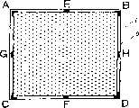
下面,参照图3和图4说明将上述1维的情况下的关系式扩大到2维时的情况。这里,如图3所示,在透明对置电极7的四角形成4个电极A、B、C、D。这些电极A~D通过有源矩阵衬底上的开关电路连接位置检测电路。Next, a case where the relational expression in the case of one dimension described above is extended to two dimensions will be described with reference to FIGS. 3 and 4 . Here, as shown in FIG. 3 , four electrodes A, B, C, and D are formed at the four corners of the
参考图4。如图4所示,对透明对置电极7的四角的电极施加同相、同电位的交流电压,并且因手指等的接触而流过透明对置电极7四角的电流分别为i1、i2、i3和i4。这时,利用与上述计算相同的计算,可得下面的公式。Refer to Figure 4. As shown in FIG. 4 , an AC voltage of the same phase and potential is applied to the four corners of the transparent
X=k1+k2·(i2+i3)/(i1+i2+i3+i4) (式9)X=k1 +k2 ·(i2 +i3 )/(i1 +i2 +i3 +i4 ) (Formula 9)
Y=k1+k2·(i1+i2)/(i1+i2+i3+i4) (式10)Y=k1 +k2 ·(i1 +i2 )/(i1 +i2 +i3 +i4 ) (Formula 10)
这里,X是透明对置电极7上的接触位置的X坐标,Y是透明对置电极7上的接触位置的Y坐标。k1是偏置,k2是倍率,k1和k2是不依赖于人的阻抗的常数。Here, X is the X coordinate of the contact position on the
根据上述式9和式10,可从流过4个电极的电流i1~i4决定接触位置。According to the
上述的例子中,通过在透明对置电极7的四角配置电极,测量流过各电极的电流,检测出具有2维扩展的面上的接触位置,但透明对置电极2的电极数不限于4个。2维位置检测所需的最少电极数为3个,但电极数量增加到5个以上,可提高位置检测的精度。后文详细说明电极数量与位置检测精度的关系。In the above example, by arranging electrodes at the four corners of the
按照上述原理,为了决定接触位置的坐标,需要测量流过透明对置电极7中设置的多个电极的电流值。透明对置电极7还需要对液晶层6施加显示模式中显示所需的规定电压。According to the above principle, in order to determine the coordinates of the contact position, it is necessary to measure the value of the current flowing through the plurality of electrodes provided in the
因此,本实施形态如图5(a)所示,形成TFT阵的有源矩阵衬底4A上与驱动电路一起,配置开关电路。在对置衬底(未示出)上形成透明对置电极7和电极A~D,但有源矩阵衬底4A上设置连接电极A~D的导电构件(图中用A~D表示)。这些导电构件电连接对置衬底上的电极A~D。进行此连接,与已有显示装置中,在对置衬底上的透明对置电极7和有源矩阵衬底4A上的显示电路之间进行的连接相同。Therefore, in this embodiment, as shown in FIG. 5(a), a switching circuit is disposed on an
图5(b)是示出开关电路组成例的电路图。端子50上施加控制开关电路切换的信号。由图中未示出的控制电路产生此控制信号。控制信号为“高”电平时,开关电路内的第1晶体管51为导通状态,晶体管52为非导通状态。这时,电极A~D电连接液晶显示电路的公共电极(COM),接受施加显示所需的电压。Fig. 5(b) is a circuit diagram showing an example of a switch circuit configuration. A signal controlling switching of the switching circuit is applied to
另一方面,控制信号从“高”电平转移到“低”电平时,开关电路内的晶体管51变化到非导通状态,晶体管52为导通状态。结果,电极A、B、C和D分别电连接位置检测电路的端子A’、B’、C’和D’。然后,执行上述电流i1~i4的测量和位置坐标的决定。On the other hand, when the control signal transitions from "high" level to "low" level, the
图5(c)示出透明对置电极7的电位随时间的变化。纵轴表示透明对置电极7的电位,横轴表示时间。由开关电路周期性交互切换位置检测模(周期T1)和显示模式(周期T2)。显示模式中,透明对置电极7的四角全部电短路,给透明对置电极7提供驱动液晶所需的电位(公共电压COM)。另一方面,位置检测模式中,由晶体管和二极管等构成的开关电路使透明对置电极7的四角的电极A~D连接位置检测电路。FIG. 5( c ) shows the change in potential of the
根据常规液晶显示装置结构,最好将位置检测模式的周期T1设定为0.2微秒以上。由于以(T1+T2)的取样周期进行位置检测,周期(T1+T2)如果过长,则在显示面上快速移动手指和笔的接触位置时,产生应随移动连续检测的位置坐标的间隔大的问题。为了避免这种问题,最好将T1+T2设定为17微秒以下。According to the structure of a conventional liquid crystal display device, it is preferable to set the period T1 of the position detection mode to 0.2 microseconds or more. Since the position detection is performed with the sampling period of (T1+T2), if the period (T1+T2) is too long, when the contact position of the finger and the pen is moved rapidly on the display surface, there will be an interval of position coordinates that should be continuously detected along with the movement. Big question. In order to avoid such a problem, it is preferable to set T1+T2 to 17 microseconds or less.
位置检测模式中,将对透明对置电极7时间交流电压的周期设定为例如30~200kHz的范围,电压的振幅设定为例如2~3V的范围。此交流电压上也可加1~2V的直流偏置电压。显示用的公共电压也可不固定为恒定值,例如可使每一显示场极性翻转。In the position detection mode, the period of the AC voltage to the
虽然图5(a)中没有记载,与构成驱动电路和开关电路的晶体管相同,构成位置检测电路的晶体管也最好在有源矩阵衬底4A上形成。这是由于在同一衬底上集成各电路,则不容易产生信号延时造成的信号波形失真,不容易因开关动作而使显示质量下降。Although not shown in FIG. 5(a), like the transistors constituting the driving circuit and the switching circuit, the transistors constituting the position detection circuit are also preferably formed on the
下面。参照图6说明位置检测电路50的组成。under. The configuration of the
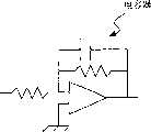
图中所示的位置检测电路50具有4个电流变化检测电路61。电流变化检测电路61在位置检测模式中,测量透明对置电极的电极A~D各自与地之间流通的电流。触摸传感器交流驱动振荡电路65对各电极A~D施加交流电压。因此,由手指等的接触而流过电极A~D的电流具有交流分量。电流变化检测电路61的输出借助模拟信号处理电路62,接受放大和带通滤波。模拟信号处理电路62的示出由检波滤除电路63加以检波后,又输入到消噪声直流电路64。消噪声直流电路64使检波滤除电路63的输出成为直流,并产生具有与流过各电极A~D的电流成正比的值的信号。The
从所述消噪声直流电路64收到上述信号的模拟多路开关选择器66对上述信号进行切换后,将电极A~D的输出按其顺序发送到A/D变换器67。A/D保护区67将数字化的信号(数据)发送到处理装置68。The
处理装置68装在例如具有图1的显示装置的便携型信息终端(PDA)、ATM、售票机或各种计算机内部,执行数据处理。The
检测电路50产生的位置数据不限于上述的例子。检测电路50也可例如用上述数字化的直流电压值求出XY坐标,将其作为位置数据输出。The position data generated by the
以上的位置检测电路随所含各种电流中,不必全部形成在有源矩阵衬底上,但最好在有源矩阵衬底上至少形成包含晶体管51、52的图5(b)的电路和其它TFT阵。The above position detection circuit does not have to be all formed on the active matrix substrate along with the various currents contained, but it is preferable to at least form the circuit of Fig. 5(b) including
本实施形态的带触摸传感器的显示装置中,作为显示装置组成部件的透明对置电极兼作透明导电膜,因而不必另行准备在玻璃等衬底上设置位置检测用的透明导电膜触摸传感器,并且将该传感器叠装在显示屏的图像显示面上。因此,解决以往的触摸传感器衬底部分透射率、反射率等显示质量劣化的问题。In the display device with a touch sensor according to this embodiment, since the transparent counter electrode which is a component of the display device also serves as a transparent conductive film, it is not necessary to separately prepare a transparent conductive film touch sensor for position detection on a substrate such as glass, and the The sensor is stacked on the image display surface of the display screen. Therefore, the problem of degradation in display quality such as partial transmittance and reflectance of the conventional touch sensor substrate is solved.
但是,根据本实施形态,由于位置检测中使用位于2片衬底4、9的内侧区域的电极,手指和笔的接触位置与导电膜之间的距离容易比以往情况下的距离长。此距离变长,则存在位置检测灵敏度降低的倾向。为了避免这种灵敏度降低,最好减小对置衬底9的厚度。对置衬底9的较佳厚度为0.4~0.7mm。However, according to this embodiment, since the electrodes located in the inner regions of the two
本实施形态的显示装置中,设置位置检测用电极的位置不限于透明对置电极的四角。如图7所示,可在电极A和B的中间、电极C和D的中间设置其它电极E、F、G和H。这样设置多个电极时,例如用3个电极A、B和F进行位置检测后,立即用电极C、D和E进行位置检测,从而可提高位置检测的精度。In the display device of this embodiment, the positions where the position detection electrodes are provided are not limited to the four corners of the transparent counter electrode. As shown in FIG. 7, other electrodes E, F, G, and H may be disposed between the electrodes A and B, and between the electrodes C and D. As shown in FIG. When a plurality of electrodes are provided in this way, for example, three electrodes A, B, and F are used for position detection, and electrodes C, D, and E are used for position detection immediately, thereby improving the accuracy of position detection.
又,如图8所示,最好在四角的电极之间设置多个划分电极O1~Onx、P1~Pnx、Q1~Qny以及S1~Sny(nx和ny都是2以上的自然数)。位于电极A、B之间的划分电极O1~Onx包含的电极Oj(其中1≤j≤nx)与位于电极C、D之间的划分电极P1~Pnx包含的电极Pj对应。然后,使j从1到nx依次进行扫描,同时测量分别流过对应的电极Oj和电极Pj的电流。这样,就能高精度决定接触位置的坐标。透明对置电极7的一边形成的电极数能设定为例如4~10个。Also, as shown in FIG. 8, it is preferable to provide a plurality of divided electrodes O1-Onx, P1-Pnx, Q1-Qny, and S1-Sny (both nx and ny are natural numbers greater than 2) between the electrodes at the four corners. The electrodes Oj (where 1≤j≤nx) included in the divided electrodes O1-Onx located between the electrodes A and B correspond to the electrodes Pj included in the divided electrodes P1-Pnx located between the electrodes C and D. Then, j is sequentially scanned from 1 to nx, and the currents flowing through the corresponding electrodes Oj and Pj are measured at the same time. In this way, the coordinates of the contact position can be determined with high precision. The number of electrodes formed on one side of the
根据本实施形态采用的静电容耦合方式,由流过透明对置电极四角的电极的电流大小计算的接触位置与实际接触位置之间有时产生些许偏差。然而,做成扫描多个部位设置的多个电极,并测量流过各电极的电流值,则能实现精度非常高的检测。According to the capacitive coupling method adopted in this embodiment, there may be a slight deviation between the contact position calculated from the magnitude of the current flowing through the electrodes at the four corners of the transparent counter electrode and the actual contact position. However, very high-precision detection can be realized by scanning a plurality of electrodes provided at a plurality of locations and measuring the current value flowing through each electrode.
这样增加电极的数量时,驱动电路、位置检测电路和开关电路相互连接的复杂度按几何级数增加。然而,将开关元件、位置检测电路与驱动电路制入到同一衬底上,则也可不设置多个连接端子,并且用长布线使各电路相互连接。因而,能防止信号延时造成的图像质量变差。When the number of electrodes is increased in this way, the complexity of interconnecting the drive circuit, the position detection circuit and the switch circuit increases geometrically. However, if the switching element, the position detection circuit, and the drive circuit are formed on the same substrate, it is also possible to connect the circuits to each other with long wiring without providing a plurality of connection terminals. Thus, deterioration of image quality due to signal delay can be prevented.
以上说明的实施形态中,由1片透明导电膜构成透明对置电极7。然而,本实施形态的透明对置电极7不限于这样由1片连续的膜组成。例如。如图9所示,也可就透明对置电极7划分成多个部分71~7N。这时,划分部分71~7N分别形成一对电极。采用这样的结构,则图2中能得到1维电阻配置多个的状态。这种情况下,根据流过各划分部分设置的一对电极的电路大小决定有关Y坐标的位置检测。另一方面,X坐标的位置检测,则通过检测哪个划分部分的电路发生变化进行决定。图9的例子中,透明对置电极7的划分部分71~7N的总数(N)越增多,X坐标的位置分辨率越提高。沿X方向的各划分部分的的规模为例如63.5~254微米,较佳N值的范围在例如PDA等的显示点数中为240~480。In the embodiment described above, the
本实施形态用于具有有源矩阵衬底的显示装置,发挥显著的效果,但本实施形态不限于此。本实施形态也能用于例如纯矩阵驱动的显示装置。This embodiment is applied to a display device having an active matrix substrate and exhibits a remarkable effect, but this embodiment is not limited thereto. This embodiment can also be used, for example, in a pure matrix drive display device.
图10以图解方式示出由纯矩阵驱动而动作的显示装置的组成。此显示装置由背面贴有偏振片与相位差片90的第1衬底91和背面贴有偏振片与相位差片96的第2衬底95夹入液晶层。FIG. 10 diagrammatically shows the composition of a display device operated by pure matrix driving. In this display device, a liquid crystal layer is sandwiched between a
第1衬底91的液晶层侧的面上排列往X轴方向延伸的带状扫描电极92。第2衬底95的液晶侧的面上形成滤色镜部94,进而在该部上排列沿Y轴方向延伸的带状扫描电极93。电极92和电极93处于相互交叉的配置关系,这些电极上堆积取向膜(未示出)。Strip-shaped
图10的显示装置中,通过对透明导电膜制作图案形成扫描电极92或数据电极93。位置检测用导电膜兼作扫描电极92或数据电极93。用由与上述开关电路相同的电路切换的驱动电路/位置检测电路控制扫描电极92或数据电极93上施加的电压。In the display device of FIG. 10 ,
本实施形态也能用于液晶显示装置以外的装置,例如有机EL装置。图11(a)和(b)示出有机EL装置的组成例。此显示装置在玻璃衬底100上将透明度机101、液晶正孔输送层102、液晶EL层103和金属电极104依次叠层。透明电极101和金属电极104都排列成带状,但透明电极101和金属电极104配置成交叉。液晶EL层103中产生的光通过玻璃衬底100往下方出射。This embodiment can also be applied to devices other than liquid crystal display devices, such as organic EL devices. 11( a ) and ( b ) show a composition example of an organic EL device. In this display device, a
本实施形态中,在玻璃衬底100的背面侧(显示装置的正面侧)进行手指和笔等的接触。位置检测用透明导电膜划分成带状,即透明电极101也用作位置检测用透明导电膜。In this embodiment, contact with a finger, a pen, or the like is performed on the rear side of the glass substrate 100 (the front side of the display device). The transparent conductive film for position detection is divided into strips, that is, the
用由与上述开关电路相同的电路切换的驱动电路/位置检测电路控制透明电极101上施加的电压。The voltage applied to the
如以上说明那样,根据实施形态1的带触摸传感器的显示装置,能抑制显示屏光透射率的减小,防止显示质量变差。而且,能抑制装置总厚度和重量的增大。As described above, according to the display device with a touch sensor according to
实施形态2
下面,参照图12和图13说明一种本发明的触摸传感器的实施形态。Next, an embodiment of the touch sensor of the present invention will be described with reference to FIGS. 12 and 13 .
实施形态2的触摸传感器37利用静电容耦合方式检测2维(即X方向和Y方向)扩展的操作面内的外部输入点。以下的说明中,说明通过例如用手指和导电笔等接触操作面供给输入点的情况。图12是以图解方式示出触摸传感器37的结构的立体图。The
如图12所示,触摸传感器37具有2片位置检测用透明导电膜(透明电阻膜)(即配置成平行于操作面的第1位置检测用透明导电膜32和配置成与第1位置检测用透明导电膜32对置的第2位置检测用透明导电膜34)、设置在这些位置检测用透明导电膜32、34之间的介质层33和开关电路(未示出)。由绝缘材料形成介质层33。As shown in FIG. 12 , the
根据需要,在第1位置检测用透明导电膜32中设置介质层33的面相反侧的主面设置玻璃31。这样设置玻璃31的情况下,能防止手指和导电笔直接接触触摸传感器37的操作面时,损伤触摸传感器37,又能使反射率减小。图12的触摸传感器37中,玻璃31的主面是操作面,通过例如手指和笔等接触此操作面,对触摸传感器37供给接触点。If necessary, the
如图13所示,第1位置检测用透明导电膜32和第2位置检测用透明导电膜34分别具有检测接触点的坐标一对导电部(导电膜图案)。此导电部作为对位置检测用透明导电膜施加规定电压一对电极起作用。通过例如对金属膜制作图案,形成此导电部。As shown in FIG. 13 , the first transparent
第1位置检测用透明导电膜32上设置的导电部是检测接触点的Y坐标用的Y坐标检测用导电部35。此Y坐标检测用导电部35在第1位置检测用透明导电膜32上的Y方向设置隔开的2个区。另一方面,第2位置检测用透明导电膜34上设置的导电部是检测接触点的X坐标用的X坐标检测用导电部36。此X坐标检测用导电部36在第2位置检测用透明导电膜34上的X方向设置隔开的2个区。The conductive portion provided on the first position detecting transparent
本说明书中的“X方向”和“Y方向”不必是按严格意义的直线规定的方向。触摸传感器和显示屏由柔性材料构成时,操作面可弯曲。即使操作面实际上处于曲面状态,而不是平面的情况下,操作面上的位置也能用2个坐标X、Y表示。The "X direction" and "Y direction" in this specification do not have to be directions defined by a straight line in the strict sense. When the touch sensor and display are made of flexible materials, the operating surface can be bent. Even if the operation surface is actually in a curved state rather than a plane, the position on the operation surface can be represented by two coordinates X, Y.
如图13所示,Y坐标检测用导电部35和X坐标检测用导电部36具有与通常模拟电阻膜方式的触摸传感器的导电部19相同的单纯图案。此导电部35、36的图案与图23所示的已有模拟静电容耦合方式的触摸传感器的导电部19相比,其组成单纯。As shown in FIG. 13 , the Y-coordinate detecting
这样,本实施形态的触摸传感器37具有2片遏制检测用透明导电膜32、34,Y坐标检测用导电部35和X坐标检测用导电部36分别设置在不同的位置检测用透明导电膜32、34上,并且Y坐标检测用导电部35和X坐标检测用导电部36都具有单纯的导电图案,In this way, the
这种Y坐标检测用导电部35和X坐标检测用导电部36连接开关电路(未示出)。利用开关电路的切换,选择性地对Y坐标检测用导电部35和X坐标检测用导电部36的某一方施加交流电压。Y坐标检测用导电部35和X坐标检测用导电部36分别电连接第1位置检测用透明导电膜32和第2位置检测用透明导电膜34,因而利用此开关电路的切换,使第1位置检测用透明导电膜32和第2位置检测用透明导电膜34的某一方电导通,在该位置检测用透明导电膜大致均匀地形成电场。Such a Y-coordinate detecting
下面说明本实施形态的触摸传感器37的位置检测方法。Next, a method for detecting the position of the
例如有选择地对对Y坐标检测用导电部35和X坐标检测用导电部36中的Y坐标检测用导电部35施加电压时,导电笔和手指接触玻璃31的表面,则第1位置检测用透明导电膜32与地(接地面)电容耦合。这时,不对X坐标检测用导电部36施加电压。For example, when a voltage is selectively applied to the Y coordinate detection
该电容是指玻璃31与第1位置检测用导电膜32之间的电容和人与地面之间存在的电容总和的电容。电容耦合的接触部分与第1位置检测用透明导电膜32的Y坐标检测用导电部35之间的电阻值正比于接触部分于Y坐标检测用导电部35之间的距离。因此,Y坐标检测用导电部35流通与接触部分和Y坐标检测用导电部35之间的距离成正比的电流。检测出此电流的大小,就能求出接触点的Y方向的坐标。This capacitance refers to the capacitance of the sum of the capacitance between the
求接触点的X方向的坐标,则利用开关电路的切换有选择地对X坐标检测用导电部36施加电压。这时,不对Y坐标检测用导电部35施加电压。因此,第2位置检测用透明导电膜34与地(接地面)电容耦合。To obtain the X-direction coordinate of the contact point, a voltage is selectively applied to the X-coordinate detection
该电容是指玻璃31与第2位置检测用导电膜34之间的电容和人与地面之间存在的电容的总电容。X坐标检测用导电部36流通与接触部分和X坐标检测用导电部36之间的距离成正比的电流,因而检测出此电流的大小,就能求出接触点的X方向的坐标。以上那样进行后,求出接触点的X方向和Y方向的坐标。This capacitance refers to the total capacitance of the capacitance between the
上述坐标检测方法独立检测接触点的Y坐标和X坐标,因而与同时检测X坐标和Y坐标的已有方法相比,可认为检测费时。然而,能用几毫秒进行一个坐标的检测,因而检测出Y坐标和X坐标需要的时间与人触摸动作相比,足够短,没有问题。The above-mentioned coordinate detection method independently detects the Y coordinate and the X coordinate of the contact point, so compared with the existing method of simultaneously detecting the X coordinate and the Y coordinate, it can be considered that the detection is time-consuming. However, one coordinate can be detected in a few milliseconds, so the time required to detect the Y coordinate and the X coordinate is sufficiently short compared with a human touch action, and there is no problem.
开关电路的连接切换频率为几百kHz。因此,即使操作面上移动接触点时,也能大致实时检测出正在移动的接触点的位置,使该位置大致连续。再者,例如使检测出的位置相比存入存储器,则可将触摸传感器37用作手写输入装置。The connection switching frequency of the switching circuit is several hundred kHz. Therefore, even when the touch point moves on the operation surface, the position of the moving touch point can be detected substantially in real time, and the position can be made substantially continuous. Furthermore, for example, by comparing the detected positions and storing them in a memory, the
本实施形态2中采用的静电容耦合方式的位置检测方法的基本原理与实施形态1中参照图2在上文说明的相同,因而这里省略详细说明。本实施形态2的触摸传感器37中,具有2维扩展的位置检测用透明导电膜32或35发挥与图2的1维电阻相同的功能。具有用的导电部的Y坐标检测用导电部35的各导电部发挥与电极A和电极B相同的功能,而且具有用的导电部的X坐标检测用导电部36的各导电部发挥与电极A和电极B相同的功能。电极A和电极B分别连接电流—电压变换用的电阻。电极A、B连接后文说明的位置检测电路。The basic principle of the position detection method of the electrostatic capacitance coupling method employed in the second embodiment is the same as that described above with reference to FIG. 2 in the first embodiment, and thus detailed description thereof will be omitted here. In the
电极A与地之间和电极B与地之间施加同相、同电位的电压(交流e)。这时,电极A和电极B总处于同电位,因而电极A与电极B之间不流通电流。A voltage (alternating current e) of the same phase and potential is applied between electrode A and ground and between electrode B and ground. At this time, electrode A and electrode B are always at the same potential, so no current flows between electrode A and electrode B.
设接触位置C到电极A的电阻为R1,接触位置C到电极B的电阻为R2,并且R1+R2=R时,可利用实施形态1所示的(式1)~(式8)决定R1/R。Suppose the resistance from contact position C to electrode A is R1, the resistance from contact position C to electrode B is R2, and when R1+R2=R, R1 can be determined by using (Equation 1) to (Equation 8) shown in
本实施形态的触摸传感器37中,第1位置检测用透明导电膜32和第2位置检测用透明导电膜34应用上述原理。在开关电路有选择地对第1位置检测用透明导电膜32施加电压时,根据第1位置检测用透明导电膜32的一对Y坐标检测用导电部35各自流通的电流的测量值,检测出Y坐标的位置(R1/R)。又,在开关电路有选择地对第2位置检测用透明导电膜34施加电压时,根据第2位置检测用透明导电膜34的一对Y坐标检测用导电部36各自流通的电流的测量值,检测出X坐标的位置(R1/R)。结果,能决定接触点的坐标(X、Y坐标)。In the
至此,如上文所说明,本实施形态的触摸传感器37具有2片位置检测用透明导电膜32、34,并且各位置检测用导电膜分别设置Y坐标检测用导电部35和X坐标检测用导电膜36。因此,与只有1片位置检测用透明导电膜,并且在该1片位置检测用透明导电膜设置检测Y轴和X轴方向的位置用的导电部的已有触摸传感器相比,能使坐标检测用导电部的图案单纯。利用这点,能在位置检测用透明导电部上减小形成坐标检测用导电部的区域,因而能扩大可检测接触点的操作面的面积。So far, as described above, the
又,利用开关电路交互切换第2位置检测用透明导电膜32的电导通和第2位置检测用透明导电膜34的电导通,独立检测Y坐标的位置和X坐标的位置。因此,检测一个坐标位置时,另一个坐标位置的检测不受影响,可高精度检测位置坐标。In addition, the electrical conduction of the second position detecting transparent
触摸传感器37中,第1位置检测用透明导电膜32和第2位置检测用透明导电膜34最好由面内具有均匀低电阻的材料形成,例如由铟锡氧化物(ITO)形成。介质层33例如由厚100微米左右的二甲酯(PET)形成。由于PET和IOT具有相同程度的折射率,第1位置检测用透明导电膜32与介质层33的界面或第2位置检测用透明导电膜34与介质层33的界面上不发生反射,能抑制触摸传感器37的透射率下降。又由于介质层33具有上述厚度,能使第1位置检测用透明导电膜32与第2位置检测用透明导电膜34之间可靠绝缘。介质层33的材料除用PET外,还可用具有与PET程度相同的折射率的玻璃和其它透明绝缘物。介质层33的厚度根据使用的材料适当决定。In the
如参照图22所作说明那样,模拟电阻膜方式的触摸传感器需要在2片透明电阻膜12、14之间设置空气层13,由于透明电阻膜12、14与空气层13的反射率不同,存在折射率降低的问题。与此相反,本实施形态的模拟静电容方式的触摸传感器37能在介质层33使用PET那样的具有与ITO程度相同的折射率的材料,因而与模拟电阻膜方式的触摸传感器相比,能抑制透射率下降。As described with reference to FIG. 22 , the touch sensor of the analog resistive film method needs to set an air layer 13 between two transparent
上述位置检测用透明导电膜32、34或介质层33的材料与通常模拟电阻膜方式的触摸错觉光纤使用的材料相同。又,参照图13所作说明那样,触摸传感器37的坐标检测用导电部35、36的图案与通常模拟电阻膜方式的触摸传感器的导电部的图案相同。因此,制造触摸传感器37时,可用现有的模拟电阻膜方式触摸传感器的制造装置和材料,能抑制制造成本升高。The above-mentioned transparent
下面,参照图14说明一例触摸传感器37中设置的位置检测电路50的组成。图14中示出电路61~64各2个,但这些电路的数量不限于图中所示的。例如,如图13所示,第1位置检测用透明导电膜32和第2位置检测用导电膜34分别形成Y坐标检测用导电部35和X坐标检测用导电部36各2个时,由于对1个导电部设置1组电路61~64,位置检测电路50具有4组电路61~64。Next, an example of the configuration of the
图14所示的位置检测电路50具有电流变化检测电路61。电流变化检测电路61测量第1位置检测用透明导电膜32的Y坐标检测用导电部35与地之间流通的电流和第2位置检测用透明导电膜34的X坐标检测用导电部36与地之间流通的电流。利用开关电路69的切换,交互切换Y坐标检测用导电部35与触摸传感器交流驱动振荡电路65的电导通和X坐标检测用导电部36与触摸传感器交流驱动振荡电路65的电导通。于是,触摸传感器交流驱动振荡电路65对Y坐标检测用导电部35和X坐标检测用导电部36中受到选择的一方施加交流电压。因此,由手指等的接触而流过各导电部35、36的电流具有交流分量。The
电流变化检测电路61的示出由模拟信号处理电路62给予放大和带通滤波处理后,进一步输入到消噪声直流化电路64。消噪声直流化电路64使检波滤除电路63的示出成为直流,并产生具有与流过各导电部的电流成正比的值的信号。The output of the current
从消噪声直流化电路64收到上述信号的模拟多路开关选择器66进行上述信号的切换后,将导电部35、36的输出发送到A/D变换器67。A/D变换器67将数字化的信号(数据)发送给处理装置68。The
处理装置68例如装在具有后文参照图16说明的显示装置的便携型信息这点(PDA)、ATM、售票机或各种计算机内,执行数据处理。The
检测电路50产生的位置数据不限于上述的例子。检测电路50也可例如用上述数字化的直流电压值求出XY坐标,将其作为位置数据输出。The position data generated by the
以上说明的实施形态中,第1位置检测用透明导电膜32包括一对导电部的Y坐标检测用导电部35,第2位置检测用透明导电膜34包括一对导电部的X坐标检测用导电部36。然而,本实施形态的位置检测用透明导电膜32、34中手指的导电部35、36的结构不限于此。例如,如图15所示,Y坐标检测用导电部35也可具有在Y方向隔开的3个以上的多个导电部351~35N。同样,X坐标检测用导电部36也可具有在X方向隔开的3个以上的多个导电部361~36N。In the embodiment described above, the first position detection transparent
这时,导电部35、36的图案比图13所示的图案复杂,但由于导电部的数量多,能更正确地检测出接触点的位置。如上文所述,增加导电部的数量时,最好用透明材料形成显示区内配置的导电部。In this case, the pattern of the
如以上所说明,根据实施形态2的触摸传感器,即使将触摸传感器具有的导电图案做得比已有静电容型触摸传感器剧院的导电图案单纯,也能进行高精度的位置检测。As described above, according to the touch sensor of the second embodiment, even if the conductive pattern of the touch sensor is made simpler than that of the conventional capacitive touch sensor, high-precision position detection can be performed.
上述实施形态2的触摸传感器37通常配置在显示屏中使用。图16是具有触摸传感器37的显示装置30的模式图。显示装置30做成在显示屏20的显示面配置触摸传感器37。The
显示屏20包括含矩阵状排列的多个像素电极的有源矩阵衬底22、与该有源矩阵衬底22对置的透明对置衬底24和设置在这些衬底之间的显示媒体层26。透明对置电极24具有设置成与像素电极对置的透明电极。显示屏20可以是例如液晶显示板或有机EL元件。显示屏20是液晶显示板时,显示媒体层26是液晶层,是有机EL元件时,显示媒体层26是有机EL层。The
显示装置30也可将触摸传感器37的第1位置检测用透明导电膜32或第2位置检测用透明导电膜34作为显示屏20的上述透明电极使用。利用这点,能省略1片透明导电膜,因而能抑制透射率下降。下面,说明例如将第2位置检测用透明导电膜34用作显示屏20的透明对置电极的带触摸传感器的显示装置。In the
此带触摸传感器的显示装置具有配置成以显示媒体层为中介与第2位置检测用透明导电膜34对置的有源矩阵衬底22。上述带触摸传感器的显示装置还包括在不对第2位置检测用透明导电膜34施加规定电压(即位置检测用的电压,通常是周期性变化的振荡电压)的周期供给显示用的电压或电流的第1电路、检测第2位置检测用导电膜34中多个部位流通的电流的第2电路和使第1电路中第2电路中的某一方与第2位置检测用透明导电膜34电导通的再一个开关电路。This display device with a touch sensor has an
此带触摸传感器的显示装置使第2位置检测用透明导电膜34也用作透明电极,除对第1位置检测用透明导电膜32和第2位置检测用透明导电膜34中受选择的一方施加位置检测用的规定电压的开关电路外,还包括使第1电路和第2电路中的某一方与第2位置检测用透明导电膜34电导通的再一个开关电路。In this display device with a touch sensor, the second position detection transparent
通过用该再一个开关电路使第1电路和第2电路中的某一方与第2位置检测用透明导电膜34电导通,以时分方式利用第2位置检测用透明导电膜34,进行接触位置的检测和显示电压的施加。因此,触摸传感器的背面方不需要另行设置透明电极,从而可抑制带触摸传感器的显示装置的透射率下降。还能实现带触摸传感器大显示装置的小型化和重量减轻。By making one of the first circuit and the second circuit electrically conduct with the second position detection transparent
例如,如图16所示,在液晶板等显示屏20的正面(观察者方)配置实施形态2的触摸传感器37时,触摸传感器37遭受来自显示屏20的噪声,触摸传感器37的位置检测精度可能降低。例子显示屏20的噪声包含起因于例如显示屏20具有的对置电极上施加的公共电压,而在触摸传感器37具有的位置检测用透明导电膜32、34产生的感应电压。For example, as shown in FIG. 16, when the
为了去除该噪声,实施形态2的带触摸传感器的显示装置从检测接触位置用的检测电路50中检测出的信号减去感应电压对应的信号后,运算接触位置。In order to remove this noise, the display device with a touch sensor according to the second embodiment calculates the touch position after subtracting the signal corresponding to the induced voltage from the signal detected by the
如实施形态2那样,在显示屏20配置静电容耦合方式的触摸传感器37时,在触摸传感器37具有的位置检测以透明导电膜32、34与显示屏20之间配置屏蔽层(未示出),利用此屏蔽层抑制触摸传感器37因来自显示屏20的噪声而受到坏影响。再者,将触摸传感器37的位置检测用透明导电膜32、34配置得充分远离显示屏20,由此也抑制来自显示屏20的噪声的影响。As in
然而,在触摸传感器37与显示屏20之间设置屏蔽层时和使触摸传感器37的位置检测用透明导电膜配置得充分远离显示屏20时,存在视差变大的问题。虽然该屏蔽层存在于显示屏20的显示面至观察者的空间,但有时透射率降低。而且,还存在设置触摸传感器37的显示装置体积大,难以薄型化的问题。However, when a shield layer is provided between the
因此,下面说明一种带触摸传感器的显示装置和位置数据产生方法,可解决上述问题,并且视差小,又能小型化。Therefore, a display device with a touch sensor and a method for generating position data will be described below, which can solve the above-mentioned problems, have small parallax, and can be miniaturized.
实施形态3
首先,参照图17说明一种本发明的带触摸传感器的显示装置的实施形态。First, an embodiment of a display device with a touch sensor according to the present invention will be described with reference to FIG. 17 .
图17以图解方式示出本发明实施形态3的带触摸传感器的显示装置53的组成。FIG. 17 diagrammatically shows the composition of a display device with a touch sensor 53 according to
带触摸传感器的显示装置53具有显示屏49、位置检测用透明导电膜47和检测电路(图17中未示出)。The display device 53 with a touch sensor has a display screen 49 , a transparent conductive film 47 for position detection, and a detection circuit (not shown in FIG. 17 ).
显示屏49至少具有形成媒体层44、配置在显示媒体层44的观察者方而且用于驱动显示媒体层44的透明对置电极45和配置在透明对置电极45的观察者方的绝缘层(介质层)46。位置检测用透明导电膜47配置成以该显示屏49具有的绝缘层46为中介与透明对置电极45对置。检测电路检测位置检测用透明导电膜47中多个部位流通的电流变化。The display screen 49 has at least a transparent opposite electrode 45 that forms the media layer 44, is disposed on the observer's side of the display media layer 44 and is used to drive the display media layer 44, and an insulating layer ( medium layer) 46. The transparent conductive film 47 for position detection is disposed so as to face the transparent counter electrode 45 via the insulating layer 46 included in the display screen 49 . The detection circuit detects changes in electric current flowing through a plurality of locations in the transparent conductive film 47 for position detection.
带触摸传感器的显示装置53,其主要特征为:通过在透明对置电极45施加周期性变化的振荡电压,使位置检测用透明导电膜47产生感应电压,在位置检测用透明导电膜47上形成电场,并且根据由位置检测用透明导电膜47形成接触点而产生的电流变化,产生接触点的位置数据。The display device 53 with a touch sensor is mainly characterized in that: by applying a periodically changing oscillating voltage to the transparent counter electrode 45, the transparent conductive film 47 for position detection generates an induced voltage, and the transparent conductive film 47 for position detection is formed on the transparent conductive film 47. The electric field, and the position data of the contact point are generated according to the change of current generated when the contact point is formed by the transparent conductive film 47 for position detection.
一般地、带触摸传感器的显示装置中,因透明对置电极施加公共电压而在位置检测用透明导电膜产生的感应电压,一般认为对触摸传感器是噪声。因此,为了抑制位置检测用透明导电膜产生感应电压,将位置检测用透明导电膜与透明对置电极的间隔取得足够大。或者,在位置检测用透明导电膜与透明对置电极之间配置屏蔽层。或者,如上文所述,从检测接触位置用的检测电路中检测出的信号减去上述感应电压对应的信号后,运算接触位置。Generally, in a display device with a touch sensor, an induced voltage generated in a position detecting transparent conductive film by applying a common voltage to a transparent counter electrode is considered to be noise to the touch sensor. Therefore, in order to suppress the induced voltage from being generated in the position-detecting transparent conductive film, the distance between the position-detecting transparent conductive film and the transparent counter electrode is made sufficiently large. Alternatively, a shield layer is disposed between the position detecting transparent conductive film and the transparent counter electrode. Alternatively, as described above, the contact position is calculated by subtracting the signal corresponding to the induced voltage from the signal detected by the detection circuit for detecting the contact position.
与此相反,本实施形态3的带触摸传感器的显示装置53积极利用一般认为是噪声的感应电压,产生对位置检测用透明导电膜47的接触点的位置数据。因此,不必将位置检测用透明导电膜47与透明对置电极45的间隔取大。也不必在显示屏49与位置检测用透明导电膜47之间设置屏蔽层。因而,能提供可薄型化且视差小的带触摸传感器的显示装置。On the contrary, the display device 53 with a touch sensor according to the third embodiment actively utilizes the induced voltage which is generally considered to be noise, and generates position data of the contact point to the position detecting transparent conductive film 47 . Therefore, it is not necessary to increase the distance between the position detecting transparent conductive film 47 and the transparent counter electrode 45 . It is also unnecessary to provide a shield layer between the display screen 49 and the transparent conductive film 47 for position detection. Therefore, it is possible to provide a display device with a touch sensor that can be thinned and has a small parallax.
为了检测接触位置,不是用专门对位置检测用透明导电膜47施加的电压,而是利用对透明对置电极45施加的周期性变化的振荡电压所产生的感应电压。因此,不需要复杂的电路,不会增加耗电。作为这种振荡电压,可利用为驱动显示媒体层而显示屏本来就有的电压。而且,位置检测用透明导电膜47不必另行施加交流电压。In order to detect the contact position, an induced voltage generated by a periodically changing oscillating voltage applied to the transparent counter electrode 45 is used instead of a voltage applied exclusively to the position detecting transparent conductive film 47 . Therefore, there is no need for complicated circuits and no increase in power consumption. As this oscillating voltage, the voltage inherent in the display panel for driving the display medium layer can be used. Furthermore, it is not necessary to separately apply an AC voltage to the transparent conductive film 47 for position detection.
下面,参照图17说明带触摸传感器的显示装置53的具体例。以下的说明中,示出显示屏49用液晶板时的例子。Next, a specific example of the display device 53 with a touch sensor will be described with reference to FIG. 17 . In the following description, an example in which a liquid crystal panel is used for the display screen 49 will be shown.
显示屏49用液晶板时,例如,如图17所示,显示屏49除具有绝缘层46、透明对置电极45和含液晶材料的显示媒体层44外,还包括配置成隔着显示媒体层44与透明对置电极45对置的有源矩阵衬底48和第1偏振片41。有源矩阵衬底48在玻璃等透明材料形成的衬底42的主面形成TFT阵43,并且矩阵状排列像素电极(图中未示出)。When the display screen 49 uses a liquid crystal panel, for example, as shown in Figure 17, the display screen 49, except having an insulating layer 46, a transparent opposite electrode 45 and a display medium layer 44 containing a liquid crystal material, also includes a display medium layer configured to separate the display medium layer. 44 and the active matrix substrate 48 and the first polarizer 41 opposite to the transparent counter electrode 45 . Active matrix substrate 48 forms TFT array 43 on the main surface of substrate 42 made of a transparent material such as glass, and pixel electrodes (not shown) are arranged in a matrix.
绝缘层46例如是玻璃衬底或塑料衬底等的对置衬底,而且根据需要,也可具有滤色镜和第2偏振片。上述滤色镜和第2偏振片可配置在位置检测用透明导电膜47的观察者方。绝缘层46的较佳厚度只要能使位置检测用透明导电膜47产生足够大的感应电压的程度即可。The insulating layer 46 is, for example, a counter substrate such as a glass substrate or a plastic substrate, and may have a color filter and a second polarizer as necessary. The above-mentioned color filter and the second polarizing plate may be arranged on the observer's side of the transparent conductive film 47 for position detection. The preferred thickness of the insulating layer 46 may be such that a sufficiently large induced voltage can be generated in the position detecting transparent conductive film 47 .
具体的绝缘层46的较佳厚度取决于绝缘层包含的材料的介电常数。后文将说明,为了在位置检测用透明导电膜47产生足够大的感应电压,位置检测用导电膜47与透明对置电极45和它们之间的绝缘层形成的电容的值最好是200pF以上。因此,例如3.7型液晶板的绝缘层采用玻璃衬底时,玻璃衬底的厚度最好设定下0mm以上、1.1mm以下的范围。现状下,采用0.4mm以上的玻璃衬底。液晶板的尺寸大于3.7型时,即使玻璃衬底的厚度电压1.1mm,也能使电容的值为200pF以上。The preferred thickness of a particular insulating layer 46 depends on the dielectric constant of the material the insulating layer comprises. As will be described later, in order to generate a sufficiently large induced voltage in the position detection transparent conductive film 47, the value of the capacitance formed by the position detection conductive film 47, the transparent counter electrode 45 and the insulating layer between them is preferably 200 pF or more. . Therefore, for example, when a glass substrate is used as the insulating layer of a 3.7-type liquid crystal panel, the thickness of the glass substrate is preferably set in the range of not less than 0 mm and not more than 1.1 mm. Currently, glass substrates of 0.4 mm or more are used. When the size of the liquid crystal panel is larger than the 3.7 type, even if the thickness voltage of the glass substrate is 1.1mm, the capacitance value can be made to be 200pF or more.
可在显示装置53的最靠近观察者方的表面形成保护层。A protective layer may be formed on the surface of the display device 53 closest to the viewer.
液晶板一般接受交流驱动,其原因是液晶层上施加直流电压时,液晶层的寿命短等。因此,作为公共电压,对透明对置电极45施加正、负极性周期性翻转的电压。The liquid crystal panel is generally driven by AC. The reason is that when a DC voltage is applied to the liquid crystal layer, the life of the liquid crystal layer is short. Therefore, a voltage whose positive and negative polarities are periodically reversed is applied to the transparent counter electrode 45 as a common voltage.
图18(a)是示出一例显示屏49的透明对置电极45上施加的公共电压随时间的变化的图。纵轴表示透明对置电极45的电位,横轴表示时间。这里示出行翻转驱动时的例子,但本发明不限于此。FIG. 18( a ) is a graph showing an example of the change with time of the common voltage applied to the transparent counter electrode 45 of the display panel 49 . The vertical axis represents the potential of the transparent counter electrode 45, and the horizontal axis represents time. Here, an example of row inversion driving is shown, but the present invention is not limited thereto.
如图18(a)所示,公共电压每一水平扫描周期翻转正、负极性,而且正极性的电压绝对值等于负极性的电压绝对值。带触摸传感器的显示装置53中,该公共电压为使位置检测用透明导电膜47产生感应电压用的振荡电压。As shown in FIG. 18( a ), the positive and negative polarities of the common voltage are reversed every horizontal scanning period, and the absolute value of the voltage of the positive polarity is equal to the absolute value of the voltage of the negative polarity. In the display device 53 with a touch sensor, this common voltage is an oscillating voltage for generating an induced voltage in the transparent conductive film 47 for position detection.
图18(b)示出透明对置电极45上施加图18(a)所示的公共电压时位置检测用导电膜47产生的感应电压随时间的变化。纵轴表示位置检测用透明导电膜47的电位,横轴表示时间。此感应电压与图18(a)所示的透明对置电极45的电压变化同步,是每一水平扫描周期有最大值或最小值的脉冲波。以例如约40kHz的周期出现上述最大值或最小值。图18(b)所示的感应电压充分大于因供给有源矩阵衬底48的显示信号而产生的感应电压。FIG. 18( b ) shows the change with time of the induced voltage generated by the position detection conductive film 47 when the common voltage shown in FIG. 18( a ) is applied to the transparent counter electrode 45 . The vertical axis represents the potential of the transparent conductive film 47 for position detection, and the horizontal axis represents time. This induced voltage is synchronized with the voltage change of the transparent counter electrode 45 shown in FIG. 18( a ), and is a pulse wave having a maximum value or a minimum value in each horizontal scanning period. The above-mentioned maximum or minimum values occur at a cycle of, for example, about 40 kHz. The induced voltage shown in FIG. 18( b ) is sufficiently larger than the induced voltage generated by the display signal supplied to the active matrix substrate 48 .
通过位置检测用透明导电膜47产生图18(a)所示感应电压,在位置检测用透明导电膜47内大致均匀地形成梯度小的电场。The induced voltage shown in FIG. 18( a ) is generated by the transparent conductive film 47 for position detection, and an electric field with a small gradient is formed substantially uniformly in the transparent conductive film 47 for position detection.
位置检测用导电膜47例如在四角形成位置检测用的电极。带触摸传感器的显示装置53在其最靠近观察者方的表面设置保护层时,通过用笔和手指等接触该保护膜,在位置检测用透明导电膜47上形成接触点。位置检测用透明导电膜47上形成接触点,则位置检测用透明导电膜47与地(接地面)电容耦合。此电容是指例如保护层与位置检测用透明导电膜47之间的电容和人与地之间存在的电容的总电容。In the conductive film 47 for position detection, for example, electrodes for position detection are formed at four corners. When the display device 53 with a touch sensor is provided with a protective layer on its surface closest to the viewer, contact points are formed on the transparent conductive film 47 for position detection by touching the protective film with a pen or finger. When a contact point is formed on the transparent conductive film 47 for position detection, the transparent conductive film 47 for position detection is capacitively coupled to the ground (ground plane). This capacitance refers to, for example, the total capacitance of the capacitance between the protective layer and the transparent conductive film 47 for position detection and the capacitance existing between a person and the ground.
电容耦合的接触部分与位置检测用透明导电膜47的四角的电极之间的电阻值正比于接触部分于各电极之间的距离。因此,通过位置检测用透明导电膜47四角的电极,流通接触部分和各电极之间的距离成正比的电流。检测出这些电流的大小,就能求出接触部分的位置坐标。The resistance value between the capacitively coupled contact portion and the electrodes at the four corners of the position detecting transparent conductive film 47 is proportional to the distance between the contact portion and each electrode. Therefore, through the electrodes at the four corners of the transparent conductive film 47 for position detection, a current proportional to the distance between the contact portion and each electrode flows. By detecting the magnitude of these currents, the position coordinates of the contact parts can be obtained.
例如实施形态2的带触摸传感器的显示装置或已有的一般带触摸传感器的显示装置中,通过用振荡器(例如图14的振荡电路65)对位置检测用透明导电膜时间规定的交流电压,在位置检测用透明导电膜内对置均匀地形成梯度小的电场,以进行接触位置的检测。与此相反,本实施形态3带触摸传感器的显示装置53如上文所述,利用透明对置电极45上施加的振荡电压在位置检测用透明导电膜47产生的感应电压,使位置检测用透明导电膜47内大致均匀地形成梯度小的电场。进而,根据位置检测用透明导电膜47上产生的电场的变化所产生的电流变化,产生接触点的位置数据。For example, in the display device with a touch sensor of
即,带触摸传感器的显示装置53使用通常得不到有效利用的感应电压,产生接触点的位置数据。因此,不需要一般对位置检测用透明导电膜47施加交流电压所需的振荡电路,与一般带触摸传感器的显示装置相比,可省电。通常认为上述的感应电压是噪声,因而为了抑制该感应电压的发生,在透明对置电极45与位置检测用透明导电膜47之间设置屏蔽层,并且/或者将透明对置电极45与位置检测用透明导电膜47之间的距离取大,但带触摸传感器的显示装置53不必这样。That is, the display device 53 with a touch sensor generates the position data of the touch point using the induced voltage which is not normally utilized effectively. Therefore, an oscillation circuit generally required for applying an AC voltage to the transparent conductive film 47 for position detection is unnecessary, and power can be saved compared to a general display device with a touch sensor. It is generally considered that the above-mentioned induced voltage is noise, so in order to suppress the generation of this induced voltage, a shielding layer is provided between the transparent opposite electrode 45 and the transparent conductive film 47 for position detection, and/or the transparent opposite electrode 45 and the position detection The distance between the transparent conductive films 47 is large, but it is not necessary for the display device 53 with a touch sensor.
带触摸传感器的显示装置中,在透明对置电极45与位置检测用透明导电膜47之间将玻璃衬底和空气层作为绝缘层(介质层),形成虚拟电容。如上文所述,本实施形态中,由于将感应电压用于位置检测,在例如显示屏是3.7型(显示面的对角线长度为3.7英寸)的情况下,为了足够大的感应电压,上述电容的值最好是200pF。In the display device with a touch sensor, a glass substrate and an air layer are used as an insulating layer (dielectric layer) between the transparent counter electrode 45 and the transparent conductive film 47 for position detection to form a dummy capacitance. As mentioned above, in this embodiment, since the induced voltage is used for position detection, for example, in the case of a 3.7-type display screen (the diagonal length of the display surface is 3.7 inches), in order to have a sufficiently large induced voltage, the above-mentioned The value of the capacitor is preferably 200pF.
例如,设液晶板10为3.7型,在透明对置电极45与位置检测用透明导电膜47之间配置厚度为0.7mm的玻璃衬底,并且在玻璃衬底与位置检测用透明导电膜47之间设置厚度0.1mm的空气层的间隙的情况下,透明对置电极45与位置检测用透明导电膜47之间的距离为0.8mm,上述电容的值为192pF。For example, if the liquid crystal panel 10 is a 3.7 type, a glass substrate with a thickness of 0.7 mm is arranged between the transparent counter electrode 45 and the transparent conductive film 47 for position detection, and between the glass substrate and the transparent conductive film 47 for position detection When a gap of an air layer with a thickness of 0.1 mm is provided between them, the distance between the transparent counter electrode 45 and the transparent conductive film 47 for position detection is 0.8 mm, and the value of the above capacitance is 192 pF.
使透明对置电极45与位置检测用透明导电膜47之间的距离为0.8mm,并且对透明对置电极45施加例如振幅为4.9V的图18(a)所示的电压时,实际测量到位置检测用透明导电膜47产生振幅为0.65V的图18(b)所示的感应电压。此感应电压的大小足以进行本实施形态的位置检测。When the distance between the transparent counter electrode 45 and the transparent conductive film 47 for position detection is 0.8mm, and when the voltage shown in FIG. The transparent conductive film 47 for position detection generates an induced voltage shown in FIG. 18( b ) with an amplitude of 0.65V. The magnitude of this induced voltage is sufficient for the position detection of this embodiment.
与此相反,一般带触摸传感器的显示装置中,为了一种上述感应电压的发生,将透明对置电极与位置检测用透明导电膜之间的距离取大,使上述电容的值减小。On the contrary, in a general display device with a touch sensor, the distance between the transparent counter electrode and the transparent conductive film for position detection is made large to reduce the value of the above-mentioned capacitance in order to generate the above-mentioned induced voltage.
例如,设液晶板为3.7型,在透明对置电极与位置检测用透明导电膜之间配置厚度为0.7mm的玻璃衬底,并且在玻璃衬底与位置检测用透明导电膜之间设置厚度0.5mm的空气层的间隙的情况下,透明对置电极与位置检测用透明导电膜之间的距离为1.2mm,上述电容的值为62.5pF。已有的电阻膜方式带触摸传感器的显示装置的电阻膜与透明对置电极之间需要长度和此透明对置电极与位置检测用透明导电膜之间的距离相同的距离。For example, assuming that the liquid crystal panel is a 3.7 type, a glass substrate with a thickness of 0.7 mm is arranged between the transparent counter electrode and the transparent conductive film for position detection, and a thickness of 0.5 mm is arranged between the glass substrate and the transparent conductive film for position detection. In the case of an air layer gap of mm, the distance between the transparent counter electrode and the transparent conductive film for position detection is 1.2 mm, and the value of the above capacitance is 62.5 pF. In a conventional resistive film type display device with a touch sensor, the distance between the resistive film and the transparent counter electrode needs to be the same as the distance between the transparent counter electrode and the transparent conductive film for position detection.
如以上所说明,带触摸传感器的显示装置53中,能将透明对置电极45与位置检测用透明导电膜47之间的距离做成1mm以下,因而能比一般带触摸传感器的显示装置贴近透明对置电极45和位置检测用透明导电膜47,可减小视差。As described above, in the display device 53 with a touch sensor, the distance between the transparent counter electrode 45 and the transparent conductive film 47 for position detection can be set to 1 mm or less, so that it can be more transparent than a display device with a general touch sensor. The counter electrode 45 and the transparent conductive film 47 for position detection can reduce parallax.
实施形态2的带触摸传感器的显示装置30(图16)中,如上文所述,为了对位置检测用透明导电膜32、34的坐标检测用导电部35、36施加电压,使用交流驱动振荡电路65(图14)。此外,例如在位置检测用透明导电膜32、34与透明对置衬底24具有的电极(例如对置电极)之间设置屏蔽层(未示出),并且/或者将在位置检测用透明导电膜32、34与透明对置衬底24具有的对置电极的间隔取大。将此显示装置30用于实施形态3时,可将显示屏20中透明对置衬底24的对置电极上施加的周期性变化的振荡电压所产生的感应电压用于位置检测。In the
下面,参照图16较具体地说明对显示装置30应用实施形态3的情况。以下的说明中,示出对置电极上施加的振荡电压使第2位置检测用透明导电膜34产生感应电压时的例子。Next, a case where
实施形态3中应用显示装置30时,显示屏20至少具有显示媒体层26和显示媒体层26配置在观察者方的透明对置衬底24。透明对置衬底24具有驱动显示媒体层26用的电极和该电极配置在观察者方的绝缘层(例如玻璃衬底)。第2位置检测与透明导电膜34配置成以绝缘层未中介与上述电极对置。通过对上述电极施加周期性变化的振荡电压,使第2位置检测用透明导电膜34产生感应电压,在该第2位置检测用透明导电膜34形成电场。根据通过第1位置检测用透明导电膜32和第2位置检测用透明导电膜34上形成接触点而产生的电流变化,产生接触点的位置数据。When the
根据上述显示装置,由于有效利用被认为是噪声的感应电压,不必在电极与位置检测用透明电极34之间设置屏蔽层,或将电极与第2位置检测用透明导电膜34的间隔取大。为了检测接触位置,不是用专门对位置检测用透明导电膜34施加的电压,而是利用对电极施加的周期性变化的振荡电压所产生的感应电压,能省略对位置检测用透明导电膜34施加振荡电压用的交流驱动振荡电路。因此,显示装置30用于实施形态3时,使视差减小,并能使显示装置小型化,还可降低耗电。According to the above display device, since the induced voltage considered to be noise is effectively used, it is not necessary to provide a shield layer between the electrode and the
上述说明中,示出用透明对置电极45上施加的公共电压产生感应电压时的例子,但为产生感应电压而在透明对置电极45施加的电压不限于此。In the above description, an example was shown in which the induced voltage is generated by the common voltage applied to the transparent opposing electrode 45 , but the voltage applied to the transparent opposing electrode 45 to generate the induced voltage is not limited to this.
例如,也可与公共电压分开,对透明对置电极45施加在位置检测用透明导电膜47产生感应电压用的振荡电压。图18(c)示出此具体例。其中,纵轴表示透明对置电极45的电位,横轴表示时间。图18(c)所示的透明对置电极45的电位的一个周期包含周期T1和周期T2。For example, an oscillating voltage for generating an induced voltage in the position detecting transparent conductive film 47 may be applied to the transparent counter electrode 45 separately from the common voltage. Fig. 18(c) shows this specific example. Here, the vertical axis represents the potential of the transparent counter electrode 45 and the horizontal axis represents time. One period of the potential of the transparent counter electrode 45 shown in FIG. 18(c) includes a period T1 and a period T2.
在图18(c)的情况下,切换将透明对置电极45用作显示用的公共电极的周期(显示模式)和用作使位置检测用透明导电膜47产生感应电压用的电极的周期(位置检测模式)周期T1和周期T2分别对应于位置检测模式和显示模式。In the case of FIG. 18( c), the cycle (display mode) in which the transparent counter electrode 45 is used as a common electrode for display and the cycle (display mode) used as an electrode for generating an induced voltage in the transparent conductive film 47 for position detection is switched ( position detection mode) period T1 and period T2 correspond to the position detection mode and the display mode, respectively.
位置检测用透明导电膜47四角的电极分别用晶体管和二极管等组成的开关电路连接后文说明的检测电路。例如通过用此开关电路交互切换周期T1和周期T2。即,此开关电路使对透明对置电极45提供驱动显示媒体层44用的电压或电流的显示电路和减小位置检测用的检测电路中的某一方与透明对置电极45电导通。The electrodes at the four corners of the transparent conductive film 47 for position detection are respectively connected to a detection circuit described later by a switch circuit composed of a transistor and a diode. For example, the period T1 and the period T2 are alternately switched by using this switching circuit. That is, the switch circuit electrically connects the transparent counter electrode 45 to the transparent counter electrode 45 either of a display circuit for supplying a voltage or current for driving the display medium layer 44 and a detection circuit for detecting the reduced position.
周期T1的期间,位置检测用透明导电膜47四角的电极分别连接检测电路,周期T2的期间,位置检测用透明导电膜47四角的电极不连接检测电路。During the period T1, the electrodes at the four corners of the position detecting transparent conductive film 47 are respectively connected to the detection circuit, and during the period T2, the electrodes at the four corners of the position detecting transparent conductive film 47 are not connected to the detection circuit.
首先,周期T1的位置检测模式中,对透明对置电极45时间具有规定振幅的振荡电压,使位置检测用透明导电膜47产生具有规定振幅的感应电压。此周期T1期间,位置检测用透明导电膜47四角的电极分别连接后文说明的检测电路,因而由该检测电路产生接触点的位置数据。First, in the position detection mode of the period T1, an oscillating voltage with a predetermined amplitude is applied to the transparent counter electrode 45 for a period of time, and an induced voltage with a predetermined amplitude is generated in the position detection transparent conductive film 47 . During this period T1, the electrodes at the four corners of the position detection transparent conductive film 47 are respectively connected to a detection circuit described later, so that the detection circuit generates position data of the contact point.
另一方面,周期T2的显示模式中,施加规定大小的公共电压,并且公共电压如以上所述那样产生振荡时,位置检测用透明导电膜47上产生感应电压,但周期T2期间位置检测用透明导电膜47四角的电极不连接检测电路,因而感应电压不影响接触位置的检测精度。再者,如图18(c)所示,周期T2期间在透明对置电极45施加恒定电压时,位置检测用透明导电膜47不产生感应电压,因而可省略上述开关电路。On the other hand, in the display mode of the period T2, when a common voltage of a predetermined magnitude is applied and the common voltage oscillates as described above, an induced voltage is generated on the position detecting transparent conductive film 47, but the position detecting transparent conductive film 47 is transparent during the period T2. The electrodes at the four corners of the conductive film 47 are not connected to the detection circuit, so the induced voltage does not affect the detection accuracy of the contact position. Furthermore, as shown in FIG. 18(c), when a constant voltage is applied to the transparent counter electrode 45 during the period T2, the position detection transparent conductive film 47 does not generate an induced voltage, so the above-mentioned switching circuit can be omitted.
本实施形态3中采用的静电容耦合方式位置检测方法的基本原理与实施形态1中用图2、4说明的相同,因而数量详细说明。再者,例如图4中,从位置检测用透明导电膜四角的电极施加同相、同电位的交流电压,但实施形态3不是利用振荡电路对位置检测用导电膜施加上述交流电压,而是用透明对置电极45上施加的振荡电压产生感应电压。The basic principle of the capacitive coupling method position detection method used in the third embodiment is the same as that described in the first embodiment with reference to Figs. Furthermore, for example, in FIG. 4 , an AC voltage of the same phase and potential is applied from the electrodes at the four corners of the transparent conductive film for position detection. The oscillating voltage applied to the counter electrode 45 generates an induced voltage.
如实施形态1所说明,可从流过位置检测用导电膜47四角的电流i1、i2、i3和i4(图4)的测量值求出对位置检测用导电膜47的接触位置。As described in
以上的说明中,示出显示屏49是液晶板,尤其该液晶板是有源矩阵型液晶板时的例子,但本实施形态使用的显示屏49不限于此。只要显示屏具有的透明对置电极施加周期性变化的振荡电压,任何显示屏都可用。这里,透明对置电极上施加的振荡电压最好是用于驱动显示媒体层的电压。为了使位置检测用透明导电膜产生感应电压,需要振荡电压,该振荡电压只要是用于驱动显示媒体层的公共电压,除公共电压外,不必对透明对置电极另行施加产生感应电压用的电压。因此,与通常的显示装置相比,能抑制电源电路结构复杂,又能抑制耗电增大。In the above description, the display screen 49 is a liquid crystal panel, particularly an example in which the liquid crystal panel is an active matrix type liquid crystal panel, but the display screen 49 used in this embodiment is not limited to this. Any display screen can be used as long as a periodically changing oscillating voltage is applied to the transparent counter electrode that the display screen has. Here, the oscillating voltage applied to the transparent counter electrode is preferably a voltage for driving the display medium layer. In order to generate an induced voltage on the transparent conductive film for position detection, an oscillating voltage is required. As long as the oscillating voltage is a common voltage for driving the display medium layer, it is not necessary to apply a voltage for generating an induced voltage to the transparent counter electrode separately from the common voltage. . Therefore, it is possible to suppress an increase in power consumption while suppressing the complexity of the configuration of the power supply circuit compared to a typical display device.
使位置检测用透明导电膜47产生感应电压的电极不限于上述的透明对置电极45。但是,对位置检测用透明导电膜47施加相互不同的振荡电压的多个电极对置,则这些电极与位置检测用透明导电膜47之间的电场不均匀,有时位置检测精度会下降。因此,为了能在产生感应电压用的电极与位置检测用透明导电膜47之间产生具有的电场,至少在检测接触位置的位置检测用透明导电膜47的整个区域设置成该位置检测用透明导电膜47与产生感应电压用的电极相互对置为佳。The electrode for generating an induced voltage in the transparent conductive film 47 for position detection is not limited to the above-mentioned transparent counter electrode 45 . However, if a plurality of electrodes applying different oscillating voltages to the transparent conductive film for position detection 47 face each other, the electric field between these electrodes and the transparent conductive film for position detection 47 will become uneven, and the position detection accuracy may decrease. Therefore, in order to generate an electric field between the electrode for generating the induced voltage and the transparent conductive film 47 for position detection, at least the entire area of the transparent conductive film 47 for position detection that detects the contact position is provided with a transparent conductive film for position detection. It is preferable that the membrane 47 and the electrode for generating the induced voltage are opposed to each other.
下面说明带触摸传感器的显示装置53具有的检测电路。检测电路检测位置检测用透明导电膜47中多个部位流通的电流变化,并根据检测出的电流变化,产生对位置检测用透明导电膜47的接触点的位置数据。Next, a detection circuit included in the display device with a touch sensor 53 will be described. The detection circuit detects changes in the current flowing through multiple locations in the position-detecting transparent conductive film 47 , and generates position data of the contact point to the position-detecting transparent conductive film 47 based on the detected current changes.
图19是示出一例检测电路50的框图。图19作为例子示出的检测电路50具有4个电流变化检测电路61,这些电路61分别连接位置检测用透明导电膜47四角的电极。位置检测用透明导电膜47上设置的电极数量及其配置不限于此。FIG. 19 is a block diagram showing an example of the
电流变化检测电路61测量位置检测用透明导电膜47四角的电极各自与地之间流通的电流。位置检测用透明导电膜47上施加上述感应电压,因而由手指等的接触而流过各电极的电流具有交流分量。The current
电流变化检测电路61的输出,由模拟信号处理电路62给予放大和导通滤波处理。模拟信号处理电路62的输出则由检波过虑电路63A加以检波。The output of the current
检波滤除电路63A为了滤除接收信号包含的各种噪声,进行滤波。一般认为由透明对置电极上施加电压而在位置检测用透明导电膜产生的感应电压(例如图18(b))也是噪声。因此,检波滤除电路滤除的噪声中也包含与上述感应电压对应的信号。The
与此相反,本实施形态的检测电路由于积极利用上述感应电压,以检测接触点位置,检波滤除电路63A不去除上述感应电压对应的信号。因此,本实施形态的检波滤除电路63A不包含滤除上述感应电压对应的信号用的电路。On the contrary, since the detection circuit of this embodiment actively utilizes the above-mentioned induced voltage to detect the position of the contact point, the detection and
检波滤除电路63A的示出输入到消噪声直流电路64。该电路64使检波滤除电路64A的输出成为直流,并产生具有与流过各电极的电路成正比的值的信号。消噪声直流电路64还将检测出的电流值变换成电压值,并加以放大后,通过模拟电路开关选择器66送到A/D变换器67。The output of the
例如实施形态2的消噪声直流电路中从检波滤除电路收到的信号(电压值)已去除感应电压对应的信号。因此,从检波滤除电路收到的信号不叠加图18(b)所示的感应电压,具有对时间连续变化的波形。于是,实施形态2的消噪声直流电路通过模拟多路开关选择器将具有上述连续变化波形的电压值连续输入到A/D变换器。For example, the signal (voltage value) received from the detection and filtering circuit in the noise elimination DC circuit of
与此相反,本实施形态中,从检波滤除电路63A收到的信号(电压值)叠加例如图18(b)所示的感应电压,具有图21(a)所示的非连续波形。因此,例如与实施形态2同样通过模拟多路开关选择器将消噪声直流电路检测出的信号连续输入到A/D变换器时,由于不输入接触位置时,信号也变动,不能正确检测出接触位置。图21(a)示出一例消噪声直流电路64从检波滤除电路63A收到的信号(电压值)随时间的变化。纵轴表示电位,横轴表示时间。On the contrary, in this embodiment, the signal (voltage value) received from the
因此,本实施形态的检测电路50如图20所示,在噪声直流电路64包含的放大电路中设置电容器。例如在感应电压是以周期40kHz具有最大值或最小值的脉冲波的情况下,最好设置静电容为几百nF的电容器。通过设置电容器,将图21(b)所示不存在感应电压时检测的电流值与存在感应电压时检测的电流值取平均后,给A/D变换器67提供直流电压。根据位置检测用透明导电膜47未形成接触点时得到的直流电压值与形成接触点时得到的直流电压值之差,求出接触点的位置。Therefore, in the
从消噪声直流电路64接收上述信号的模拟多路开关选择器66将4个电极的输出发送到A/D变换器67。A/D变换器67产生数字化的位置信号(位置数据),并发送到处理装置68。这里所说的位置数据是指将上述式9和式10的i1、i2、i3和i4变换成直流电压值后,进一步将这些值数字化所得的数据。处理装置68用这些值,根据式9和式10求坐标X、Y,判断形成接触点的操作者输入的命令,以进行规定的数据处理等。处理装置68装在具有例如图17的显示装置的便携型信息终端(PDA)、ATM、售票机或各种计算机内部,执行数据处理。The
检测电路50产生的位置数据不限于上述的例子。检测电路50也可例如用上述数字化的直流电压值求XY坐标,并将其作为位置数据输出。The position data generated by the
如以上所说明,利用实施形态3能提供薄型、视差小且不需要复杂电路结构的带触摸传感器的显示装置和位置数据检测方法。As described above, according to the third embodiment, it is possible to provide a display device with a touch sensor and a position data detection method that are thin, have small parallax, and do not require a complicated circuit configuration.
工业上的实用性Industrial Applicability
根据本发明,可提供重量轻、适合小型化且不会导致显示特性变差的触摸传感器、带触摸传感器的显示装置和位置数据检测方法。而且能提供具有结构比以往简单的电路的触摸传感器和带触摸传感器的显示装置。According to the present invention, it is possible to provide a touch sensor, a display device with a touch sensor, and a position data detection method that are lightweight, suitable for miniaturization, and do not cause deterioration of display characteristics. Furthermore, it is possible to provide a touch sensor and a display device with a touch sensor having a simpler circuit structure than conventional ones.
Claims (16)
Applications Claiming Priority (6)
| Application Number | Priority Date | Filing Date | Title |
|---|---|---|---|
| JP252076/2001 | 2001-08-22 | ||
| JP2001252076AJP2003066417A (en) | 2001-08-22 | 2001-08-22 | Touch sensor integrated display |
| JP2001371246AJP2003173238A (en) | 2001-12-05 | 2001-12-05 | Touch sensor and display device with touch sensor |
| JP371246/2001 | 2001-12-05 | ||
| JP171739/2002 | 2002-06-12 | ||
| JP2002171739AJP2004021327A (en) | 2002-06-12 | 2002-06-12 | Display device with touch sensor and position data generation method |
Related Child Applications (1)
| Application Number | Title | Priority Date | Filing Date |
|---|---|---|---|
| CNB2006100044895ADivisionCN100429609C (en) | 2001-08-22 | 2002-07-18 | Touch sensor, display with touch sensor, and method for generating position data |
Publications (2)
| Publication Number | Publication Date |
|---|---|
| CN1520544A CN1520544A (en) | 2004-08-11 |
| CN1275131Ctrue CN1275131C (en) | 2006-09-13 |
Family
ID=27347368
Family Applications (1)
| Application Number | Title | Priority Date | Filing Date |
|---|---|---|---|
| CNB028128435AExpired - Fee RelatedCN1275131C (en) | 2001-08-22 | 2002-07-18 | Touch sensor, display device with touch sensor and position data generation method |
Country Status (6)
| Country | Link |
|---|---|
| US (2) | US8031180B2 (en) |
| EP (3) | EP2267584A1 (en) |
| KR (1) | KR100642183B1 (en) |
| CN (1) | CN1275131C (en) |
| TW (1) | TWI225219B (en) |
| WO (1) | WO2003019346A1 (en) |
Families Citing this family (261)
| Publication number | Priority date | Publication date | Assignee | Title |
|---|---|---|---|---|
| GB9722766D0 (en) | 1997-10-28 | 1997-12-24 | British Telecomm | Portable computers |
| US7663607B2 (en) | 2004-05-06 | 2010-02-16 | Apple Inc. | Multipoint touchscreen |
| CN1275131C (en)* | 2001-08-22 | 2006-09-13 | 夏普株式会社 | Touch sensor, display device with touch sensor and position data generation method |
| US7254775B2 (en)* | 2001-10-03 | 2007-08-07 | 3M Innovative Properties Company | Touch panel system and method for distinguishing multiple touch inputs |
| US7952570B2 (en) | 2002-06-08 | 2011-05-31 | Power2B, Inc. | Computer navigation |
| DE602004027705D1 (en) | 2003-02-10 | 2010-07-29 | N trig ltd | TOUCH DETECTION FOR A DIGITIZER |
| GB0313808D0 (en)* | 2003-06-14 | 2003-07-23 | Binstead Ronald P | Improvements in touch technology |
| GB0317715D0 (en)* | 2003-07-29 | 2003-09-03 | Koninkl Philips Electronics Nv | Display and input device |
| US7307624B2 (en)* | 2003-12-30 | 2007-12-11 | 3M Innovative Properties Company | Touch sensor with linearized response |
| JP4060313B2 (en)* | 2004-01-28 | 2008-03-12 | シャープ株式会社 | Display device |
| EP1735770A4 (en) | 2004-02-27 | 2012-04-25 | N trig ltd | Noise reduction in digitizer system |
| FR2866799B1 (en)* | 2004-03-01 | 2006-04-21 | Sopro | CAMERA FOR MEDICAL AND IN PARTICULAR DENTAL USE |
| US7196696B2 (en)* | 2004-03-19 | 2007-03-27 | Tsung-Ying Li | Position touch screen panel and method of arranging a resistive sensing circuit thereof |
| GB2424269A (en) | 2004-04-01 | 2006-09-20 | Robert Michael Lipman | Control apparatus |
| US7492358B2 (en)* | 2004-06-15 | 2009-02-17 | International Business Machines Corporation | Resistive scanning grid touch panel |
| WO2006030745A1 (en)* | 2004-09-17 | 2006-03-23 | Sharp Kabushiki Kaisha | Display, viewing angle controller, and electronic apparatus |
| US8184145B2 (en)* | 2004-10-04 | 2012-05-22 | Sharp Kabushiki Kaisha | Display device and electronic apparatus |
| US8274481B2 (en)* | 2004-10-22 | 2012-09-25 | Sharp Kabushiki Kaisha | Display device with touch sensor, and drive method for the device |
| US8576217B2 (en) | 2011-05-20 | 2013-11-05 | Ignis Innovation Inc. | System and methods for extraction of threshold and mobility parameters in AMOLED displays |
| US10013907B2 (en) | 2004-12-15 | 2018-07-03 | Ignis Innovation Inc. | Method and system for programming, calibrating and/or compensating, and driving an LED display |
| US9799246B2 (en) | 2011-05-20 | 2017-10-24 | Ignis Innovation Inc. | System and methods for extraction of threshold and mobility parameters in AMOLED displays |
| US8610675B2 (en) | 2007-03-14 | 2013-12-17 | Power2B, Inc. | Interactive devices |
| US10452207B2 (en) | 2005-05-18 | 2019-10-22 | Power2B, Inc. | Displays and information input devices |
| JP5355080B2 (en) | 2005-06-08 | 2013-11-27 | イグニス・イノベイション・インコーポレーテッド | Method and system for driving a light emitting device display |
| US7920127B2 (en)* | 2005-07-29 | 2011-04-05 | Alps Electric Co., Ltd. | Capacitive coordinate detection device |
| US20070034423A1 (en)* | 2005-08-12 | 2007-02-15 | Rebeschi Thomas J | Touch screen having reduced susceptibility to radio frequency interference |
| US8284169B2 (en)* | 2005-09-01 | 2012-10-09 | Sharp Kabushiki Kaisha | Display device |
| JP2009508205A (en) | 2005-09-08 | 2009-02-26 | パワー2ビー,インコーポレイティド | Display and information input device |
| US8350823B2 (en)* | 2005-09-14 | 2013-01-08 | Sharp Kabushiki Kaisha | Coordinate position detecting device |
| US20070085838A1 (en)* | 2005-10-17 | 2007-04-19 | Ricks Theodore K | Method for making a display with integrated touchscreen |
| KR100640822B1 (en) | 2005-11-22 | 2006-11-02 | 엘지전자 주식회사 | Glass touch key input device |
| KR101230309B1 (en) | 2006-01-27 | 2013-02-06 | 삼성디스플레이 주식회사 | Display device and processing apparatus of sensing signal |
| JP5268262B2 (en)* | 2006-02-24 | 2013-08-21 | キヤノン株式会社 | Electroluminescence display device |
| US8013943B2 (en)* | 2006-03-08 | 2011-09-06 | Sharp Kabushiki Kaisha | Display device |
| US8040142B1 (en) | 2006-03-31 | 2011-10-18 | Cypress Semiconductor Corporation | Touch detection techniques for capacitive touch sense systems |
| TW200746022A (en) | 2006-04-19 | 2007-12-16 | Ignis Innovation Inc | Stable driving scheme for active matrix displays |
| US8004497B2 (en)* | 2006-05-18 | 2011-08-23 | Cypress Semiconductor Corporation | Two-pin buttons |
| CN104965621B (en) | 2006-06-09 | 2018-06-12 | 苹果公司 | Touch screen LCD and its operating method |
| US8259078B2 (en) | 2006-06-09 | 2012-09-04 | Apple Inc. | Touch screen liquid crystal display |
| CN101467120B (en)* | 2006-06-09 | 2012-12-12 | 苹果公司 | Touch screen liquid crystal display |
| GB2451210B8 (en)* | 2006-06-09 | 2011-03-02 | Apple Inc | Touch screen liquid crystal display. |
| CN102981678B (en)* | 2006-06-09 | 2015-07-22 | 苹果公司 | Touch screen liquid crystal display |
| JP2008041051A (en)* | 2006-08-10 | 2008-02-21 | Alps Electric Co Ltd | Coordinate input device |
| CA2556961A1 (en)* | 2006-08-15 | 2008-02-15 | Ignis Innovation Inc. | Oled compensation technique based on oled capacitance |
| JP4567028B2 (en)* | 2006-09-26 | 2010-10-20 | エルジー ディスプレイ カンパニー リミテッド | Liquid crystal display device having multi-touch sensing function and driving method thereof |
| US8547114B2 (en) | 2006-11-14 | 2013-10-01 | Cypress Semiconductor Corporation | Capacitance to code converter with sigma-delta modulator |
| US8159462B1 (en)* | 2006-11-15 | 2012-04-17 | Cypress Semiconductor Corporation | Reference voltage offset for capacitive touch-sensor measurement |
| JP4916852B2 (en)* | 2006-11-29 | 2012-04-18 | 株式会社 日立ディスプレイズ | LCD with touch panel |
| EP1936479A1 (en)* | 2006-12-22 | 2008-06-25 | Research In Motion Limited | Integrated Liquid Crystal Display and Touchscreen for an Electronic Device |
| US20080150901A1 (en)* | 2006-12-22 | 2008-06-26 | Robert Lowles | Integrated Liquid Crystal Display And Touchscreen For An Electronic Device |
| US8493330B2 (en) | 2007-01-03 | 2013-07-23 | Apple Inc. | Individual channel phase delay scheme |
| US9710095B2 (en) | 2007-01-05 | 2017-07-18 | Apple Inc. | Touch screen stack-ups |
| JP5051690B2 (en)* | 2007-01-30 | 2012-10-17 | 株式会社ジャパンディスプレイウェスト | Display device with input function |
| US8058937B2 (en) | 2007-01-30 | 2011-11-15 | Cypress Semiconductor Corporation | Setting a discharge rate and a charge rate of a relaxation oscillator circuit |
| KR101359921B1 (en)* | 2007-03-02 | 2014-02-07 | 삼성디스플레이 주식회사 | Display device |
| JP4356757B2 (en) | 2007-03-13 | 2009-11-04 | セイコーエプソン株式会社 | Liquid crystal device, electronic device and position specifying method |
| DE102007020873A1 (en)* | 2007-04-26 | 2008-10-30 | Ident Technology Ag | Sensor device, and methods for generating signals indicative of the position or position change of limbs |
| JP5060845B2 (en)* | 2007-06-27 | 2012-10-31 | 株式会社ジャパンディスプレイイースト | Screen input type image display device |
| US9500686B1 (en) | 2007-06-29 | 2016-11-22 | Cypress Semiconductor Corporation | Capacitance measurement system and methods |
| US8570053B1 (en) | 2007-07-03 | 2013-10-29 | Cypress Semiconductor Corporation | Capacitive field sensor with sigma-delta modulator |
| US8169238B1 (en) | 2007-07-03 | 2012-05-01 | Cypress Semiconductor Corporation | Capacitance to frequency converter |
| KR101530188B1 (en)* | 2007-07-05 | 2015-06-19 | (주)멜파스 | Touchscreen apparatus |
| KR101530189B1 (en)* | 2007-07-19 | 2015-06-22 | (주)멜파스 | Touchscreen apparatus having multiple bar-type transparent electrodes |
| JP5380723B2 (en)* | 2007-08-07 | 2014-01-08 | Nltテクノロジー株式会社 | Surface display device and electronic device |
| JP4791427B2 (en)* | 2007-09-19 | 2011-10-12 | 三菱自動車工業株式会社 | EL light-emitting touch switch |
| EP2053495A3 (en)* | 2007-10-23 | 2011-04-27 | Tsinghua University | Touch panel, method for making the same, and display device adopting the same |
| JP2009122969A (en)* | 2007-11-15 | 2009-06-04 | Hitachi Displays Ltd | Screen input type image display device |
| US9215301B2 (en) | 2007-12-13 | 2015-12-15 | Creator Technology B.V. | Electronic device with a flexible panel and method for manufacturing a flexible panel |
| TWI374379B (en) | 2007-12-24 | 2012-10-11 | Wintek Corp | Transparent capacitive touch panel and manufacturing method thereof |
| US8389883B2 (en)* | 2007-12-27 | 2013-03-05 | Byd Co., Ltd. | Key-press structure and a method for making the same |
| US8525798B2 (en) | 2008-01-28 | 2013-09-03 | Cypress Semiconductor Corporation | Touch sensing |
| KR101237640B1 (en)* | 2008-01-29 | 2013-02-27 | (주)멜파스 | Touchscreen apparatus having structure for preventing forming of parasitic capacitance |
| US20090189875A1 (en)* | 2008-01-29 | 2009-07-30 | Research In Motion Limited | Electronic device and touch screen display |
| EP2085861A1 (en)* | 2008-01-29 | 2009-08-05 | Research In Motion Limited | Electronic device and touch screen display |
| KR101354274B1 (en)* | 2008-02-21 | 2014-01-24 | 주식회사 옵솔 | Liquid Crystal Display Device integrated touch panel |
| US8358142B2 (en) | 2008-02-27 | 2013-01-22 | Cypress Semiconductor Corporation | Methods and circuits for measuring mutual and self capacitance |
| US8319505B1 (en) | 2008-10-24 | 2012-11-27 | Cypress Semiconductor Corporation | Methods and circuits for measuring mutual and self capacitance |
| US9104273B1 (en) | 2008-02-29 | 2015-08-11 | Cypress Semiconductor Corporation | Multi-touch sensing method |
| JP4816668B2 (en)* | 2008-03-28 | 2011-11-16 | ソニー株式会社 | Display device with touch sensor |
| JP5224242B2 (en)* | 2008-04-09 | 2013-07-03 | Nltテクノロジー株式会社 | Display device, liquid crystal display device, electronic apparatus, and manufacturing method for display device |
| KR100955339B1 (en)* | 2008-04-22 | 2010-04-29 | 주식회사 애트랩 | Display panels and display devices capable of detecting touch and access and methods of detecting touch and access using the panel |
| TWI397850B (en) | 2008-05-14 | 2013-06-01 | Ind Tech Res Inst | Sensing apparatus and scanning actuation method thereof |
| CN102084326A (en)* | 2008-05-14 | 2011-06-01 | 3M创新有限公司 | Systems and methods for assessing locations of multiple touch inputs |
| JP5279898B2 (en)* | 2008-05-23 | 2013-09-04 | エーティーラブ・インコーポレーテッド | Contact sensor device and operation mode switching method of the device |
| JP5106268B2 (en)* | 2008-06-24 | 2012-12-26 | 富士通コンポーネント株式会社 | Touch panel |
| US8508495B2 (en) | 2008-07-03 | 2013-08-13 | Apple Inc. | Display with dual-function capacitive elements |
| JP2010015412A (en)* | 2008-07-04 | 2010-01-21 | Hitachi Displays Ltd | Display device equipped with touch panel |
| JPWO2010004867A1 (en)* | 2008-07-08 | 2012-01-05 | セイコーインスツル株式会社 | Electrostatic detection device, information device, and electrostatic detection method |
| JP4966924B2 (en)* | 2008-07-16 | 2012-07-04 | 日東電工株式会社 | Transparent conductive film, transparent conductive laminate and touch panel, and method for producing transparent conductive film |
| JP5372630B2 (en)* | 2008-07-17 | 2013-12-18 | Nltテクノロジー株式会社 | Display device and driving method of display device |
| FR2934921B1 (en)* | 2008-08-05 | 2010-09-24 | Stantum | MULTICONTACT TOUCH SENSOR WITH VARIABLE SIZE AND IMPEDANCE SPACING MEANS |
| JP2010061494A (en)* | 2008-09-05 | 2010-03-18 | Sony Corp | Information processor, information announcing method, and computer program |
| TWI378376B (en) | 2008-09-23 | 2012-12-01 | Au Optronics Corp | Multi-touch positioning method for capacitive touch panel |
| US8321174B1 (en) | 2008-09-26 | 2012-11-27 | Cypress Semiconductor Corporation | System and method to measure capacitance of capacitive sensor array |
| US9137353B2 (en)* | 2008-09-29 | 2015-09-15 | Kyocera Corporation | Electronic device and display method employed in electronic device |
| US20100097344A1 (en)* | 2008-10-16 | 2010-04-22 | Tpo Displays Corp. | Electronic apparatus with a capacitive touch sensor |
| US20100108409A1 (en)* | 2008-11-06 | 2010-05-06 | Jun Tanaka | Capacitive coupling type touch panel |
| US8144295B2 (en) | 2008-11-18 | 2012-03-27 | Apple Inc. | Common bus design for a TFT-LCD display |
| US8749496B2 (en) | 2008-12-05 | 2014-06-10 | Apple Inc. | Integrated touch panel for a TFT display |
| US11143896B2 (en)* | 2008-12-11 | 2021-10-12 | Au Optronics Corp. | Touch device and touch display panel |
| TWI376537B (en)* | 2008-12-11 | 2012-11-11 | Au Optronics Corp | Structure of touch device and touch panel |
| CN101751170B (en)* | 2008-12-12 | 2011-12-28 | 胜华科技股份有限公司 | Touch panel and circuit thereof |
| TWI381043B (en)* | 2008-12-12 | 2013-01-01 | Ghitron Technology Co Ltd | Ion dielectric type touch sensor and device thereof |
| TWI401588B (en)* | 2008-12-26 | 2013-07-11 | Higgstec Inc | Touch panel with parallel electrode pattern |
| US8217913B2 (en) | 2009-02-02 | 2012-07-10 | Apple Inc. | Integrated touch screen |
| US7995041B2 (en) | 2009-02-02 | 2011-08-09 | Apple Inc. | Integrated touch screen |
| JP5484891B2 (en)* | 2009-03-04 | 2014-05-07 | 株式会社ジャパンディスプレイ | Display device |
| US8643624B2 (en)* | 2009-03-18 | 2014-02-04 | Synaptics Incorporated | Capacitive sensing using a segmented common voltage electrode of a display |
| JP5366051B2 (en)* | 2009-04-20 | 2013-12-11 | 株式会社ジャパンディスプレイ | Information input device, display device |
| US20100271328A1 (en)* | 2009-04-22 | 2010-10-28 | Shinji Sekiguchi | Input device and display device having the same |
| JP2010287215A (en)* | 2009-05-11 | 2010-12-24 | Ricoh Co Ltd | Information input apparatus, image forming apparatus, input control method, and recording medium recording input control program |
| JP5178631B2 (en) | 2009-05-26 | 2013-04-10 | 株式会社ジャパンディスプレイウェスト | Touch sensor, display device, and electronic device |
| US9384698B2 (en) | 2009-11-30 | 2016-07-05 | Ignis Innovation Inc. | System and methods for aging compensation in AMOLED displays |
| US9311859B2 (en) | 2009-11-30 | 2016-04-12 | Ignis Innovation Inc. | Resetting cycle for aging compensation in AMOLED displays |
| US10319307B2 (en) | 2009-06-16 | 2019-06-11 | Ignis Innovation Inc. | Display system with compensation techniques and/or shared level resources |
| US8253706B2 (en) | 2009-06-26 | 2012-08-28 | Atmel Corporation | Apparatus using a differential analog-to-digital converter |
| WO2011001933A1 (en) | 2009-07-01 | 2011-01-06 | シャープ株式会社 | Display device |
| JP5086394B2 (en)* | 2009-07-07 | 2012-11-28 | ローム株式会社 | Touch panel control circuit, control method, touch panel input device using them, and electronic device |
| CN101943967B (en)* | 2009-07-08 | 2012-08-15 | 群康科技(深圳)有限公司 | Method for positioning touch screen |
| US9323398B2 (en)* | 2009-07-10 | 2016-04-26 | Apple Inc. | Touch and hover sensing |
| TWI395126B (en)* | 2009-07-20 | 2013-05-01 | Mstar Semiconductor Inc | Sensing apparatus and method applied to touch screen |
| US8441465B2 (en)* | 2009-08-17 | 2013-05-14 | Nokia Corporation | Apparatus comprising an optically transparent sheet and related methods |
| KR101077032B1 (en)* | 2009-08-19 | 2011-10-26 | 주식회사 실리콘웍스 | Timing adjusting method for touch screen liquid crystal display device |
| TW201132990A (en)* | 2009-08-24 | 2011-10-01 | Cambrios Technologies Corp | Contact resistance measurement for resistance linearity in nanostructure thin films |
| US8390582B2 (en)* | 2009-08-25 | 2013-03-05 | Apple Inc. | Integrated touch screen |
| JP5552772B2 (en)* | 2009-08-26 | 2014-07-16 | ソニー株式会社 | Information processing apparatus, information processing method, and computer program |
| EP2290510B1 (en)* | 2009-08-27 | 2018-07-04 | BlackBerry Limited | Touch-sensitive display with capacitive and resistive touch sensors and method of control |
| TWI463382B (en)* | 2009-09-14 | 2014-12-01 | Raydium Semiconductor Corp | Touch sensing apparatus and touch sensing method |
| TWI407355B (en)* | 2009-11-19 | 2013-09-01 | Elan Microelectronics Corp | Detection and Correction of Capacitive Touchpad |
| KR101642149B1 (en)* | 2010-01-05 | 2016-07-25 | 삼성전자주식회사 | Method and apparatus for controlling haptic feedback in portable terminal having touch-screen |
| US20140313111A1 (en) | 2010-02-04 | 2014-10-23 | Ignis Innovation Inc. | System and methods for extracting correlation curves for an organic light emitting device |
| US9881532B2 (en) | 2010-02-04 | 2018-01-30 | Ignis Innovation Inc. | System and method for extracting correlation curves for an organic light emitting device |
| US10089921B2 (en) | 2010-02-04 | 2018-10-02 | Ignis Innovation Inc. | System and methods for extracting correlation curves for an organic light emitting device |
| CA2692097A1 (en) | 2010-02-04 | 2011-08-04 | Ignis Innovation Inc. | Extracting correlation curves for light emitting device |
| CN102884496B (en)* | 2010-02-26 | 2017-06-30 | 辛纳普蒂克斯公司 | Modify demodulation to avoid interference |
| KR101073320B1 (en)* | 2010-04-01 | 2011-10-12 | 삼성모바일디스플레이주식회사 | Touch screen panel and its manufacturing method |
| US9898121B2 (en) | 2010-04-30 | 2018-02-20 | Synaptics Incorporated | Integrated capacitive sensing and displaying |
| JP5528926B2 (en)* | 2010-07-09 | 2014-06-25 | 株式会社ジャパンディスプレイ | Detection device and display device |
| KR20120017587A (en)* | 2010-08-19 | 2012-02-29 | 삼성모바일디스플레이주식회사 | Touch Screen Panel Integrated LCD |
| US9851829B2 (en) | 2010-08-27 | 2017-12-26 | Apple Inc. | Signal processing for touch and hover sensing display device |
| JP5458443B2 (en) | 2010-09-14 | 2014-04-02 | 株式会社ジャパンディスプレイ | Display device with touch detection function and electronic device |
| KR101398238B1 (en)* | 2010-10-01 | 2014-05-22 | 엘지디스플레이 주식회사 | Display device having touch screen panel |
| JP2012088915A (en)* | 2010-10-19 | 2012-05-10 | Hosiden Corp | Contact type coordinate input device, touch panel having contact type coordinate input device, and electronic device |
| KR101230146B1 (en)* | 2010-10-29 | 2013-02-05 | 삼성디스플레이 주식회사 | Liquid Crystal Display integrated Touch Screen Panel and Driving Method thereof |
| CN103250350A (en) | 2010-11-30 | 2013-08-14 | 瑟克公司 | Linear projected single-layer capacitance sensor |
| TW201227454A (en)* | 2010-12-31 | 2012-07-01 | Hong-Da Liu | An active array having the touchable sensing matrix unit and a display having the active array |
| US9069421B2 (en) | 2010-12-16 | 2015-06-30 | Hung-Ta LIU | Touch sensor and touch display apparatus and driving method thereof |
| US8941607B2 (en)* | 2010-12-16 | 2015-01-27 | Hung-Ta LIU | MEMS display with touch control function |
| EP2469327A3 (en)* | 2010-12-22 | 2012-11-28 | Chimei InnoLux Corporation | Touch panel |
| US8804056B2 (en) | 2010-12-22 | 2014-08-12 | Apple Inc. | Integrated touch screens |
| KR20120072220A (en)* | 2010-12-23 | 2012-07-03 | 한국전자통신연구원 | Touch-sensitive input device and electromagnetic-wave transcieving device using its |
| JP5797908B2 (en)* | 2011-02-08 | 2015-10-21 | ローム株式会社 | Touch panel control circuit, touch panel input device using the same, and electronic device |
| DE102012003281B4 (en)* | 2011-02-24 | 2014-02-13 | Tokai Rubber Industries, Ltd. | touch switch |
| JP5637894B2 (en)* | 2011-02-24 | 2014-12-10 | 住友理工株式会社 | Touch switch |
| CN102692743A (en)* | 2011-03-25 | 2012-09-26 | 京东方科技集团股份有限公司 | Electronic equipment, thin-film transistor liquid crystal flat-panel display and manufacturing method thereof |
| US9530349B2 (en) | 2011-05-20 | 2016-12-27 | Ignis Innovations Inc. | Charged-based compensation and parameter extraction in AMOLED displays |
| TWI456467B (en)* | 2011-05-20 | 2014-10-11 | Au Optronics Corp | Operating method of capacitive touch panel and touch control barrier-type 3d display device |
| US9466240B2 (en) | 2011-05-26 | 2016-10-11 | Ignis Innovation Inc. | Adaptive feedback system for compensating for aging pixel areas with enhanced estimation speed |
| US9773439B2 (en) | 2011-05-27 | 2017-09-26 | Ignis Innovation Inc. | Systems and methods for aging compensation in AMOLED displays |
| TWI454979B (en)* | 2011-05-30 | 2014-10-01 | Elan Microelectronics Corp | Method of distinguishing a plurality of objects on a touch panel and computer readable medium |
| KR101978666B1 (en) | 2011-06-10 | 2019-05-15 | 미래나노텍(주) | Substrate for Touch Screen Sensor, Touch Screen Sensor and Touch Screen Panel |
| US8766657B2 (en)* | 2011-06-17 | 2014-07-01 | Microsoft Corporation | RF proximity sensor |
| JP5757800B2 (en)* | 2011-06-24 | 2015-08-05 | 富士通コンポーネント株式会社 | Touch panel |
| CN102929455A (en)* | 2011-08-11 | 2013-02-13 | 微创高科有限公司 | Touch control capacitance detection circuit and method applied to liquid crystal display module |
| CN103765354B (en)* | 2011-08-30 | 2017-03-15 | Nlt科技股份有限公司 | Electronic equipment, electrostatic capacitance sensor and touch panel |
| US8907921B2 (en) | 2011-08-30 | 2014-12-09 | Synaptics Incorporated | Interference sensing within a display device with an integrated sensing device |
| JP5925896B2 (en) | 2011-09-07 | 2016-05-25 | シナプティクス インコーポレイテッド | Capacitive detection during hidden update time |
| US9046976B2 (en)* | 2011-09-28 | 2015-06-02 | Hung-Ta LIU | Method for transmitting and detecting touch sensing signals and touch device using the same |
| US9529479B2 (en)* | 2011-10-14 | 2016-12-27 | Hung-Ta LIU | Touch sensing method, module, and display |
| TWI596515B (en)* | 2011-10-14 | 2017-08-21 | 劉鴻達 | Touch sensing method with interlacing driving scheme, touch sensing module and display |
| US9075488B2 (en) | 2011-11-03 | 2015-07-07 | Synaptics Incorporated | Virtual geometries for integrated display and sensing devices |
| US9176621B2 (en) | 2011-11-18 | 2015-11-03 | Synaptics Incorporated | Flexible timing and multiplexing for a display device comprising an integrated capacitive sensing device |
| US9324268B2 (en) | 2013-03-15 | 2016-04-26 | Ignis Innovation Inc. | Amoled displays with multiple readout circuits |
| US10089924B2 (en) | 2011-11-29 | 2018-10-02 | Ignis Innovation Inc. | Structural and low-frequency non-uniformity compensation |
| US8994673B2 (en)* | 2011-12-09 | 2015-03-31 | Lg Display Co., Ltd. | Display device with integrated touch screen having electrical connections provided in inactive regions of display panel |
| JP6022164B2 (en)* | 2012-01-24 | 2016-11-09 | 株式会社ジャパンディスプレイ | Liquid crystal display |
| US8780028B2 (en) | 2012-01-27 | 2014-07-15 | Blackberry Limited | Electronic device with capacitive touch-sensitive display |
| US9262020B2 (en) | 2012-01-27 | 2016-02-16 | Blackberry Limited | Electronic device with capacitive touch-sensitive display |
| US8970547B2 (en) | 2012-02-01 | 2015-03-03 | Synaptics Incorporated | Noise-adapting touch sensing window |
| US8937632B2 (en) | 2012-02-03 | 2015-01-20 | Ignis Innovation Inc. | Driving system for active-matrix displays |
| KR101364075B1 (en)* | 2012-03-14 | 2014-02-20 | 엘지디스플레이 주식회사 | Display device with integrated touch screen |
| TW201342171A (en)* | 2012-04-12 | 2013-10-16 | Rich Ip Technology Inc | Electronic paper touch control device |
| TWI436411B (en)* | 2012-04-27 | 2014-05-01 | Liu Hung Ta | Touch device |
| US9201547B2 (en) | 2012-04-30 | 2015-12-01 | Apple Inc. | Wide dynamic range capacitive sensing |
| US9086768B2 (en) | 2012-04-30 | 2015-07-21 | Apple Inc. | Mitigation of parasitic capacitance |
| TWI607258B (en)* | 2012-05-14 | 2017-12-01 | 友達光電股份有限公司 | Touch display and method for driving a touch display |
| US8922544B2 (en) | 2012-05-23 | 2014-12-30 | Ignis Innovation Inc. | Display systems with compensation for line propagation delay |
| US9395583B2 (en) | 2012-06-06 | 2016-07-19 | Apple Inc. | Column spacer design for a display incorporating a third metal layer |
| JP6055206B2 (en)* | 2012-06-08 | 2016-12-27 | 株式会社ジャパンディスプレイ | Liquid crystal display |
| TW201351225A (en)* | 2012-06-11 | 2013-12-16 | Giantplus Technology Co Ltd | A circuit structure for an in-cell touch and display panel |
| US9280231B2 (en) | 2012-06-20 | 2016-03-08 | Synaptics Incorporated | Disabling display lines during input sensing periods |
| US9920207B2 (en) | 2012-06-22 | 2018-03-20 | C3Nano Inc. | Metal nanostructured networks and transparent conductive material |
| US10029916B2 (en) | 2012-06-22 | 2018-07-24 | C3Nano Inc. | Metal nanowire networks and transparent conductive material |
| JP6037146B2 (en)* | 2012-06-29 | 2016-11-30 | パナソニックIpマネジメント株式会社 | Touch panel device with tactile presentation function |
| US10073568B2 (en) | 2012-08-15 | 2018-09-11 | Synaptics Incorporated | System and method for interference avoidance for a display device comprising an integrated sensing device |
| US8970546B2 (en) | 2012-08-31 | 2015-03-03 | Synaptics Incorporated | Method and apparatus for improved input sensing using a display processor reference signal |
| CN102830848B (en) | 2012-09-07 | 2015-12-02 | 京东方科技集团股份有限公司 | Touch liquid crystal display device, display panels, array base palte and color membrane substrates |
| US10073550B2 (en) | 2012-09-20 | 2018-09-11 | Synaptics Incorporated | Concurrent input sensing and display updating |
| KR101305924B1 (en)* | 2012-10-23 | 2013-09-09 | 엘지디스플레이 주식회사 | Display device and driving method thereof |
| US11340731B2 (en)* | 2012-11-27 | 2022-05-24 | Microsoft Technology Licensing, Llc | Detection with a capacitive based digitizer sensor |
| TW201423710A (en)* | 2012-12-12 | 2014-06-16 | Rich Ip Technology Inc | Driving circuit using display structure to provide touch function, and touch display |
| CN103293785B (en)* | 2012-12-24 | 2016-05-18 | 上海天马微电子有限公司 | TN (twisted nematic) type liquid crystal display device and touch control method thereof |
| US9336723B2 (en) | 2013-02-13 | 2016-05-10 | Apple Inc. | In-cell touch for LED |
| US10020807B2 (en) | 2013-02-26 | 2018-07-10 | C3Nano Inc. | Fused metal nanostructured networks, fusing solutions with reducing agents and methods for forming metal networks |
| US8970577B2 (en) | 2013-03-13 | 2015-03-03 | Synaptics Incorporated | Reducing display artifacts after non-display update periods |
| EP3043338A1 (en) | 2013-03-14 | 2016-07-13 | Ignis Innovation Inc. | Re-interpolation with edge detection for extracting an aging pattern for amoled displays |
| TWI490746B (en)* | 2013-03-29 | 2015-07-01 | Chunghwa Picture Tubes Ltd | Control system applied to touch and capable of switching two-dimensional/three-dimensional mode |
| CN103246396B (en) | 2013-04-18 | 2016-03-30 | 北京京东方光电科技有限公司 | Touch display circuit structure and driving method, array base palte and display device |
| US9715291B2 (en) | 2013-06-18 | 2017-07-25 | Synaptics Incorporated | Pre-charging a gate electrode before resuming display updating |
| US9442615B2 (en) | 2013-10-02 | 2016-09-13 | Synaptics Incorporated | Frequency shifting for simultaneous active matrix display update and in-cell capacitive touch |
| US11274223B2 (en) | 2013-11-22 | 2022-03-15 | C3 Nano, Inc. | Transparent conductive coatings based on metal nanowires and polymer binders, solution processing thereof, and patterning approaches |
| US9933879B2 (en) | 2013-11-25 | 2018-04-03 | Apple Inc. | Reconfigurable circuit topology for both self-capacitance and mutual capacitance sensing |
| CN105814523B (en) | 2013-12-02 | 2019-05-14 | 株式会社半导体能源研究所 | Touch panel and method of manufacturing touch panel |
| US9886142B2 (en)* | 2013-12-03 | 2018-02-06 | Pixart Imaging Inc. | Capacitive touch sensing system |
| US9761170B2 (en) | 2013-12-06 | 2017-09-12 | Ignis Innovation Inc. | Correction for localized phenomena in an image array |
| CN116560524B (en) | 2013-12-13 | 2024-10-01 | 苹果公司 | Integrated touch and display architecture for self-capacitance touch sensor |
| JP6267951B2 (en)* | 2013-12-18 | 2018-01-24 | 富士フイルム株式会社 | Photosensitive transfer material, pattern forming method and etching method |
| US9502653B2 (en) | 2013-12-25 | 2016-11-22 | Ignis Innovation Inc. | Electrode contacts |
| US9582099B2 (en) | 2014-03-31 | 2017-02-28 | Synaptics Incorporated | Serrated input sensing intervals |
| US10261352B2 (en)* | 2014-04-04 | 2019-04-16 | Sony Corporation | Light dimmer module, light dimmer system, and imaging device |
| EP3130984B1 (en)* | 2014-04-07 | 2019-09-04 | Murata Manufacturing Co., Ltd. | Touch panel and electronic device |
| US11343911B1 (en) | 2014-04-11 | 2022-05-24 | C3 Nano, Inc. | Formable transparent conductive films with metal nanowires |
| WO2015160377A1 (en) | 2014-04-16 | 2015-10-22 | Wrostix Technologies Llc | Structure for pixelated self-capacitance |
| US9298309B2 (en) | 2014-04-29 | 2016-03-29 | Synaptics Incorporated | Source driver touch transmitter in parallel with display drive |
| US10133382B2 (en) | 2014-05-16 | 2018-11-20 | Apple Inc. | Structure for integrated touch screen |
| US9367188B2 (en) | 2014-05-23 | 2016-06-14 | Apple Inc. | RC matching in a touch screen |
| WO2015183334A1 (en) | 2014-05-28 | 2015-12-03 | Pylemta Management Llc | Narrow border touch screen |
| US9552069B2 (en) | 2014-07-11 | 2017-01-24 | Microsoft Technology Licensing, Llc | 3D gesture recognition |
| US9183968B1 (en) | 2014-07-31 | 2015-11-10 | C3Nano Inc. | Metal nanowire inks for the formation of transparent conductive films with fused networks |
| US20160096967A1 (en) | 2014-10-03 | 2016-04-07 | C3Nano Inc. | Property enhancing fillers for transparent coatings and transparent conductive films |
| TWI529585B (en)* | 2014-10-17 | 2016-04-11 | 晨星半導體股份有限公司 | In-cell touch display panel |
| US11111396B2 (en) | 2014-10-17 | 2021-09-07 | C3 Nano, Inc. | Transparent films with control of light hue using nanoscale colorants |
| US9851854B2 (en)* | 2014-12-16 | 2017-12-26 | Microsoft Technology Licensing, Llc | Touch display device |
| US10175827B2 (en) | 2014-12-23 | 2019-01-08 | Synaptics Incorporated | Detecting an active pen using a capacitive sensing device |
| US10275070B2 (en) | 2015-01-05 | 2019-04-30 | Synaptics Incorporated | Time sharing of display and sensing data |
| US10394391B2 (en) | 2015-01-05 | 2019-08-27 | Synaptics Incorporated | System and method for reducing display artifacts |
| CA2879462A1 (en) | 2015-01-23 | 2016-07-23 | Ignis Innovation Inc. | Compensation for color variation in emissive devices |
| US10095361B2 (en) | 2015-03-18 | 2018-10-09 | Microsoft Technology Licensing, Llc | Stylus detection with capacitive based digitizer sensor |
| US9530534B2 (en) | 2015-04-03 | 2016-12-27 | C3Nano Inc. | Transparent conductive film |
| KR101652029B1 (en)* | 2015-04-13 | 2016-08-30 | 주식회사 하이딥 | Pressure detection module and smartphone including the same |
| CA2889870A1 (en) | 2015-05-04 | 2016-11-04 | Ignis Innovation Inc. | Optical feedback system |
| CA2892714A1 (en) | 2015-05-27 | 2016-11-27 | Ignis Innovation Inc | Memory bandwidth reduction in compensation system |
| CA2900170A1 (en) | 2015-08-07 | 2017-02-07 | Gholamreza Chaji | Calibration of pixel based on improved reference values |
| US10037112B2 (en) | 2015-09-30 | 2018-07-31 | Synaptics Incorporated | Sensing an active device'S transmission using timing interleaved with display updates |
| KR101679986B1 (en)* | 2015-10-30 | 2016-12-07 | 엘지디스플레이 주식회사 | Touch sensor driving device and method and display divice including the same |
| US10147512B2 (en) | 2015-12-09 | 2018-12-04 | C3Nano Inc. | Methods for synthesizing silver nanoplates and noble metal coated silver nanoplates and their use in transparent films for control of light hue |
| US10296146B2 (en) | 2015-12-22 | 2019-05-21 | Microsoft Technology Licensing, Llc | System and method for detecting grip of a touch enabled device |
| US10423268B2 (en) | 2015-12-22 | 2019-09-24 | Microsoft Technology Licensing, Llc | System and method for detecting grounding state of a touch enabled computing device |
| US10592022B2 (en) | 2015-12-29 | 2020-03-17 | Synaptics Incorporated | Display device with an integrated sensing device having multiple gate driver circuits |
| CN105589602B (en) | 2016-02-02 | 2018-06-22 | 上海中航光电子有限公司 | Display panel and display device |
| US9823774B2 (en) | 2016-02-23 | 2017-11-21 | Microsoft Technology Licensing, Llc | Noise reduction in a digitizer system |
| JP6736385B2 (en) | 2016-07-01 | 2020-08-05 | 株式会社ジャパンディスプレイ | Display device |
| CN107728356B (en)* | 2016-08-12 | 2020-11-03 | 鸿富锦精密工业(深圳)有限公司 | Embedded touch liquid crystal display panel and embedded touch liquid crystal display module |
| KR102502830B1 (en) | 2016-10-14 | 2023-02-22 | 시쓰리나노 인크 | Solutions for the delivery of stabilized sparse metal conductive films and stabilizing compounds |
| US10678348B2 (en) | 2018-03-12 | 2020-06-09 | Microsoft Technology Licensing, Llc | Touch detection on an ungrounded pen enabled device |
| US10616349B2 (en) | 2018-05-01 | 2020-04-07 | Microsoft Technology Licensing, Llc | Hybrid sensor centric recommendation engine |
| KR102486154B1 (en)* | 2018-11-02 | 2023-01-10 | 엘지디스플레이 주식회사 | Ultrasonic sensor, ultrasonic sensing device and display device |
| CN112181212A (en)* | 2019-07-01 | 2021-01-05 | 鸿富锦精密工业(深圳)有限公司 | In-cell touch display device |
| CN110460327B (en)* | 2019-08-15 | 2023-11-24 | 上海科世达-华阳汽车电器有限公司 | a touch sensitive button |
| KR102680938B1 (en)* | 2021-12-31 | 2024-07-03 | (주)티에이치엔 | Method and apparatus for controlling touch in smart glass |
| CN115343876B (en)* | 2022-08-26 | 2023-08-25 | 惠科股份有限公司 | Alignment method of display panel, alignment system of display panel and display panel |
Family Cites Families (32)
| Publication number | Priority date | Publication date | Assignee | Title |
|---|---|---|---|---|
| GB1435265A (en) | 1974-10-01 | 1976-05-12 | Ibm | Touch keyboard |
| DE3067729D1 (en) | 1979-02-23 | 1984-06-14 | Peptek Inc | Touch panel system and method |
| US4290061A (en)* | 1979-08-23 | 1981-09-15 | General Electric Company | Electrically integrated touch input and output display system |
| JPS5697137A (en) | 1979-12-31 | 1981-08-05 | Pentel Kk | Tablet input device |
| JPS58208877A (en) | 1982-05-31 | 1983-12-05 | Seiko Instr & Electronics Ltd | Coordinate input device |
| US4561002A (en)* | 1982-08-30 | 1985-12-24 | General Electric Company | Capacitive touch switch arrangement |
| JPS605325A (en) | 1983-06-23 | 1985-01-11 | Fujitsu Ltd | Finger touch coordinate input device |
| FR2557341A1 (en)* | 1983-12-21 | 1985-06-28 | Pellizzari Paolo | Graphic information presentation panel |
| US4740781A (en)* | 1985-02-08 | 1988-04-26 | Itt Gilfillan | Touch panel data entry device for thin film electroluminescent panels |
| US5194852A (en)* | 1986-12-01 | 1993-03-16 | More Edward S | Electro-optic slate for direct entry and display and/or storage of hand-entered textual and graphic information |
| US4839634A (en)* | 1986-12-01 | 1989-06-13 | More Edward S | Electro-optic slate for input/output of hand-entered textual and graphic information |
| US4853498A (en)* | 1988-06-13 | 1989-08-01 | Tektronix, Inc. | Position measurement apparatus for capacitive touch panel system |
| DE68928325T2 (en) | 1989-06-12 | 1998-04-30 | John C Aiken | Electro-optical slate board for direct entry and display and / or storage of manually entered text and graphics information |
| DE68928987T2 (en)* | 1989-10-02 | 1999-11-11 | Koninkl Philips Electronics Nv | Data processing system with a touch display and a digitizing tablet, both integrated in an input device |
| US5239152A (en)* | 1990-10-30 | 1993-08-24 | Donnelly Corporation | Touch sensor panel with hidden graphic mode |
| JP3178007B2 (en) | 1991-06-27 | 2001-06-18 | 豊田合成株式会社 | Gate structure of sandwich molding die |
| JPH054256U (en) | 1991-07-04 | 1993-01-22 | 古野電気株式会社 | Touch panel |
| US6239389B1 (en)* | 1992-06-08 | 2001-05-29 | Synaptics, Inc. | Object position detection system and method |
| GB9317408D0 (en)* | 1993-08-20 | 1993-10-06 | Ultra Silicon Techn Uk Ltd | Ac thin film electroluminescent device |
| KR100284948B1 (en) | 1994-05-31 | 2001-03-15 | 야마자끼 순페이 | Active Matrix Liquid Crystal Display |
| TW274598B (en)* | 1994-11-15 | 1996-04-21 | Alps Electric Co Ltd | Coordinate input device for pen of finger tip |
| JPH08137607A (en)* | 1994-11-15 | 1996-05-31 | Alps Electric Co Ltd | Coordinate input device |
| JP2626595B2 (en) | 1994-11-17 | 1997-07-02 | 日本電気株式会社 | Active matrix type liquid crystal display integrated tablet and driving method thereof |
| JPH08203382A (en)* | 1995-01-31 | 1996-08-09 | Matsushita Electric Ind Co Ltd | Analog transparent touch panel and manufacturing method thereof |
| JPH08249121A (en) | 1995-03-15 | 1996-09-27 | Toshiba Corp | Coordinate input device |
| EP0742531A1 (en)* | 1995-05-12 | 1996-11-13 | Hitachi, Ltd. | Position reader |
| JP3678801B2 (en)* | 1995-08-02 | 2005-08-03 | シャープ株式会社 | Integrated display tablet device |
| JPH09128146A (en) | 1995-10-31 | 1997-05-16 | Casio Comput Co Ltd | Touch panel control device |
| US5995172A (en)* | 1997-01-02 | 1999-11-30 | Nec Corporation | Tablet integrated liquid crystal display apparatus with less parallax |
| US5945980A (en)* | 1997-11-14 | 1999-08-31 | Logitech, Inc. | Touchpad with active plane for pen detection |
| US6965375B1 (en)* | 2001-04-27 | 2005-11-15 | Palm, Inc. | Compact integrated touch panel display for a handheld device |
| CN1275131C (en)* | 2001-08-22 | 2006-09-13 | 夏普株式会社 | Touch sensor, display device with touch sensor and position data generation method |
- 2002
- 2002-07-18CNCNB028128435Apatent/CN1275131C/ennot_activeExpired - Fee Related
- 2002-07-18USUS10/487,338patent/US8031180B2/ennot_activeExpired - Fee Related
- 2002-07-18EPEP10178975Apatent/EP2267584A1/ennot_activeWithdrawn
- 2002-07-18EPEP02747697Apatent/EP1422601A4/ennot_activeWithdrawn
- 2002-07-18EPEP10178969Apatent/EP2261777A1/ennot_activeWithdrawn
- 2002-07-18WOPCT/JP2002/007331patent/WO2003019346A1/enactiveApplication Filing
- 2002-07-18KRKR1020047002095Apatent/KR100642183B1/ennot_activeExpired - Fee Related
- 2002-07-26TWTW091116733Apatent/TWI225219B/ennot_activeIP Right Cessation
- 2011
- 2011-08-31USUS13/222,327patent/US8395595B2/ennot_activeExpired - Fee Related
Also Published As
| Publication number | Publication date |
|---|---|
| EP2261777A1 (en) | 2010-12-15 |
| US20110310059A1 (en) | 2011-12-22 |
| EP1422601A4 (en) | 2006-10-18 |
| US8031180B2 (en) | 2011-10-04 |
| KR20040022243A (en) | 2004-03-11 |
| EP1422601A1 (en) | 2004-05-26 |
| US20040217945A1 (en) | 2004-11-04 |
| US8395595B2 (en) | 2013-03-12 |
| EP2267584A1 (en) | 2010-12-29 |
| KR100642183B1 (en) | 2006-11-06 |
| CN1520544A (en) | 2004-08-11 |
| WO2003019346A1 (en) | 2003-03-06 |
| TWI225219B (en) | 2004-12-11 |
Similar Documents
| Publication | Publication Date | Title |
|---|---|---|
| CN1275131C (en) | Touch sensor, display device with touch sensor and position data generation method | |
| CN1818842A (en) | Touch sensor, display with touch sensor, and method for generating position data | |
| CN1892319A (en) | Liquid crystal display device with touch panel | |
| JP5171132B2 (en) | Display device with touch panel | |
| CN1263291C (en) | Image reading apparatus and its driving method | |
| US8305361B2 (en) | Device and method for detecting position of object and image display system having such device | |
| JP4916852B2 (en) | LCD with touch panel | |
| WO2007026764A1 (en) | Display device | |
| CN1282118C (en) | Reading appts. | |
| CN1147819C (en) | touch screen | |
| US9354752B2 (en) | Sensor apparatus and information processing apparatus | |
| CN1043691C (en) | Integral coordinate inputting device of indicator | |
| CN1771430A (en) | Touch Detection for Digitizers | |
| TWI498801B (en) | Method of producing capacitive coplanar touch panel devices with laser ablation | |
| CN1652073A (en) | input board device | |
| KR100519371B1 (en) | liquid crystal display device with touch panel | |
| CN1333477A (en) | Touch pad, method for making same, and screen input type indicator using same | |
| CN207731256U (en) | Display device | |
| CN101075053A (en) | Image display device | |
| JP2011222013A (en) | Method for compensating parasitic capacitance in touch panel and apparatus thereof | |
| CN1940841A (en) | Display device | |
| JP2008090623A (en) | Display device, display device drive device, and drive method | |
| US20120092295A1 (en) | Touch-Sensitive Coordinate Input Apparatus, Touch Panel and Electronic Devices Having the Same | |
| TWI441048B (en) | Touch panel and a method of locating a touch point of the same | |
| CN1251170C (en) | Touch type liquid crystal display and touch method thereof |
Legal Events
| Date | Code | Title | Description |
|---|---|---|---|
| C06 | Publication | ||
| PB01 | Publication | ||
| C10 | Entry into substantive examination | ||
| SE01 | Entry into force of request for substantive examination | ||
| C14 | Grant of patent or utility model | ||
| GR01 | Patent grant | ||
| CF01 | Termination of patent right due to non-payment of annual fee | ||
| CF01 | Termination of patent right due to non-payment of annual fee | Granted publication date:20060913 Termination date:20200718 |