CN1260606C - Liquid crystal display with large visual angle character - Google Patents
Liquid crystal display with large visual angle characterDownload PDFInfo
- Publication number
- CN1260606C CN1260606CCNB2003101238589ACN200310123858ACN1260606CCN 1260606 CCN1260606 CCN 1260606CCN B2003101238589 ACNB2003101238589 ACN B2003101238589ACN 200310123858 ACN200310123858 ACN 200310123858ACN 1260606 CCN1260606 CCN 1260606C
- Authority
- CN
- China
- Prior art keywords
- signal line
- liquid crystal
- counter electrode
- electrode
- substrate
- Prior art date
- Legal status (The legal status is an assumption and is not a legal conclusion. Google has not performed a legal analysis and makes no representation as to the accuracy of the status listed.)
- Expired - Lifetime
Links
Images


Classifications
- G—PHYSICS
- G02—OPTICS
- G02F—OPTICAL DEVICES OR ARRANGEMENTS FOR THE CONTROL OF LIGHT BY MODIFICATION OF THE OPTICAL PROPERTIES OF THE MEDIA OF THE ELEMENTS INVOLVED THEREIN; NON-LINEAR OPTICS; FREQUENCY-CHANGING OF LIGHT; OPTICAL LOGIC ELEMENTS; OPTICAL ANALOGUE/DIGITAL CONVERTERS
- G02F1/00—Devices or arrangements for the control of the intensity, colour, phase, polarisation or direction of light arriving from an independent light source, e.g. switching, gating or modulating; Non-linear optics
- G02F1/01—Devices or arrangements for the control of the intensity, colour, phase, polarisation or direction of light arriving from an independent light source, e.g. switching, gating or modulating; Non-linear optics for the control of the intensity, phase, polarisation or colour
- G02F1/13—Devices or arrangements for the control of the intensity, colour, phase, polarisation or direction of light arriving from an independent light source, e.g. switching, gating or modulating; Non-linear optics for the control of the intensity, phase, polarisation or colour based on liquid crystals, e.g. single liquid crystal display cells
- G02F1/133—Constructional arrangements; Operation of liquid crystal cells; Circuit arrangements
- G02F1/1333—Constructional arrangements; Manufacturing methods
- G02F1/1343—Electrodes
- G—PHYSICS
- G02—OPTICS
- G02F—OPTICAL DEVICES OR ARRANGEMENTS FOR THE CONTROL OF LIGHT BY MODIFICATION OF THE OPTICAL PROPERTIES OF THE MEDIA OF THE ELEMENTS INVOLVED THEREIN; NON-LINEAR OPTICS; FREQUENCY-CHANGING OF LIGHT; OPTICAL LOGIC ELEMENTS; OPTICAL ANALOGUE/DIGITAL CONVERTERS
- G02F1/00—Devices or arrangements for the control of the intensity, colour, phase, polarisation or direction of light arriving from an independent light source, e.g. switching, gating or modulating; Non-linear optics
- G02F1/01—Devices or arrangements for the control of the intensity, colour, phase, polarisation or direction of light arriving from an independent light source, e.g. switching, gating or modulating; Non-linear optics for the control of the intensity, phase, polarisation or colour
- G02F1/13—Devices or arrangements for the control of the intensity, colour, phase, polarisation or direction of light arriving from an independent light source, e.g. switching, gating or modulating; Non-linear optics for the control of the intensity, phase, polarisation or colour based on liquid crystals, e.g. single liquid crystal display cells
- G02F1/133—Constructional arrangements; Operation of liquid crystal cells; Circuit arrangements
- G02F1/1333—Constructional arrangements; Manufacturing methods
- G02F1/1335—Structural association of cells with optical devices, e.g. polarisers or reflectors
- G02F1/133509—Filters, e.g. light shielding masks
- G02F1/133512—Light shielding layers, e.g. black matrix
- G—PHYSICS
- G02—OPTICS
- G02F—OPTICAL DEVICES OR ARRANGEMENTS FOR THE CONTROL OF LIGHT BY MODIFICATION OF THE OPTICAL PROPERTIES OF THE MEDIA OF THE ELEMENTS INVOLVED THEREIN; NON-LINEAR OPTICS; FREQUENCY-CHANGING OF LIGHT; OPTICAL LOGIC ELEMENTS; OPTICAL ANALOGUE/DIGITAL CONVERTERS
- G02F1/00—Devices or arrangements for the control of the intensity, colour, phase, polarisation or direction of light arriving from an independent light source, e.g. switching, gating or modulating; Non-linear optics
- G02F1/01—Devices or arrangements for the control of the intensity, colour, phase, polarisation or direction of light arriving from an independent light source, e.g. switching, gating or modulating; Non-linear optics for the control of the intensity, phase, polarisation or colour
- G02F1/13—Devices or arrangements for the control of the intensity, colour, phase, polarisation or direction of light arriving from an independent light source, e.g. switching, gating or modulating; Non-linear optics for the control of the intensity, phase, polarisation or colour based on liquid crystals, e.g. single liquid crystal display cells
- G02F1/133—Constructional arrangements; Operation of liquid crystal cells; Circuit arrangements
- G02F1/1333—Constructional arrangements; Manufacturing methods
- G02F1/1343—Electrodes
- G02F1/134309—Electrodes characterised by their geometrical arrangement
- G02F1/134363—Electrodes characterised by their geometrical arrangement for applying an electric field parallel to the substrate, i.e. in-plane switching [IPS]
- G—PHYSICS
- G02—OPTICS
- G02F—OPTICAL DEVICES OR ARRANGEMENTS FOR THE CONTROL OF LIGHT BY MODIFICATION OF THE OPTICAL PROPERTIES OF THE MEDIA OF THE ELEMENTS INVOLVED THEREIN; NON-LINEAR OPTICS; FREQUENCY-CHANGING OF LIGHT; OPTICAL LOGIC ELEMENTS; OPTICAL ANALOGUE/DIGITAL CONVERTERS
- G02F1/00—Devices or arrangements for the control of the intensity, colour, phase, polarisation or direction of light arriving from an independent light source, e.g. switching, gating or modulating; Non-linear optics
- G02F1/01—Devices or arrangements for the control of the intensity, colour, phase, polarisation or direction of light arriving from an independent light source, e.g. switching, gating or modulating; Non-linear optics for the control of the intensity, phase, polarisation or colour
- G02F1/13—Devices or arrangements for the control of the intensity, colour, phase, polarisation or direction of light arriving from an independent light source, e.g. switching, gating or modulating; Non-linear optics for the control of the intensity, phase, polarisation or colour based on liquid crystals, e.g. single liquid crystal display cells
- G02F1/133—Constructional arrangements; Operation of liquid crystal cells; Circuit arrangements
- G02F1/136—Liquid crystal cells structurally associated with a semi-conducting layer or substrate, e.g. cells forming part of an integrated circuit
- G02F1/1362—Active matrix addressed cells
- G02F1/136286—Wiring, e.g. gate line, drain line
Landscapes
- Physics & Mathematics (AREA)
- Nonlinear Science (AREA)
- Mathematical Physics (AREA)
- Chemical & Material Sciences (AREA)
- Crystallography & Structural Chemistry (AREA)
- General Physics & Mathematics (AREA)
- Optics & Photonics (AREA)
- Geometry (AREA)
- Liquid Crystal (AREA)
- Devices For Indicating Variable Information By Combining Individual Elements (AREA)
Abstract
Description
Translated fromChinese本申请是申请日为1996年3月16日、申请号为96106084.0、发明名称为“具有大视角特性的液晶显示器件”的发明专利申请的分案申请。This application is a divisional application of an invention patent application with a filing date of March 16, 1996, an application number of 96106084.0, and an invention title of "Liquid Crystal Display Device with Large Viewing Angle Characteristics".
本发明涉及一种液晶显示装置,更具体地说,涉及一种使用薄膜晶体管的具有大视角特性的有源矩阵液晶显示装置。The present invention relates to a liquid crystal display device, and more particularly to an active matrix liquid crystal display device using a thin film transistor and having a large viewing angle characteristic.
由于用薄膜晶体管作为有源元件的有源矩阵液晶显示器件的重量轻并具有与阴极射线管相同的高图象质量,所以它们目前已被广泛地用作OA设备的显示终端。Active matrix liquid crystal display devices using thin film transistors as active elements are currently widely used as display terminals for OA equipment because they are light in weight and have the same high image quality as cathode ray tubes.
液晶显示器件的显示系统可大致分为两类。第一类是:在具有透明电极的两个基片之间夹有液晶,由加在透明电极上的电压来驱动液晶,调制经过透明电极透射的并且入射到液晶上的光以实现显示。目前可用的所有产品都基于这一系统。另一类显示系统是这样的:由在一基片上形成的两个电极之间的与该基片的表面基本平行的电场来驱动液晶,通过调制经过两个电极间的间隙入射到液晶上的光来实现显示。尽管目前还没有提供基于该系统的产品,但将其与有源矩阵液晶显示器相连时具有非常大的视角并且是一个很有前途的产品。Display systems of liquid crystal display devices can be roughly classified into two types. The first type is: liquid crystal is sandwiched between two substrates with transparent electrodes, the liquid crystal is driven by the voltage applied to the transparent electrode, and the light transmitted through the transparent electrode and incident on the liquid crystal is modulated to realize display. All products currently available are based on this system. Another type of display system is such that the liquid crystal is driven by an electric field between two electrodes formed on a substrate substantially parallel to the surface of the substrate, by modulating the light incident on the liquid crystal through the gap between the two electrodes light for display. Although no product based on this system is currently available, it has a very large viewing angle when connected to an active-matrix liquid crystal display and is a promising product.
例如,已经在日本专利申请公开505247/1993、日本专利公布21907/1988以及日本专利申请公开160878/1994中公开了后一类系统的特征。Features of the latter system have been disclosed, for example, in Japanese Patent Application Publication No. 505247/1993, Japanese Patent Application Publication No. 21907/1988, and Japanese Patent Application Publication No. 160878/1994.
下面描述本发明要解决的第一个问题。The first problem to be solved by the present invention is described below.
在后一类系统的常规液晶显示器件中,与基片表面几乎平行的电场是通过厚约为几千埃的薄膜晶体管来产生的,因而,与前一类系统相比,难以有效地在液晶层中产生电场。In conventional liquid crystal display devices of the latter type of system, the electric field almost parallel to the surface of the substrate is generated by a thin film transistor with a thickness of several thousand angstroms. An electric field is generated in the layer.
因此,需要在电极间产生比前一类系统强大的电场,这将导致电功率的消耗增加并且须使用增大了击穿电压的LSI作为驱动单元。Therefore, it is necessary to generate a stronger electric field between the electrodes than the former type of system, which leads to an increase in electric power consumption and requires the use of an LSI with an increased breakdown voltage as a driving unit.
第二个问题是:在前一类系统中,已将具有良好遮光性能的金属材料用作黑色基质(遮光膜),黑色基质覆盖不希望光通过的部分。然而,当将这样的金属用于后一类系统时,黑色基质将吸收电极间的电场,从而难以在电极间产生有效电场。The second problem is that in the former type of system, a metal material having good light-shielding properties has been used as a black matrix (light-shielding film), and the black matrix covers a portion through which light is not desired to pass. However, when such metals are used in the latter system, the black matrix will absorb the electric field between the electrodes, making it difficult to generate an effective electric field between the electrodes.
第三个问题是:在前一类系统中,视频信号线产生的电场被对电极吸收,在与形成视频信号线的基片对着的基片的几乎整个表面上形成对电极,由视频信号线形成的电场不影响电极间建立的电场。然而,在后一类系统中,在与形成视频信号线的基片对着的基片上不存在电极,由视频信号线形成的电场影响电极间建立的电场,导致其它行的视频信息影响显示的相互干扰出现(尤其是在屏幕的纵向),从而存在称为纵向拖尾的条纹图象。The third problem is that in the former type of system, the electric field generated by the video signal line is absorbed by the counter electrode, and the counter electrode is formed on almost the entire surface of the substrate opposite to the substrate forming the video signal line, which is driven by the video signal line. The electric field formed by the wires does not affect the electric field established between the electrodes. However, in the latter type of system, there are no electrodes on the substrate opposite to the substrate forming the video signal lines, and the electric field formed by the video signal lines affects the electric field established between the electrodes, causing other lines of video information to affect the displayed Mutual interference occurs (especially in the vertical direction of the screen), so that there is a striped image called vertical smear.
第四个问题是,在形成带状对电极的后一类系统中,对电极从输入端到另一端的电阻比在前一类系统中以平面形状形成的对电极的电阻要大得多。因而,不能充分地将对电极电压供给端象素,并且由于对电极电压信号线与视频信号线相交部分的电容存在,视频信号将使对电极电压畸变,从而出现交叉干扰(尤其是,在屏幕的横向)和存在称为横向拖尾的条纹图象。A fourth problem is that in the latter type of system in which the counter electrode is formed in a strip shape, the resistance of the counter electrode from the input end to the other end is much larger than that of the counter electrode formed in a planar shape in the former type of system. Therefore, the opposite electrode voltage cannot be fully supplied to the terminal pixel, and due to the presence of capacitance at the intersection of the opposite electrode voltage signal line and the video signal line, the video signal will distort the opposite electrode voltage, thereby causing cross interference (especially, on the screen horizontal) and the presence of streaked images known as horizontal smearing.
第五个问题是,在象素电极PX和对电极CT设置在同一基片上的后一常规系统中,有助于显示的开口面积与前一种常规系统相比将减少,减少量对应于对电极电压信号线CL的布置。The fifth problem is that in the latter conventional system in which the pixel electrode PX and the counter electrode CT are arranged on the same substrate, the area of the opening that contributes to display will be reduced compared with the former conventional system by an amount corresponding to that of the counter electrode CT. The layout of the electrode voltage signal line CL.
此外,以矩阵形式设置的接线交叉点的数量的增加导致接线中的短路机会增加和信号线中的寄生电容增加,防碍信号平稳传输。In addition, an increase in the number of wiring intersections arranged in a matrix form leads to increased chances of short circuits in wiring and increased parasitic capacitance in signal lines, preventing smooth transmission of signals.
另外,虽然前一类系统中的象素电极PX为平面形状,但后一类系统中的象素电极PX为窄条形或线形,因而,常常因线断开引起象素失效。In addition, although the pixel electrodes PX in the former system are in the shape of a plane, the pixel electrodes PX in the latter system are in the shape of narrow stripes or lines, and therefore, pixel failures are often caused by disconnection of the lines.
第六个问题是,后一类常规系统可使用交流驱动方法将交流电压加到液晶层上,例如,在每一水平扫描间隔之后转换加到液晶层上的驱动电压的交流驱动方法。在这种情况下,当将脉冲电压加到具有电阻R和电容C的对电极电压信号线CL上时,会使脉冲电压失真。下面将参照图25和26描述第六个问题。A sixth problem is that the latter conventional system can apply an AC voltage to the liquid crystal layer using an AC driving method, for example, an AC driving method that switches the driving voltage applied to the liquid crystal layer after every horizontal scanning interval. In this case, when the pulse voltage is applied to the counter electrode voltage signal line CL having the resistance R and the capacitance C, the pulse voltage is distorted. The sixth problem will be described below with reference to FIGS. 25 and 26 .
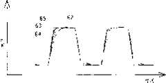
图25是后一类系统的液晶显示器中传输加到对电极电压信号线CL上的驱动电压的传输通道的等效电路图,图26是加到对电极CT上的驱动电压在所示点的每一点的波形图。Fig. 25 is an equivalent circuit diagram of the transmission channel for transmitting the driving voltage applied to the counter electrode voltage signal line CL in the liquid crystal display of the latter type of system, and Fig. 26 is a diagram showing the driving voltage applied to the counter electrode CT at each point shown One point waveform diagram.
传输加到对电极CT上的驱动电压的传输通道主要包括位于公用电压驱动器单元52和对电极电压信号线CL之间的公用总线线的电阻51、象素中的存储电容53。因此,当用交流驱动电压驱动液晶层时,从公用电压产生器和驱动器单元103的公用电压驱动器单元52传送到对电极CT的驱动电压(脉冲电压)波形会失真。The transmission channel for transmitting the drive voltage applied to the counter electrode CT mainly includes the
从图26所示的在点D的对电极电压波形54、点E的对电极电压波形55、点F的对电极电压波形56和点G的对电极电压波形57可知,随着距离的增加(从点D,到点G),加到对电极CT上的驱动电压波形的失真更严重。From the
结果是,在象素中的象素电极PX和对电极CT之间的电场不均匀,沿对电极电压信号线CL出现不规则亮度(不规则显示),而且液晶显示板的显示质量下降。As a result, the electric field between the pixel electrode PX and the counter electrode CT in the pixel becomes non-uniform, irregular luminance (irregular display) occurs along the counter electrode voltage signal line CL, and the display quality of the liquid crystal display panel deteriorates.
这是一个严重的问题,尤其是,在使用在每一水平扫描间隔之后转换加到液晶层的驱动电压的交流驱动系统时。This is a serious problem, especially when using an AC driving system that switches the driving voltage applied to the liquid crystal layer after every horizontal scanning interval.
此外,即使在一个地方断开对电极电压信号线CL时,也不能驱动液晶,因为在断开部分的后面驱动电压不能再加到象素的对电极CT上,从而使液晶显示板的显示质量下降。In addition, even when the counter electrode voltage signal line CL is disconnected at one place, the liquid crystal cannot be driven, because the driving voltage cannot be added to the counter electrode CT of the pixel behind the disconnected part, thereby deteriorating the display quality of the liquid crystal display panel. decline.
另外,按照已有技术的结构,厚度的差别是取决于引出视频信号线DL和扫描信号线GL的部分和不引出这样的信号线的部分的信号线的厚度。因此,在整个板中,间隔不规则,使液晶显示板的质量下降。In addition, according to the prior art structure, the difference in thickness depends on the thickness of the signal lines at the portion from which the video signal line DL and the scanning signal line GL are drawn and the portion from which such signal lines are not drawn. Therefore, the intervals are irregular throughout the panel, deteriorating the quality of the liquid crystal display panel.
本发明的目的是提供一种能高效率生产的高图象质量的液晶显示器,它以低压供电,消耗少量电功率,并且具有大视角特性,从而解决已有技术的上述固有问题。The object of the present invention is to provide a liquid crystal display with high image quality that can be produced efficiently, which is powered by low voltage, consumes a small amount of electric power, and has a large viewing angle characteristic, thereby solving the above-mentioned inherent problems of the prior art.
表示本说明书公开的发明的描述如下。A description representing the invention disclosed in this specification is as follows.
下面将描述解决上述第一至第四个问题的装置。Means for solving the above-mentioned first to fourth problems will be described below.
装置1
一种液晶显示器件,它具有至少一个基片是透明的两个基片,一个由两个基片夹持的液晶层以及在一个基片和液晶层之间形成的象素电极和对电极,以便通过使用在所说象素电极和所说对电极之间建立的并且有一平行于所说一个基片的分量的电场来改变液晶的透光系数和反光系数,其中,所说液晶层的电介常数各向异性量Δε、所说液晶层的有效厚度deff、所说象素电极沿短边方向的宽度Wp、所说对电极沿短边方向的宽度Wc、以及在所说象素电极和所说对电极之间的间隙L满足下述关系式:A liquid crystal display device, which has at least one of the substrates is transparent two substrates, a liquid crystal layer sandwiched by the two substrates and a pixel electrode and a counter electrode formed between a substrate and the liquid crystal layer, In order to change the transmittance and reflectance of the liquid crystal by using an electric field established between the pixel electrode and the counter electrode and having a component parallel to the one substrate, wherein the electric field of the liquid crystal layer Dielectric constant anisotropy Δε, effective thickness deff of said liquid crystal layer, width Wp of said pixel electrode along the short side direction, width Wc of said counter electrode along the short side direction, and between said pixel electrode and The gap L between said opposite electrodes satisfies the following relational expression:
Δε>0,2.8μm<deff<4.5μm,Δε>0, 2.8μm<deff<4.5μm,
1.2×deff<Wp<L/1.2,并且1.2×deff<Wc<L/1.21.2×deff<Wp<L/1.2, and 1.2×deff<Wc<L/1.2
装置2device 2
一种液晶显示器件,它具有至少一个基片是透明的两个基片,一个由两个基片夹持的液晶层以及在一个基片和液晶层之间形成的象素电极和对电极,以便通过使用在所说象素电极和所说对电极之间建立的并且有一平行于所说一个基片的分量的电场来改变液晶的透光系数和反光系数,其中,所说液晶层的电介常数各向异性量Δε、所说液晶层的有效厚度deff、所说象素电极沿短边方向的宽度Wp、所说对电极沿短边方向的宽度Wc、以及在所说象素电极和所说对电极之间的间隙L满足下述关系式:A liquid crystal display device, which has at least one of the substrates is transparent two substrates, a liquid crystal layer sandwiched by the two substrates and a pixel electrode and a counter electrode formed between a substrate and the liquid crystal layer, In order to change the transmittance and reflectance of the liquid crystal by using an electric field established between the pixel electrode and the counter electrode and having a component parallel to the one substrate, wherein the electric field of the liquid crystal layer Dielectric constant anisotropy Δε, effective thickness deff of said liquid crystal layer, width Wp of said pixel electrode along the short side direction, width Wc of said counter electrode along the short side direction, and between said pixel electrode and The gap L between said opposite electrodes satisfies the following relational expression:
Δε<0,4.2μm<deff<8.0μm,Δε<0, 4.2μm<deff<8.0μm,
1.2×deff<Wp<L/1.2,并且1.2×deff<Wc<L/1.21.2×deff<Wp<L/1.2, and 1.2×deff<Wc<L/1.2
装置3Device 3
一种液晶显示器件,它具有至少一个基片是透明的两个基片,一个由两个基片夹持的液晶层以及在一个基片和液晶层之间形成的象素电极和对电极,从而形成象素,以便通过使用在所说象素电极和所说对电极之间建立的并且有平行于所说一基片的分量的电场来改变液晶的透光系数和反光系数,并形成在一个平面上包围象素的黑色基质,其中黑色基质由绝缘材料构成。A liquid crystal display device, which has at least one of the substrates is transparent two substrates, a liquid crystal layer sandwiched by the two substrates and a pixel electrode and a counter electrode formed between a substrate and the liquid crystal layer, Pixels are thereby formed to change the transmittance and reflectance of liquid crystals by using an electric field established between said pixel electrode and said counter electrode and having a component parallel to said substrate, and formed in A black matrix that surrounds pixels on a plane, where the black matrix is made of insulating material.
装置4Device 4
一种液晶显示器件,它具有至少一个基片是透明的两个基片、一个由两个基片夹持的液晶层、一个视频信号线、一个漏电极、一个象素电极、以及一个对电极,通过漏电极和薄膜晶体管从视频信号线将视频信号加在象素电极上,在一个基片和液晶层之间形成视频信号线、漏电极、象素电极、薄膜晶体管和对电极,从而形成象素,以便通过使用在象素电极和对电极之间建立的并且有平行于所述一个基片的分量的电场来改变液晶的透光系数和反光系数,其中相邻象素的对电极定位在视频信号线的两侧,并且对电极的横向宽度不小于视频信号线宽度的一半。A liquid crystal display device having at least one substrate is transparent two substrates, a liquid crystal layer sandwiched by the two substrates, a video signal line, a drain electrode, a pixel electrode, and a counter electrode The video signal is added to the pixel electrode from the video signal line through the drain electrode and the thin film transistor, and the video signal line, the drain electrode, the pixel electrode, the thin film transistor and the counter electrode are formed between a substrate and the liquid crystal layer, thereby forming pixel so as to change the transmittance and reflectance of the liquid crystal by using an electric field established between the pixel electrode and the counter electrode and having a component parallel to the one substrate, wherein the counter electrode of the adjacent pixel is positioned On both sides of the video signal line, and the lateral width of the opposite electrode is not less than half of the width of the video signal line.
装置5Device 5
在装置4中,对电极由可阳极氧化的金属制成,并且这种金属的自身阳极氧化膜覆盖了对电极。In the device 4, the counter electrode is made of an anodizable metal, and the self anodized film of this metal covers the counter electrode.
装置6Device 6
在装置5中,对电极由铝制成。In device 5, the counter electrode was made of aluminum.
装置7Device 7
在装置5中,对电极是和栅极信号线同时形成的,由具有阳极氧化表面的一个金属层构成栅极信号线。In device 5, the counter electrode is formed simultaneously with the gate signal line, and the gate signal line is constituted by a metal layer having an anodized surface.
装置8device 8
一种液晶显示器件,它具有至少一个基片是透明的两个基片、一个由两个基片夹持的液晶层、一个视频信号线、一个漏电极、一个象素电极、一个栅极信号线、以及一个对电极,而且,通过漏电极和薄膜晶体管从视频信号线将视频信号加在象素电极上,栅极信号线与使薄膜晶体管导通的栅电极相连,通过对电压信号线将对电压加到对电极上,在一个基片和液晶层之间形成视频信号线、漏电极、象素电极、栅极信号线和对电极,从而形成象素以致通过使用在象素电极和对电极之间建立的并有平行于所述一个基片的分量的电场来改变液晶的透光系数和反光系数,其中栅极信号线由具有阳极氧化表面的金属层构成,并且对电压信号线由与栅极信号线相同的材料构成。A liquid crystal display device, which has at least one substrate is transparent two substrates, a liquid crystal layer sandwiched by the two substrates, a video signal line, a drain electrode, a pixel electrode, a gate signal line, and a counter electrode, and the video signal is added to the pixel electrode from the video signal line through the drain electrode and the thin film transistor, the gate signal line is connected to the gate electrode that makes the thin film transistor conduction, and the voltage signal line is connected to the pixel electrode. The opposite voltage is applied to the opposite electrode, and the video signal line, drain electrode, pixel electrode, gate signal line and opposite electrode are formed between a substrate and the liquid crystal layer, thereby forming a pixel so that by using the pixel electrode and the opposite electrode The electric field established between the electrodes and having a component parallel to the one substrate changes the transmittance and reflectance of the liquid crystal, wherein the grid signal line is made of a metal layer having an anodized surface, and the voltage signal line is composed of It is composed of the same material as the gate signal line.
装置9device 9
在装置8中,对电压信号线由铝制成。In device 8, the pair voltage signal line is made of aluminum.
装置10device 10
在装置8中,对电压信号线和栅极信号线是通过相同的步骤形成的。In device 8, the pair voltage signal lines and the gate signal lines are formed through the same steps.
装置11device 11
一种液晶显示器件,它具有至少一个基片是透明的两个基片、一个夹在两个基片间的液晶层、一个视频信号线、一个漏电极、一个象素电极、一个使薄膜晶体管导通的栅电极、一个对电极、以及一个存贮电容器,通过漏电极和薄膜晶体管从视频信号线将视频信号加在象素电极上,通过对电压信号线将对电压加到对电极上,通过一个经过层间绝缘膜在部分对电极电压信号线上叠加部分象素电极而形成电容器,在一个基片和液晶层之间形成视频信号线、漏电极、象素电极、栅电机、对电极以及存贮电容器,从而形成象素以致通过使用在象素电极和对电极之间建立的并且有平行于所述一个基片的分量的电场来改变液晶的透光系数和反光系数,其中对电极电压信号线由具有阳极氧化表面的铝制成。A liquid crystal display device, which has at least one substrate is transparent two substrates, a liquid crystal layer sandwiched between the two substrates, a video signal line, a drain electrode, a pixel electrode, a thin film transistor Conducted gate electrode, a counter electrode, and a storage capacitor, the video signal is applied to the pixel electrode from the video signal line through the drain electrode and the thin film transistor, and the counter voltage is applied to the counter electrode through the counter voltage signal line, A capacitor is formed by superimposing a part of the pixel electrode on a part of the counter electrode voltage signal line through an interlayer insulating film, and a video signal line, a drain electrode, a pixel electrode, a gate motor, and a counter electrode are formed between a substrate and a liquid crystal layer. and a storage capacitor, thereby forming a pixel such that the transmittance and reflectance of the liquid crystal are changed by using an electric field established between the pixel electrode and the counter electrode and having a component parallel to the one substrate, wherein the counter electrode The voltage signal wires are made of aluminum with an anodized surface.
装置12device 12
一种液晶显示器件,它具有至少一个基片是透明的两个基片、一个夹在两个基片之间的液晶层、一个视频信号线、一个漏电极、一个象素电极、一个使薄膜晶体管导通的栅电极、以及一个对电极,视频信号线、漏电极、象素电极、栅电极以及对电极都是在所述一个基片和液晶层之间形成的,通过漏电极和薄膜晶体管从视频信号线将视频信号加到象素电极上,通过对电极电压信号线将对电极电压加到对电极上,从而形成象素以致通过使用在象素电极和对电极之间建立的并且有平行于所说一个基片的分量的电场来改变液晶的透光系数和反光系数,其中设置一个公用总线以连接多个象素的所有对电极电压信号线,并且该公用总线为由两个或三个导电层构成的一个多层结构。A liquid crystal display device, which has at least one substrate is transparent two substrates, a liquid crystal layer sandwiched between the two substrates, a video signal line, a drain electrode, a pixel electrode, a thin film The gate electrode for the conduction of the transistor and a counter electrode, the video signal line, the drain electrode, the pixel electrode, the gate electrode and the counter electrode are all formed between the one substrate and the liquid crystal layer, through the drain electrode and the thin film transistor A video signal is applied to a pixel electrode from a video signal line, and an opposite electrode voltage is applied to an opposite electrode through an opposite electrode voltage signal line, thereby forming a pixel so that by using a circuit established between the pixel electrode and the opposite electrode and having Parallel to the electric field of the component of said a substrate to change the transmittance and reflectance of the liquid crystal, wherein a common bus is set to connect all the opposite electrode voltage signal lines of a plurality of pixels, and the common bus is composed of two or A multilayer structure consisting of three conductive layers.
装置13device 13
在装置12中,其中公用总线线由两个导电层构成,一个导电层的材料与栅极的材料相同,另一个导电层的材料与视频信号线的材料相同,这两个导电层是在形成栅极和视频信号线的同时形成的。In the device 12, wherein the common bus line is composed of two conductive layers, the material of one conductive layer is the same as the material of the grid, and the material of the other conductive layer is the same as that of the video signal line, these two conductive layers are formed Gate and video signal lines are formed simultaneously.
为了解决本发明的上述第五个问题,在列方向上彼此相邻的两个象素共用对电极电压信号线和漏极电压,并且在一部分对电极电压信号线中形成存贮电容器。In order to solve the above-mentioned fifth problem of the present invention, two pixels adjacent to each other in the column direction share the counter electrode voltage signal line and the drain voltage, and a storage capacitor is formed in a part of the counter electrode voltage signal line.
装置14device 14
一种液晶显示器件,它具有至少一个基片是透明的两个基片,一个夹在两个基片之间的液晶层、一个视频信号线、一个漏电极、一个象素电极、一个使薄膜晶体管导通的栅电极、一个对电极、以及一个存贮电容器,视频信号线、漏电极、象素电极、栅电极、薄膜晶体管、对电极以及存贮电容器都是在所述一个基片和液晶层之间形成的,通过漏电极和薄膜晶体管从视频信号线将视频信号加到象素电极上,通过对电极电压信号线将对电极电压加到对电极极上,通过一个层间绝缘膜在部分对电极电压信号线上叠加部分象素电极而形成电容器,从而形成象素,以致于通过使用在象素电极和对电极之间建立的并且有平行于所述一个基片的一分量的电场来改变液晶的透光系数和反光系数,其中,把连接到所述栅极的栅极信号线和连接到对电极的对电极电压信号线安排成平行于按矩阵形式排列的多个象素的第一方向,并且把连接到漏极的视频信号线安排成平行于该多个象素的第二方向;并且在第二方向的两个彼此相邻的象素公用对电极电压信号线。A liquid crystal display device, which has at least one substrate is transparent two substrates, a liquid crystal layer sandwiched between the two substrates, a video signal line, a drain electrode, a pixel electrode, a thin film The gate electrode, a counter electrode, and a storage capacitor for transistor conduction, the video signal line, the drain electrode, the pixel electrode, the gate electrode, the thin film transistor, the counter electrode, and the storage capacitor are all on the substrate and the liquid crystal. Formed between the layers, the video signal is added to the pixel electrode from the video signal line through the drain electrode and the thin film transistor, and the opposite electrode voltage is applied to the opposite electrode through the opposite electrode voltage signal line, and an interlayer insulating film is used in the Part of the counter electrode voltage signal line superimposes part of the pixel electrode to form a capacitor, thereby forming a pixel, so that by using an electric field that is established between the pixel electrode and the counter electrode and has a component parallel to the one substrate To change the transmittance and reflectance of the liquid crystal, wherein the gate signal line connected to the grid and the counter electrode voltage signal line connected to the counter electrode are arranged parallel to the multiple pixels arranged in a matrix the first direction, and arrange the video signal line connected to the drain to be parallel to the second direction of the plurality of pixels; and two adjacent pixels in the second direction share the opposite electrode voltage signal line.
装置15Device 15
在装置14中,对沿列方向彼此相邻的两个象素的栅极、栅极信号线、和薄膜晶体管元件进行安排,以使它们彼此相对,由两个象素公用漏极,而且将从漏极到视频信号线的连线安排在相对的两个扫描信号线之间。In the device 14, the gates, gate signal lines, and thin film transistor elements of two pixels adjacent to each other in the column direction are arranged so that they face each other, the common drain is shared by the two pixels, and the The wiring from the drain to the video signal line is arranged between two opposite scanning signal lines.
装置16
在装置15中,按多个薄膜晶体管都连接在一个象素中的象素电极上的方式沿扫描信号线形成薄膜晶体管。In the device 15, thin film transistors are formed along the scanning signal line in such a manner that a plurality of thin film transistors are connected to the pixel electrode in one pixel.
下面将描述解决上述第六个问题的装置。Means for solving the above sixth problem will be described below.
装置17Device 17
一种液晶显示器件,它具有至少一个基片是透明的两个基片、夹在两个基片之间的一个液晶层、一个视频信号线、一个漏电极、一个象素电极、一个与使薄膜晶体管导通的栅电极相连的栅极信号线和一个对电极,视频信号线、漏电极、象素电极、栅极信号线和对电极都是在一个基片和液晶层之间形成的,通过漏电极和薄膜晶体管从视频信号线将视频信号加到象素电极上,通过对电极电压信号线将对电极电压加到对电极上,借此形成象素以致通过使用在象素电极和对电极之间建立的并且具有一个平行于基片的分量的电场来改变液晶的透光系数和反光系数,其中,对电极电压信号线两侧的端部连接到一个公用总线线上,并且进一步还连接到一个公用电压产生和驱动装置上。A liquid crystal display device, which has at least one substrate is transparent two substrates, a liquid crystal layer sandwiched between the two substrates, a video signal line, a drain electrode, a pixel electrode, a The gate signal line connected to the gate electrode of the thin film transistor and a counter electrode, the video signal line, the drain electrode, the pixel electrode, the gate signal line and the counter electrode are all formed between a substrate and the liquid crystal layer, The video signal is applied to the pixel electrode from the video signal line through the drain electrode and the thin film transistor, and the opposite electrode voltage is applied to the opposite electrode through the opposite electrode voltage signal line, thereby forming a pixel so that by using the pixel electrode and the opposite electrode An electric field established between the electrodes and having a component parallel to the substrate changes the transmittance and reflectance of the liquid crystal, wherein the ends on both sides of the electrode voltage signal line are connected to a common bus line, and further Connect to a common voltage generating and driving device.
装置18device 18
在装置17中,在一个基片的非显示区上形成厚度调节图案,厚度调节图案由和公用总线线相同的材料制成,并且厚度也相同。In the device 17, a thickness adjusting pattern is formed on a non-display area of a substrate, the thickness adjusting pattern is made of the same material as the common bus line and has the same thickness.
装置19Device 19
在装置17或18中,在除了公共总线线和栅极信号线或视频信号线交叉的区域以外,并且除了公用总线线与对电极电压信号线相连的区域以外的非交叉区中的公用总线的上方或下方设置一个厚度调节膜,该膜的材料和厚度都与栅极的材料和厚度相同。In the device 17 or 18, except for the area where the common bus line crosses the gate signal line or the video signal line, and except for the area where the common bus line is connected to the counter electrode voltage signal line, the common bus line in the non-crossing area A thickness adjusting film is arranged above or below, and the material and thickness of the film are the same as those of the grid.
装置20device 20
在装置17或18中,在除了公共总线线和栅极信号线或视频信号线交叉的区域以外、并且除了公用总线线与对电极电压信号线相连的区域以外的非交叉区中的公用总线的上方或下方设置一个厚度调节膜,该膜的材料和厚度都与漏极的材料和厚度相同。In the device 17 or 18, the common bus line in the non-intersection area except the area where the common bus line crosses the gate signal line or the video signal line, and except the area where the common bus line is connected to the counter electrode voltage signal line A thickness adjusting film is arranged above or below, and the material and thickness of the film are the same as those of the drain electrode.
按照装置1的结构,当使用具有正的各向异性介电常数的液晶混合物时,能获得几乎与二次光折射模式的波长无关的透射特性,即能获得良好的白色显示,并且能将电场强度比垂于于基片方向上的电场分量大得多的平行于基片的电场分量加到液晶层上。从而,能利用最有效的透射状态,使象素电极和对电极之间的电压能有效地转换成与基片平行的方向上的分量,而不引起驱动液晶的电压增加。According to the structure of the
按照装置2的结构,当使用具有负的各同异性介电常数的液晶混合物时,能获得几乎与二次光折射模式的波长无关的透光特性,即能获得良好的白色显示,而且能将电场强度比垂于于基片方向上的电场分量大得多的平行于基片的电场分量加到液晶层上。因而能利用最有效的透射状态,使象素电极和对电极之间的电压能有效地转换成与基片平行的方向上的分量,而不引起驱动液晶的电压上升。According to the structure of the device 2, when using a liquid crystal mixture with a negative anisotropic dielectric constant, light transmission characteristics that are almost independent of the wavelength of the secondary light refraction mode can be obtained, that is, good white display can be obtained, and the An electric field component parallel to the substrate whose electric field strength is much greater than that perpendicular to the substrate is applied to the liquid crystal layer. Therefore, the most effective transmission state can be used, so that the voltage between the pixel electrode and the counter electrode can be effectively converted into a component in the direction parallel to the substrate, without causing the voltage for driving the liquid crystal to rise.
按照装置3的结构,由于由绝缘材料构成黑色基质,因而能消除对象素电极和对电极之间的电场的影响。黑色基质遮断了对能使电极间的距离减小的在象素电极和对电极之间的电场的影响。因而,容许增加孔径比,并且,在不增加驱动液晶的电压的情况下,能有效地将平行于基片表面的电场分量加到液晶层上。According to the structure of the device 3, since the black matrix is made of an insulating material, the influence of the electric field between the pixel electrode and the counter electrode can be eliminated. The black matrix blocks the influence of the electric field between the pixel electrode and the counter electrode which enables the distance between the electrodes to be reduced. Thus, the aperture ratio is allowed to be increased, and the electric field component parallel to the substrate surface can be efficiently applied to the liquid crystal layer without increasing the voltage for driving the liquid crystal.
按照装置4的结构,来自视频信号线的电力线能被位于其两边的对电极吸收,从而能防止通常所说的交叉干扰的出现。在这种情况下,由两侧的对电极各吸收50%的来自视频信号线的电力线,即,总共吸收了100%的电力线。According to the structure of the device 4, the electric power lines from the video signal lines can be absorbed by the counter electrodes located on both sides thereof, so that the occurrence of so-called cross-talk can be prevented. In this case, 50% of the lines of electric force from the video signal lines are absorbed by the opposing electrodes on both sides, ie, 100% of the lines of electric force are absorbed in total.
按照装置5的结构,即使在使两边的对电极彼此尽可能靠近时,或者即使在将它们设计成与视频信号线相交时,也能防止短路出现。从而能增加孔径比。According to the structure of the device 5, even when the opposing electrodes on both sides are brought as close as possible to each other, or even when they are designed to intersect the video signal lines, occurrence of a short circuit can be prevented. Thus, the aperture ratio can be increased.
按照装置6的结构,对电极有较小的电阻。所以,基本上均匀并稳定的电流流经对电极,而且,将对电极电压很平稳地传输到终端的象素上,从而能进一步地提高装置4的效果。According to the structure of the device 6, the counter electrode has a lower resistance. Therefore, a substantially uniform and stable current flows through the counter electrode, and the counter electrode voltage is transmitted very smoothly to the terminal pixels, so that the effect of the device 4 can be further enhanced.
按照装置7的结构,在不增加生产步骤数的情况下,能获得装置5的效果。According to the structure of the device 7, the effect of the device 5 can be obtained without increasing the number of production steps.
按照装置8的结构,能减少在对电极电压信号线与视频信号线相交的区域中的短路概率。According to the structure of the device 8, the probability of short circuit in the area where the counter voltage signal line intersects with the video signal line can be reduced.
按照装置9的结构,对电极电压信号线的电阻较小,而且基本上均匀并稳定的电流流过每一个对电极。因而,足以将对电极电压传输到终端的象素上,能实现均匀的象素显示。According to the structure of the device 9, the resistance of the counter electrode voltage signal line is small, and a substantially uniform and stable current flows through each counter electrode. Therefore, it is sufficient to transmit the counter-electrode voltage to the pixels at the terminals, and uniform pixel display can be realized.
按照装置10的结构,在不增加生产步骤数量的情况下,能获得装置7的效果。According to the structure of the apparatus 10, the effect of the apparatus 7 can be obtained without increasing the number of production steps.
按照装置11的结构,通过层间绝缘膜形成的下边的电极由具有阳极氧化表面的铝制成,从而,能形成存贮电容器,几乎不会出现通常所说的晶须引起的点缺陷所产生的问题。According to the structure of the device 11, the lower electrode formed by the interlayer insulating film is made of aluminum having an anodized surface, thereby, a storage capacitor can be formed, and the generation of point defects caused by so-called whiskers hardly occurs. The problem.
按照装置12的结构,能减少电阻而不增加公用总线线的宽度,并且将足够高的电压加到对电极端上。从而能减少由根据视频信号的对电极电压的失真而引起交叉干扰(特别是,在屏幕的水平方向)。According to the structure of the device 12, the resistance can be reduced without increasing the width of the common bus line, and a sufficiently high voltage can be applied to the opposite electrode terminal. It is thereby possible to reduce crosstalk (in particular, in the horizontal direction of the screen) caused by distortion of the counter-electrode voltage according to the video signal.
按照装置13的结构,能获得装置12的效果而不增加生产步骤数。According to the structure of the device 13, the effect of the device 12 can be obtained without increasing the number of production steps.
按照装置14的结构,使连接到栅极GT的栅极信号线GL和连接到对电极CT的对电极电压信号线CT平行于按矩阵形式排列的多个象素的行方向,列方向上彼此相邻的两个象素公用对电极电压信号线CL,并且使连接到漏极SD2的视频信号线DL平行于列方向,从而减少引线中的寄生电容、提高生产产量、保证象素中的开口以及减少对电极电压信号线CL的电阻。According to the structure of the device 14, the gate signal line GL connected to the gate GT and the counter electrode voltage signal line CT connected to the counter electrode CT are parallel to the row direction of a plurality of pixels arranged in a matrix form, and mutually connected to each other in the column direction. Two adjacent pixels share the opposite electrode voltage signal line CL, and make the video signal line DL connected to the drain electrode SD2 parallel to the column direction, thereby reducing the parasitic capacitance in the lead wire, improving production yield, and ensuring the opening in the pixel And reduce the resistance of the electrode voltage signal line CL.
按照装置15的结构,将装置14的结构中沿列方向彼此相邻的两个象素的栅极GT、栅极信号线GL、和薄膜晶体管元件设置成彼此相对,两个象素公用漏极SD2,并将从漏极SD2到视频信号线DL的连线安排在相对的栅极信号线GL之间,从而减少连线中的寄生电容、提高生产产量、保证象素中的开口、和减少对电极电压信号线CL的电阻。According to the structure of device 15, the gate GT, gate signal line GL and thin film transistor elements of two pixels adjacent to each other along the column direction in the structure of device 14 are arranged to be opposite to each other, and the common drain of two pixels SD2, and the connection from the drain SD2 to the video signal line DL is arranged between the opposite gate signal lines GL, thereby reducing the parasitic capacitance in the connection, improving production yield, ensuring the opening in the pixel, and reducing The resistance of the electrode voltage signal line CL.
按照装置16的结构,沿栅极信号线GL形成薄膜晶体管,使得多个薄膜晶体管与装置15的结构的一个象素的象素电极PX相连,从而减少连线中的寄生电容、提高生产量、保证象素中的开口、和减小对电极电压信号线CL的电阻。According to the structure of the
按照装置17至20的结构,对电极电压信号线CL的两端与公用总线线CB相连,共用总线线CB的电阻比对电极电压信号线CL的电阻小。因而能减少从公用电压驱动器单元52加到对电极CT上的驱动电压的波形的失真、使在面板中每一象素的象素电极PX和对电极CT之间的电场强度均匀、和减少沿对电极电压信号线CL出现的亮度不均匀性。According to the structures of devices 17 to 20, both ends of the counter electrode voltage signal line CL are connected to the common bus line CB, and the resistance of the common bus line CB is smaller than that of the counter electrode voltage signal line CL. Therefore, it is possible to reduce the distortion of the waveform of the driving voltage applied to the counter electrode CT from the common
即使在对电极电压信号线CL部分断开的情况下,也能由对电极电压信号线CL的两端提供公用电压,从而驱动象素的液晶,因此,与已有技术不同,能驱动有断开部分的象素的液晶,而且显示质量不变。Even when the counter-electrode voltage signal line CL is partially disconnected, a common voltage can be provided from both ends of the counter-electrode voltage signal line CL to drive the liquid crystal of the pixel. The liquid crystal of the pixel of the open part, and the display quality does not change.
此外,设置了公用总线线CB的区域与公用总线线CB和栅极信号线GL或视频信号DL相交的区域有相同的横截面结构,从而能减少在形成公用总线线CB的基片边缘处膜厚度的不均匀性、使两个基片之间的间隙长度均匀、和减少液晶显示器件的间隙不均匀性。In addition, the area where the common bus line CB is provided has the same cross-sectional structure as the area where the common bus line CB intersects with the gate signal line GL or the video signal DL, so that the film at the edge of the substrate where the common bus line CB is formed can be reduced. Non-uniformity of thickness, uniformity of gap length between two substrates, and reduction of gap non-uniformity of liquid crystal display devices.
由下面参照附图的详细描述将理解本发明的上述和其它目的、优点、工作方式和新颖的特征。The above and other objects, advantages, modes of operation and novel features of the present invention will be understood from the following detailed description with reference to the accompanying drawings.
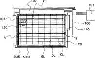
图1是描述一个象素的示意图,用于解释本发明液晶显示单元的基本操作;Fig. 1 is a schematic diagram describing a pixel for explaining the basic operation of the liquid crystal display unit of the present invention;
图2是平面图,描述在实施例1的有源矩阵型彩色液晶显示器件的液晶显示单元中的一个象素和其周围的主要部件;Fig. 2 is a plan view describing a pixel and its surrounding main parts in the liquid crystal display unit of the active matrix type color liquid crystal display device of
图3是描述实施例1的黑色基质的图案的图;3 is a diagram describing the pattern of the black matrix of Example 1;
图4是描述在实施例2的有源矩阵型彩色液晶显示器件的液晶显示单元中一个象素和其周围部分的主要部件的平面图;Fig. 4 is the plan view that describes a pixel and its surrounding parts in the liquid crystal display unit of the active matrix type color liquid crystal display device of embodiment 2;
图5是在实施例1的象素形成的液晶显示板上的多个象素的平面图;Fig. 5 is the plan view of a plurality of pixels on the liquid crystal display panel that the pixel of
图6是在实施例1的列方向上彼此相邻的两个象素的等效电路图;6 is an equivalent circuit diagram of two pixels adjacent to each other in the column direction of
图7是沿图2的线3-3的一个象素的剖面图;Figure 7 is a cross-sectional view of a pixel along line 3-3 of Figure 2;
图8是沿图2的线-剖开的一个薄膜晶体管元件TFT的剖面图;Fig. 8 is a cross-sectional view of a thin film transistor element TFT cut along the line of Fig. 2;
图9是沿图2的线5-5剖开的一个存贮电容器Cstg的横截面图;Fig. 9 is a cross-sectional view of a storage capacitor Cstg taken along line 5-5 of Fig. 2;
图10是用于解释显示板的矩阵周围结构的平面图;10 is a plan view for explaining the structure around the matrix of the display panel;
图11是一个横截面图,描述在左边有栅极信号端而在右边没有外部连接端的板边缘部分;Figure 11 is a cross-sectional view depicting the edge portion of the board with gate signal terminals on the left and no external connection terminals on the right;
图12A和12B是描述栅极端GTM与栅极连线GL相连的区域的平面图和横截面图;12A and 12B are plan views and cross-sectional views describing a region where the gate terminal GTM is connected to the gate line GL;
图13A和13B是描述漏极端DTM与视频信号线DL相连的区域的平面图和横截面图;13A and 13B are a plan view and a cross-sectional view describing a region where the drain terminal DTM is connected to the video signal line DL;
图14A和14B是描述公用电极端CTM、公用总线线CB和公用电压信号线CL连接在一起的区域的平面图和横截面图;14A and 14B are plan views and cross-sectional views describing a region where the common electrode terminal CTM, the common bus line CB and the common voltage signal line CL are connected together;
图15是描述制作基片SUB1的步骤A至C的一个象素和栅极端的剖面图的流程图;Fig. 15 is a flow chart describing the sectional view of a pixel and gate terminal of steps A to C of making substrate SUB1;
图16是描述制作基片SUB1的步骤D至F的象素和栅极端的剖面图的流程图;Fig. 16 is a flow chart describing the cross-sectional views of pixels and gate terminals of steps D to F of making substrate SUB1;
图17是象素和栅极端的剖面图的流程图,描述制作基片SUB1的步骤G至H;Fig. 17 is the flow chart of the sectional view of pixel and gate end, describes the steps G to H of making substrate SUB1;
图18是描述施加电场的方向、摩擦方向以及偏振板的透射轴之间的相互关系的图;Fig. 18 is a graph describing the relationship between the direction of the applied electric field, the rubbing direction, and the transmission axis of the polarizing plate;
图19是描述本发明有源矩阵型彩色液晶显示器件的矩阵单元和其外围部分的电路图;Fig. 19 is a circuit diagram describing the matrix unit and its peripheral parts of the active matrix type color liquid crystal display device of the present invention;
图20是描述驱动本发明有源矩阵型彩色液晶显示器件的波形的曲线图;Fig. 20 is a graph describing waveforms for driving the active matrix type color liquid crystal display device of the present invention;
图21是描述外围驱动单元装在液晶显示板上的顶视图;Fig. 21 is a top view describing that the peripheral drive unit is mounted on the liquid crystal display panel;
图22是描述带式封装组件TCP(用横截面图)结构的图,用TCP将构成驱动单元的集成电路芯片CHI安装在软性接线基片上;22 is a diagram describing the structure of the tape package TCP (with a cross-sectional view), and the integrated circuit chip CHI constituting the drive unit is installed on the flexible wiring substrate with the TCP;
图23是一个剖面图,描述在TCP连接到液晶显示板PNL的栅极信号电路的端部GTM上的情况下的主要部件;FIG. 23 is a sectional view illustrating the main parts in the case where the TCP is connected to the terminal GTM of the gate signal circuit of the liquid crystal display panel PNL;
图24是描述液晶显示组件的立体图;Fig. 24 is a perspective view illustrating a liquid crystal display assembly;
图25是在图19的液晶显示器件中将驱动电压传送到对电极CT上的通路的等效电路图;Fig. 25 is an equivalent circuit diagram of the path for transmitting the driving voltage to the counter electrode CT in the liquid crystal display device of Fig. 19;
图26是特性曲线图,描述图25所示的每一点的驱动电压波形;Fig. 26 is a characteristic curve diagram describing the driving voltage waveform of each point shown in Fig. 25;
图27是描述实施例3的液晶显示器件的结构的示意方框图;27 is a schematic block diagram describing the structure of a liquid crystal display device of Embodiment 3;
图28是在实施例3的液晶显示器件中将驱动电压传输到对电极CT上的通路的等效电路图;Fig. 28 is an equivalent circuit diagram of the path for transmitting the drive voltage to the counter electrode CT in the liquid crystal display device of Embodiment 3;
图29是描述图28所示的每一点的驱动电压波形的特性曲线图;Fig. 29 is a characteristic graph describing the driving voltage waveform of each point shown in Fig. 28;
图30A至30C是表示在图27的矩阵基片上的点A处连接对电极电压信号线CL和公用总线线CB的平面图和剖面图;30A to 30C are plan views and cross-sectional views showing that the point A on the matrix substrate of FIG. 27 is connected to the electrode voltage signal line CL and the common bus line CB;
图31A和31B是描述在图27的矩阵基片上的点B处连接对电极电压信号线CL和公用总线线CB的平面图和剖面图;31A and 31B are a plan view and a sectional view of connecting the opposite electrode voltage signal line CL and the common bus line CB at point B on the matrix substrate of FIG. 27;
图32A和32B是平面图和剖面图,描述在图27的矩阵基片上的点C处视频信号线DL和公用总线线CB相交;32A and 32B are a plan view and a sectional view, describing the intersection of the video signal line DL and the common bus line CB at point C on the matrix substrate of FIG. 27;
图33A至33C是平面图和剖面图,描述在图27的矩阵上的点A处对电极电压信号线CL和公用总线线CB相连的另一例子;33A to 33C are plan views and sectional views illustrating another example of connecting electrode voltage signal lines CL and common bus lines CB at point A on the matrix of FIG. 27;
图34是描述实施例3的公用总线线CB的另一种布线的平面图;34 is a plan view illustrating another wiring of the common bus line CB of Embodiment 3;
图35是描述实施例3的公用总线线CB的又一种布线的平面图;FIG. 35 is a plan view illustrating yet another wiring of the common bus line CB of Embodiment 3;
图36A至36C是平面图和剖面图,描述在实施例4的液晶显示器件中在与图27的矩阵基片上的点A对应的点上连接对电极电压信号线CL和公用总线线CB;36A to 36C are plan views and sectional views, describing the connection of the counter electrode voltage signal line CL and the common bus line CB at a point corresponding to point A on the matrix substrate of FIG. 27 in the liquid crystal display device of Embodiment 4;
图37A和37B是平面图和剖面图,描述在实施例4的液晶显示器件中在与图27的矩阵基片上的点B对应的点上连接对电极电压信号线CL和公用总线线CB;37A and 37B are plan views and sectional views, describing the connection of the counter electrode voltage signal line CL and the common bus line CB at the point corresponding to point B on the matrix substrate of FIG. 27 in the liquid crystal display device of embodiment 4;
图38A和38B是平面图和剖面图,描述在实施例4的液晶显示器件中在与图27的矩阵基片上的点C对应的点上视频信号线DL和公用总线线CB相交;以及38A and 38B are plan views and sectional views illustrating intersections of video signal lines DL and common bus lines CB at points corresponding to point C on the matrix substrate of FIG. 27 in the liquid crystal display device of Embodiment 4; and
图39是描述实施例4的公用总线线CB的另一种布线的平面图。FIG. 39 is a plan view illustrating another wiring of the common bus line CB of Embodiment 4. FIG.
由下面参考附图的描述,本发明的进一步目的和特征将变得很清楚。Further objects and features of the present invention will become apparent from the following description with reference to the accompanying drawings.
[有源矩阵液晶显示器件][Active Matrix Liquid Crystal Display Devices]
下面描述本发明适合有源矩阵系统的彩色液晶显示器件的实施例。在附图中,用相同的标号表示具有相同功能的那些部件,而且不重复描述它们。Embodiments of the color liquid crystal display device of the present invention suitable for an active matrix system are described below. In the drawings, those components having the same functions are denoted by the same reference numerals, and their descriptions are not repeated.
在描述本发明实施例之间,首先,解释本发明适用的液晶显示单元的基本操作。Before describing the embodiments of the present invention, first, the basic operation of the liquid crystal display unit to which the present invention is applied is explained.
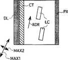
图1A至1D是一个象素的示意图,用于解释本发明适用的液晶显示单元的操作,其中,图1A是不加电压时的剖面图,图1B是加电压时的剖面图,图1C是不加电压时的平面图,图1D是加电压时的平面图。在这些附图中,SUB1和SUB2代表透明玻璃基片(以后常简称为基片),CT代表对电极,GI代表绝缘膜,DL代表视频信号线,PX代表象素电极,POL1和POL2代表偏振器板,MAX1代表下偏振器板的极化轴,MAX2代表上偏振器板的极化轴,RDR代表液晶分子的初始取向,EDR代表电场的方向,BM代表黑色基质,FIL代表滤色片,OC代表补偿膜,ORI1和ORI2代表取向膜,LC代表液晶(圆棒形液晶分子)。1A to 1D are schematic diagrams of a pixel for explaining the operation of a liquid crystal display unit to which the present invention is applicable, wherein FIG. 1A is a sectional view when no voltage is applied, and FIG. The plan view when no voltage is applied, and Figure 1D is the plan view when voltage is applied. In these drawings, SUB1 and SUB2 represent transparent glass substrates (hereinafter often referred to as substrates), CT represents counter electrodes, GI represents insulating films, DL represents video signal lines, PX represents pixel electrodes, and POL1 and POL2 represent polarization MAX1 represents the polarization axis of the lower polarizer plate, MAX2 represents the polarization axis of the upper polarizer plate, RDR represents the initial orientation of liquid crystal molecules, EDR represents the direction of the electric field, BM represents the black matrix, FIL represents the color filter, OC stands for compensation film, ORI1 and ORI2 stand for alignment film, and LC stands for liquid crystal (rod-shaped liquid crystal molecules).
在液晶显示单元中,在两个透明玻璃基片SUB1和SUB2的一个基片SUB2上形成偏振器板POL2、遮光黑色基质BM、滤色片FIL、保护膜OC以及取向膜ORI2。穿过液晶LC,在另一基片SUB1上形成偏振器板POL1、取向膜ORI1、漏极SD2、象素电极PX、对电极CT、接线和薄膜晶体管。这些附图都没有图示出接线和薄膜晶体管。In the liquid crystal display unit, a polarizer plate POL2, a light-shielding black matrix BM, a color filter FIL, an overcoat film OC, and an alignment film ORI2 are formed on one substrate SUB2 of two transparent glass substrates SUB1 and SUB2. Through the liquid crystal LC, a polarizer plate POL1, an orientation film ORI1, a drain electrode SD2, a pixel electrode PX, a counter electrode CT, wiring and a thin film transistor are formed on another substrate SUB1. None of these drawings show wiring and thin film transistors.
参见图1A和1C,已事先由取向膜ORI1和ORI2使液晶LC沿基本上与基片SUB1表面平行的取向RDR上取向。在此状态下,液晶LC的初始取向RDR几乎与偏振板POL1的极化轴MAX1一致,极化轴MAX1和另一偏振板POL2的极化轴MAX2垂直相交,而且象素处于非显示状态。Referring to FIGS. 1A and 1C, the liquid crystal LC has been previously aligned in the orientation RDR substantially parallel to the surface of the substrate SUB1 by the orientation films ORI1 and ORI2. In this state, the initial orientation RDR of the liquid crystal LC almost coincides with the polarization axis MAX1 of the polarizing plate POL1, which perpendicularly intersects the polarization axis MAX2 of the other polarizing plate POL2, and the pixel is in a non-displaying state.
接下来,参见图1B和1D,当在玻璃基片SUB1上形成的对电极CT和象素电极PX之间施加电压以形成基本上与基片SUB1的表面平行的电场(有一方向EDR)时,使液晶分子LC在基本上与基片SUB1的表面平行的平面内发生扭曲。然后,象素变为显示状态。设置大量的象素来构成一个显示板。Next, referring to FIGS. 1B and 1D, when a voltage is applied between the counter electrode CT formed on the glass substrate SUB1 and the pixel electrode PX to form an electric field substantially parallel to the surface of the substrate SUB1 (with a direction EDR), The liquid crystal molecules LC are twisted in a plane substantially parallel to the surface of the substrate SUB1. Then, the pixel becomes a display state. A large number of pixels are set to constitute a display panel.
[矩阵单元(象素单元)的平面结构][Plane Structure of Matrix Unit (Pixel Unit)]
图2是一个平面图,描述本发明第一实施例的有源矩阵型彩色液晶显示器件中的一个象素和其外围部分。Fig. 2 is a plan view illustrating a pixel and its peripheral portion in the active matrix type color liquid crystal display device of the first embodiment of the present invention.
参见图2,每一象素都设置在栅极信号线(栅极信号线或水平信号线)GL、对电极电压信号线(对电极接线)CL和两个相邻视频信号线(漏极信号线或垂直信号线)DL相交的一个区域内。每一象素包括一个薄膜晶体管TFT、一个存贮电容器Cstg、一个象素电极PX和一个对电极CT。在附图中,栅极信号线GL和对电极电压信号线CL沿左、右方向延伸,并且沿上、下方向设置了大量的栅极信号线GL和对电极电压信号线CL。视频信号线DL沿上、下方向延伸,并且沿左右方向安排了大量的视频信号线DL。象素电极PX与薄膜晶体管TFT相连,而且对电极CT与对电极电压信号线CL一体形成。Referring to Fig. 2, each pixel is arranged on the gate signal line (gate signal line or horizontal signal line) GL, the opposite electrode voltage signal line (opposite electrode connection) CL and two adjacent video signal lines (drain signal line) line or vertical signal line) in an area where DL intersects. Each pixel includes a thin film transistor TFT, a storage capacitor Cstg, a pixel electrode PX and a counter electrode CT. In the drawing, gate signal lines GL and counter voltage signal lines CL extend in left and right directions, and a large number of gate signal lines GL and counter voltage signal lines CL are arranged in up and down directions. The video signal lines DL extend in the upper and lower directions, and a large number of video signal lines DL are arranged in the left and right directions. The pixel electrode PX is connected to the thin film transistor TFT, and the counter electrode CT is integrally formed with the counter electrode voltage signal line CL.
沿视频信号线DL的两相邻象素为平面结构使得它们具有相同的尺寸和图案。其理由是:沿视频信号线DL的两个纵向的相邻的象素公用对电极电压信号线CL,使对电极电压信号线CL的宽度减小,从而使对电极电压信号线CL的电阻减小。能容易地从外电路向沿左、右方向安排的象素的对电极CT充分馈送对电极电压。Two adjacent pixels along the video signal line DL have a planar structure so that they have the same size and pattern. The reason is: two adjacent pixels along the vertical direction of the video signal line DL share the opposite electrode voltage signal line CL, so that the width of the opposite electrode voltage signal line CL is reduced, thereby reducing the resistance of the opposite electrode voltage signal line CL. Small. The counter electrode voltage can be easily supplied from the external circuit to the counter electrodes CT of the pixels arranged in the left and right directions sufficiently.
使象素电极PX和对电极CT彼此相对而置,并且由每一象素电极PX和对电极CT之间的电场控制液晶LC的光学状态,进而控制显示。制成象梳齿一样的象素电极PX和对电极CT,而且象素电极PX和对电极CT沿上、下方向以细长形式延伸。The pixel electrode PX and the counter electrode CT are placed opposite to each other, and the optical state of the liquid crystal LC is controlled by the electric field between each pixel electrode PX and the counter electrode CT, thereby controlling display. The pixel electrode PX and the counter electrode CT are formed like comb teeth, and the pixel electrode PX and the counter electrode CT extend in an elongated form in the upper and lower directions.
当在同一基片的表面上安排象素电极PX和对电极CT时,与在列方向上彼此相邻的两个象素不共用对电极电压信号线CL的接线结构相比,本实施例的液晶显示单元能增加透射光的象素开孔部分的面积并且能增加对电极电压信号线CL的宽度。When the pixel electrode PX and the counter electrode CT are arranged on the surface of the same substrate, compared with the wiring structure in which two pixels adjacent to each other in the column direction do not share the counter electrode voltage signal line CL, the present embodiment The liquid crystal display unit can increase the area of the pixel opening portion through which light is transmitted and can increase the width of the counter electrode voltage signal line CL.
结果是,对电极电压信号线CL的电阻减小,能平滑地传送公用信号,提高了图象质量,以及减小了公用信号产生器单元消耗的电功率。As a result, the resistance of the counter voltage signal line CL is reduced, the common signal can be smoothly transmitted, the image quality is improved, and the electric power consumed by the common signal generator unit is reduced.
此外,通过公用电极电压信号线CL,使视频信号线DL与对电极电压信号线CL相交的部分的数目与常规结构相比减少了约25%,而且在视频信号线DL和对电极电压信号线CL之间的短路概率也减小了。In addition, by using the common electrode voltage signal line CL, the number of portions where the video signal line DL intersects with the counter voltage signal line CL is reduced by about 25% compared with the conventional structure, and the number of intersections between the video signal line DL and the counter voltage signal line is reduced by about 25%. The short circuit probability between CLs is also reduced.
图6是列方向上彼此相邻的两个象素的等效电路图,它构成本实施例横向电场系统的液晶显示单元。Fig. 6 is an equivalent circuit diagram of two pixels adjacent to each other in the column direction, which constitute the liquid crystal display unit of the transverse electric field system of this embodiment.
在图6中,标号24代表从视频信号线DL到漏电极SD2的接线,31代表在对电极电压信号线CL和视频信号线DL之间的线间电容,32代表在栅极信号线GL和视频信号线DL之间的线间电容,33代表在栅极GT和象素电极PX之间的线间电容。In FIG. 6, reference numeral 24 denotes a wiring from the video signal line DL to the drain electrode SD2, 31 denotes an interline capacitance between the counter electrode voltage signal line CL and the video signal line DL, and 32 denotes a connection between the gate signal line GL and the drain electrode SD2. The inter-line capacitance between the video signal lines DL, 33 represents the inter-line capacitance between the gate electrode GT and the pixel electrode PX.
实施例1的结构(如附图所示)能减小在视频信号线DL和对电极电压信号线CL之间的寄生电容31,并且能通过有源滤波器接线平滑地将液晶驱动信号传到漏极SD2和对电极CT上。The structure of Embodiment 1 (as shown in the drawings) can reduce the parasitic capacitance 31 between the video signal line DL and the counter electrode voltage signal line CL, and can smoothly transmit the liquid crystal drive signal to the On the drain SD2 and the counter electrode CT.
按照上面所述的本实施例,能改善图象质量并减小信号发生器单元的功耗。According to the present embodiment described above, the image quality can be improved and the power consumption of the signal generator unit can be reduced.
此外,正如图2中所示的,由沿列方向彼此相邻的两个象素分开栅极GT、栅极信号线GL和薄膜晶体管TFT,漏极SD2为公用电极,在相对着的栅极信号线GL之间设置从公用漏极SD2到视频信号线DL的连接线。本实施例能减小漏极SD2和栅极信号线GL相交的区域,并且能减少在漏极SD2和栅极信号线GL之间的短路的概率。In addition, as shown in FIG. 2, the gate GT, the gate signal line GL and the thin film transistor TFT are separated by two pixels adjacent to each other along the column direction, and the drain SD2 is a common electrode. A connecting line from the common drain SD2 to the video signal line DL is provided between the signal lines GL. The present embodiment can reduce the area where the drain SD2 and the gate signal line GL intersect, and can reduce the probability of a short circuit between the drain SD2 and the gate signal line GL.
参见等效电路图6,减少了在漏极SD2和栅极信号线GL之间的寄生电容(线间电容)32,能平滑地将信号传到栅极GT,改善了图象质量,和减小了信号发生器单元的功耗。Referring to the equivalent circuit Fig. 6, the parasitic capacitance (inter-line capacitance) 32 between the drain electrode SD2 and the grid signal line GL is reduced, the signal can be passed to the grid GT smoothly, the image quality is improved, and the power consumption of the signal generator unit.
可进一步地将公用对电极电压信号线CL并由列方向上彼此相邻的两个象素公用漏极SD2的本实施例的结构应用到垂直电场系统的常规液晶显示板中去。The structure of this embodiment, which shares the counter-electrode voltage signal line CL and the common drain SD2 of two pixels adjacent to each other in the column direction, can be further applied to a conventional liquid crystal display panel of a vertical electric field system.
可在不增加漏极SD2和栅极GT相交的面积的情况下在栅极信号线GL上改变薄膜晶体管TFT的位置。The position of the thin film transistor TFT can be changed on the gate signal line GL without increasing the crossing area of the drain SD2 and the gate GT.
在此,按照本发明的液晶显示单元的象素电极PX是窄线状的,在象素电极PX断开时,可使象素变得无效。Here, the pixel electrodes PX of the liquid crystal display unit according to the present invention are in the shape of narrow lines, and when the pixel electrodes PX are disconnected, the pixels can be rendered inactive.
图4是平面图,描述构成本发明第二实施例的液晶显示单元的象素结构。如图2所示,提供薄膜晶体管,使多个薄膜晶体管TFT与多个象素电极PX相连,而同时利用第一实施例的特征;公用漏极SD2,在相对着的栅极信号线GL之间形成从漏极SD2到视频信号线DL的连接线。因此,即使在一个象素电极PX部分断开的情况下,象素的显示也处在基片上正常的状态。Fig. 4 is a plan view illustrating a pixel structure constituting a liquid crystal display unit according to a second embodiment of the present invention. As shown in Figure 2, thin film transistors are provided, so that a plurality of thin film transistors TFT are connected to a plurality of pixel electrodes PX, while utilizing the characteristics of the first embodiment; the common drain SD2, between the opposite gate signal lines GL A connecting line from the drain SD2 to the video signal line DL is formed between them. Therefore, even in the case where one pixel electrode PX is partially disconnected, the display of the pixel is in a normal state on the substrate.
此外,在一个薄膜晶体管失效时,由用激光校正装置或类似的装置切开与失效薄膜晶体管相连的象素电极PX,并用其它正常的薄膜晶体管显示图象。Furthermore, when a thin film transistor fails, the pixel electrode PX connected to the failed thin film transistor is cut by using a laser alignment device or the like, and an image is displayed with other normal thin film transistors.
按照如上所述的第二实施例,能得到图象质量高并且制做效率高的有源型液晶显示单元。According to the second embodiment as described above, an active type liquid crystal display unit having high image quality and high manufacturing efficiency can be obtained.
图5是平面图,描述在通过设置第一实施例的象素形成的在平面电场系统的液晶显示板中的多个象素。在图5中,由箭头R表示的列方向上的彼此相邻的两个象素公用对电极电压信号线CL。Fig. 5 is a plan view illustrating a plurality of pixels in a liquid crystal display panel in a planar electric field system formed by arranging pixels of the first embodiment. In FIG. 5, two pixels adjacent to each other in the column direction indicated by arrow R share the counter electrode voltage signal line CL.
使选择的一个象素中对电极CT的数量(梳齿的数量)O与象素电极PX的数量(梳齿的数量)P总是满足关系O=P+1(在本实施例中O=3,P=2)。其理由是:交替设置对电极CT和象素电极PX并且对电极CT设置在一个平面上的视频信号线DL的两边。这能屏蔽带对电极CT的视频信号线的电力线,从而对电极CT和象素电极PX之间电场不受视频信号线DL产生的电场的影响。总是从外单元(即从后面将描述的对电极电压信号线)给对电极CT馈送电位,并且采用稳定的电位。因而,即使在对电极CT靠近视频信号线DL时对电极CT的电位也改变很少。这进一步可以远离视频信号线DL、几何对称地放置象素电极PX。所以,象素电极PX和视频信号线DL之间的寄生电容大大减小,能抑制由视频信号电压引起的象素电极电位Vs的波动。因而,可抑制沿上下方向出现的交叉干扰(称为拖尾的图象缺陷)。Make the quantity (the quantity of comb teeth) O of the opposite electrode CT and the quantity (the quantity of comb teeth) P of the pixel electrode PX in a selected pixel always satisfy the relation O=P+1 (in the present embodiment, O= 3, P=2). The reason for this is that the counter electrode CT and the pixel electrode PX are alternately provided and the counter electrode CT is provided on both sides of the video signal line DL on one plane. This can shield the electric force line of the video signal line with the counter electrode CT, so that the electric field between the counter electrode CT and the pixel electrode PX is not affected by the electric field generated by the video signal line DL. The counter electrode CT is always fed with a potential from an external unit (ie, from a counter electrode voltage signal line to be described later), and a stable potential is employed. Thus, the potential of the counter electrode CT changes little even when the counter electrode CT is close to the video signal line DL. This further makes it possible to place the pixel electrodes PX geometrically symmetrically away from the video signal line DL. Therefore, the parasitic capacitance between the pixel electrode PX and the video signal line DL is greatly reduced, and the fluctuation of the pixel electrode potential Vs caused by the video signal voltage can be suppressed. Thus, crosstalk (image defect called smearing) occurring in the up-down direction can be suppressed.
对电极CT和象素电极PX宽度Wp和Wc各为6μm,比后面将叙述的液晶层的最大预定厚度4.5μm大得多。考虑到在生产期间的变化,希望保持不小于20%的余量。因此,最好是这些电极应具有比5.4μm大得多的宽度。从而,加到液晶层上的并且与基片的表面平行的电场分量比与基片表面垂直的方向上的电场分量大,能减少驱动液晶的电压。The widths Wp and Wc of the counter electrode CT and the pixel electrode PX are each 6 µm, which is much larger than the maximum predetermined thickness of the liquid crystal layer, which will be described later, 4.5 µm. In consideration of variations during production, it is desirable to maintain a margin of not less than 20%. Therefore, preferably these electrodes should have a width much larger than 5.4 μm. Therefore, the electric field component applied to the liquid crystal layer and parallel to the surface of the substrate is larger than the electric field component in the direction perpendicular to the substrate surface, and the voltage for driving the liquid crystal can be reduced.
进一步地,象素电极PX和对电极CT的最大宽度Wp、Wc都小于象素电极PX和对电极CT之间的间隔L。其理由是,当电极之间的间隔太小时,电力线弯曲得很严重,由此垂直于基片表面的电场分量大于平行于基片表面的电场分量的区域增加,从而难以有效地将平行于基片表面的电场分量加到液晶层上。因而,当余量为20%时,在象素电极PX和对电极CT之间的间隔L必须大于7.2μm。Further, the maximum widths Wp, Wc of the pixel electrode PX and the counter electrode CT are both smaller than the interval L between the pixel electrode PX and the counter electrode CT. The reason is that when the distance between the electrodes is too small, the lines of force are seriously bent, and thus the area where the electric field component perpendicular to the substrate surface is greater than that parallel to the substrate surface increases, making it difficult to effectively move the electric field parallel to the substrate surface. The electric field component of the sheet surface is applied to the liquid crystal layer. Therefore, when the margin is 20%, the interval L between the pixel electrode PX and the counter electrode CT must be larger than 7.2 μm.
实施例1和2的分辨率为640×480点阵对角线为10.4英寸,以及象素间隔为110μm。将象素分为四等份,间隔大于7.2μm。也就是说,将象素分为不多于八等份,间隔大于7.2μm是令人满意的。然而,当将象素分为10等份或更多份时,间隔L会小于7μm,不能满足所需状态。Embodiments 1 and 2 have a resolution of 640×480 dot matrix with a diagonal of 10.4 inches and a pixel pitch of 110 μm. Divide the pixels into four equal parts with a spacing greater than 7.2 μm. That is, it is satisfactory to divide the pixels into no more than eight equal parts at intervals greater than 7.2 µm. However, when the pixels are divided into 10 equal parts or more, the interval L becomes smaller than 7 µm, which cannot satisfy the desired state.
此外,视频信号线DL的宽度为8μm,因而它不会被断开,视频信号线DL的宽度稍微大于象素电极PX和对电极CT的宽度。为了防止短路,在视频信号线DL和对电极CT之间形成1μm的间隔。在此,视频信号线DL的宽度小于位于其两边的对电极CT的宽度的两倍。或者,当根据生产产量确定视频信号线DL的宽度时,位于视频信号线DL两边的对电极CT的宽度定为不小于视频信号线DL的宽度的一半。其理由是,由视频信号线DL产生的电力线被位于视频信号线DL两边的对电极CT所吸收。为了吸收给定宽度的信号线产生的电力线,吸收电力线的线宽度必须不小于产生电力线的线的宽度。In addition, the width of the video signal line DL is 8 [mu]m so that it is not disconnected, and the width of the video signal line DL is slightly larger than the width of the pixel electrode PX and the counter electrode CT. In order to prevent a short circuit, a space of 1 μm is formed between the video signal line DL and the counter electrode CT. Here, the width of the video signal line DL is less than twice the width of the counter electrodes CT located on both sides thereof. Alternatively, when the width of the video signal line DL is determined according to the production yield, the width of the counter electrodes CT located on both sides of the video signal line DL is set to be not less than half of the width of the video signal line DL. The reason for this is that the electric force lines generated by the video signal line DL are absorbed by the counter electrodes CT located on both sides of the video signal line DL. In order to absorb a line of electric force generated by a signal line of a given width, the line width of the absorbing electric force line must be not smaller than the width of the line generating the electric force line.
因而,由半个(每个4μm)宽度的视频信号线DL产生的电力线需要由位于其两边的对电极各自来吸收。为了此目的,位于视频信号线DL两边的对电极CT的宽度不小于视频信号线DL宽度的一半。这能防止由视频信号引起的交叉干扰(尤其是沿上、下(垂直)方向的交叉干扰)。Thus, the lines of electric force generated by the video signal lines DL having a width of half (4 μm each) need to be absorbed by the counter electrodes located on both sides thereof, respectively. For this purpose, the width of the counter electrodes CT positioned on both sides of the video signal line DL is not less than half the width of the video signal line DL. This prevents crosstalk (especially crosstalk in the up and down (vertical) directions) caused by video signals.
栅极信号线GL有一个使能将足够的栅极电压加到终端的象素的对电极CT(在后面将叙述的对着栅极端GTM的一边)上的电阻令人满意的宽度。此外,对电极电压信号线CL具有能将足够的对电极电压加到终端(在后面将叙述的对着公用总线线CB的一边)的象素的对电极CT上。The gate signal line GL has a width satisfactory for applying a sufficient gate voltage to the resistance of the counter electrode CT (the side opposite to the gate terminal GTM to be described later) of the terminal pixel. In addition, the counter voltage signal line CL has a counter electrode CT capable of applying a sufficient counter voltage to the pixel of the terminal (the side opposite to the common bus line CB to be described later).
另一方面,根据所用的液晶材料改变在象素电极PX和对电极CT之间的间隔。其理由是,伴随最大透射系数的电场强度随液晶材料而变。因此,根据液晶材料来确定电极间的间隔,从而,在由所使用的视频信号驱动器单元(信号侧的驱动器)的击穿电压决定的信号电压的最大幅度的范围能获得最大透射系数。当使用后面将要叙述的液晶材料时电极之间的间隔变为16μm。On the other hand, the interval between the pixel electrode PX and the counter electrode CT is changed according to the liquid crystal material used. The reason for this is that the electric field strength accompanying the maximum transmittance varies with the liquid crystal material. Therefore, the interval between the electrodes is determined according to the liquid crystal material, so that the maximum transmittance can be obtained in the range of the maximum amplitude of the signal voltage determined by the breakdown voltage of the video signal driver unit (signal-side driver) used. The interval between electrodes becomes 16 µm when a liquid crystal material to be described later is used.
[矩阵单元(象素单元)的剖面结构][Cross-section structure of matrix unit (pixel unit)]
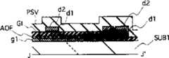
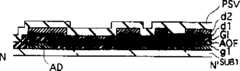
图7是沿图2的线3-3剖开的剖面图,图8是沿图2中的线4-4剖开的薄膜晶体管元件TFT的剖面图,图9是沿图2中的线5-5剖开的存贮电容器Cstg的剖面图。如图7至9所示,相对于液晶层LC,在下透明玻璃基片SUB1的一侧上形成薄膜晶体管TFT、存贮电容器Cstg和一组电极,而在上透明玻璃基片SUB2的一侧上形成滤色器FTL和用于屏蔽光的黑色基质图案BM。Fig. 7 is a sectional view taken along the line 3-3 of Fig. 2, Fig. 8 is a sectional view of the thin film transistor element TFT taken along the line 4-4 in Fig. 2, Fig. 9 is a sectional view taken along the line 5 in Fig. 2 -5 A cross-sectional view of the cutaway storage capacitor Cstg. As shown in Figures 7 to 9, with respect to the liquid crystal layer LC, a thin film transistor TFT, a storage capacitor Cstg and a group of electrodes are formed on one side of the lower transparent glass substrate SUB1, and on one side of the upper transparent glass substrate SUB2 A color filter FTL and a black matrix pattern BM for shielding light are formed.
此外,在透明玻璃基片SUB1和SUB2的内表面(液晶LC的一面)上设置用于控制液晶初始取向的取向膜ORI1和ORI2,并且在透明玻璃基片SUB2和SUB1的外表面设置其极化轴垂直相交的偏振器片(正交尼科耳装置)。In addition, orientation films ORI1 and ORI2 for controlling the initial orientation of liquid crystals are arranged on the inner surfaces of the transparent glass substrates SUB1 and SUB2 (one side of the liquid crystal LC), and the polarization films ORI1 and ORI2 are arranged on the outer surfaces of the transparent glass substrates SUB2 and SUB1. Polarizer sheets with perpendicular axes (crossed Nicols arrangement).
[TFT基片][TFT substrate]
现在详细描述下透明玻璃基片SUB1(TFT基片)的结构。Now, the structure of the transparent glass substrate SUB1 (TFT substrate) will be described in detail.
[薄膜晶体管TFT][Thin Film Transistor TFT]
薄膜晶体管TFT这样操作:当将正偏压加到其栅极GT上时,漏极和源极之间的通道电阻减小;而当零偏压加到其栅极GT上时,通道电阻增加。The thin film transistor TFT operates like this: when a positive bias voltage is applied to its gate GT, the channel resistance between the drain and source decreases; and when a zero bias voltage is applied to its gate GT, the channel resistance increases .
参见图8,薄膜晶体管TFT包括栅极GT、栅极绝缘膜、由本征型非晶硅(a-Si)构成的本征型半导体层AS(没有掺入决定本征导电性类型的杂质)、一对源极SD1和漏极SD2。通常由其间所加偏压的极性来判别源极和漏极。因此,应该注意在工作期间源极和漏极是可以互换的。然而,在下面的描述中,仅为了描述方便,将其中的任一个固定地表示为源极,而另一个则表示为漏极。Referring to FIG. 8, the thin film transistor TFT includes a gate GT, a gate insulating film, an intrinsic type semiconductor layer AS composed of intrinsic type amorphous silicon (a-Si) (without doping impurities that determine the type of intrinsic conductivity), A pair of source SD1 and drain SD2. The source and drain are usually identified by the polarity of the bias voltage applied therebetween. Therefore, it should be noted that the source and drain are interchangeable during operation. However, in the following description, any one of them is fixedly represented as a source and the other is represented as a drain for convenience of description only.
[栅极GT][Gate GT]
栅极GT与栅极信号线GL是连接在一起的,并且由栅极信号线GL的区域的部分形成栅极GT。栅极GT是延伸盖满薄膜晶体管TFT的有源区的一部分,而且这样形成栅极GT可完全覆盖本征型半导体层AS(由下面可以看出)。因此,除了该作用以外,栅极GT还可起到保护本征半导体层AS不受外部光或背部照射光的影响的作用。在本实施例中,栅极GT由单个导电膜g1组成。可用例如溅射形成的铝膜作导电膜g1并且在其上形成铝的阳极氧化膜AOF。The gate GT and the gate signal line GL are connected together, and the gate GT is formed by part of the area of the gate signal line GL. The gate GT is a part extending to cover the active region of the thin film transistor TFT, and the gate GT is formed in such a way that it can completely cover the intrinsic semiconductor layer AS (as can be seen below). Therefore, in addition to this role, the gate GT also plays a role of protecting the intrinsic semiconductor layer AS from external light or back-illuminated light. In this embodiment, the gate GT is composed of a single conductive film g1. An aluminum film formed by, for example, sputtering can be used as the conductive film g1 and an anodic oxidation film AOF of aluminum is formed thereon.
[扫描(栅极)信号线GL][Scan (gate) signal line GL]
由导电膜g1构成扫描(栅极)信号线GL。由与形成栅极GT的导电膜g1的同样的步骤形成构成扫描信号线GL的导电膜g1,并且为一整体结构。通过扫描信号线GL,将栅极电压从外电路馈入栅极GT。也在扫描信号线GL上形成铝的阳极氧化膜AOF。将扫描信号线GL与视频信号线DL相交的部分做得较窄以减小相对视频信号线DL的短路概率,而且将此部分一分为二,以致在已经短路的情况下由激光校正装置能将其分开。The scanning (gate) signal line GL is constituted by the conductive film g1. The conductive film g1 constituting the scanning signal line GL is formed in the same steps as the conductive film g1 of the gate electrode GT, and is a unitary structure. Through the scanning signal line GL, the gate voltage is fed into the gate GT from an external circuit. Anodic oxide films AOF of aluminum are also formed on the scanning signal lines GL. The part where the scanning signal line GL intersects with the video signal line DL is made narrower to reduce the short-circuit probability of the relative video signal line DL, and this part is divided into two, so that in the case of a short circuit, the laser calibration device can separate it.
[对电极CT][counter electrode CT]
用与栅极GT和扫描信号线GL相同层的导电膜g1构成对电极CT。在对电极CT上也形成铝的阳极氧化膜AOF。对电极CT被阳极氧化膜AOF完全覆盖并且即使在对电极CT与视频信号线尽可能接近时也能防止短路。此外,可将它们安排成相交。将对电极电压Vcom加在对电极CT上。在本实施例中,在薄膜晶体管截止时将对电极电压Vcom的电位设定为低于加到视频信号线DL上的最低电位的驱动电压Vdmin和由场穿通电压ΔVs产生的最高电位的驱动电压Vdmax之间的中间电位。在需要将用在视频信号驱动器单元中的集成电路的电源电压几乎减半时,应施加交流电压。The counter electrode CT is formed of the conductive film g1 of the same layer as the gate electrode GT and the scanning signal line GL. An anodized film AOF of aluminum is also formed on the counter electrode CT. The counter electrode CT is completely covered by the anodized film AOF and can prevent a short circuit even when the counter electrode CT is as close as possible to the video signal line. Additionally, they can be arranged to intersect. The counter electrode voltage Vcom is applied to the counter electrode CT. In this embodiment, when the thin film transistor is turned off, the potential of the counter electrode voltage Vcom is set to be lower than the driving voltage Vdmin of the lowest potential applied to the video signal line DL and the driving voltage of the highest potential generated by the field punch-through voltage ΔVs Intermediate potential between Vdmax. When it is necessary to almost halve the power supply voltage of the integrated circuit used in the video signal driver unit, an AC voltage should be applied.
[对电极电压信号线CL][Counter electrode voltage signal line CL]
由导电膜g1构成对电极电压信号线CL。通过与形成栅极GT、扫描信号线GL和对电极CT的导电膜g1相同的步骤形成构成对电极电压信号线CL的导电膜g1,并且作为一个整体结构。通过对电极电压信号线CL,将对电极电压Vcom从外电路加到对电极CT上。也在对电极电压信号线上形成铝的阳极氧化膜AOF。与扫描信号线GL的情况相同,与视频信号线DL相交的部分做得较窄以减小相对视频信号线DL的短路概率,而且将此部分一分为二,以致在已经短路的情况下由激光校正装置能将其分开。The counter electrode voltage signal line CL is constituted by the conductive film g1. The conductive film g1 constituting the counter electrode voltage signal line CL is formed by the same steps as forming the conductive film g1 of the gate electrode GT, the scanning signal line GL, and the counter electrode CT, and is structured as a whole. The counter electrode voltage Vcom is applied to the counter electrode CT from an external circuit through the counter electrode voltage signal line CL. Anodic oxidation film AOF of aluminum is also formed on the counter electrode voltage signal line. As in the case of the scanning signal line GL, the part intersecting the video signal line DL is made narrower to reduce the short-circuit probability of the opposite video signal line DL, and this part is divided into two, so that in the case of already short-circuited by A laser alignment device separates it.
[绝缘膜GI][insulation film GI]
将绝缘膜GI用作为将电场传送到薄膜晶体管TFT的栅极GT和半导体层AS的栅极绝缘膜。在栅极GT和扫描信号线GL上形成栅极绝缘膜GI。用例如由等离子体CVD形成的厚度为1200至2700(在本实施例中约为2400)的氮化硅膜作为栅极绝缘膜。这样形成栅极绝缘膜以致围住整个矩阵单元AR,并且移去周边使外连接端DTM、GTM露出。绝缘膜GI使扫描信号线GL、对电极电压信号线CL和视频信号线DL电绝缘。The insulating film GI is used as a gate insulating film that transmits an electric field to the gate GT of the thin film transistor TFT and the semiconductor layer AS. A gate insulating film GI is formed on the gate electrode GT and the scanning signal line GL. A silicon nitride film formed by, for example, plasma CVD with a thickness of 1200 to 2700 Å (approximately 2400 Å in this embodiment) is used as the gate insulating film. The gate insulating film is thus formed so as to surround the entire matrix unit AR, and the periphery is removed to expose the external connection terminals DTM, GTM. The insulating film GI electrically insulates the scanning signal line GL, the counter voltage signal line CL, and the video signal line DL.
[本征半导体层AS][Intrinsic semiconductor layer AS]
半征半导体层AS由非晶硅制成并具有200至2200A的厚度(本实施例约为2000)。层d0为欧姆接触掺有磷的N(+)型非晶硅半导体层,仅在其下面有本征型半导体层AS并且其上方有导电层d1(d2)的部分留下了层d0。The semiconducting semiconductor layer AS is made of amorphous silicon and has a thickness of 200 to 2200 Å (approximately 2000 Å in this embodiment). Layer d0 is an ohmic-contact phosphorus-doped N(+)-type amorphous silicon semiconductor layer, and only the portion with intrinsic semiconductor layer AS below it and conductive layer d1 (d2) above it leaves layer d0.
也在扫描信号线GL、对电极电压信号线CL和视频信号线DL相交的部分(交叉部分)提供本征型半导体层AS。在相交部分处的本征半导体层AS将减小扫描信号线GL,对电极电压信号线CL和视频信号线DL相交部分处的短路概率。The intrinsic type semiconductor layer AS is also provided at a portion (intersection portion) where the scanning signal line GL, the counter voltage signal line CL, and the video signal line DL intersect. The intrinsic semiconductor layer AS at the intersection portion will reduce the short circuit probability at the intersection portion of the scanning signal line GL, the counter voltage signal line CL and the video signal line DL.
[源极SD1、漏极SD2][Source SD1, Drain SD2]
源极SD1和漏极SD2分别由与N(+)型半导体层d0接触的导电膜d1和在导电膜d1上形成的导电膜d2构成。The source SD1 and the drain SD2 are composed of a conductive film d1 in contact with the N(+) type semiconductor layer d0 and a conductive film d2 formed on the conductive film d1, respectively.
导电膜d1是由通过溅射形成的铬(Cr)膜制成,且厚度为500至1000A(本实施例约为600A)。由于随着Cr膜厚度的增加会产生应力,所以使形成的Cr膜厚度不大于约2000A。使用Cr膜以改善与N(+)型半导体层d0的粘附性并且防止铝导电膜d2不扩散到N(+)型半导体层d0中(即,用作通常所说阻挡层)。除Cr膜以外,还可用高熔点金属(Mo、Ti、Ta或W)的膜以及高熔点的金属硅化物(MoSi2、TiSi2、TaSi2或WSi2)的膜作为导电膜d1。The conductive film d1 is made of a chromium (Cr) film formed by sputtering, and has a thickness of 500 to 1000 Å (approximately 600 Å in this embodiment). Since stress occurs as the thickness of the Cr film increases, the Cr film is formed to have a thickness not greater than about 2000 Å. The Cr film is used to improve adhesion to the N(+) type semiconductor layer d0 and to prevent the aluminum conductive film d2 from diffusing into the N(+) type semiconductor layer d0 (ie, to serve as a so-called barrier layer). In addition to the Cr film, a film of a high melting point metal (Mo, Ti, Ta, or W) and a film of a high melting point metal silicide (MoSi2 , TiSi2 , TaSi2 , or WSi2 ) can be used as the conductive film d1.
由溅射铝(Al)形成厚度为3000至5000的导电膜d2(本实施例约为4000A)。Al膜产生的应力比Cr膜小,所以能形成有较大厚度的Al膜以减小源极SD1、漏极SD2和视频信号线DL的电阻,并且能可靠地延伸盖满由栅极GT和本征半导体层AS引起的台阶(改善台阶覆盖层)。The conductive film d2 is formed by sputtering aluminum (Al) to a thickness of 3000 to 5000 Å (approximately 4000 Å in this embodiment). The stress produced by the Al film is smaller than that of the Cr film, so the Al film with a larger thickness can be formed to reduce the resistance of the source electrode SD1, the drain electrode SD2 and the video signal line DL, and can reliably extend to cover the gate GT and Steps caused by the intrinsic semiconductor layer AS (improved step coverage).
在用同一掩膜图案制作导电膜d1和d2的图案之后,用同一掩膜或用导电膜d1和d2作掩膜除去N(+)型半导体层d0。也就是说,除导电膜d1和d2的部分外,以自对准方式移去在本征半导体层AS上剩下的N(+)型半导体层d0。在这种情况下,由蚀刻除去N(+)型半导体层d0,从而将本征型半导体层AS的表面蚀刻到某种程度,仍能由改变蚀刻时间来控制蚀刻程度。After patterning the conductive films d1 and d2 using the same mask pattern, the N(+) type semiconductor layer d0 is removed using the same mask or using the conductive films d1 and d2 as a mask. That is, the N(+) type semiconductor layer d0 remaining on the intrinsic semiconductor layer AS is removed in a self-aligned manner except for portions of the conductive films d1 and d2. In this case, the surface of the intrinsic type semiconductor layer AS is etched to a certain extent by removing the N(+) type semiconductor layer d0 by etching, and the etching degree can still be controlled by changing the etching time.
[视频信号线DL][Video signal line DL]
用和源极SD1和漏极SD2的一样的层的第一导电膜d1和第二导电膜d2构成视频信号线DL。而且,视频信号线DL与漏极SD2一体形成。The video signal line DL is constituted by the first conductive film d1 and the second conductive film d2 of the same layer as the source SD1 and the drain SD2. Also, the video signal line DL is integrally formed with the drain SD2.
[象素电极PX][Pixel electrode PX]
由与源极SD1和漏极SD2一样的层的第一导电膜d1和第二导电膜d2构成象素电极PX。而且,象素电极PX与源极SD1一体形成。The pixel electrode PX is constituted by the first conductive film d1 and the second conductive film d2 of the same layer as the source electrode SD1 and the drain electrode SD2. Also, the pixel electrode PX is integrally formed with the source electrode SD1.
[存储电容器Cstg][Storage Capacitor Cstg]
使形成的象素电极PX叠在与薄膜晶体管TFT相连端对着的一边上的末端处的对电极电压信号线CL上。通过图9将清楚这一点,这样的叠加构成了一个存储电容器(电容元件)Cstg,象素电极PX作为存储电容器的一个电极PL2,对电极电压信号线CL作为另一个电极PL1。该存储电容器Cstg的介电膜由用作薄膜晶体管TFT的栅极绝缘膜的绝缘膜GT和阳极氧化膜AOF构成。The formed pixel electrode PX is superimposed on the opposite electrode voltage signal line CL at the end on the side opposite to the connection end of the thin film transistor TFT. As will be clear from FIG. 9, such superposition constitutes a storage capacitor (capacitance element) Cstg, the pixel electrode PX serves as one electrode PL2 of the storage capacitor, and the counter electrode voltage signal line CL serves as the other electrode PL1. The dielectric film of this storage capacitor Cstg is composed of an insulating film GT serving as a gate insulating film of a thin film transistor TFT and an anodic oxide film AOF.
如图2所示,当从上观看时,存储电容器Cstg形成在对电极电压信号线CL的导电膜g1的延伸部分上。As shown in FIG. 2, the storage capacitor Cstg is formed on the extended portion of the conductive film g1 of the counter voltage signal line CL when viewed from above.
在这种情况下,位于存储电容器Cstg的绝缘膜GI下方的电极由具有阳极化的表面的铝制成。因而,存储电容器几乎不引起由通常所说的铝金属须引起的缺陷(与上边电极短路)In this case, the electrode located under the insulating film GI of the storage capacitor Cstg is made of aluminum having an anodized surface. Therefore, the storage capacitor hardly causes defects caused by so-called aluminum whiskers (short circuit with the upper electrode)
[保护膜PSV1][protective film PSV1]
在薄膜晶体管TFT上设置保护膜PSV1。制作保护膜PSV1的主要目的是保护薄膜晶体管TFT免受潮湿等,因而保护膜PSV1必须有高的透明度和良好耐湿性。保护膜PSV1由例如等离子体CVD器件形成的氧化硅膜或氮化硅膜构成,并且保护膜PSV1的厚度约为1μm。A protective film PSV1 is provided on the thin film transistor TFT. The main purpose of making the protective film PSV1 is to protect the thin film transistor TFT from moisture etc., so the protective film PSV1 must have high transparency and good moisture resistance. The protection film PSV1 is composed of, for example, a silicon oxide film or a silicon nitride film formed by a plasma CVD device, and the thickness of the protection film PSV1 is about 1 μm.
形成保护膜包围整个矩阵单元AR,并移去其周边部分使外连接端DTM、GTM露出。至于保护膜PSV1和栅极绝缘膜GI的厚度,考虑到保护效果,形成的保护膜有较大厚度,考虑到与晶体管的互导gm,形成具有较小厚度的栅极绝缘膜。因此,呈现好的保护效果的保护膜PSV1做得比栅极绝缘膜GI大,以备即使周边部分尽可能宽也能起保护作用。A protective film is formed to surround the entire matrix unit AR, and its peripheral part is removed to expose the external connection terminals DTM and GTM. As for the thicknesses of the protective film PSV1 and the gate insulating film GI, the protective film is formed with a larger thickness in consideration of the protective effect, and the gate insulating film is formed with a smaller thickness in consideration of the mutual conductance gm with the transistor. Therefore, the protection film PSV1 exhibiting a good protection effect is made larger than the gate insulating film GI in order to provide protection even if the peripheral portion is as wide as possible.
[滤色器基片][Color filter substrate]
现在,再参照图2和图7,详细描述上透明玻璃基片SUB2(波色器基片)的结构。Now, referring again to FIG. 2 and FIG. 7, the structure of the upper transparent glass substrate SUB2 (wave color device substrate) will be described in detail.
[遮光膜BM][Shading film BM]
在上透明玻璃基片SUB2上形成遮光膜BM(通常所说的黑色基质),使不希望通过间隔(除在象素电极PX和对电极CT之间的间隔以外的间隔)透射的光不进入显示表面的一边,从而不使对比度等变坏。遮光膜BM也用于防止外部光或背部照明光射在本征型半导体层AS上。也就是说,薄膜晶体管TFT的本征型半导体层AS夹在遮光膜BM和位于上、下边的大尺寸栅电极GT之间,而且,本征型半导体层AS也不从外边接收自然光或背部照明光。Form light-shielding film BM (commonly referred to as black matrix) on upper transparent glass substrate SUB2, the light that does not wish to transmit through the space (except the space between the pixel electrode PX and the counter electrode CT) does not enter One side of the display surface so as not to deteriorate contrast etc. The light shielding film BM is also used to prevent external light or backlighting light from striking the intrinsic type semiconductor layer AS. That is to say, the intrinsic type semiconductor layer AS of the thin film transistor TFT is sandwiched between the light-shielding film BM and the large-sized gate electrode GT located on the upper and lower sides, and the intrinsic type semiconductor layer AS does not receive natural light or backlight from the outside. Light.
图2所示的遮光膜BM的多边形轮廓线表示其内没有形成遮光膜BM的开口。这仅是轮廓线的一个实例。当希望形成大开口部分时图案可为图3所示的一个。在图3的区域A中,电场的方向不规则并且这一部分的显示按这部分是黑的显示黑色和是白色时显示白色的1对1的方式与象素中的视频数据对应。因而,可利用此部分作为显示的部分。此外,由上、下基片的精确读数确定沿上、下方向的边界。当精确读数超过位于视频信号线DL两边的对电极CT的宽度时,可在对电极的宽度内通过设置边界线来加宽开口部分。The polygonal contour line of the light shielding film BM shown in FIG. 2 indicates an opening in which the light shielding film BM is not formed. This is just one example of a contour line. The pattern may be the one shown in FIG. 3 when it is desired to form a large opening portion. In the area A of FIG. 3, the direction of the electric field is irregular and the display of this part corresponds to the video data in the pixel in a 1-to-1 manner when the part is black and white. Therefore, this part can be used as a displayed part. In addition, boundaries along the upper and lower directions are determined from accurate readings of the upper and lower substrates. When the accurate reading exceeds the width of the counter electrode CT located on both sides of the video signal line DL, the opening portion can be widened by setting a boundary line within the width of the counter electrode.
遮光膜BM对光具有遮光特性,并且由非常绝缘的膜构成,不影响象素电极PX和对电极CT之间的电场。这能使与基片表面平行的电场分量有效地加到液晶层上,并且能减小驱动液晶的电压。遮光膜BM由将黑色颜料混入抗蚀剂所得到的材料制成,BM的厚度约为1.2μm。作为另一实施例,可用将钯和无电镀镍混入抗蚀剂材料中所得到料料制做遮光膜BM。The light-shielding film BM has light-shielding properties against light, and is composed of a very insulating film that does not affect the electric field between the pixel electrode PX and the counter electrode CT. This enables the electric field component parallel to the surface of the substrate to be effectively applied to the liquid crystal layer, and reduces the voltage for driving the liquid crystal. The light-shielding film BM is made of a material obtained by mixing a black pigment into a resist, and the thickness of the BM is about 1.2 μm. As another example, the light-shielding film BM can be made of a material obtained by mixing palladium and electroless nickel into a resist material.
在这种情况下,能在一定程度上增加象素电极PX和对电极CT之间的间隔,从而能增加孔径比。In this case, the interval between the pixel electrode PX and the counter electrode CT can be increased to some extent, so that the aperture ratio can be increased.
将遮光膜BM制成包围象素的晶格状。晶格分开每一象素的有效显示面积。因而,由遮光膜BM清楚地示出了每一象素轮廓。也就是说,遮光膜BM有两个功能,黑色矩阵和屏蔽射到本征型半导体层AS上的光。The light-shielding film BM is made into a lattice shape surrounding pixels. The lattice separates the effective display area of each pixel. Thus, the outline of each pixel is clearly shown by the light-shielding film BM. That is to say, the light-shielding film BM has two functions, black matrix and shielding of light incident on the intrinsic type semiconductor layer AS.
即使在周边部分遮光膜BM也制成格状,而且遮光膜BM的图案与具有多个象点阵一样的开口的矩阵单元的图案邻接。在周边部分上的遮光膜BM向外延伸盖满密封部分SL,以防止漏光例如由安装显示器的装置(此如个人计算机)所反射的光进入矩阵单元。遮光膜BM距基片SUB2的边缘约0.3到1.0mm,而且没有延伸到基片SUB2的切割区域。The light-shielding film BM is made in a lattice shape even in the peripheral portion, and the pattern of the light-shielding film BM is adjacent to the pattern of a matrix unit having a plurality of openings like a dot matrix. The light-shielding film BM on the peripheral portion extends outward to cover the sealing portion SL to prevent leakage of light such as light reflected by a device on which a display is mounted, such as a personal computer, from entering the matrix unit. The light-shielding film BM is about 0.3 to 1.0 mm from the edge of the substrate SUB2, and does not extend to the cutting area of the substrate SUB2.
[滤色器FIL][color filter FIL]
滤色器FIL在面向象素的位置形成循环的红、绿和兰线带。使形成的滤色器FIL叠置在遮光膜BM的边缘部分。The color filter FIL forms a cyclic band of red, green and blue lines at positions facing the pixels. The formed color filter FIL is stacked on the edge portion of the light shielding film BM.
按下面所述形成滤色器FIL。首先,在上透明玻璃基片SUB2的表面上形成可染色部分,例如丙烯酸树脂,接着利用光刻技术除去可染色部分,使可染色部分留在红滤色器形成区上。然后,用红色染料使可染色部分着色并使颜色固着以形成红色滤色器R。接着,用同样的方法依次形成绿色滤色器G和兰色滤色器。The color filter FIL is formed as described below. First, a dyeable portion such as acrylic resin is formed on the surface of the upper transparent glass substrate SUB2, and then the dyeable portion is removed by photolithography so that the dyeable portion remains on the red filter forming region. Then, the dyeable portion is colored with a red dye and the color is fixed to form a red color filter R. Next, a green color filter G and a blue color filter are sequentially formed by the same method.
[涂层膜OC][Coating film OC]
提供涂层膜OC以防止滤色器FIL的染料漏进液晶LC中并且弄平面滤色器FIL和遮光膜BM形成的台阶。由透明树脂材料(例如丙烯酸树脂、环氧树脂或类似的树脂)形成涂层膜OC。The coating film OC is provided to prevent the dye of the color filter FIL from leaking into the liquid crystal LC and to flatten the steps formed by the color filter FIL and the light shielding film BM. The coating film OC is formed of a transparent resin material such as acrylic resin, epoxy resin, or the like.
[液晶层和偏振器板][Liquid crystal layer and polarizer plate]
下面将描述液晶层、取向膜和偏振器板。The liquid crystal layer, alignment film and polarizer plate will be described below.
[液晶层][liquid crystal layer]
使用正介电常数各向异性量Δε为13.2折射率各向异性量Δn为0.081(在20℃时为589nm)的向列液晶,和负介电常数各向异性量Δε为-7.3、折射率各向异性量Δn为0.053(在20℃时为589nm)的向列液晶作为液晶材料LC。当液晶层具有正介电常数各向异性量Δε时其厚度不小于2.8μm并且不大于4.5μm。Use a nematic liquid crystal with a positive dielectric constant anisotropy Δε of 13.2 and a refractive index anisotropy Δn of 0.081 (589 nm at 20°C), and a negative dielectric constant anisotropy Δε of -7.3, refractive index A nematic liquid crystal having an anisotropy amount Δn of 0.053 (589 nm at 20° C.) was used as the liquid crystal material LC. The thickness of the liquid crystal layer is not less than 2.8 μm and not more than 4.5 μm when it has a positive dielectric constant anisotropy amount Δε.
在这种情况下,当光程差Δn.d不小于0.25μm且不大于0.32μm时,可获得在可见光范围内几乎不随波长而变的透射系数,具有正介电常数各向异性量Δε的大多数液晶都具有不小于0.07且不大于0.09的双折射各向异性量Δn。In this case, when the optical path difference Δn.d is not less than 0.25 μm and not more than 0.32 μm, a transmittance that hardly varies with wavelength in the visible range can be obtained, with a positive dielectric constant anisotropy Δε Most liquid crystals have a birefringent anisotropy amount Δn of not less than 0.07 and not more than 0.09.
另一方面,当液晶层具有负介电常数各向异性量Δε时,其厚度(间隔)不小于4.2um且不大于8.0μm。其理由是,必需将光程差Δn.d确定在不小于0.25μm且不大于0.32μm的范围内,与具有正介电常数各向异性量Δε的液晶的情况一样。在这种情况下,具有负介电常数各向异性量Δε的大多数液晶都具有不小于0.04且不大于0.06的双折射各向异性量Δn。On the other hand, when the liquid crystal layer has a negative dielectric constant anisotropy amount Δε, its thickness (interval) is not less than 4.2 µm and not more than 8.0 µm. The reason for this is that it is necessary to determine the optical path difference Δn.d within a range of not less than 0.25 µm and not more than 0.32 µm, as in the case of liquid crystals having a positive dielectric constant anisotropy amount Δε. In this case, most liquid crystals having a negative dielectric constant anisotropy amount Δε have a birefringent anisotropy amount Δn of not less than 0.04 and not more than 0.06.
当液晶分子从磨擦方向RDR向电场方向EDR转动约45°时,下面将叙述的取向膜和偏振器片的组合能获得最大透射系数。When the liquid crystal molecules rotate about 45° from the rubbing direction RDR to the electric field direction EDR, the combination of the alignment film and the polarizer plate described below can obtain the maximum transmission coefficient.
使用聚合物珠粒控制液晶层的厚度(间隔)。The thickness (spacing) of the liquid crystal layer is controlled using polymer beads.
对液晶材料LC没有特殊的限定,只要它是向列液晶材料就可以。驱动电压能随着介电常数各向异性量Δε的增加而减小。液晶层的厚度(间隔)随折射率各向异性量Δn的减小而增加,以致能缩短灌入液晶的时间并减少间隔的变化。The liquid crystal material LC is not particularly limited as long as it is a nematic liquid crystal material. The driving voltage can be decreased as the amount of dielectric constant anisotropy Δε increases. The thickness (interval) of the liquid crystal layer increases as the refractive index anisotropy amount Δn decreases, so that the time for filling the liquid crystal can be shortened and the variation in the interval can be reduced.
[取向膜][Orientation film]
取向膜ORI由聚酰胺制成。上、下基片具有彼此平行的磨擦方向,并且相对于所加电场的方向EDR形成75°的角度。图18表示出它们的相互关系。The orientation film ORI is made of polyamide. The upper and lower substrates have rubbing directions parallel to each other and form an angle of 75° with respect to the direction EDR of the applied electric field. Figure 18 shows their interrelationships.
当液晶材料的介电常数各向异性量Δε为正时,由磨擦方向RDR和所加电场方向EDR形成的角度可以大于45°但小于90°;当液晶材料的介电常数各向异性量Δε为负时,该角度可大于0°但小于45°。When the dielectric constant anisotropy Δε of the liquid crystal material is positive, the angle formed by the rubbing direction RDR and the applied electric field direction EDR can be greater than 45° but less than 90°; when the dielectric constant anisotropy Δε of the liquid crystal material When negative, the angle can be greater than 0° but less than 45°.
[偏振片][Polarizer]
图18表示出所加电场方向、磨擦方向、和偏振片的透光轴之间的相互关系。Fig. 18 shows the correlation among the direction of the applied electric field, the rubbing direction, and the transmission axis of the polarizing plate.
所用的偏振片POL是由Nitto Co.制造的G1220DU,下偏振片POL1的透光轴MAX1大致平行于磨擦方向RDR,并和上偏振片POL2的透光轴MAX2相交成大约90°角。图18表示它们的相互关系。从而获得了常闭特性,使透光系数随加到象素上的电压(在象素电极PX和对电极CT之间的电压)的增加而增加。The polarizer POL used is G1220DU manufactured by Nitto Co., and the transmission axis MAX1 of the lower polarizer POL1 is approximately parallel to the rubbing direction RDR, and intersects the transmission axis MAX2 of the upper polarizer POL2 at an angle of about 90°. Fig. 18 shows their interrelationships. Thus, a normally-off characteristic is obtained, so that the transmittance increases with an increase in the voltage applied to the pixel (the voltage between the pixel electrode PX and the counter electrode CT).
[矩阵周边的组成][Composition around the matrix]
图10是一个平面图,表示包括上、下玻璃基片SUB1和SUB2在内的一个显示板PNL的矩阵(AR)的周边的主要部分。图11是一个剖面图,图11的左侧表示要连接到扫描电路的外部连接端GTM及其附近,图11的右侧表示没有外部连接端的密封部分及其附近。Fig. 10 is a plan view showing a main part of the periphery of a matrix (AR) of a display panel PNL including upper and lower glass substrates SUB1 and SUB2. 11 is a cross-sectional view, the left side of FIG. 11 shows the external connection terminal GTM to be connected to the scanning circuit and its vicinity, and the right side of FIG. 11 shows the sealing portion without the external connection terminal and its vicinity.
当要制作的显示板的尺寸较小时,可在一个玻璃片上制造多个器件,然后再进行分割,以改进生产效率。当显示板尺寸很大时,要制作生产设备通用的标准尺寸的玻璃板,并将其切割成符合该型号的尺寸。不管那种情况,都要在对玻璃进行预定步骤的处理后再进行切割。图10和11表示的正是后一种情况的实例,并且表示出切割后的上、下基片SUB1、SUB2,其中LN代表切割前的两个基片的边缘。在每种情况的成品状态下,上基片SUB2小于下基片SUB1,因此露出了存在外部连接端组Tg和Td以及端子CTM(图中的上侧和左侧)的那些部分。连接端组Tg、Td被指定为多个端:端GTM用于连接扫描电路、端DTM用于连接视频信号电路、以及安装集成电路芯片CHI的带式封装组件TCP(Tape Carrier Package)单元中的引出线。从每一组的矩阵单元向外部连接端单元的引出线向两侧倾斜。其理由是,显示板PNL的连接端DTM、 GTM要符合组件TCP的排列间距和组件TCP中连接端的间距。对电极端CTM用于从外部电路向对电极施加对电极电压。将矩阵单元的对电极信号线CL引出到用于扫描电路的端GTM的相对一侧(图的右侧),并且通过公用总线线CB将对电极电压信号线汇总在一起并连到对电极端CTM。When the size of the display panel to be produced is small, multiple devices can be produced on one glass sheet and then divided to improve production efficiency. When the size of the display panel is large, a glass panel of a standard size common to production equipment is made and cut to a size that fits the model. In either case, cutting is performed after the glass has been subjected to a predetermined step of processing. Figures 10 and 11 show an example of exactly the latter case, and show the upper and lower substrates SUB1, SUB2 after dicing, where LN represents the edges of the two substrates before dicing. In the finished state in each case, the upper substrate SUB2 is smaller than the lower substrate SUB1, thus exposing those parts where the external connection terminal groups Tg and Td and the terminals CTM (upper and left in the figure) exist. The connection terminal groups Tg and Td are designated as multiple terminals: the terminal GTM is used to connect the scanning circuit, the terminal DTM is used to connect the video signal circuit, and the tape package component TCP (Tape Carrier Package) unit for installing the integrated circuit chip CHI pinout. The lead-out lines from the matrix units of each group to the external connection terminal units are inclined to both sides. Its reason is, the connecting terminal DTM, GTM of display panel PNL will accord with the arrangement spacing of component TCP and the spacing of connecting terminal in component TCP. The counter electrode terminal CTM is used to apply a counter electrode voltage to the counter electrode from an external circuit. The opposite electrode signal line CL of the matrix unit is led out to the opposite side of the terminal GTM for the scanning circuit (right side of the figure), and the opposite electrode voltage signal line is brought together and connected to the opposite electrode terminal through the common bus line CB CTM.
在两个透明的玻璃基片SUB1和SUB2之间形成一个密封结构SL,只留下一个液晶填充口INJ,以备灌注液晶LC。该密封材料例如是一种环氧树脂。A sealing structure SL is formed between the two transparent glass substrates SUB1 and SUB2, leaving only one liquid crystal filling port INJ for filling the liquid crystal LC. The sealing material is, for example, an epoxy resin.
在密封结构SL的内部形成取向膜ORI1和ORI2。在透明的下玻璃基片SUB1和透明的上玻璃基片SUB2的外部表面上形成偏振片POL1和POL2。液晶LC密封在由密封结构SL隔开的在确定液晶分子取向的下取向膜ORI1和上取向膜ORI2之间的区域内。下取向膜ORI1是在透明的下玻璃基片SUB1的一侧上的保护膜PSV1上形成的。The alignment films ORI1 and ORI2 are formed inside the sealing structure SL. Polarizing plates POL1 and POL2 are formed on the outer surfaces of the transparent lower glass substrate SUB1 and the transparent upper glass substrate SUB2. The liquid crystal LC is sealed in a region between the lower alignment film ORI1 and the upper alignment film ORI2 that determine the alignment of liquid crystal molecules separated by the sealing structure SL. The lower alignment film ORI1 is formed on the protective film PSV1 on one side of the transparent lower glass substrate SUB1.
在该液晶显示器件中,在透明下玻璃基片SUB1上并在透明上玻璃基片SUB2上单独地叠置各个层,在基片SUB2上形成密封结构SL,将透明下玻璃基片SUB1和透明上玻璃基片SUB2相互叠加在一起,通过在密封件SL上形成的开口INJ注入液晶LC,并用环氧树脂或类似树脂密封填充口INJ。然后切割上、下基片,得到液晶显示器件。In this liquid crystal display device, each layer is stacked separately on the transparent lower glass substrate SUB1 and on the transparent upper glass substrate SUB2, a sealing structure SL is formed on the substrate SUB2, and the transparent lower glass substrate SUB1 and the transparent The upper glass substrates SUB2 are superimposed on each other, the liquid crystal LC is injected through the opening INJ formed in the sealing member SL, and the filling port INJ is sealed with epoxy resin or the like. Then the upper and lower substrates are cut to obtain a liquid crystal display device.
[栅极端单元][Gate terminal unit]
图12A和12B表示从显示矩阵的扫描信号线GL到它的外部连接端GTM的连接结构,其中图12A是平面图,图12B是沿图12A的B-B线剖开的剖面图。为方便说明,只用一根直线代表倾斜的引线。12A and 12B show the connection structure from the scanning signal line GL of the display matrix to its external connection terminal GTM, wherein FIG. 12A is a plan view, and FIG. 12B is a sectional view taken along line B-B of FIG. 12A. For the sake of illustration, only a straight line is used to represent the slanted leads.
符号AO代表直接光刻图形的边界线,或者换句话说,是所选阳极氧化的光刻图案。因此,在阳极氧化后要除掉光刻胶,图中所示的图案AO不留在最终的产品中。但如剖面图所示,在栅极线GL上有选择地形成氧化膜AOF,并膜AOF的痕迹依然保留着。在平面图中,用保护膜覆盖光刻胶的边界线AO的左侧,因此这里不经受阳极氧化作用,线AO的右侧未用保护膜覆盖,因此这里要经受阳极氧化作用。在阳极氧化的铝层g1的表面上形成一个氧化物Al2O3膜AOF,其下侧的导电部分的体积下降了。通过确定适宜的时间和电压来进行阳极氧化,从而即可保留导电部分。The symbol AO represents the boundary line of the direct lithographic pattern, or in other words, the lithographic pattern of the selected anodization. Therefore, the photoresist is removed after anodizing, and the pattern AO shown in the figure does not remain in the final product. However, as shown in the sectional view, the oxide film AOF is selectively formed on the gate line GL, and traces of the film AOF remain. In plan view, the left side of the boundary line AO of the photoresist is covered with a protective film and thus is not subjected to anodization, and the right side of the line AO is not covered with a protective film and is therefore subject to anodization. An oxide Al2 O3 film AOF is formed on the surface of the anodized aluminum layer g1, and the volume of the conductive portion on the lower side thereof is reduced. Anodization is carried out by determining the appropriate time and voltage so that the conductive part remains.
在附图中,为便于理解给铝层g1画上阴影线,但没有阳极氧化的区域画成梳齿形状。其理由是,当铝层宽度很大时,在表面上有金属触须产生。因此,每根线图案形成的很窄,并且将多个线图案平行地聚结在一起,以减小破裂的可能性并减小电导率,同时还能防止金属触须的产生。In the drawings, the aluminum layer g1 is hatched for easy understanding, but the areas not anodized are drawn in a comb shape. The reason for this is that when the width of the aluminum layer is large, metal whiskers are generated on the surface. Therefore, each wire pattern is formed narrow, and a plurality of wire patterns are coalesced together in parallel to reduce the possibility of cracking and reduce electrical conductivity, while also preventing generation of metal whiskers.
栅极端GTM包括铝层g1和透明的导电层g2,导电层g2对该表面进行保护,并改善连接到TCP(带状封装组件)的可靠性。透明的导电膜g2是通过溅射形成的膜(铟锡氧化物ITO:Nesa膜),厚度为1000-2000A(在本实施中约为1400A)。在铝层g1上及其侧面上形成导电层d1和d2,将铬层d1连到铝层和透明导电层g2上,以补偿铝层和透明导电层g2之间的性能很差的连接并减小连接电阻。由于导电层d2是使用和形成导电层d1相同的掩膜形成的,所以导电层d2依然保留。The gate terminal GTM includes an aluminum layer g1 and a transparent conductive layer g2 which protects the surface and improves the reliability of connection to a TCP (Tape Package Module). The transparent conductive film g2 is a film formed by sputtering (indium tin oxide ITO:Nesa film) with a thickness of 1000-2000A (approximately 1400A in this embodiment). Conductive layers d1 and d2 are formed on the aluminum layer g1 and its side faces, and the chromium layer d1 is connected to the aluminum layer and the transparent conductive layer g2 to compensate for the poor connection between the aluminum layer and the transparent conductive layer g2 and reduce the Small connection resistance. Since the conductive layer d2 is formed using the same mask as that used to form the conductive layer d1, the conductive layer d2 remains.
在平面图中,在边界线右侧形成栅极绝缘膜GI,在边界线右侧形成保护膜P.SV1,并且露出设在左侧的端单元GTM使其可与外部电路欧姆接触。附图中只表示出一对栅极线和栅极端。但实际上,在图12A和12B所示的上、下侧设置多对栅极线和栅极端,从而构成一个端组Tg(图10)。在生产过程中,栅极端的左端超过该区域以便对基片进行切割,并且通过引线SHg(未示出)将该左端短路。在生产过程中,这个短路线SHg用于提供阳极氧化期间的电源,并在磨擦取向膜ORI1时用于防止静电击穿。In plan view, the gate insulating film GI is formed on the right side of the boundary line, the protective film P.SV1 is formed on the right side of the boundary line, and the terminal cell GTM provided on the left side is exposed so as to be in ohmic contact with an external circuit. Only a pair of gate lines and gate terminals are shown in the drawings. Actually, however, a plurality of pairs of gate lines and gate terminals are provided on the upper and lower sides shown in FIGS. 12A and 12B, thereby constituting one terminal group Tg (FIG. 10). During the production process, the left end of the gate terminal exceeds this area to cut the substrate, and the left end is short-circuited by a wire SHg (not shown). During production, this short line SHg is used to provide power during anodization and to prevent electrostatic breakdown when rubbing the alignment film ORI1.
[漏极端DTM][Drain terminal DTM]
图13A和13B表示视频信号线DL和外部连接端DTM的连接,其中图13A是平面图,图13B是沿图13A的B-B线的剖面图。这两个附图对应于图19的上部。由于为方便起见改变了附图的方向,其左端的方向对应于基片SUB1的上端。13A and 13B show the connection of the video signal line DL and the external connection terminal DTM, wherein FIG. 13A is a plan view, and FIG. 13B is a sectional view along line B-B of FIG. 13A. These two figures correspond to the upper part of FIG. 19 . Since the direction of the drawing is changed for convenience, the direction of its left end corresponds to the upper end of the substrate SUB1.
符号TSTD代表一个检查端,这里不和任何外部电路连接,但这里被加宽,大于引线宽度,因此能和探针或类似物相接触。类似地,漏极端DTM也加宽了,大于引线的宽度,因此可与外部电路相连。沿上、下方向安排和外部电路相连的漏极端DTM,从而构成一个端组Td(省略了脚标)(如图10所示),漏极端DTM超过了基片SUB1的切割线,并且由一个引线SHg(未示出)完全短路以防止生产过程中的静电击穿。如图13A和13B所示,每隔一个视频信号线DL形成一个检查端TSTd。The symbol TSTD represents a check terminal, which is not connected to any external circuit, but which is widened larger than the width of the lead wire, so that it can be contacted with a probe or the like. Similarly, the drain terminal DTM is also widened, larger than the width of the lead, so it can be connected with external circuits. Arrange the drain terminal DTM connected to the external circuit along the upper and lower directions to form a terminal group Td (subscript omitted) (as shown in Figure 10). The drain terminal DTM exceeds the cutting line of the substrate SUB1, and is formed by a The leads SHg (not shown) are dead shorted to prevent electrostatic breakdown during production. As shown in FIGS. 13A and 13B, every other video signal line DL forms a check terminal TSTd.
漏极连接端DTM是通过单个的透明导电层g2形成的,并且在除去了栅极绝缘膜GI的一个部分与视频信号线DL相连。在栅极绝缘膜GI的端部上形成的半导体层AS用于蚀刻栅极绝缘膜GI成锥形。当然,实际上已除去端DTM上的保护膜PSV,从而可与外部电路进行连接。从矩阵单元向漏极端DTM的引出线使层d1、d2和视频信号线DL层具有相同的高度,视频信号线DL层是在保护膜PSV中构成的并且连接到保护膜PSV中的透明导电膜g2上。其理由是,必须尽可能多的利用保护膜PSV和密封结构SL来保护铝层d2,而铝层d2是易受电解腐蚀的。The drain connection terminal DTM is formed through a single transparent conductive layer g2, and is connected to the video signal line DL at a portion where the gate insulating film GI is removed. The semiconductor layer AS formed on the end portion of the gate insulating film GI is used to etch the gate insulating film GI into a tapered shape. Of course, the protective film PSV on the terminal DTM is actually removed so that connection with an external circuit can be made. The lead-out lines from the matrix unit to the drain terminal DTM make the layers d1, d2 have the same height as the video signal line DL layer, which is a transparent conductive film formed in the protective film PSV and connected to the protective film PSV on g2. The reason for this is that the aluminum layer d2, which is susceptible to electrolytic corrosion, must be protected as much as possible with the protective film PSV and the sealing structure SL.
[对电极端CTM][Opposite terminal CTM]
图14A和14B表示从对电极信号线CL到外部连接端CTM的连接,其中图14A是平面图,图14B是沿图14A的B-B线剖开的剖面图。这些图对应于图19的左上部。14A and 14B show the connection from the counter electrode signal line CL to the external connection terminal CTM, wherein FIG. 14A is a plan view, and FIG. 14B is a sectional view taken along line B-B of FIG. 14A. These figures correspond to the upper left part of FIG. 19 .
通过公用总线线CB把对电极电压信号线CL集中在一起,并将其引向对电极端CTM。在公用总线线CB的结构中,在导电层g1上形成导电层d1和导电层d2。其理由是,可减小公用总线线CB的电阻,有效地把对电极电压从外部电路提供给对电极电压信号线CL。The opposite electrode voltage signal lines CL are collected together through the common bus line CB and lead to the opposite electrode terminal CTM. In the structure of the common bus line CB, the conductive layer d1 and the conductive layer d2 are formed on the conductive layer g1. The reason is that the resistance of the common bus line CB can be reduced, and the counter electrode voltage can be efficiently supplied from the external circuit to the counter electrode voltage signal line CL.
因此,可充分传递对电极电压,甚至可传递到端部象素,因而有可能减小由对电极CT响应于加到视频信号线DL的视频信号产生的电压畸变引起的交叉干扰(尤其是屏幕左-右方向的交叉干扰)的发生。这种结构的特征是,在不另外提供导电层的条件下就能减小公用总线线的电阻。公用总线线CB的导电层g1没有阳极氧化,因此层g1可以电连接到导电层d1和导电层d2。此外,导电层g1通过栅极绝缘膜GI露出。Therefore, the counter electrode voltage can be sufficiently transmitted even to the end pixels, and thus it is possible to reduce the crosstalk caused by the voltage distortion of the counter electrode CT in response to the video signal applied to the video signal line DL (especially the screen Cross-talk in the left-right direction) occurs. This structure is characterized in that the resistance of the common bus line can be reduced without additionally providing a conductive layer. The conductive layer g1 of the common bus line CB is not anodized, so the layer g1 can be electrically connected to the conductive layer d1 and the conductive layer d2. In addition, the conductive layer g1 is exposed through the gate insulating film GI.
在对电极端CTM的结构中,在导电层g1上形成透明的导电层g2。通过透明的导电层g2来保护该表面,并且用具有良好耐用性的透明的导电层g2覆盖导电层g1,以防止电解腐蚀。In the structure of the counter electrode terminal CTM, a transparent conductive layer g2 is formed on the conductive layer g1. The surface is protected by a transparent conductive layer g2 and the conductive layer g1 is covered with a transparent conductive layer g2 with good durability to prevent electrolytic corrosion.
在上述实施例中,在公用总线线CB上形成导电层d1和导电层d2。但本发明决不只限于这些导电层。即使在这种情况下,也有可能减小公用总线线CB的电阻。In the above-described embodiments, the conductive layer d1 and the conductive layer d2 are formed on the common bus line CB. However, the present invention is by no means limited to these conductive layers. Even in this case, it is possible to reduce the resistance of the common bus line CB.
[制造方法][Manufacturing method]
下面参照图15-17描述制造上述液晶显示器件的基片SUB1的方法。在这些图中,中央部分的字符代表步骤名称的缩写,左侧代表图8所示的薄膜晶体管,右侧表示图12A和12B的剖面图所示的栅极端附近的工艺流程。步骤A-I(除步骤B和D以外)都是按光处理分开的。每个步骤的剖面图都代表结束了光处理并且除去光刻胶后的一个阶段。在本实施例中的光处理指的是从使用一个掩模来涂敷光刻到通过所选的曝光量对其显像的一系列操作。现在针对每一个分开的步骤来描述该光处理。Next, a method of manufacturing the substrate SUB1 of the above-mentioned liquid crystal display device will be described with reference to FIGS. 15-17. In these figures, the characters in the central part represent the abbreviations of the step names, the left side represents the thin film transistor shown in FIG. 8 , and the right side represents the process flow near the gate terminal shown in the cross-sectional views of FIGS. 12A and 12B . Steps A-I (except steps B and D) are all separated by light treatment. The cross-sectional view at each step represents a stage after the photoprocessing has been completed and the photoresist has been removed. Photoprocessing in this embodiment refers to a series of operations from coating photolithography using a mask to developing it by a selected exposure amount. The light processing is now described for each separate step.
步骤A、图15:Step A, Figure 15:
通过在由AN635(商标名)制成的透明下玻璃基片SUB1上进行溅射形成厚度为3000A的由Al-Pd、Al-Si、Al-Ta、Al-Ti-Ta、或类似物制成的导电膜g1。在光处理后,通过使用磷酸、硝酸、和冰乙酸的混合酸溶液有选择地蚀刻导电胶g1。于是形成:栅极GT、扫描信号线GL、对电极CT、对电极电压信号线CL、电极PL1、栅极端GTM、公用总线线CB的第一导电层,对电极端CTM的第一导电层、用于连接栅极端GTM的阳极氧化的总线线SHg(未示出)、以及连接到阳极氧化的总线线SHg的阳极氧化垫(未示出)。A layer made of Al-Pd, Al-Si, Al-Ta, Al-Ti-Ta, or the like is formed by sputtering on a transparent lower glass substrate SUB1 made of AN635 (trade name) with a thickness of 3000 Å. The conductive film g1. After the light treatment, the conductive paste g1 was selectively etched by using a mixed acid solution of phosphoric acid, nitric acid, and glacial acetic acid. Thus, the first conductive layer of the gate GT, the scanning signal line GL, the counter electrode CT, the counter electrode voltage signal line CL, the electrode PL1, the gate terminal GTM, the common bus line CB, the first conductive layer of the counter electrode terminal CTM, Anodized bus lines SHg (not shown) for connecting the gate terminal GTM, and anodized pads (not shown) connected to the anodized bus lines SHg.
步骤B、图15:Step B, Figure 15:
在通过直接构图法形成阳极氧化掩模AO之后,将基片SUB1浸渍在一种阳极氧化溶液中,该阳极氧化溶液是通过用乙二醇溶液将包含用氨将pH值调节到6.25±0.05的3%的洒石酸稀释到1∶9而获得的,其中将阳极氧化电流密度调节到0.5mA/cm2(恒定电流的阳极氧化)。在阳极氧化电压达到125伏之前一直要进行阳极氧化,这个电压是获得具有预定厚度的Al2O3膜所必需的。最好将这一状态保持几十分钟(恒定电压的阳极氧化)。这从形成均匀的Al2O3膜的观点看是非常重要的。于是,对导电膜g1实现了阳极氧化,并且在栅极GT、扫描信号线GL、对电极CT、对电极电压信号线CL、和电极PL1上形成了厚度为1800A的阳极氧化膜AOF。After forming the anodization mask AO by the direct patterning method, the substrate SUB1 was dipped in an anodization solution prepared by using an ethylene glycol solution containing ammonia to adjust the pH to 6.25±0.05. 3% tartaric acid diluted to 1:9, wherein the anodizing current density was adjusted to 0.5 mA/cm2 (constant current anodizing). Anodization was carried out until the anodization voltage reached 125 V, which is necessary to obtainanAl2O3 film with a predetermined thickness. It is best to keep this state for tens of minutes (constant voltage anodization). This is very important from the viewpoint of forming a uniform Al2 O3 film. Thus, anodization is performed on the conductive film g1, and an anodized film AOF having a thickness of 1800 Å is formed on the gate electrode GT, the scanning signal line GL, the counter electrode CT, the counter voltage signal line CL, and the electrode PL1.
步骤C、图15:Step C, Figure 15:
通过溅射形成厚度为1400的ITO膜的透明导电膜g2、在光处理后,用盐酸和硝酸的混合酸溶液作为蚀刻溶液蚀刻透明导电膜g2,从而形成栅极端GTM的最上层、和漏极端DTM及对电极端CTM的第二导电层。A transparent conductive film g2 of an ITO film having a thickness of 1400 Å is formed by sputtering. After the light treatment, the transparent conductive film g2 is etched with a mixed acid solution of hydrochloric acid and nitric acid as an etching solution, thereby forming the uppermost layer of the gate terminal GTM, and the drain. The second conductive layer of the extreme DTM and the opposite terminal CTM.
步骤D、图16:Step D, Figure 16:
将氨气、硅烷气、和氮气引入一个等离子CVD设备,形成厚度为2200的氮化硅膜。然后,将硅烷气和氢气引入该等离子CVD设备,形成厚度为2000的i型非晶的硅膜。在此之后,将氢气和磷化氢气引入该等离子CVD设备,形成厚度为300的N(+)型非晶的硅膜。Ammonia gas, silane gas, and nitrogen gas were introduced into a plasma CVD apparatus to form a silicon nitride film with a thickness of 2200 Å. Then, silane gas and hydrogen gas were introduced into the plasma CVD apparatus to form an i-type amorphous silicon film with a thickness of 2000 Å. After that, hydrogen gas and phosphine gas were introduced into the plasma CVD apparatus to form an N(+) type amorphous silicon film with a thickness of 300 Å.
步骤E、图16:Step E, Figure 16:
在光处理后,通过使用SF6和CCl4作为干性蚀刻气体,有选择地蚀刻N(+)型非晶硅膜和i型非晶硅膜,从而形成i型半导体层AS的岛状区。After the light treatment, by using SF6 and CCl4 as dry etching gas, the N(+) type amorphous silicon film and the i-type amorphous silicon film are selectively etched, thereby forming island-shaped regions of the i-type semiconductor layer AS .
步骤F,图16:Step F, Figure 16:
在光处理后,通过使用SF6作为干性蚀刻气体有选择地蚀刻氮化硅膜。After the light treatment, the silicon nitride film was selectively etched by using SF6 as a dry etching gas.
步骤G、图17:Step G, Figure 17:
通过溅射形成厚度为600A的由铬构成的导电膜d1,并且通过溅射形成厚度4000A的由Al-Pd、Al-Si、Al-Ta、Al-Ti-Ta、或类似物构成的导电膜d2。在光处理后,使用和步骤A中所用的相同的溶液蚀刻导电膜d2,并且使用高铈硝酸铵溶液蚀刻导电膜d1,从而形成:视频信号线DL、源极SD1、漏极SD2、象素电极PX、电极PL2、公用总线线CB的第二和第三导电层、以及用于短路漏极端DTM的总线线SHd(未示出)。接着,将CCl4和SF6气体引入该干性蚀刻设备,以蚀刻N(+)型非晶硅膜,并且因此可有选择地在源极和漏极之间除去N(+)型半导体层d0。A conductive film d1 composed of chromium to a thickness of 600A was formed by sputtering, and a conductive film composed of Al-Pd, Al-Si, Al-Ta, Al-Ti-Ta, or the like was formed to a thickness of 4000A by sputtering d2. After the light treatment, the conductive film d2 is etched using the same solution as used in step A, and the conductive film d1 is etched using a ceric ammonium nitrate solution, thereby forming: a video signal line DL, a source electrode SD1, a drain electrode SD2, a pixel The electrode PX, the electrode PL2, the second and third conductive layers of the common bus line CB, and the bus line SHd (not shown) for short-circuiting the drain terminal DTM. Next,CCl4 andSF6 gases are introduced into this dry etching equipment to etch the N(+) type amorphous silicon film, and thus the N(+) type semiconductor layer can be selectively removed between the source and drain electrodes d0.
步骤H、图17:Step H, Figure 17:
将氨气、硅烷气、和氮气引入等离CVD设备,以提供厚度为1μm的氮化硅膜。在光处理后,使用SF6作为干性蚀刻气体,通过光刻技术有选择地蚀刻氮化硅膜,以形成保护膜PSV。Ammonia gas, silane gas, and nitrogen gas were introduced into the plasma CVD apparatus to provide a silicon nitride film with a thickness of 1 μm. After the light treatment, the silicon nitride film was selectively etched by photolithography using SF6 as a dry etching gas to form the protective film PSV.
[整个显示器件的等效电路][Equivalent circuit of the entire display device]
图19是显示矩阵单元及其外围电路的等效电路的连接图。该电路图是对应于实际的排列布局位置画出的,其中AR代表一个矩阵阵列,其中的多个象素安排成两维的结构形式。Fig. 19 is a connection diagram showing an equivalent circuit of a matrix unit and its peripheral circuits. The circuit diagram is drawn corresponding to the actual arrangement and layout position, wherein AR represents a matrix array in which a plurality of pixels are arranged in a two-dimensional structure.
在附图中,符号X代表视频信号线DL,并且分别给绿、兰、红象素加上脚标G、B、R。符号Y代表扫描信号线GL,并按扫描定时顺序加上脚标1、2、3、……。In the drawings, a symbol X represents a video signal line DL, and subscripts G, B, R are added to green, blue, and red pixels, respectively. The symbol Y represents the scanning signal line GL, and
将扫描信号线Y(省略了脚标)连接到一个垂直扫描电路V,并将视频信号线X(省略了脚标)连接到视频信号驱动器单元H。A scanning signal line Y (subscript omitted) is connected to a vertical scanning circuit V, and a video signal line X (subscript omitted) is connected to a video signal driver unit H.
SUB代表一个电路,该电路包括一个电源电路,用于产生多种电压,这些电压是通过对一个电压源的电压进行分压而产生的并且这些电压是经过稳压的;该电路还包括一个变换电路,用于把来自一个主机(高阶算术单元)的用于CRT(阴极射线管)的信息转换成用于TFT液晶显示器件的信息。SUB represents a circuit that includes a power supply circuit for generating various voltages that are generated by dividing the voltage of a voltage source and that are regulated; the circuit also includes a transform Circuits for converting information for a CRT (cathode ray tube) from a host computer (higher order arithmetic unit) into information for a TFT liquid crystal display device.
[驱动电路][Drive circuit]
图20表示驱动本发明的液晶显示器件的波形。对电极电压的波形是交变的矩形,有两个值,即Vch和Vcl。为了与其同步,要将扫描信号Vg(i-1)和Vg(i)的非选择电压变为两个值,即,对每个扫描周期为Vglh和Vgll。要将对电极电压的幅度调节到等于该非选择电压的幅度。视频信号电压值是从加到液晶层上的电压减去对电极电压幅度的一半的余数。Fig. 20 shows waveforms for driving the liquid crystal display device of the present invention. The waveform of the counter electrode voltage is an alternating rectangle with two values, Vch and Vcl. To synchronize it, the non-selection voltages of the scan signals Vg(i−1) and Vg(i) are changed to two values, ie, Vglh and Vgll for each scan period. The magnitude of the counter electrode voltage is adjusted to be equal to the magnitude of the non-selection voltage. The video signal voltage value is the remainder obtained by subtracting half of the amplitude of the counter electrode voltage from the voltage applied to the liquid crystal layer.
对电极电压可以是直流电压。但通过使用一个交变电压有可能降低视频信号电压的最大电压,因此有可能使用击穿电压已被减小的视频信号驱动器单元(信号一侧的驱动器)。The counter electrode voltage may be a DC voltage. But it is possible to lower the maximum voltage of the video signal voltage by using an alternating voltage, so it is possible to use a video signal driver unit (driver on the signal side) whose breakdown voltage has been reduced.
[存贮电容器Cstg的操作][Operation of Storage Capacitor Cstg]
提供存贮电容器Cstg把写入一个象素(薄膜晶体管TFT截止以后)的视频数据存贮更长的时间。按照平行于本发明所用的基片的表面施加电场的系统(该系统和垂直于基片的表面施加电场的系统不同),几乎不存在由象素电极和对电极产生的电容(即,所谓液晶电容)。也就是说,液晶电容不可能存贮象素中的视频数据。因此,在平行于基片表面施加电场的系统中,存贮电容Cstg是一个主要的组成元件。The storage capacitor Cstg is provided to store video data written in one pixel (after the thin film transistor TFT is turned off) for a longer period of time. According to the system of applying an electric field parallel to the surface of the substrate used in the present invention (this system is different from the system of applying an electric field perpendicular to the surface of the substrate), there is almost no capacitance generated by the pixel electrode and the counter electrode (that is, the so-called liquid crystal capacitance). In other words, it is impossible for liquid crystal capacitors to store video data in pixels. Therefore, in a system in which an electric field is applied parallel to the substrate surface, the storage capacitor Cstg is a major constituent element.
此外,当薄膜晶体管TFT经受开关操作时,存贮电容器Cstg的作用是降低栅极电位的变化ΔVg对象素电极电位Vs的影响效果。这种情况可由下述公式表示:In addition, the storage capacitor Cstg functions to reduce the effect of the variation ΔVg of the gate potential on the pixel electrode potential Vs when the thin film transistor TFT is subjected to a switching operation. This situation can be represented by the following formula:
ΔVs={Cgs/(Cgs+Cstg+CpiX)}×ΔVg其中:Cgs是薄膜晶体管的栅极GT和源极SD1之间形成的寄生电容,CpiX是象素电极PX和对电极CT之间形成的电容,ΔVS是由ΔVg引起的象素电极电位的变化(即,是一个馈通电压)。这一变化ΔVs是加到液晶LC的直流分量的一个来源,但ΔVs随存贮电容Cstg容量的增加而减小。加到液晶LC的直流分量的减小将使液晶LC的寿命延长,并且将减小所谓的印制图像(即,当液晶显示屏上的画面变化时,前一个画面依然存在)。ΔVs={Cgs/(Cgs+Cstg+CpiX)}×ΔVg wherein: Cgs is the parasitic capacitance formed between the gate GT and the source electrode SD1 of the thin film transistor, and CpiX is the parasitic capacitance formed between the pixel electrode PX and the counter electrode CT The capacitance, ΔVS, is the change in potential of the pixel electrode caused by ΔVg (ie, is a feedthrough voltage). This change ΔVs is a source of the DC component applied to the liquid crystal LC, but ΔVs decreases as the capacity of the storage capacitor Cstg increases. The reduction of the DC component applied to the liquid crystal LC will extend the life of the liquid crystal LC, and will reduce the so-called printed image (ie, when the picture on the liquid crystal display changes, the previous picture remains).
如早些时候曾描述过的,由于增大栅极GT的尺寸可完全覆盖i型半导体层AS,因此也增大了栅极GT和源极SD1彼此重叠的区域,从而加大了寄生电容Cgs,产生了象素电极电位Vs很容易受栅极(扫描)信号Vg影响的不利效果。但设置存贮电容器Cstg消除了这一缺点。As described earlier, since increasing the size of the gate GT can completely cover the i-type semiconductor layer AS, the area where the gate GT and the source SD1 overlap each other is also increased, thereby increasing the parasitic capacitance Cgs , there is an adverse effect that the pixel electrode potential Vs is easily affected by the gate (scanning) signal Vg. But providing the storage capacitor Cstg eliminates this disadvantage.
[将对电极电压信号线CL连接到公用总线线CB的方法][Method of connecting the counter electrode voltage signal line CL to the common bus line CB]
图27是示意表示按本发明第三实施例的液晶显示器件的组成的一个方块图。Fig. 27 is a block diagram schematically showing the composition of a liquid crystal display device according to a third embodiment of the present invention.
本实施例的液晶显示器件包括:其中的象素120以矩阵形式排列的一个矩阵基片SUB1、一个对基片SUB2、一个定时控制器100、一个漏极驱动器单元102、一个栅极驱动器单元104、一个公用电压产生器和驱动器单元103、以及密封在矩阵基片SUB1和对基片SUB2之间的液晶(未示出)。The liquid crystal display device of the present embodiment comprises: a matrix substrate SUB1 wherein the
在矩阵基片SUB1上设有视频信号线DL,用于提供驱动象素120和扫描电路GL所必须的驱动电压。视频信号线DL和扫描信号线GL彼此垂直并且包围象素120,视频信号线DL连到漏极驱动器单元102,扫描信号线连到栅极驱动器单元104。A video signal line DL is provided on the matrix substrate SUB1 for supplying driving voltage necessary for driving the
将在象素120中连到对电极CT的对电极电压信号线CL按排成平行于扫描信号线GL。对电极电压信号线CL在其两端进一步通过公用总线线CB连到公用电压产生器和驱动器单元103。The counter electrode voltage signal line CL connected to the counter electrode CT in the
栅极驱动器单元104和漏极驱动器单元102都连接到定时控制器100。定时控制器100从外部主机101接收视频信号和定时信号,漏极驱动器单元102产生和视频信号对应的驱动电压,并响应于定时信号将其加到视频信号线DL。Both the
栅极驱动器单元104接收来自定时控制器100的定时信号,产生与视频信号对应的栅极驱动电压,并且响应于定时信号将其加到扫描信号线GL。The
结果,使对应于视频信号的漏极电压依次相继地加到矩阵基片SUB1中的象素120上。As a result, drain voltages corresponding to video signals are sequentially applied to the
在该实施例中,对电极电压信号线CL在其两端连到公用总线线CB。这里,公用总线线CB是在矩阵基片的非显示区上形成的,并且使线CB有较大的宽度。因此,可使公用总线线CB的电阻小于对电极电压信号线CL的电阻。In this embodiment, the counter electrode voltage signal line CL is connected at both ends thereof to the common bus line CB. Here, the common bus line CB is formed on the non-display area of the matrix substrate, and the line CB is made to have a larger width. Therefore, the resistance of the common bus line CB can be made smaller than the resistance of the counter electrode voltage signal line CL.
图28表示的是用于传递加到本实施例的液晶显示器中的对电极CT的驱动电压的通路的一个等效电路,图29表示图28相应点的驱动电压的波形。FIG. 28 shows an equivalent circuit of a path for transmitting the drive voltage applied to the counter electrode CT in the liquid crystal display of this embodiment, and FIG. 29 shows the waveform of the drive voltage at the corresponding point in FIG. 28 .
由于公用总线线CB的电阻59小于对电极电压信号线CL的电阻58,所以从公用电压驱动器单元60加到图28中的点D、E、F、和G的驱动电压的波形分别变为如图29所示的D点的对电极电压62、E点的对电极电压63、F点的对电极电压64、以及G点的对电极电压65。Since the
从图29可以看出,本实施例有可能减小从公用电压产生器和驱动器单元103的公用电压驱动器单元60加到对电极CT驱动电压的波形的畸变。As can be seen from FIG. 29, the present embodiment makes it possible to reduce the distortion of the waveform applied from the common
因此,在象素电极PX和对电极CT之间的电场强度在象素120中几乎变为均匀一致,因此有可能减小亮度沿对电极电压信号线CL的变化。Therefore, the electric field intensity between the pixel electrode PX and the counter electrode CT becomes almost uniform in the
即使对电极电压信号线CL发生部分损坏,驱动电压也能从对电极电压信号线的两端提供给对电极CT,从而防止了显示质量受损,这与不再给破损部分后面的象素120的对电极提供驱动电压时并且液晶不再被驱动时的已有技术不同。Even if the counter electrode voltage signal line CL is partially damaged, the driving voltage can be supplied to the counter electrode CT from both ends of the counter electrode voltage signal line, thereby preventing the display quality from being damaged, which is different from no longer supplying to the
图30A是表示在图27的矩阵基片的点A处对电极电压信号线CL和公用总线线CB的连接情况的平面图。图30B是沿图30A的I-I线剖开的剖面图,图30C是沿图30A的H-H线剖开的剖面图。30A is a plan view showing the state of connection of the counter-electrode voltage signal line CL and the common bus line CB at point A of the matrix substrate of FIG. 27. FIG. Fig. 30B is a sectional view taken along line I-I of Fig. 30A, and Fig. 30C is a sectional view taken along line H-H of Fig. 30A.
在图27所示的点A,通过使用铝层g1在矩阵基片上形成扫描信号线GL和对电极电压信号线CL,并对其进行阳极氧化以便在该信号线上形成氧化铝AOF。在这种情况下通过使用一个保护膜,期望在对电极电压信号线CL的端部不要形成氧化铝AOF。接着,形成栅极氧化膜GI。这时,在对电极电压信号线CL的端部形成一个接触孔CHL。然后,通过使用铬层d1和铝层d2,同时形成视频信号线DL和公用总线线CB。即使在对电极电压信号线CL的端部也要形成公用总线线CB,并且通过在对电极电压信号线CL的端部的接触孔CHL将公用总线线CB和对电极电压信号线CL电连接在一起。最后形成保护膜PSV,而后进行表面处理。At point A shown in FIG. 27, scanning signal lines GL and counter electrode voltage signal lines CL are formed on the matrix substrate by using an aluminum layer g1, and anodized to form aluminum oxide AOF on the signal lines. By using a protective film in this case, it is desirable not to form the aluminum oxide AOF at the end of the counter electrode voltage signal line CL. Next, a gate oxide film GI is formed. At this time, a contact hole CHL is formed at the end of the counter electrode voltage signal line CL. Then, by using the chrome layer d1 and the aluminum layer d2, the video signal line DL and the common bus line CB are simultaneously formed. The common bus line CB is formed even at the end of the counter voltage signal line CL, and the common bus line CB and the counter voltage signal line CL are electrically connected through the contact hole CHL at the end of the counter voltage signal line CL. Together. Finally, a protective film PSV is formed, followed by surface treatment.
图31A是表示在图27A的矩阵基片的点B的对电极电压信号线CL和公用总线线CB的连接情况的一个平面图,图31B是沿图31A的J-J线剖开的剖面图。31A is a plan view showing the connection of the counter electrode voltage signal line CL and the common bus line CB at point B of the matrix substrate of FIG. 27A, and FIG. 31B is a cross-sectional view taken along line J-J of FIG. 31A.
通过使用铝层g1在矩阵基片上形成扫描信号线GL,对电极电压信号线CL、和公用总线线CB,并对它们进行阳极氧化,从而在这些信号线上形成氧化铝AOF。进而,在氧化铝AOF上又形成栅极氧化膜GI。在这种情况下通过使用一个保护膜,期望在对电极电压信号线CL的端部以及公用总线线CB上不要形成氧化铝AOF和栅极氧化膜GI。接着,通过使用两层(即,铬层d1和铝层d2,形成视频信号线DL。与此同时,即使在公用总线线CB上也形成铬层d1和铝层d2。于是,铝层g1、铬层d1、和铝层d2就构成了公用总线线CB,线CB具有很小的电阻。最后,形成保护膜PSV,然后对其进行表面处理。Aluminum oxide AOF is formed on these signal lines by forming scanning signal lines GL, counter electrode voltage signal lines CL, and common bus lines CB on a matrix substrate by using an aluminum layer g1 and anodizing them. Furthermore, a gate oxide film GI is formed on the aluminum oxide AOF. By using one protective film in this case, it is desirable not to form the aluminum oxide AOF and the gate oxide film GI on the end of the counter electrode voltage signal line CL and the common bus line CB. Next, by using two layers, namely, the chromium layer d1 and the aluminum layer d2, the video signal line DL is formed. At the same time, the chromium layer d1 and the aluminum layer d2 are formed even on the common bus line CB. Then, the aluminum layer g1, The chromium layer d1 and the aluminum layer d2 constitute the common bus line CB, and the line CB has a small resistance. Finally, a protective film PSV is formed and then subjected to surface treatment.
图32A是表示图27的矩阵基片8上的点C的视频信号线DL和公用总线线CB的交叉情况的平面图,图32B是沿图32A的K-K′线剖开的剖面图。通过使用铝层g1,在矩阵基片上形成扫描信号线GL和对电极电压信号线CL,并对它们进行阳极氧化,从而在这些信号线上形成氧化铝AOF。32A is a plan view showing the intersection of the video signal line DL and the common bus line CB at point C on the matrix substrate 8 of FIG. 27, and FIG. 32B is a cross-sectional view taken along line K-K' of FIG. 32A. By using the aluminum layer g1, the scanning signal lines GL and the counter voltage signal lines CL are formed on the matrix substrate and anodized to form aluminum oxide AOF on these signal lines.
然后,形成栅极氧化膜GI,并且通过使用两个层(即,铬层d1和铝层d2)形成视频信号线DL。最后,形成保护膜PSV,并对其进行表面处理。Then, a gate oxide film GI is formed, and a video signal line DL is formed by using two layers, ie, a chromium layer d1 and an aluminum layer d2. Finally, a protective film PSV is formed and surface treated.
在图30A-30C中,在公用总线线CB和视频信号线DL之间的区域形成对电极电压信号线CL和公用总线线CB之间的连接部分(接触孔CHL)。但不限于此,接触孔CHL还可以在相对于如图33A-33C所示的公用总线线CB来说的和视频信号线DL相对的那一侧上的一些区域中形成。In FIGS. 30A-30C, a connection portion (contact hole CHL) between the counter voltage signal line CL and the common bus line CB is formed in a region between the common bus line CB and the video signal line DL. But not limited thereto, the contact holes CHL may also be formed in some areas on the side opposite to the video signal line DL with respect to the common bus line CB as shown in FIGS. 33A-33C.
图33A是表示在图27的矩阵基片的点A处的对电极电压信号线CL和公用总线线CB的连接情况的另一个实例的平面图,图33B是沿图33A的图Q-Q1线剖开的剖面图,图33C是沿图33A的R-R1线剖开的剖面图。Fig. 33A is a plan view showing another example of the connection situation of the opposite electrode voltage signal line CL and the common bus line CB at the point A place of the matrix substrate of Fig. 27, and Fig. 33B is cut along the QQ1 line of Fig. 33A Figure 33C is a cross-sectional view taken along line RR1 in Figure 33A.
在图27的点A,使用铝层g1在矩阵基片上形成扫描信号线GL和对电极电压信号线CL,并对它们进行阳极氧化,从而在这些线上形成氧化铝AOF。在这种情况下通过使用一个保护膜,期望在对电极电压信号线CL的端部不要形成氧化铝AOF。接着,形成栅极氧化膜GI。这时,在对电极电压信号线CL的端部形成接触孔CHL。接下去,通过使用两个层,即铬层d1和铝层d2,同时形成视频信号线DL和公用总线线CB。At point A of FIG. 27, the scanning signal lines GL and the counter voltage signal lines CL are formed on the matrix substrate using the aluminum layer g1 and anodized to form aluminum oxide AOF on these lines. By using a protective film in this case, it is desirable not to form the aluminum oxide AOF at the end of the counter electrode voltage signal line CL. Next, a gate oxide film GI is formed. At this time, the contact hole CHL is formed at the end of the counter electrode voltage signal line CL. Next, the video signal line DL and the common bus line CB are simultaneously formed by using two layers, ie, the chrome layer d1 and the aluminum layer d2.
即使在对电极电压信号线CL的端部也要形成公用总线线CB,并且通过在对电极电压信号线CL的端部形成的接触孔CHL将公用总线线CB和对电极电压信号线CL电连接在一起。最后,形成保护膜PSV,然后对其进行表面处理。The common bus line CB is formed even at the end of the counter voltage signal line CL, and the common bus line CB and the counter voltage signal line CL are electrically connected through the contact hole CHL formed at the end of the counter voltage signal line CL. together. Finally, a protective film PSV is formed and then surface treated.
在图33A-33C所示的实施例中,在对电极电压信号线CL与公用总线线CB交叉的那些部分上形成氧化铝AOF。In the embodiment shown in FIGS. 33A-33C, aluminum oxide AOF is formed on those portions where the counter voltage signal line CL crosses the common bus line CB.
此外,一般而言,即使在扫描信号线GL上也要形成氧化铝AOF,因此即使在扫描信号线GL和栅极驱动器单元相连的那些部分中也必须形成接触孔CHL。In addition, in general, aluminum oxide AOF is formed even on the scanning signal line GL, and thus the contact hole CHL must be formed even in those portions where the scanning signal line GL and the gate driver unit are connected.
此外,通过使用保护膜,期望在形成接触孔CHL的那些部分上不要形成氧化铝AOF。Furthermore, by using the protective film, it is desirable not to form aluminum oxide AOF on those portions where the contact hole CHL is formed.
在图30A-30C所示的实施例中,在这种情况下,必须准确地形成用于构成接触孔CHL的保护膜,通过接触孔CHL可将对电极电压信号线CL和公用总线线CB连接在一起。In the embodiment shown in FIGS. 30A-30C , in this case, it is necessary to accurately form a protective film for constituting the contact hole CHL through which the counter electrode voltage signal line CL and the common bus line CB can be connected. together.
但在图33的实施例中,保护膜是在相对于公用总线线CB来说和视频信号线DL相对的那一侧上的矩阵基片周边上形成的,从而可形成连接对电极电压信号线CL和公用总线线CB的接触孔CHL以及连接扫描信号线GL和栅极驱动器单元104的接触孔CHL。此外,当对保护膜直接制图时,可放宽精度要求。But in the embodiment of Fig. 33, protective film is formed on the matrix substrate periphery on the opposite side with video signal line DL with respect to common bus line CB, thereby can form connection opposite electrode voltage signal line CL and the contact hole CHL of the common bus line CB and the contact hole CHL connecting the scanning signal line GL and the
如以上所述,公用总线线CB是使用和扫描信号线GL及视频信号线DL相同的材料以及相同的生产步骤沿显示板的边缘形成的。公用总线线CB进一步还连接到对电极电压信号线的两个端部。As described above, the common bus line CB is formed along the edge of the display panel using the same material and the same production steps as the scanning signal line GL and the video signal line DL. The common bus line CB is further connected to both ends of the counter electrode voltage signal line.
图34和35表示该实施例的公用总线线CB的另一种布局。34 and 35 show another layout of the common bus line CB of this embodiment.
公用总线线CB不必沿图27所示的显示板的所有边缘伸展。如图34所示,公用总线线CB可以避开视频信号线DL与漏极驱动器单元102相连的区域。The common bus line CB does not necessarily extend along all the edges of the display panel shown in FIG. 27 . As shown in FIG. 34 , the common bus line CB can avoid the area where the video signal line DL is connected to the
这样作有可能减小在视频信号线DL和公用总线线CB交叉的那些部分产生的寄生电容。Doing so makes it possible to reduce the parasitic capacitance generated at those portions where the video signal line DL and the common bus line CB intersect.
此外,如图35所示,可将公用总线CB分成多个公用总线线CBA、CBB,它们从显示板伸出并且在位于周边的驱动器单元中连接在一起。这有可能减小显示板内部的公用总线线CB的长度。In addition, as shown in FIG. 35, the common bus CB may be divided into a plurality of common bus lines CBA, CBB that protrude from the display panel and are connected together in driver units located at the periphery. This makes it possible to reduce the length of the common bus line CB inside the display panel.
[厚度调节膜AD][Thickness adjustment film AD]
下面描述使用厚度调节膜AD作为组成元件的第四实施例的液晶显示器件。The liquid crystal display device of the fourth embodiment using the thickness adjustment film AD as a constituent element is described below.
图36A是在和图27的矩阵基片上的点A对应的一个点处的对电极电压信号线CL与第三实施例的液晶显示器件中的公用总线线CB相连的一个部分的平面图。图36B是沿图36A的M-M′线剖开的剖面图,图36C是沿图36A的N-N′线剖开的剖面图。36A is a plan view of a portion where the counter electrode voltage signal line CL is connected to the common bus line CB in the liquid crystal display device of the third embodiment at a point corresponding to point A on the matrix substrate of FIG. 27. 36B is a cross-sectional view taken along the line M-M' of FIG. 36A, and FIG. 36C is a cross-sectional view taken along the line N-N' of FIG. 36A.
如图36A所示,在和图27的点A对应的一个点上,使用铝层g1在矩阵基片上形成扫描信号线GL和对电极电压信号线CL,与此同时还形成一个厚度调节膜AD。至少围绕扫描信号线GL形成岛状的厚度调节膜AD,但厚度调节膜AD和扫描信号线GL不要电连接。然后,通过使用和视频信号线DL相同的材料形成公用总线线CB,使其至少在厚度调节膜AD上通过。As shown in FIG. 36A, at a point corresponding to point A in FIG. 27, the scanning signal line GL and the counter electrode voltage signal line CL are formed on the matrix substrate using the aluminum layer g1, and a thickness adjustment film AD is also formed at the same time. . The island-shaped thickness adjustment film AD is formed around at least the scanning signal line GL, but the thickness adjustment film AD and the scanning signal line GL are not electrically connected. Then, the common bus line CB is formed by using the same material as the video signal line DL so as to pass at least on the thickness adjustment film AD.
图37A是表示在第四实施例的液晶显示器件中和图27的矩阵基片上的点B对应的一个点处的对电极电压信号线CL和公用总线线CB的连接情况的平面图,图37B是沿图37A的O-O′线剖开的剖面图。如图37A所示,在和图27的点B相对应的一个点外,通过使用铝层g1在矩阵基片上同时形成扫描信号线GL,对电极电压信号线CL、和公用总线线CB,然后通过栅极氧化膜AOF形成视频信号线DL和厚度调节膜AD。厚度调节膜AD是在公用总线线CB上形成的。37A is a plan view showing the connection of the counter electrode voltage signal line CL and the common bus line CB at a point corresponding to point B on the matrix substrate of FIG. 27 in the liquid crystal display device of the fourth embodiment, and FIG. 37B is A cross-sectional view taken along line O-O' in FIG. 37A. As shown in FIG. 37A, at a point corresponding to point B in FIG. 27, the scanning signal line GL, the counter electrode voltage signal line CL, and the common bus line CB are simultaneously formed on the matrix substrate by using the aluminum layer g1, and then The video signal line DL and the thickness adjustment film AD are formed through the gate oxide film AOF. The thickness adjustment film AD is formed on the common bus line CB.
图38A是表示在第四实施例的液晶显示器件中和图27的矩阵基片的点C对应的一个点处的视频信号线DL和公用总线线CB交叉的平面图。图38B是沿图38A的P-P′线剖开的剖面图。如图38A所示,在和图27的点C对应的一个点处,通过使用铝层g1在矩阵基片上形成扫描信号线GL和对电极电压信号线CL,并且在栅极氧化膜GI上形成视频信号线DL和厚度调节膜AD。38A is a plan view showing the intersection of video signal lines DL and common bus lines CB at a point corresponding to point C of the matrix substrate of FIG. 27 in the liquid crystal display device of the fourth embodiment. Fig. 38B is a sectional view taken along line P-P' of Fig. 38A. As shown in FIG. 38A, at a point corresponding to point C in FIG. 27, the scanning signal line GL and the counter electrode voltage signal line CL are formed on the matrix substrate by using the aluminum layer g1, and formed on the gate oxide film GI. Video signal line DL and thickness adjustment film AD.
至少围绕视频信号线DL形成岛状的厚度调节膜AD,但膜AD不得与视频信号线DL电连接。在公用总线线CB上也要形成厚度调节膜AD。因为插入了厚度调节膜AD,使形成了公用总线线CB的部分具有相同的断面结构和相同的厚度。这就有可能使沿基片边缘形成的公用总线线CB的厚度均匀一致,减少基片边缘的厚度的变化,维持两个基片之间的间隙长度不变,并因此减小了液晶显示器件的间隙长度的变化。An island-shaped thickness adjustment film AD is formed around at least the video signal line DL, but the film AD must not be electrically connected to the video signal line DL. The thickness adjustment film AD is also formed on the common bus line CB. Since the thickness adjustment film AD is inserted, the portion where the common bus line CB is formed has the same cross-sectional structure and the same thickness. This makes it possible to make the thickness of the common bus line CB formed along the edge of the substrate uniform, reduce the variation of the thickness of the edge of the substrate, maintain the constant length of the gap between the two substrates, and thus reduce the size of the liquid crystal display device. changes in the gap length.
图39表示第四实施例的公用总线线的另一种布局。Fig. 39 shows another arrangement of common bus lines of the fourth embodiment.
在沿显示板边缘形成公用总线线CB的过程中,如图39所示,在没有设置公用总线线CB的那些区域,可使用和公用总线线CB相同的材料形成伪信号线DMY,并且保持伪信号线DMY和公用总线线具有相同的厚度,从而减小了沿显示板边缘的厚度变化。In the process of forming the common bus line CB along the edge of the display panel, as shown in FIG. The signal line DMY and the common bus line have the same thickness, thereby reducing thickness variation along the edge of the display panel.
[显示板PNL和驱动电路基片PCU1][Display panel PNL and drive circuit substrate PCU1]
图21是表示将视频信号(漏极)驱动器单元H和垂直扫描(栅极驱动器)单元V连接到图10所示的显示板的状态的一个顶视图。FIG. 21 is a top view showing a state in which a video signal (drain) driver unit H and a vertical scanning (gate driver) unit V are connected to the display panel shown in FIG. 10. Referring to FIG.
符号CHI代表驱动显示板PNL的驱动器IC芯片(下边的5个是垂直扫描电路一侧的驱动器IC芯片,左边的10个是视频信号驱动器电路一侧的驱动器IC芯片)。符号TCP代表用带式自动粘结方法(TAB)安装驱动器IC芯片的带式封装组件,符号PCB1代表安装TCP和电容器的一个驱电器电路基片,这些TCP和电容器针对视频信号驱动器单元和扫描信号驱动器单元被一分为二。符号FGP代表架基垫,通过切开屏蔽盒SHD而形成的弹簧状的块就焊接到架基垫上;符号FC代表一个平直电缆,用于电连接下驱动器电路基片PCB1和左驱动器电路基片PCB1。平直电缆有多个引出线(镀锡的磷青铜线),它们由条形的聚乙烯层和聚乙烯醇层支撑并夹持。Symbol CHI represents a driver IC chip driving the display panel PNL (the lower 5 are driver IC chips on the vertical scanning circuit side, and the left 10 are driver IC chips on the video signal driver circuit side). Symbol TCP represents a tape package assembly for mounting a driver IC chip by a tape automatic bonding method (TAB), and symbol PCB1 represents a driver circuit substrate mounting TCP and capacitors for a video signal driver unit and a scanning signal. The drive unit is split in two. The symbol FGP represents the base pad, and the spring-like block formed by cutting the shielding box SHD is welded to the base pad; the symbol FC represents a flat cable for electrically connecting the lower driver circuit substrate PCB1 and the left driver circuit substrate Sheet PCB1. Straight cables have multiple leads (tinned phosphor bronze wires) that are supported and clamped by strip-shaped layers of polyethylene and polyvinyl alcohol.
[用于连接TCP的结构][Structure for connection TCP]
图22的剖面图表示带式封装组件TCP的结构,在该TCP中,在一个柔性的接线基片上安装集成电路芯片CHI,从而构成扫描信号驱动器单元V和视频信号驱动器单元H;图23是表示带式封装组件TCP连接到用于液晶显示板PNL中的信号电路的端GTM的状态下的主要部分的剖面图。The sectional view of Fig. 22 shows the structure of the tape package assembly TCP, in which the integrated circuit chip CHI is installed on a flexible wiring substrate, thereby constituting the scanning signal driver unit V and the video signal driver unit H; Fig. 23 shows A cross-sectional view of the main part in a state where the tape package TCP is connected to the terminal GTM for the signal circuit in the liquid crystal display panel PNL.
在该图中,符号TTB代表集成电路CHI的输入端/接线单元,符号TIM代表集成电路CHI的输出端/接线单元,它们例如由铜构成。通过所谓的面朝下粘结方法将集成电路CHI的粘结垫PAD在内部连接到它们的端部(通常称之为″内引线″)。在端TTB和TTM的外侧上的端部(通常称之为外引线)对应于半导体集成电路芯片CHI的输入端和输出端,并且通过焊接连接到一个CRT/TFT转换器电路/电源电路SUP,并且进一步通过各向异性导电膜ACF连到液晶显示板PNL。将组件TCP连接到显示板,使组件TCP的端部覆盖在板PNL一侧露出连接端GTM的保护膜PSV。因此,或者通过保护膜PVS1,或者通过组件TCP,覆盖外部连接端GTM(DTM),使连接端GTM(DTM)能经受得住电解腐蚀。In this figure, the symbol TTB designates the input terminal/connection unit of the integrated circuit CHI, and the symbol TIM designates the output terminal/connection unit of the integrated circuit CHI, which are made of copper, for example. The bonding pads PAD of the integrated circuit CHI are internally connected to their ends (commonly called "inner leads") by a so-called face-down bonding method. Terminals on the outer sides of the terminals TTB and TTM (generally referred to as outer leads) correspond to input terminals and output terminals of the semiconductor integrated circuit chip CHI, and are connected to a CRT/TFT converter circuit/power supply circuit SUP by soldering, And it is further connected to the liquid crystal display panel PNL through the anisotropic conductive film ACF. The assembly TCP is connected to the display panel so that the end of the assembly TCP covers the protective film PSV exposing the connection terminal GTM on the side of the panel PNL. The external connection GTM (DTM) is thus covered either by the protective film PVS1 or by the assembly TCP, making the connection GTM (DTM) resistant to electrolytic corrosion.
符号BF1代表由聚酰胺或类似物制成的一个基膜,符号SRS代表用于遮盖的焊料保护膜,使焊料在焊接期间不会加到不期望加到的部分。在清洗之后通过环氧树脂或类似物保护密封结构SL外侧的上、下玻璃基片之间的间隙。用硅酮树脂SIL填充组件TCP和上基片SUB2之间的间隙,以提供多重保护。Symbol BF1 represents a base film made of polyamide or the like, and symbol SRS represents a solder resist film for covering so that solder does not apply to undesired portions during soldering. The gap between the upper and lower glass substrates outside the sealing structure SL is protected by epoxy resin or the like after cleaning. Fill the gap between the component TCP and the upper substrate SUB2 with silicone resin SIL to provide multiple protections.
[驱动器单元基片SUB2][Drive unit substrate SUB2]
将诸如IC、电容器、和电阻器之类的电元件安装在驱动器单元基片PCB2上。安装在驱动器单元基片PCB2上的电路SUP包括:一个电源电路,用于通过对电压源的电压进行分压产生多种稳定的电压;一个变换器电路,用于把来自主机(高阶算术单元)的用于CRT(阴极射线管)的数据变换成用于TFT液晶显示器件的数据。符号CJ代表一个连接器连接单元,连接到一个外部单元的连接器(未示出)连接到该单元。Electrical components such as ICs, capacitors, and resistors are mounted on the driver unit substrate PCB2. The circuit SUP installed on the driver unit substrate PCB2 includes: a power supply circuit for generating multiple stable voltages by dividing the voltage of the voltage source; ) for a CRT (cathode ray tube) is converted into data for a TFT liquid crystal display device. Symbol CJ represents a connector connecting unit to which a connector (not shown) connected to an external unit is connected.
驱动器单元基片PCB1通过平直电缆FC连接到驱动器单元板PCB2。The driver unit substrate PCB1 is connected to the driver unit board PCB2 by a flat cable FC.
[液晶显示部件的整体结构][Overall structure of liquid crystal display unit]
图24是表示液晶显示部件MDL的组成部分的分解透视图。Fig. 24 is an exploded perspective view showing the constituent parts of the liquid crystal display unit MDL.
符号SHD代表由金属板制成的框架形屏蔽盒(金属框架),LCW代表它的显示窗口,PNL代表液晶显示板,SPB代表光漫射板,LCB代表光导,RM代表反射器板,BL代表背照明荧光管,LCA代表背照明盒,将它们按图所示在竖直方向叠置在一起,就可装配成一个部件MDL。The symbol SHD stands for a frame-shaped shielding box (metal frame) made of metal plates, LCW stands for its display window, PNL stands for a liquid crystal display panel, SPB stands for a light diffuser plate, LCB stands for a light guide, RM stands for a reflector plate, and BL stands for Backlit Fluorescent Tubes, LCA stands for Backlit Cassette, can be assembled into one unit MDL by stacking them vertically as shown.
通过设在屏蔽盒SHD上的爪和钩来固定整个部件MDL。The whole part MDL is fixed by claws and hooks provided on the shielding box SHD.
背照明盒LCA包含:背照明荧光管BL、光漫射板SPB、光导LCB、和反射板RM。使从设在光导LCB的一侧的背照明荧光管BL发射出来的光变为背光,该背光通过光导LCB、反射板RM、和光漫射板SPB均匀射在显示表面上,并且射到液晶显示板PNL一侧。The backlight box LCA contains: a backlight fluorescent tube BL, a light diffusion plate SPB, a light guide LCB, and a reflection plate RM. The light emitted from the backlight fluorescent tube BL provided on one side of the light guide LCB becomes a backlight, and the backlight is uniformly irradiated on the display surface through the light guide LCB, the reflection plate RM, and the light diffusion plate SPB, and is irradiated to the liquid crystal display. board PNL side.
将用作背照明荧光管BL的电源的变换器电路基片PCB3连接到背照明荧光管BL上。An inverter circuit substrate PCB3 serving as a power source for the backlight fluorescent tube BL is connected to the backlight fluorescent tube BL.
从以上所述显然可以看出,从本发明的液晶显示器件可以得到以下的有代表性的效果。As apparent from the above description, the following representative effects can be obtained from the liquid crystal display device of the present invention.
(1)抑制了驱动电压的升高,减小了所谓的交叉干扰(拖尾)。因此,所提供的液晶显示器件像阴极射线管那样有一个很宽的视角,可在低电压下操作,消耗的电能减小,并且能保持优良的画面质量。(1) The rise of the driving voltage is suppressed, and the so-called crosstalk (smearing) is reduced. Therefore, there is provided a liquid crystal display device which has a wide viewing angle like a cathode ray tube, can be operated at a low voltage, consumes less power, and can maintain excellent picture quality.
(2)在不减小用于显示的象素的开口面积的条件下加宽了连线的宽度,减小了连线的电阻,因而改进了画面质量,并且减少了驱动器单元消耗的电能的数量。(2) The width of the wiring is widened without reducing the opening area of the pixel used for display, and the resistance of the wiring is reduced, thereby improving the picture quality and reducing the power consumed by the driver unit. quantity.
此外,减少了连线交叉的位置数目或面积,减少了连线间短路的可能性,并且减小了连线间的寄生电容,因而有可能改善画面的质量并减小驱动器单元消耗的电能。In addition, the number or area of crossing positions of the wires is reduced, the possibility of short circuit between the wires is reduced, and the parasitic capacitance between the wires is reduced, so it is possible to improve the quality of the picture and reduce the power consumed by the driver unit.
此外,通过利用共用漏极SD2的效果,有可能在不增加连线交叉面积的情况下增加一个象素中的薄膜晶体管的数目。进而,通过为多个象素电极PX提供多个薄膜晶体管,即使在象素电极PX断开时也可能获得正常的显示。即使一个薄膜晶体管发生了故障,只要切断该有缺陷的薄膜晶体管,也能得到正常的显示。Furthermore, by utilizing the effect of the shared drain SD2, it is possible to increase the number of thin film transistors in one pixel without increasing the crossing area of wiring. Furthermore, by providing a plurality of thin film transistors for a plurality of pixel electrodes PX, it is possible to obtain normal display even when the pixel electrodes PX are disconnected. Even if a thin film transistor fails, a normal display can be obtained as long as the defective thin film transistor is cut off.
(3)对电极电压信号线CL的两端都连到公用总线线CB,并且使公用总线线CB的电阻小于对电极电压信号线CL的电阻。因此有可能减小从公用电压驱动器单元52提供的用于驱动对电极CT的电压波形的畸变,并且使显示板的象素中的象素电极和对电极CT之间的电场强度几乎完全均匀,并且减少了沿对电极电压信号线CL发生的亮度变化。进而,因为对电极电压信号线CL的两端都连接到公用总线线CB,所以对于对电极电压信号线CL的两端都提供该公用电压,即使任何一个对电极电压信号线CL万一部分断开也能驱动象素中的液晶。因此和现有技术不同,不会发生驱动不了断开部分之后的象素中的液晶的情况,不会降低显示质量。(3) Both ends of the counter electrode voltage signal line CL are connected to the common bus line CB, and the resistance of the common bus line CB is made smaller than the resistance of the counter electrode voltage signal line CL. It is thus possible to reduce the distortion of the voltage waveform for driving the counter electrode CT supplied from the common
(4)设有公用总线线CB的区域的横断面结构和公用总线线CB与扫描信号线GL或视频信号线DL交叉的部分的横断面结构相同。因此,有可能减小形成了公用总线线CB的基片边缘的厚度变化,因此使两块基片之间的间隙长度不变,从而减小了液晶显示器件的间隙变化。(4) The cross-sectional structure of the area where the common bus line CB is provided is the same as the cross-sectional structure of the portion where the common bus line CB crosses the scanning signal line GL or the video signal line DL. Therefore, it is possible to reduce the variation in the thickness of the edge of the substrate where the common bus line CB is formed, thereby keeping the length of the gap between the two substrates constant, thereby reducing the variation in the gap of the liquid crystal display device.
虽然以上借助实例具体描述了本发明,但应注意的是本发明决不仅限于上述实施例,而是在不离开本发明的构思和范围的条件下按许多方式修改本发明。例如,在上述实施例中,使用了非晶硅薄膜晶体管TFT作为有源元件。但还可使用多晶硅薄膜晶体管、在硅晶片上的MDS晶体管、或者如MIM(金属-本征金属)二极管之类的两端元件。即使对于反射型的液晶显示器件,也可以采用本发明,这种反射型液晶显示器件由一对至少一个是透明的基片、一个反射装置、和一个偏振装置构成。Although the present invention has been specifically described above by means of examples, it should be noted that the present invention is by no means limited to the above-described embodiments, but the present invention can be modified in many ways without departing from the spirit and scope of the present invention. For example, in the above-described embodiments, the amorphous silicon thin film transistor TFT is used as an active element. But it is also possible to use polysilicon thin film transistors, MDS transistors on silicon wafers, or two-terminal elements like MIM (metal-intrinsic metal) diodes. The present invention can be applied even to a reflection type liquid crystal display device consisting of a pair of substrates at least one of which is transparent, a reflection means, and a polarizing means.
Claims (2)
Translated fromChineseApplications Claiming Priority (6)
| Application Number | Priority Date | Filing Date | Title |
|---|---|---|---|
| JP5887495AJPH08254712A (en) | 1995-03-17 | 1995-03-17 | Liquid crystal display element |
| JP058874/1995 | 1995-03-17 | ||
| JP10586295 | 1995-04-28 | ||
| JP105862/1995 | 1995-04-28 | ||
| JP19134195AJP2769304B2 (en) | 1995-07-27 | 1995-07-27 | Liquid crystal display |
| JP191341/1995 | 1995-07-27 |
Related Parent Applications (1)
| Application Number | Title | Priority Date | Filing Date |
|---|---|---|---|
| CNB961060840ADivisionCN1158565C (en) | 1995-03-17 | 1996-03-16 | Liquid crystal display device having large viewing angle characteristic |
Publications (2)
| Publication Number | Publication Date |
|---|---|
| CN1514284A CN1514284A (en) | 2004-07-21 |
| CN1260606Ctrue CN1260606C (en) | 2006-06-21 |
Family
ID=27296711
Family Applications (6)
| Application Number | Title | Priority Date | Filing Date |
|---|---|---|---|
| CNB2003101238625AExpired - LifetimeCN1306331C (en) | 1995-03-17 | 1996-03-16 | Liquid crystal display with large visual angle character |
| CNB2003101238593AExpired - LifetimeCN1235082C (en) | 1995-03-17 | 1996-03-16 | Liquid crystal display with large visual angle character |
| CNB200310123863XAExpired - LifetimeCN1325985C (en) | 1995-03-17 | 1996-03-16 | Liquid crystal display with large visual angle character |
| CNB2003101238589AExpired - LifetimeCN1260606C (en) | 1995-03-17 | 1996-03-16 | Liquid crystal display with large visual angle character |
| CNB2003101238606AExpired - LifetimeCN1234039C (en) | 1995-03-17 | 1996-03-16 | Liquid crystal display with large visual angle character |
| CNB961060840AExpired - LifetimeCN1158565C (en) | 1995-03-17 | 1996-03-16 | Liquid crystal display device having large viewing angle characteristic |
Family Applications Before (3)
| Application Number | Title | Priority Date | Filing Date |
|---|---|---|---|
| CNB2003101238625AExpired - LifetimeCN1306331C (en) | 1995-03-17 | 1996-03-16 | Liquid crystal display with large visual angle character |
| CNB2003101238593AExpired - LifetimeCN1235082C (en) | 1995-03-17 | 1996-03-16 | Liquid crystal display with large visual angle character |
| CNB200310123863XAExpired - LifetimeCN1325985C (en) | 1995-03-17 | 1996-03-16 | Liquid crystal display with large visual angle character |
Family Applications After (2)
| Application Number | Title | Priority Date | Filing Date |
|---|---|---|---|
| CNB2003101238606AExpired - LifetimeCN1234039C (en) | 1995-03-17 | 1996-03-16 | Liquid crystal display with large visual angle character |
| CNB961060840AExpired - LifetimeCN1158565C (en) | 1995-03-17 | 1996-03-16 | Liquid crystal display device having large viewing angle characteristic |
Country Status (8)
| Country | Link |
|---|---|
| US (7) | US5754266A (en) |
| EP (2) | EP1202108B1 (en) |
| KR (3) | KR100371850B1 (en) |
| CN (6) | CN1306331C (en) |
| DE (2) | DE69633650T2 (en) |
| MY (1) | MY113588A (en) |
| SG (1) | SG78253A1 (en) |
| TW (1) | TW354380B (en) |
Families Citing this family (148)
| Publication number | Priority date | Publication date | Assignee | Title |
|---|---|---|---|---|
| JPH10325961A (en)* | 1994-03-17 | 1998-12-08 | Hitachi Ltd | Active matrix type liquid crystal display |
| TW354380B (en)* | 1995-03-17 | 1999-03-11 | Hitachi Ltd | A liquid crystal device with a wide visual angle |
| US6683594B1 (en)* | 1995-04-20 | 2004-01-27 | Canon Kabushiki Kaisha | Display apparatus and assembly of its driving circuit |
| TW454101B (en)* | 1995-10-04 | 2001-09-11 | Hitachi Ltd | In-plane field type liquid crystal display device comprising liquid crystal molecules with more than two different kinds of reorientation directions and its manufacturing method |
| JPH09203908A (en)* | 1996-01-25 | 1997-08-05 | Furontetsuku:Kk | Thin-film transistor for liquid crystal display device and liquid crystal display device |
| US5852485A (en)* | 1996-02-27 | 1998-12-22 | Sharp Kabushiki Kaisha | Liquid crystal display device and method for producing the same |
| KR100225910B1 (en) | 1996-04-04 | 1999-10-15 | 구자홍 | LIQUID CRYSTAL DISPLAY DEVICE |
| US5959708A (en)* | 1996-06-21 | 1999-09-28 | Hyundai Electronics Industries Co., Ltd. | Liquid crystal display having a conductive high molecular film for preventing the fringe field in the in-plane switching mode |
| JP2776376B2 (en)* | 1996-06-21 | 1998-07-16 | 日本電気株式会社 | Active matrix liquid crystal display panel |
| KR100209531B1 (en) | 1996-06-22 | 1999-07-15 | 구자홍 | Liquid crystal display device |
| JPH1073823A (en)* | 1996-09-02 | 1998-03-17 | Hitachi Ltd | Active matrix type liquid crystal display |
| US6812985B1 (en) | 1996-09-23 | 2004-11-02 | Lg.Philips Lcd Co., Ltd. | Liquid crystal display device |
| JPH10104606A (en)* | 1996-09-27 | 1998-04-24 | Toray Ind Inc | Liquid crystal display device |
| US7321354B1 (en)* | 1996-10-31 | 2008-01-22 | Kopin Corporation | Microdisplay for portable communication systems |
| US6559825B2 (en) | 1996-10-31 | 2003-05-06 | Kopin Corporation | Display system for wireless pager |
| KR100250971B1 (en)* | 1996-10-31 | 2000-04-15 | 윤종용 | Planar drive type liquid crystal display device and manufacturing method thereof |
| US7372447B1 (en) | 1996-10-31 | 2008-05-13 | Kopin Corporation | Microdisplay for portable communication systems |
| US6486862B1 (en)* | 1996-10-31 | 2002-11-26 | Kopin Corporation | Card reader display system |
| US6545654B2 (en) | 1996-10-31 | 2003-04-08 | Kopin Corporation | Microdisplay for portable communication systems |
| US6677936B2 (en) | 1996-10-31 | 2004-01-13 | Kopin Corporation | Color display system for a camera |
| JP3788649B2 (en)* | 1996-11-22 | 2006-06-21 | 株式会社半導体エネルギー研究所 | Liquid crystal display |
| US6532053B2 (en) | 1996-12-18 | 2003-03-11 | Hitachi, Ltd. | Transverse electric field system liquid crystal display device suitable for improving aperture ratio |
| WO1998047044A1 (en)* | 1997-04-11 | 1998-10-22 | Hitachi, Ltd. | Liquid crystal display device |
| US6972818B1 (en) | 1997-05-19 | 2005-12-06 | Lg.Philips Lcd Co., Ltd. | In-plane switching mode liquid crystal display device |
| KR100257369B1 (en) | 1997-05-19 | 2000-05-15 | 구본준 | In plane switching mode liquid crystal display device |
| KR100257370B1 (en) | 1997-05-19 | 2000-05-15 | 구본준 | In plane switching mode liquid crystal display device |
| KR100254856B1 (en)* | 1997-05-30 | 2000-05-01 | 김영환 | Liquid crystal display element |
| US6184961B1 (en) | 1997-07-07 | 2001-02-06 | Lg Electronics Inc. | In-plane switching mode liquid crystal display device having opposite alignment directions for two adjacent domains |
| KR100251512B1 (en) | 1997-07-12 | 2000-04-15 | 구본준 | Transverse electric field liquid crystal display device |
| US6697140B2 (en) | 1997-07-29 | 2004-02-24 | Lg. Philips Lcd Co., Ltd. | In-plane switching mode liquid crystal display device wherein portions of second gate line overlaps with data electrode |
| JPH11174491A (en)* | 1997-12-08 | 1999-07-02 | Nec Corp | Active matrix type liquid crystal display |
| KR100255931B1 (en) | 1997-08-14 | 2000-05-01 | 구본준, 론 위라하디락사 | Transverse electric field liquid crystal display device |
| US6549258B1 (en) | 1997-09-04 | 2003-04-15 | Lg. Philips Lcd Co., Ltd. | Hybrid switching mode liquid crystal display device |
| KR100293434B1 (en) | 1997-09-08 | 2001-08-07 | 구본준, 론 위라하디락사 | In-plane switching mode liquid crystal display device |
| JPH11101986A (en)* | 1997-09-26 | 1999-04-13 | Sanyo Electric Co Ltd | Display device and large substrate for display device |
| JP3907804B2 (en)* | 1997-10-06 | 2007-04-18 | 株式会社半導体エネルギー研究所 | Liquid crystal display |
| US6097463A (en)* | 1997-10-06 | 2000-08-01 | Alps Electric Co., Ltd. | Liquid crystal display device |
| US6133977A (en)* | 1997-10-21 | 2000-10-17 | Samsung Electronics Co., Ltd. | Liquid crystal displays having common electrode overlap with one or more data lines |
| US6512566B1 (en)* | 1997-10-24 | 2003-01-28 | Canon Kabushiki Kaisha | Matrix substrate, liquid crystal display device using it, and method for producing the matrix substrate |
| US6909419B2 (en)* | 1997-10-31 | 2005-06-21 | Kopin Corporation | Portable microdisplay system |
| US6552704B2 (en) | 1997-10-31 | 2003-04-22 | Kopin Corporation | Color display with thin gap liquid crystal |
| US6215541B1 (en)* | 1997-11-20 | 2001-04-10 | Samsung Electronics Co., Ltd. | Liquid crystal displays and manufacturing methods thereof |
| KR100293808B1 (en) | 1997-12-17 | 2001-10-24 | 박종섭 | Liquid crystal display for preventing color shift |
| US5905557A (en)* | 1997-12-22 | 1999-05-18 | Yaniv; Zvi | Multipole liquid crystal display with alignment layer |
| JP3019053B2 (en)* | 1997-12-25 | 2000-03-13 | 日本電気株式会社 | Liquid crystal display device and method of manufacturing the same |
| TW387997B (en) | 1997-12-29 | 2000-04-21 | Hyundai Electronics Ind | Liquid crystal display and fabrication method |
| KR100341123B1 (en)* | 1997-12-29 | 2002-12-18 | 주식회사 현대 디스플레이 테크놀로지 | LCD having high transmittance and high aperture ratio and method for manufacturing the same |
| GB2369233B (en)* | 1997-12-29 | 2002-07-24 | Hyundai Electronics Ind | Liquid crystal display and fabrication method |
| KR100293436B1 (en) | 1998-01-23 | 2001-08-07 | 구본준, 론 위라하디락사 | In plane switching mode liquid crystal display device |
| TW451099B (en)* | 1998-01-23 | 2001-08-21 | Hitachi Ltd | Liquid crystal display device |
| TW542932B (en) | 1998-02-09 | 2003-07-21 | Seiko Epson Corp | Liquid crystal panel and electronic appliances |
| US20040109103A1 (en)* | 1998-06-30 | 2004-06-10 | Hitachi, Ltd. | Liquid crystal display device |
| US6486933B1 (en)* | 1998-03-12 | 2002-11-26 | Samsung Electronics Co., Ltd. | Liquid crystal display with preventing vertical cross-talk having overlapping data lines |
| JPH11326928A (en)* | 1998-05-08 | 1999-11-26 | Hitachi Ltd | Liquid crystal display |
| JP3519310B2 (en)* | 1998-06-12 | 2004-04-12 | シャープ株式会社 | Liquid crystal display |
| JP3039517B2 (en)* | 1998-06-19 | 2000-05-08 | 日本電気株式会社 | Active matrix liquid crystal display |
| US7164405B1 (en)* | 1998-06-27 | 2007-01-16 | Lg.Philips Lcd Co., Ltd. | Method of driving liquid crystal panel and apparatus |
| JP2000019556A (en)* | 1998-06-29 | 2000-01-21 | Hitachi Ltd | Liquid crystal display |
| KR100344844B1 (en) | 1998-07-07 | 2002-11-18 | 엘지.필립스 엘시디 주식회사 | A Liquid Crystal Display Device And The Method For Manufacturing The Same |
| JP3099812B2 (en) | 1998-07-30 | 2000-10-16 | 日本電気株式会社 | Liquid crystal display |
| JP3678587B2 (en)* | 1998-08-05 | 2005-08-03 | 株式会社 日立ディスプレイズ | Liquid crystal display |
| JP2000056323A (en)* | 1998-08-12 | 2000-02-25 | Hitachi Ltd | Liquid crystal display |
| KR100336886B1 (en)* | 1998-08-24 | 2003-06-09 | 주식회사 현대 디스플레이 테크놀로지 | Reflective liquid crystal display device with high opening rate and high transmittance and its manufacturing method |
| KR100320416B1 (en)* | 1998-08-26 | 2002-09-17 | 엘지.필립스 엘시디 주식회사 | In-plane switching mode liquid crystal display device |
| US6310594B1 (en)* | 1998-11-04 | 2001-10-30 | International Business Machines Corporation | Driving method and circuit for pixel multiplexing circuits |
| JP2000193938A (en)* | 1998-12-28 | 2000-07-14 | Fujitsu Ltd | Driving method of liquid crystal display device |
| US7595771B1 (en)* | 1998-12-31 | 2009-09-29 | Texas Instruments Incorporated | Electro-optical, tunable, broadband color modulator |
| JP4094759B2 (en) | 1999-02-05 | 2008-06-04 | 株式会社日立製作所 | Liquid crystal display |
| JP2000330134A (en)* | 1999-03-16 | 2000-11-30 | Furontekku:Kk | Thin film transistor substrate and liquid crystal display |
| JP3766563B2 (en)* | 1999-05-17 | 2006-04-12 | 株式会社日立製作所 | Liquid crystal display |
| JP2000352722A (en)* | 1999-06-11 | 2000-12-19 | Nec Corp | Liquid crystal display device |
| JP3264270B2 (en)* | 1999-07-26 | 2002-03-11 | 日本電気株式会社 | Liquid crystal display |
| US6671019B1 (en) | 1999-11-12 | 2003-12-30 | Case Western Reserve University | Electrode patterns for liquid crystal cells |
| KR100595294B1 (en)* | 1999-12-14 | 2006-07-03 | 엘지.필립스 엘시디 주식회사 | Manufacturing method of color filter substrate for transverse electric field liquid crystal display device |
| KR100504531B1 (en)* | 1999-12-15 | 2005-08-03 | 엘지.필립스 엘시디 주식회사 | An in-plane switching mode liquid crystal display device |
| JP2001194676A (en)* | 2000-01-07 | 2001-07-19 | Hitachi Ltd | Liquid crystal display |
| JP2001194675A (en)* | 2000-01-12 | 2001-07-19 | Hitachi Ltd | Liquid crystal display |
| US6876405B1 (en)* | 2000-02-10 | 2005-04-05 | Samsung Electronics Co., Ltd. | Method for manufacturing a liquid crystal display with a novel structure of thin film transistor substrate |
| US6678018B2 (en)* | 2000-02-10 | 2004-01-13 | Samsung Electronics Co., Ltd. | Thin film transistor array substrate for a liquid crystal display and the method for fabricating the same |
| TW574571B (en)* | 2000-03-27 | 2004-02-01 | Casio Computer Co Ltd | Liquid crystal display device having liquid crystal layer formed by uniformly aligned liquid crystal molecules |
| US6774397B2 (en)* | 2000-05-12 | 2004-08-10 | Semiconductor Energy Laboratory Co., Ltd. | Semiconductor device |
| KR100612994B1 (en)* | 2000-05-12 | 2006-08-14 | 삼성전자주식회사 | Liquid crystal display device and substrate used therein |
| JP3579766B2 (en)* | 2000-05-26 | 2004-10-20 | 株式会社アドバンスト・ディスプレイ | Driving method of liquid crystal display device |
| JP2001354968A (en)* | 2000-06-09 | 2001-12-25 | Hitachi Ltd | Active matrix type liquid crystal display device and liquid crystal composition material thereof |
| KR100750916B1 (en)* | 2000-12-18 | 2007-08-22 | 삼성전자주식회사 | Liquid Crystal Display Using Swing Common Electrode Voltage and Its Driving Method |
| KR100587217B1 (en)* | 2000-12-29 | 2006-06-08 | 엘지.필립스 엘시디 주식회사 | Array board for liquid crystal display device of transverse electric field method and manufacturing method |
| KR100777596B1 (en)* | 2000-12-30 | 2007-11-16 | 엘지.필립스 엘시디 주식회사 | LCD and its manufacturing method |
| JP3793915B2 (en)* | 2001-02-28 | 2006-07-05 | 株式会社日立製作所 | Liquid crystal display |
| JP3702860B2 (en)* | 2001-04-16 | 2005-10-05 | セイコーエプソン株式会社 | Electro-optical device, manufacturing method thereof, and electronic apparatus |
| JP4647843B2 (en)* | 2001-06-28 | 2011-03-09 | 株式会社日立製作所 | Liquid crystal display device |
| US6590346B1 (en)* | 2001-07-16 | 2003-07-08 | Alien Technology Corporation | Double-metal background driven displays |
| JP3909572B2 (en)* | 2001-09-28 | 2007-04-25 | 株式会社日立製作所 | Display device |
| US6897908B2 (en)* | 2001-11-23 | 2005-05-24 | Chi Mei Optoelectronics Corporation | Liquid crystal display panel having reduced flicker |
| TWI287132B (en)* | 2001-11-23 | 2007-09-21 | Chi Mei Optoelectronics Corp | A liquid crystal display having reduced flicker |
| JP2003228081A (en)* | 2002-01-31 | 2003-08-15 | Nec Corp | Liquid crystal display device and manufacturing method therefor |
| JP4197233B2 (en)* | 2002-03-20 | 2008-12-17 | 株式会社日立製作所 | Display device |
| JP4720069B2 (en)* | 2002-04-18 | 2011-07-13 | セイコーエプソン株式会社 | Electro-optical device and electronic apparatus |
| US7023500B2 (en)* | 2002-06-05 | 2006-04-04 | Hitachi, Ltd. | Display device with active-matrix transistor having silicon film modified by selective laser irradiation |
| KR100831235B1 (en)* | 2002-06-07 | 2008-05-22 | 삼성전자주식회사 | Thin film transistor substrate |
| JP3700714B2 (en) | 2002-06-21 | 2005-09-28 | セイコーエプソン株式会社 | Electro-optical device and electronic apparatus |
| US7995181B2 (en)* | 2002-08-26 | 2011-08-09 | University Of Central Florida Research Foundation, Inc. | High speed and wide viewing angle liquid crystal displays |
| CN100363826C (en)* | 2002-08-26 | 2008-01-23 | 中佛罗里达州大学研究基金会股份有限公司 | High Speed, Wide Viewing Angle LCD Display |
| US7029529B2 (en) | 2002-09-19 | 2006-04-18 | Applied Materials, Inc. | Method and apparatus for metallization of large area substrates |
| KR100484950B1 (en)* | 2002-10-31 | 2005-04-22 | 엘지.필립스 엘시디 주식회사 | liquid crystal display device and fabrication method of thereof |
| KR100913739B1 (en)* | 2002-12-20 | 2009-08-24 | 엘지디스플레이 주식회사 | Array board for transverse electric field type liquid crystal display device and manufacturing method thereof |
| TWI351548B (en)* | 2003-01-15 | 2011-11-01 | Semiconductor Energy Lab | Manufacturing method of liquid crystal display dev |
| KR100553682B1 (en)* | 2003-03-07 | 2006-02-24 | 삼성전자주식회사 | A semiconductor device having a gate electrode and a method of forming the same |
| KR100566454B1 (en)* | 2003-04-07 | 2006-03-31 | 엘지.필립스 엘시디 주식회사 | Liquid crystal display panel |
| CN1549010B (en)* | 2003-05-17 | 2011-12-21 | 鸿富锦精密工业(深圳)有限公司 | Active matrix type liquid crystal display device |
| CN1549034B (en)* | 2003-05-23 | 2010-05-12 | 鸿富锦精密工业(深圳)有限公司 | Active matrix type liquid crystal display device |
| JP4241238B2 (en)* | 2003-08-29 | 2009-03-18 | 株式会社 日立ディスプレイズ | Liquid crystal display |
| KR100564219B1 (en)* | 2003-12-11 | 2006-03-28 | 엘지.필립스 엘시디 주식회사 | Array board for transverse electric field type liquid crystal display |
| JP4646539B2 (en)* | 2004-03-29 | 2011-03-09 | エーユー オプトロニクス コーポレイション | Liquid crystal display device and manufacturing method thereof |
| JP2005302605A (en)* | 2004-04-14 | 2005-10-27 | Canon Inc | Semiconductor device |
| JP4516348B2 (en)* | 2004-04-21 | 2010-08-04 | 株式会社 日立ディスプレイズ | Liquid crystal display |
| KR20050115633A (en)* | 2004-06-04 | 2005-12-08 | 엘지.필립스 엘시디 주식회사 | In-plane switching mode liquid crystal display device |
| KR20060030577A (en) | 2004-10-06 | 2006-04-11 | 삼성전자주식회사 | Thin film transistor array panel |
| JP4550551B2 (en)* | 2004-10-29 | 2010-09-22 | 株式会社 日立ディスプレイズ | Liquid crystal display |
| JP4215019B2 (en)* | 2005-03-30 | 2009-01-28 | エプソンイメージングデバイス株式会社 | Liquid crystal device and electronic device |
| JP4385993B2 (en)* | 2005-05-10 | 2009-12-16 | 三菱電機株式会社 | Liquid crystal display device and manufacturing method thereof |
| KR101298408B1 (en)* | 2005-07-28 | 2013-08-20 | 엘지디스플레이 주식회사 | Liquid Crystal Panel and Liquid Crystal Display device having the same |
| EP1793266B1 (en) | 2005-12-05 | 2017-03-08 | Semiconductor Energy Laboratory Co., Ltd. | Transflective Liquid Crystal Display with a Horizontal Electric Field Configuration |
| KR101180718B1 (en)* | 2005-12-29 | 2012-09-07 | 엘지디스플레이 주식회사 | An array substrate for In-Plane switching mode LCD and method for fabricating the same |
| KR20070074344A (en)* | 2006-01-09 | 2007-07-12 | 삼성전자주식회사 | Thin film transistor substrate, manufacturing method thereof and liquid crystal display device including the same |
| JP4927429B2 (en)* | 2006-04-05 | 2012-05-09 | 株式会社 日立ディスプレイズ | Transflective liquid crystal display device |
| TW200746022A (en)* | 2006-04-19 | 2007-12-16 | Ignis Innovation Inc | Stable driving scheme for active matrix displays |
| JP4449953B2 (en)* | 2006-07-27 | 2010-04-14 | エプソンイメージングデバイス株式会社 | Liquid crystal display |
| US7919795B2 (en)* | 2006-12-21 | 2011-04-05 | Samsung Electronics Co., Ltd. | Wire structure, method for fabricating wire, thin film transistor substrate, and method for fabricating the thin film transistor substrate |
| JP2008164787A (en)* | 2006-12-27 | 2008-07-17 | Epson Imaging Devices Corp | Liquid crystal display device |
| JP2008233502A (en)* | 2007-03-20 | 2008-10-02 | Sony Corp | Driving method of organic electroluminescence light emission part |
| JP5117762B2 (en)* | 2007-05-18 | 2013-01-16 | 株式会社半導体エネルギー研究所 | Liquid crystal display |
| US8395738B2 (en)* | 2007-10-17 | 2013-03-12 | Japan Display Central Inc. | Liquid crystal display device |
| JP4925474B2 (en)* | 2008-10-27 | 2012-04-25 | 株式会社 日立ディスプレイズ | Horizontal electric field type liquid crystal display device suitable for improving aperture ratio |
| KR102400984B1 (en) | 2008-11-28 | 2022-05-24 | 가부시키가이샤 한도오따이 에네루기 켄큐쇼 | Semiconductor device, display device and electronic device including the same |
| JP4911169B2 (en)* | 2008-12-25 | 2012-04-04 | 三菱電機株式会社 | Array substrate and display device |
| US20100208179A1 (en)* | 2009-02-13 | 2010-08-19 | Apple Inc. | Pixel Black Mask Design and Formation Technique |
| KR101035627B1 (en)* | 2010-01-21 | 2011-05-19 | 삼성모바일디스플레이주식회사 | Organic light emitting display |
| KR101333614B1 (en)* | 2010-06-25 | 2013-11-27 | 엘지디스플레이 주식회사 | Liquid crystal display device |
| WO2012002199A1 (en)* | 2010-06-28 | 2012-01-05 | シャープ株式会社 | Active matrix substrate, display device, and method for testing the active matrix substrate or the display device |
| EP2650722B1 (en)* | 2010-12-10 | 2016-05-11 | Toppan Printing Co., Ltd. | Liquid crystal display device |
| US8804061B2 (en)* | 2012-04-11 | 2014-08-12 | Apple Inc. | Devices and methods for reducing the size of display panel routings |
| KR101992341B1 (en)* | 2012-11-06 | 2019-06-25 | 삼성디스플레이 주식회사 | Liquid crystal display |
| TW202431651A (en) | 2013-10-10 | 2024-08-01 | 日商半導體能源研究所股份有限公司 | Liquid crystal display device |
| CN103487961B (en)* | 2013-10-22 | 2016-01-06 | 合肥京东方光电科技有限公司 | Display panel testing method |
| KR102175812B1 (en)* | 2014-06-20 | 2020-11-09 | 삼성디스플레이 주식회사 | Liquid crystal display |
| CN104090406B (en)* | 2014-07-17 | 2016-02-03 | 深圳市华星光电技术有限公司 | Display panel and colored filter substrate thereof |
| JP2019086630A (en)* | 2017-11-06 | 2019-06-06 | シャープ株式会社 | Sealing material for liquid crystal display device and liquid crystal display device |
| CN115346440B (en)* | 2022-08-15 | 2023-10-13 | 维沃移动通信有限公司 | Electronic equipment |
Family Cites Families (35)
| Publication number | Priority date | Publication date | Assignee | Title |
|---|---|---|---|---|
| JPS5691277A (en)* | 1979-12-25 | 1981-07-24 | Citizen Watch Co Ltd | Liquiddcrystal display panel |
| JPS58116771A (en)* | 1981-12-29 | 1983-07-12 | Seiko Epson Corp | Manufacturing method for thin film transistor active matrix substrate |
| US5270845A (en)* | 1987-02-19 | 1993-12-14 | Mitsubishi Denki K.K. | Liquid crystal display unit manufacturing method including forming one of two gate line layers of display electrode material |
| JP2620240B2 (en)* | 1987-06-10 | 1997-06-11 | 株式会社日立製作所 | Liquid crystal display |
| JPH01191829A (en)* | 1988-01-27 | 1989-08-01 | Mitsubishi Electric Corp | Liquid crystal display device |
| JP2746403B2 (en)* | 1989-02-13 | 1998-05-06 | コニカ株式会社 | Liquid crystal display device and manufacturing method thereof |
| JP2652072B2 (en)* | 1990-02-26 | 1997-09-10 | キヤノン株式会社 | Method of forming light-shielding layer |
| JP2808483B2 (en)* | 1990-08-30 | 1998-10-08 | キヤノン株式会社 | Liquid crystal element |
| JPH04268535A (en)* | 1991-02-25 | 1992-09-24 | Sharp Corp | liquid crystal display device |
| US5334542A (en)* | 1991-11-27 | 1994-08-02 | Oki Electric Industry Co., Ltd. | Method of forming T-shaped electrode |
| JPH05165061A (en)* | 1991-12-17 | 1993-06-29 | Sony Corp | Liquid crystal display device |
| JP3161024B2 (en)* | 1992-04-21 | 2001-04-25 | ソニー株式会社 | Plasma address electro-optical device |
| EP0588568B1 (en)* | 1992-09-18 | 2002-12-18 | Hitachi, Ltd. | A liquid crystal display device |
| JP3123273B2 (en)* | 1992-12-28 | 2001-01-09 | 株式会社日立製作所 | Active matrix type liquid crystal display device and manufacturing method thereof |
| JPH06214244A (en)* | 1993-01-14 | 1994-08-05 | Hitachi Ltd | Active matrix liquid crystal display device |
| JPH06250211A (en)* | 1993-02-23 | 1994-09-09 | Hitachi Ltd | Liquid crystal display substrate and its production |
| JP3238230B2 (en)* | 1993-02-26 | 2001-12-10 | 株式会社東芝 | Liquid crystal display |
| JPH07175084A (en)* | 1993-12-21 | 1995-07-14 | Hitachi Ltd | Liquid crystal display device and manufacturing method thereof |
| KR100367869B1 (en)* | 1993-09-20 | 2003-06-09 | 가부시끼가이샤 히다치 세이사꾸쇼 | LCD Display |
| JP2952744B2 (en)* | 1993-11-04 | 1999-09-27 | 松下電器産業株式会社 | Thin film transistor integrated device |
| JPH07230104A (en)* | 1993-12-24 | 1995-08-29 | Toshiba Corp | Active matrix type display device and manufacturing method thereof |
| JPH10325961A (en)* | 1994-03-17 | 1998-12-08 | Hitachi Ltd | Active matrix type liquid crystal display |
| WO1996000408A1 (en)* | 1994-06-24 | 1996-01-04 | Hitachi, Ltd. | Active matrix type liquid crystal display device and its driving method |
| TW289097B (en)* | 1994-08-24 | 1996-10-21 | Hitachi Ltd | |
| JPH08179367A (en)* | 1994-12-26 | 1996-07-12 | Sharp Corp | Active matrix type liquid crystal panel |
| JPH08320466A (en)* | 1995-03-17 | 1996-12-03 | Sharp Corp | Active matrix substrate and defect repairing method thereof |
| TW354380B (en)* | 1995-03-17 | 1999-03-11 | Hitachi Ltd | A liquid crystal device with a wide visual angle |
| JP3316335B2 (en)* | 1995-05-11 | 2002-08-19 | 株式会社日立製作所 | Liquid crystal display |
| JP3289099B2 (en)* | 1995-07-17 | 2002-06-04 | 株式会社日立製作所 | Active matrix type liquid crystal display device and manufacturing method thereof |
| JP3464570B2 (en)* | 1995-08-21 | 2003-11-10 | 株式会社 日立ディスプレイズ | Color liquid crystal display device |
| US5760856A (en)* | 1995-09-08 | 1998-06-02 | Hitachi, Ltd. | In-plane field type liquid crystal display device with light shielding pattern suitable for high aperture ratio |
| JP3200552B2 (en)* | 1995-10-26 | 2001-08-20 | 株式会社日立製作所 | Active matrix type liquid crystal display |
| JP3294748B2 (en)* | 1995-12-04 | 2002-06-24 | 株式会社日立製作所 | Active matrix liquid crystal display panel |
| JP3526997B2 (en)* | 1995-12-27 | 2004-05-17 | ユー・エム・シー・ジャパン株式会社 | Mask ROM |
| US5871261A (en)* | 1997-04-28 | 1999-02-16 | Longwall-Associates, Inc. | Longwall mine face conveyor pan and method of fabricating |
- 1996
- 1996-02-26TWTW085102194Apatent/TW354380B/ennot_activeIP Right Cessation
- 1996-03-04USUS08/610,340patent/US5754266A/ennot_activeExpired - Lifetime
- 1996-03-13MYMYPI96000925Apatent/MY113588A/enunknown
- 1996-03-15EPEP02001044Apatent/EP1202108B1/ennot_activeExpired - Lifetime
- 1996-03-15EPEP96104131Apatent/EP0732612B1/ennot_activeExpired - Lifetime
- 1996-03-15DEDE69633650Tpatent/DE69633650T2/ennot_activeExpired - Lifetime
- 1996-03-15DEDE69637979Tpatent/DE69637979D1/ennot_activeExpired - Lifetime
- 1996-03-16KRKR1019960007118Apatent/KR100371850B1/ennot_activeExpired - Lifetime
- 1996-03-16CNCNB2003101238625Apatent/CN1306331C/ennot_activeExpired - Lifetime
- 1996-03-16CNCNB2003101238593Apatent/CN1235082C/ennot_activeExpired - Lifetime
- 1996-03-16CNCNB200310123863XApatent/CN1325985C/ennot_activeExpired - Lifetime
- 1996-03-16CNCNB2003101238589Apatent/CN1260606C/ennot_activeExpired - Lifetime
- 1996-03-16SGSG1996006460Apatent/SG78253A1/enunknown
- 1996-03-16CNCNB2003101238606Apatent/CN1234039C/ennot_activeExpired - Lifetime
- 1996-03-16CNCNB961060840Apatent/CN1158565C/ennot_activeExpired - Lifetime
- 1998
- 1998-05-02KRKR1019980015873Apatent/KR100390283B1/ennot_activeExpired - Lifetime
- 1998-05-15USUS09/079,360patent/US5929958A/ennot_activeExpired - Lifetime
- 1998-05-15USUS09/079,549patent/US5978059A/ennot_activeExpired - Lifetime
- 1998-05-15USUS09/079,359patent/US6064460A/ennot_activeExpired - Lifetime
- 1998-05-15USUS09/079,547patent/US5956111A/ennot_activeExpired - Lifetime
- 1999
- 1999-11-19USUS09/443,305patent/US6201590B1/ennot_activeExpired - Lifetime
- 2000
- 2000-12-12USUS09/734,208patent/US6417906B2/ennot_activeExpired - Lifetime
- 2002
- 2002-05-18KRKR1020020027575Apatent/KR100413584B1/ennot_activeExpired - Lifetime
Also Published As
| Publication number | Publication date |
|---|---|
| CN1514285A (en) | 2004-07-21 |
| US20010000439A1 (en) | 2001-04-26 |
| US6417906B2 (en) | 2002-07-09 |
| CN1164667A (en) | 1997-11-12 |
| US5754266A (en) | 1998-05-19 |
| KR960035089A (en) | 1996-10-24 |
| SG78253A1 (en) | 2001-02-20 |
| US6064460A (en) | 2000-05-16 |
| CN1514288A (en) | 2004-07-21 |
| CN1514284A (en) | 2004-07-21 |
| CN1234039C (en) | 2005-12-28 |
| DE69633650T2 (en) | 2006-02-23 |
| US5929958A (en) | 1999-07-27 |
| CN1306331C (en) | 2007-03-21 |
| EP1202108B1 (en) | 2009-07-29 |
| MY113588A (en) | 2002-04-30 |
| EP0732612B1 (en) | 2004-10-20 |
| US6201590B1 (en) | 2001-03-13 |
| EP1202108A3 (en) | 2003-04-23 |
| US5978059A (en) | 1999-11-02 |
| US5956111A (en) | 1999-09-21 |
| CN1514287A (en) | 2004-07-21 |
| CN1325985C (en) | 2007-07-11 |
| KR100371850B1 (en) | 2004-07-19 |
| DE69633650D1 (en) | 2004-11-25 |
| EP1202108A2 (en) | 2002-05-02 |
| EP0732612A1 (en) | 1996-09-18 |
| CN1158565C (en) | 2004-07-21 |
| KR100413584B1 (en) | 2004-01-03 |
| DE69637979D1 (en) | 2009-09-10 |
| TW354380B (en) | 1999-03-11 |
| KR100390283B1 (en) | 2003-10-17 |
| CN1514286A (en) | 2004-07-21 |
| CN1235082C (en) | 2006-01-04 |
Similar Documents
| Publication | Publication Date | Title |
|---|---|---|
| CN1260606C (en) | Liquid crystal display with large visual angle character | |
| CN1178099C (en) | Liquid crystal display device | |
| CN1169016C (en) | Active Matrix Liquid Crystal Display Device | |
| CN1208671C (en) | Liquid crystal display device | |
| CN1221845C (en) | Active-matrix addressing LCD device using laterial electric field | |
| CN1100280C (en) | Liquid crystal display and data processing device | |
| CN1267782C (en) | Electro-optic device | |
| CN1173216C (en) | Liquid crystal display with altered electrode arrangement | |
| CN1254714C (en) | Electrooptical device and electronic instrument | |
| CN1287207C (en) | Plane internal switch mode active matrix liquid crystal display device and mfg. method thereof | |
| CN1220909C (en) | Liquid crystal display device and image display device | |
| CN1727971A (en) | Liquid crystal display and method for preventing image sticking | |
| CN1252523C (en) | Liquid crystal device and its making process | |
| CN1619403A (en) | Thin film transistor array panel and liquid crystal display including same | |
| CN1932623A (en) | Liquid crystal display | |
| CN1811535A (en) | Liquid crystal display | |
| CN101042445A (en) | Color filter, method of fabricating the same and liquid-crystal display device | |
| CN1637479A (en) | Liquid crystal display and panel therefor | |
| CN1945391A (en) | Liquid crystal display | |
| CN1648744A (en) | Liquid crystal display device and electronic equipment | |
| CN1479149A (en) | Liquid crystal display device | |
| CN1316065A (en) | Liquid crystal display device, its driving method and its manufacturing method | |
| CN1782828A (en) | Liquid crystal display device and manufacturing method thereof | |
| CN1782831A (en) | Liquid crystal display device and manufacturing method thereof |
Legal Events
| Date | Code | Title | Description |
|---|---|---|---|
| C06 | Publication | ||
| PB01 | Publication | ||
| C10 | Entry into substantive examination | ||
| SE01 | Entry into force of request for substantive examination | ||
| CI01 | Publication of corrected invention patent application | Correction item:Inventor Correct:Katsumi Kondo False:KONDO KATSUMI Number:29 Page:199 Volume:20 | |
| CI02 | Correction of invention patent application | Correction item:Inventor Correct:Katsumi Kondo False:KONDO KATSUMI Number:29 Page:The title page Volume:20 | |
| COR | Change of bibliographic data | Free format text:CORRECT: INVENTOR; FROM: KONDO KOKKI TO: KONDO KEJI | |
| ERR | Gazette correction | Free format text:CORRECT: INVENTOR; FROM: KONDO KOKKI TO: KONDO KEJI | |
| C14 | Grant of patent or utility model | ||
| GR01 | Patent grant | ||
| C56 | Change in the name or address of the patentee | Owner name:HITACHI DISPLAY CO., LTD. Free format text:FORMER NAME: HITACHI,LTD. | |
| CP01 | Change in the name or title of a patent holder | Address after:Chiba County, Japan Co-patentee after:Panasonic Liquid Crystal Display Co.,Ltd. Patentee after:Hitachi Displays, Ltd. Address before:Chiba County, Japan Co-patentee before:IPS pioneer support society Patentee before:Hitachi Displays, Ltd. Address after:Chiba County, Japan Co-patentee after:IPS Pioneer Support Society Patentee after:Hitachi Displays, Ltd. Address before:Chiba County, Japan Patentee before:Hitachi Displays, Ltd. | |
| CP03 | Change of name, title or address | Address after:Chiba County, Japan Patentee after:Hitachi Displays, Ltd. Address before:Tokyo, Japan Patentee before:Hitachi, Ltd. | |
| C56 | Change in the name or address of the patentee | Owner name:APAN DISPLAY EAST, INC. Free format text:FORMER NAME: HITACHI DISPLAY CO., LTD. Owner name:JAPAN DISPLAY, INC. Free format text:FORMER NAME: APAN DISPLAY EAST, INC. | |
| CP01 | Change in the name or title of a patent holder | Address after:Chiba County, Japan Patentee after:Japan Display East Inc. Patentee after:Panasonic Liquid Crystal Display Co.,Ltd. Address before:Chiba County, Japan Patentee before:Hitachi Displays, Ltd. Patentee before:Panasonic Liquid Crystal Display Co.,Ltd. | |
| CP03 | Change of name, title or address | Address after:Tokyo port xixinqiao Japan three chome 7 No. 1 Patentee after:JAPAN DISPLAY Inc. Patentee after:Panasonic Liquid Crystal Display Co.,Ltd. Address before:Chiba County, Japan Patentee before:Japan Display East Inc. Patentee before:Panasonic Liquid Crystal Display Co.,Ltd. | |
| EE01 | Entry into force of recordation of patent licensing contract | Application publication date:20040721 Assignee:BOE TECHNOLOGY GROUP Co.,Ltd. Assignor:JAPAN DISPLAY Inc.|Panasonic Liquid Crystal Display Co.,Ltd. Contract record no.:2013990000688 Denomination of invention:Liquid crystal display with large visual angle character Granted publication date:20060621 License type:Common License Record date:20131016 | |
| LICC | Enforcement, change and cancellation of record of contracts on the licence for exploitation of a patent or utility model | ||
| CX01 | Expiry of patent term | Granted publication date:20060621 | |
| EXPY | Termination of patent right or utility model |