CN1258094A - Growth method of nitride semiconductor, semiconductor device and manufacturing method thereof - Google Patents
Growth method of nitride semiconductor, semiconductor device and manufacturing method thereofDownload PDFInfo
- Publication number
- CN1258094A CN1258094ACN99124388ACN99124388ACN1258094ACN 1258094 ACN1258094 ACN 1258094ACN 99124388 ACN99124388 ACN 99124388ACN 99124388 ACN99124388 ACN 99124388ACN 1258094 ACN1258094 ACN 1258094A
- Authority
- CN
- China
- Prior art keywords
- film
- nitride
- thin film
- metal
- growth mask
- Prior art date
- Legal status (The legal status is an assumption and is not a legal conclusion. Google has not performed a legal analysis and makes no representation as to the accuracy of the status listed.)
- Granted
Links
Images


Classifications
- H—ELECTRICITY
- H01—ELECTRIC ELEMENTS
- H01L—SEMICONDUCTOR DEVICES NOT COVERED BY CLASS H10
- H01L21/00—Processes or apparatus adapted for the manufacture or treatment of semiconductor or solid state devices or of parts thereof
- H01L21/02—Manufacture or treatment of semiconductor devices or of parts thereof
- H01L21/02104—Forming layers
- H01L21/02365—Forming inorganic semiconducting materials on a substrate
- H01L21/02367—Substrates
- H01L21/0237—Materials
- H01L21/02373—Group 14 semiconducting materials
- H01L21/02378—Silicon carbide
- H—ELECTRICITY
- H01—ELECTRIC ELEMENTS
- H01S—DEVICES USING THE PROCESS OF LIGHT AMPLIFICATION BY STIMULATED EMISSION OF RADIATION [LASER] TO AMPLIFY OR GENERATE LIGHT; DEVICES USING STIMULATED EMISSION OF ELECTROMAGNETIC RADIATION IN WAVE RANGES OTHER THAN OPTICAL
- H01S5/00—Semiconductor lasers
- H01S5/30—Structure or shape of the active region; Materials used for the active region
- H—ELECTRICITY
- H01—ELECTRIC ELEMENTS
- H01L—SEMICONDUCTOR DEVICES NOT COVERED BY CLASS H10
- H01L21/00—Processes or apparatus adapted for the manufacture or treatment of semiconductor or solid state devices or of parts thereof
- H01L21/02—Manufacture or treatment of semiconductor devices or of parts thereof
- H01L21/02104—Forming layers
- H01L21/02365—Forming inorganic semiconducting materials on a substrate
- H01L21/02367—Substrates
- H01L21/0237—Materials
- H01L21/02373—Group 14 semiconducting materials
- H01L21/02381—Silicon, silicon germanium, germanium
- H—ELECTRICITY
- H01—ELECTRIC ELEMENTS
- H01L—SEMICONDUCTOR DEVICES NOT COVERED BY CLASS H10
- H01L21/00—Processes or apparatus adapted for the manufacture or treatment of semiconductor or solid state devices or of parts thereof
- H01L21/02—Manufacture or treatment of semiconductor devices or of parts thereof
- H01L21/02104—Forming layers
- H01L21/02365—Forming inorganic semiconducting materials on a substrate
- H01L21/02367—Substrates
- H01L21/0237—Materials
- H01L21/0242—Crystalline insulating materials
- H—ELECTRICITY
- H01—ELECTRIC ELEMENTS
- H01L—SEMICONDUCTOR DEVICES NOT COVERED BY CLASS H10
- H01L21/00—Processes or apparatus adapted for the manufacture or treatment of semiconductor or solid state devices or of parts thereof
- H01L21/02—Manufacture or treatment of semiconductor devices or of parts thereof
- H01L21/02104—Forming layers
- H01L21/02365—Forming inorganic semiconducting materials on a substrate
- H01L21/02436—Intermediate layers between substrates and deposited layers
- H01L21/02439—Materials
- H01L21/02455—Group 13/15 materials
- H01L21/02458—Nitrides
- H—ELECTRICITY
- H01—ELECTRIC ELEMENTS
- H01L—SEMICONDUCTOR DEVICES NOT COVERED BY CLASS H10
- H01L21/00—Processes or apparatus adapted for the manufacture or treatment of semiconductor or solid state devices or of parts thereof
- H01L21/02—Manufacture or treatment of semiconductor devices or of parts thereof
- H01L21/02104—Forming layers
- H01L21/02365—Forming inorganic semiconducting materials on a substrate
- H01L21/02518—Deposited layers
- H01L21/02521—Materials
- H01L21/02538—Group 13/15 materials
- H01L21/0254—Nitrides
- H—ELECTRICITY
- H01—ELECTRIC ELEMENTS
- H01L—SEMICONDUCTOR DEVICES NOT COVERED BY CLASS H10
- H01L21/00—Processes or apparatus adapted for the manufacture or treatment of semiconductor or solid state devices or of parts thereof
- H01L21/02—Manufacture or treatment of semiconductor devices or of parts thereof
- H01L21/02104—Forming layers
- H01L21/02365—Forming inorganic semiconducting materials on a substrate
- H01L21/02612—Formation types
- H01L21/02617—Deposition types
- H01L21/0262—Reduction or decomposition of gaseous compounds, e.g. CVD
- H—ELECTRICITY
- H01—ELECTRIC ELEMENTS
- H01L—SEMICONDUCTOR DEVICES NOT COVERED BY CLASS H10
- H01L21/00—Processes or apparatus adapted for the manufacture or treatment of semiconductor or solid state devices or of parts thereof
- H01L21/02—Manufacture or treatment of semiconductor devices or of parts thereof
- H01L21/02104—Forming layers
- H01L21/02365—Forming inorganic semiconducting materials on a substrate
- H01L21/02612—Formation types
- H01L21/02617—Deposition types
- H01L21/02636—Selective deposition, e.g. simultaneous growth of mono- and non-monocrystalline semiconductor materials
- H01L21/02639—Preparation of substrate for selective deposition
- H—ELECTRICITY
- H01—ELECTRIC ELEMENTS
- H01L—SEMICONDUCTOR DEVICES NOT COVERED BY CLASS H10
- H01L21/00—Processes or apparatus adapted for the manufacture or treatment of semiconductor or solid state devices or of parts thereof
- H01L21/02—Manufacture or treatment of semiconductor devices or of parts thereof
- H01L21/027—Making masks on semiconductor bodies for further photolithographic processing not provided for in group H01L21/18 or H01L21/34
- H01L21/033—Making masks on semiconductor bodies for further photolithographic processing not provided for in group H01L21/18 or H01L21/34 comprising inorganic layers
- H01L21/0332—Making masks on semiconductor bodies for further photolithographic processing not provided for in group H01L21/18 or H01L21/34 comprising inorganic layers characterised by their composition, e.g. multilayer masks, materials
- H—ELECTRICITY
- H01—ELECTRIC ELEMENTS
- H01S—DEVICES USING THE PROCESS OF LIGHT AMPLIFICATION BY STIMULATED EMISSION OF RADIATION [LASER] TO AMPLIFY OR GENERATE LIGHT; DEVICES USING STIMULATED EMISSION OF ELECTROMAGNETIC RADIATION IN WAVE RANGES OTHER THAN OPTICAL
- H01S5/00—Semiconductor lasers
- H01S5/20—Structure or shape of the semiconductor body to guide the optical wave ; Confining structures perpendicular to the optical axis, e.g. index or gain guiding, stripe geometry, broad area lasers, gain tailoring, transverse or lateral reflectors, special cladding structures, MQW barrier reflection layers
- H01S5/2054—Methods of obtaining the confinement
- H01S5/2077—Methods of obtaining the confinement using lateral bandgap control during growth, e.g. selective growth, mask induced
- H—ELECTRICITY
- H01—ELECTRIC ELEMENTS
- H01S—DEVICES USING THE PROCESS OF LIGHT AMPLIFICATION BY STIMULATED EMISSION OF RADIATION [LASER] TO AMPLIFY OR GENERATE LIGHT; DEVICES USING STIMULATED EMISSION OF ELECTROMAGNETIC RADIATION IN WAVE RANGES OTHER THAN OPTICAL
- H01S5/00—Semiconductor lasers
- H01S5/30—Structure or shape of the active region; Materials used for the active region
- H01S5/32—Structure or shape of the active region; Materials used for the active region comprising PN junctions, e.g. hetero- or double- heterostructures
- H01S5/323—Structure or shape of the active region; Materials used for the active region comprising PN junctions, e.g. hetero- or double- heterostructures in AIIIBV compounds, e.g. AlGaAs-laser, InP-based laser
- H01S5/32308—Structure or shape of the active region; Materials used for the active region comprising PN junctions, e.g. hetero- or double- heterostructures in AIIIBV compounds, e.g. AlGaAs-laser, InP-based laser emitting light at a wavelength less than 900 nm
- H01S5/32341—Structure or shape of the active region; Materials used for the active region comprising PN junctions, e.g. hetero- or double- heterostructures in AIIIBV compounds, e.g. AlGaAs-laser, InP-based laser emitting light at a wavelength less than 900 nm blue laser based on GaN or GaP
Landscapes
- Engineering & Computer Science (AREA)
- Physics & Mathematics (AREA)
- Condensed Matter Physics & Semiconductors (AREA)
- General Physics & Mathematics (AREA)
- Microelectronics & Electronic Packaging (AREA)
- Power Engineering (AREA)
- Manufacturing & Machinery (AREA)
- Computer Hardware Design (AREA)
- Chemical & Material Sciences (AREA)
- Materials Engineering (AREA)
- Crystallography & Structural Chemistry (AREA)
- Inorganic Chemistry (AREA)
- Optics & Photonics (AREA)
- Electromagnetism (AREA)
- Semiconductor Lasers (AREA)
- Led Device Packages (AREA)
- Led Devices (AREA)
- Chemical Vapour Deposition (AREA)
Abstract
Translated fromChineseDescription
Translated fromChinese本发明的领域Field of the invention
本发明涉及特别适于应用在采用III-V族氮化物半导体的半导体激光器、发光二极管或电子传递器件中的III-V族氮化物半导体的生长方法、半导体器件的制造方法及半导体器件。The present invention relates to a method for growing a III-V nitride semiconductor, a method for manufacturing a semiconductor device, and a semiconductor device that are particularly suitable for use in semiconductor lasers, light-emitting diodes, or electron transfer devices using III-V nitride semiconductors.
相关技术的描述Description of related technologies
GaN化合物半导体是直接跃迁型半导体,具有1.9eV(电子伏)至6.2eV的禁带宽度并能实现可发射从可见光谱到紫外光谱的宽范围内的光线的器件。由于这些性质,近来引起很大兴趣并且发展迅猛。除此之外,GaN半导体用作电子传递器件,如场效应晶体管,具有很大前途。GaN的饱和电子速度大约为2.5×107cm/s,比Si、GaAs及SiC的大,并且其击穿电场高达约5×106V/cm列在金刚石之后。由于这些原因,一直期望GaN半导体成为高频、高温及高功率电子传递器件的大有希望的材料。GaN compound semiconductors are direct transition semiconductors that have a band gap of 1.9 eV (electron volts) to 6.2 eV and can realize devices that can emit light in a wide range from the visible spectrum to the ultraviolet spectrum. Because of these properties, it has recently attracted a lot of interest and has grown rapidly. In addition, GaN semiconductors have great promise as electron transfer devices, such as field effect transistors. The saturation electron velocity of GaN is about 2.5×107 cm/s, which is larger than that of Si, GaAs and SiC, and its breakdown electric field is as high as about 5×10⁶ V/cm after diamond. For these reasons, GaN semiconductors have been expected to be promising materials for high frequency, high temperature and high power electron transport devices.
这些半导体器件,一般是由在衬底上生长的GaN半导体制作。因此,GaN半导体的晶体质量对于保证及改进这些半导体器件的性能至关重要。然而,由于不存在与GaN晶格匹配良好的合适的衬底,所以生长GaN半导体主要使用蓝宝石,蓝宝石与GaN的晶格失配很大。These semiconductor devices are generally made of GaN semiconductor grown on a substrate. Therefore, the crystal quality of GaN semiconductors is crucial to guarantee and improve the performance of these semiconductor devices. However, since there is no suitable substrate with a good lattice match with GaN, sapphire is mainly used for growing GaN semiconductors, and the lattice mismatch between sapphire and GaN is large.
与衬底的晶格匹配失败大大影响在其上生长的GaN化合物半导体的晶体性质,并且可以成为在GaN半导体层中产生晶体缺陷的重要因素。The failure of lattice matching with the substrate greatly affects the crystal properties of the GaN compound semiconductor grown thereon, and can be an important factor for generating crystal defects in the GaN semiconductor layer.
为减少晶体缺陷,通常是采用在低温下在蓝宝石衬底上生长GaN或AlN缓冲层,之后将衬底温度提高到大约1000℃使其再结晶,并在其后在其上生长GaN半导体,从而可改善GaN半导体的质量(比如,Appl.Phys.Lett.48(1986)353,Jpn.J.Appl.Phys.30(1991)L1705)。In order to reduce crystal defects, it is usually used to grow a GaN or AlN buffer layer on a sapphire substrate at a low temperature, then raise the substrate temperature to about 1000°C to recrystallize it, and then grow a GaN semiconductor on it, so that The quality of GaN semiconductor can be improved (eg, Appl. Phys. Lett. 48(1986) 353, Jpn. J. Appl. Phys. 30(1991) L1705).
但是,即使采用这一技术,晶体缺陷的减少也很有限,并且缺陷密度(特别是螺线位错)仍然是高达108至1010cm-2。However, even with this technique, the reduction of crystal defects is limited, and the defect density (especially threading dislocation) is still as high as 108 to 1010 cm-2 .
为了减小这种缺陷的密度,有报告说在通常用于生长III-V族化合物半导体如GaN的衬底上按通常的方法生长GaN层,之后在GaN层上设置绝缘薄膜,比如氧化硅薄膜,作为掩模,其形状为在GaN层上在<11-20>方向上以预定间隔延伸的长条形,并在其后利用氢化物汽相外延(HVPE)选择生长GaN层(比如,Jpn.J.Appl.Phys.36(1997)L899)。这一方法可以有把握地将螺线位错密度减少到大约6×107cm-2。In order to reduce the density of such defects, it has been reported that a GaN layer is grown by the usual method on a substrate commonly used to grow III-V compound semiconductors such as GaN, and then an insulating film, such as a silicon oxide film, is placed on the GaN layer. , as a mask, whose shape is a long strip extending at predetermined intervals in the <11-20> direction on the GaN layer, and then selectively grows the GaN layer (for example, Jpn . J. Appl. Phys. 36(1997) L899). This method can reliably reduce the threading dislocation density to about 6×107 cm-2 .
也还有其他在衬底上通过制作在衬底上的在与上述例子中的方向相差90°的方向上延伸的掩模进行选择生长并在选择生长的薄膜上制作半导体发光结构的方法。这一方法是在蓝宝石衬底上,比如利用金属有机物化学汽相淀积(MOCVD),生长GaN层,然后制作在<1-100>方向上以预定间隔延伸的长条形的氧化硅掩模,其后利用MOCVD法在其上生长GaN层并且接着制作发光结构(Appl.Phys.Lett.72(1998)211,Jpn J Appl.Phys.36(1997)L899)。据这些报告称,螺线位错的密度可减小到大约1×107cm-2。在这些例子中证实了上面制作的半导体激光器的寿命可延长到1000小时以上。There are also other methods of performing selective growth on a substrate by making a mask on the substrate extending in a direction different from the direction in the above example by 90° and fabricating a semiconductor light emitting structure on the selectively grown thin film. This method is to grow a GaN layer on a sapphire substrate, such as using metal organic chemical vapor deposition (MOCVD), and then make a strip-shaped silicon oxide mask extending at a predetermined interval in the <1-100> direction , and then grow a GaN layer thereon by MOCVD and then fabricate a light emitting structure (Appl. Phys. Lett. 72 (1998) 211, Jpn J Appl. Phys. 36 (1997) L899). According to these reports, the density of threading dislocations can be reduced to about 1×107 cm-2 . In these examples, it was confirmed that the lifetime of the semiconductor laser fabricated above can be extended to over 1000 hours.
然而,据本专利发明人的了解,采用上述的通常的生长方法所得到的GaN半导体层在靠近与衬底的边界处仍然包含大量的晶体缺陷,并且缺陷密度并未显著减少。However, according to the knowledge of the inventors of this patent, the GaN semiconductor layer obtained by the above-mentioned common growth method still contains a large number of crystal defects near the boundary with the substrate, and the defect density has not been significantly reduced.
本发明的目的Purpose of the invention
因此,本发明的目的就是提供一种能够生长高质量低晶体缺陷密度的单晶III-V族氮化物半导体的III-V族氮化物半导体生长方法,并且也涉及采用这种生长方法制造的半导体器件及半导体器件的制造方法。Therefore, an object of the present invention is to provide a method for growing a III-V nitride semiconductor capable of growing a single crystal III-V nitride semiconductor of high quality and low crystal defect density, and also relates to a semiconductor manufactured by this growth method Device and method for manufacturing the semiconductor device.
发明人进行了研究来克服通常技术中的问题。这些研究总结如下。The inventors conducted research to overcome the problems in the conventional technique. These studies are summarized below.
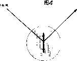
图1和2示出X射线衍射光谱的测量结果,所取的每个试样都是通过在c-平面蓝宝石衬底上制作的在<1-100>方向上以预定间隔延伸的长条形的SiO2掩模在c-平面蓝宝石衬底上以MOCVD方法生长GaN层制备而成的,并且一个试样上X射线的入射是在与掩模成水平的方向上(见图3),而在另一个试样上X射线的入射是在与掩模成垂直的方向上(见图4)。Figures 1 and 2 show the measurement results of X-ray diffraction spectra, each sample taken by making strips extending at predetermined intervals in the <1-100> direction on a c-plane sapphire substrate The SiO2 mask was prepared by growing a GaN layer on a c-plane sapphire substrate by MOCVD method, and the incidence of X-rays on a sample was in the direction horizontal to the mask (see Figure 3), while The incidence of X-rays on the other sample is in the direction perpendicular to the mask (see Figure 4).
由图1和2证实,尽管c-轴倾斜在X射线平行入射掩模的试样中显示单峰特性,但在X射线垂直入射掩模的试样中却显示多峰特性。通过透射电镜(TEM)分析发现,纵向晶轴在选择生长掩模区和无掩模区上的三个位置处发生偏斜,如图5所示。在图5中,掩模上的晶轴倾斜不限于所示的示例。It is confirmed from FIGS. 1 and 2 that although the c-axis tilt shows a unimodal characteristic in the sample of the X-ray parallel incident mask, it shows a multimodal characteristic in the sample of the X-ray normal incident mask. Through transmission electron microscopy (TEM) analysis, it was found that the longitudinal crystallographic axis was deflected at three positions on the selective growth masked area and the unmasked area, as shown in FIG. 5 . In FIG. 5, the crystal axis tilt on the mask is not limited to the example shown.
如选择生长薄膜包含晶轴的任何倾斜,特别是如果它包含如上所述的不连续变化,则可以推断沿边界引进了晶格缺陷,如位错。实际上,借助TEM观察到了位错,并且这种缺陷的引进或许就是制作于其上的半导体激光器特性恶化的因素。If the selectively grown film contains any tilt of the crystallographic axes, especially if it contains discontinuous changes as described above, it can be inferred that lattice defects such as dislocations have been introduced along the boundaries. In fact, dislocations were observed by means of TEM, and the introduction of such defects may be a factor of deterioration in the characteristics of semiconductor lasers fabricated thereon.
经过各种研究的结果本发明发现,采用氮化物来形成掩模的最外表面层可有效地防止在选择生长掩模上生长的薄膜的晶轴的倾斜。As a result of various investigations, the present inventors have found that the formation of the outermost surface layer of the mask using nitride is effective in preventing the inclination of the crystal axis of the thin film grown on the selective growth mask.
图6和7示出X射线衍射光谱的测量结果,所取的每个试样都是通过在c-平面蓝宝石衬底上制作的在<1-100>方向上以预定间隔延伸的长条形的SiO2上以堆积SiN薄膜方式形成的SiN/SiO2掩模在c-平面蓝宝石衬底上以MOCVD方法生长GaN层制备而成的,并且一个试样上X射线的入射是在与掩模成水平的方向上(见图3),而在另一个试样上X射线的入射是在与掩模成垂直的方向上(见图4)。Figures 6 and 7 show the measurement results of X-ray diffraction spectra, each sample taken by forming strips extending at predetermined intervals in the <1-100> direction on a c-plane sapphire substrate The SiN/SiO2 mask formed by stacking SiN thin films on SiO2 is prepared by growing GaN layer on c-plane sapphire substrate by MOCVD method, and the incidence of X-rays on a sample is in line with the mask In the horizontal direction (see Figure 3), the incidence of X-rays on the other sample is in the direction perpendicular to the mask (see Figure 4).
由图6和7证实,通过利用最外表面层是SiN的掩模进行的选择生长,则无论入射到掩模的X射线的方向是平行还是垂直,每个试样只显示一个代表晶轴倾斜的峰。除此之外,还证实代表晶轴倾斜变化的半高全宽值处于测量范围之内。这显示出选择生长薄膜的高结晶质量。It is confirmed by Figures 6 and 7 that by selective growth using a mask whose outermost surface layer is SiN, no matter whether the direction of X-rays incident on the mask is parallel or vertical, each sample only shows one crystal axis tilt peak. In addition to this, it was also confirmed that the value of the full width at half maximum representing the change in the tilt of the crystal axis was within the measurement range. This shows the high crystalline quality of the selectively grown films.
这并不意味着选择生长薄膜的晶轴如图5所示在每个区域都改变,但的确,如图8所示,显示纵向晶轴在整个选择生长薄膜上定向,并且整个薄膜质量均匀。This does not mean that the crystallographic axis of the selectively grown film changes in every region as shown in Figure 5, but indeed, as shown in Figure 8, shows that the longitudinal crystallographic axis is oriented throughout the selectively grown film and that the film quality is uniform throughout.
特别是在采用III-V族氮化物半导体的半导体发光器件中,如用作选择生长的掩模是采用氮化硅或氮化钛作为形成掩模的最外表面层并采用钛作为底层,选择生长比只采用钛作为选择生长掩模的情况要容易,因为是更稳定的氮化物形成表面。除此之外,当采用钛作为n侧电极时,在n型层中的通常只在横向方向上流动的电流很容易在纵向方向上流动。因此,其操作电压可降低。Especially in semiconductor light-emitting devices using III-V nitride semiconductors, if the mask used for selective growth is to use silicon nitride or titanium nitride as the outermost surface layer for forming the mask and titanium as the bottom layer, select Growth is easier than with only titanium as the selective growth mask because of the more stable nitride-forming surface. Besides, when titanium is used as the n-side electrode, current in the n-type layer, which normally flows only in the lateral direction, easily flows in the longitudinal direction. Therefore, its operating voltage can be lowered.
由图7B和7C可证实,与采用最外表面层是SiN的掩模的选择生长类似,甚至在采用最外表面层是TiN的掩模的选择生长中,每个试样都显示表示晶轴倾斜的单峰,无论是在平行于掩模的方向还是在垂直于掩模的方向。It can be confirmed from FIGS. 7B and 7C that, similarly to the selective growth using a mask whose outermost surface layer is SiN, even in the selective growth using a mask whose outermost surface layer is TiN, each sample shows a crystallographic axis A slanted single peak, either in the direction parallel to the mask or in the direction perpendicular to the mask.
除此之外,证实代表晶轴倾斜变化的半高全宽值处于测量范围之内。这显示出选择生长薄膜的高结晶质量。In addition to this, it was confirmed that the full width at half maximum value representing the crystal axis tilt change was within the measurement range. This shows the high crystalline quality of the selectively grown films.
本发明是通过发明人的这些研究而完成的。The present invention was accomplished through these studies by the inventors.
根据本发明的第一实施方案可提供一种用来在衬底上形成生长掩模并通过采用生长掩模在衬底上选择生长III-V族氮化物半导体的III-V族氮化物半导体的生长方法,其特征在于:According to the first embodiment of the present invention, there can be provided a method for forming a growth mask on a substrate and selectively growing a group III-V nitride semiconductor on the substrate by using the growth mask. A growing method characterized by:
采用至少其上表面由氮化物组成的多层薄膜作为生长掩模。A multilayer film whose at least upper surface is composed of nitride is used as a growth mask.
根据本发明的第二实施方案可提供一种半导体器件的制造方法用来在衬底上形成生长掩模并通过采用生长掩模在衬底上选择生长III-V族氮化物半导体,其特征在于:According to the second embodiment of the present invention, there can be provided a semiconductor device manufacturing method for forming a growth mask on a substrate and selectively growing a III-V group nitride semiconductor on the substrate by using the growth mask, characterized in that :
采用至少其上表面由氮化物组成的多层薄膜作为生长掩模。A multilayer film whose at least upper surface is composed of nitride is used as a growth mask.
根据本发明的第三实施方案可提供一种采用III-V族氮化物半导体的半导体器件,其特征在于:According to a third embodiment of the present invention, there can be provided a semiconductor device using a Group III-V nitride semiconductor, characterized in that:
在衬底上形成生长掩模,其中至少其上表面是氮化物,并且III-V族氮化物半导体是通过采用生长掩模在衬底上选择生长的。A growth mask is formed on a substrate in which at least an upper surface thereof is a nitride, and a group III-V nitride semiconductor is selectively grown on the substrate by using the growth mask.
在本发明中,在形成生长掩模的多层薄膜表面上的氮化物基本上可以是任何氮化物。但是,其具体例子是氧化硅(SiN)和氮化钛(TiN)。氮化物的厚度最好是在1nm至3μm的范围。多层薄膜可以是各种组合中的任何一种,比如氧化物薄膜和其上的氮化物薄膜的组合;金属薄膜和其上的氮化物薄膜的组合;氧化物薄膜,其上由氮化物和氧化物组成的薄膜,以及其上的氮化物薄膜的组合;以及第一金属薄膜,其上与第一金属薄膜不同的第二金属薄膜和其上的氮化物薄膜。氧化物薄膜比如可以是氧化硅薄膜,氮化物薄膜可以是金属氮化物薄膜,如氮化硅(SiN)薄膜或氮化钛(TiN)薄膜,金属薄膜可以是钛(Ti)薄膜或铂(Pt)薄膜,由氮化物和氧化物组成的薄膜,比如可以是缓变的氮氧化硅(SiN1-xOx(其中0<x<1))薄膜。如果愿意,这些多层薄膜中的任何一个都可以在一个或多个边界上在组分上是缓变的。In the present invention, the nitride on the surface of the multilayer thin film forming the growth mask may basically be any nitride. However, specific examples thereof are silicon oxide (SiN) and titanium nitride (TiN). The thickness of the nitride is preferably in the range of 1 nm to 3 µm. The multilayer film may be any of various combinations such as a combination of an oxide film and a nitride film thereon; a combination of a metal film and a nitride film thereon; an oxide film with a nitride and a nitride film thereon. A thin film composed of oxide and a combination of a nitride thin film thereon; and a first metal thin film, a second metal thin film different from the first metal thin film and a nitride thin film thereon. The oxide film can be, for example, a silicon oxide film, the nitride film can be a metal nitride film, such as a silicon nitride (SiN) film or a titanium nitride (TiN) film, and the metal film can be a titanium (Ti) film or a platinum (Pt) film. ) film, a film composed of nitride and oxide, such as a slowly changing silicon oxynitride (SiN1-x Ox (where 0<x<1)) film. Any of these multilayer films may be graded in composition at one or more boundaries, if desired.
生长掩模的构形可从各种构形中适当选择。其典型构形是相对衬底在一个方向上延伸的长条状。The configuration of the growth mask can be appropriately selected from various configurations. Its typical configuration is a long strip extending in one direction relative to the substrate.
在本发明中,在衬底上形成形式为包含氮化物用来至少形成其上表面的多层薄膜的第一生长掩模之后,在衬底上利用该第一生长掩模选择生长第一III-V族氮化物半导体,并在其后在衬底上第一生长掩模未覆盖的地方的上面形成形式为包含氮化物来至少在第一III-V族氮化物半导体上形成其上表面的多层薄膜的第二生长掩模,而第二III-V族氮化物半导体可借助第二生长掩模在第一III-V族氮化物半导体上选择生长。In the present invention, after forming a first growth mask on the substrate in the form of a multilayer thin film comprising nitride for forming at least the upper surface thereof, the first III is selectively grown on the substrate using the first growth mask. - a group V nitride semiconductor, and thereafter formed on the substrate above the places not covered by the first growth mask in the form of comprising nitride to form the upper surface thereof at least on the first III-V group nitride semiconductor The second growth mask of the multi-layer thin film, and the second III-V group nitride semiconductor can be selectively grown on the first III-V group nitride semiconductor by means of the second growth mask.
在本发明中,生长掩模可用作电极。在这种场合,生长掩模必须包含导电薄膜,如金属薄膜,作为其底层,或包含导电氮化物作为其上表面。生长掩模的具体的例子为金属薄膜和其上的氮化物薄膜的组合;金属薄膜,其上由氮化物和氧化物组成的薄膜,以及其上的氮化物薄膜的组合;第一金属薄膜,其上与第一金属薄膜不同的第二金属薄膜和其上的氮化物薄膜;氧化物薄膜和其上的氮化钛薄膜的组合;金属薄膜和其上的氮化钛薄膜的组合;氧化物薄膜,其上由氮化物和氧化物组成的薄膜,以及其上的氮化钛薄膜的组合;以及第一金属薄膜,其上与第一金属薄膜不同的第二金属薄膜和其上的氮化钛物薄膜。与前述相同的薄膜可用作氧化物薄膜、金属薄膜以及由氮化物和氧化物组成的薄膜。In the present invention, a growth mask can be used as an electrode. In this case, the growth mask must contain a conductive film, such as a metal film, as its bottom layer, or a conductive nitride as its upper surface. Specific examples of the growth mask are a metal thin film and a combination of a nitride thin film thereon; a metal thin film, a thin film made of nitride and an oxide thereon, and a combination of a nitride thin film thereon; a first metal thin film, A second metal film different from the first metal film thereon and a nitride film thereon; a combination of an oxide film and a titanium nitride film thereon; a combination of a metal film and a titanium nitride film thereon; an oxide a thin film, a combination of a thin film of nitride and an oxide thereon, and a titanium nitride thin film thereon; and a first metal thin film, a second metal thin film different from the first metal thin film thereon and a nitride nitride thereon Titanium film. The same thin films as mentioned above can be used as oxide thin films, metal thin films, and thin films composed of nitrides and oxides.
在本发明中,衬底可为蓝宝石衬底、SiC衬底、其上生长有或没有III-V族氮化物半导体的Si衬底或尖晶石衬底。In the present invention, the substrate may be a sapphire substrate, a SiC substrate, a Si substrate with or without group III-V nitride semiconductor grown thereon, or a spinel substrate.
在本发明中,可用作生长III-V族氮化物半导体的有金属有机物化学汽相淀积(MOCVD)、氢化物汽相外延(HVPE)以及分子束外延(MBE)。In the present invention, metal organic chemical vapor deposition (MOCVD), hydride vapor phase epitaxy (HVPE) and molecular beam epitaxy (MBE) can be used for growing III-V nitride semiconductors.
在本发明中,III-V族氮化物半导体由从Ga、Al、In、B及Tl一组中选择的至少一种III族元素以及一种或一种以上至少包含N并可能另外包含(如合适时)As或P的V族元素。III-V族氮化物半导体的具体例子为GaN、AlGaN、AlN、GaInN、AlGaInN及InN。In the present invention, the III-V group nitride semiconductor is composed of at least one group III element selected from the group of Ga, Al, In, B and Tl and one or more of which at least contain N and may additionally contain (such as As appropriate) Group V elements of As or P. Specific examples of group III-V nitride semiconductors are GaN, AlGaN, AlN, GaInN, AlGaInN, and InN.
在具有上面总结的结构的本发明中,由于包含至少形成其上表面的氮化物的多层薄膜是用作生长掩模,在选择生长III-V族氮化物半导体期间,在上表面上的氮化物使生长掩模的纵向晶轴定向,并从而减少生长层的纵向晶轴不规则定向。In the present invention having the structure summarized above, since the multilayer film containing nitride forming at least the upper surface thereof is used as a growth mask, during the selective growth of the III-V group nitride semiconductor, the nitrogen on the upper surface The compound orients the longitudinal crystallographic axis of the growth mask and thereby reduces the irregular orientation of the longitudinal crystallographic axis of the grown layer.
本发明的上述及其他目的、特征及优点,在参考附图阅读下面的本发明的详细描述时将会很容易了解。The above and other objects, features and advantages of the present invention will be readily understood when reading the following detailed description of the present invention with reference to the accompanying drawings.
附图简介Brief introduction to the drawings
图1为示出通过使X射线相对掩模平行入射到利用SiO2掩模作为生长掩模选择生长的GaN层上时对X射线衍射光谱的测量结果的曲线图;1 is a graph showing the measurement results of an X-ray diffraction spectrum when X-rays are incident parallel to a mask on a GaN layer selectively grown using aSiO mask as a growth mask;
图2为示出通过使X射线相对掩模垂直入射到利用SiO2掩模作为生长掩模选择生长的GaN层上时对X射线衍射光谱的测量结果的曲线图;2 is a graph showing the measurement results of X-ray diffraction spectra when X-rays are incident perpendicularly to the mask on a GaN layer selectively grown using aSiO mask as a growth mask;
图3为示出X射线相对掩模平行入射时的情况的示意图;Fig. 3 is a schematic diagram showing the situation when X-rays are incident parallel to the mask;
图4为示出X射线相对掩模垂直入射时的情况的示意图;Fig. 4 is a schematic diagram showing the situation when X-rays are perpendicularly incident on the mask;
图5示意地示出利用SiO2掩模作为生长掩模时选择生长的GaN层的晶轴的倾斜;Figure 5 schematically shows the inclination of the crystal axis of a selectively grown GaN layer using aSiO2 mask as a growth mask;
图6为示出通过使X射线相对掩模平行入射到利用SiN/SiO2掩模作为生长掩模选择生长的GaN层上时对X射线衍射光谱的测量结果的曲线图;6 is a graph showing the measurement results of X-ray diffraction spectra when X-rays are incident parallel to the mask on a GaN layer selectively grown using a SiN/SiO mask as a growth mask;
图7A为示出通过使X射线相对掩模垂直入射到利用SiN/SiO2掩模作为生长掩模选择生长的GaN层上时对X射线衍射光谱的测量结果的曲线图;7A is a graph showing the measurement results of the X-ray diffraction spectrum when X-rays are incident perpendicularly to the mask on a GaN layer selectively grown using a SiN/SiO mask as a growth mask;
图7B为示出通过使X射线相对掩模平行入射到利用SiN/SiO2掩模作为生长掩模选择生长的GaN层上时对X射线衍射光谱的测量结果的曲线图;7B is a graph showing the measurement results of the X-ray diffraction spectrum when X-rays are incident parallel to the mask on the GaN layer selectively grown using the SiN/SiO mask as the growth mask;
图7C为示出通过使X射线相对掩模垂直入射到利用TiN掩模作为生长掩模选择生长的GaN层上时对X射线衍射光谱的测量结果的曲线图;7C is a graph showing the measurement results of the X-ray diffraction spectrum when X-rays are perpendicularly incident on the GaN layer selectively grown using the TiN mask as the growth mask by making the X-rays perpendicularly incident on the mask;
图8为示意地示出利用包含至少氮化物形成其上表面的生长掩模选择生长的GaN层的晶轴的倾斜;8 schematically shows the inclination of the crystallographic axis of a GaN layer selectively grown using a growth mask comprising at least a nitride forming its upper surface;
图9为用于说明根据本发明第一实施方案的GaN化合物半导体激光器制造方法的剖视图;9 is a cross-sectional view for explaining a method of manufacturing a GaN compound semiconductor laser according to a first embodiment of the present invention;
图10为用于说明根据本发明第一实施方案的GaN化合物半导体激光器制造方法的剖视图;10 is a cross-sectional view for explaining a method of manufacturing a GaN compound semiconductor laser according to a first embodiment of the present invention;
图11为用于说明根据本发明第一实施方案的GaN化合物半导体激光器制造方法的剖视图;11 is a sectional view for explaining a method of manufacturing a GaN compound semiconductor laser according to the first embodiment of the present invention;
图12为用于说明根据本发明第一实施方案的GaN化合物半导体激光器制造方法的剖视图;12 is a cross-sectional view for explaining a method of manufacturing a GaN compound semiconductor laser according to the first embodiment of the present invention;
图13为用于说明根据本发明第一实施方案的GaN化合物半导体激光器制造方法的剖视图;13 is a cross-sectional view for explaining a method of manufacturing a GaN compound semiconductor laser according to the first embodiment of the present invention;
图14为用于说明根据本发明第一实施方案的GaN化合物半导体激光器制造方法的剖视图;14 is a cross-sectional view for explaining a method of manufacturing a GaN compound semiconductor laser according to the first embodiment of the present invention;
图15为用于说明根据本发明第一实施方案的GaN化合物半导体激光器中的电流通路的剖视图;15 is a sectional view for explaining a current path in the GaN compound semiconductor laser according to the first embodiment of the present invention;
图16为用于说明不采用导电生长掩模的GaN化合物半导体激光器中的电流通路的剖视图;16 is a cross-sectional view for explaining a current path in a GaN compound semiconductor laser not employing a conductive growth mask;
图17为用于说明根据本发明第二实施方案的GaN化合物半导体激光器制造方法的透视图。Fig. 17 is a perspective view for explaining a method of manufacturing a GaN compound semiconductor laser according to a second embodiment of the present invention.
优选实施方案的详细描述DETAILED DESCRIPTION OF THE PREFERRED EMBODIMENT
下面参考附图说明本发明的实施方案。在所有说明实施方案的附图中同一或等效元件采用同一标号。Embodiments of the present invention are described below with reference to the drawings. The same reference numerals are used for the same or equivalent elements in all figures illustrating the embodiments.
图9至图14示出根据本发明第一实施方案的GaN化合物半导体激光器制造方法。此处示出的GaN半导体激光器具有SCH结构(分别限制异质结构)。9 to 14 show a GaN compound semiconductor laser manufacturing method according to a first embodiment of the present invention. The GaN semiconductor laser shown here has an SCH structure (respectively confinement heterostructure).
在第一实施方案中,首先,如图9所示,在具有预先清洗过的表面的c-平面蓝宝石衬底1上生长包含未掺杂GaN层及n型GaN覆盖层的n型GaN/未掺杂GaN层2。为生长n型GaN/未掺杂GaN层2,可采用比如MOCVD、HVPE及MBE中任何一种。其次,在n型GaN/未掺杂GaN层2上顺序形成由氧化物和金属组成的第一薄膜3、由氮化物和氧化物组成的第二薄膜4以及由导电氮化物组成的第三薄膜5。更具体说来,比如,可采用SiO2薄膜、Ti薄膜或Pt薄膜作为第一薄膜3,比如,可采用SiN1-xOx(0<x<1)薄膜、Ti薄膜或Pt薄膜作为第二薄膜4,并且,比如,采用TiN薄膜或SiN薄膜作为第三薄膜5。由于由这些第一薄膜3、第二薄膜4和第三薄膜5组成的生长掩模用作后面将要说明的电极,第一薄膜3和第三薄膜5中至少一个必须是导电的。在采用金属薄膜,如TiN薄膜或SiN薄膜作为第一薄膜3的场合,比如,第三薄膜5可以是TiN薄膜或SiN薄膜中任何一个。如第一薄膜3是氧化物薄膜,如SiO2薄膜,第三薄膜5应该是导电的TiN薄膜。制作这些第一薄膜3、第二薄膜4和第三薄膜5,可采用比如真空蒸发、溅射或CVD工艺。用作第三薄膜5的TiN薄膜可直接形成或者首先制作Ti薄膜然后在热铵(NH3)中将Ti薄膜退火使其氮化。如需要,在制作第一薄膜3、第二薄膜4和第三薄膜5之前,比如使用氢氟酸对n型GaN/未掺杂GaN层进行腐蚀处理,以从其上去除尘埃或氧化膜。In the first embodiment, first, as shown in FIG. 9, an n-type GaN/undoped GaN layer including an undoped GaN layer and an n-type GaN capping layer is grown on a c-
其次,如图10所示,通过光刻在第三薄膜5上以预定间隔形成抗蚀图形6,其形状为垂直于半导体激光器的长条方向延伸的长条。抗蚀图形6的延伸方向可垂直于比如c-平面蓝宝石衬底1的<11-20>方向。Next, as shown in FIG. 10, resist
其次,如图11所示,利用抗蚀图形6作为掩模依次对第三薄膜5、 第二薄膜4和第一薄膜3进行刻蚀以形成包含这些第一薄膜3、第二薄膜4和第三薄膜5的生长掩模7。生长掩模7的宽度可适当确定为比如4.8μm。为对其进行刻蚀,可采用反应离子刻蚀(RIE)等干刻蚀或采用氢氟酸等刻蚀剂的湿法刻蚀。Next, as shown in Figure 11, use the resist
其次,如图12所示,去除抗蚀图形6。Next, as shown in FIG. 12, the resist
之后,已经形成生长掩模7的c-平面蓝宝石衬底1装入MOCVD装置的反应管内。此反应管比如由石英或不锈钢制作。同时装入反应管的可以有比如三甲基镓(TMG)或三乙基镓(TEGa)作为Ga的源材料,氢(H2)或氮(N2)作为载气,以及,比如硅烷(SiH4)作为n型掺杂剂。在此场合,为保证良好的选择生长,应调节源材料的供应量以便最好是将生长速率限制为不大于6μm。衬底温度设定为比如500℃至1200℃的范围内,应当注意,低于500℃的低温不能给提供已经形成生长掩模7的c-平面蓝宝石衬底1上的源材料足够的迁移能量,而超过1200℃的高温不能保证足够的生长速率,因为源材料的粘着系数过分降低并且不能保证反应管的安全。这样一来,如图13所示,在已经形成生长掩模7的n型GaN/未掺杂GaN层2上出现选择生长,可以得到纵向晶轴分布大大减小并且具有良好结晶质量的n型GaN层8的连续薄膜。After that, the c-
其次,在图14中,通过在n型GaN层8上顺序生长n型GaN层9、n型AlGaN包层10、n型GaN光波导层11、具有比如Ga1-xInxN/Ga1-yInyN多量子阱结构的有源层12、p型GaN光波导层13、p型AlGaN包层14及p型GaN接触层15。在此场合,由于作为它们的基层的n型GaN层是具有低晶体缺陷密度的高质量单晶材料,所以这些层也生长为具有低晶体缺陷密度的高质量单晶。对于生长不包含In的各层,即n型AlGaN包层10、n型GaN光波导层11、p型GaN光波导层13、p型AlGaN包层14及p型GaN接触层15,生长温度设定为比如大约1000℃,而对于生长包含In的层,即具有Ga1-xInxN/Ga1-yInyN多量子阱结构的有源层12,生长温度设定为比如大约700℃。在一个示例中,这些层的厚度分别为:n型GaN层9为3μm,n型AlGaN包层10为0.5μm,n型GaN光波导层11为0.1μm,p型GaN光波导层12为0.1μm,p型AlGaN包层14为0.5μm,而p型GaN接触层15为0.5μm。在n型AlGaN包层10和p型AlGaN包层14中Al组分比如为0.1。n型GaN层9、n型AlGaN包层10及n型GaN光波导层11比如用Si作为其施主进行掺杂,并且p型GaN光波导层13、p型AlGaN包层14及p型GaN接触层15比如用Mg作为其受主进行掺杂。之后,进行退火以便电激活经掺杂进入这些层的施主和受主,特别是掺杂到p型GaN光波导层13、p型AlGaN包层14和p型GaN接触层15中的受主。退火温度比如大约为700℃。Next, in FIG. 14 , by sequentially growing an n-
之后,在p型GaN接触层15上形成具有预定宽度的长条形抗蚀图形(图中未示出),比如在c-平面蓝宝石衬底1的<11-20>方向上延伸。利用抗蚀图形作为掩模,比如通过RIE对各层进行刻蚀,直到暴露出n型GaN/未掺杂GaN层2和生长掩模7以构图p型GaN接触层15、p型AlGaN包层14、p型GaN光波导层13、有源层12、n型GaN光波导层11、n型AlGaN包层10、n型GaN层9及n型GaN层8形成台面构造。Afterwards, a strip-shaped resist pattern (not shown) with a predetermined width is formed on the p-type
之后,去除用作抗蚀掩模的抗蚀图形。之后,在p型GaN接触层15上形成比如由Ni/Au薄膜或Ni/Pt/Au薄膜制作的p侧电极,并在n型GaN/未掺杂GaN层2及与台面部分邻接处的生长掩模7上形成比如由Ti/Al薄膜制作的n侧电极17。n侧电极17通过n型GaN/未掺杂GaN层2与n型GaN层8电连接。After that, the resist pattern used as a resist mask is removed. Afterwards, on the p-type
之后,用例如解理将通过这些步骤已经形成激光结构的c-平面蓝宝石衬底1分割成条,以便制作相对的腔缘,并在这些腔缘上涂敷腔缘涂层。之后,通过比如解理将每条分割为芯片。通过这些步骤所要求的具有SCH结构的GaN化合物半导体激光器就完成了。Thereafter, the c-
如上所述,根据本发明的第一实施方案,由于具有良好结晶质量纵向晶轴定向一致的n型GaN层8是利用生长掩模7通过选择生长而生长的,并且形成激光器结构的GaN化合物半导体层是在n型GaN层上生长的,所以可以实现性能优异寿命长可靠性高的GaN化合物半导体激光器。As described above, according to the first embodiment of the present invention, the n-
除此之外,在根据第一实施方案的GaN半导体激光器中,由于生长掩模7的顶层和底层至少一个是具有低电阻率的金属薄膜或TiN薄膜,在工作期间引入p侧电极16和n侧电极17之间的电流流过生长掩模7时的电阻很小,如图15所示。因此,n型GaN/未掺杂GaN层2的厚度和载流子浓度不会影响工作电压,因而就可能减小工作电压。这与图16中所示的激光器相比较就具有优越性,图16中的激光器没有采用在第一实施方案中的导电生长掩模,所以引入p侧电极16和n侧电极17之间的电流流入具有比金属和TiN薄膜的电阻率高的n型GaN/未掺杂GaN层,而工作电压就会受到n型GaN层8的厚度及载流子浓度的影响。In addition, in the GaN semiconductor laser according to the first embodiment, since at least one of the top layer and the bottom layer of the
下面说明根据本发明的第二实施方案的GaN半导体激光器的制作方法。此处示出的GaN半导体激光器具有SCH结构。A method of fabricating a GaN semiconductor laser according to a second embodiment of the present invention will be described below. The GaN semiconductor laser shown here has an SCH structure.
如图17所示,在第二实施方案中,生长掩模7是在平行于半导体激光器的长条方向上延伸而形成。生长掩模7是多层薄膜,其中至少上表面是由氮化物组成。在此场合,氮化物可以是导电的,也可以是绝缘的。与第一实施方案一样,n型GaN层8是利用生长掩模7选择生长的,并且n型GaN层9、n型AlGaN包层10、n型GaN光波导层11、具有比如Ga1-xInxN/Ga1-yInyN多量子阱结构的有源层12、p型GaN光波导层13、p型AlGaN包层14及p型GaN接触层15顺序生长在n型GaN层8上。As shown in FIG. 17, in the second embodiment, the
之后,在p型GaN接触层15上形成具有预定宽度的长条形抗蚀图形(图中未示出),比如在c-平面蓝宝石衬底1的<11-20>方向上延伸。利用抗蚀图形作为掩模,比如通过RIE对各层进行刻蚀,直到暴露出n型GaN层9以构图p型GaN接触层15、p型AlGaN包层14、p型GaN光波导层13、有源层12、n型GaN光波导层11及n型AlGaN包层1形成台面构造。Afterwards, a strip-shaped resist pattern (not shown) with a predetermined width is formed on the p-type
之后,去除用作抗蚀掩模的抗蚀图形。之后,在p型GaN接触层15上形成p侧电极,并在n型GaN层9与台面部分连接处上形成n侧电极17。After that, the resist pattern used as a resist mask is removed. Afterwards, a p-side electrode is formed on the p-type
之后,将通过这些步骤已经形成激光结构的c-平面蓝宝石衬底1比如经解理分割成条,以便制作相对的腔缘,并在这些腔缘上涂敷腔缘涂层。之后,比如通过解理将每条分割为芯片。通过这些步骤所要求的具有SCH结构的GaN化合物半导体激光器就完成了。Afterwards, the c-
如上所述,根据本发明的第二实施方案,由于具有良好结晶质量纵向晶轴定向一致的n型GaN层8是利用生长掩模7通过选择生长而生长的,并且形成激光器结构的GaN化合物半导体层是在n型GaN层上生长的,所以可以实现性能优异寿命长可靠性高的GaN化合物半导体激光器。As described above, according to the second embodiment of the present invention, the n-
上面参考附图描述了本发明的具体实施方案,但应当了解,本发明不受这些精确的实施方案的限制,并且在不脱离由后附的权利要求确定的本发明的范围和精神的情况下熟练的技术人员可以对其进行各种改变和修改。Specific embodiments of the present invention have been described above with reference to the accompanying drawings, but it should be understood that the present invention is not limited to these precise embodiments and does not depart from the scope and spirit of the invention as defined by the appended claims. Various changes and modifications can be made thereto by skilled artisans.
比如,在第一和第二实施方案中的上面中提出的数值、结构、衬底、源材料和加工过程只不过是示例,并且可以使用任何其他合适的数值、结构、衬底、源材料和加工过程。For example, the numerical values, structures, substrates, source materials, and processes set forth above in the first and second embodiments are merely examples, and any other suitable numerical values, structures, substrates, source materials, and processes may be used. Processing process.
在第一和第二实施方案中说明的生长掩模7是在c-平面蓝宝石衬底1的<11-20>方向上延伸。然而,长条形的生长掩模7的方向也可以比如是<1-100>方向。The
在第一和第二实施方案中,是利用c-平面蓝宝石衬底作为衬底。然而,如需要,也可使用比如SiC衬底、Si衬底或尖晶石衬底。In the first and second embodiments, a c-plane sapphire substrate is used as the substrate. However, a substrate such as SiC, Si, or spinel may also be used as necessary.
此外,说明第一和第二实施方案时是将本发明应用于GaN半导体激光器制造,但无须说,本发明也可用于制作GaN发光二极管,以及GaN化合物场效应晶体管及其他GaN化合物电子传递器件。In addition, the first and second embodiments were described as applying the present invention to the manufacture of GaN semiconductor lasers, but needless to say, the present invention is also applicable to the manufacture of GaN light emitting diodes, GaN compound field effect transistors and other GaN compound electron transfer devices.
如上所述,根据本发明的III-V族氮化物半导体的生长方法可利用至少在上表面形成有作为生长掩模的氮化物的多层薄膜来生长高质量低晶体缺陷密度的单晶III-V族氮化物半导体。As described above, the method for growing a group III-V nitride semiconductor according to the present invention can grow a high-quality, low-crystal defect density single crystal III- Group V nitride semiconductors.
此外,根据本发明的半导体器件的制作方法可利用至少在上表面形成有作为生长掩模的氮化物的多层薄膜来生长高质量低晶体缺陷密度的单晶III-V族氮化物半导体,并且因而可利用此种III-V族氮化物半导体制作具有良好特性的高性能半导体器件。In addition, the method for fabricating a semiconductor device according to the present invention can grow a high-quality, low-crystal-defect-density single-crystal III-V group nitride semiconductor using a multilayer thin film formed with nitride as a growth mask at least on the upper surface, and Therefore, high-performance semiconductor devices with good characteristics can be manufactured by using such III-V nitride semiconductors.
另外,利用根据本发明的半导体器件可使用利用至少在上表面形成有作为生长掩模的氮化物的多层薄膜来选择生长的高质量低晶体缺陷密度的单晶III-V族氮化物半导体制作具有良好特性的高性能半导体器件。In addition, a semiconductor device according to the present invention can be fabricated using a high-quality, low-crystal defect density single-crystal III-V nitride semiconductor selectively grown by using a multilayer thin film formed with a nitride as a growth mask at least on the upper surface. High-performance semiconductor devices with good characteristics.
Claims (38)
Translated fromChineseApplications Claiming Priority (2)
| Application Number | Priority Date | Filing Date | Title |
|---|---|---|---|
| JP335851/1998 | 1998-11-26 | ||
| JP33585198AJP3470623B2 (en) | 1998-11-26 | 1998-11-26 | Method for growing nitride III-V compound semiconductor, method for manufacturing semiconductor device, and semiconductor device |
Related Child Applications (1)
| Application Number | Title | Priority Date | Filing Date |
|---|---|---|---|
| CNB031278647ADivisionCN1302519C (en) | 1998-11-26 | 1999-11-26 | Manufacturing method of semiconductor device |
Publications (2)
| Publication Number | Publication Date |
|---|---|
| CN1258094Atrue CN1258094A (en) | 2000-06-28 |
| CN1147921C CN1147921C (en) | 2004-04-28 |
Family
ID=18293109
Family Applications (2)
| Application Number | Title | Priority Date | Filing Date |
|---|---|---|---|
| CNB031278647AExpired - LifetimeCN1302519C (en) | 1998-11-26 | 1999-11-26 | Manufacturing method of semiconductor device |
| CNB991243889AExpired - LifetimeCN1147921C (en) | 1998-11-26 | 1999-11-26 | Method for growing nitride semiconductor, semiconductor device and method for manufacturing the same |
Family Applications Before (1)
| Application Number | Title | Priority Date | Filing Date |
|---|---|---|---|
| CNB031278647AExpired - LifetimeCN1302519C (en) | 1998-11-26 | 1999-11-26 | Manufacturing method of semiconductor device |
Country Status (8)
| Country | Link |
|---|---|
| US (1) | US6682991B1 (en) |
| EP (1) | EP1005067B1 (en) |
| JP (1) | JP3470623B2 (en) |
| KR (1) | KR100724010B1 (en) |
| CN (2) | CN1302519C (en) |
| DE (1) | DE69936564T2 (en) |
| SG (1) | SG93850A1 (en) |
| TW (1) | TW429660B (en) |
Cited By (6)
| Publication number | Priority date | Publication date | Assignee | Title |
|---|---|---|---|---|
| US6955977B2 (en) | 1999-10-14 | 2005-10-18 | Cree, Inc. | Single step pendeo-and lateral epitaxial overgrowth of group III-nitride epitaxial layers with group III-nitride buffer layer and resulting structures |
| CN100372138C (en)* | 2005-07-13 | 2008-02-27 | 晶能光电(江西)有限公司 | Method for preparing high quality GaInAlN material on silicon substrate |
| CN100479099C (en)* | 2006-09-20 | 2009-04-15 | 财团法人工业技术研究院 | Nitride semiconductor substrate and method for manufacturing same |
| CN102354659A (en)* | 2011-11-02 | 2012-02-15 | 上海宏力半导体制造有限公司 | Method for eliminating nucleation on mask and selective epitaxial growth method |
| CN103165779A (en)* | 2013-02-08 | 2013-06-19 | 芜湖德豪润达光电科技有限公司 | Light emitting diode (LED) semiconductor element and manufacture method thereof |
| WO2021253284A1 (en)* | 2020-06-17 | 2021-12-23 | 华为技术有限公司 | Epitaxial wafer, led chip, and display screen |
Families Citing this family (28)
| Publication number | Priority date | Publication date | Assignee | Title |
|---|---|---|---|---|
| JP3702700B2 (en)* | 1999-03-31 | 2005-10-05 | 豊田合成株式会社 | Group III nitride compound semiconductor device and method for manufacturing the same |
| DE10056645B4 (en)* | 2000-11-09 | 2007-03-08 | Azzurro Semiconductors Ag | Process for the preparation of crack-free, planar group-III-N, group III-V-N and metal-nitrogen device structures on Si substrates by epitaxial methods |
| JP2003008143A (en)* | 2001-06-18 | 2003-01-10 | Sony Corp | Multi-beam semiconductor laser device |
| JP4767987B2 (en)* | 2002-12-05 | 2011-09-07 | 日本碍子株式会社 | Semiconductor stack structure and dislocation reduction method of group III nitride layer group |
| JP4457576B2 (en) | 2003-05-08 | 2010-04-28 | 住友電気工業株式会社 | Group III-V compound crystal and method for producing the same |
| WO2004107419A1 (en)* | 2003-05-30 | 2004-12-09 | Showa Denko K.K. | Method for production of group iii nitride semiconductor device |
| DE10335080A1 (en)* | 2003-07-31 | 2005-03-03 | Osram Opto Semiconductors Gmbh | Method for producing a multiplicity of optoelectronic semiconductor chips and optoelectronic semiconductor chip |
| DE10335081A1 (en) | 2003-07-31 | 2005-03-03 | Osram Opto Semiconductors Gmbh | Method for producing a multiplicity of optoelectronic semiconductor chips and optoelectronic semiconductor chip |
| US7638810B2 (en)* | 2005-09-09 | 2009-12-29 | Avago Technologies Ecbu Ip (Singapore) Pte. Ltd. | GaN laser with refractory metal ELOG masks for intracavity contact |
| CN100362133C (en)* | 2005-09-26 | 2008-01-16 | 中国地质大学(北京) | A kind of preparation method of hard wear-resistant protective film |
| CN100424224C (en)* | 2006-07-20 | 2008-10-08 | 上海交通大学 | Reaction and magnetically controlled sputtering process of preparing hard nanometer layered TiN/SiO2 coating |
| JP4884866B2 (en)* | 2006-07-25 | 2012-02-29 | 三菱電機株式会社 | Manufacturing method of nitride semiconductor device |
| US8362503B2 (en)* | 2007-03-09 | 2013-01-29 | Cree, Inc. | Thick nitride semiconductor structures with interlayer structures |
| CN102163667B (en)* | 2008-01-14 | 2014-04-16 | 晶元光电股份有限公司 | semiconductor light emitting structure |
| KR101449035B1 (en)* | 2008-04-30 | 2014-10-08 | 엘지이노텍 주식회사 | Semiconductor light emitting device |
| CN102044484A (en)* | 2009-10-23 | 2011-05-04 | 中芯国际集成电路制造(上海)有限公司 | Manufacturing method of tungsten plug on semiconductor device |
| JP5370279B2 (en)* | 2010-06-11 | 2013-12-18 | 豊田合成株式会社 | Method for producing n-type group III nitride semiconductor |
| JP2015521365A (en)* | 2012-04-13 | 2015-07-27 | タンデム スン アーベー | Manufacturing method of semiconductor method device based on epitaxial growth |
| KR102075986B1 (en)* | 2014-02-03 | 2020-02-11 | 삼성전자주식회사 | Emiconductor light emitting device |
| JP2016171265A (en)* | 2015-03-13 | 2016-09-23 | 株式会社東芝 | Semiconductor device and manufacturing method of the same |
| CN105633790A (en)* | 2016-03-09 | 2016-06-01 | 中国科学院合肥物质科学研究院 | Method for realizing visible laser by GaN laser diode pumping rare earth ion doped tantalate-niobate |
| US10707308B2 (en) | 2017-12-24 | 2020-07-07 | HangZhou HaiCun Information Technology Co., Ltd. | Hetero-epitaxial output device array |
| US11177549B2 (en)* | 2019-11-06 | 2021-11-16 | International Business Machines Corporation | Method of growing titanium nitride on silicon substrate free from silicon nitride interface by using a titanium seed layer |
| CN112103305B (en)* | 2020-09-21 | 2022-05-27 | 中国科学院长春光学精密机械与物理研究所 | Micro-LED array based on Micro-patterned graphene, preparation method of Micro-LED array and display device |
| JP7556246B2 (en) | 2020-09-23 | 2024-09-26 | セイコーエプソン株式会社 | Light emitting device, method for manufacturing the same, and projector |
| JPWO2024095458A1 (en)* | 2022-11-04 | 2024-05-10 | ||
| WO2024157687A1 (en)* | 2023-01-25 | 2024-08-02 | 株式会社ジャパンディスプレイ | Light-emitting device and manufacturing method therefor |
| WO2025185824A1 (en)* | 2024-03-07 | 2025-09-12 | Ams-Osram International Gmbh | Method of processing an optoelectronic device and optoelectronic device |
Family Cites Families (14)
| Publication number | Priority date | Publication date | Assignee | Title |
|---|---|---|---|---|
| NL7412383A (en)* | 1974-09-19 | 1976-03-23 | Philips Nv | METHOD OF MANUFACTURING A DEVICE WITH A CONDUCTOR PATTERN. |
| FR2580672B1 (en)* | 1985-04-19 | 1987-05-15 | France Etat | METHOD FOR MANUFACTURING ON AN INSULATING SUPPORT OF A SINGLE-CRYSTAL, LOCAL-DEFECT SILICON FILM |
| US5326716A (en)* | 1986-02-11 | 1994-07-05 | Max Planck-Gesellschaft Zur Foerderung Der Wissenschaften E.V. | Liquid phase epitaxial process for producing three-dimensional semiconductor structures by liquid phase expitaxy |
| FR2629637B1 (en)* | 1988-04-05 | 1990-11-16 | Thomson Csf | METHOD FOR PRODUCING AN ALTERNATION OF LAYERS OF SINGLE-CRYSTAL SEMICONDUCTOR MATERIAL AND LAYERS OF INSULATING MATERIAL |
| JPH02159775A (en)* | 1988-12-14 | 1990-06-19 | Toshiba Corp | Semiconductor photodetector and its manufacturing method |
| FR2645345A1 (en)* | 1989-03-31 | 1990-10-05 | Thomson Csf | METHOD FOR DIRECT MODULATION OF THE COMPOSITION OR DOPING OF SEMICONDUCTORS, IN PARTICULAR FOR THE PRODUCTION OF ELECTRONIC MONOLITHIC COMPONENTS OF THE PLANAR TYPE, USE AND CORRESPONDING PRODUCTS |
| US4971928A (en)* | 1990-01-16 | 1990-11-20 | General Motors Corporation | Method of making a light emitting semiconductor having a rear reflecting surface |
| US5208167A (en)* | 1991-09-30 | 1993-05-04 | Rohm Co., Ltd. | Method for producing SOI substrate |
| JPH1022568A (en)* | 1996-07-04 | 1998-01-23 | Hitachi Ltd | Semiconductor device |
| JP3925753B2 (en)* | 1997-10-24 | 2007-06-06 | ソニー株式会社 | Semiconductor device, manufacturing method thereof, and semiconductor light emitting device |
| US6271104B1 (en)* | 1998-08-10 | 2001-08-07 | Mp Technologies | Fabrication of defect free III-nitride materials |
| US6240115B1 (en)* | 1998-08-27 | 2001-05-29 | Agilent Technologies, Inc. | Epitaxial facet formation for laser diodes based on III-V material systems |
| JP3019085B1 (en) | 1998-10-09 | 2000-03-13 | サンケン電気株式会社 | Semiconductor light emitting device and method of manufacturing the same |
| US6255198B1 (en)* | 1998-11-24 | 2001-07-03 | North Carolina State University | Methods of fabricating gallium nitride microelectronic layers on silicon layers and gallium nitride microelectronic structures formed thereby |
- 1998
- 1998-11-26JPJP33585198Apatent/JP3470623B2/ennot_activeExpired - Lifetime
- 1999
- 1999-11-19TWTW088120266Apatent/TW429660B/ennot_activeIP Right Cessation
- 1999-11-19SGSG9905771Apatent/SG93850A1/enunknown
- 1999-11-23EPEP99123367Apatent/EP1005067B1/ennot_activeExpired - Lifetime
- 1999-11-23DEDE69936564Tpatent/DE69936564T2/ennot_activeExpired - Lifetime
- 1999-11-24USUS09/448,584patent/US6682991B1/ennot_activeExpired - Lifetime
- 1999-11-25KRKR1019990052590Apatent/KR100724010B1/ennot_activeExpired - Lifetime
- 1999-11-26CNCNB031278647Apatent/CN1302519C/ennot_activeExpired - Lifetime
- 1999-11-26CNCNB991243889Apatent/CN1147921C/ennot_activeExpired - Lifetime
Cited By (9)
| Publication number | Priority date | Publication date | Assignee | Title |
|---|---|---|---|---|
| US6955977B2 (en) | 1999-10-14 | 2005-10-18 | Cree, Inc. | Single step pendeo-and lateral epitaxial overgrowth of group III-nitride epitaxial layers with group III-nitride buffer layer and resulting structures |
| CN100372138C (en)* | 2005-07-13 | 2008-02-27 | 晶能光电(江西)有限公司 | Method for preparing high quality GaInAlN material on silicon substrate |
| CN100479099C (en)* | 2006-09-20 | 2009-04-15 | 财团法人工业技术研究院 | Nitride semiconductor substrate and method for manufacturing same |
| CN102354659A (en)* | 2011-11-02 | 2012-02-15 | 上海宏力半导体制造有限公司 | Method for eliminating nucleation on mask and selective epitaxial growth method |
| CN102354659B (en)* | 2011-11-02 | 2016-05-11 | 上海华虹宏力半导体制造有限公司 | Mask nucleation removing method and selective epitaxial growth method |
| CN103165779A (en)* | 2013-02-08 | 2013-06-19 | 芜湖德豪润达光电科技有限公司 | Light emitting diode (LED) semiconductor element and manufacture method thereof |
| CN103165779B (en)* | 2013-02-08 | 2016-04-06 | 芜湖德豪润达光电科技有限公司 | LED semiconductor element and manufacture method thereof |
| WO2021253284A1 (en)* | 2020-06-17 | 2021-12-23 | 华为技术有限公司 | Epitaxial wafer, led chip, and display screen |
| CN115443521A (en)* | 2020-06-17 | 2022-12-06 | 华为技术有限公司 | Epitaxial wafer, LED chip and display screen |
Also Published As
| Publication number | Publication date |
|---|---|
| KR100724010B1 (en) | 2007-05-31 |
| SG93850A1 (en) | 2003-01-21 |
| KR20000035670A (en) | 2000-06-26 |
| DE69936564D1 (en) | 2007-08-30 |
| EP1005067A3 (en) | 2000-10-18 |
| EP1005067A2 (en) | 2000-05-31 |
| JP2000164988A (en) | 2000-06-16 |
| TW429660B (en) | 2001-04-11 |
| CN1147921C (en) | 2004-04-28 |
| US6682991B1 (en) | 2004-01-27 |
| EP1005067B1 (en) | 2007-07-18 |
| CN1302519C (en) | 2007-02-28 |
| JP3470623B2 (en) | 2003-11-25 |
| DE69936564T2 (en) | 2008-04-03 |
| CN1501444A (en) | 2004-06-02 |
Similar Documents
| Publication | Publication Date | Title |
|---|---|---|
| CN1258094A (en) | Growth method of nitride semiconductor, semiconductor device and manufacturing method thereof | |
| US6841410B2 (en) | Method for forming group-III nitride semiconductor layer and group-III nitride semiconductor device | |
| US6586819B2 (en) | Sapphire substrate, semiconductor device, electronic component, and crystal growing method | |
| JP5280004B2 (en) | Light emitting device and manufacturing method thereof | |
| US6380051B1 (en) | Layered structure including a nitride compound semiconductor film and method for making the same | |
| US6673478B2 (en) | Crystal-growth substrate and a ZnO-containing compound semiconductor device | |
| KR100449074B1 (en) | Method for manufacturing semiconductor and semiconductor light emitting element | |
| EP2684988A1 (en) | Base, substrate with gallium nitride crystal layer, and process for producing same | |
| US7183578B2 (en) | Semiconductor apparatus, method for growing nitride semiconductor and method for producing semiconductor apparatus | |
| JP2005286338A (en) | 4H type polytype gallium nitride based semiconductor device formed on 4H type polytype substrate | |
| US8030682B2 (en) | Zinc-blende nitride semiconductor free-standing substrate, method for fabricating same, and light-emitting device employing same | |
| JP2003229645A (en) | Quantum well structure, semiconductor device using the same, and method of manufacturing semiconductor device | |
| US7759219B2 (en) | Method of manufacturing nitride semiconductor device | |
| CN1533002A (en) | Nitride semiconductor device manufacturing method | |
| JP4883931B2 (en) | Manufacturing method of semiconductor laminated substrate | |
| US8134223B2 (en) | III-V compound crystal and semiconductor electronic circuit element | |
| JP4631214B2 (en) | Manufacturing method of nitride semiconductor film | |
| JP4583523B2 (en) | III-V nitride semiconductor light emitting device and method for manufacturing the same | |
| JP2000174343A (en) | Method for manufacturing nitride semiconductor and light emitting device | |
| JP4232326B2 (en) | Method for growing low-defect nitride semiconductor | |
| JP2001308464A (en) | Nitride semiconductor element, method for manufacturing nitride semiconductor crystal, and nitride semiconductor substrate | |
| JP2002270970A (en) | Nitride semiconductor light emitting device | |
| CN1846299A (en) | Nitride semiconductor substrate and nitride semiconductor device using same | |
| JP2003289047A (en) | Method for growing nitride system group iii-v compound semiconductor and method for manufacturing semiconductor device and semiconductor device | |
| JPH11274649A (en) | Semiconductor optical device and method of manufacturing the same |
Legal Events
| Date | Code | Title | Description |
|---|---|---|---|
| C06 | Publication | ||
| PB01 | Publication | ||
| C10 | Entry into substantive examination | ||
| SE01 | Entry into force of request for substantive examination | ||
| C14 | Grant of patent or utility model | ||
| GR01 | Patent grant | ||
| CX01 | Expiry of patent term | Granted publication date:20040428 | |
| CX01 | Expiry of patent term |