CN1237785A - Semiconductor device and manufacturing method of semiconductor device - Google Patents
Semiconductor device and manufacturing method of semiconductor deviceDownload PDFInfo
- Publication number
- CN1237785A CN1237785ACN99106938ACN99106938ACN1237785ACN 1237785 ACN1237785 ACN 1237785ACN 99106938 ACN99106938 ACN 99106938ACN 99106938 ACN99106938 ACN 99106938ACN 1237785 ACN1237785 ACN 1237785A
- Authority
- CN
- China
- Prior art keywords
- lead
- semiconductor chip
- lead frame
- semiconductor
- interior section
- Prior art date
- Legal status (The legal status is an assumption and is not a legal conclusion. Google has not performed a legal analysis and makes no representation as to the accuracy of the status listed.)
- Pending
Links
Images


Classifications
- H—ELECTRICITY
- H01—ELECTRIC ELEMENTS
- H01L—SEMICONDUCTOR DEVICES NOT COVERED BY CLASS H10
- H01L21/00—Processes or apparatus adapted for the manufacture or treatment of semiconductor or solid state devices or of parts thereof
- H01L21/02—Manufacture or treatment of semiconductor devices or of parts thereof
- H01L21/04—Manufacture or treatment of semiconductor devices or of parts thereof the devices having potential barriers, e.g. a PN junction, depletion layer or carrier concentration layer
- H01L21/50—Assembly of semiconductor devices using processes or apparatus not provided for in a single one of the groups H01L21/18 - H01L21/326 or H10D48/04 - H10D48/07 e.g. sealing of a cap to a base of a container
- H01L21/56—Encapsulations, e.g. encapsulation layers, coatings
- H01L21/565—Moulds
- H—ELECTRICITY
- H01—ELECTRIC ELEMENTS
- H01L—SEMICONDUCTOR DEVICES NOT COVERED BY CLASS H10
- H01L23/00—Details of semiconductor or other solid state devices
- H01L23/28—Encapsulations, e.g. encapsulating layers, coatings, e.g. for protection
- H—ELECTRICITY
- H01—ELECTRIC ELEMENTS
- H01L—SEMICONDUCTOR DEVICES NOT COVERED BY CLASS H10
- H01L23/00—Details of semiconductor or other solid state devices
- H01L23/48—Arrangements for conducting electric current to or from the solid state body in operation, e.g. leads, terminal arrangements ; Selection of materials therefor
- H01L23/488—Arrangements for conducting electric current to or from the solid state body in operation, e.g. leads, terminal arrangements ; Selection of materials therefor consisting of soldered or bonded constructions
- H01L23/495—Lead-frames or other flat leads
- H01L23/49503—Lead-frames or other flat leads characterised by the die pad
- H01L23/4951—Chip-on-leads or leads-on-chip techniques, i.e. inner lead fingers being used as die pad
- H—ELECTRICITY
- H01—ELECTRIC ELEMENTS
- H01L—SEMICONDUCTOR DEVICES NOT COVERED BY CLASS H10
- H01L23/00—Details of semiconductor or other solid state devices
- H01L23/48—Arrangements for conducting electric current to or from the solid state body in operation, e.g. leads, terminal arrangements ; Selection of materials therefor
- H01L23/488—Arrangements for conducting electric current to or from the solid state body in operation, e.g. leads, terminal arrangements ; Selection of materials therefor consisting of soldered or bonded constructions
- H01L23/495—Lead-frames or other flat leads
- H01L23/49537—Plurality of lead frames mounted in one device
- H—ELECTRICITY
- H01—ELECTRIC ELEMENTS
- H01L—SEMICONDUCTOR DEVICES NOT COVERED BY CLASS H10
- H01L23/00—Details of semiconductor or other solid state devices
- H01L23/48—Arrangements for conducting electric current to or from the solid state body in operation, e.g. leads, terminal arrangements ; Selection of materials therefor
- H01L23/488—Arrangements for conducting electric current to or from the solid state body in operation, e.g. leads, terminal arrangements ; Selection of materials therefor consisting of soldered or bonded constructions
- H01L23/495—Lead-frames or other flat leads
- H01L23/49575—Assemblies of semiconductor devices on lead frames
- H—ELECTRICITY
- H01—ELECTRIC ELEMENTS
- H01L—SEMICONDUCTOR DEVICES NOT COVERED BY CLASS H10
- H01L24/00—Arrangements for connecting or disconnecting semiconductor or solid-state bodies; Methods or apparatus related thereto
- H01L24/01—Means for bonding being attached to, or being formed on, the surface to be connected, e.g. chip-to-package, die-attach, "first-level" interconnects; Manufacturing methods related thereto
- H01L24/02—Bonding areas ; Manufacturing methods related thereto
- H01L24/04—Structure, shape, material or disposition of the bonding areas prior to the connecting process
- H01L24/05—Structure, shape, material or disposition of the bonding areas prior to the connecting process of an individual bonding area
- H—ELECTRICITY
- H01—ELECTRIC ELEMENTS
- H01L—SEMICONDUCTOR DEVICES NOT COVERED BY CLASS H10
- H01L24/00—Arrangements for connecting or disconnecting semiconductor or solid-state bodies; Methods or apparatus related thereto
- H01L24/01—Means for bonding being attached to, or being formed on, the surface to be connected, e.g. chip-to-package, die-attach, "first-level" interconnects; Manufacturing methods related thereto
- H01L24/02—Bonding areas ; Manufacturing methods related thereto
- H01L24/04—Structure, shape, material or disposition of the bonding areas prior to the connecting process
- H01L24/06—Structure, shape, material or disposition of the bonding areas prior to the connecting process of a plurality of bonding areas
- H—ELECTRICITY
- H01—ELECTRIC ELEMENTS
- H01L—SEMICONDUCTOR DEVICES NOT COVERED BY CLASS H10
- H01L24/00—Arrangements for connecting or disconnecting semiconductor or solid-state bodies; Methods or apparatus related thereto
- H01L24/01—Means for bonding being attached to, or being formed on, the surface to be connected, e.g. chip-to-package, die-attach, "first-level" interconnects; Manufacturing methods related thereto
- H01L24/42—Wire connectors; Manufacturing methods related thereto
- H01L24/47—Structure, shape, material or disposition of the wire connectors after the connecting process
- H01L24/49—Structure, shape, material or disposition of the wire connectors after the connecting process of a plurality of wire connectors
- H—ELECTRICITY
- H01—ELECTRIC ELEMENTS
- H01L—SEMICONDUCTOR DEVICES NOT COVERED BY CLASS H10
- H01L2224/00—Indexing scheme for arrangements for connecting or disconnecting semiconductor or solid-state bodies and methods related thereto as covered by H01L24/00
- H01L2224/01—Means for bonding being attached to, or being formed on, the surface to be connected, e.g. chip-to-package, die-attach, "first-level" interconnects; Manufacturing methods related thereto
- H01L2224/02—Bonding areas; Manufacturing methods related thereto
- H01L2224/04—Structure, shape, material or disposition of the bonding areas prior to the connecting process
- H01L2224/04042—Bonding areas specifically adapted for wire connectors, e.g. wirebond pads
- H—ELECTRICITY
- H01—ELECTRIC ELEMENTS
- H01L—SEMICONDUCTOR DEVICES NOT COVERED BY CLASS H10
- H01L2224/00—Indexing scheme for arrangements for connecting or disconnecting semiconductor or solid-state bodies and methods related thereto as covered by H01L24/00
- H01L2224/01—Means for bonding being attached to, or being formed on, the surface to be connected, e.g. chip-to-package, die-attach, "first-level" interconnects; Manufacturing methods related thereto
- H01L2224/02—Bonding areas; Manufacturing methods related thereto
- H01L2224/04—Structure, shape, material or disposition of the bonding areas prior to the connecting process
- H01L2224/05—Structure, shape, material or disposition of the bonding areas prior to the connecting process of an individual bonding area
- H01L2224/0554—External layer
- H01L2224/0555—Shape
- H01L2224/05552—Shape in top view
- H01L2224/05554—Shape in top view being square
- H—ELECTRICITY
- H01—ELECTRIC ELEMENTS
- H01L—SEMICONDUCTOR DEVICES NOT COVERED BY CLASS H10
- H01L2224/00—Indexing scheme for arrangements for connecting or disconnecting semiconductor or solid-state bodies and methods related thereto as covered by H01L24/00
- H01L2224/01—Means for bonding being attached to, or being formed on, the surface to be connected, e.g. chip-to-package, die-attach, "first-level" interconnects; Manufacturing methods related thereto
- H01L2224/02—Bonding areas; Manufacturing methods related thereto
- H01L2224/04—Structure, shape, material or disposition of the bonding areas prior to the connecting process
- H01L2224/05—Structure, shape, material or disposition of the bonding areas prior to the connecting process of an individual bonding area
- H01L2224/0554—External layer
- H01L2224/05599—Material
- H01L2224/056—Material with a principal constituent of the material being a metal or a metalloid, e.g. boron [B], silicon [Si], germanium [Ge], arsenic [As], antimony [Sb], tellurium [Te] and polonium [Po], and alloys thereof
- H01L2224/05617—Material with a principal constituent of the material being a metal or a metalloid, e.g. boron [B], silicon [Si], germanium [Ge], arsenic [As], antimony [Sb], tellurium [Te] and polonium [Po], and alloys thereof the principal constituent melting at a temperature of greater than or equal to 400°C and less than 950°C
- H01L2224/05624—Aluminium [Al] as principal constituent
- H—ELECTRICITY
- H01—ELECTRIC ELEMENTS
- H01L—SEMICONDUCTOR DEVICES NOT COVERED BY CLASS H10
- H01L2224/00—Indexing scheme for arrangements for connecting or disconnecting semiconductor or solid-state bodies and methods related thereto as covered by H01L24/00
- H01L2224/01—Means for bonding being attached to, or being formed on, the surface to be connected, e.g. chip-to-package, die-attach, "first-level" interconnects; Manufacturing methods related thereto
- H01L2224/02—Bonding areas; Manufacturing methods related thereto
- H01L2224/04—Structure, shape, material or disposition of the bonding areas prior to the connecting process
- H01L2224/06—Structure, shape, material or disposition of the bonding areas prior to the connecting process of a plurality of bonding areas
- H01L2224/061—Disposition
- H01L2224/0612—Layout
- H01L2224/0613—Square or rectangular array
- H01L2224/06134—Square or rectangular array covering only portions of the surface to be connected
- H01L2224/06136—Covering only the central area of the surface to be connected, i.e. central arrangements
- H—ELECTRICITY
- H01—ELECTRIC ELEMENTS
- H01L—SEMICONDUCTOR DEVICES NOT COVERED BY CLASS H10
- H01L2224/00—Indexing scheme for arrangements for connecting or disconnecting semiconductor or solid-state bodies and methods related thereto as covered by H01L24/00
- H01L2224/01—Means for bonding being attached to, or being formed on, the surface to be connected, e.g. chip-to-package, die-attach, "first-level" interconnects; Manufacturing methods related thereto
- H01L2224/26—Layer connectors, e.g. plate connectors, solder or adhesive layers; Manufacturing methods related thereto
- H01L2224/31—Structure, shape, material or disposition of the layer connectors after the connecting process
- H01L2224/32—Structure, shape, material or disposition of the layer connectors after the connecting process of an individual layer connector
- H01L2224/321—Disposition
- H01L2224/32151—Disposition the layer connector connecting between a semiconductor or solid-state body and an item not being a semiconductor or solid-state body, e.g. chip-to-substrate, chip-to-passive
- H01L2224/32221—Disposition the layer connector connecting between a semiconductor or solid-state body and an item not being a semiconductor or solid-state body, e.g. chip-to-substrate, chip-to-passive the body and the item being stacked
- H01L2224/32245—Disposition the layer connector connecting between a semiconductor or solid-state body and an item not being a semiconductor or solid-state body, e.g. chip-to-substrate, chip-to-passive the body and the item being stacked the item being metallic
- H—ELECTRICITY
- H01—ELECTRIC ELEMENTS
- H01L—SEMICONDUCTOR DEVICES NOT COVERED BY CLASS H10
- H01L2224/00—Indexing scheme for arrangements for connecting or disconnecting semiconductor or solid-state bodies and methods related thereto as covered by H01L24/00
- H01L2224/01—Means for bonding being attached to, or being formed on, the surface to be connected, e.g. chip-to-package, die-attach, "first-level" interconnects; Manufacturing methods related thereto
- H01L2224/42—Wire connectors; Manufacturing methods related thereto
- H01L2224/44—Structure, shape, material or disposition of the wire connectors prior to the connecting process
- H01L2224/45—Structure, shape, material or disposition of the wire connectors prior to the connecting process of an individual wire connector
- H01L2224/45001—Core members of the connector
- H01L2224/4501—Shape
- H01L2224/45012—Cross-sectional shape
- H01L2224/45015—Cross-sectional shape being circular
- H—ELECTRICITY
- H01—ELECTRIC ELEMENTS
- H01L—SEMICONDUCTOR DEVICES NOT COVERED BY CLASS H10
- H01L2224/00—Indexing scheme for arrangements for connecting or disconnecting semiconductor or solid-state bodies and methods related thereto as covered by H01L24/00
- H01L2224/01—Means for bonding being attached to, or being formed on, the surface to be connected, e.g. chip-to-package, die-attach, "first-level" interconnects; Manufacturing methods related thereto
- H01L2224/42—Wire connectors; Manufacturing methods related thereto
- H01L2224/44—Structure, shape, material or disposition of the wire connectors prior to the connecting process
- H01L2224/45—Structure, shape, material or disposition of the wire connectors prior to the connecting process of an individual wire connector
- H01L2224/45001—Core members of the connector
- H01L2224/45099—Material
- H01L2224/451—Material with a principal constituent of the material being a metal or a metalloid, e.g. boron (B), silicon (Si), germanium (Ge), arsenic (As), antimony (Sb), tellurium (Te) and polonium (Po), and alloys thereof
- H01L2224/45138—Material with a principal constituent of the material being a metal or a metalloid, e.g. boron (B), silicon (Si), germanium (Ge), arsenic (As), antimony (Sb), tellurium (Te) and polonium (Po), and alloys thereof the principal constituent melting at a temperature of greater than or equal to 950°C and less than 1550°C
- H01L2224/45144—Gold (Au) as principal constituent
- H—ELECTRICITY
- H01—ELECTRIC ELEMENTS
- H01L—SEMICONDUCTOR DEVICES NOT COVERED BY CLASS H10
- H01L2224/00—Indexing scheme for arrangements for connecting or disconnecting semiconductor or solid-state bodies and methods related thereto as covered by H01L24/00
- H01L2224/01—Means for bonding being attached to, or being formed on, the surface to be connected, e.g. chip-to-package, die-attach, "first-level" interconnects; Manufacturing methods related thereto
- H01L2224/42—Wire connectors; Manufacturing methods related thereto
- H01L2224/47—Structure, shape, material or disposition of the wire connectors after the connecting process
- H01L2224/48—Structure, shape, material or disposition of the wire connectors after the connecting process of an individual wire connector
- H01L2224/4805—Shape
- H01L2224/4809—Loop shape
- H01L2224/48091—Arched
- H—ELECTRICITY
- H01—ELECTRIC ELEMENTS
- H01L—SEMICONDUCTOR DEVICES NOT COVERED BY CLASS H10
- H01L2224/00—Indexing scheme for arrangements for connecting or disconnecting semiconductor or solid-state bodies and methods related thereto as covered by H01L24/00
- H01L2224/01—Means for bonding being attached to, or being formed on, the surface to be connected, e.g. chip-to-package, die-attach, "first-level" interconnects; Manufacturing methods related thereto
- H01L2224/42—Wire connectors; Manufacturing methods related thereto
- H01L2224/47—Structure, shape, material or disposition of the wire connectors after the connecting process
- H01L2224/48—Structure, shape, material or disposition of the wire connectors after the connecting process of an individual wire connector
- H01L2224/481—Disposition
- H01L2224/48151—Connecting between a semiconductor or solid-state body and an item not being a semiconductor or solid-state body, e.g. chip-to-substrate, chip-to-passive
- H01L2224/48221—Connecting between a semiconductor or solid-state body and an item not being a semiconductor or solid-state body, e.g. chip-to-substrate, chip-to-passive the body and the item being stacked
- H01L2224/48245—Connecting between a semiconductor or solid-state body and an item not being a semiconductor or solid-state body, e.g. chip-to-substrate, chip-to-passive the body and the item being stacked the item being metallic
- H01L2224/48247—Connecting between a semiconductor or solid-state body and an item not being a semiconductor or solid-state body, e.g. chip-to-substrate, chip-to-passive the body and the item being stacked the item being metallic connecting the wire to a bond pad of the item
- H—ELECTRICITY
- H01—ELECTRIC ELEMENTS
- H01L—SEMICONDUCTOR DEVICES NOT COVERED BY CLASS H10
- H01L2224/00—Indexing scheme for arrangements for connecting or disconnecting semiconductor or solid-state bodies and methods related thereto as covered by H01L24/00
- H01L2224/01—Means for bonding being attached to, or being formed on, the surface to be connected, e.g. chip-to-package, die-attach, "first-level" interconnects; Manufacturing methods related thereto
- H01L2224/42—Wire connectors; Manufacturing methods related thereto
- H01L2224/47—Structure, shape, material or disposition of the wire connectors after the connecting process
- H01L2224/48—Structure, shape, material or disposition of the wire connectors after the connecting process of an individual wire connector
- H01L2224/481—Disposition
- H01L2224/48151—Connecting between a semiconductor or solid-state body and an item not being a semiconductor or solid-state body, e.g. chip-to-substrate, chip-to-passive
- H01L2224/48221—Connecting between a semiconductor or solid-state body and an item not being a semiconductor or solid-state body, e.g. chip-to-substrate, chip-to-passive the body and the item being stacked
- H01L2224/48245—Connecting between a semiconductor or solid-state body and an item not being a semiconductor or solid-state body, e.g. chip-to-substrate, chip-to-passive the body and the item being stacked the item being metallic
- H01L2224/4826—Connecting between the body and an opposite side of the item with respect to the body
- H—ELECTRICITY
- H01—ELECTRIC ELEMENTS
- H01L—SEMICONDUCTOR DEVICES NOT COVERED BY CLASS H10
- H01L2224/00—Indexing scheme for arrangements for connecting or disconnecting semiconductor or solid-state bodies and methods related thereto as covered by H01L24/00
- H01L2224/01—Means for bonding being attached to, or being formed on, the surface to be connected, e.g. chip-to-package, die-attach, "first-level" interconnects; Manufacturing methods related thereto
- H01L2224/42—Wire connectors; Manufacturing methods related thereto
- H01L2224/47—Structure, shape, material or disposition of the wire connectors after the connecting process
- H01L2224/48—Structure, shape, material or disposition of the wire connectors after the connecting process of an individual wire connector
- H01L2224/484—Connecting portions
- H01L2224/48463—Connecting portions the connecting portion on the bonding area of the semiconductor or solid-state body being a ball bond
- H01L2224/48465—Connecting portions the connecting portion on the bonding area of the semiconductor or solid-state body being a ball bond the other connecting portion not on the bonding area being a wedge bond, i.e. ball-to-wedge, regular stitch
- H—ELECTRICITY
- H01—ELECTRIC ELEMENTS
- H01L—SEMICONDUCTOR DEVICES NOT COVERED BY CLASS H10
- H01L2224/00—Indexing scheme for arrangements for connecting or disconnecting semiconductor or solid-state bodies and methods related thereto as covered by H01L24/00
- H01L2224/01—Means for bonding being attached to, or being formed on, the surface to be connected, e.g. chip-to-package, die-attach, "first-level" interconnects; Manufacturing methods related thereto
- H01L2224/42—Wire connectors; Manufacturing methods related thereto
- H01L2224/47—Structure, shape, material or disposition of the wire connectors after the connecting process
- H01L2224/48—Structure, shape, material or disposition of the wire connectors after the connecting process of an individual wire connector
- H01L2224/485—Material
- H01L2224/48505—Material at the bonding interface
- H01L2224/48599—Principal constituent of the connecting portion of the wire connector being Gold (Au)
- H01L2224/486—Principal constituent of the connecting portion of the wire connector being Gold (Au) with a principal constituent of the bonding area being a metal or a metalloid, e.g. boron (B), silicon (Si), germanium (Ge), arsenic (As), antimony (Sb), tellurium (Te) and polonium (Po), and alloys thereof
- H01L2224/48617—Principal constituent of the connecting portion of the wire connector being Gold (Au) with a principal constituent of the bonding area being a metal or a metalloid, e.g. boron (B), silicon (Si), germanium (Ge), arsenic (As), antimony (Sb), tellurium (Te) and polonium (Po), and alloys thereof the principal constituent melting at a temperature of greater than or equal to 400°C and less than 950 °C
- H01L2224/48624—Aluminium (Al) as principal constituent
- H—ELECTRICITY
- H01—ELECTRIC ELEMENTS
- H01L—SEMICONDUCTOR DEVICES NOT COVERED BY CLASS H10
- H01L2224/00—Indexing scheme for arrangements for connecting or disconnecting semiconductor or solid-state bodies and methods related thereto as covered by H01L24/00
- H01L2224/01—Means for bonding being attached to, or being formed on, the surface to be connected, e.g. chip-to-package, die-attach, "first-level" interconnects; Manufacturing methods related thereto
- H01L2224/42—Wire connectors; Manufacturing methods related thereto
- H01L2224/47—Structure, shape, material or disposition of the wire connectors after the connecting process
- H01L2224/49—Structure, shape, material or disposition of the wire connectors after the connecting process of a plurality of wire connectors
- H01L2224/491—Disposition
- H01L2224/4911—Disposition the connectors being bonded to at least one common bonding area, e.g. daisy chain
- H01L2224/49113—Disposition the connectors being bonded to at least one common bonding area, e.g. daisy chain the connectors connecting different bonding areas on the semiconductor or solid-state body to a common bonding area outside the body, e.g. converging wires
- H—ELECTRICITY
- H01—ELECTRIC ELEMENTS
- H01L—SEMICONDUCTOR DEVICES NOT COVERED BY CLASS H10
- H01L2224/00—Indexing scheme for arrangements for connecting or disconnecting semiconductor or solid-state bodies and methods related thereto as covered by H01L24/00
- H01L2224/73—Means for bonding being of different types provided for in two or more of groups H01L2224/10, H01L2224/18, H01L2224/26, H01L2224/34, H01L2224/42, H01L2224/50, H01L2224/63, H01L2224/71
- H01L2224/732—Location after the connecting process
- H01L2224/73201—Location after the connecting process on the same surface
- H01L2224/73215—Layer and wire connectors
- H—ELECTRICITY
- H01—ELECTRIC ELEMENTS
- H01L—SEMICONDUCTOR DEVICES NOT COVERED BY CLASS H10
- H01L2224/00—Indexing scheme for arrangements for connecting or disconnecting semiconductor or solid-state bodies and methods related thereto as covered by H01L24/00
- H01L2224/80—Methods for connecting semiconductor or other solid state bodies using means for bonding being attached to, or being formed on, the surface to be connected
- H01L2224/85—Methods for connecting semiconductor or other solid state bodies using means for bonding being attached to, or being formed on, the surface to be connected using a wire connector
- H01L2224/852—Applying energy for connecting
- H01L2224/85201—Compression bonding
- H01L2224/85205—Ultrasonic bonding
- H01L2224/85207—Thermosonic bonding
- H—ELECTRICITY
- H01—ELECTRIC ELEMENTS
- H01L—SEMICONDUCTOR DEVICES NOT COVERED BY CLASS H10
- H01L2224/00—Indexing scheme for arrangements for connecting or disconnecting semiconductor or solid-state bodies and methods related thereto as covered by H01L24/00
- H01L2224/91—Methods for connecting semiconductor or solid state bodies including different methods provided for in two or more of groups H01L2224/80 - H01L2224/90
- H01L2224/92—Specific sequence of method steps
- H01L2224/921—Connecting a surface with connectors of different types
- H01L2224/9212—Sequential connecting processes
- H01L2224/92142—Sequential connecting processes the first connecting process involving a layer connector
- H01L2224/92147—Sequential connecting processes the first connecting process involving a layer connector the second connecting process involving a wire connector
- H—ELECTRICITY
- H01—ELECTRIC ELEMENTS
- H01L—SEMICONDUCTOR DEVICES NOT COVERED BY CLASS H10
- H01L24/00—Arrangements for connecting or disconnecting semiconductor or solid-state bodies; Methods or apparatus related thereto
- H01L24/01—Means for bonding being attached to, or being formed on, the surface to be connected, e.g. chip-to-package, die-attach, "first-level" interconnects; Manufacturing methods related thereto
- H01L24/42—Wire connectors; Manufacturing methods related thereto
- H01L24/44—Structure, shape, material or disposition of the wire connectors prior to the connecting process
- H01L24/45—Structure, shape, material or disposition of the wire connectors prior to the connecting process of an individual wire connector
- H—ELECTRICITY
- H01—ELECTRIC ELEMENTS
- H01L—SEMICONDUCTOR DEVICES NOT COVERED BY CLASS H10
- H01L24/00—Arrangements for connecting or disconnecting semiconductor or solid-state bodies; Methods or apparatus related thereto
- H01L24/01—Means for bonding being attached to, or being formed on, the surface to be connected, e.g. chip-to-package, die-attach, "first-level" interconnects; Manufacturing methods related thereto
- H01L24/42—Wire connectors; Manufacturing methods related thereto
- H01L24/47—Structure, shape, material or disposition of the wire connectors after the connecting process
- H01L24/48—Structure, shape, material or disposition of the wire connectors after the connecting process of an individual wire connector
- H—ELECTRICITY
- H01—ELECTRIC ELEMENTS
- H01L—SEMICONDUCTOR DEVICES NOT COVERED BY CLASS H10
- H01L2924/00—Indexing scheme for arrangements or methods for connecting or disconnecting semiconductor or solid-state bodies as covered by H01L24/00
- H01L2924/01—Chemical elements
- H01L2924/01005—Boron [B]
- H—ELECTRICITY
- H01—ELECTRIC ELEMENTS
- H01L—SEMICONDUCTOR DEVICES NOT COVERED BY CLASS H10
- H01L2924/00—Indexing scheme for arrangements or methods for connecting or disconnecting semiconductor or solid-state bodies as covered by H01L24/00
- H01L2924/01—Chemical elements
- H01L2924/01006—Carbon [C]
- H—ELECTRICITY
- H01—ELECTRIC ELEMENTS
- H01L—SEMICONDUCTOR DEVICES NOT COVERED BY CLASS H10
- H01L2924/00—Indexing scheme for arrangements or methods for connecting or disconnecting semiconductor or solid-state bodies as covered by H01L24/00
- H01L2924/01—Chemical elements
- H01L2924/01013—Aluminum [Al]
- H—ELECTRICITY
- H01—ELECTRIC ELEMENTS
- H01L—SEMICONDUCTOR DEVICES NOT COVERED BY CLASS H10
- H01L2924/00—Indexing scheme for arrangements or methods for connecting or disconnecting semiconductor or solid-state bodies as covered by H01L24/00
- H01L2924/01—Chemical elements
- H01L2924/01014—Silicon [Si]
- H—ELECTRICITY
- H01—ELECTRIC ELEMENTS
- H01L—SEMICONDUCTOR DEVICES NOT COVERED BY CLASS H10
- H01L2924/00—Indexing scheme for arrangements or methods for connecting or disconnecting semiconductor or solid-state bodies as covered by H01L24/00
- H01L2924/01—Chemical elements
- H01L2924/01016—Sulfur [S]
- H—ELECTRICITY
- H01—ELECTRIC ELEMENTS
- H01L—SEMICONDUCTOR DEVICES NOT COVERED BY CLASS H10
- H01L2924/00—Indexing scheme for arrangements or methods for connecting or disconnecting semiconductor or solid-state bodies as covered by H01L24/00
- H01L2924/01—Chemical elements
- H01L2924/01023—Vanadium [V]
- H—ELECTRICITY
- H01—ELECTRIC ELEMENTS
- H01L—SEMICONDUCTOR DEVICES NOT COVERED BY CLASS H10
- H01L2924/00—Indexing scheme for arrangements or methods for connecting or disconnecting semiconductor or solid-state bodies as covered by H01L24/00
- H01L2924/01—Chemical elements
- H01L2924/01028—Nickel [Ni]
- H—ELECTRICITY
- H01—ELECTRIC ELEMENTS
- H01L—SEMICONDUCTOR DEVICES NOT COVERED BY CLASS H10
- H01L2924/00—Indexing scheme for arrangements or methods for connecting or disconnecting semiconductor or solid-state bodies as covered by H01L24/00
- H01L2924/01—Chemical elements
- H01L2924/01029—Copper [Cu]
- H—ELECTRICITY
- H01—ELECTRIC ELEMENTS
- H01L—SEMICONDUCTOR DEVICES NOT COVERED BY CLASS H10
- H01L2924/00—Indexing scheme for arrangements or methods for connecting or disconnecting semiconductor or solid-state bodies as covered by H01L24/00
- H01L2924/01—Chemical elements
- H01L2924/01039—Yttrium [Y]
- H—ELECTRICITY
- H01—ELECTRIC ELEMENTS
- H01L—SEMICONDUCTOR DEVICES NOT COVERED BY CLASS H10
- H01L2924/00—Indexing scheme for arrangements or methods for connecting or disconnecting semiconductor or solid-state bodies as covered by H01L24/00
- H01L2924/01—Chemical elements
- H01L2924/01047—Silver [Ag]
- H—ELECTRICITY
- H01—ELECTRIC ELEMENTS
- H01L—SEMICONDUCTOR DEVICES NOT COVERED BY CLASS H10
- H01L2924/00—Indexing scheme for arrangements or methods for connecting or disconnecting semiconductor or solid-state bodies as covered by H01L24/00
- H01L2924/01—Chemical elements
- H01L2924/0105—Tin [Sn]
- H—ELECTRICITY
- H01—ELECTRIC ELEMENTS
- H01L—SEMICONDUCTOR DEVICES NOT COVERED BY CLASS H10
- H01L2924/00—Indexing scheme for arrangements or methods for connecting or disconnecting semiconductor or solid-state bodies as covered by H01L24/00
- H01L2924/01—Chemical elements
- H01L2924/01057—Lanthanum [La]
- H—ELECTRICITY
- H01—ELECTRIC ELEMENTS
- H01L—SEMICONDUCTOR DEVICES NOT COVERED BY CLASS H10
- H01L2924/00—Indexing scheme for arrangements or methods for connecting or disconnecting semiconductor or solid-state bodies as covered by H01L24/00
- H01L2924/01—Chemical elements
- H01L2924/01072—Hafnium [Hf]
- H—ELECTRICITY
- H01—ELECTRIC ELEMENTS
- H01L—SEMICONDUCTOR DEVICES NOT COVERED BY CLASS H10
- H01L2924/00—Indexing scheme for arrangements or methods for connecting or disconnecting semiconductor or solid-state bodies as covered by H01L24/00
- H01L2924/01—Chemical elements
- H01L2924/01078—Platinum [Pt]
- H—ELECTRICITY
- H01—ELECTRIC ELEMENTS
- H01L—SEMICONDUCTOR DEVICES NOT COVERED BY CLASS H10
- H01L2924/00—Indexing scheme for arrangements or methods for connecting or disconnecting semiconductor or solid-state bodies as covered by H01L24/00
- H01L2924/01—Chemical elements
- H01L2924/01079—Gold [Au]
- H—ELECTRICITY
- H01—ELECTRIC ELEMENTS
- H01L—SEMICONDUCTOR DEVICES NOT COVERED BY CLASS H10
- H01L2924/00—Indexing scheme for arrangements or methods for connecting or disconnecting semiconductor or solid-state bodies as covered by H01L24/00
- H01L2924/01—Chemical elements
- H01L2924/01083—Bismuth [Bi]
- H—ELECTRICITY
- H01—ELECTRIC ELEMENTS
- H01L—SEMICONDUCTOR DEVICES NOT COVERED BY CLASS H10
- H01L2924/00—Indexing scheme for arrangements or methods for connecting or disconnecting semiconductor or solid-state bodies as covered by H01L24/00
- H01L2924/013—Alloys
- H01L2924/014—Solder alloys
- H—ELECTRICITY
- H01—ELECTRIC ELEMENTS
- H01L—SEMICONDUCTOR DEVICES NOT COVERED BY CLASS H10
- H01L2924/00—Indexing scheme for arrangements or methods for connecting or disconnecting semiconductor or solid-state bodies as covered by H01L24/00
- H01L2924/10—Details of semiconductor or other solid state devices to be connected
- H01L2924/11—Device type
- H01L2924/12—Passive devices, e.g. 2 terminal devices
- H01L2924/1204—Optical Diode
- H01L2924/12042—LASER
- H—ELECTRICITY
- H01—ELECTRIC ELEMENTS
- H01L—SEMICONDUCTOR DEVICES NOT COVERED BY CLASS H10
- H01L2924/00—Indexing scheme for arrangements or methods for connecting or disconnecting semiconductor or solid-state bodies as covered by H01L24/00
- H01L2924/15—Details of package parts other than the semiconductor or other solid state devices to be connected
- H01L2924/181—Encapsulation
- H—ELECTRICITY
- H01—ELECTRIC ELEMENTS
- H01L—SEMICONDUCTOR DEVICES NOT COVERED BY CLASS H10
- H01L2924/00—Indexing scheme for arrangements or methods for connecting or disconnecting semiconductor or solid-state bodies as covered by H01L24/00
- H01L2924/30—Technical effects
- H01L2924/35—Mechanical effects
- H01L2924/351—Thermal stress
- H01L2924/3511—Warping
Landscapes
- Engineering & Computer Science (AREA)
- Computer Hardware Design (AREA)
- Microelectronics & Electronic Packaging (AREA)
- Power Engineering (AREA)
- Physics & Mathematics (AREA)
- Condensed Matter Physics & Semiconductors (AREA)
- General Physics & Mathematics (AREA)
- Manufacturing & Machinery (AREA)
- Encapsulation Of And Coatings For Semiconductor Or Solid State Devices (AREA)
- Lead Frames For Integrated Circuits (AREA)
Abstract
Translated fromChineseDescription
Translated fromChinese本发明涉及一种半导体器件和用于制作一种半导体器件的技术,且具体地说是涉及一种通过叠置两个半导体芯片并用一个单个的树脂体封闭它们而制作半导体器件的有效技术。The present invention relates to a semiconductor device and a technique for fabricating a semiconductor device, and particularly to an effective technique for fabricating a semiconductor device by laminating two semiconductor chips and sealing them with a single resin body.
随着大容量趋势的发展,包括诸如DRAM(动态随机存取存储器)和SRAM(静态随机存取存储器)的存储系统的半导体芯片采取了更大的平面尺寸。在其中包含存储电路系统的半导体芯片由树脂体封闭的半导体器件中,省略了一种引线框模垫(也称为接头(tab)),且采用了一种LOC(芯片上的引线)结构—它也能够被用于大的半导体芯片。在一种LOC结构中,引线被设置在半导体芯片的上和下表面(一个主表面和与其相对的另一主表面)中的上表面(即一个主表面)上。通过采用这种LOC结构,即使当半导体芯片的平面尺寸增大时,也能够为树脂体所封闭的引线保持一个封闭区,从而限制了树脂体的平面尺寸的增大。例如,在1990年10月1日公开的Tokkai Hei 2-246125(对应于美国专利第5,068,712号)中,公布了采用一种LOC结构的半导体器件。With the development of the large-capacity trend, semiconductor chips including memory systems such as DRAM (Dynamic Random Access Memory) and SRAM (Static Random Access Memory) have taken larger planar sizes. In a semiconductor device in which a semiconductor chip including a memory circuit system is enclosed by a resin body, a lead frame die pad (also called a tab) is omitted, and a LOC (lead on chip) structure is adopted— It can also be used for large semiconductor chips. In an LOC structure, leads are provided on an upper surface (ie, one main surface) of upper and lower surfaces (one main surface and the other main surface opposite thereto) of a semiconductor chip. By adopting this LOC structure, even when the planar size of the semiconductor chip is increased, it is possible to maintain a closed area for the leads enclosed by the resin body, thereby limiting the increase in the planar size of the resin body. For example, in Tokkai Hei 2-246125 published on October 1, 1990 (corresponding to US Patent No. 5,068,712), a semiconductor device employing an LOC structure is disclosed.
为了实现包括存储电路系统的半导体芯片的高封装密度,叠置的半导体器件已经得到了开发,其中具有容量相同的存储电路系统的两个半导体芯片得到叠置,且这两个芯片随后被一个树脂体所封闭。具有LOC结构的叠置的半导体器件在例如Tokkai Hei7-58281(1995年3月3日公开)中得到了公布。In order to achieve high packing density of semiconductor chips including memory circuitry, stacked semiconductor devices have been developed in which two semiconductor chips having memory circuitry of the same capacity are stacked, and the two chips are then covered with a resin body closed. A stacked semiconductor device having an LOC structure is disclosed in, for example, Tokkai Hei7-58281 (published on March 3, 1995).
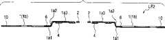
在该公开中公布的具有LOC结构的叠置半导体器件包括:一个树脂体;第一和第二半导体芯片,它们位于树脂体之内并具有形成在作为上和下表面(一个主表面和与其相对的另一主表面)中的上表面(即一个主表面)的电路形成表面上的电极;一个第一引线,它在树脂体之内和之外延伸并经过一个绝缘膜而被接合到第一半导体芯片的电路形成表面上;以及,一个第二引线,它位于树脂体之内和之外,并经过一个绝缘膜而被接合到第二半导体芯片的电路形成表面上,并借助一个导电连线而与电路形成表面的电极相电连接。The stacked semiconductor device with the LOC structure disclosed in this publication includes: a resin body; first and second semiconductor chips located inside the resin body and having surfaces formed as upper and lower surfaces (one main surface and The electrode on the circuit-forming surface of the upper surface (that is, one main surface) in the other main surface of the other main surface); a first lead, which extends inside and outside the resin body and is bonded to the first through an insulating film; on the circuit-forming surface of the semiconductor chip; and, a second lead, which is located inside and outside the resin body, and bonded to the circuit-forming surface of the second semiconductor chip through an insulating film, and via a conductive wiring Instead, it is electrically connected to the electrodes on the circuit-forming surface.
第一半导体芯片和第二半导体芯片都得到叠置,从而使它们的电路形成表面彼此相隔一个预定的间隙而相对。第一引线和第二引线被叠置,从而使每一个的一部分相重叠,并通过激光焊接而电和机械连接。Both the first semiconductor chip and the second semiconductor chip are stacked so that their circuit-forming surfaces are opposed to each other with a predetermined gap therebetween. The first lead and the second lead are superimposed such that a portion of each overlaps, and are electrically and mechanically connected by laser welding.
第一引线包括:位于树脂体之内的一个内引线部分,它在第一半导体芯片的电路形成表面的一侧上延伸并在第一半导体芯片的电路形成表面上延伸;以及,一个弯曲成J形引线的外引线部分,它是一种表面安装封装。The first lead includes: an inner lead portion located inside the resin body, extending on the side of the circuit forming surface of the first semiconductor chip and extending on the circuit forming surface of the first semiconductor chip; The outer lead part of the shaped lead, it is a surface mount package.
这种第一引线的内引线部分被弯曲,从而使经过一个绝缘膜与第一半导体芯片的电路形成表面接合的部分比在第一半导体芯片的一侧上延伸的部分更接近芯片的电路形成表面。The inner lead portion of this first lead is bent so that the portion bonded to the circuit forming surface of the first semiconductor chip through an insulating film is closer to the circuit forming surface of the chip than the portion extending on one side of the first semiconductor chip .
第二引线在第二半导体芯片的电路形成表面的一侧上延伸,并在第二半导体芯片的电路形成表面上延伸。这种引线被弯曲,从而使经过一个绝缘膜而接合到第二半导体芯片的电路形成表面上的部分比在第二半导体芯片的一侧上延伸的部分更接近芯片的电路形成表面。The second lead extends on one side of the circuit formation surface of the second semiconductor chip, and extends on the circuit formation surface of the second semiconductor chip. Such leads are bent so that the portion bonded to the circuit formation surface of the second semiconductor chip via an insulating film is closer to the circuit formation surface of the chip than the portion extending on one side of the second semiconductor chip.
在激光焊接之后,与第二半导体芯片相连的第二引线的另一端在模转移步骤之前在树脂体之内被切断,因而它不被从树脂体拉出。换言之,被拉出树脂体的外引线被用作了两个半导体芯片的公共外连接端。After the laser welding, the other end of the second lead connected to the second semiconductor chip is cut inside the resin body before the die transfer step so that it is not pulled out from the resin body. In other words, the external leads drawn out of the resin body are used as common external connection terminals of the two semiconductor chips.
根据上述树脂模制型半导体器件,形成一个存储器LSI的两个半导体芯片可借助树脂被封闭在一个薄封装中,因而能够在与包括一个树脂封闭的半导体芯片的封装相同的尺寸上实现两倍的存储容量。According to the above-mentioned resin molded type semiconductor device, two semiconductor chips forming one memory LSI can be enclosed in a thin package by means of resin, thereby enabling to achieve twice the size of a package including one resin-enclosed semiconductor chip. storage capacity.
本发明人开发的,是一种新的具有适合于更薄组装的LOC结构的叠置半导体器件。这种叠置半导体器件还没有被公布,然而,它具有如在本申请人早些时候递交的美国申请序号09/161,725号(1998年9月29日递交)中描述的以下结构。What the present inventors have developed is a novel stacked semiconductor device having an LOC structure suitable for thinner packaging. Such a stacked semiconductor device has not been published yet, however, it has the following structure as described in US Application Serial No. 09/161,725 (filed September 29, 1998) filed earlier by the present applicant.
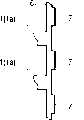
该器件主要包括:一个树脂体;设置在树脂体之内的一个第一和第二半导体芯片,它们具有形成在作为上和下表面中的上表面(即一个主表面)的电路形成表面上的电极;一个第一引线,它在树脂体之内和之外延伸,并经过一个绝缘膜而被接合到第一半导体芯片的电路形成表面上,并通过一个导线而与电路形成表面的电极电连接;以及,一个第二引线,它在树脂体之内和之外延伸,经过一个绝缘膜而接合到第二半导体芯片的电路形成表面上,并通过一个导线而与电路形成表面的电极电连接。The device mainly includes: a resin body; a first and a second semiconductor chip provided inside the resin body, which have a circuit forming surface formed on an upper surface (i.e., a main surface) as an upper surface (ie, a main surface) among the upper and lower surfaces. Electrode; a first lead extending inside and outside the resin body, bonded to the circuit forming surface of the first semiconductor chip through an insulating film, and electrically connected to the electrode of the circuit forming surface through a wire and, a second lead extending inside and outside the resin body, bonded to the circuit forming surface of the second semiconductor chip through an insulating film, and electrically connected to electrodes of the circuit forming surface through a wire.
本发明的叠置半导体器件可以是例如一种TSOP(薄的小轮廓封装)。两个半导体芯片即第一和第二半导体芯片—它们形成了具有相同的存储容量(例如64Mbyte DRAM)的存储LSI-在用转移模制方法形成的封装件(树脂体)之内彼此叠置,并在它们的下表面(即一个主表面和对着它的另一个主表面)接触的情况下得到封闭。The stacked semiconductor device of the present invention may be, for example, a TSOP (Thin Small Outline Package). Two semiconductor chips, that is, first and second semiconductor chips, which form a storage LSI having the same storage capacity (for example, 64Mbyte DRAM) are stacked on each other within a package (resin body) formed by a transfer molding method, and are closed with their lower surfaces (ie one major surface and the other major surface facing it) in contact.
第一引线和第二引线得到叠置,从而使每一个的一部分相重叠,并通过激光焊接而电和机械连接。The first lead and the second lead are superimposed such that a portion of each overlaps, and are electrically and mechanically connected by laser welding.
第一引线和第二引线每一个都包括位于树脂体之内的一个内引线部分和位于树脂体之外的一个外引线部分。第一和第二半导体芯片的内引线部分包括:一个第一部分,它在半导体芯片(在第一引线的情况下为第一半导体芯片且在第二引线的情况下为第二半导体芯片)的电路形成表面的一侧上延伸,并在半导体芯片的电路形成表面上延伸;一个第二部分,它从第一部分向着半导体芯片的下表面弯曲;以及,一个第三部分,它沿着与第一部分相同的方向从第二部分弯曲。第一引线和第二引线的第三部分在树脂体之内和之外延伸,并沿着上/下方向彼此叠置。第一引线的外引线部分被弯曲成鸥翅形引线,它是一种表面安装封装件。第二引线的外引线部分的长度比第一引线的外引线部分的长度短。Each of the first lead and the second lead includes an inner lead portion located inside the resin body and an outer lead portion located outside the resin body. The inner lead parts of the first and second semiconductor chips include: a first part which is connected to the circuit of the semiconductor chip (the first semiconductor chip in the case of the first lead and the second semiconductor chip in the case of the second lead) extending on one side of the forming surface and extending over the circuit forming surface of the semiconductor chip; a second portion which is bent from the first portion toward the lower surface of the semiconductor chip; and, a third portion which is along the same The direction of is bent from the second part. Third portions of the first lead and the second lead extend inside and outside the resin body, and overlap each other in an up/down direction. The outer lead portion of the first lead is bent into a gull-wing lead, which is a surface mount package. The length of the outer lead portion of the second lead is shorter than the length of the outer lead portion of the first lead.
因此,在上述叠置半导体器件中,与其中两个半导体芯片的元件形成表面彼此相对地设置且内引线部分被设置在两者之间的间隙中的上述公开的叠置半导体器件不同,两个半导体芯片的下表面彼此接触。Therefore, in the above-mentioned stacked semiconductor device, unlike the above-disclosed stacked semiconductor device in which the element forming surfaces of the two semiconductor chips are disposed opposite to each other and the inner lead portion is disposed in the gap therebetween, the two The lower surfaces of the semiconductor chips are in contact with each other.
因而在两个半导体芯片没有间隙,且树脂体的厚度可以相应地变得更薄。There is thus no gap between the two semiconductor chips, and the thickness of the resin body can be made thinner accordingly.
换言之,由于在第一半导体芯片与第二半导体芯片之间没有第一引线或第二引线,两个半导体芯片之间的空间可以比现有技术中叠置半导体器件的其中第一引线和第二引线被分别设置在第一半导体芯片与第二半导体芯片之间的情况更窄。因此,树脂体的厚度能够得到减小,且叠置的半导体器件可以作得更窄。In other words, since there is no first lead or second lead between the first semiconductor chip and the second semiconductor chip, the space between the two semiconductor chips can be larger than that of the prior art in which the first lead and the second lead are stacked. The case where the leads are respectively provided between the first semiconductor chip and the second semiconductor chip is narrower. Therefore, the thickness of the resin body can be reduced, and the stacked semiconductor device can be made narrower.
至于半导体芯片与引线之间的浮动电容,设置在第一半导体芯片的元件形成表面上的引线与第二半导体芯片之间的浮动电容,以及设置在第二半导体芯片的元件形成表面上的引线与第一半导体芯片的浮动电容,都可以被消除,因而加到引线上的浮动电容被相应地减小,且引线的信号传播延迟得到了改善。As for the floating capacitance between the semiconductor chip and the lead, the floating capacitance between the lead provided on the element forming surface of the first semiconductor chip and the second semiconductor chip, and the lead provided on the element forming surface of the second semiconductor chip and the The floating capacitance of the first semiconductor chip can be eliminated, so that the floating capacitance added to the leads is correspondingly reduced, and the signal propagation delay of the leads is improved.
换言之,由于没有在第一半导体芯片与第二半导体芯片之间的第一引线和第二引线,在加到第一引线上的浮动电容(芯片/引线电容)中,第二半导体芯片产生的浮动电容,与现有技术的叠置半导体器件的其中第一引线和第二引线被设置在第一半导体芯片和第二半导体芯片之间的情况相比,得到了有效的消除;且加到第二引线上的浮动电容(芯片/引线电容)中,第一半导体芯片产生的浮动电容得到了有效的减小。因此,加到引线即第一引线和第二引线上的浮动电容得到了减小。结果,引线的信号传播延迟得到了改善,且叠置的半导体器件的电特性得到了增强。In other words, since there are no first lead and second lead between the first semiconductor chip and the second semiconductor chip, in the floating capacitance (chip/lead capacitance) added to the first lead, the floating caused by the second semiconductor chip Capacitance, compared with the case where the first lead and the second lead are arranged between the first semiconductor chip and the second semiconductor chip of the stacked semiconductor device of the prior art, has been effectively eliminated; and added to the second Of the floating capacitance on the lead (chip/lead capacitance), the floating capacitance generated by the first semiconductor chip is effectively reduced. Therefore, the floating capacitance added to the leads, ie, the first lead and the second lead, is reduced. As a result, the signal propagation delay of the leads is improved, and the electrical characteristics of the stacked semiconductor device are enhanced.
第一半导体芯片由第一引线框的引线所固定的树脂封闭,且第二半导体芯片由借助第二引线框的引线固定的树脂体封闭。换言之,这种树脂封闭的半导体器件是利用两个引线框产生的。在这两个引线框中,其中的一个没有外引线部分且只有内引线部分。换言之,在这种树脂封闭半导体器件中,从树脂体拉出的另一引线框的外引线部分被用作两个半导体芯片的公共外部连接端。The first semiconductor chip is enclosed by a resin fixed by the leads of the first lead frame, and the second semiconductor chip is enclosed by the resin body fixed by the leads of the second lead frame. In other words, this resin-sealed semiconductor device is produced using two lead frames. Of the two lead frames, one of them has no outer lead parts and only inner lead parts. In other words, in this resin-enclosed semiconductor device, the outer lead portion of the other lead frame pulled out from the resin body is used as a common external connection terminal for two semiconductor chips.
在用于制作这种树脂封闭半导体器件的步骤中,第一引线框的引线的内引线部分首先被接合到第一半导体芯片的元件形成表面上,且第二引线框的引线的内引线部分被接合到第二半导体芯片的元件形成表面上。In the steps for producing such a resin-enclosed semiconductor device, the inner lead portions of the leads of the first lead frame are first bonded to the element forming surface of the first semiconductor chip, and the inner lead portions of the leads of the second lead frame are bonded Bonded to the element formation surface of the second semiconductor chip.
随后,第一引线框的引线的内引线部分和形成在第一半导体芯片的元件形成表面上的一个接合台借助连线而得到连接,第二引线框的引线的内引线部分和形成在第二半导体芯片的元件形成表面上的一个接合台借助连线而得到连接,这两个引线框被叠置,从而使第一半导体芯片的下表面和第二半导体芯片的下表面彼此相对,这些引线框被压入一个模中,且第一半导体芯片和第二半导体芯片借助树脂而得到封闭。Subsequently, the inner lead portion of the lead of the first lead frame and a bonding pad formed on the element forming surface of the first semiconductor chip are connected by wires, and the inner lead portion of the lead of the second lead frame and a bonding pad formed on the second semiconductor chip are connected by wires. A bonding stage on the element forming surface of the semiconductor chip is connected by a wire, and the two lead frames are stacked so that the lower surface of the first semiconductor chip and the lower surface of the second semiconductor chip are opposed to each other, and the lead frames are pressed into a mold, and the first semiconductor chip and the second semiconductor chip are sealed with resin.
随后,在封装件(树脂体)之外延伸的一个第一引线框阻挡杆和一个第二引线框阻挡杆,利用一个切割模,而得到切割,从而形成了一个引线框的外引线部分。Subsequently, a first lead frame stop bar and a second lead frame stop bar extending outside the package (resin body) are cut using a cutting die, thereby forming an outer lead portion of a lead frame.
根据上述制作方法,两个引线框的切割能够在一个步骤中进行,因而与其中一个引线框的外引线部分在模制步骤之前得到切割的上述公布中的封装件制作方法相比,加工过程得到了缩短。According to the above manufacturing method, the cutting of the two lead frames can be performed in one step, and thus the process is improved compared to the package manufacturing method in the above publication in which the outer lead portion of one lead frame is cut before the molding step. shortened.
(1)然而,在上述制作方法中,载有半导体芯片的两个引线框得到叠置,被插入一个模中,且树脂被注入模腔中且一个引线框阻挡杆和另一个引线框阻挡杆被一个上夹持表面和一个下夹持表面沿着上/下方向所夹持。如果上和下模夹持表面没有以足够的力夹紧阻挡杆,阻挡杆之一就可能由于内部压力而向着腔外移动,树脂可能通过此时在一个阻挡杆与另一阻挡杆之间产生的间隙而泄漏到腔之外,且这可能引起模制的缺陷。(1) However, in the above manufacturing method, two lead frames carrying semiconductor chips are stacked, inserted into one mold, and resin is injected into the cavity and one lead frame stopper bar and the other lead frame stopper bar Clamped in up/down direction by an upper clamping surface and a lower clamping surface. If the clamping surfaces of the upper and lower molds do not clamp the blocking rods with sufficient force, one of the blocking rods may move toward the outside of the cavity due to internal pressure, and resin may pass between one blocking rod and the other blocking rod at this time. The gap leaks out of the cavity, and this may cause molding defects.
具体地,在近来的LSI引线框中,随着引线的间距和宽度减小,阻挡杆的宽度也变窄。结果,难于保证模与阻挡杆的夹持表面之间有足够的接触面积,因而阻挡杆上的夹持表面的夹紧力不够,且阻挡杆会由于树脂注入压力而移动。Specifically, in recent LSI lead frames, as the pitch and width of the leads are reduced, the width of the barrier bars is also narrowed. As a result, it is difficult to secure a sufficient contact area between the mold and the clamping surface of the barrier bar, so the clamping force of the clamping surface on the barrier bar is insufficient, and the barrier bar moves due to resin injection pressure.
处理这种问题的一种方式,是增大引线框的阻挡杆的宽度,但如果在其中两个叠置阻挡杆被同时切割的上述制作过程中这样做,加在切割模上的负荷增大,从而其寿命缩短。One way to deal with this problem is to increase the width of the barrier bar of the lead frame, but if this is done in the above-mentioned manufacturing process in which two stacked barrier bars are cut simultaneously, the load on the cutting die increases , thereby shortening its lifespan.
进一步地,本发明人在开发上述叠置的半导体器件的过程中发现了其他的问题。Further, the present inventors discovered other problems during the development of the above-mentioned stacked semiconductor device.
(2)这种叠置的半导体器件是借助采用两个引线框的组装过程而制成的,因而需要接合在第二引线框支撑的第二引线和第一引线框中支撑的第一引线适合于微组装的激光焊接可有效地被用于接合第一和第二引线,然而如果激光焊接是在树脂封闭体形成之前的阶段进行,就会产生以下问题。(2) Such a stacked semiconductor device is manufactured by an assembly process using two lead frames, so it is necessary to bond the second lead supported in the second lead frame and the first lead supported in the first lead frame to suit Laser welding for micro-assembly can be effectively used to join the first and second leads, however if the laser welding is performed at a stage before the resin enclosure is formed, the following problems arise.
在激光焊接中,引线的接合部分(焊接部分)受到激光照射并熔化,因而大量的熔化材料通过激光照射而扩散到了周围的区域。由于第一半导体芯片和第二半导体芯片以它们的下表面彼此相对的方式得到叠置,由于这种熔化而产生的扩散的材料飞到半导体芯片的电路形成表面上。In laser welding, the bonding portion (welding portion) of the lead wire is irradiated with laser light and melted, so that a large amount of molten material is diffused to the surrounding area by the laser irradiation. Since the first semiconductor chip and the second semiconductor chip are stacked with their lower surfaces facing each other, the diffused material due to this melting flies onto the circuit formation surface of the semiconductor chip.
当扩散材料飞到半导体芯片的电路形成表面上时,由于这种材料是高温的,它对形成在半导体芯片的电路形成表面上的保护膜造成了热损坏,因而保护膜之下的互连经常断开或与相邻的互连发生短路。如果发生了大量的这种缺陷,半导体芯片会损坏,且叠置的半导体器件的产量(yield)就会有严重的下降。特别地,在其中保护膜是用聚酰胺树脂(polyimide resin)制成以改善与树脂封闭体的树脂的附着特性或DRAM的抗α射线特性的半导体芯片中,由于扩散材料的缺陷是很容易发生的。When the diffusion material flies onto the circuit formation surface of the semiconductor chip, since this material is high temperature, it causes thermal damage to the protective film formed on the circuit formation surface of the semiconductor chip, so that the interconnection under the protective film is often open or short circuit to an adjacent interconnection. If a large number of such defects occur, the semiconductor chip is damaged, and the yield of the stacked semiconductor device is seriously lowered. Particularly, in a semiconductor chip in which the protective film is made of polyimide resin to improve the adhesion characteristics with the resin of the resin enclosure or the anti-α ray characteristics of the DRAM, defects due to the diffusion material are likely to occur of.
进一步地,由于引线的接合部分是通过激光焊接熔化的,包含在引线中的杂质(例如硫)变成了外部气体附着在半导体芯片表面上,并产生化学反应而引起芯片表面的恶化。如果发生了半导体芯片表面的恶化,半导体芯片与树脂体的树脂之间的附着显著地降低,且在两者之间的界面处由于热膨胀系数差造成的热应力而容易发生剥离。如果发生了这种界面剥离,包含在树脂体的树脂中的水份就在剥离区中累积,且累积的水份会在加热循环测试(它是在产品完成之后进行的环境测试)期间或者由于芯片被焊接到电路板上时由于回流焊接加热而蒸发。这使树脂体发生裂缝,并引起叠置的半导体器件的可靠性的下降。Further, since the bonding portion of the wire is melted by laser welding, impurities such as sulfur contained in the wire become external gas and adhere to the surface of the semiconductor chip and cause a chemical reaction to cause deterioration of the chip surface. If deterioration of the surface of the semiconductor chip occurs, the adhesion between the semiconductor chip and the resin of the resin body is remarkably reduced, and peeling easily occurs at the interface therebetween due to thermal stress due to the difference in thermal expansion coefficient. If such interfacial peeling occurs, the moisture contained in the resin of the resin body accumulates in the peeled area, and the accumulated moisture may occur during the heat cycle test (which is an environmental test performed after the product is completed) or due to When the chip is soldered to the circuit board, it evaporates due to the heat of reflow soldering. This causes cracks in the resin body and causes a decrease in the reliability of the stacked semiconductor device.
进一步地,引线框倾向于随着引线的变细而变薄,且更容易由于不够的机械强度而发生引线的弯曲。如果引线发生弯曲,在第一引线的接合部与第二引线的接合部之间将出现一个间隙,从而造成焊接缺陷。结果,第一引线和第二引线必须借助固定工具进行限制,从而叠置的半导体器件的产量下降。Further, the lead frame tends to become thinner as the leads become thinner, and bending of the leads more easily occurs due to insufficient mechanical strength. If the leads are bent, a gap will appear between the bonded portion of the first lead and the bonded portion of the second lead, resulting in a soldering defect. As a result, the first lead and the second lead must be restrained by means of a fixing tool, so that the yield of the stacked semiconductor device decreases.
(3)在叠置的半导体器件以及通常的半导体器件中,为了在安装期间保持焊接泄漏特性并改善抗腐蚀特性,必须在外引线上电镀导电膜(电镀膜),该膜包括例如铅-锡。这种电镀是通常的电镀,包括预处理—诸如去油步骤、水洗步骤、抛光步骤和水洗步骤,以及后处理—诸如电镀步骤、水洗步骤、中和步骤、热水洗步骤、以及干燥步骤。当进行包括这些步骤的电镀时,在叠置的半导体器件中,电镀是用重叠的两个引线框进行的。因此,前面的阶段的某些处理液(反应剂)由于毛细作用而被留在了第一引线框与第二引线框之间,且来自前面阶段的大量的处理液可能被携带到随后的阶段处理液中。这种前面阶段的处理液的携带造成电镀缺陷,并大大降低了叠置的半导体器件的产量。另外,随后阶段的处理液必须频繁地更换,且叠置的半导体器件的产量降低。(3) In stacked semiconductor devices as well as conventional semiconductor devices, in order to maintain solder leakage characteristics and improve corrosion resistance during mounting, it is necessary to plate a conductive film (plating film) including, for example, lead-tin on the outer leads. This plating is usual plating, including pretreatments such as degreasing steps, water washing steps, polishing steps, and water washing steps, and postprocessing such as plating steps, water washing steps, neutralization steps, hot water washing steps, and drying steps. When electroplating including these steps is performed, in a stacked semiconductor device, electroplating is performed with two lead frames overlapped. Therefore, some process liquid (reactant) of the previous stage is retained between the first lead frame and the second lead frame due to capillary action, and a large amount of process liquid from the previous stage may be carried over to the subsequent stage in the treatment solution. This entrainment of the treatment liquid from the previous stage causes plating defects and greatly reduces the yield of stacked semiconductor devices. In addition, the treatment liquid at the subsequent stage must be frequently replaced, and the yield of stacked semiconductor devices decreases.
(4)在叠置的半导体器件中,树脂封闭体是由重叠的两个引线框形成的。用于支持引线框中的树脂体的后引线也被形成在两个引线框的每一个中相互重叠的位置处。(4) In the stacked semiconductor device, the resin enclosure is formed by overlapping two lead frames. Rear leads for supporting the resin bodies in the lead frames are also formed at positions overlapping each other in each of the two lead frames.
因此,在树脂体内后引线有两个相邻的表面,且由于这两个后引线是在进行了电镀之后从引线框的框体切割的,相邻引线的端部从树脂体暴露。如果这些相邻表面被暴露,来自外界的水份容易通过表面而穿入体的内部,且容易腐蚀半导体芯片的导线与电极之间的连接部分,以及内引线部分与引线和导线之间的连接部分。这引起了叠置的半导体芯片的可靠性的降低。Therefore, the rear leads have two adjacent surfaces in the resin body, and since the two rear leads are cut from the frame body of the lead frame after plating has been performed, the ends of the adjacent leads are exposed from the resin body. If these adjacent surfaces are exposed, moisture from the outside easily penetrates into the interior of the body through the surface, and easily corrodes the connection part between the wire and the electrode of the semiconductor chip, and the connection between the inner lead part and the lead wire and the wire part. This causes a reduction in the reliability of the stacked semiconductor chips.
(5)叠置的半导体器件是借助采用两个引线框的组装处理而产生的。在第一引线框中,第一引线的外引线部分的端部被支撑在框体中,且第一引线的中间部分被阻挡杆互连并被阻挡杆支撑在框体中。在第二引线框中,第二引线的外引线部分的端部借助阻挡杆互连,并被阻挡杆支撑在框体中。换言之,在第二引线框中,在阻挡杆与框体限定的区域中没有受到支撑的部件,因而刚性低且容易发生弯曲。因此,当在把第二引线的内引线部分固定到半导体芯片的电路形成表面之后的随后阶段的一个步骤中第二引线框得到转移时,芯片会摇摆且容易从第二引线框落下,因而叠置的半导体器件的产量下降。(5) A stacked semiconductor device is produced by an assembly process using two lead frames. In the first lead frame, ends of outer lead portions of the first leads are supported in the frame body, and intermediate portions of the first leads are interconnected by blocking bars and supported in the frame body by the blocking bars. In the second lead frame, ends of the outer lead portions of the second leads are interconnected by means of barrier bars, and are supported in the frame body by the barrier bars. In other words, in the second lead frame, there is no supported part in the area defined by the barrier bar and the frame body, so the rigidity is low and bending is easy to occur. Therefore, when the second lead frame is transferred in a step of a subsequent stage after the inner lead portion of the second lead is fixed to the circuit-forming surface of the semiconductor chip, the chip is shaken and easily dropped from the second lead frame, so that the stack The output of semiconductor devices that are set to decline.
(6)在叠置的半导体器件中,树脂封闭体是借助适合于大规模生产的转移模制方法形成的。这种转移模制方法是一种用于通过把树脂压注到模腔中而形成一个树脂体的方法。树脂通常是包含大量的填充物的环氧加热固化树脂,以实现较低的应力。(6) In the stacked semiconductor device, the resin enclosure is formed by transfer molding suitable for mass production. This transfer molding method is a method for forming a resin body by injecting resin into a cavity. The resin is usually an epoxy heat cure resin containing a large amount of filler to achieve lower stress.
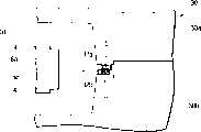
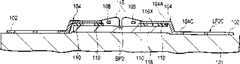
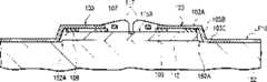
半导体芯片主要包括:一个半导体衬底;在该半导体衬底的一个电路形成表面上的一个绝缘层;一个多层互连层,包括多个彼此叠置的互连层;以及,一个表面保护膜(最后保护膜),用于掩盖这种多层互连层,因而半导体芯片沿着芯片的下表面向外凸起的方向弯曲。如果两个半导体芯片在此状态下以它们的下表面彼此相对的方式叠置在一起,在两个半导体芯片71之间将形成一个间隙72,该间隙一般从两个半导体芯片71的中心向着边缘变宽,如图32所示。The semiconductor chip mainly includes: a semiconductor substrate; an insulating layer on a circuit-forming surface of the semiconductor substrate; a multilayer interconnection layer including a plurality of interconnection layers stacked on each other; and, a surface protection film (final protective film) for masking such a multi-layer interconnection layer so that the semiconductor chip is bent outwardly along the lower surface of the chip. If two semiconductor chips are stacked together with their lower surfaces facing each other in this state, a gap 72 will be formed between the two semiconductor chips 71, and the gap generally extends from the center of the two semiconductor chips 71 toward the edges. Widen, as shown in Figure 32.
因此,当两个半导体芯片71被设置在模75的腔76中,且树脂77被压力注入到腔76中以形成图33显示的树脂体时,树脂77通过两个半导体芯片71之间的间隙而渗透出来。然而,由于树脂77包含混合到其中的填充物,它不能透过比填充物的晶粒直径小的间隙,因而在两个半导体芯片71之间形成了一个空间78。如果在两个半导体芯片71之间形成了这样一个空间78,当在至腔76的树脂注入完成之后把高于注入压强的压强用来除去包括在树脂中的气泡时,在半导体芯片71中将产生从空间78向外辐射的裂缝,且这将造成叠置的半导体器件的产量的下降。Therefore, when two semiconductor chips 71 are set in the cavity 76 of the mold 75, and the resin 77 is pressure-injected into the cavity 76 to form the resin body shown in FIG. 33, the resin 77 passes through the gap between the two semiconductor chips 71. And seep out. However, since the resin 77 contains a filler mixed therein, it cannot penetrate a gap smaller than the grain diameter of the filler, thereby forming a space 78 between the two semiconductor chips 71 . If such a space 78 is formed between the two semiconductor chips 71, when a pressure higher than the injection pressure is used to remove air bubbles included in the resin after the resin injection to the cavity 76 is completed, the semiconductor chips 71 will Cracks radiating outward from the space 78 are generated, and this will cause a decrease in the yield of the stacked semiconductor device.
因而本发明的目的,是提供一种能够改善半导体器件的产量的技术。It is therefore an object of the present invention to provide a technique capable of improving the yield of semiconductor devices.
本发明的另一个目的,是提供一种能够改善半导体器件的生产率(productivity)的技术。Another object of the present invention is to provide a technique capable of improving the productivity of semiconductor devices.
本发明的再一个目的,是提供一种能够改善半导体器件的可靠性的技术。Still another object of the present invention is to provide a technique capable of improving the reliability of semiconductor devices.
本发明的再一个目的,是提供一种技术,它能够在其中利用两个引线框而对两个半导体芯片进行树脂封闭的半导体器件生产中防止阻挡杆由于模制期间树脂注入压强而发生移动。Still another object of the present invention is to provide a technique capable of preventing movement of barrier bars due to resin injection pressure during molding in the production of a semiconductor device in which two semiconductor chips are resin-encapsulated using two lead frames.
通过以下的详细描述和附图,本发明的这些和其他的目的和新颖特征将变得显而易见。These and other objects and novel features of the present invention will become apparent from the following detailed description and accompanying drawings.
现在简要描述本申请中公布的本发明的基本特征。The essential features of the invention disclosed in this application will now be briefly described.
(1)在根据本发明的半导体器件中,第一半导体芯片的下表面和第二半导体芯片的下表面被封闭在一个封装件中,其中固定在第一半导体芯片的元件形成表面上的第一引线框的多个引线的内引线部分和形成在第一半导体芯片的元件形成表面上的一个接合台,以及固定在第二半导体芯片的元件形成表面上的一个第二引线框的多个引线的内引线部分和形成在第二半导体芯片的元件形成表面上的一个接合台,分别得到电连接,且暴露于封装件之外的第二引线框的阻挡杆的宽度小于暴露在封装件之外的第一引线框的一个阻挡杆的宽度。(1) In the semiconductor device according to the present invention, the lower surface of the first semiconductor chip and the lower surface of the second semiconductor chip are enclosed in a package in which the first semiconductor chip fixed on the element forming surface of the first semiconductor chip Inner lead parts of the plurality of leads of the lead frame and a bonding stage formed on the element forming surface of the first semiconductor chip, and the plurality of leads of a second lead frame fixed on the element forming surface of the second semiconductor chip The inner lead portion and a bonding pad formed on the element forming surface of the second semiconductor chip are respectively electrically connected, and the width of the stop bar of the second lead frame exposed outside the package is smaller than that of the second lead frame exposed outside the package. The width of one barrier bar of the first leadframe.
(2)根据本发明的半导体器件的生产方法包括以下步骤(a)-(d):(2) The production method of the semiconductor device according to the present invention comprises the following steps (a)-(d):
(a)提供一个第一引线框,它包括借助一个第一阻挡杆而互连的多个引线,以及(a) providing a first leadframe comprising a plurality of leads interconnected by a first barrier bar, and
提供一个第二引线框,它包括借助一个第二阻挡杆而互连的多个引线,其中在第二阻挡杆上形成有一个沿着宽度方向延伸的虚设引线,providing a second lead frame comprising a plurality of leads interconnected by a second barrier bar on which a dummy lead extending in a width direction is formed,
(b)把第一引线框的一个引线的一个内引线部分固定在第一半导体芯片的一个元件形成表面上,并把第二引线框的一个引线的一个内引线部分固定在第二半导体芯片的元件形成表面上,(b) fixing an inner lead portion of a lead of the first lead frame to an element forming surface of the first semiconductor chip, and fixing an inner lead portion of a lead of the second lead frame to an element forming surface of the second semiconductor chip element formed on the surface,
(c)把第一引线框的一个引线的内引线部分与形成在第一半导体芯片的元件形成表面上的一个接合台电连接,并把第二引线框的引线的内引线部分与形成在第二半导体芯片的元件形成表面上的一个接合台电连接,(c) Electrically connecting an inner lead portion of a lead of the first lead frame to a bonding pad formed on the element formation surface of the first semiconductor chip, and connecting an inner lead portion of a lead of the second lead frame to a bonding pad formed on the second semiconductor chip. The components of the semiconductor chip form an electrical connection at a bonding pad on the surface,
(d)把第一半导体芯片和第二半导体芯片封闭在封装件中并使第一引线框与第二引线框重叠从而使第一半导体芯片的下表面和第二半导体芯片的下表面彼此相对,以及(d) enclosing the first semiconductor chip and the second semiconductor chip in the package and overlapping the first lead frame with the second lead frame so that the lower surface of the first semiconductor chip and the lower surface of the second semiconductor chip are opposed to each other, as well as
(e)切断第一引线框的第一阻挡杆并切断第二引线框暴露在封装件之外的第二阻挡杆。(e) Cutting off the first barrier bar of the first lead frame and cutting the second barrier bar of the second lead frame exposed outside the package.
(3)在包括一个树脂体、置于树脂封闭体之内并具有形成在上和下表面中的上表面上的电极的第一半导体芯片和第二半导体芯片、在树脂体之内和之外延伸并与第一半导体芯片的电极电连接的一个第一引线、以及在树脂体之内和之外延伸并与第二半导体芯片的电极电连接的一个第二引线的半导体器件的生产方法中,第一引线和第二引线在形成树脂体之后通过焊接而接合,且第一引线与第二引线的焊接部分相重叠。(3) In the first semiconductor chip and the second semiconductor chip comprising a resin body placed inside the resin enclosure and having electrodes on the upper surface formed in the upper and lower surfaces, inside and outside the resin body In the production method of a semiconductor device of a first lead extending and electrically connected to an electrode of a first semiconductor chip, and a second lead extending inside and outside of a resin body and electrically connecting to an electrode of a second semiconductor chip, The first lead and the second lead are bonded by welding after forming the resin body, and the welded portion of the first lead and the second lead overlap.
这种焊接是借助第一引线或第二引线之上的激光进行的。This welding is performed by means of a laser over the first lead or the second lead.
(4)在包括封闭支撑在第一引线框的框体中的第一引线的内引线部分、支撑在第二引线框的框体中的第二引线的内引线部分、接合在第一引线的内引线部分上并具有与第一引线的内引线部分电连接的一个电极的第一半导体芯片、以及接合到第二引线的内引线部分上并具有与第二引线的内引线部分电连接的一个电极的第二半导体芯片的步骤,并进一步包括对第一引线和第二引线的外引线部分进行电镀的步骤的一种半导体器件的制作方法方法中,(4) In the inner lead part comprising the first lead closed and supported in the frame body of the first lead frame, the inner lead part of the second lead supported in the frame body of the second lead frame, the inner lead part bonded to the first lead A first semiconductor chip on the inner lead part and having one electrode electrically connected to the inner lead part of the first lead, and a first semiconductor chip bonded to the inner lead part of the second lead and having an electrode electrically connected to the inner lead part of the second lead In the step of the electrode of the second semiconductor chip, and further including the step of electroplating the outer lead part of the first lead and the second lead, in a method for manufacturing a semiconductor device,
第二引线框的框体在用树脂进行封闭之后并在电镀之前被除去。The frame body of the second lead frame is removed after sealing with resin and before plating.
(5)半导体器件的制作方法包括以下步骤:(5) The manufacturing method of the semiconductor device comprises the following steps:
制备具有形成在上和下表面中的上表面上的电极的第一半导体芯片和第二半导体芯片,preparing a first semiconductor chip and a second semiconductor chip having electrodes formed on the upper surface of the upper and lower surfaces,
制备包括位于第一框体围绕的一个区中的多个第一引线的第一引线框,其中外引线部分的端部位于第一框体中,且中间部分借助第一阻挡杆而互连并借助第一阻挡杆而被支撑在第一框体中,并包括位于被第一框体围绕的一个区中并被支撑在第一框体中的一个后引线,制备一个包括位于被第二框体所围绕的一个区中的多个第二引线的第二引线框,其中外引线部分的端部借助第二阻挡杆而互连并被第二阻挡杆支撑在第二框体中,preparing a first lead frame including a plurality of first leads located in a region surrounded by a first frame body, wherein ends of outer lead portions are located in the first frame body, and intermediate portions are interconnected by means of first barrier bars and being supported in the first frame by means of the first blocking bar, and comprising a rear lead located in a region surrounded by the first frame and supported in the first frame, preparing a rear lead comprising a region surrounded by the second frame a second lead frame of a plurality of second leads in a region surrounded by the body, wherein the ends of the outer lead parts are interconnected by means of second barrier bars and are supported in the second frame body by the second barrier bars,
把第一引线的内引线部分接合到第一半导体芯片的上表面,并把第二引线的内引线部分接合到第二半导体芯片的上表面,bonding the inner lead portion of the first lead to the upper surface of the first semiconductor chip, and bonding the inner lead portion of the second lead to the upper surface of the second semiconductor chip,
借助一个导线把第一半导体芯片的一个电极电连接到第一引线的内引线部分,并借助一个导线把第二半导体芯片的一个电极电连接到第二引线的内引线部分,以及electrically connecting an electrode of the first semiconductor chip to the inner lead portion of the first lead by means of a wire, and electrically connecting an electrode of the second semiconductor chip to the inner lead portion of the second lead by means of a wire, and
借助一个树脂体,以使第一引线框和第二引线框重叠从而使第一半导体芯片和第二半导体芯片的下表面彼此相对的方式封闭第一半导体芯片、第二半导体芯片、第一引线的内引线部分、第二引线的内引线部分、第一导线、第二导线和后引线。By means of a resin body, the first semiconductor chip, the second semiconductor chip, and the first lead frame are closed in such a manner that the first lead frame and the second lead frame overlap so that the lower surfaces of the first semiconductor chip and the second semiconductor chip face each other. The inner lead portion, the inner lead portion of the second lead, the first lead, the second lead, and the rear lead.
(6)半导体器件的制作方法包括以下步骤:(6) The manufacturing method of the semiconductor device comprises the following steps:
制备具有形成在上和下表面中的上表面上的电极的第一半导体芯片和第二半导体芯片,preparing a first semiconductor chip and a second semiconductor chip having electrodes formed on the upper surface of the upper and lower surfaces,
制备包括位于第一框体围绕的一个区中的多个第一引线的第一引线框,其中外引线部分的端部位于第一框体中,且中间部分借助第一阻挡杆而互连并借助第一阻挡杆而被支撑在第一框体中,制备包括位于围绕在第二框体中的一个区中的多个第二引线的一个第二引线框,其中外引线部分的端部借助第二阻挡杆得到互连并被第二阻挡杆支撑在第二框体中,并包括位于第二框体所围绕的一个区中的一个加强引线,并被第二阻挡杆和第二框体所支撑,preparing a first lead frame including a plurality of first leads located in a region surrounded by a first frame body, wherein ends of outer lead portions are located in the first frame body, and intermediate portions are interconnected by means of first barrier bars and Supported in the first frame by means of the first barrier bar, a second lead frame comprising a plurality of second leads located in a region surrounded in the second frame is prepared, wherein the ends of the outer lead portions are The second blocking rods are interconnected and supported in the second frame by the second blocking rods, and include a reinforcing lead located in an area surrounded by the second frame, and are supported by the second blocking rods and the second frame supported by,
把第一引线的内引线部分接合到第一半导体芯片的上表面,以及bonding the inner lead portion of the first lead to the upper surface of the first semiconductor chip, and
把第二引线的内引线部分接合到第二半导体芯片的上表面,bonding the inner lead portion of the second lead to the upper surface of the second semiconductor chip,
借助一个导线把第一半导体芯片的一个电极电连接到第一引线的内引线部分,并借助一个导线把第二半导体芯片的一个电极与第二引线的内引线部分电连接,以及electrically connecting an electrode of the first semiconductor chip to the inner lead portion of the first lead by means of a wire, and electrically connecting an electrode of the second semiconductor chip to the inner lead portion of the second lead by means of a wire, and
借助一种树脂体,以使得第一引线框和第二引线框重叠从而使第一半导体芯片和第二半导体芯片的下表面彼此相对的方式,封闭第一半导体芯片、第二半导体芯片、第一引线的内引线部分、第二引线的内引线部分、第一导线和第二导线。By means of a resin body, the first semiconductor chip, the second semiconductor chip, the first The inner lead portion of the lead, the inner lead portion of the second lead, the first wire, and the second wire.
(7)在包括由大量的填充物形成的树脂体、具有形成在上和下表面中的上表面上的一个电极的第二半导体芯片和第一半导体芯片、在树脂体之内和之外延伸并与第一半导体芯片电连接的第一引线、在树脂体之内和之外延伸并电连接到第二半导体芯片的第二引线的半导体器件的制作方法中,第一半导体芯片和第二半导体芯片以使得它们的下表面彼此相对的方式叠置的半导体器件的制作方法中,(7) In the resin body formed of a large amount of filler, the second semiconductor chip and the first semiconductor chip having one electrode formed on the upper surface among the upper and lower surfaces, extending inside and outside the resin body In the manufacturing method of a semiconductor device comprising a first lead electrically connected to a first semiconductor chip and a second lead extending inside and outside a resin body and electrically connected to a second semiconductor chip, the first semiconductor chip and the second semiconductor chip In a method of manufacturing a semiconductor device in which chips are stacked such that their lower surfaces face each other,
第一半导体芯片、第二半导体芯片、第一引线的内引线部分、第二引线的内引线部分、第一导线和第二导线被设置在一个模的腔内,且在第一半导体芯片的下表面与第二半导体芯片的下表面之间填充有缓冲材料,且树脂被压注到该腔中以形成树脂体。The first semiconductor chip, the second semiconductor chip, the inner lead portion of the first lead, the inner lead portion of the second lead, the first wire and the second wire are arranged in a cavity of a mold, and under the first semiconductor chip A buffer material is filled between the surface and the lower surface of the second semiconductor chip, and resin is press-injected into the cavity to form a resin body.
(8)在包括由大量的填充物形成的树脂体、具有形成在上和下表面中的上表面上的一个电极的第二半导体芯片和第一半导体芯片、在树脂体之内和之外延伸并与第一半导体芯片电连接的第一引线、在树脂体之内和之外延伸并电连接到第二半导体芯片的第二引线的半导体器件的制作方法中,第一半导体芯片和第二半导体芯片以使得它们的下表面彼此相对的方式叠置的半导体器件的制作方法中,(8) In the second semiconductor chip and the first semiconductor chip comprising a resin body formed of a large amount of filler, having one electrode formed on the upper surface of the upper and lower surfaces, extending inside and outside the resin body In the manufacturing method of a semiconductor device comprising a first lead electrically connected to a first semiconductor chip and a second lead extending inside and outside a resin body and electrically connected to a second semiconductor chip, the first semiconductor chip and the second semiconductor chip In a method of manufacturing a semiconductor device in which chips are stacked such that their lower surfaces face each other,
第一半导体芯片、第二半导体芯片、第一引线的内引线部分和第二引线的内引线部分被设置在一个模的腔中,在第一半导体芯片的下表面与第二半导体芯片的下表面之间留有比填充物的最大晶粒直径宽的一个间隙,且树脂被压注到该腔中以形成树脂封闭体。The first semiconductor chip, the second semiconductor chip, the inner lead portion of the first lead, and the inner lead portion of the second lead are arranged in a cavity of a mold between the lower surface of the first semiconductor chip and the lower surface of the second semiconductor chip. A gap wider than the largest grain diameter of the filler is left therebetween, and resin is injection injected into the cavity to form a resin enclosure.
在上述装置(1)、(2)中,其中树脂由于阻挡杆因为树脂的压力注入而发生变形而泄漏到腔外的模制缺陷,可以得到有效的防止,因而采用两个引线框的半导体器件的产量得到了改善。模的寿命也得到了延长。In the above devices (1), (2), in which the molding defect in which the resin leaks out of the cavity due to the deformation of the blocking rod due to the pressure injection of the resin can be effectively prevented, a semiconductor device using two lead frames production has been improved. Die life has also been extended.
阻挡杆的宽度也能够做得更窄,阻挡杆切割模中的应力可减小,且其寿命得到了延长。进一步地,由于阻挡杆的切割表面的表面面积更小,因而采用两个引线框的半导体器件的可靠性得到了改善。The width of the barrier bar can also be made narrower, the stress in the barrier bar cutting die can be reduced, and its life is extended. Further, since the cut surface of the barrier bar has a smaller surface area, the reliability of the semiconductor device using two lead frames is improved.
根据上述装置(3),第一半导体芯片和第二半导体芯片的上表面(电路形成表面)在第一引线和第二引线被焊接时被树脂所掩盖,因而防止了第一半导体芯片和第二半导体芯片由于焊接期间的材料(高温熔化材料)扩散而发生的缺陷。结果,半导体器件的产量得到了改善。According to the above device (3), the upper surfaces (circuit forming surfaces) of the first semiconductor chip and the second semiconductor chip are covered by the resin when the first lead and the second lead are soldered, thus preventing the first semiconductor chip and the second A defect in a semiconductor chip that occurs due to the diffusion of material (high temperature melting material) during soldering. As a result, the yield of semiconductor devices is improved.
进一步地,由于第一半导体芯片和第二半导体芯片的上表面(电路形成表面)在第一引线和第二引线被焊接时被树脂所掩盖,防止了第一半导体芯片和第二半导体芯片由于外界气体(包含在引线中的杂质蒸汽,例如硫)的附着而产生的表面恶化,且半导体芯片与树脂体的附着力的减小得到了抑制。结果,能够防止两者之间由于半导体芯片与树脂体的热膨胀系数不同而造成的热应力引起的剥离、剥离区中的封闭树脂中水份的累积、以及累积的水份由于热循环测试(它是在完成产品进行的环境测试(或部件在电路板上的焊接期间的焊料回流热量而引起的蒸发所引起的膨胀、以及所引起的树脂中的裂缝,从而使半导体器件的可靠性得到加强。Further, since the upper surfaces (circuit forming surfaces) of the first semiconductor chip and the second semiconductor chip are covered by the resin when the first lead and the second lead are soldered, the first semiconductor chip and the second semiconductor chip are prevented from being damaged by the external environment. Surface deterioration due to adhesion of gas (impurity vapor contained in lead wires, such as sulfur) is suppressed, and reduction in adhesion of the semiconductor chip to the resin body is suppressed. As a result, peeling caused by thermal stress due to the difference in thermal expansion coefficient between the semiconductor chip and the resin body, accumulation of moisture in the encapsulation resin in the peeled area, and accumulation of moisture due to thermal cycle tests (it can be prevented) can be prevented. It is the expansion caused by the evaporation caused by the environmental test performed on the finished product (or the heat of solder reflow during the soldering of the components on the circuit board), and the cracks in the resin caused, so that the reliability of the semiconductor device is enhanced.
第一引线和第二引线的接合部通过树脂体而被保持彼此接近,因而不需要借助固定工具限制第一引线和第二引线。这引起了半导体器件的生产率的改善。The joint portions of the first lead and the second lead are held close to each other by the resin body, so that the first lead and the second lead do not need to be restrained by a fixing tool. This leads to improvement in productivity of semiconductor devices.
根据上述装置(4)当进行第一和第二引线的外引线部分的电镀时,从前面的阶段带入随后阶段的处理液量能够得到减小,因而由于处理流体的携带而产生的电镀缺陷得到了抑制。结果,半导体器件的产量得到改善。According to the above-mentioned device (4), when the plating of the outer lead portions of the first and second leads is performed, the amount of the treatment liquid carried over from the previous stage to the subsequent stage can be reduced, thereby causing plating defects due to carryover of the treatment fluid. got suppressed. As a result, the yield of semiconductor devices is improved.
进一步地,由于从前面阶段带入随后阶段的处理液(反应剂)较少,在每一个随后阶段中处理液需要更换的次数也减少了,结果,半导体器件的产量得到了改善。Further, since less processing liquid (reactant) is carried over from the previous stage to the subsequent stage, the number of times the processing liquid needs to be replaced in each subsequent stage is also reduced, and as a result, the yield of semiconductor devices is improved.
根据上述装置(5),由于两个重叠的后引线在树脂体之内而没有相邻表面,水份不会从外部通过相邻表面而穿入树脂体,且半导体芯片的电极和导线之间的触头以及引线的内引线部分与导线之间的触头的腐蚀得到了抑制。因此,半导体器件的可靠性得到了增强。According to the above-mentioned device (5), since the two overlapping rear leads are within the resin body without adjacent surfaces, moisture will not penetrate into the resin body from the outside through the adjacent surfaces, and between the electrodes and the wires of the semiconductor chip Corrosion of the contacts and contacts between the inner lead portion of the lead and the wire is suppressed. Therefore, the reliability of the semiconductor device is enhanced.
根据上述装置(6),第二引线框的刚性借助加强引线而得到改善,因而半导体芯片的摇摆得到了抑制—这种摇摆在第二引线框的内引线部分被接合到半导体芯片的电路形成表面上能够当第二引线框在随后的阶段中被输送时会使它从第二引线框上落下。结果,半导体器件的产量得到了改善。According to the above-mentioned device (6), the rigidity of the second lead frame is improved by reinforcing the leads, so that the wobble of the semiconductor chip is suppressed—the wobble is bonded to the circuit formation surface of the semiconductor chip at the inner lead portion of the second lead frame It is capable of causing it to drop from the second lead frame when it is conveyed in a subsequent stage. As a result, the yield of semiconductor devices is improved.
根据上述装置(7),在第一半导体芯片的下表面与第二半导体芯片的下表面之间填充了一种缓冲材料,因而树脂不会穿入半导体芯片的下表面之间的空间。由于在第一半导体芯片与第二半导体芯片之间由于混合在树脂中的填充物而没有空间,第一和第二半导体芯片中的裂缝—它可以在高于树脂注入压强的压强在树脂注入腔之后被施加以除去树脂中的泡时在这种空间中产生—得到了防止。结果,半导体器件的产量得到了改善。According to the above device (7), a buffer material is filled between the lower surface of the first semiconductor chip and the lower surface of the second semiconductor chip, so that the resin does not penetrate into the space between the lower surfaces of the semiconductor chips. Since there is no space between the first semiconductor chip and the second semiconductor chip due to the filler mixed in the resin, cracks in the first and second semiconductor chips—it can be in the resin injection chamber at a pressure higher than the resin injection pressure When applied later to remove bubbles in the resin - created in this space - is prevented. As a result, the yield of semiconductor devices is improved.
根据上述的装置(8),当树脂体形成时,树脂在第一半导体芯片的下表面与第二半导体芯片的下表面之间更容易通过,因而在第一半导体芯片的下表面与第二半导体芯片的下表面之间未因为混合在树脂中的填充物而形成空间。因此,第一和第二半导体芯片中的裂缝—它可以在高于树脂注入压强的压强在树脂注入腔之后被施加以除去树脂中的泡时在这种空间中产生—得到了防止。结果,半导体器件的产量得到了改善。According to the above-mentioned device (8), when the resin body is formed, the resin passes more easily between the lower surface of the first semiconductor chip and the lower surface of the second semiconductor chip, so that there is a gap between the lower surface of the first semiconductor chip and the second semiconductor chip. No space is formed between the lower surfaces of the chips due to the filler mixed in the resin. Therefore, cracks in the first and second semiconductor chips, which can be generated in such a space when a pressure higher than the resin injection pressure is applied after the resin injection cavity to remove bubbles in the resin, are prevented. As a result, the yield of semiconductor devices is improved.
图1是用在本发明的第一实施例中的第一引线框的平面图。Fig. 1 is a plan view of a first lead frame used in a first embodiment of the present invention.
图2是用在本发明的第一实施例中的第二引线框的平面图。Fig. 2 is a plan view of a second lead frame used in the first embodiment of the present invention.
图3是第一引线框沿着图1中的线III-III的剖视图。FIG. 3 is a cross-sectional view of the first lead frame along line III-III in FIG. 1 .
图4是第二引线框沿着图2的线IV-IV的剖视图。FIG. 4 is a cross-sectional view of the second lead frame along line IV-IV of FIG. 2 .
图5(a)是显示了用在本发明的第一实施例中的第二引线框的部分放大的平面图,且图5(b)是显示图5(a)的部分的进一步的放大的平面图。FIG. 5(a) is a partially enlarged plan view showing a second lead frame used in the first embodiment of the present invention, and FIG. 5(b) is a further enlarged plan view showing a portion of FIG. 5(a) .
图6是第一引线框的平面图,显示了制作根据本发明的第一实施例的半导体器件的方法。6 is a plan view of a first lead frame showing a method of fabricating the semiconductor device according to the first embodiment of the present invention.
图7是第二引线框的平面图,显示了根据本发明的第一实施例的半导体器件的制作方法。7 is a plan view of a second lead frame showing a method of manufacturing the semiconductor device according to the first embodiment of the present invention.
图8是第一引线框的剖视图,显示了根据本发明的第一实施例的半导体器件的制作方法;且图8(b)是第二引线框的剖视图,显示了根据本发明的第一实施例的半导体器件的制作方法。Fig. 8 is a cross-sectional view of a first lead frame, showing a method of manufacturing a semiconductor device according to a first embodiment of the present invention; and Fig. 8 (b) is a cross-sectional view of a second lead frame, showing a first embodiment according to the present invention Example semiconductor device fabrication method.
图9是第一引线框的平面图,显示了根据本发明的第一实施例的半导体器件的制作方法。9 is a plan view of a first lead frame showing a method of manufacturing a semiconductor device according to a first embodiment of the present invention.
图10是第二引线框的平面图,显示了根据本发明的第一实施例的半导体器件的制作方法。10 is a plan view of a second lead frame showing a method of manufacturing the semiconductor device according to the first embodiment of the present invention.
图11(a)和11(b)是剖视图,显示了根据本发明的第一实施例的半导体器件的制作方法。11(a) and 11(b) are sectional views showing a method of fabricating a semiconductor device according to a first embodiment of the present invention.
图12是剖视图,显示了根据本发明的第一实施例的半导体器件的制作方法。FIG. 12 is a sectional view showing a method of fabricating the semiconductor device according to the first embodiment of the present invention.
图13是一个模的主要部分的剖视图,显示了根据本发明的第一实施例的半导体器件的制作方法。Fig. 13 is a sectional view of a main part of a mold showing a method of manufacturing a semiconductor device according to a first embodiment of the present invention.
图14(a)和14(b)是该模的主要部分的剖视图,显示了根据本发明的第一实施例的半导体器件的制作方法。14(a) and 14(b) are sectional views of the main part of the mold, showing the method of manufacturing the semiconductor device according to the first embodiment of the present invention.
图15是在模腔的边缘处的阻挡杆的重叠状态的立体图。Fig. 15 is a perspective view of an overlapping state of barrier bars at the edge of the cavity.
图16是主要部分的放大的立体图,显示了根据本发明的第一实施例的半导体器件的制作方法。FIG. 16 is an enlarged perspective view of main parts, showing a method of manufacturing a semiconductor device according to a first embodiment of the present invention.
图17是根据本发明的第一实施例的半导体器件的剖视图。17 is a cross-sectional view of the semiconductor device according to the first embodiment of the present invention.
图18(a)、18(b)和18(c)显示了一种引线切割和成形方法。Figures 18(a), 18(b) and 18(c) show a wire cutting and forming method.
图19是主要部分的放大立体图,显示了根据本发明的第一实施例的半导体器件的制作方法。Fig. 19 is an enlarged perspective view of main parts, showing a method of manufacturing the semiconductor device according to the first embodiment of the present invention.
图20是一个平面图,显示了根据本发明的第一实施例的半导体器件被装在一个印刷电路板上的状态。Fig. 20 is a plan view showing a state in which the semiconductor device according to the first embodiment of the present invention is mounted on a printed circuit board.
图21是沿着图20中的线I-I的剖视图。FIG. 21 is a sectional view along line I-I in FIG. 20 .
图22(a)是显示用在本发明形成第二实施例中的第二引线框的部分放大的平面图,且图22(b)是显示图22(a)中的部分的进一步放大的平面图。22( a ) is a partially enlarged plan view showing a second lead frame used in forming a second embodiment of the present invention, and FIG. 22( b ) is a further enlarged plan view showing a portion in FIG. 22( a ).
图23是一个模的主要部分的放大显示的立体图,显示了根据本发明的第二实施例的半导体器件的制作方法。Fig. 23 is a perspective view showing an enlarged main part of a mold showing a method of manufacturing a semiconductor device according to a second embodiment of the present invention.
图24(a)是显示本发明的第三实施例中采用的第二引线框的部分放大的平面图,且图24(b)是显示图24(a)的部分的进一步放大的平面图。FIG. 24( a ) is a partially enlarged plan view showing a second lead frame employed in the third embodiment of the present invention, and FIG. 24( b ) is a further enlarged plan view showing a portion of FIG. 24( a ).
图25是一个模的主要部分的放大立体图,显示了根据本发明的第三实施例的半导体器件的制作方法。Fig. 25 is an enlarged perspective view of a main part of a mold showing a method of manufacturing a semiconductor device according to a third embodiment of the present invention.
图26是根据本发明的第四实施例的半导体器件的树脂体的平面图,其中上部分被除去了。26 is a plan view of a resin body of a semiconductor device according to a fourth embodiment of the present invention, with an upper portion removed.
图27是根据本发明的第四实施例的半导体器件的树脂体的平面图,其中下部分被除去了。27 is a plan view of a resin body of a semiconductor device according to a fourth embodiment of the present invention, with a lower portion removed.
图28是沿着图26中的线a-a的剖视图。Fig. 28 is a sectional view along line a-a in Fig. 26 .
图29是显示包含在根据本发明的第四实施例的半导体器件中的半导体芯片的一种示意构造的剖视图。29 is a sectional view showing a schematic configuration of a semiconductor chip included in a semiconductor device according to a fourth embodiment of the present invention.
图30是图28的部分放大的剖视图。FIG. 30 is a partially enlarged cross-sectional view of FIG. 28 .
图31是根据本发明的第四实施例的半导体器件的主要部分的剖视图。31 is a sectional view of a main part of a semiconductor device according to a fourth embodiment of the present invention.
图32是在根据本发明的第四实施例的半导体器件的制作中采用的第一引线框的平面图。FIG. 32 is a plan view of a first lead frame used in the fabrication of a semiconductor device according to a fourth embodiment of the present invention.
图33是图32的部分放大的示意平面图。Fig. 33 is a partially enlarged schematic plan view of Fig. 32 .
图34是根据本发明的第四实施例的半导体器件的制作中采用的第二引线框的平面图。34 is a plan view of a second lead frame used in the fabrication of a semiconductor device according to a fourth embodiment of the present invention.
图35是图34的部分放大的示意平面图。FIG. 35 is a partially enlarged schematic plan view of FIG. 34 .
图36是用于描述根据本发明的第四实施例的半导体器件的制作中的导线接合步骤的主要部分的剖视图。36 is a cross-sectional view of a main part for describing a wire bonding step in fabrication of a semiconductor device according to a fourth embodiment of the present invention.
图37是用于显示在根据本发明的第四实施例的半导体器件的制作中重叠的第一和第二引线框的主要部分的剖视图。37 is a cross-sectional view for showing principal parts of first and second lead frames overlapped in the fabrication of the semiconductor device according to the fourth embodiment of the present invention.
图38是用于描述根据本发明的第四实施例的半导体器件的制作中的封闭步骤的主要部分的剖视图。38 is a cross-sectional view of a main part for describing a sealing step in fabrication of a semiconductor device according to a fourth embodiment of the present invention.
图39是用于描述根据本发明的第四实施例的半导体器件的制作中的封闭步骤的主要部分的剖视图。39 is a cross-sectional view of a main part for describing a sealing step in fabrication of a semiconductor device according to a fourth embodiment of the present invention.
图40是用于描述根据本发明的第四实施例的半导体器件的制作中的封闭步骤的主要部分的剖视图。40 is a cross-sectional view of a main part for describing a sealing step in fabrication of a semiconductor device according to a fourth embodiment of the present invention.
图41是用于描述根据本发明的第四实施例的半导体器件的制作中的封闭步骤的主要部分的剖视图。41 is a cross-sectional view of a main part for describing a sealing step in fabrication of a semiconductor device according to a fourth embodiment of the present invention.
图42是根据本发明的第四实施例的半导体器件的制作中已经进行了封闭步骤之后的一种状态的底视平面图。42 is a bottom plan view of a state after the sealing step has been performed in the fabrication of the semiconductor device according to the fourth embodiment of the present invention.
图43是根据本发明的第四实施例的半导体器件的制作中已经进行了封闭步骤之后的一种状态的剖视图。43 is a cross-sectional view of a state after the sealing step has been performed in the fabrication of the semiconductor device according to the fourth embodiment of the present invention.
图44是用于描述根据本发明的第四实施例的半导体器件的制作中采用的激光装置的示意结构的框图。44 is a block diagram for describing a schematic configuration of a laser device employed in the fabrication of a semiconductor device according to a fourth embodiment of the present invention.
图45是用于描述根据本发明的第四实施例的半导体器件的制作中的接合步骤的主要部分的剖视图。45 is a cross-sectional view of a main part for describing a bonding step in fabrication of a semiconductor device according to a fourth embodiment of the present invention.
图46是用于描述根据本发明的第四实施例的半导体器件的制作中的接合步骤的主要部分的剖视图。46 is a cross-sectional view of a main part for describing a bonding step in fabrication of a semiconductor device according to a fourth embodiment of the present invention.
图47是下视图,显示了在根据本发明的第四实施例的半导体器件的制造中第二引线框的框体已经被除去的状态。47 is a bottom view showing a state where the frame body of the second lead frame has been removed in the manufacture of the semiconductor device according to the fourth embodiment of the present invention.
图48是剖视图,显示了其中在根据本发明的第四实施例的半导体器件的制作中第二引线框的框体已经被除去的状态。48 is a sectional view showing a state in which the frame body of the second lead frame has been removed in fabrication of the semiconductor device according to the fourth embodiment of the present invention.
图49是流程图,用于描述根据本发明的第四实施例的半导体器件的制作中的电镀步骤。FIG. 49 is a flowchart for describing a plating step in the fabrication of a semiconductor device according to a fourth embodiment of the present invention.
图50是根据本发明的第五实施例的半导体器件的剖视图。50 is a cross-sectional view of a semiconductor device according to a fifth embodiment of the present invention.
图51是用于描述根据本发明的第五实施例的半导体器件的制作中的导线接合步骤的主要部分的剖视图。51 is a cross-sectional view of a main part for describing a wire bonding step in fabrication of a semiconductor device according to a fifth embodiment of the present invention.
图52是显示了根据本发明的第五实施例的半导体器件的制作中第一和第二引线框重叠的状态的主要部分的剖视图。52 is a cross-sectional view of a main part showing a state where first and second lead frames overlap in fabrication of a semiconductor device according to a fifth embodiment of the present invention.
图53是用于描述根据本发明的第五实施例的半导体器件的制作中的封闭步骤的主要部分的剖视图;53 is a sectional view of a main part for describing a sealing step in fabrication of a semiconductor device according to a fifth embodiment of the present invention;
图54是根据本发明的第六实施例的半导体器件的剖视图。54 is a cross-sectional view of a semiconductor device according to a sixth embodiment of the present invention.
图55是显示根据本发明的第六实施例的半导体器件的制作中第一和第二引线框相重叠的状态的主要部分的剖视图55 is a cross-sectional view of a main part showing a state where first and second lead frames are overlapped in fabrication of a semiconductor device according to a sixth embodiment of the present invention
图56是用于描述根据本发明的第六实施例的半导体器件的制作中的封闭步骤的主要部分的剖视图。56 is a cross-sectional view of a main part for describing a sealing step in fabrication of a semiconductor device according to a sixth embodiment of the present invention.
图57是用于描述现有技术中的问题的剖视图。Fig. 57 is a cross-sectional view for describing problems in the prior art.
图58是用于描述现有技术中的问题的剖视图。Fig. 58 is a sectional view for describing problems in the prior art.
以下结合附图详细描述本发明的实施例。Embodiments of the present invention will be described in detail below in conjunction with the accompanying drawings.
在所有附图中,相同的部件用相同的标号表示,且不重复对它们的描述。In all the drawings, the same components are denoted by the same reference numerals, and their descriptions are not repeated.
(实施例1)(Example 1)
图1是用于制作本实施例的半导体器件的第一引线框LF1的平面图,且图2是用于制作这种半导体器件的第二引线框LF2的平面图。FIG. 1 is a plan view of a first lead frame LF1 used to fabricate the semiconductor device of this embodiment, and FIG. 2 is a plan view of a second lead frame LF2 used to fabricate such a semiconductor device.
本实施例的半导体器件是用图1和2显示的两个引线框LF1和LF2制作的。The semiconductor device of this embodiment is fabricated using two lead frames LF1 and LF2 shown in FIGS. 1 and 2 .
如图1所示,第一引线框LF1包括多个(例如32个)引线1,四个总线条引线2、两个支持引线3和在框体10所围绕的一个区域中的多个(例如8个)绝缘膜4。As shown in FIG. 1 , the first lead frame LF1 includes a plurality (for example, 32) of
在形成在上述引线框LF1中的32个引线1中,沿着框体10沿着图的垂直方向延伸的一侧(图的左侧)排列成一行的16个引线,由与框体10平行地延伸的一个阻挡杆5互连。换言之,这种引线框LF1具有双向引线设置,其中多个引线1沿着图的垂直方向被排列成两个行。Among the 32 leads 1 formed in the above-mentioned lead frame LF1, 16 leads arranged in a row along the side (left side in the drawing) of the
上述阻挡杆5是用于在后面所描述的制作过程中转移模制封装件时防止焊接树脂泄漏到腔外的部件。位于比阻挡杆5(框体10侧)更向外的位置的引线1的部分包括外引线部分1b,且位于比阻挡杆5更向内的部分包括内引线部分1a。The above-mentioned
沿着图的垂直方向延伸的四个总线条引线2大体上被设置在由上述矩形框体10围绕的区域的中心。在这四总线条引线2中,两个与3条引线1相连—该三条引线1被设置在沿着图的垂直方向延伸的框体10的一侧(图的左侧)延伸的16个引线的组的两端和中心处,并与这些引线1的内引线部分1a形成一体。与这两个总线条引线2相连的三条引线1包括固定在例如5V的电源电压(Vcc)上的电源电位端。Four bus bar leads 2 extending in the vertical direction of the figure are arranged substantially at the center of the area surrounded by the aforementioned
四个总线条引线2中的其余两个与设置在沿着沿图的非常延伸的框体10的另一侧(图的左侧)排列的16个引线的组的两端和中心处的三条引线1相连,并与这些引线1的内引线部分1a形成一体。与这两个总线条引线2相连的三个引线1包括固定在例如0V的基准电位(Vss)的基准电位端。The remaining two of the four bus bar leads 2 are combined with three at the ends and in the center of the group of 16 leads arranged along the other side (left side of the figure) of the very
除了与总线条引线2(电源电位端和基准电位端)相连的引线1之外,其余的引线1是信号端或开放(NC)端。信号端包括数据输入/输出端、地址输入端、行地址选通脉冲端、列地址选通脉冲端、读出/写入使能端和输出使能端。开放端的内引线部分的长度比其他的端的内引线部分1a短。Except for the
包括聚酰胺树脂等的绝缘膜4的短条被接合到跨在多个引线1上的内引线部分1a的下表面上。第一半导体芯片的元件形成表面通过后面所述的制作处理而被接合到这些绝缘膜4的下表面上。即,引线框LF1具有一种LOC结构,其中内引线部分1a被设置在半导体芯片的元件形成表面上。A short strip of an insulating
图3是沿着图1的线III-III的引线框LF1的剖视图。包括开放端以外的其他端的引线1的内引线部分从距阻挡杆5最近的一侧起包括:与引线框LF1的下表面平行地延伸的部分1a1、与向上弯曲的部分1a2、以及与第一部分1a1平行地延伸的部分1a3。部分1a3是在后面描述的制作处理中设置在半导体芯片的元件形成表面上的部分,且上述的绝缘膜4被接合到它们的下表面上。FIG. 3 is a cross-sectional view of the lead frame LF1 along line III-III of FIG. 1 . The inner lead portion of the
如图2所示,第二引线框LF2在框体10所围绕的一个区域中包括多个(例如32个)引线1、四个总线条引线2和两个支持引线3。该引线框LF2具有与上述引线框LF1类似的结构,只是所有引线1只包括内引线部分1a且不具有外引线部分1b。As shown in FIG. 2 , the second lead frame LF2 includes multiple (for example, 32) leads 1 , four bus bar leads 2 and two support leads 3 in an area surrounded by the
具体地,在形成在引线框LF2中的32个引线中,沿着框体10沿着图的垂直方向延伸一侧(图中的左侧)排列的一组16条引线借助与框体10平行延伸的一个阻挡杆6而得到互连。类似地,在沿着图的垂直方向延伸的框体10的另一侧(图的右侧)排列的一组16条引线借助与框体10平行地延伸的阻挡杆6而得到互连。Specifically, among the 32 leads formed in the lead frame LF2, a group of 16 leads arranged along the side (the left side in the figure) extending along the vertical direction of the
沿着图的垂直方向延伸的四个总线条引线2大体上被设置在被上述矩形的框体10所围绕的区域的中心。在这四个总线条引线2中,两个与设置在被设置在沿着沿图的垂直方向延伸的框体10的一侧(图中的左侧)延伸的一组16条引线的两端和中心,并与这些引线1的内引线部分1a形成一体。与这两个总线条引线2相连的三个引线1包括基准电位端(Vss)。Four bus bar leads 2 extending in the vertical direction of the figure are arranged substantially at the center of the area surrounded by the aforementioned
四个总线条引线2的其余两个与设置在两端的三个引线1相连并位于沿图的垂直方向延伸的框体10的另一侧(图的右侧)排列的一组16条引线的中心,并与这些引线1的内引线部分1a形成一体。与这两个总线条引线2相连的3个引线1包括电源电位端(Vcc)。The remaining two of the four bus bar leads 2 are connected to the three
除了与总线条引线2(电源电位端和基准电位端)相连的引线1,其余的引线1是信号端或开放(NC)端。信号端包括数据输入/输出端、地址输入端、行地址选通脉冲端、列地址选通脉冲端、读出/写入使能端和输出使能端。开放端的内引线部分1a的长度比其他端的内引线部分1a的长度短。Except for the
包括聚酰胺树脂等的绝缘膜4的短条被接合到横过多个引线1的内引线部分1a的下表面上。第二半导体芯片的元件形成表面借助后面描述的制作过程而被接合到这些绝缘膜4的下表面上。换言之,引线框LF2具有一种LOC结构。A short strip of an insulating
图4是引线框LF2沿着图2的线IV-IV的剖视图。包括开放端以外的端的引线1的内引线部分1a按照从距阻挡杆6最近的一侧开始的顺序包括与引线框LF2的下表面平行延伸的部分1a1、向上弯曲的部分1a2、以及与第一部分1a1平行地延伸的部分1a3,这与上述引线框LF1的情况相同。这些部分1a3是将在后面描述的制作过程中被设置在半导体芯片的元件形成表面上的部分,且上述绝缘膜4被接合在它们的下表面上。FIG. 4 is a cross-sectional view of lead frame LF2 taken along line IV-IV in FIG. 2 . The
如后面所述的,第一引线框LF1和第二引线框LF2在它们的下表面重叠的状态下得到使用。因此,图1所示的引线框LF1的终端的左-右取向与图2显示的引线框LF2的终端的取向相反,因而当引线框LF1和LF2的下表面重叠时类似的终端可在阻挡杆5附近重叠。As described later, the first lead frame LF1 and the second lead frame LF2 are used in a state where their lower surfaces overlap. Therefore, the left-right orientation of the terminals of lead frame LF1 shown in FIG. 1 is opposite to the orientation of the terminals of lead frame LF2 shown in FIG. 5 near overlapping.
图5(a)是图2所示的第二引线框LF2的部分放大平面图,且图5(b)是图5(a)的进一步的部分放大平面图(阻挡杆6附近的部分)。5( a ) is a partially enlarged plan view of the second lead frame LF2 shown in FIG. 2 , and FIG. 5( b ) is a further partially enlarged plan view of FIG. 5( a ) (portion near the barrier bar 6 ).
如该图所示,一个沿着阻挡杆6的宽度方向延伸的短的虚设引线7(即一个较宽部分)被形成在引线框LF2的阻挡杆6一侧。虽然不是特别的限制,该虚设引线7被形成在引线1之间的整个空间中,并被设置在阻挡杆6与设置有内引线部分1a的一侧相对的一侧。如图5(b)的放大图所示,虚设引线7被适当形成,从而使其宽度略微小于引线1之间的空间的宽度。即,虚设引线7只被形成在引线1之间的空间的中心,而不被形成在该空间的两端(接近引线1)。因此,阻挡杆6在引线1之间的空间的中心处较宽(宽出部分等于虚设引线7的长度),且在该空间的两端(接近引线1)处较窄。阻挡杆6在引线1之间的空间的端部处的宽度比上述第一引线框LF1的阻挡杆5的宽度窄,且阻挡杆6在该空间的中心处的宽度比第一引线框LF1的阻挡杆5的宽度宽。As shown in the figure, a short dummy lead 7 (ie, a wider portion) extending in the width direction of the
为了制作具有上述构造的第一引线框LF1和第二引线框LF2,具有诸如42合金的铁(Fe)-镍(Ni)合金或铜(Cu)的薄板得到蚀刻,以形成引线1、总线条2和阻挡杆5(6)的图案,引线1的内引线部分1a通过加压而如图3(图4)所示地弯曲,且绝缘膜4被接合到内引线部分1a的下表面。应该理解的是,虽然真实的引线框LF1和LF2其中能够分别安装约5个半导体芯片的多重结构,图1和2均显示了用于一个半导体芯片的区域。In order to fabricate the first lead frame LF1 and the second lead frame LF2 having the above configuration, a thin plate having an iron (Fe)-nickel (Ni) alloy such as 42 alloy or copper (Cu) is etched to form the
作为上述引线框LF1、LF2的主要部分的尺寸的例子,包括引线框LF1和LF2的板的厚度为0.1mm,阻挡杆5(6)附近的引线1的宽度为0.4mm且引线的间距为1.27mm。因此,阻挡杆5(6)附近的引线1之间的空间为0.87mm。进一步地,第一引线框LF1的阻挡杆5的宽度为0.15mm,而第二引线框LF2的阻挡杆6的宽度在引线1之间的空间的端部(接近引线1)处为0.13mm且在该空间(其中形成有虚设引线7)的中心为0.23mm。形成在阻挡杆6一侧的虚设引线7的长度为0.1mm,且其宽度为0.55mm。As an example of the dimensions of the main parts of the above-mentioned lead frames LF1, LF2, the thickness of the plate including the lead frames LF1 and LF2 is 0.1 mm, the width of the
如上所述,在第二引线框LF2的情况下,阻挡杆6在引线1之间的空间的两端(接近引线1)处的宽度比第一引线框LF1的阻挡杆5的宽度窄。在这些示例性的尺寸中,阻挡杆6在引线1附近的宽度为0.13mm,第一引线框LF1的阻挡杆5的宽度是0.15mm。这些阻挡杆5和6的宽度差(0.15mm-0.13mm=0.02mm)等于当引线框LF1、LF2重叠并在后面描述的树脂体转移模制步骤中被定位在模中时引线框LF1的阻挡杆5与引线框LF2的阻挡杆6之间产生的沿着宽度方向的对准误差的最大值。即,引线1附近的第二引线框LF2的阻挡杆6的宽度得到确定,从而使它在引线框LF1、LF2被定位在模中时不延伸到第一引线框LF1的阻挡杆5之外。另一方面,在引线1之间的空间的中心,由于形成在第二引线框LF2的阻挡杆6中的虚设引线7,虚设引线7的端部在引线框LF1、LF2重叠时不延伸到第一引线框LF1的阻挡杆5之外。As described above, in the case of the second lead frame LF2, the width of the
以下参见图16至图19,按照步骤序列,描述采用上述引线框LF1和LF2的半导体器件的制作方法。Referring to FIG. 16 to FIG. 19 , a method of manufacturing a semiconductor device using the above-mentioned lead frames LF1 and LF2 will be described in sequence of steps.
首先,取得引线框LF1、LF2和两个半导体芯片8a、8b,第一半导体芯片8a被安装到第一引线框LF1上,如图6和8(a)所示,且第二半导体芯片8b被安装到第二引线框LF2上,如图7和8(b)所示。First, lead frames LF1, LF2 and two
上述两个半导体芯片8a、8b-它们包括单晶硅—具有相同的尺寸,且在它们的元件形成表面上形成有64兆位DRAM。在这些元件形成表面的中心,形成有多个接合台BP-它们通过暴露部分的铝(Al)互连部分而形成。这些接合台BP沿着半导体芯片8a(8b)的长度方向被排列成一行。上述DRAM电路图案和接合台BP的设置对于第一半导体芯片8a和第二半导体芯片8b是相同的。即两个半导体芯片8a、8b具有相同的尺寸和相同的结构。The above-mentioned two
为了把第一半导体芯片8a装到第一引线框LF1中,半导体芯片8a的元件形成表面被接合到绝缘膜4的下表面,而绝缘膜4的该下表面被接合到引线1a的内引线部分1a的第三部分1a3,如图8(a)所示。类似地,为了把第二半导体芯片8b装到第二引线框LF2中,半导体芯片8b的元件形成表面被接合到绝缘膜4的下表面,而绝缘膜4的下表面被接合到引线1的内引线部分1a的第三部分1a3,如图8(b)所示。In order to mount the
随后,引线框LF1的引线1和半导体芯片8a的接合台BP(bondingpad)借助导线9得到电连接,如图9和11(a)所示。另外,引线框LF2的引线1和半导体芯片8b的接合台BP借助导线9而得到电连接,如图10和11(b)所示。导线9可以是例如金(Au)导线。导线9可以借助采用例如热压接合和超声振动的导线接合方法而得到连接。Subsequently, the
由于半导体芯片8a已经借助上述导线接合过程被固定到引线框LF1上,导线9的连接可以在半导体芯片8a和引线框LF1被安装在一个加热级20上的情况下顺利进行,如图11(a)所示。类似地,由于半导体芯片8b已经被固定到引线框LF2上,导线9的连接可在半导体芯片8b和引线框LF1被安装在加热级20上的情况下顺利地进行,如图11(b)所示。Since the
在半导体芯片8a和8b中,包括单个信号端的引线1与接合台BP借助导线9的连接是通过在总线条引线2上的跳线而进行的,如图11(a)和11(b)所示。在此过程中,导线9的端部与内引线部分1a的第三部分1a3接合。由于绝缘膜4与该第三部分1a3的下表面接合,接合对元件形成表面的影响被绝缘膜4所吸收。In the
在半导体芯片8a和8b中,包括电源(基准)电位端的总线条引线2与接合台BP通过导线9的连接,是通过把导线9的两端接合到形成在各个总线条引线2的一部分中的分支引线2a而进行的,如图9和10所示。如该图所示,分支引线2a的端部沿着离开接合台BP的方向延伸。因此,其一端与分支引线2a相连的导线9的长度,大体上等于其一端与包括单个定时器的引线1的内引线部分1a相连的导线9的长度,因而导线9具有良好的可接合性。另外,如该图所示,绝缘膜4被接合到分支引线2a的下表面,因而接合对半导体芯片8a(8b)的元件形成表面的影响被绝缘膜4吸收。In the
随后,如图12所示,两个引线框LF1、LF2被重叠,从而使两个半导体芯片8a、8b的下表面接触。两个半导体芯片8a、8b的下表面的接触借助在中心(第二部分1a2)弯曲的内引线部分1a的弹性而得到保持。另外,在引线框LF1和引线框LF2中,框体10、内引线部分1a的第一部分1a1和阻挡杆5、6相接触。在两个半导体芯片8a、8b中,这些下表面也可以用粘合剂固定。Subsequently, as shown in FIG. 12, the two lead frames LF1, LF2 are superimposed so that the lower surfaces of the two
随后,这些部件以两个引线框LF1、LF2的下表面重叠的方式被定位在一个模30的上模件30a与下模件30b之间,如图13所示。在此过程中,半导体芯片8a、8b、引线框LF1、LF2的引线1的内引线部分1a、绝缘膜4和导线9,被设置在上模件30a和下模件30b所形成的腔之内。Then, these parts are positioned between the
图14(a)和14(b)是显示上述腔31的边缘的放大剖视图。图14(a)显示了通过形成在引线框LF1中的引线1的外引线部分a的中心线的横截面图,且图14(b)显示了通过引线1之间的空间的中心区域(其中形成有引线框LF2的阻挡杆6的虚设引线7的区域)的横截面图。图15是显示上述腔31的边缘处阻挡杆5和6的重叠状态的立体图。应该理解的是,在图15中,引线框LF1、LF2的上和下表面的设置与在图14中的相反。14(a) and 14(b) are enlarged sectional views showing the edge of the
如该图中所示,引线框LF1和LF2通过借助上模件30a的一个夹持表面32a和下模件30b的一个夹持表面32b而从一个纵向方向把阻挡杆5、6压向它们,而被固定在模30中。在引线框LF2的阻挡杆6的未形成有虚设引线7的区中,阻挡杆6的宽度比阻挡杆5的宽度窄,因而下模件30b的夹持表面32b和阻挡杆6比较小,如图14(a)所示。然而,在其中在阻挡杆6的一侧形成有虚设引线7的区域中,阻挡杆6和虚设引线7都与下模件30b的夹持表面32b接触,如图14(b)所示。即,通过在阻挡杆6的侧壁上形成虚设引线7,下模件30b的夹持表面32b与阻挡杆6的接触面积得到有效增大,虽然阻挡杆6的宽度比较窄。As shown in this figure, the lead frames LF1 and LF2 press the barrier bars 5, 6 toward them from a longitudinal direction by means of a
随后,虽然未示出,通过把树脂经过一个浇道和一个浇口而从模30的一个罐压注到腔21中,形成了一个封装件(树脂体)11。形成树脂体11的树脂可以是例如包括环氧树脂—其中加有酚型固化剂、硅橡胶和填充剂。Subsequently, although not shown, a package (resin body) 11 is formed by injecting resin from a pot of the
根据本实施例—其中在作为两个引线框LF1、LF2的一个阻挡杆的阻挡杆6中形成了虚设引线7以制作树脂封闭半导体器件,模30的夹持表面32b与阻挡杆6的接触面积得到了保持—虽然阻挡杆6的宽度比较窄,因而引线框LF1的阻挡杆5与引线框LF2的阻挡杆6被牢固地固定在上模件30a的夹持表面32a与下模件30b的夹持表面32b之间。因此,宽度窄的阻挡杆6由于把树脂注入模30的腔21时的压力而发生的向着腔21之外的变形得到了阻止,且由于树脂通过阻挡杆5与阻挡杆6之间的间隙而向腔21之外的泄漏而产生的模制缺陷得到了完全避免。According to the present embodiment in which the
另外,通过防止阻挡杆6由于树脂的注入压力而发生的变形,模30的夹持表面32a、32b的磨损得到了减小,且阻挡杆5与6的夹持力由于模的畸变而产生的扩散得到了抑制,因而模30的修理费用得到减小且其寿命得到延长。In addition, wear of the clamping surfaces 32a, 32b of the
随后,如图16所示,在从模30除去了引线框LF1、LF2之后,引线框LF1的阻挡杆5与引线框LF2的阻挡杆6的横向表面(图中用字母Y表示的部分)—它们在树脂体11的一侧得到暴露—通过例如借助激光的接缝焊接而得到接合,Subsequently, as shown in FIG. 16, after the lead frames LF1, LF2 have been removed from the
随后,在对从树脂体11一侧暴露的引线框LF1和LF2的上表面进行焊料镀之后,引线框LF1、LF2的不需要的部分(框体10和阻挡杆5、6的)被切除,残余在封装件11一侧与阻挡杆5、6之间的间隙中的树脂被除去(去毛刺),且引线1的外引线部分1b被形成例如鸥翅形,以提供一个TSOP40,即一种完成的产品—其中两个半导体芯片8a、8b如图17所示地得到封闭。Subsequently, after performing solder plating on the upper surfaces of the lead frames LF1 and LF2 exposed from the side of the
引线框LF1、LF2的不需要部分(阻挡杆5、6和框体10)的切割和外引线部分1b的成形,是在阻挡杆5和6的下部在一个切割模50的R部分中得到支撑的情况下同时进行的,如图18(a)和18(b)所示。在此过程中,引线框LF1的外引线部分1b被弯向引线框LF2的阻挡杆6。结果,外引线部分1b的有效长度比在其中它们沿着相反的方向向着阻挡杆6弯曲的情况下长,因而当TSOP40被装到印刷电路板上时,由于TSOP40与印刷电路板的热膨胀系数的不同而在焊接连接上产生的应力借助外引线部分1b的变形而被容易地吸收了,且TSOP40的连接可靠性得到了改善。Cutting of unnecessary parts (blocking
另外,通过使引线框LF2的阻挡杆6的宽度比引线框LF1的阻挡杆5的宽度窄,阻挡杆6的外侧面被设置在比阻挡杆5的外侧面更向内的位置,如图18(a)所示。即使两个引线框LF1和LF2之间发生了对准误差,阻挡杆6的外侧面也不会被设置在比阻挡杆5的外侧面更外的位置,如图18(b)所示。因此,当外引线部分1b被弯向阻挡杆6时,外引线部分1b的下表面被弯向阻挡杆5的外侧面或进一步向内的位置。相反地,如果阻挡杆6的外侧面被设置在比阻挡杆5的外侧面更外处,外引线部分1b的下表面将被弯向比阻挡杆5的外侧面更外处,如图18(c)所示,因而从树脂体11的侧面至外引线部分1b的端部的长度(L)将超过TSOP的规定。In addition, by making the width of the blocking
采用上述切割模50切割阻挡杆5和6,是在其中阻挡杆5的宽度窄的区域(其中未形成虚设引线7的区域)中进行的,如图19所示。因此,切割模50上的应力,即使当两个阻挡杆5和6被同时切割时,也得到了减小,因而切割模50的修理费用得到降低且其寿命得到延长。另外,切割毛刺和形成在阻挡杆5和6的切割表面上的焊料电镀废物量得到了减小,引线之间的短路得到了防止,且TSOP40能够作得更为紧凑。Cutting of the barrier bars 5 and 6 using the above-mentioned cutting die 50 is performed in a region in which the width of the
以此方式产生的本实施例的多个TSOP40可被装到一个印刷电路板60上,并被用作构成一个电路系统的电子器件的组成部件,如图20(平面图)和图21(通过图10的线I-I的剖视图)所示。A plurality of
(实施例2)(Example 2)
在上述实施例中形成在引线框LF2的阻挡杆6中的虚设引线7被设置在与其上内引线部分1a得到互连的一侧相对的一侧上,然而,这种虚设引线7也可以被设置在内引线部分1a得到互连的一侧上,如图22(a)和22(b)所示。The
在此情况下,同样地,由于模30的下模件30b的夹持表面32b与阻挡杆6之间的接触面积如图23所示地得到了有效的增大,获得了与上述实施例中相同的效果。In this case, too, since the contact area between the clamping
根据其中虚设引线7被设置在接近树脂体11的一侧上的该实施例,残余在树脂体11的侧面与阻挡杆6之间的间隙中的树脂量得到了减小。因而去毛刺变得容易。According to the embodiment in which the
(实施例3)(Example 3)
虚设引线7也可以被形成引线框LF2的阻挡杆6的两侧上,如图24(a)和24(b)所示。在此情况下,由于模30的下模件30b的夹持表面32b与阻挡杆6之间的接触面积被进一步增大,如图25所示,引线框LF1的阻挡杆5与引线框LF2的阻挡杆6被更牢固地固定在上模件30a的夹持表面32a与下模件30b的夹持表面32b之间。Dummy leads 7 may also be formed on both sides of the
在上述实施例中,引线的内引线部分与半导体芯片经过一个绝缘膜而接合,但引线的内引线部分和半导体芯片也可以借助粘合剂而直接接合。In the above-described embodiments, the inner lead portion of the lead and the semiconductor chip are bonded via an insulating film, but the inner lead portion of the lead and the semiconductor chip may also be directly bonded via an adhesive.
在上述实施例中,第一引线框的外引线部分被弯向第二引线框的阻挡杆,但它们也可以被弯向相反的方向。In the above embodiments, the outer lead portions of the first lead frame are bent toward the stop bars of the second lead frame, but they may also be bent in the opposite direction.
在上述实施例中,描述了TSOP型半导体器件用于生产的一个例子,但本发明可广泛地应用于其中两个半导体芯片通过采用两个引线框而被树脂封闭的半导体器件的生产中。In the above embodiment, an example in which a TSOP type semiconductor device is used for production has been described, but the present invention can be widely applied to the production of a semiconductor device in which two semiconductor chips are resin-enclosed by using two lead frames.
实施例4Example 4
图26是其中根据本发明的第四实施例的半导体器件的树脂体的上部被除去的状态的平面图,图27是其中上述半导体器件的树脂体的下部被除去的状态的底视平面图,图28是沿着图26的线a-a的剖视图,图29是图28的部分放大剖视图,图30是上述半导体器件的主要部分的剖视图,且图31是显示上述半导体器件中组装的半导体芯片的示意结构的主要部分的剖视图。26 is a plan view of a state in which an upper portion of a resin body of a semiconductor device according to a fourth embodiment of the present invention is removed, FIG. 27 is a bottom plan view of a state in which a lower portion of a resin body of the semiconductor device described above is removed, and FIG. 28 is a cross-sectional view along line a-a of FIG. 26, FIG. 29 is a partially enlarged cross-sectional view of FIG. 28, FIG. 30 is a cross-sectional view of a main part of the above-mentioned semiconductor device, and FIG. Sectional view of the main part.
另外,在图26和27中,图26中显示的左侧的引线组与图27中显示在右边的引线组对应,且图26中显示在右边的引线组与图27中显示在左边的引线组对应。In addition, in FIGS. 26 and 27, the lead set on the left shown in FIG. 26 corresponds to the lead set shown on the right in FIG. 27, and the lead set shown on the right in FIG. 26 corresponds to the lead set shown on the left in FIG. group correspondence.
如图26、27和28所示,本实施例的半导体器件120具有这样的结构,即其中半导体芯片115和半导体芯片116沿着纵向被叠置,且这种半导体芯片115和半导体芯片116借助一个树脂体119而得到封闭。As shown in FIGS. 26, 27 and 28, the
半导体芯片115和116以它们各自的上和下表面(一个主表面和另一相对的主表面)中的下表面(其他表面)彼此相对的方式而得到叠置。半导体芯片115和116具有相同的外部尺寸。另外,半导体芯片115和116每一个的平坦表面具有矩形形状,且在此实施例中是矩形的。半导体芯片115、116可以包括例如64兆位的DRAM(动态随机存取存储器),作为存储电路系统。The semiconductor chips 115 and 116 are stacked in such a manner that the lower surfaces (other surfaces) of their respective upper and lower surfaces (one main surface and the other opposing main surface) face each other. The semiconductor chips 115 and 116 have the same outer dimensions. In addition, the flat surface of each of the
半导体芯片115和116每一个都具有这样一种结构,即该结构包括一个半导体衬底A1、形成在半导体衬底A1的电路形成表面上的一个绝缘层、包括彼此重叠的多个互连的多互连层、以及以掩盖多互连层A2的方式形成的一个表面保护层A3(最后保护层)。半导体衬底A1是用例如单晶硅形成的,且绝缘层是用例如氧化硅膜形成的,且互连层是用例如诸如铝(Al)或铝合金的金属膜形成的。另外,表面保护层A3是用例如能够在存储器中提供改善的抗α射线特性的聚酰胺树脂制成的,并能够用树脂体119的树脂提供更好的附着性。Each of the
如图26、28和31所示,沿着长边方向排列的多个电极(接合台)BP1被形成在一个电路形成表面115X(它是半导体芯片115的上和下表面(彼此相对的主表面和另一主表面)中的上表面(一个主表面))的中心。多个电极BP1被形成在半导体芯片115的多互连层A2的最上的互连层上。该最上互连层被形成在其上的表面保护层A3所覆盖,且在这种表面保护层A3上形成了一个接合开口A4-它暴露了电极BP1的上表面。As shown in FIGS. 26, 28, and 31, a plurality of electrodes (bonding pads) BP1 arranged along the long-side direction are formed on one
如图27、28和31所示,沿着长边方向排列的多个电极(接合台)BP2被形成在半导体芯片116的一个电路形成表面116X的中心—该电路形成表面是上和下表面(彼此相对的主表面和另一主表面)中的上表面(一个主表面)。多个电极BP2被形成在半导体芯片115的多互连层A2的最上互连层上。该最上互连层被形成在其上的表面保护层A3所覆盖,且在这种表面保护层A3上形成了一个接合开口A4-它暴露了电极BP2的上表面。As shown in FIGS. 27, 28 and 31, a plurality of electrodes (bonding pads) BP2 arrayed in the long-side direction are formed at the center of one
内装在半导体芯片115中的DRAM电路图案是与内装于半导体芯片116中的DRAM电路图案相同的电路图案。另外,形成在半导体芯片115的电路形成表面115X上的电极BP1的图案与形成在半导体芯片116的电路形成表面116X上的电极BP2的图案相同。即,半导体芯片115和半导体芯片116具有相同的结构。The DRAM circuit pattern built in the
如图26、27和28所示,树脂体119的平坦表面是矩形的,且在此实施例中被制成矩形。沿着树脂体119的相对的长边分别排列有多个引线103和多个引线104。多个引线103和引线104在树脂体119之内和之外延伸,并包括位于树脂体119之内的内引线部分和位于树脂体119之外的外引线部分。多个引线103的外引线部分被弯曲成鸥翅形引线配置,它是表面安装的引线配置的一种。多个引线104的外引线部分的长度比引线103的外引线部分的引线短。As shown in FIGS. 26, 27 and 28, the flat surface of the
引线103和引线104被叠置,从而使各自的部分沿着纵向方向(半导体芯片的叠置方向)重叠。引线103和引线104的部分在树脂体119之内和之外延伸,并借助采用树脂体119之外的激光焊接的熔化接合而电和机械连接。具体地,引线103的外引线部分被用作两个半导体芯片(115,116)共享的外连接端。The leads 103 and the
终端名称被分配给多个引线103的外引线部分。终端Vcc是固定于一个电源电位(例如5V)的电源电位端。终端Vss是固定于一个基准电位(例如0V)的基准电位端。Terminal names are assigned to outer lead parts of the plurality of leads 103 . Terminal Vcc is a power supply potential terminal fixed to one power supply potential (for example, 5V). The terminal Vss is a reference potential terminal fixed at a reference potential (for example, 0V).
终端IO/0A、终端IO/0、终端IO/1A、终端IO/1B、终端IO/2A、终端IO/2B、终端IO/3A、终端IO/3B是数据输入/输出端。终端A0-A12是地址输入端。终端RAS是行地址选通脉冲端。终端CAS是列地址选通脉冲端。终端WE是读出/写入使能端。终端OE是输出使能端。终端NC是开放端。Terminal IO/0A, Terminal IO/0, Terminal IO/1A, Terminal IO/1B, Terminal IO/2A, Terminal IO/2B, Terminal IO/3A, Terminal IO/3B are data input/output terminals. Terminals A0-A12 are address inputs. Terminal RAS is the row address strobe terminal. Terminal CAS is the column address strobe terminal. Terminal WE is a read/write enable terminal. Terminal OE is an output enable terminal. Terminal NC is an open end.
在作为地址输入端(A0-A12)的引线103、作为RAS终端的一个引线103、作为CAS终端的一个引线103、以及作为OE端的一个引线103中,位于树脂体119之内的内引线部分经过一个绝缘膜109而与半导体芯片115的电路形成表面115X接合,并经过导线117而与电路形成表面115X的电极BP1相电连接,如图26所示。Among the
作为端Vcc和作为端Vss并位于树脂体119之内的引线103的内引线部分,与设置在半导体芯片115的电路形成表面115X上的总线条引线107形成一体,如图26所示。总线条引线107在其他引线103的内引线部分的端部与电极BP1之间沿着电极BP1的排列方向延伸。总线条引线107经过绝缘膜109与接合到半导体芯片115的电路形成表面115X的分支引线形成一体,且这些分支引线经过导线117与半导体芯片115的电极BP1相电连接。Inner lead portions of
位于树脂体119之内的终端IO/0A、终端IO/1A、终端IO/2A和终端IO/3A的内引线部分经过绝缘膜109与半导体芯片115的电路形成表面115X接合,并经过导线117与半导体芯片115的电极BP1电连接,如图26所示。The inner lead portions of the terminal 10/0A, terminal 10/1A, terminal 10/2A, and terminal 10/3A located inside the
位于树脂体119之内的终端IO/0B、终端IO/1B、终端IO/2B和终端IO/3B的内引线部分被设置在半导体芯片115的边界之外,且不与半导体芯片115的电极BP1电连接。The inner lead portions of the terminal 10/0B, terminal 10/1B, terminal 10/2B, and terminal 10/3B located inside the
与作终端A0-A12的引线103分别连接的引线104、与作为终端RAS的引线103相连的一个引线104、与作为终端CAS的引线103相连的一个引线104、与作为终端WE的引线103相连的引线104、与作为终端OE的引线103相连的一个引线104的内引线部分,经过绝缘膜110而与半导体芯片116的电路形成表面116X接合,并经过导线118与半导体芯片116的电极BP2电连接,如图27所示。A
与作为终端Vcc的引线103相连的引线104、以及与作为终端Vss的引线103相连的引线104的内引线部分—它们位于树脂体119之内,与设置在半导体芯片116的电路形成表面116X上的总线条引线108形成一体,如图27所示。总线条引线108在其他引线104的内引线部分的端部与电极BP2之间沿着电极BP2的排列方向延伸。总线条引线108与经过绝缘膜110同半导体芯片116的电路形成表面116X相接合的分支引线形成一体,且这些分支引线经过导线118而与半导体芯片116的电极BP2电连接。The
与树脂体119之内的作为终端IO/0B的各个引线103、终端IO/1B、终端IO/2B、终端IO/3B相连的引线104的内引线部分经过绝缘膜110与半导体芯片116的电路形成表面116X接合,并经过导线118与半导体芯片116的电极BP2电连接,如图27所示。The inner lead part of the
与作为终端IO/0A、终端IO/1A、终端IO/2A和终端IO/3A的各个引线103相连的引线104的内引线部分被设置在半导体芯片116的边界之外,并且不与半导体芯片116的电极BP2电连接。Inner lead portions of the
即,本实施例的半导体器件120由一种叠置结构构成,在该结构中半导体芯片115和半导体芯片116彼此叠置,并且是一种LOC(芯片上引线)结构—其中引线103和总线条引线107被设置在半导体芯片115的电路形成表面115X上,且引线104和总线条引线108被设置在半导体芯片116的电路形成表面116X上。That is, the
引线103的与半导体芯片115的电极BP1电连接的内引线部分主要包括:一个第一部分103A,它跨过半导体芯片115的一侧并在电路形成表面115X上延伸;一个第二部分103B,它从第一部分103A向着半导体芯片115的下表面侧弯曲;以及,一个第三部分103C,它从第二部分103B沿着与第一部分103A相同的方向延伸,如图29所示。第一部分103A经过绝缘膜109与半导体芯片115的电路形成表面115X接合,且其端部被设置在半导体芯片115的电极BP1附近。第三部分103C在树脂体119之内和之外延伸,且其弯曲成鸥翅形并从树脂体119延伸的外引线部分包括一个台肩(基部)。The inner lead portion of the
引线104的与半导体芯片116的电极BP2电连接的内引线部分主要包括:一个第一部分104A,它跨过半导体芯片116的一侧并在电路形成表面116X上延伸;一个第二部分104B,它从第一部分104A向着半导体芯片116的下表面侧弯曲;以及,一个第三部分104C,它从第二部分104B沿着与第一部分104A相同的方向延伸,如图29所示。第一部分104A经过绝缘膜110与半导体芯片116的电路形成表面116X接合,且其端部被设置在半导体芯片116的电极BP2附近。第三部分104C在树脂体119之内和之外延伸,且从树脂体119延伸的部分形成了一个外引线部分。The inner lead portion of the
不与半导体芯片115的电极BP1电连接的引线103的内引线部分主要包括第三部分103C。另外,不与半导体芯片116的电极BP2相电连接的引线104的内引线部分主要包括第三部分104C。The inner lead portion of the
引线103和引线104的第三部分(103C,104C)沿着纵向方向重叠,并借助焊接在树脂体119之外接合。焊接是在远离树脂体119之处进行的,具体地说是在第三部分104C的端部S处进行的。如将在后面详细描述的,焊接是通过形成树脂体119并随后用激光从引线104的外引线部分上方照射端部部分S而实现的。The third portions ( 103C, 104C ) of the
为了改善引线与导线(117,118)在引线103的第一部分103A中的导线连接处以及引线104的第一部分104A中的导线连接处的可接合性,可提供包括借助例如非电解电镀形成的银膜的金属层113,且导线(117,118)经过该金属层113连接。在与总线条引线(107,108)接合的分支引线的导线连接处,也提供了金属层113。In order to improve the bondability of the leads to the wires (117, 118) at the wire junctions in the
引线103和引线104的外引线部分用一种导电膜114涂覆,该导电膜114包括例如铅(Pb)-锡(Sn)复合物,以改善安装期间的焊料泄漏特性和抗腐蚀特性。导电膜114将在后面详细描述。它是通过其中膜厚度容易得到控制且适合于细引线的电镀形成的。The outer lead portions of the
树脂体119内的后引线111被设置在半导体芯片115的两个相对短边之外,如图26所示。后引线111用于在生产半导体器件120的组装过程中支撑引线框的框体中的树脂体119。如将在后面描述的,后引线111被设置在两个引线框之一中,而不在另一个中设置。即,在树脂体119中重叠两个后引线将不形成相邻的表面,如图30所示。The rear leads 111 inside the
树脂体119包括一个环氧树脂,可以对其添加例如酚固化剂、硅橡胶和填充剂,以减小应力。硅橡胶具有减小环氧树脂的弹性模量和热膨胀系数的作用。填充剂是由氧化硅的球形颗粒形成的,并具有减小热弹性的作用。树脂体119用大规模生产的适当的转移模制方法制成。该转移模制方法是采用带有一个罐、浇道、流入浇口和腔的模的方法,其中树脂体通过把树脂从罐通过浇道和流入浇口压注到腔中而形成。The
绝缘膜(109,110)可以是例如通过在聚酰胺树脂衬底的两侧(上表面和下表面)上形成聚酰胺树脂附着层而获得的树脂膜。导线(117,118)可以是例如一个金(Au)导线,并可以通过采用例如与超声振动一起的热压接合方法连接。The insulating films (109, 110) may be, for example, resin films obtained by forming polyamide resin adhesion layers on both sides (upper and lower surfaces) of a polyamide resin substrate. The wire (117, 118) may be, for example, a gold (Au) wire, and may be connected by using, for example, thermocompression bonding together with ultrasonic vibration.
在本实施例的半导体器件120中,引线103的内引线部分经过绝缘膜109与半导体芯片115的电路形成表面115X接合,且引线104的内引线部分经过绝缘膜110与半导体芯片116的电路形成表面116X接合。半导体芯片115和半导体芯片116以它们的下表面彼此相对的方式叠置。In the
由于这种构造,在半导体芯片115与半导体芯片116之间没有引线103或引线104,因而与象现有技术半导体器件中那样其中在一个半导体芯片与另一半导体芯片之间设置有引线的情况相比,半导体芯片115与半导体芯片116之间的空间可以作得更窄,因而树脂体119的厚度能够相应地作得更薄。Due to this configuration, there is no
另外,由于在半导体芯片115与半导体芯片116之间没有引线103和引线104,与象现有技术半导体器件那样其中在一个半导体芯片与另一半导体芯片之间设置有引线的情况相比,在加到引线103上的浮动电容(芯片/引线电容)中,半导体芯片116产生的浮动电容得到了有效消除,且在加到引线104上的浮动电容(芯片/引线电容)中,半导体芯片115产生的浮动电容得到了有效消除。因此,加到包括经过绝缘膜109接合到半导体芯片115的电路形成表面115X上的引线103的引线和经过绝缘膜110而接合到半导体芯片116的电路形成表面116X上的引线104上的浮动电容能够得到减小。In addition, since there are no
在本实施例的半导体器件120中,半导体芯片115和半导体芯片116以它们的下表面彼此相对的方式叠置。引线103包括:第一部分103A,它跨过半导体芯片115的一侧并在电路形成表面115X上延伸;第二部分103B,它从第一部分103A向着半导体芯片115的下表面弯曲;以及,第三部分103C,它从第二部分103B沿着与第一部分103A相同的方向延伸。引线104包括:第一部分104A,它跨过半导体芯片116的一侧并在电路形成表面116X上延伸;第二部分104B,它从第一部分104A向着半导体芯片116的下表面延伸;以及,第三部分104C,它沿着与第一部分104A相同的方向从第二部分104B延伸。引线103和引线104的第三部分(103C,104C)在树脂体119之内和之外延伸,并彼此交叠。In the
由于这种构造,引线103、104在树脂体119之内分支,且引线103和引线104的相邻表面不到达半导体芯片(115,116),因而来自外界的水份被阻止通过引线103与引线104的相邻表面进入树脂体119之内的深处。Due to this construction, the
在本实施例的半导体器件120中,半导体芯片115和半导体芯片116具有在电路形成表面(115X,116X)的中心沿着长边的方向排列的多个电极(BP1,BP2)。In the
由于这种构造,具有相同的功能的半导体芯片115、116,即使半导体芯片115、116以它们的下表面彼此相对的方式得到叠置,也彼此相对地得到对准。因此,与半导体芯片115的电极BP1(例如加有地址信号A0的电极)电连接的引线103和与半导体芯片116的电极BP2(例如加有地址信号A0的电极)电连接的引线104能够方便地接合。Due to this configuration, the
因此,具有这种构造的半导体器件120能够通过利用两个引线框的组装过程而得到生产。Therefore, the
以下结合图32至35描述半导体器件120的生产所用的两个引线框的结构。The structure of two lead frames used in the production of the
图32是第一引线框的平面图,图33是显示图32的部分放大的平面图,图34是第二引线框的平面图,且图35是图34的部分放大平面图。应该注意的是,虽然实际的引线框具有多重配置因而能够安装多个半导体芯片,图32和33显示了用于安装一个半导体芯片的区域。32 is a plan view of the first lead frame, FIG. 33 is a partially enlarged plan view showing FIG. 32 , FIG. 34 is a plan view of the second lead frame, and FIG. 35 is a partially enlarged plan view of FIG. 34 . It should be noted that although an actual lead frame has multiple configurations and thus can mount a plurality of semiconductor chips, FIGS. 32 and 33 show areas for mounting one semiconductor chip.
如图32所示,多个(在此实施例中是32个)引线103、四个总线条引线107、多个(在此实施例是8个)绝缘膜109和两个后引线111被设置在由具有平面矩形形状的框体101包围的一个区域中。As shown in FIG. 32, a plurality of (32 in this embodiment) leads 103, four bus bar leads 107, a plurality of (eight in this embodiment) insulating
多个引线103包括由树脂体封闭的内引线部分和引出到树脂体之外的外引线部分。多个引线103被分成两个引线组。引线组之一的引线103沿着框体101的两个相对长边框部分之一的延伸方向排列,外引线部分的端部与该长边框部分形成一体并受到后者支撑。另一引线组的引线103沿着框体101的两个相对长边框部分中的另一个的延伸方向排列,外引线部分的端部与该另一长边框部分形成一体并受到该长边框部分的支撑。两个引线组的引线103的中间部分借助阻挡杆105而互连,并在框体101中与阻挡杆105形成一体并受到阻挡杆105的支撑。即,引线框LF10具有双向引线设置,其中多个引线103沿着图32的纵向方向被排列成两行。The plurality of
在4个总线条引线107中,两个与沿着框体101的一个长边框部分的延伸方向排列的多个引线103的第一级、中间级和最后级的引线103相连,并与这些引线103的内引线部分形成一体。其他两个总线条引线107与沿着框体101的另一长边框部分的延伸方向排列的多个引线103的第一级、中间级和最后级中的引线103相连,并与这些引线103的内引线部分形成一体。Among the 4 bus bar leads 107, two are connected with the
多个绝缘膜109跨多个引线103而延伸,并与同这些引线103的内引线部分的导线接合表面相对的下表面接合。两个后引线111形成一体并受到框体101的两个相对短边的支撑。The plurality of insulating
引线103与半导体芯片(115)的电极电连接的内引线部分包括:第一部分103A,它跨半导体芯片115的一侧并在电路形成表面115X上延伸;第二部分103B,它从第一部分103A向着半导体芯片115的下表面弯曲;以及,第三部分103C,它沿着与第一部分103A相同的方向从第二部分103B延伸。The inner lead portion of the
将在后面详细描述的阻挡杆105用于防止熔化的树脂在按照转移模制方法形成树脂体时泄漏到腔之外。引线框LF10的阻挡杆105包括两个切割部分(连接部分)105B和夹在这两个切割部分105B之间的一个中间部分105A,且这两个切割部分105B和中间部分105A具有相同的宽度,如图33所示。The
第一引线框LF10是通过蚀刻或压一个包括例如铁(Fe)-镍(Ni)合金(例如包含42或50%的镍)的金属板以形成预定的引线图案,并随后弯曲引线103的内引线部分,而形成的。The first lead frame LF10 is formed by etching or pressing a metal plate including, for example, an iron (Fe)-nickel (Ni) alloy (for example, containing 42 or 50% nickel) to form a predetermined lead pattern, and then bending the
第二引线框LF20具有包括设置在被扁平、矩形框体102包围的一个区域中的多个(在此实施例中是32个)引线104、四个总线条引线108、多个(在此实施例中是8个)绝缘膜110和一个加强引线112的结构,如图34所示。The second lead frame LF20 has a plurality (32 in this embodiment) of
多个引线104包括由树脂体封闭的内引线部分和引出到树脂体之外的外引线部分。多个引线104被分成两个引线组。一个引线组的引线104沿着框体102的两个相对的长边框部分之一的延伸方向排列。另一引线组的引线104沿着框体102的两个相对长边框部分的另一个的延伸方向排列。两个引线组的引线104的端部部分借助阻挡杆106而互连,并与阻挡杆106形成一体并在框体102中受到阻挡杆106的支撑。即,引线框LF20具有双向引线设置,其中多个引线104沿着图34的纵向方向被排列成两行。The plurality of
在四个总线条引线108中,两个与沿着框体102的一个长边框部分的延伸方向排列的多个引线104的第一级、中间级和最后级中的引线104相连,并与这些引线104的内引线部分形成一体。其他两个总线条引线108与沿着框体102的另一长边框部分的延伸方向排列的多个引线104的第一级、中间级和最后级中的引线104相连,并与这些引线104的内引线部分形成一体。Among the four bus bar leads 108, two are connected to the
多个绝缘膜110跨过多个引线104延伸,并与同这些引线104的内引线部分的导线接合表面相对的下表面接合。A plurality of insulating
引线104与半导体芯片(116)的电极电连接的内引线部分包括:第一部分104A,它跨过半导体芯片116的一侧并在电路形成表面116X上延伸;第二部分104B,它从第一部分104A向着半导体芯片116的下表面弯曲;以及,第三部分104C,它从第二部分104B沿着与第一部分104A相同的方向延伸。The inner lead portion of the
将在后面详细描述的阻挡杆106用于防止熔化的树脂在按照转移模制方法形成树脂体时泄漏到腔之外。引线框LF20的阻挡杆106包括两个切割部分(连接部分)106B和夹在这两个切割部分106B之间的一个中间部分106A,且中间部分106A的宽度大于引线框LF10的阻挡杆105的宽度,且切割部分106B比引线框LF10的阻挡杆105的宽度窄。The
在两个加强引线112中,一个被设置在由阻挡杆6和框体102的一个长边框部分所限定的区域中,如图34所示。该加强引线112与多个阻挡杆106的某些阻挡杆106和框体102的长边框部分上的多个位置相连并在这些位置受到支撑。两个加强引线112中的另一个被设置在由阻挡杆106与框体102的另一长边框部分限定的区域中,如图34所示。该另一加强引线112与多个阻挡杆106中的某些阻挡杆106和框体102的另一长边框部分上的多个位置相连并在这些位置处受到支撑。具体地,第二引线框LF20的刚性借助加强引线112而得到改善,并比其中在阻挡杆与长边框部分限定的区域中没有支撑结构的引线框更难于弯曲。Of the two reinforcing
加强引线112与阻挡杆106的中间部分106A相连,如图35所示。因此,加强引线112与其相连的阻挡杆106的中间部分106A的宽度大于第一引线框LF10的阻挡杆105的宽度。The reinforcing
第二引线框LF20是蚀刻或压一个包括例如铁(Fe)-镍(Ni)合金(例如包含42或50%的镍)的金属板以形成预定的引线图案,并随后弯曲引线104的内引线部分,而形成的。The second lead frame LF20 is to etch or press a metal plate including, for example, an iron (Fe)-nickel (Ni) alloy (for example, containing 42 or 50% nickel) to form a predetermined lead pattern, and then bend the inner lead of the
第一引线框LF10和第二引线框LF20将在后面得到详细描述。它们被用在其中半导体芯片的电极和引线的内引线部分借助导线相连且芯片的下表面重叠的状态下。因此,图32的左边的引线组与图34的右边的引线组重叠,且图32的右边的引线组与图34的左边的引线组重叠。另外,图32的左边的阻挡杆105与图34的右边的阻挡杆106重叠,且图32的右边的阻挡杆105与图34的左边的阻挡杆106重叠。The first lead frame LF10 and the second lead frame LF20 will be described in detail later. They are used in a state where the electrodes of the semiconductor chip and the inner lead portions of the leads are connected by wires and the lower surface of the chip overlaps. Thus, the left set of leads of FIG. 32 overlaps the right set of leads of FIG. 34 , and the right set of leads of FIG. 32 overlaps the left set of leads of FIG. 34 . In addition, the
第一引线框LF10与第二引线框LF20的尺寸如下,虽然它们不限于此。The dimensions of the first lead frame LF10 and the second lead frame LF20 are as follows, although they are not limited thereto.
引线框LF10和LF20的厚度大约为0.1mm。阻挡杆附近的引线(103,104)的间距大约为1.27mm。阻挡杆附近的引线(103,104)的宽度大约为0.3-0.4mm。阻挡杆105的宽度大约为0.15mm。阻挡杆106的切割部分106B的宽度大约为0.13mm。阻挡杆106不与加强引线112相连的中间部分106A的宽度大约为0.55mm。The thickness of the lead frames LF10 and LF20 is about 0.1 mm. The spacing of the leads (103, 104) near the barrier bar is about 1.27 mm. The width of the leads (103, 104) near the barrier bar is about 0.3-0.4mm. The width of the
如将在后面详细描述的,半导体器件120的树脂体119的形成使得引线框LF10和LF20重叠。因此,由于两个重叠的阻挡杆(105,106)必须在阻挡杆切割步骤中被同时切割—这是困难的,两个重叠的阻挡杆的同时切割能够通过使引线框LF20的阻挡杆106的切割部分106B的宽度比引线框LF10的阻挡杆105的切割部分105B的宽度窄,而得以容易地进行,如在此实施例中那样。As will be described in detail later, the
以下结合图36至49描述半导体器件120的制作方法。The fabrication method of the
图36是描述导线接合处理的主要部分的剖视图,图37是显示其中第一和第二引线框重叠的状态的主要部分的平面图,图38-41是描述封闭步骤的主要部分的剖视图,图42是显示进行了封闭步骤之后的状态的基本平面图,图43是显示进行了封闭步骤之后的状态的剖视图,图44是描述用于半导体器件的制作的激光装置的轮廓结构的框图,图45是描述接合处理的主要部分的基本平面图,图46是显示进行了接合过程之后的状态的主要部分的立体图,图47是显示除去了第二引线框的框体之后的状态的基本平面图,图48是显示除去了第二引线框的框体之后的状态的剖视图,且图49是描述电镀处理的流程图。36 is a sectional view of a main part describing a wire bonding process, FIG. 37 is a plan view of a main part showing a state where first and second lead frames overlap, FIGS. 38-41 are sectional views of a main part describing a sealing step, and FIG. 42 It is a basic plan view showing the state after the sealing step is performed, FIG. 43 is a cross-sectional view showing the state after the sealing step is performed, and FIG. 44 is a block diagram describing the outline structure of a laser device used in the manufacture of a semiconductor device. FIG. 45 is a description The basic plan view of the main part of the bonding process, FIG. 46 is a perspective view of the main part showing the state after the bonding process is performed, FIG. 47 is a basic plan view showing the state after the frame body of the second lead frame is removed, and FIG. 48 shows A sectional view of a state after the frame body of the second lead frame is removed, and FIG. 49 is a flowchart describing a plating process.
图39是沿着图37的线b-b的主要部分的剖视图,图40是沿着图37的线c-c的主要部分的剖视图,且图41是沿着图37的线d-d的剖视图。39 is a sectional view of main parts along line b-b of FIG. 37 , FIG. 40 is a sectional view of main parts along line c-c of FIG. 37 , and FIG. 41 is a sectional view of main parts along line d-d of FIG. 37 .
首先,提供具有相同的结构的半导体芯片115和半导体芯片116,提供了图32显示的引线框LF10,以及图34显示的引线框LF20。First, the
随后,半导体芯片115被接合到引线框LF10,且半导体芯片116被接合到引线框LF20。引线框LF10和半导体芯片115通过把引线103的第一部分103A和与总线条引线107相连的分支引线经过绝缘膜109热压接合到半导体芯片115的电路形成表面115X,而得到接合。半导体芯片116的引线框LF20,通过把引线104的第一部分104A和与总线条引线108相连的分支引线经过绝缘膜110热压接合到半导体芯片116的电路形成表面116X,而得到接合。Subsequently, the
在此步骤,由于半导体芯片115被接合到引线103和总线条引线107的分支引线,半导体芯片115在引线框LF10中被保持在一种稳定状态。另外,由于半导体芯片116被接合到引线104和总线条引线108的分支引线,半导体芯片116在引线框LF20中被保持在一种稳定状态。At this step, since the
随后,引线框LF10和LF20被输送到一个接合装置,半导体芯片115的电极BP1借助导线117而与引线103的内引线部分的导线连接部分(端部)电连接,且半导体芯片115的电极BP1借助导线117与总线条引线107的分支引线电连接。另外,半导体芯片116的电极BP2借助导线118与引线104的内引线部分的导线连接部分(端部)电连接,且半导体芯片116的电极BP2借助导线118与总线条引线108的分支引线电连接。导线(117,118)是诸如金导线,且导线(117,118)可以借助例如与热压接合结合的超声振动而接合。Subsequently, the lead frames LF10 and LF20 are delivered to a bonding device, the electrode BP1 of the
在此步骤,引线103被弯曲,从而使作为内引线部分的第一部分103A位于半导体芯片115的电路形成表面115X上,且作为内引线部分的第三部分103C的下表面位于与半导体芯片115的下表面相同的平面上,因此,半导体芯片115的下表面和引线103的第三部分103C的下表面能够在一个加热级121上相接触,如图36(A)所示。结果,加热级121的热量被有效地传递到半导体芯片115,从而保证了半导体芯片115的电极BP1通过导线117与引线103的连接与半导体芯片115的电极BP1与总线条引线107的分支引线的连接的强度。In this step, the
进一步地,在此步骤中,引线104被弯曲,从而使作为内引线部分的第一部分104A位于半导体芯片116的电路形成表面116X上且作为内引线部分的第三部分104C的下表面位于与半导体芯片116的下表面相同的平面上,因此,半导体芯片116的下表面与引线104的第三部分104C的下表面在加热级121上相接触,如图36(B)所示。结果,加热级121的热量被有效传递到半导体芯片116,从而保证了半导体芯片116的电极BP2与引线104通过导线118的连接与半导体芯片116的电极BP2与总线条引线108的分支引线的连接的强度。Further, in this step, the
在此步骤,引线103的内引线部分的端部被设置在形成在半导体芯片115的电路形成表面115X的中心的电极BP1附近,因而导线117的长度可以比其中引线的内引线部分的端部被设置在半导体芯片之外的情况短。At this step, the end of the inner lead portion of the
类似地,在此步骤中,引线104的内引线部分的端部被设置在形成在半导体芯片116的电路形成表面116X的中心的电极BP2附近,因而导线118的长度可以比其中引线的内引线部分的端部被设置在半导体芯片之外的情况短。Similarly, in this step, the end of the inner lead portion of the
引线框LF20的刚性借助加强引线112而得到改善,因而使半导体芯片116落下到引线框LF20之外的摇摆在引线框LF20在接合步骤(它是把引线104的内引线部分接合到半导体芯片116的电路形成表面116X之后的步骤)得到输送时得到了抑制。The rigidity of the lead frame LF20 is improved by reinforcing the
在此步骤之后,引线框LF10和LF20以它们的下表面彼此相对的方式得到叠置,因而半导体芯片116的电极BP2和引线104之间的连接的左-右取向与电极BP1与半导体芯片115的引线103之间的连接的相反。After this step, the lead frames LF10 and LF20 are stacked with their lower surfaces facing each other so that the left-right orientation of the connection between the electrode BP2 of the
进一步地,半导体芯片115的电极BP1与引线103的连接和半导体芯片115的电极BP1与总线条引线107的分支引线借助导线117的连接是通过在总线条引线107上的跳线而进行的。类似地,半导体芯片116的电极BP2与引线104的连接和半导体芯片116的电极BP2与总线条引线108的分支引线借助导线118的连接是借助在总线条引线108上的跳线而进行的。Further, the connection between the electrode BP1 of the
随后,引线框LF10和LF20被重叠,从而使半导体芯片115与半导体芯片116各自的下表面彼此相对。其中引线框LF10和LF20重叠的状态在图37中得到显示。在此实施例中,半导体芯片115和116的下表面彼此接触。半导体芯片115和116的下表面的接触借助引线103和104的弹性而得到保持。Subsequently, the lead frames LF10 and LF20 are overlapped so that the respective lower surfaces of the
在此步骤,由于引线104的外引线部分比引线103的外引线部分短,引线103的外引线部分的下表面被暴露在引线104的外引线部分的端部之外。At this step, since the outer lead portion of the
引线框LF20的刚性借助加强引线112而得到改善,因而当在随后的导线接合步骤中输送引线框LF20时使半导体芯片116落下到引线框LF20之外的摇摆得到了抑制。Rigidity of the lead frame LF20 is improved by reinforcing the
随后,如图38所示,引线框LF10和LF20,在其中引线框LF10、LF20被重叠的状态下,被定位在一个模(转移模)122的上模件122A与下模件122B之间。半导体芯片(115,116)、引线103的内引线部分、引线104的内引线部分、膜(109,110),导线(117,118)和后引线111被设置在上模件122A与下模件122B形成的一个腔124中。Subsequently, as shown in FIG. 38 , lead frames LF10 and LF20 are positioned between
引线框LF10、LF20,通过借助上模件122A的夹持表面123A和下模件122B的一个夹持表面123B从上和下两个方向限制阻挡杆(105,106)和与这些阻挡杆(105,106)相连的引线(103,104)的连接部分,而被固定在模122上,如图39所示。另外,如图39所示,由于阻挡杆106的切割部分106B的宽度比阻挡杆105的切割部分105B的宽度窄,下模件122B的夹持表面123B与阻挡杆106的切割部分106B之间的接触面积小于阻挡杆105的切割部分105B与上模件122A的夹持表面123A之间的接触面积。另一方面,由于阻挡杆106的中间部分106A的宽度大于阻挡杆105的中间部分105A的宽度,阻挡杆106的中间部分106A与下模件122B的夹持表面123B之间的接触面积大于阻挡杆105的中间部分105A和上模件122A的夹持表面123B之间的接触面积,如图40所示。即,通过使阻挡杆106的中间部分106A的宽度大于阻挡杆105的中间部分105A的宽度,阻挡杆106与下模件122B的夹持表面123B之间的接触面积即使在阻挡杆106的切割部分106B的宽度比阻挡杆105的切割部分105B的宽度窄以便利阻挡杆的同时切割时也能够得到保持,且引线框LF10的阻挡杆105和引线框LF20的阻挡杆106能够被牢固地固定在上模件122A的夹持表面123A与下模件122B的夹持表面123B之间。Lead frames LF10, LF20 limit the blocking bars (105, 106) from the upper and lower two directions by means of the clamping
另外,在其中加强引线112与中间部分106A相连的阻挡杆106中,阻挡杆106的中间部分106A与下模件122B的夹持表面123B的接触面积大于阻挡杆105的中间部分105A与上模件122A的夹持表面123B之间的接触面积,因而阻挡杆106与下模件122B的夹持表面123B之间的接触面积即使在阻挡杆106的切割部分106B比阻挡杆105的切割部分105B的宽度窄以便利阻挡杆的同时切割的情况下也能够得到保持,且引线框LF10的阻挡杆105和引线框LF20的阻挡杆106能够被牢固地固定在上模件122A的夹持表面123A与下模件122B的夹持表面123B之间,如图41所示。In addition, in the blocking
随后,流体树脂经过一个浇道和流入浇口而从模122的罐被压注到腔124中,从而形成树脂体119。半导体芯片(115,116)、引线103的内引线部分、引线104的内引线部分、膜(109,110)、导线(117,118)、以及后引线111由树脂体119封闭。树脂是一种加热固化环氧树脂,其中添加有例如酚固化剂、硅橡胶和填充剂。Subsequently, the fluid resin is injection-injected from the tank of the
在此步骤,为了除去树脂中的气泡,一个高于注入压强的压强(例如约60kg/cmzZ2)在完成了树脂至腔124中的注入之后被施加。此时,同样的高压从腔向外地作用在阻挡杆105和106上,但由于阻挡杆105和106被牢固固定在上模件122A的夹持表面123A与下模件122B的夹持表面123B之间,在切割部分106B中具有窄宽度的阻挡杆106向着腔124之外的变形得到阻止,且由于树脂通过阻挡杆105与阻挡杆106之间的间隙向腔124之外的泄漏引起的树脂体119的缺陷得到了有效防止。At this step, in order to remove air bubbles in the resin, a pressure higher than the injection pressure (for example, about 60 kg/cmzZ2) is applied after the injection of the resin into the
进一步地,加强引线112连接到的阻挡杆106在框体102中受到加强引线112的支持,因而即使施加了高于注入压强的压强,它也不向腔124外变形。Further, the blocking
在此步骤,由于导线(117,118)的长度比其中引线的导线连接被连接到形成在半导体芯片的电路形成表面的中心处的电极的情况短,由于树脂的压注而产生的导线流动能够得到抑制。另外,由于半导体芯片115在引线框LF10中被保持在稳定状态且半导体芯片116在引线框LF20中被保持在一种稳定状态,两个半导体芯片(115,116)由于压注到腔124中的树脂而产生的位置移动得到了阻止。At this step, since the length of the wires (117, 118) is shorter than the case in which the wire connections of the leads are connected to electrodes formed at the center of the circuit formation surface of the semiconductor chip, the flow of the wires due to injection of the resin can be get suppressed. In addition, since the
另外,在此步骤中,引线框LF10和LF20被树脂体119保持在其中下表面重叠的状态下。In addition, in this step, the lead frames LF10 and LF20 are held by the
随后,引线框LF10、LF20被从模122除去,且引线框LF10、LF20被倒转从而使引线框LF20向上,如图42和图43所示。Subsequently, the lead frames LF10, LF20 are removed from the
随后,引线框LF10、LF20被定位在一个XY桌136上且引线框体102向上,如图44所示,且引线框LF20的引线104的外引线部分和引线框LF10的引线103的外引线部分借助激光焊接而被接合到一起。激光焊接是利用例如带有激光振荡器131、成束器132、弯曲镜133和聚光透镜134的YAG激光装置而进行的。在此实施例中,激光焊接是通过把激光135照射到激光振荡器131的上部而进行的。Subsequently, the lead frames LF10, LF20 are positioned on an XY table 136 with the
在此步骤,由于半导体芯片115与半导体芯片116的电路形成表面(115X,116X)被树脂体119的树脂所覆盖,半导体芯片115和116由于焊接期间产生的材料(热熔化的材料)的扩散而发生的缺陷能够得到防止。In this step, since the circuit forming surfaces (115X, 116X) of the
另外,由于半导体芯片115和半导体芯片116的电路形成表面(115X,116X)被树脂体119的树脂所覆盖,半导体芯片115和半导体芯片116由于在焊接期间产生的外部气体(包含在引线中的杂质,例如硫)的附着而产生的表面恶化能够得到防止,且半导体芯片(115,116)与树脂体119之间的粘合力的降低能够得到抑制。In addition, since the circuit-forming surfaces (115X, 116X) of the
在此步骤,由于引线103与引线104的接合部借助树脂体119被保持在紧密接触的状态,不需要借助固定夹来限制引线103和引线104。At this step, since the bonding portion of the
所希望的是激光焊接在远离树脂体119的位置进行。这是由于如果激光由于定位精度的分布而照射到树脂体119上,树脂体119将褪色且其外观将受到损坏。It is desirable that the laser welding is performed at a position away from the
所希望的还有使激光焊接在引线104的外引线部分的端部(图45中用符号135A表示的位置),具体地说即引线104与引线103之间的阶梯处进行。这是由于引线104与引线103的接合状态能够得到检验,如图46所示。另外,如果激光焊接是在这些阶梯处进行,所希望的是激光135的中心与引线104的中心重合且激光135照射的区域的大约1/3与引线103重合。这是由于激光135的中心具有最高的能量,且如果激光135的中心照射引线104,在较低处的引线103在位于较高处的引线104的接合部熔化之前熔化和落下。It is also desirable to have the laser welding performed at the end of the outer lead portion of the lead 104 (position indicated by
另外,所希望的是激光135的照射直径(光点直径)小于引线104与引线103的接合部中的宽度,如图45所示。这是为了防止引线103在激光135的输出设定发生错误时熔化。由于阻挡杆附近的引线(103,104)的引线宽度大约为0.3mm,激光焊接是以小于它的照射直径进行的,在此实施例中它大约为0.2mm。In addition, it is desirable that the irradiation diameter (spot diameter) of the
随后,阻挡杆(105,106)的切割部分(106B,105B)借助一个切割模在引线框LF20向上的状态下被同时切割,且阻挡杆(105,106)被除去且引线框LF20的框体102被除去,如图47和48所示。Subsequently, the cut portions (106B, 105B) of the barrier bars (105, 106) are simultaneously cut by means of a cutting die in the state where the lead frame LF20 is upward, and the barrier bars (105, 106) are removed and the frame body of the
在此步骤,由于阻挡杆106的切割部分106B的宽度比阻挡杆105的切割部分105B的宽度窄,两个重叠的阻挡杆的切割能够方便地进行。At this step, since the width of the
进一步地,由于在引线框2中没有设置支撑树脂体119的后引线,引线框LF20的框体102能够通过在此步骤切割两个重叠的阻挡杆(105,106)而有选择地被除去。Further, since the rear lead supporting the
再进一步地,由于加强引线112与阻挡杆106的中间部分106A相连,引线框LF20的框体102能够通过在此步骤切割两个重叠的阻挡杆(105,106)而有选择地地被除去。Still further, since the reinforcing
随后,引线104和引线103的外引线部分得到电镀,以形成包括一种铅-锡复合物的导电膜(电镀膜)114。导电膜114是通过其中膜的厚度容易得到控制并适合于细引线的电镀而形成的。虽然不限于此,电镀可包括一个去油步骤141、清洗步骤142、蚀刻步骤143、清洗步骤144、电镀步骤145、清洗步骤146、中和步骤147、热水清洗步骤148和干燥步骤49,如图49所示。去油步骤141是采用例如碱性处理液(反应剂)除去诸如附着在引线上的油性材料杂质的步骤。蚀刻步骤143用例如诸如氢氟酸(HF)或过氧化氢(H2O2)的处理液使引线的表面粗糙,并改善导电膜的附着特性。Subsequently, the
电镀步骤145是采用例如诸如SO4化合物的处理液形成引线上的导电膜的处理。中和步骤147是用碱性处理液中和在前面阶段的电镀步骤中形成的导电膜的步骤。热水清洗步骤148是用纯热水洗掉前一阶段的处理液的步骤。干燥步骤149是蒸发附着在导电膜114和树脂体119上的水份的步骤。清洗步骤142、144、146是用纯水清洗前一阶段的处理液的步骤。The plating step 145 is a process of forming a conductive film on the lead using, for example, a process liquid such as SO4 compound. The neutralization step 147 is a step of neutralizing the conductive film formed in the plating step in the previous stage with an alkaline treatment solution. The hot water washing step 148 is a step of washing away the treatment liquid in the previous stage with pure hot water. The drying step 149 is a step of evaporating moisture attached to the
在此步骤,如果电镀是象现有技术中那样在两个引线框重叠的情况下进行,来自前一阶段的处理液由于毛细现象作用而被保持在框体之间,且来自前一阶段的大量的处理液将被带入随后步骤的处理液(反应剂)中。洗掉残余在两个框之间的处理液是困难的。In this step, if plating is performed with two lead frames overlapping as in the prior art, the treatment liquid from the previous stage is held between the frames due to capillary action, and the liquid from the previous stage is held between the frames. A large amount of processing liquid will be carried into the processing liquid (reactant) of the subsequent step. It is difficult to wash off the treatment fluid remaining between the two frames.
根据本实施例,两个引线框的一个引线框(引线框LF20的框体102)在电镀之前被除去,因而来自前一阶段的处理液不会由于毛细现象作用而被保持在两个框体之间。因此,从前一阶段被带入下一个级的处理液的量得到了减小,且由于处理液的携带而产生的电镀缺陷得到了抑制。According to this embodiment, one of the two lead frames (the
另外,由于从前一阶段携带至下一个阶段的处理液量减小了,下一个阶段的处理液的更换次数也减小了。In addition, since the amount of treatment liquid carried from the previous stage to the next stage is reduced, the number of replacements of the treatment liquid in the next stage is also reduced.
随后,引线103的外引线部分的端部被从引线框LF10的框体101上切下,引线103的外引线部分被弯曲成鸥翅形引线形状—它是一种表面安装引线形状,且后引线111被从引线框LF10的框体101上切下以提供如图26至图30所示的完成的半导体器件。Subsequently, the end of the outer lead portion of the
随后,对半导体器件120进行加热循环测试,它是一种对完成的产品进行的环境测试,且半导体器件120在诸如个人计算机的电子仪器上得到组装,或者在诸如存储模块的电子装置的组装步骤中被装到一个板上。Subsequently, the
根据此实施例,获得了如上所述的以下效果。According to this embodiment, the following effects as described above are obtained.
(1)在半导体器件120的制作中,引线103和引线104在形成树脂体119之后借助激光焊接而得到接合。因此,由于半导体芯片115和半导体芯片116的电路形成表面(115X,116X)被树脂体119的树脂所覆盖,半导体芯片115和116中由于焊接期间的扩散材料(热的熔化材料)的扩散而产生的缺陷能够得到防止,因而半导体器件120的产量能够得到改善。(1) In the manufacture of the
另外,由于半导体芯片115和半导体芯片116的电路形成表面(115X,116X)被树脂体119的树脂覆盖,半导体芯片115和116由于在焊接期间产生的气体的附着而发生的表面恶化和半导体芯片(115,116)与树脂体119的树脂之间的附着强度的下降能够得到抑制。结果,由于半导体芯片(115,116)与树脂体119的树脂的热膨胀系数之差产生的热应力引起的剥离、水份在树脂体119的树脂上的累积、累积的水份由于加热循环测试(它是对完成产品进行的环境测试)的或当器件被焊接到印刷电路板上时的焊料回流热量而发生的蒸发和膨胀、以及所产生的树脂体119的裂缝,得到了防止,因而半导体器件120的可靠性得到了改善。In addition, since the circuit-forming surfaces (115X, 116X) of the
另外,在借助激光焊接的接合中,引线103和引线104的接合部分借助树脂体119被保持在彼此接近的状态,因而不需要借助固定工具限制引线103和引线104。因此,半导体器件120的生产率得到改善。In addition, in bonding by laser welding, the bonded portions of the
(2)在半导体器件120的制作中,激光焊接是在远离树脂体119的位置进行的,因而由于定位精度的变化而引起的激光对树脂体119的照射得到了防止。因此,由于激光焊接期间定位精度的分布引起的树脂体119的外观的缺陷得到了防止,且半导体器件120的产量得到改善。(2) In the fabrication of the
(3)在半导体器件120的制作中,激光焊接是在引线104的外引线部分的端部进行的。引线104与引线103的接合因而能够得到可视的检查,因而不需要进行诸如剥离引线104与引线103的接合部以检查接合状态的破坏测试。因此,半导体器件120的生产率能够得到改善。(3) In fabrication of the
(4)在半导体器件120的制作中,引线框LF20的框体102在形成树脂体119之后但在引线103和引线104的外引线部分的电镀之前被除去。因此,当引线103和引线104的外引线部分的电镀进行时,从前一阶段携带到下一个阶段的处理液(反应剂)的量减小了,且由于处理液的携带而产生的缺陷电镀得到了抑制。结果,半导体器件120的产量得到了改善。(4) In fabrication of the
另外,由于携带到下一个阶段中的前一阶段的处理液(反应剂)量减小了,下一个阶段的处理液需要更换的次数减小了,因而半导体器件120的生产率得到了改善。In addition, since the amount of the processing liquid (reactant) of the previous stage carried to the next stage is reduced, the number of times the processing liquid of the next stage needs to be replaced is reduced, and thus the productivity of the
(5)在半导体器件120的制作中,未提供用于支撑树脂体119的后引线。因此,没有在树脂体119内重叠的两个后引线的相邻表面,且水份不会经过后引线的相邻表面从外界进入树脂体119的内部。这抑制了半导体芯片(115,116)的电极(BP1,BP2)和导线(117,118)以及引线(103,104)的内引线部分与导线(117,118)的连接的腐蚀,因而半导体器件120的可靠性得到了改善。(5) In the fabrication of the
另外,由于没有为支持引线框LF20内的树脂体119而设置后引线,引线框LF20的框体102能够通过切割阻挡杆106而有选择地地被除去。In addition, since the rear lead is not provided for supporting the
(6)在半导体器件120的制作中,引线框LF20包括加强引线112。因此,当引线框LF20在把引线框LF20的引线104的内引线部分接合到半导体芯片116的电路形成表面116X上之后的一个步骤中得到输送时,使引线框LF20落下的半导体芯片116的摇摆得到了抑制,因而半导体器件120的产量得到了改善。(6) In the manufacture of the
(7)在半导体器件120的制作中,引线框LF20的加强引线112受到阻挡杆106的中间部分106A和框体102的支撑。因此,引线框LF20的框体102能够通过切割阻挡杆106的切割部分106B,而有选择地地被除去。(7) During the fabrication of the
(8)在半导体器件120的制作中,引线框LF20的阻挡杆106的切割部分106B的宽度比引线框LF10的阻挡杆105的切割部分105B的宽度窄,因而两个重叠的阻挡杆(105,106)的同时切割能够方便地进行。(8) In the manufacture of the
(9)在半导体器件120的制作中,引线框LF20的阻挡杆106的中间部分106A的宽度比引线框LF10的阻挡杆105的中间部分105A的宽度大。因此,当形成树脂体119时,阻挡杆106的中间部分106A与模122的夹持表面123B的接触面积大于阻挡杆105的中间部分105A与模122的夹持表面123A的接触面积。这意味着即使阻挡杆106的切割部分106B比阻挡杆105的切割部分105B的宽度窄因而容易切割重叠的两个阻挡杆,阻挡杆106与模122的夹持表面123B的接触面积也得到了保持,且在模122的夹持表面123A与夹持表面123B之间重叠的两个阻挡杆(105,106)得到牢固的固定。因此,即使在树脂注入期间高于注入压强的压强从腔124向外地作用到阻挡杆105和阻挡杆106上时,具有窄的切割部分106B的阻挡杆106向腔124之外的变形得到了阻止,且由于经过阻挡杆105和阻挡杆106之间的间隙而向腔124之外的泄漏产生的树脂体119的缺陷得到了有效防止。结果,半导体器件120的产量得到改善。(9) In the fabrication of the
(10)在半导体器件120的制作中,引线框LF20的阻挡杆106的中间部分106A经过加强引线112而受到框体102的支撑,因而获得了与上述的(9)相同的效果。(10) In the manufacture of the
(11)在半导体器件120中,半导体芯片115和半导体芯片116以它们的下表面重叠的方式得到叠置。引线103包括:第一部分103A,它跨在半导体芯片115的一侧上并在电路形成表面115X上延伸;一个第二部分103B,它从第一部分103A向着半导体芯片115的下表面弯曲;以及,第三部分103C,它从第二部分103B沿着与第一部分103A相同的方向延伸。引线104包括:第一部分104A,它跨过半导体芯片116的一侧并在电路形成表面116X上延伸;第二部分104B,它从第一部分104A向着半导体芯片116的下表面弯曲;以及,第三部分104C,它从第二部分104B沿着与第一部分104A相同的方向延伸。另外,引线103和引线104的第三部分(103C和104C)在树脂体119之内和之外延伸,并彼此重叠。(11) In the
由于这种构造,引线103和引线104在树脂体119之内分支,且引线103和引线104的相邻表面不到达半导体芯片(115,116),因而水份不能从外界经过引线103和引线104的相邻表面而进入树脂体119之内的深处。结果,半导体芯片(115,116)的电极(BP1,BP2)至导线(117,118)和引线(103,104)的内引线部分至导线(117,118)的连接的腐蚀得到了抑制,因而半导体器件120的可靠性得到了改善。Due to this configuration, the
(12)在半导体器件120的制作中,引线103的第一部分103A的端部被设置在形成在半导体芯片115的电路形成表面115X的中心的电极BP1附近,且引线104的第一部分104A的端部被设置在形成于半导体芯片116的电路形成表面116X的中心的电极BP2的附近。(12) In the manufacture of the
因此,导线(117,118)的长度,与其中形成在半导体芯片的电路形成表面的中心的电极通过导线与半导体芯片之外的引线的端部电连接的情况相比,能够得到缩短,且当借助树脂的压注在模122的腔124中形成树脂体119时导线的流动能够得到抑制。结果,相邻导线的短路得到了抑制,且半导体器件120的产量得到改善。Therefore, the length of the wires (117, 118) can be shortened compared with the case where the electrodes formed at the center of the circuit forming surface of the semiconductor chip are electrically connected to the ends of the leads outside the semiconductor chip through the wires, and when The flow of the wire can be suppressed when the
(13)在半导体器件120中,多个电极(BP1,BP2)沿着半导体芯片115和半导体芯片116的电路形成表面(115X,116X)的中心的长边的方向排列。(13) In the
由于这种构造,具有相同功能的半导体芯片115和116的电极,即使半导体芯片115和116以它们的下表面彼此相对的方式得到叠置,也被相对地设置。半导体芯片115的与电极BP1(例如加有地址信号A0的电极)电连接的引线103以及半导体芯片116的与电极BP2(例如加有地址信号A0的电极)电连接的引线104能够方便地接合。因此,半导体芯片115、116之一不需要是具有镜象反转电路图案的半导体芯片,因而能够以低成本提供半导体器件120。Due to this configuration, the electrodes of the
根据此实施例,描述了其中引线103和引线104通过从引线104上方照射激光进行激光焊接的情况,然而,激光也可从引线103上方照射,虽然这在检查引线103与引线104之间的阶梯的同时难于进行激光焊接。According to this embodiment, the case in which the
另外,根据此实施例,描述了其中采用包括Fe-Ni合金的引线框的情况,但也可采用包括具有优异的导电性的铜(Cu)的引线框。在此情况下,Cu合金具有比Fe-Ni合金高于的热传导率且激光的反射率也高,因而焊接时间比采用Fe-Ni合金时长,但如果激光的输出增大,焊接的进行不会有特别的问题。In addition, according to this embodiment, a case is described in which a lead frame including a Fe—Ni alloy is used, but a lead frame including copper (Cu) having excellent electrical conductivity may also be used. In this case, the Cu alloy has a higher thermal conductivity than the Fe-Ni alloy and the reflectivity of the laser is also high, so the welding time is longer than that of the Fe-Ni alloy, but if the output of the laser is increased, the welding will not proceed. There are special problems.
根据本实施例,描述了其中采用YAG激光装置的情况,但也可以采用其他能够焊接引线103、104的激光装置。According to the present embodiment, a case is described in which a YAG laser device is used, but other laser devices capable of welding the
根据本实施例,描述了其中本发明被用于其中半导体芯片115、116以它们的下表面彼此相对的方式得到叠置的半导体器件120的情况,且半导体芯片115、116都被树脂体119所封闭。然而,它也可应用于一种半导体器件—其中两个半导体芯片以它们的电路形成表面彼此相对的方式得到叠置,且两个芯片随后被树脂体所封闭。According to the present embodiment, a case is described in which the present invention is applied to the
实施例5Example 5
图50是根据本发明的第二实施例的TSOP型半导体器件的剖视图。50 is a cross-sectional view of a TSOP type semiconductor device according to a second embodiment of the present invention.
如图50所示,本实施例的半导体器件150基本上具有与上述第四实施例中相同的结构,但它在以下特性上有所不同。As shown in FIG. 50, the semiconductor device 150 of this embodiment basically has the same structure as in the above-mentioned fourth embodiment, but it differs in the following characteristics.
具体地,在半导体芯片115的下表面与半导体芯片116的下表面之间填充了一个缓冲物151。缓冲物151可以是例如包括形成在聚酰胺树脂的树脂衬底的两侧(上表面和下表面)上的聚酰胺树脂附着层的树脂膜。Specifically, a buffer 151 is filled between the lower surface of the
半导体芯片115和116具有这样一种结构,该结构主要包括:半导体衬底A1;多互连层A2,它包括叠置在半导体衬底A1的电路形成表面上的多个绝缘层和互连层;以及,表面保护层A3,用于覆盖多互连层,如图31所示,从而使半导体芯片115、116的下表面沿着一个凸出方向弯曲。当半导体芯片115和116以它们的下表面重叠的方式叠置时,在半导体芯片115与半导体芯片116之间形成了一个间隙—它从芯片中心向着周边逐渐变宽。该间隙能够通过在重叠半导体芯片115、116时在它们之间夹一个缓冲物151而得到消除,该缓冲物在较小的作用下就容易变形紧固力。如果消除了间隙,当借助转移模制方法形成树脂体119时,在半导体芯片115、116之间不会由于与树脂混合的填充物而出现空间,因而由于该空间产生的半导体芯片(115,116)的裂缝得到了防止。The semiconductor chips 115 and 116 have a structure mainly comprising: a semiconductor substrate A1; a multi-interconnection layer A2 including a plurality of insulating layers and interconnection layers stacked on the circuit formation surface of the semiconductor substrate A1 and, the surface protection layer A3 is used to cover the multi-interconnection layer, as shown in FIG. 31, so that the lower surfaces of the
必须留下一个空间,以用缓冲物151填充半导体芯片115的下表面与半导体芯片116的下表面之间的间隙,这会增大树脂体119的厚度,然而根据本实施例,半导体芯片115和116被作得更薄,因而树脂体119的厚度的增大得到了抑制。A space must be left to fill the gap between the lower surface of the
以下结合图51至53描述半导体器件150的制造方法。A method of manufacturing the semiconductor device 150 will be described below with reference to FIGS. 51 to 53 .
图51是描述导线接合步骤的主要部分的剖视图,图52是显示重叠的第一和第二引线框的主要部分的剖视图,且图53是描述封闭步骤的主要部分的剖视图。51 is a sectional view of main parts describing a wire bonding step, FIG. 52 is a sectional view of main parts showing overlapping first and second lead frames, and FIG. 53 is a sectional view of main parts describing a sealing step.
首先,提供了具有相同的结构的半导体芯片115和半导体芯片116,且提供了图32显示的引线框LF10和图34显示的引线框LF20。First, the
随后,半导体芯片115被接合到引线框LF10,且半导体芯片116被接合到引线框LF20。Subsequently, the
随后,半导体芯片115的电极BP1和引线103的内引线部分的导线连接部分(端部)借助导线117而电连接,且半导体芯片115的电极BP1和总线条引线107的分支引线借助导线117相电连接,半导体芯片116的电极BP2和引线104的内引线部分的导线连接部分(端部)借助导线118而电连接,且半导体芯片116的电极BP2和总线条引线108的分支引线借助导线118相电连接。Subsequently, the electrode BP1 of the
在此步骤,半导体芯片115和116的厚度小于在上述第四实施例的情况中的厚度,因而在加热级152的芯片安装部分与引线安装部分之间有一个阶梯152A,如图51所示,该阶梯的高度对应于半导体芯片115、116的厚度的减小。因此,半导体芯片115、116的下表面能够与引线(103,104)的第三部分(103C,104C)相接触。At this step, the thickness of the
随后,引线框LF10和LF20以半导体芯片115与半导体芯片116的下表面彼此相对的方式重叠。引线框LF10和LF20在一个缓冲物151被置于半导体芯片115与半导体芯片116之间的情况下得到重叠,而缓冲物151在较小的紧固力的作用下发生变形。缓冲物151可以是例如包括形成在聚酰胺树脂的树脂衬底的两侧(上表面和下表面)上的聚酰胺树脂附着层的树脂膜。Subsequently, the lead frames LF10 and LF20 overlap in such a manner that the lower surfaces of the
在此步骤,由于半导体芯片115和116的弯曲而形成的间隙被缓冲物151所填充,因而半导体芯片115与半导体芯片116之间的间隙得到消除。图52显示了其中引线框LF10和LF20重叠的状态。At this step, the gap formed due to the bending of the
随后,引线框LF10和LF20被定位在转移模制装置的模122的上模件122A与下模件122B之间。此时,半导体芯片(115,116)、引线103的内引线部分、引线104的内引线部分、膜(109,110)、导线(117,118)和后引线111被置于由上模件122A和下模件122B形成的腔124之内。Subsequently, the lead frames LF10 and LF20 are positioned between the
随后,流体树脂经过浇道和流入浇口从模122的罐被压注到腔124中,从而形成树脂体119。半导体芯片(115,116)、引线103的内引线部分、引线104的内引线部分、膜(109,110)、导线(117,118)和后引线111因而被树脂体119所封闭。树脂可以是一种加热固化环氧树脂,其中添加有例如酚固化剂、硅橡胶和填充剂。Subsequently, the fluid resin is pressure-injected from the tank of the
在此步骤,半导体芯片115的下表面与半导体芯片116的下表面之间的间隙被缓冲物151所填充,因而树脂体119的树脂不会穿过半导体芯片115的下表面与半导体芯片116的下表面之间。由于在半导体芯片115和116之间由于与树脂混合的填充物而没有留下空间,当在完成了树脂至腔124的注入之后施加高于注入压强的一个压强(例如约60kg/cm2)以除去树脂中的气泡时由于这种空间而产生的半导体芯片(115,116)的裂缝得到了防止。In this step, the gap between the lower surface of the
随后,图50所示的半导体器件150通过进行与上述第四实施例中相同的步骤,而有效地得到完成。Subsequently, the semiconductor device 150 shown in FIG. 50 is effectively completed by performing the same steps as in the above-described fourth embodiment.
以此方式,在半导体器件50的制作中,半导体芯片115、半导体芯片116、引线103的内引线部分、引线104的内引线部分和导线(117,118)在缓冲物151被设置在半导体芯片115的下表面与半导体芯片116的下表面之间的状态下被设置在腔124中,且树脂被压注到腔124中以形成树脂体119。In this way, in the manufacture of the
由于半导体芯片115的下表面与半导体芯片116的下表面之间的空间被缓冲物所填充,树脂体119的树脂不会穿过半导体芯片115的下表面与半导体芯片116的下表面之间。因而,在半导体芯片115和116之间由于与树脂混合的填充物而没有留下空间,且当在完成了树脂至腔124的注入之后施加高于注入压强的一个压强以除去树脂中的气泡时由于这种空间而产生的半导体芯片(115,116)的裂缝得到了防止。Since the space between the lower surfaces of the
(实施例6)(Example 6)
图54是根据本发明的第三实施例的TSOP型半导体器件的剖视图。如图54所示,本实施例的一个半导体器件160具有与上述第四实施例基本上相同的结构,但具有以下不同的特征。54 is a cross-sectional view of a TSOP type semiconductor device according to a third embodiment of the present invention. As shown in FIG. 54, a semiconductor device 160 of this embodiment has basically the same structure as that of the above-described fourth embodiment, but has the following different features.
具体地,半导体芯片115和半导体芯片116以在半导体芯片115的下表面与半导体芯片116的下表面之间留有一个空间161的方式得到叠置,且空间161用树脂体119的树脂填充。大量的填充剂与树脂体119的树脂相混合,以获得低的应力。通过在半导体芯片115的下表面与半导体芯片116的下表面之间留下大于填充物的最大晶粒直径的空间161,当按照转移模制方法形成树脂体时的树脂流动得到改善,因而在半导体芯片115和116之间不形成由于混合在树脂中的填充剂而产生的空间。Specifically,
由于半导体芯片115的下表面与半导体芯片116的下表面之间的空间161,树脂体119变得更厚,然而根据本实施例,象在上述第二实施例中一样,树脂体的厚度的增大通过把半导体芯片115、116作得更薄而得到了抑制。Due to the space 161 between the lower surface of the
以下结合图55和图56描述半导体器件160的制造方法。A method of manufacturing the semiconductor device 160 will be described below with reference to FIGS. 55 and 56 .
图55是显示其中第一和第二引线框重叠的状态的主要部分的剖视图,且图56是用于描述封闭步骤的主要部分的剖视图。FIG. 55 is a sectional view of a main part showing a state in which the first and second lead frames overlap, and FIG. 56 is a sectional view of a main part for describing a sealing step.
首先,提供了具有相同的结构的半导体芯片115和半导体芯片116,且提供了图32显示的引线框LF10和图34显示的引线框LF20。First, the
随后,半导体芯片115被接合到引线框LF10,且半导体芯片116被接合到引线框LF20。Subsequently, the
随后,半导体芯片115的电极BP1和引线103的内引线部分的导线连接部分(端部)借助导线117而电连接,且半导体芯片115的电极BP1和总线条引线107的分支引线借助导线117相电连接,半导体芯片116的电极BP2和引线104的内引线部分的导线连接部分(端部)借助导线118而电连接,且半导体芯片116的电极BP2和总线条引线108的分支引线借助导线118相电连接。Subsequently, the electrode BP1 of the
在此步骤,半导体芯片115和116的厚度小于在上述第四实施例的情况中的厚度,因而在加热级152的芯片安装部分与引线安装部分之间有一个阶梯152A,如图51所示,该阶梯的高度对应于半导体芯片115、116的厚度的减小。因此,半导体芯片115、116的下表面能够与引线(103,104)的第三部分(103C,104C)相接触。At this step, the thickness of the
随后,引线框LF10和LF20以半导体芯片115与半导体芯片116的下表面彼此相对的方式重叠。引线框LF10和LF20以在半导体芯片115和116之间留有空间161的方式重叠,如图55所示。空间161比与用于形成树脂体的树脂混合的填充剂的晶粒直径宽。根据此实施例,采用了一种热固环氧树脂,其中混合了大量的平均晶粒直径3至5μm且最大晶粒直径为25μm的填充剂,因而空间161比这些填充剂的最大晶粒直径宽。Subsequently, the lead frames LF10 and LF20 overlap in such a manner that the lower surfaces of the
由于半导体芯片115、116沿着使它们的下表面凸出的方向弯曲,当半导体芯片115、116以它们的下表面彼此相对的方式重叠时,半导体芯片115、116之间的间隙在半导体芯片115的中心部分和半导体芯片116的中心部分之间是最窄的,因而半导体芯片115的下表面的中心部分与半导体芯片116的下表面的中心部分之间的间隙161必须大于填充剂的最大晶粒直径。Since the
随后,引线框LF10和LF20在引线框LF10、LF20重叠的情况下被定位在转移模制装置的模122的上模件122A与下模件122B之间,如图55所示。此时,半导体芯片(115,116)、引线103的内引线部分、引线104的内引线部分、膜(109,110)、导线(117,118)和后引线111被置于上模件122A和下模件122B形成的腔124之内。Subsequently, the lead frames LF10 and LF20 are positioned between the
随后,流体树脂经过浇道和流入浇口从模122的罐被压注到腔124中,从而形成树脂体119。半导体芯片(115,116)、引线103的内引线部分、引线104的内引线部分、膜(109,110)、导线(117,118)和后引线111因而被树脂体119所封闭。Subsequently, the fluid resin is pressure-injected from the tank of the
在此步骤,由于在半导体芯片115的下表面与半导体芯片116的下表面之间留有大于与树脂混合的填充剂的最大晶粒直径的空间161,不会由于填充剂而在半导体芯片115、116之间产生空间。因此,当在完成了树脂至腔124的注入之后施加高于注入压强的一个压强以除去树脂中的气泡时由于这种空间而产生的半导体芯片(115,116)的裂缝得到了防止。In this step, since a space 161 larger than the maximum grain diameter of the filler mixed with the resin is left between the lower surface of the
随后,借助与上述第四实施例中相同的处理,图54所示的半导体器件160得到了有效的完成。Subsequently, by the same processing as in the above-described fourth embodiment, the semiconductor device 160 shown in FIG. 54 is effectively completed.
因此,在半导体器件160的制作中,半导体芯片115、半导体芯片116、引线103的内引线部分、引线104的内引线部分和导线(117,118)以在半导体芯片115的下表面和半导体芯片116的下表面之间留有大于填充剂的最大晶粒直径的空间161的方式被置于模122的腔124中,且随后把包含大量的填充剂的树脂压注到腔124中以形成树脂体119。Therefore, in the manufacture of semiconductor device 160,
由于树脂容易通过半导体芯片115的下表面与半导体芯片116的下表面之间,在半导体芯片115和116之间不会由于与树脂混合的填充剂而产生空间。因此,当在完成了树脂至腔124的注入之后施加高于注入压强的一个压强以除去树脂中的气泡时由于这种空间而产生的半导体芯片(115,116)的裂缝得到了防止,且半导体器件160的产量因而得到了改善。Since the resin easily passes between the lower surface of the
在第五和第六实施例中,描述了这样的情况—其中半导体芯片115、116被作得更薄以在半导体芯片115的下表面与半导体芯片116的下表面之间留出一个间隙,然而,也可通过接合引线103和引线104而在半导体芯片115的下表面与半导体芯片116的下表面之间留出一个间隙。In the fifth and sixth embodiments, a case has been described in which the
以上按照上述实施例描述了本发明人所构思的本发明,但应该理解的是本发明不限于上述实施例,在所附权利要求书的范围和精神之内可以进行各种修正。The present invention conceived by the inventor has been described above according to the above embodiments, but it should be understood that the present invention is not limited to the above embodiments, and various modifications can be made within the scope and spirit of the appended claims.
例如,本发明可被应用于诸如SIP(单列直插式封装)或ZIP(交错插入式封装)的半导体器件—其中引线沿着一个方向排列。For example, the present invention can be applied to semiconductor devices such as SIP (Single In-Line Package) or ZIP (Interleaved Package) in which leads are aligned in one direction.
本发明还可被应用于诸如SOJ(小型线外J引线封装件Smallout-line J-leaded package)或SOP(小型线外封装件Small out-linepackage)的半导体器件—其中引线沿着两个方向排列。The present invention can also be applied to semiconductor devices such as SOJ (Smallout-line J-leaded package) or SOP (Small out-linepackage)—where leads are arranged in two directions .
进一步地,本发明可被应用于诸如QFP(二次扁平封装封装件)或QFJ(二次扁平封装J引线封装件)的半导体器件—其中引线沿着四个方向排列。Further, the present invention can be applied to semiconductor devices such as QFP (Quadra Flat Pack Package) or QFJ (Quadra Flat Pack J-Leaded Package) in which leads are arranged in four directions.
Claims (49)
Applications Claiming Priority (4)
| Application Number | Priority Date | Filing Date | Title |
|---|---|---|---|
| JP15125498AJP4162758B2 (en) | 1998-06-01 | 1998-06-01 | Manufacturing method of semiconductor device |
| JP151254/98 | 1998-06-01 | ||
| JP05396999AJP3756338B2 (en) | 1999-03-02 | 1999-03-02 | Manufacturing method of semiconductor device |
| JP53969/99 | 1999-03-02 |
Publications (1)
| Publication Number | Publication Date |
|---|---|
| CN1237785Atrue CN1237785A (en) | 1999-12-08 |
Family
ID=26394705
Family Applications (1)
| Application Number | Title | Priority Date | Filing Date |
|---|---|---|---|
| CN99106938APendingCN1237785A (en) | 1998-06-01 | 1999-06-01 | Semiconductor device and manufacturing method of semiconductor device |
Country Status (5)
| Country | Link |
|---|---|
| US (4) | US6410365B1 (en) |
| KR (3) | KR100619211B1 (en) |
| CN (1) | CN1237785A (en) |
| SG (1) | SG75958A1 (en) |
| TW (1) | TW434756B (en) |
Cited By (5)
| Publication number | Priority date | Publication date | Assignee | Title |
|---|---|---|---|---|
| CN101359660A (en)* | 2002-11-11 | 2009-02-04 | 日本冲信息株式会社 | Semiconductor device with semiconductor thin film |
| CN102254895A (en)* | 2010-05-21 | 2011-11-23 | 株式会社东芝 | Semiconductor device, semiconductor unit, and power semiconductor device |
| CN102712136A (en)* | 2010-01-12 | 2012-10-03 | 日本轻金属株式会社 | Method of laser joining of aluminum alloy member and resin member |
| CN101933139B (en)* | 2007-12-20 | 2012-11-07 | 爱信艾达株式会社 | Semiconductor device and method for fabricating the same |
| CN111725167A (en)* | 2019-03-20 | 2020-09-29 | 株式会社东芝 | power module |
Families Citing this family (132)
| Publication number | Priority date | Publication date | Assignee | Title |
|---|---|---|---|---|
| TW448524B (en)* | 1997-01-17 | 2001-08-01 | Seiko Epson Corp | Electronic component, semiconductor device, manufacturing method therefor, circuit board and electronic equipment |
| KR100285664B1 (en)* | 1998-05-15 | 2001-06-01 | 박종섭 | Stack Package and Manufacturing Method |
| SG75958A1 (en)* | 1998-06-01 | 2000-10-24 | Hitachi Ulsi Sys Co Ltd | Semiconductor device and a method of producing semiconductor device |
| US7942328B2 (en) | 2000-01-03 | 2011-05-17 | Roelesis Wireless Llc | Method for data interchange |
| US7798417B2 (en)* | 2000-01-03 | 2010-09-21 | Snyder David M | Method for data interchange |
| US7070103B2 (en)* | 2000-01-03 | 2006-07-04 | Tripletail Ventures, Inc. | Method and apparatus for bar code data interchange |
| US6764009B2 (en) | 2001-05-30 | 2004-07-20 | Lightwaves Systems, Inc. | Method for tagged bar code data interchange |
| US6791555B1 (en) | 2000-06-23 | 2004-09-14 | Micron Technology, Inc. | Apparatus and method for distributed memory control in a graphics processing system |
| TW565925B (en)* | 2000-12-14 | 2003-12-11 | Vanguard Int Semiconduct Corp | Multi-chip semiconductor package structure process |
| US20020195268A1 (en)* | 2001-06-21 | 2002-12-26 | Schendel Robert E. | Thick film circuit connection |
| JP3939554B2 (en)* | 2002-01-15 | 2007-07-04 | シャープ株式会社 | Semiconductor lead frame |
| US7133972B2 (en) | 2002-06-07 | 2006-11-07 | Micron Technology, Inc. | Memory hub with internal cache and/or memory access prediction |
| JP2004014823A (en)* | 2002-06-07 | 2004-01-15 | Renesas Technology Corp | Semiconductor device and its fabricating method |
| JP2004063688A (en)* | 2002-07-26 | 2004-02-26 | Mitsubishi Electric Corp | Semiconductor device and semiconductor assembly module |
| US7200024B2 (en) | 2002-08-02 | 2007-04-03 | Micron Technology, Inc. | System and method for optically interconnecting memory devices |
| US7117316B2 (en) | 2002-08-05 | 2006-10-03 | Micron Technology, Inc. | Memory hub and access method having internal row caching |
| US7067905B2 (en)* | 2002-08-08 | 2006-06-27 | Micron Technology, Inc. | Packaged microelectronic devices including first and second casings |
| US7254331B2 (en) | 2002-08-09 | 2007-08-07 | Micron Technology, Inc. | System and method for multiple bit optical data transmission in memory systems |
| US7149874B2 (en) | 2002-08-16 | 2006-12-12 | Micron Technology, Inc. | Memory hub bypass circuit and method |
| US7836252B2 (en) | 2002-08-29 | 2010-11-16 | Micron Technology, Inc. | System and method for optimizing interconnections of memory devices in a multichip module |
| US6820181B2 (en) | 2002-08-29 | 2004-11-16 | Micron Technology, Inc. | Method and system for controlling memory accesses to memory modules having a memory hub architecture |
| US7102907B2 (en) | 2002-09-09 | 2006-09-05 | Micron Technology, Inc. | Wavelength division multiplexed memory module, memory system and method |
| US7064426B2 (en)* | 2002-09-17 | 2006-06-20 | Chippac, Inc. | Semiconductor multi-package module having wire bond interconnect between stacked packages |
| US7053476B2 (en)* | 2002-09-17 | 2006-05-30 | Chippac, Inc. | Semiconductor multi-package module having package stacked over die-down flip chip ball grid array package and having wire bond interconnect between stacked packages |
| US20040061213A1 (en)* | 2002-09-17 | 2004-04-01 | Chippac, Inc. | Semiconductor multi-package module having package stacked over die-up flip chip ball grid array package and having wire bond interconnect between stacked packages |
| US7205647B2 (en)* | 2002-09-17 | 2007-04-17 | Chippac, Inc. | Semiconductor multi-package module having package stacked over ball grid array package and having wire bond interconnect between stacked packages |
| US7034387B2 (en) | 2003-04-04 | 2006-04-25 | Chippac, Inc. | Semiconductor multipackage module including processor and memory package assemblies |
| AU2003298595A1 (en) | 2002-10-08 | 2004-05-04 | Chippac, Inc. | Semiconductor stacked multi-package module having inverted second package |
| US20040108583A1 (en)* | 2002-12-05 | 2004-06-10 | Roeters Glen E. | Thin scale outline package stack |
| US7132734B2 (en)* | 2003-01-06 | 2006-11-07 | Micron Technology, Inc. | Microelectronic component assemblies and microelectronic component lead frame structures |
| US7183485B2 (en)* | 2003-03-11 | 2007-02-27 | Micron Technology, Inc. | Microelectronic component assemblies having lead frames adapted to reduce package bow |
| US20040248405A1 (en)* | 2003-06-02 | 2004-12-09 | Akira Fukunaga | Method of and apparatus for manufacturing semiconductor device |
| US7245145B2 (en) | 2003-06-11 | 2007-07-17 | Micron Technology, Inc. | Memory module and method having improved signal routing topology |
| US7120727B2 (en) | 2003-06-19 | 2006-10-10 | Micron Technology, Inc. | Reconfigurable memory module and method |
| US7260685B2 (en) | 2003-06-20 | 2007-08-21 | Micron Technology, Inc. | Memory hub and access method having internal prefetch buffers |
| US7428644B2 (en) | 2003-06-20 | 2008-09-23 | Micron Technology, Inc. | System and method for selective memory module power management |
| US7107415B2 (en) | 2003-06-20 | 2006-09-12 | Micron Technology, Inc. | Posted write buffers and methods of posting write requests in memory modules |
| US7389364B2 (en) | 2003-07-22 | 2008-06-17 | Micron Technology, Inc. | Apparatus and method for direct memory access in a hub-based memory system |
| US7210059B2 (en) | 2003-08-19 | 2007-04-24 | Micron Technology, Inc. | System and method for on-board diagnostics of memory modules |
| US7133991B2 (en) | 2003-08-20 | 2006-11-07 | Micron Technology, Inc. | Method and system for capturing and bypassing memory transactions in a hub-based memory system |
| US7136958B2 (en) | 2003-08-28 | 2006-11-14 | Micron Technology, Inc. | Multiple processor system and method including multiple memory hub modules |
| US20050050237A1 (en)* | 2003-08-28 | 2005-03-03 | Jeddeloh Joseph M. | Memory module and method having on-board data search capabilities and processor-based system using such memory modules |
| US7310752B2 (en) | 2003-09-12 | 2007-12-18 | Micron Technology, Inc. | System and method for on-board timing margin testing of memory modules |
| US7194593B2 (en) | 2003-09-18 | 2007-03-20 | Micron Technology, Inc. | Memory hub with integrated non-volatile memory |
| US7120743B2 (en) | 2003-10-20 | 2006-10-10 | Micron Technology, Inc. | Arbitration system and method for memory responses in a hub-based memory system |
| US7234070B2 (en) | 2003-10-27 | 2007-06-19 | Micron Technology, Inc. | System and method for using a learning sequence to establish communications on a high-speed nonsynchronous interface in the absence of clock forwarding |
| US8970049B2 (en) | 2003-12-17 | 2015-03-03 | Chippac, Inc. | Multiple chip package module having inverted package stacked over die |
| US7330992B2 (en) | 2003-12-29 | 2008-02-12 | Micron Technology, Inc. | System and method for read synchronization of memory modules |
| US7188219B2 (en) | 2004-01-30 | 2007-03-06 | Micron Technology, Inc. | Buffer control system and method for a memory system having outstanding read and write request buffers |
| KR100621555B1 (en)* | 2004-02-04 | 2006-09-14 | 삼성전자주식회사 | Lead frame, semiconductor chip package using same and manufacturing method thereof |
| US7181584B2 (en) | 2004-02-05 | 2007-02-20 | Micron Technology, Inc. | Dynamic command and/or address mirroring system and method for memory modules |
| US7788451B2 (en) | 2004-02-05 | 2010-08-31 | Micron Technology, Inc. | Apparatus and method for data bypass for a bi-directional data bus in a hub-based memory sub-system |
| US7412574B2 (en) | 2004-02-05 | 2008-08-12 | Micron Technology, Inc. | System and method for arbitration of memory responses in a hub-based memory system |
| US7366864B2 (en) | 2004-03-08 | 2008-04-29 | Micron Technology, Inc. | Memory hub architecture having programmable lane widths |
| US7257683B2 (en) | 2004-03-24 | 2007-08-14 | Micron Technology, Inc. | Memory arbitration system and method having an arbitration packet protocol |
| US7120723B2 (en) | 2004-03-25 | 2006-10-10 | Micron Technology, Inc. | System and method for memory hub-based expansion bus |
| US7213082B2 (en) | 2004-03-29 | 2007-05-01 | Micron Technology, Inc. | Memory hub and method for providing memory sequencing hints |
| US7447240B2 (en) | 2004-03-29 | 2008-11-04 | Micron Technology, Inc. | Method and system for synchronizing communications links in a hub-based memory system |
| US6980042B2 (en) | 2004-04-05 | 2005-12-27 | Micron Technology, Inc. | Delay line synchronizer apparatus and method |
| US7590797B2 (en) | 2004-04-08 | 2009-09-15 | Micron Technology, Inc. | System and method for optimizing interconnections of components in a multichip memory module |
| US7162567B2 (en) | 2004-05-14 | 2007-01-09 | Micron Technology, Inc. | Memory hub and method for memory sequencing |
| US7222213B2 (en) | 2004-05-17 | 2007-05-22 | Micron Technology, Inc. | System and method for communicating the synchronization status of memory modules during initialization of the memory modules |
| US20050258527A1 (en) | 2004-05-24 | 2005-11-24 | Chippac, Inc. | Adhesive/spacer island structure for multiple die package |
| US20050269692A1 (en)* | 2004-05-24 | 2005-12-08 | Chippac, Inc | Stacked semiconductor package having adhesive/spacer structure and insulation |
| US8552551B2 (en)* | 2004-05-24 | 2013-10-08 | Chippac, Inc. | Adhesive/spacer island structure for stacking over wire bonded die |
| US7363419B2 (en) | 2004-05-28 | 2008-04-22 | Micron Technology, Inc. | Method and system for terminating write commands in a hub-based memory system |
| US7519788B2 (en) | 2004-06-04 | 2009-04-14 | Micron Technology, Inc. | System and method for an asynchronous data buffer having buffer write and read pointers |
| US7310748B2 (en) | 2004-06-04 | 2007-12-18 | Micron Technology, Inc. | Memory hub tester interface and method for use thereof |
| US7253511B2 (en)* | 2004-07-13 | 2007-08-07 | Chippac, Inc. | Semiconductor multipackage module including die and inverted land grid array package stacked over ball grid array package |
| US7392331B2 (en) | 2004-08-31 | 2008-06-24 | Micron Technology, Inc. | System and method for transmitting data packets in a computer system having a memory hub architecture |
| TWI245396B (en)* | 2004-12-31 | 2005-12-11 | Chipmos Technologies Inc | Substrate for tape carrier package (TCP) with reinforced leads |
| KR101213661B1 (en)* | 2005-03-31 | 2012-12-17 | 스태츠 칩팩, 엘티디. | Semiconductor assembly including chip scale package and second substrate and having exposed substrate surfaces on upper and lower sides |
| US7364945B2 (en) | 2005-03-31 | 2008-04-29 | Stats Chippac Ltd. | Method of mounting an integrated circuit package in an encapsulant cavity |
| JP2008535273A (en)* | 2005-03-31 | 2008-08-28 | スタッツ・チップパック・リミテッド | Semiconductor stacked package assembly having substrate surfaces exposed on top and bottom surfaces |
| US7354800B2 (en)* | 2005-04-29 | 2008-04-08 | Stats Chippac Ltd. | Method of fabricating a stacked integrated circuit package system |
| US7429786B2 (en)* | 2005-04-29 | 2008-09-30 | Stats Chippac Ltd. | Semiconductor package including second substrate and having exposed substrate surfaces on upper and lower sides |
| US7582960B2 (en)* | 2005-05-05 | 2009-09-01 | Stats Chippac Ltd. | Multiple chip package module including die stacked over encapsulated package |
| US7838997B2 (en)* | 2005-06-14 | 2010-11-23 | John Trezza | Remote chip attachment |
| US7786592B2 (en) | 2005-06-14 | 2010-08-31 | John Trezza | Chip capacitive coupling |
| US20060281303A1 (en)* | 2005-06-14 | 2006-12-14 | John Trezza | Tack & fuse chip bonding |
| US20060278996A1 (en)* | 2005-06-14 | 2006-12-14 | John Trezza | Active packaging |
| US7781886B2 (en) | 2005-06-14 | 2010-08-24 | John Trezza | Electronic chip contact structure |
| US8456015B2 (en)* | 2005-06-14 | 2013-06-04 | Cufer Asset Ltd. L.L.C. | Triaxial through-chip connection |
| US7767493B2 (en)* | 2005-06-14 | 2010-08-03 | John Trezza | Post & penetration interconnection |
| US7521806B2 (en)* | 2005-06-14 | 2009-04-21 | John Trezza | Chip spanning connection |
| US7534722B2 (en)* | 2005-06-14 | 2009-05-19 | John Trezza | Back-to-front via process |
| US7851348B2 (en)* | 2005-06-14 | 2010-12-14 | Abhay Misra | Routingless chip architecture |
| US7560813B2 (en) | 2005-06-14 | 2009-07-14 | John Trezza | Chip-based thermo-stack |
| US7989958B2 (en)* | 2005-06-14 | 2011-08-02 | Cufer Assett Ltd. L.L.C. | Patterned contact |
| US7687400B2 (en)* | 2005-06-14 | 2010-03-30 | John Trezza | Side stacking apparatus and method |
| US7394148B2 (en) | 2005-06-20 | 2008-07-01 | Stats Chippac Ltd. | Module having stacked chip scale semiconductor packages |
| CN100399557C (en)* | 2005-08-17 | 2008-07-02 | 南茂科技股份有限公司 | Flexible substrate for semiconductor package and tape carrier package structure |
| US7456088B2 (en) | 2006-01-04 | 2008-11-25 | Stats Chippac Ltd. | Integrated circuit package system including stacked die |
| US7768125B2 (en) | 2006-01-04 | 2010-08-03 | Stats Chippac Ltd. | Multi-chip package system |
| US7750482B2 (en) | 2006-02-09 | 2010-07-06 | Stats Chippac Ltd. | Integrated circuit package system including zero fillet resin |
| US8704349B2 (en) | 2006-02-14 | 2014-04-22 | Stats Chippac Ltd. | Integrated circuit package system with exposed interconnects |
| US20070281460A1 (en)* | 2006-06-06 | 2007-12-06 | Cubic Wafer, Inc. | Front-end processed wafer having through-chip connections |
| US7687397B2 (en)* | 2006-06-06 | 2010-03-30 | John Trezza | Front-end processed wafer having through-chip connections |
| TWI301316B (en)* | 2006-07-05 | 2008-09-21 | Chipmos Technologies Inc | Chip package and manufacturing method threrof |
| TWI302373B (en)* | 2006-07-18 | 2008-10-21 | Chipmos Technologies Shanghai Ltd | Chip package structure |
| KR100825780B1 (en)* | 2006-09-29 | 2008-04-29 | 삼성전자주식회사 | Manufacturing method of lead frame type laminated package using laser soldering |
| JP4926692B2 (en)* | 2006-12-27 | 2012-05-09 | 新光電気工業株式会社 | WIRING BOARD, MANUFACTURING METHOD THEREOF, AND SEMICONDUCTOR DEVICE |
| US8700126B2 (en) | 2007-01-11 | 2014-04-15 | General Electric Company | System and method for computer aided septal defect diagnosis and surgery framework |
| US7670874B2 (en)* | 2007-02-16 | 2010-03-02 | John Trezza | Plated pillar package formation |
| US8299394B2 (en)* | 2007-06-15 | 2012-10-30 | Sv Probe Pte Ltd. | Approach for assembling and repairing probe assemblies using laser welding |
| US7781877B2 (en)* | 2007-08-07 | 2010-08-24 | Micron Technology, Inc. | Packaged integrated circuit devices with through-body conductive vias, and methods of making same |
| CN101546796B (en)* | 2008-03-25 | 2012-01-11 | 旭丽电子(广州)有限公司 | LED conducting wire bracket |
| CN101673722A (en)* | 2008-09-10 | 2010-03-17 | 日月光半导体制造股份有限公司 | Lead frame |
| US8034644B2 (en)* | 2009-01-23 | 2011-10-11 | Avago Technologies Ecbu Ip (Singapore) Pte. Ltd. | Light emitting device |
| JP2011138968A (en) | 2009-12-28 | 2011-07-14 | Senju Metal Ind Co Ltd | Method for soldering surface-mount component, and surface-mount component |
| US8513784B2 (en)* | 2010-03-18 | 2013-08-20 | Alpha & Omega Semiconductor Incorporated | Multi-layer lead frame package and method of fabrication |
| KR101101018B1 (en)* | 2010-06-21 | 2011-12-29 | 김재구 | Diode package with improved lead wire and manufacturing method |
| JPWO2012014382A1 (en)* | 2010-07-27 | 2013-09-09 | パナソニック株式会社 | Semiconductor device |
| US9000576B2 (en)* | 2011-04-22 | 2015-04-07 | Cyntec Co., Ltd. | Package structure and manufacturing method thereof |
| US8269330B1 (en)* | 2011-04-22 | 2012-09-18 | Cyntec Co., Ltd. | MOSFET pair with stack capacitor and manufacturing method thereof |
| CN102332444A (en)* | 2011-06-16 | 2012-01-25 | 沈健 | Semiconductor lead frame of whole matrix surface |
| WO2013027354A1 (en)* | 2011-08-25 | 2013-02-28 | パナソニック株式会社 | Bonded body, power semiconductor device and method for manufacturing bonded body and power semiconductor device |
| JP6094420B2 (en)* | 2013-08-09 | 2017-03-15 | 三菱電機株式会社 | Semiconductor device |
| US9392691B2 (en) | 2014-07-16 | 2016-07-12 | International Business Machines Corporation | Multi-stacked electronic device with defect-free solder connection |
| JP6582678B2 (en)* | 2015-07-27 | 2019-10-02 | 三菱電機株式会社 | Semiconductor device |
| US10741466B2 (en) | 2017-11-17 | 2020-08-11 | Infineon Technologies Ag | Formation of conductive connection tracks in package mold body using electroless plating |
| EP3495318A3 (en) | 2017-12-08 | 2019-08-21 | Infineon Technologies AG | Semiconductor package with air cavity |
| JP7241763B2 (en)* | 2018-09-06 | 2023-03-17 | 三菱電機株式会社 | POWER SEMICONDUCTOR DEVICE AND MANUFACTURING METHOD THEREOF AND POWER CONVERTER |
| JP7102525B2 (en)* | 2018-11-29 | 2022-07-19 | コステックシス カンパニー リミテッド | How to manufacture a package for a power amplifier with a built-in input / output circuit |
| US11133281B2 (en) | 2019-04-04 | 2021-09-28 | Infineon Technologies Ag | Chip to chip interconnect in encapsulant of molded semiconductor package |
| US10796981B1 (en) | 2019-04-04 | 2020-10-06 | Infineon Technologies Ag | Chip to lead interconnect in encapsulant of molded semiconductor package |
| EP3739624A1 (en)* | 2019-05-13 | 2020-11-18 | Infineon Technologies Austria AG | Semiconductor arrangement with a compressible contact element encapsulated between two carriers and corresponding manufacturing method |
| CN112018052A (en) | 2019-05-31 | 2020-12-01 | 英飞凌科技奥地利有限公司 | Semiconductor package with laser activatable molding compound |
| US11587800B2 (en) | 2020-05-22 | 2023-02-21 | Infineon Technologies Ag | Semiconductor package with lead tip inspection feature |
| KR102859598B1 (en) | 2020-09-08 | 2025-09-16 | 삼성전자주식회사 | Semiconductor device and data storage system including the same |
| CN113394201B (en)* | 2021-06-21 | 2022-08-09 | 深圳市好年华电子有限公司 | Multi-chip integrated circuit packaging structure |
| JP7725396B6 (en)* | 2022-03-15 | 2025-09-19 | 株式会社東芝 | Semiconductor Devices |
Family Cites Families (18)
| Publication number | Priority date | Publication date | Assignee | Title |
|---|---|---|---|---|
| US5068712A (en) | 1988-09-20 | 1991-11-26 | Hitachi, Ltd. | Semiconductor device |
| US5147815A (en)* | 1990-05-14 | 1992-09-15 | Motorola, Inc. | Method for fabricating a multichip semiconductor device having two interdigitated leadframes |
| US5541447A (en)* | 1992-04-22 | 1996-07-30 | Yamaha Corporation | Lead frame |
| EP0608440A1 (en) | 1992-12-18 | 1994-08-03 | Fujitsu Limited | Semiconductor device having a plurality of chips having identical circuit arrangements sealed in package |
| JP2960283B2 (en)* | 1993-06-14 | 1999-10-06 | 株式会社東芝 | Method for manufacturing resin-encapsulated semiconductor device, lead frame for mounting a plurality of semiconductor elements used in this method, and resin-encapsulated semiconductor device manufactured by this method |
| JPH0758281A (en) | 1993-08-12 | 1995-03-03 | Hitachi Ltd | Method for forming semiconductor device |
| JP2866572B2 (en) | 1994-02-07 | 1999-03-08 | 三菱電機株式会社 | Semiconductor manufacturing method |
| US5527740A (en)* | 1994-06-28 | 1996-06-18 | Intel Corporation | Manufacturing dual sided wire bonded integrated circuit chip packages using offset wire bonds and support block cavities |
| JP2972096B2 (en)* | 1994-11-25 | 1999-11-08 | シャープ株式会社 | Resin-sealed semiconductor device |
| JP3007023B2 (en)* | 1995-05-30 | 2000-02-07 | シャープ株式会社 | Semiconductor integrated circuit and method of manufacturing the same |
| KR100186309B1 (en)* | 1996-05-17 | 1999-03-20 | 문정환 | Stacked bottom lead package |
| US6784023B2 (en)* | 1996-05-20 | 2004-08-31 | Micron Technology, Inc. | Method of fabrication of stacked semiconductor devices |
| US5677567A (en)* | 1996-06-17 | 1997-10-14 | Micron Technology, Inc. | Leads between chips assembly |
| KR100187715B1 (en) | 1996-08-19 | 1999-06-01 | 윤종용 | Method of manufacturing chip scale package |
| KR100242393B1 (en)* | 1996-11-22 | 2000-02-01 | 김영환 | Semiconductor Package and Manufacturing Method |
| JP3937265B2 (en)* | 1997-09-29 | 2007-06-27 | エルピーダメモリ株式会社 | Semiconductor device |
| JP4342013B2 (en)* | 1998-05-06 | 2009-10-14 | 株式会社ハイニックスセミコンダクター | BLP stack of ultra-high integrated circuit and manufacturing method thereof |
| SG75958A1 (en)* | 1998-06-01 | 2000-10-24 | Hitachi Ulsi Sys Co Ltd | Semiconductor device and a method of producing semiconductor device |
- 1999
- 1999-05-20SGSG1999002538Apatent/SG75958A1/enunknown
- 1999-05-20TWTW88108313Apatent/TW434756B/ennot_activeIP Right Cessation
- 1999-05-31KRKR19990019688Apatent/KR100619211B1/ennot_activeExpired - Fee Related
- 1999-06-01CNCN99106938Apatent/CN1237785A/enactivePending
- 1999-06-01USUS09/322,915patent/US6410365B1/ennot_activeExpired - Fee Related
- 2002
- 2002-01-02USUS10/032,578patent/US6479322B2/ennot_activeExpired - Fee Related
- 2002-04-29USUS10/133,583patent/US6551858B2/ennot_activeExpired - Fee Related
- 2003
- 2003-02-27USUS10/373,834patent/US20030153134A1/ennot_activeAbandoned
- 2006
- 2006-04-27KRKR1020060037977Apatent/KR100721468B1/ennot_activeExpired - Fee Related
- 2007
- 2007-03-08KRKR1020070022763Apatent/KR100753723B1/ennot_activeExpired - Fee Related
Cited By (11)
| Publication number | Priority date | Publication date | Assignee | Title |
|---|---|---|---|---|
| CN101359660A (en)* | 2002-11-11 | 2009-02-04 | 日本冲信息株式会社 | Semiconductor device with semiconductor thin film |
| CN100556067C (en)* | 2002-11-11 | 2009-10-28 | 日本冲信息株式会社 | Semiconductor device, optical print head and image forming apparatus |
| US8395159B2 (en) | 2002-11-11 | 2013-03-12 | Oki Data Corporation | Semiconductor apparatus with thin semiconductor film |
| US8445935B2 (en) | 2002-11-11 | 2013-05-21 | Oki Data Corporation | Semiconductor apparatus with thin semiconductor film |
| CN101359660B (en)* | 2002-11-11 | 2013-06-19 | 日本冲信息株式会社 | Semiconductor apparatus with thin semiconductor film |
| US8816384B2 (en) | 2002-11-11 | 2014-08-26 | Oki Data Corporation | Semiconductor apparatus with thin semiconductor film |
| CN101933139B (en)* | 2007-12-20 | 2012-11-07 | 爱信艾达株式会社 | Semiconductor device and method for fabricating the same |
| CN102712136A (en)* | 2010-01-12 | 2012-10-03 | 日本轻金属株式会社 | Method of laser joining of aluminum alloy member and resin member |
| CN102254895A (en)* | 2010-05-21 | 2011-11-23 | 株式会社东芝 | Semiconductor device, semiconductor unit, and power semiconductor device |
| CN102254895B (en)* | 2010-05-21 | 2015-08-12 | 株式会社东芝 | Semiconductor device, semiconductor unit and power semiconductor device |
| CN111725167A (en)* | 2019-03-20 | 2020-09-29 | 株式会社东芝 | power module |
Also Published As
| Publication number | Publication date |
|---|---|
| KR20070034037A (en) | 2007-03-27 |
| KR100753723B1 (en) | 2007-08-30 |
| KR100721468B1 (en) | 2007-05-23 |
| KR20060069376A (en) | 2006-06-21 |
| US6551858B2 (en) | 2003-04-22 |
| KR100619211B1 (en) | 2006-09-01 |
| TW434756B (en) | 2001-05-16 |
| US6410365B1 (en) | 2002-06-25 |
| SG75958A1 (en) | 2000-10-24 |
| US6479322B2 (en) | 2002-11-12 |
| KR20000005751A (en) | 2000-01-25 |
| US20020064903A1 (en) | 2002-05-30 |
| US20020119598A1 (en) | 2002-08-29 |
| US20030153134A1 (en) | 2003-08-14 |
Similar Documents
| Publication | Publication Date | Title |
|---|---|---|
| CN1237785A (en) | Semiconductor device and manufacturing method of semiconductor device | |
| CN1169215C (en) | Semiconductor device and method for manufacturing the same | |
| CN1214464C (en) | Semiconductor device and method of manufacture thereof | |
| CN1145206C (en) | Film carrier tape, semiconductor assembly, semiconudctor device, manufacturing method therefor, mounting board and electronic equipment | |
| CN1329755A (en) | Semiconductor device, manufacturing method thereof, and electronic device | |
| CN1248308C (en) | Semiconductor device, method of manufacturing the same, and structure for mounting semiconductor device | |
| CN1218392C (en) | Semiconductor device | |
| CN100342533C (en) | Semiconductor device and manufacturing method thereof | |
| CN1527370A (en) | Manufacturing method of semiconductor device | |
| CN1526165A (en) | Improved Surface Mount Packaging | |
| CN1419285A (en) | Semiconductor device and manufacturing method thereof | |
| CN1171298C (en) | Semiconductor device and process for manufacturing same | |
| CN1259200C (en) | Card type recording medium and production method therefor | |
| CN1267850C (en) | Memory card and its manufacturing method | |
| CN1193253C (en) | Platform and optical module, and producing method and optical transmission device | |
| CN1244139C (en) | Semiconductor device and semiconductor assembly | |
| CN1264207C (en) | Semiconductor device and manufacturing method thereof | |
| CN1152797A (en) | Component with resin package and manufacturing method thereof | |
| CN1574346A (en) | A method of manufacturing a semiconductor device | |
| CN1320964A (en) | Semiconductor device and mfg. method thereof | |
| CN1568546A (en) | Semiconductor device and method of manufacturing the same | |
| CN1208252A (en) | Semiconductor device and manufacturing method thereof | |
| CN1674282A (en) | Manufacturing method for semiconductor device, semiconductor device and semiconductor chip | |
| CN1875481A (en) | Semiconductor device and process for fabricating the same | |
| CN1669138A (en) | Semiconductor device |
Legal Events
| Date | Code | Title | Description |
|---|---|---|---|
| C06 | Publication | ||
| PB01 | Publication | ||
| C10 | Entry into substantive examination | ||
| SE01 | Entry into force of request for substantive examination | ||
| C02 | Deemed withdrawal of patent application after publication (patent law 2001) | ||
| WD01 | Invention patent application deemed withdrawn after publication |