CN1235455C - Method for producing an antenna device for a portable radio communication device - Google Patents
Method for producing an antenna device for a portable radio communication deviceDownload PDFInfo
- Publication number
- CN1235455C CN1235455CCNB018216595ACN01821659ACN1235455CCN 1235455 CCN1235455 CCN 1235455CCN B018216595 ACNB018216595 ACN B018216595ACN 01821659 ACN01821659 ACN 01821659ACN 1235455 CCN1235455 CCN 1235455C
- Authority
- CN
- China
- Prior art keywords
- antenna
- production method
- dielectric substrate
- radio communication
- portable radio
- Prior art date
- Legal status (The legal status is an assumption and is not a legal conclusion. Google has not performed a legal analysis and makes no representation as to the accuracy of the status listed.)
- Expired - Fee Related
Links
Images

Classifications
- H—ELECTRICITY
- H01—ELECTRIC ELEMENTS
- H01Q—ANTENNAS, i.e. RADIO AERIALS
- H01Q1/00—Details of, or arrangements associated with, antennas
- H—ELECTRICITY
- H05—ELECTRIC TECHNIQUES NOT OTHERWISE PROVIDED FOR
- H05K—PRINTED CIRCUITS; CASINGS OR CONSTRUCTIONAL DETAILS OF ELECTRIC APPARATUS; MANUFACTURE OF ASSEMBLAGES OF ELECTRICAL COMPONENTS
- H05K3/00—Apparatus or processes for manufacturing printed circuits
- H05K3/10—Apparatus or processes for manufacturing printed circuits in which conductive material is applied to the insulating support in such a manner as to form the desired conductive pattern
- H05K3/12—Apparatus or processes for manufacturing printed circuits in which conductive material is applied to the insulating support in such a manner as to form the desired conductive pattern using thick film techniques, e.g. printing techniques to apply the conductive material or similar techniques for applying conductive paste or ink patterns
- H05K3/1241—Apparatus or processes for manufacturing printed circuits in which conductive material is applied to the insulating support in such a manner as to form the desired conductive pattern using thick film techniques, e.g. printing techniques to apply the conductive material or similar techniques for applying conductive paste or ink patterns by ink-jet printing or drawing by dispensing
- H05K3/125—Apparatus or processes for manufacturing printed circuits in which conductive material is applied to the insulating support in such a manner as to form the desired conductive pattern using thick film techniques, e.g. printing techniques to apply the conductive material or similar techniques for applying conductive paste or ink patterns by ink-jet printing or drawing by dispensing by ink-jet printing
- H—ELECTRICITY
- H01—ELECTRIC ELEMENTS
- H01Q—ANTENNAS, i.e. RADIO AERIALS
- H01Q1/00—Details of, or arrangements associated with, antennas
- H01Q1/36—Structural form of radiating elements, e.g. cone, spiral, umbrella; Particular materials used therewith
- H01Q1/38—Structural form of radiating elements, e.g. cone, spiral, umbrella; Particular materials used therewith formed by a conductive layer on an insulating support
- Y—GENERAL TAGGING OF NEW TECHNOLOGICAL DEVELOPMENTS; GENERAL TAGGING OF CROSS-SECTIONAL TECHNOLOGIES SPANNING OVER SEVERAL SECTIONS OF THE IPC; TECHNICAL SUBJECTS COVERED BY FORMER USPC CROSS-REFERENCE ART COLLECTIONS [XRACs] AND DIGESTS
- Y10—TECHNICAL SUBJECTS COVERED BY FORMER USPC
- Y10T—TECHNICAL SUBJECTS COVERED BY FORMER US CLASSIFICATION
- Y10T29/00—Metal working
- Y10T29/49—Method of mechanical manufacture
- Y10T29/49002—Electrical device making
- Y10T29/49016—Antenna or wave energy "plumbing" making
- Y10T29/49018—Antenna or wave energy "plumbing" making with other electrical component
- Y—GENERAL TAGGING OF NEW TECHNOLOGICAL DEVELOPMENTS; GENERAL TAGGING OF CROSS-SECTIONAL TECHNOLOGIES SPANNING OVER SEVERAL SECTIONS OF THE IPC; TECHNICAL SUBJECTS COVERED BY FORMER USPC CROSS-REFERENCE ART COLLECTIONS [XRACs] AND DIGESTS
- Y10—TECHNICAL SUBJECTS COVERED BY FORMER USPC
- Y10T—TECHNICAL SUBJECTS COVERED BY FORMER US CLASSIFICATION
- Y10T29/00—Metal working
- Y10T29/49—Method of mechanical manufacture
- Y10T29/49002—Electrical device making
- Y10T29/49117—Conductor or circuit manufacturing
- Y10T29/49124—On flat or curved insulated base, e.g., printed circuit, etc.
- Y10T29/49155—Manufacturing circuit on or in base
Landscapes
- Engineering & Computer Science (AREA)
- Manufacturing & Machinery (AREA)
- Microelectronics & Electronic Packaging (AREA)
- Details Of Aerials (AREA)
Abstract
Description
Translated fromChinese发明领域field of invention
本发明大体上涉及无线电通信的领域,尤其涉及生产用于便携式无线电通信装置的天线装置的方法、根据各方法所生产出的天线装置,以及包括有各天线装置的便携式无线电通信装置。The present invention relates generally to the field of radio communications, and in particular to methods of producing antenna devices for portable radio communications devices, antenna devices produced according to the methods, and portable radio communications devices including the antenna devices.
发明背景和现有技术Background of the Invention and Prior Art
随着通信装置如便携式无线电装置、蜂窝电话和其它个人通信系统变得越来越小,包含在这些装置中的电子部件如内置天线也变得越来越小。这种内置天线具有良好的辐射性能、令人满意的驱动点阻抗以及简单的结构。另外与具有外置天线的装置相比,它们不容易损坏,并能够提高它们所安装于其中的装置的美学外观。然而,这种内置天线的体积较大,在装配工艺中常常需要额外的工序。As communication devices such as portable radios, cellular telephones and other personal communication systems become smaller, the electronic components contained in these devices, such as internal antennas, also become smaller. This built-in antenna has good radiation performance, satisfactory driving point impedance, and simple structure. They are also less prone to damage than devices with external antennas and can enhance the aesthetic appearance of the device in which they are installed. However, such a built-in antenna is bulky and often requires additional steps in the assembly process.
还要求移动通信装置能够降低成本以及提高适应性以用于大批量制造。出于此原因,包括在移动电话中的部件最好设计成可保证较低的生产和装配成本。There is also a need for mobile communication devices to be able to reduce cost and increase flexibility for high-volume manufacturing. For this reason, the components included in the mobile phone are preferably designed to ensure low production and assembly costs.
为了降低对尺寸的要求并实现低成本的生产,内置天线通常以印制电路天线的形式来提供。在这方面经常采用的两种技术为丝网印刷和刷镀印刷。虽然这些技术简单且成本效率较高,然而由于待生产的天线图案必须在生产工艺的早期确定,因此这些技术的灵活性不足。另外,它们很难用于在曲面上、如有可能的话尤其是在下凹曲面上生产天线图案。To reduce size requirements and enable low-cost production, built-in antennas are usually provided in the form of printed circuit antennas. Two techniques that are often employed in this regard are screen printing and brush printing. Although these techniques are simple and cost-effective, they are not flexible enough because the antenna pattern to be produced must be determined early in the production process. In addition, they are difficult to use to produce antenna patterns on curved surfaces, especially if possible on concave surfaces.
此外,非常希望能够以降低成本和提高效率的方式来生产或大批量地生产这种印制电路天线。还希望这种大批量生产印制电路天线的方法能保持高水平的灵活性、均匀性和质量。Furthermore, it would be highly desirable to be able to produce or mass-produce such printed circuit antennas in a manner that reduces costs and increases efficiency. It is also desirable that this method of mass producing printed circuit antennas maintain a high level of flexibility, uniformity and quality.
发明概要Summary of the invention
根据上述内容,本发明的一个主要目的是提供一种生产用于便携式无线电通信装置的天线装置的方法,这种方法的灵活性强,并可在生产线上对天线图案进行重新设计、重建和改进。In view of the above, one of the main objects of the present invention is to provide a method of producing antenna devices for portable radio communication devices which is flexible and allows redesign, reconstruction and improvement of antenna patterns on the production line .
本发明的另一目的是提供一种可大批量生产天线装置的方法。Another object of the present invention is to provide a method for mass producing antenna devices.
本发明的另一目的是提供一种用于大批量生产印制电路天线的工艺,其可缩短生产这种印制电路天线所需的时间。Another object of the present invention is to provide a process for mass production of printed circuit antennas which shortens the time required for the production of such printed circuit antennas.
本发明的另一目的是提供一种用于大批量生产印制电路天线的工艺,其可在超过一个带宽内进行操作。Another object of the present invention is to provide a process for the mass production of printed circuit antennas which can operate over more than one bandwidth.
这些目的是根据本发明的第一方面通过如所附权利要求中定义的方法而得到的。These objects are achieved according to the first aspect of the invention by the method as defined in the appended claims.
本发明的另外一个目的是提供一种用于便携式无线电通信装置的天线装置,其通过根据本发明第一方面的任一方法来生产。Another object of the present invention is to provide an antenna device for a portable radio communication device produced by any method according to the first aspect of the present invention.
本发明的另一目的是提供一种包括有这种天线装置的便携式无线电通信装置。Another object of the present invention is to provide a portable radio communication device comprising such an antenna device.
因此,根据本发明的第二和第三方面,分别提供了一种如所附权利要求中定义的天线装置和便携式无线电通信装置。Therefore, according to the second and third aspects of the present invention, respectively, there is provided an antenna device and a portable radio communication device as defined in the appended claims.
本发明的优点包括有:天线装置的制造和装配的成本较低;在各装置中采用了较少的部件;以及由于它使天线装置的设计和生产一体化,并允许在生产线上对待制天线图案进行调整、再调整和改进且不会带来任何较长的延迟,因此它的灵活性较强。The advantages of the present invention include: the cost of manufacture and assembly of the antenna assembly is lower; fewer parts are used in each assembly; The pattern is adjusted, readjusted and improved without any long delay, so it is flexible.
具体地,本发明提出即提出一种生产用于便携式无线电通信装置的天线装置的方法,所述方法的特征在于,其包括步骤:In particular, the invention proposes a method of producing an antenna device for a portable radio communication device, said method being characterized in that it comprises the steps of:
-提供具有第一表面和相对的第二表面的介质基体;- providing a dielectric substrate having a first surface and an opposite second surface;
-将液态导电物质从喷射装置中喷射到所述介质基体的第一表面上,所述喷射装置具有填充了所述液态导电物质的容器、与所述容器流体相通的喷射开口,以及用于使所述液态导电物质从所述容器通过所述开口喷射出的器具;和- spraying a liquid conductive substance onto the first surface of the medium substrate from a spraying device having a container filled with the liquid conductive substance, a spray opening in fluid communication with the container, and a means by which said liquid conductive substance is ejected from said container through said opening; and
-使所述介质基体和所述喷射开口相互间运动,同时喷射出所述液态导电物质,从而在固化后在所述介质基体的第一表面上形成导电天线图案。- moving the dielectric substrate and the ejection opening relative to each other while ejecting the liquid conductive substance, thereby forming a conductive antenna pattern on the first surface of the dielectric substrate after curing.
本发明也提出一种用于便携式无线电通信装置的天线装置,其特征在于,所述天线装置根据以上方法来生产。The invention also proposes an antenna arrangement for a portable radio communication device, characterized in that said antenna arrangement is produced according to the above method.
本发明还提出一种生产用于便携式无线电通信装置的天线装置的方法,所述方法的特征在于,其包括步骤:The invention also proposes a method for producing an antenna device for a portable radio communication device, said method being characterized in that it comprises the steps of:
-提供介质基体;- Provide a medium substrate;
-将液态物质从喷射装置中喷射到所述介质基体的表面上,所述喷射装置具有填充了所述液态物质的容器、与所述容器流体相通的喷射开口,以及用于使所述液态导电物质从所述容器通过所述开口喷射出的器具;和- spraying a liquid substance onto the surface of said medium substrate from a spraying device having a container filled with said liquid substance, a spray opening in fluid communication with said container, and means for making said liquid electrically conductive a means by which substance is ejected from said container through said opening; and
-使所述介质基体和所述喷射开口相互间运动,同时喷射出所述液态导电物质,从而在固化后在所述介质基体的表面上形成轮廓清楚的图案;和- moving said dielectric substrate and said ejection opening relative to each other while ejecting said liquid conductive substance to form a well-defined pattern on the surface of said dielectric substrate after curing; and
-在所述图案上电镀导电金属层,所述金属层具有与所述轮廓清楚的图案匹配并覆盖于其上的图案,从而形成了天线图案。- electroplating a conductive metal layer on said pattern, said metal layer having a pattern matching said well-defined pattern and overlying it, thereby forming an antenna pattern.
附图简介Brief introduction to the drawings
从下面给出的本发明实施例的详细介绍和附图1-4中可以更好地理解本发明,实施例和附图仅以示例的方式给出,因此并不限制本发明。The present invention can be better understood from the detailed description of the embodiments of the present invention given below and the accompanying drawings 1-4, which are given by way of example only and therefore do not limit the present invention.
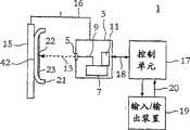
图1以示意性的方式显示了用于生产根据本发明的天线装置的系统。FIG. 1 shows in a schematic way a system for producing an antenna arrangement according to the invention.
图2a-b分别以示意图和透视图的方式显示了用于喷射液态导电物质的装置的第一具体实施例,其包括在如图1所示的用于生产天线装置的代表性系统中。Figures 2a-b show a schematic and a perspective view respectively of a first specific embodiment of a device for ejecting a liquid conductive substance included in a representative system for producing an antenna device as shown in Figure 1 .
图2c以分解透视图的方式显示了用于喷射液态导电物质的印刷头的第二具体实施例,其包括在如图1所示的用于生产天线装置的代表性系统中。Fig. 2c shows, in an exploded perspective view, a second specific embodiment of a printing head for ejecting a liquid conductive substance, which is included in the representative system for producing an antenna device as shown in Fig. 1 .
图2d示意性地显示了如图1所示的用于生产天线装置的系统的一个具体实施例。Fig. 2d schematically shows a specific embodiment of the system for producing an antenna device as shown in Fig. 1 .
图3a-b以顶视图的方式示意性地显示了根据本发明的生产方法所生产出的两个不同的天线图案。Figures 3a-b schematically show in top view two different antenna patterns produced according to the production method of the present invention.
图3c-d以剖视图的方式示意性地显示了根据本发明的生产方法所生产出的另外两个不同的天线图案。3c-d schematically show two other different antenna patterns produced according to the production method of the present invention in cross-sectional view.
图4是根据本发明的另一实施例的方法的流程图。Fig. 4 is a flowchart of a method according to another embodiment of the present invention.
优选实施例的详细介绍Detailed introduction of the preferred embodiment
现在详细地参考附图,在各幅图中相同的标号表示相同或相似的元件,图1是用于生产根据本发明的在便携式无线电通信装置中使用的天线装置的通用系统1的示意图。Referring now in detail to the drawings, in which like numerals indicate like or similar elements throughout the several figures, FIG. 1 is a schematic diagram of a
系统1包括具有喷射开口5的喷射装置3,其通常包括:装有液态导电物质的容器7;将容器7和开口5互连的液体通信路径9;以及用于使液态导电物质最好是作为紧密聚集的液流13或连续的液滴而从容器7中经通信路径和开口5流出的器具11。The
系统1还包括形式为支座、工作台或类似装置的载体15以及装置16如框架或支撑,其用于将喷射装置3和载体15以准确和精密地控制的方式互连,并且使载体15和喷射装置3的喷射开口5在与液流13从开口5中喷射出的方向基本上正交的平面内相互间运动。The
另外,系统1包括通过双向通信线路18与喷射装置3和支撑16相连的控制单元17;以及通过另一双向通信线路20与控制单元17相连的输入/输出(i/o)装置19。控制单元17通常是装有适当软件的微型计算机或类似装置,可控制液态导电物质从开口5中的喷射以及载体15和开口5之间的相对运动。通过形式通常为显示装置和键盘等的输入/输出装置19,操作人员就可控制、改变、改进、调节和监控控制单元17的操作。In addition, the
在用于生产天线装置的系统1的操作中,提供了带有天线图案的适当介质基体。在一种方式中,介质是具有第一表面22和相对的第二表面42的模制塑料21的一部分,其中天线图案形成在其第一表面上,其第二表面构成了天线装置将要安装于其上的便携式无线电通信装置的外壳。然而在此方面并无限制,介质基体实际上可以是仅用于此目的或广泛用于其它目的的任何类型的介质材料。这种介质基体的例子有SIM卡、印制电路板(PCB)、显示屏、键盘、电池和电池组。In operation of the
介质基体21牢固地连接在载体15上,其第二表面朝向载体,而其第一表面朝向喷射装置3。The
然后,载体15和喷射装置的喷射开口5相互间相对运动,同时将液态导电物质喷射到介质基体21的第一表面22上,从而在液态导电物质固化后形成了导电天线图案,其在图1中由标号23表示。Then, the
通过这种设置,就可实现低成本的天线装置的大批量制造。另外,可在各装置中采用很少的部件就可制出非常简单的天线装置。由于印在介质上的天线图案由控制单元和操作人员来控制,因此可以容易地改变、调节和改进图案,无须采用新的物理原型、模板、样板等来进行制造,而这是采用其它一些印刷技术如丝网印刷和刷镀印刷技术所必须的。With this arrangement, low-cost mass production of the antenna device can be realized. In addition, very simple antenna devices can be produced using very few components in each device. Since the antenna pattern printed on the media is controlled by the control unit and the operator, the pattern can be easily changed, adjusted and improved without the need for new physical prototypes, templates, templates, etc. Techniques such as screen printing and brush plating are necessary.
可通过加热喷射到介质基体上的液态导电物质、或者通过在介质基体和喷射于其上的液态导电物质上吹入气体尤其是干燥空气来加速天线图案的固化。Curing of the antenna pattern can be accelerated by heating the liquid conductive substance sprayed onto the dielectric substrate, or by blowing gas, especially dry air, over the dielectric substrate and the liquid conductive substance sprayed thereon.
另外,还可以采用本发明的生产方法来在介质21的第二表面42上形成天线图案。这种双重天线图案可生产用于提高天线装置的射频性能,以允许多频带操作和/或直接在介质基体21上形成电路,例如包括电容器的匹配电路。In addition, the production method of the present invention can also be used to form antenna patterns on the
因此,可从载体15上取出天线装置,将其倒置并重新安装在载体15上,之后将液态导电物质从喷射装置3中喷射到介质基体21的第二表面42上,同时使所述介质基体和所述喷射装置的喷射开口相互间相对运动。在固化之后,在介质基体的第二表面上就形成了第二导电天线图案(未示出)。Therefore, the antenna device can be taken out from the
液态导电物质可以是任何适当的导电流体,例如导电漆、导电树脂或导电粘合剂,喷射装置3可以是任何适于此目的的装置,例如滴射枪(drops gun)、喷雾器、风枪(blow-by gun)和喷漆枪中的一种。The liquid conductive substance can be any suitable conductive fluid, such as conductive paint, conductive resin or conductive adhesive, and the
然而,在本发明的一个优选方式中,液态导电物质为导电墨水,而喷射装置为喷墨印刷机。However, in a preferred mode of the present invention, the liquid conductive substance is conductive ink, and the spraying device is an inkjet printer.
在下文中将介绍适用于本发明的生产工艺的喷墨印刷装置的两个实施例。In the following, two embodiments of an inkjet printing device suitable for the production process of the present invention will be described.
首先参考图2a和2b,图中显示了用于安全、快速和可靠地喷射导电墨水的墨滴的喷墨印刷装置的基本结构,其中墨滴的形成通过热能来实现。墨水由保持在预定高压P3下的墨水供应槽38经导管37提供给印刷通道35。作为高压墨槽的另一选择,印刷通道35可以是毛细通道,能类似地保证墨水从供应槽到印刷开口39的可靠馈送。印刷通道35由基板34和盖板36形成,盖板36设有适当的沟槽。Referring first to Figures 2a and 2b, there is shown the basic structure of an inkjet printing device for safely, rapidly and reliably ejecting ink droplets of conductive ink, wherein the formation of ink droplets is achieved by thermal energy. Ink is supplied to the
喷墨印刷装置通过框架16与固定座15相连以形成一个装置,其中喷墨印刷装置和固定座15以受控方式相互间相对运动。在固定座15内安装了介质基体,其第一表面22朝向印刷开口39。The inkjet printing device is connected to the
墨滴25通过如电阻器33的电热转换器而从印刷开口39喷射到介质基体21的表面22上,介质基体21牢固地安装在固定座15上。在一个优选方式中,电阻器33包括基板34上的薄膜金属层。当在电阻器33上施加适当的电压脉冲时,电阻器附近区域内的墨水温度超过了其熔点,并且形成了墨水气泡。这种爆发性扩展的气泡用于将墨滴5喷射到印刷开口39之外。
如果需要的话,电阻器33上可覆盖传热箔片(未示出),箔片与电阻器紧密接触,并防止电阻器过热烧坏而影响墨水。而且,这种箔片使得电阻器对所用墨水的化学特性不敏感。If necessary, the
当采用高压供墨系统时,如图2a所示的漏油排放系统是有用的。任何离开印刷开口39的过量墨水被低压P4抽吸到进入口40中。设置了侧盖41以形成进入口40。进入口的典型尺寸为约10到500□m(对印刷开口的直径为20到1000□m而言)。An oil spill drain system as shown in Figure 2a is useful when a high pressure ink supply system is used. Any excess ink leaving the
图2c显示了根据另一实施例的喷墨印刷机的单列矩阵印刷头,印刷头具有n个印刷开口。基板44携带有n个电阻器45-1到45-n,其电阻均为约150欧。各电阻器在一端与共用接地电极55相连,电阻器的另一端与电极56-1到56-n相连。基板44与盖板48粘合在一起,盖板48上设有沟槽,其与基板44一起形成了宽度为40□m的印刷通道46-1到46-n,它们全部终止于共用墨槽47处。墨槽47被板51覆盖,板51上设有通气管50以及与供墨槽(未示出)相连的供墨管49-1,49-2。Fig. 2c shows a single column matrix print head of an inkjet printer according to another embodiment, the print head having n printing openings. The substrate 44 carries n resistors 45-1 to 45-n, each of which has a resistance of about 150 ohms. Each resistor is connected at one end to the common ground electrode 55, and the other end of the resistor is connected to the electrodes 56-1 to 56-n. The base plate 44 is glued together with the cover plate 48, which is provided with grooves, which together with the base plate 44 form printing channels 46-1 to 46-n with a width of 40 m, all of which terminate in a common ink tank 47 places. The ink tank 47 is covered by a plate 51 provided with a vent tube 50 and ink supply tubes 49-1, 49-2 connected to ink supply tanks (not shown).
印刷头设有排放系统,其包括具有宽度为30□m的槽53的进入板52,槽53与排放腔54相连,在使用中排放腔54保持在低压下。The print head is provided with a discharge system comprising an inlet plate 52 with a slot 53 of width 30 m connected to a discharge chamber 54 which is kept under low pressure in use.
在操作中,在共用接地电极55和一个或多个电极56-1到56-n之间施加电压脉冲,这样在印刷头和记录媒体相互间相对运动时就可进行矩阵式印刷。In operation, voltage pulses are applied between the common ground electrode 55 and one or more of the electrodes 56-1 through 56-n such that matrix printing occurs as the printhead and recording medium move relative to each other.
在上文中通过参考各印刷开口由各个印刷通道的端部形成的装置来介绍了上述实施例。然而,它对印刷开口沿一个或多个印刷通道的长度设置的装置同样适用,在这种情况下墨滴侧向地从通道中喷射出。The above embodiments have been described above with reference to an arrangement in which each printing opening is formed by the end of each printing channel. However, it is equally applicable to arrangements in which the printing openings are arranged along the length of one or more printing channels, in which case ink drops are ejected laterally from the channels.
虽然通过示例在两个实施例中介绍了用于本发明的喷墨印刷装置,然而应当理解,本发明可以多种方式进行变化。这种关于喷墨印刷机和喷墨印刷技术的其它变化可见于授予Hertz等人的美国专利No.4050075和授予Belon等人的美国专利No.6155680,这些专利在此用作参考,并通过引用结合于本文中。Although the inkjet printing apparatus used in the present invention has been described in two embodiments by way of example, it should be understood that the invention can be varied in many ways. Such other variations on inkjet printers and inkjet printing technology can be found in U.S. Patent No. 4,050,075 to Hertz et al. and U.S. Patent No. 6,155,680 to Belon et al., which are hereby incorporated by reference and incorporated herein by reference incorporated in this article.
下面将参考图2d来介绍本发明的一个重要特征,图2d示意性地显示了用于生产图1所示天线装置的系统的一个具体实施例。An important feature of the present invention will now be described with reference to FIG. 2d, which schematically shows a specific embodiment of the system for producing the antenna device shown in FIG. 1 .
系统包括具有容器7、导管9和印刷头60的印刷机装置,印刷头具有开口,导电漆或墨水可从此开口中沿箭头61所示的方向喷射出。系统还包括可在箭头65所示的三维方向上运动的工作台63。工作台例如可以是在与墨水或漆从印刷头60中喷射出的方向61正交的XY平面内运动的XY工作台,其还可设有用于使工作台在与XY平面正交的第三方向Z上运动的装置。The system comprises a printer unit with a
工作台63的运动以及墨水或漆从印刷机装置中的喷射由控制单元17分别通过控制线路18和62来控制。在图1所示的系统中,控制单元设有经通信线路20相连的输入/输出装置18。The movement of the table 63 and the ejection of ink or varnish from the printing press arrangement is controlled by the
通过图2d所示的系统,就可以在基本上为非平面的表面如弯曲、凸出和下凹表面上形成天线图案,并且在印刷头的开口和待形成天线图案的非平面表面之间保持基本上恒定的距离。With the system shown in Figure 2d, it is possible to form antenna patterns on substantially non-planar surfaces such as curved, convex and concave surfaces, and maintain substantially constant distance.
在操作中,将具有将在其上形成天线图案的基本上为非平面的表面的介质基体21安装在工作台63上,之后工作台63在XY平面上和在Z方向上运动,同时从印刷头60中喷出液态导电物质。XY方向上的运动代表待生产的天线图案,Z方向上的运动用于随从介质基体21的非平面表面,即在生产期间实现离介质基体21的非平面表面为恒定的距离。因此,Z方向上的运动用于将印刷头60的开口保持在虚线66所示的水平上。In operation, the
下面将参考图3a和3b来介绍根据本发明的生产方法所生产出的两个不同的天线装置,图3a和3b示意性地显示了顶视图。Two different antenna arrangements produced according to the production method of the invention will be described below with reference to Figures 3a and 3b, which schematically show top views.
图3a显示了包括有生产于介质基体21、例如刚性或柔性基体上的弯曲图案71的天线装置。采用柔性基体可使基体的形状适于其将安装到的便携式无线电通信装置的外壳形状。Figure 3a shows an antenna arrangement comprising a curved pattern 71 produced on a
弯曲形天线图案71具有馈送连接点72以及多个平行的馈线和接地线73,它们分别通过共用主馈线75和接地线76与馈电点72和接地点74相连。天线器件还包括另外的电容元件77以及接地的电感元件78。虚线79表示了可调节天线图案1的长度的一些位置。标号80表示天线器件的不同点之间的短路线。The meander antenna pattern 71 has a feeding connection point 72 and a plurality of parallel feeding and grounding lines 73, which are respectively connected to the feeding point 72 and the grounding point 74 through a common main feeding line 75 and a grounding line 76. The antenna device also comprises a further capacitive element 77 and an inductive element 78 connected to ground. Dotted lines 79 indicate some positions where the length of the
电容和电感元件77,78显示为分立元件。然而,如本领域中已知的那样,通过与天线器件的导电路径相同类型的并与天线器件施加在同一基体上且相连的适当形成的导电路径,可以容易地提供所需的电容或电感。Capacitive and inductive elements 77, 78 are shown as discrete components. However, the required capacitance or inductance can readily be provided by suitably formed conductive paths of the same type as those of the antenna device and applied to and connected to the same substrate as the antenna device, as is known in the art.
图3b显示了根据本发明的形成于基体21上的另一弯曲形天线图案82。天线图案82在点83处接地。主馈线84使共用馈送接头85与多个馈送分支86相连。一些馈送分支86包括适当的电容和/或电感87。在天线图案上增设了一些调谐短截线88,这些短截线根据需要而形成,用于带频的精确频率调谐。Fig. 3b shows another
现在来看示意性地显示了剖视图的图3c和3d,将介绍根据本发明的生产方法所生产出的另外两个天线图案。Referring now to Figures 3c and 3d, which schematically show cross-sectional views, two further antenna patterns produced according to the production method of the invention will be presented.
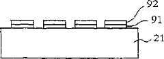
根据第一生产工艺,通过如图1-2所示的任一装置在介质基体上形成液态物质的图案91,其结果显示于图3c中。液态物质可以是导电墨水,其通过揉合导电颜料和粘合剂与溶剂的混合物来得到。所用的粘合剂可从甲基丙烯酸酯树脂如ABS树脂、乙基纤维素和苯酚树脂中选择。所用的溶剂可从丙酮、乙酸乙酯、溶纤剂衍生物、甲酮、苯、甲苯和氯乙烯中选择。所用的导电颜料可从银粉末、氧化银、硝酸银、银的有机化合物和铜粉末中选择。According to the first production process, a
导电墨水层91设置成使得金属镀层92能令人满意地粘附在其上。可在导电墨水层91上选择性地化学电镀导电金属如镍或铜的金属层92,使得金属镀层92得到与图案91基本上匹配并覆盖于其上的图案。
作为选择,可以从导电墨水层91中蚀刻去导电墨水中的粘合剂,使得其表面变粗糙,然后在存在有催化剂如铂的情况下在墨水层92的粗糙表面上化学电镀导电金属如镍或铜。Alternatively, the binder in the conductive ink can be etched away from the
这样形成的导电墨水层91和金属镀层92提高了天线装置的天线性能。The
金属也可采用离子电镀或电解电镀来代替化学电镀。Metals can also be plated by ion plating or electrolytic plating instead of chemical plating.
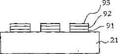
现在参考图3d,通过采用本发明的上述实施例和方式的喷射或印刷装置中的任一种来形成导电墨水图案91,通过选择性化学电镀在导电墨水层91上形成金属图案92,并在化学电镀的图案92上选择性地形成电解电镀的金属层93,从而生产出天线装置。With reference to Fig. 3 d now, form
化学镀层92通过将导电金属选择性地化学电镀到导电墨水层91上来形成,电解电镀层93通过在化学镀层24上进行选择性的电解电镀来形成,使得三种图案相互对应和对齐以便相互重叠。The
与化学电镀相比,电解电镀可实现厚度更大的电镀图案,因此图3d所示的天线装置比图3c所示的天线装置具有更大量的导电金属。Compared with electroless plating, electrolytic plating can achieve a thicker plating pattern, so the antenna device shown in Fig. 3d has a larger amount of conductive metal than the antenna device shown in Fig. 3c.
应当理解,虽然重叠在印在介质基体上的原始图案上的镀金属自身可作为天线来操作,然而主要形成于介质基体上的液态物质可以是电绝缘材料。It should be understood that while the metallization superimposed on the original pattern printed on the dielectric substrate may itself operate as an antenna, the liquid substance formed primarily on the dielectric substrate may be an electrically insulating material.
关于选择性金属电镀的更多细节可见于授予Sonoda等人的美国专利No.5768217和授予Dupuis等人的美国专利No.5685898,这些专利通过引用结合于本文中。More details on selective metal plating can be found in US Patent No. 5,768,217 to Sonoda et al. and US Patent No. 5,685,898 to Dupuis et al., which are incorporated herein by reference.
现在将参考图4来介绍本发明的另一实施例,图4是可重复进行的生产工艺的流程图。Another embodiment of the present invention will now be described with reference to FIG. 4, which is a flow chart of a repeatable manufacturing process.
由于根据例如参考图1所介绍的方法的天线装置的生产比较灵活,因此它可与包括有决策模型的可重复的生产工艺有利地结合,其中可在生产线上调节、校正或更改天线装置。Since the production of the antenna arrangement according to the method described with reference to FIG. 1 is relatively flexible, it can advantageously be combined with a repeatable production process including a decision model in which the antenna arrangement can be adjusted, corrected or changed on the production line.
在工艺的第一工序101中,根据参考图1所介绍的方法来在介质基体上形成天线图案。之后在工序103中,将其上形成有天线图案的介质基体和特定形式的便携式无线电通信装置装配起来,其中天线图案与所述特定形式的便携式无线电通信装置的射频馈送装置电连接。之后在工序105中,在装配好的特定形式的便携式无线电通信装置的操作期间测量/检测至少一项天线特性。所测量的天线特性例如为天线增益、回波损耗、远场、近场或SAR特性。In the first step 101 of the process, an antenna pattern is formed on a dielectric substrate according to the method described with reference to FIG. 1 . Then in step 103, the dielectric substrate on which the antenna pattern is formed is assembled with a specific type of portable radio communication device, wherein the antenna pattern is electrically connected to the radio frequency feeding device of the specific type of portable radio communication device. Thereafter in process step 105 at least one antenna characteristic is measured/detected during operation of the assembled particular form of portable radio communication device. The measured antenna properties are, for example, antenna gain, return loss, far-field, near-field or SAR properties.
在测试后,在工序107中将其上形成有所述天线图案的介质基体和特定形式的便携式无线电通信装置拆开,其中天线图案与便携式无线电通信装置的射频馈送装置电脱离。After the test, the dielectric substrate on which the antenna pattern is formed and the specific type of portable radio communication device are disassembled in process 107, wherein the antenna pattern is electrically detached from the RF feeding device of the portable radio communication device.
所测得的天线特性在工序109中用于决策模型,以确定此特性是可以接受、并不能完全接受但在对天线图案进行一定改进后可以接受,还是完全不能接受。最后在工序111中根据所采用的决定来对带有天线图案的介质进行分类:如果特性可接受,此带有天线图案的介质就被批准为所生产出的天线装置;如果完全不能接受,那么此带有天线图案的介质就被拒绝;如果带有天线图案的介质需要改进,那么它在工序113中返回到喷射装置,使得在工序101中再次在介质上形成另一改进过的导电天线图案。然后此工艺继续进行工序103-111,直到带有天线图案或改进过的天线图案的介质最终被批准或拒绝。The measured antenna characteristics are used in a decision model in step 109 to determine whether the characteristics are acceptable, not completely acceptable but acceptable with certain improvements to the antenna pattern, or not acceptable at all. Finally, in operation 111, the medium with the antenna pattern is classified according to the adopted decision: if the characteristics are acceptable, the medium with the antenna pattern is approved as the produced antenna device; if it is not acceptable at all, then This medium with the antenna pattern is just rejected; if the medium with the antenna pattern needs to be improved, it is returned to the jetting device in operation 113 so that another improved conductive antenna pattern is formed on the medium again in operation 101 . The process then continues with steps 103-111 until the medium with the antenna pattern or modified antenna pattern is finally approved or rejected.
另外,此生产工艺可设置成,根据所测得的天线特性,形成于介质基体上的一部分天线图案尤其可通过激光切割来去除。Furthermore, the production process can be configured such that, depending on the measured antenna properties, a part of the antenna pattern formed on the dielectric substrate can be removed, in particular by laser cutting.
回到图3a和3b,天线图案的一些细节可以是上述改进和调节的结果。例如,图3a中所示的天线图案的元件73,77,78和在79和80处的图案长度以及图3b中所示的天线图案的元件87和88都是可应用到初始形成的天线图案上的附加结构的例子。类似地,图3a和3b所示的天线图案中的虚线圆81表示了通过去除天线材料而断开电通路的位置。Returning to Figures 3a and 3b, some details of the antenna pattern may be the result of the improvements and adjustments described above. For example, elements 73, 77, 78 of the antenna pattern shown in FIG. 3a and the pattern lengths at 79 and 80 and
应当理解,上述生产工艺介绍可应用于特定天线装置的大批量生产的初始阶段中。因此,具有改进天线图案的最终批准的天线装置可用作模板,以便用于特定形式的便携式无线电通信装置的天线装置的大批量生产。It should be understood that the above description of the production process is applicable in the initial stages of mass production of a particular antenna arrangement. Thus, the final approved antenna arrangement with the improved antenna pattern can be used as a template for mass production of the antenna arrangement for a particular form of portable radio communication device.
在本发明人的于1999年12月23日提交的题为“用于制造天线装置的方法和坯件”的未决瑞典专利申请No.9904773-0以及于2000年11月22日提交的题为“生产测量装置”的瑞典专利申请No.0004280-4中进一步介绍了关于改进、再设计和生产测量的方面,这些专利申请通过引用结合于本文中。In the inventor's pending Swedish patent application No. 9904773-0, filed on 23.12.1999, entitled "Method and blank for manufacturing an antenna arrangement" and filed on 22.11.2000 Aspects of improvement, redesign and production measurement are further described in Swedish Patent Application No. 0004280-4 entitled "Production Measurement Device", which patent application is hereby incorporated by reference.
Claims (27)
Translated fromChineseApplications Claiming Priority (2)
| Application Number | Priority Date | Filing Date | Title |
|---|---|---|---|
| SE0004909ASE519904C2 (en) | 2000-12-29 | 2000-12-29 | Manufacture of antenna devices |
| SE00049098 | 2000-12-29 |
Publications (2)
| Publication Number | Publication Date |
|---|---|
| CN1484935A CN1484935A (en) | 2004-03-24 |
| CN1235455Ctrue CN1235455C (en) | 2006-01-04 |
Family
ID=20282484
Family Applications (1)
| Application Number | Title | Priority Date | Filing Date |
|---|---|---|---|
| CNB018216595AExpired - Fee RelatedCN1235455C (en) | 2000-12-29 | 2001-12-21 | Method for producing an antenna device for a portable radio communication device |
Country Status (6)
| Country | Link |
|---|---|
| US (1) | US7480979B2 (en) |
| EP (1) | EP1346616A1 (en) |
| KR (1) | KR100562769B1 (en) |
| CN (1) | CN1235455C (en) |
| SE (1) | SE519904C2 (en) |
| WO (1) | WO2002054841A1 (en) |
Families Citing this family (22)
| Publication number | Priority date | Publication date | Assignee | Title |
|---|---|---|---|---|
| JP4251041B2 (en)* | 2002-08-30 | 2009-04-08 | セイコーエプソン株式会社 | Liquid ejector |
| JP2006156943A (en)* | 2004-09-28 | 2006-06-15 | Seiko Epson Corp | Wiring pattern forming method, wiring pattern, and electronic device |
| US7354794B2 (en) | 2005-02-18 | 2008-04-08 | Lexmark International, Inc. | Printed conductive connectors |
| CA2516141A1 (en)* | 2005-08-17 | 2007-02-17 | Intelligent Devices Inc. | Printing press control system |
| EP1855514A1 (en)* | 2006-05-10 | 2007-11-14 | AMC Centurion AB | Production of antenna devices |
| EP1914832A1 (en)* | 2006-10-17 | 2008-04-23 | Laird Technologies AB | A method of production of an antenna pattern |
| KR100845117B1 (en)* | 2007-02-21 | 2008-07-10 | 김효순 | Antenna and its manufacturing method |
| GB2453765A (en)* | 2007-10-18 | 2009-04-22 | Novalia Ltd | Product packaging with printed circuit and means for preventing a short circuit |
| KR100857615B1 (en)* | 2008-01-22 | 2008-09-09 | (주)휴먼테크 | Method of manufacturing RDF antenna |
| US7898484B1 (en) | 2008-05-12 | 2011-03-01 | The United States Of America As Represented By The Secretary Of The Navy | Electrolytic fluid antenna |
| EP2291884A4 (en)* | 2008-05-19 | 2013-01-02 | Galtronics Corp Ltd | Conformable antenna |
| CN102148422A (en)* | 2011-02-23 | 2011-08-10 | 中兴通讯股份有限公司 | Frequency-modulated antenna realization device and mobile terminal |
| TWI482361B (en) | 2012-01-18 | 2015-04-21 | Cirocomm Technology Corp | Automatic testing and trimming method for planar antenna and system for the same |
| DE112013001263T5 (en)* | 2012-03-02 | 2015-04-30 | Pulse Electronics, Inc. | Remote antenna device and method therefor |
| CN104178721B (en)* | 2013-05-22 | 2016-08-10 | 中国科学院理化技术研究所 | Device and method for directly manufacturing conductive film at room temperature |
| US10020561B2 (en) | 2013-09-19 | 2018-07-10 | Pulse Finland Oy | Deposited three-dimensional antenna apparatus and methods |
| CN106463828B (en)* | 2014-02-12 | 2021-04-06 | 脉冲芬兰有限公司 | Method and apparatus for conductive element deposition and formation |
| US9833802B2 (en) | 2014-06-27 | 2017-12-05 | Pulse Finland Oy | Methods and apparatus for conductive element deposition and formation |
| DE202014103821U1 (en)* | 2014-07-09 | 2014-09-09 | Carmen Diegel | Flexible electrical conductor structure |
| CN104966684A (en)* | 2015-06-10 | 2015-10-07 | 江苏杰进微电子科技有限公司 | Integrated circuit chip binding equipment and working method thereof |
| US10164328B2 (en) | 2016-09-08 | 2018-12-25 | The United States Of America As Represented By Secretary Of The Navy | Method and apparatus for optical agitation of electrolytes in a fluid-based antenna |
| CN110137687A (en)* | 2019-05-29 | 2019-08-16 | 兰州大学 | A method of preparing flexible Meta Materials |
Family Cites Families (15)
| Publication number | Priority date | Publication date | Assignee | Title |
|---|---|---|---|---|
| DK648187D0 (en)* | 1987-12-09 | 1987-12-09 | Linkease Test Systems A S | METHOD AND APPARATUS FOR CIRCUIT MANUFACTURING |
| SE465713B (en)* | 1990-02-12 | 1991-10-21 | Mydata Automation Ab | DEVICE FOR PREPARING PASTORS AND LIMS |
| US6120588A (en)* | 1996-07-19 | 2000-09-19 | E Ink Corporation | Electronically addressable microencapsulated ink and display thereof |
| JPH09307329A (en)* | 1996-05-14 | 1997-11-28 | Casio Comput Co Ltd | Antenna, manufacturing method thereof, and electronic device or electronic timepiece equipped with the antenna |
| BR9908158A (en)* | 1998-02-23 | 2001-09-04 | Qualcomm Inc | Two-band uniplanar antenna |
| JPH11312881A (en)* | 1998-04-28 | 1999-11-09 | Matsushita Electric Ind Co Ltd | Substrate bonding method, high-frequency circuit, antenna, waveguide, line converter, line branch circuit, and communication system |
| US6175752B1 (en)* | 1998-04-30 | 2001-01-16 | Therasense, Inc. | Analyte monitoring device and methods of use |
| US6697694B2 (en)* | 1998-08-26 | 2004-02-24 | Electronic Materials, L.L.C. | Apparatus and method for creating flexible circuits |
| KR100629923B1 (en) | 1998-09-30 | 2006-09-29 | 돗빤호무즈가부시기가이샤 | Conductive paste, curing method therof, method for fabricating antenna for contactless data transmitter-receiver, and contactless data transmitter-receiver |
| GB2345196B (en)* | 1998-12-23 | 2003-11-26 | Nokia Mobile Phones Ltd | An antenna and method of production |
| FR2795234B1 (en)* | 1999-06-15 | 2003-07-18 | Gemplus Card Int | METHOD FOR MANUFACTURING ALL OR PART OF AN ELECTRONIC DEVICE BY JET OF MATERIAL |
| US6973709B2 (en)* | 2001-04-19 | 2005-12-13 | Chunghwa Picture Tubes | Method of manufacturing printed-on-display antenna for wireless device |
| US7102522B2 (en)* | 2002-12-24 | 2006-09-05 | 3M Innovative Properties Company | Tamper-indicating radio frequency identification antenna and sticker, a radio frequency identification antenna, and methods of using the same |
| US7192107B2 (en)* | 2003-04-21 | 2007-03-20 | Seiko Epson Corporation | Information communicating member, liquid container having information communicating member and liquid ejecting apparatus |
| JP3788467B2 (en)* | 2003-05-28 | 2006-06-21 | セイコーエプソン株式会社 | Pattern forming method, device and device manufacturing method, electro-optical device, electronic apparatus, and active matrix substrate manufacturing method |
- 2000
- 2000-12-29SESE0004909Apatent/SE519904C2/ennot_activeIP Right Cessation
- 2001
- 2001-12-21KRKR1020037008779Apatent/KR100562769B1/ennot_activeExpired - Fee Related
- 2001-12-21CNCNB018216595Apatent/CN1235455C/ennot_activeExpired - Fee Related
- 2001-12-21USUS10/451,437patent/US7480979B2/ennot_activeExpired - Fee Related
- 2001-12-21EPEP01272992Apatent/EP1346616A1/ennot_activeWithdrawn
- 2001-12-21WOPCT/SE2001/002885patent/WO2002054841A1/enactiveIP Right Grant
Also Published As
| Publication number | Publication date |
|---|---|
| KR20030064889A (en) | 2003-08-02 |
| SE519904C2 (en) | 2003-04-22 |
| SE0004909D0 (en) | 2000-12-29 |
| CN1484935A (en) | 2004-03-24 |
| SE0004909L (en) | 2001-11-09 |
| US7480979B2 (en) | 2009-01-27 |
| KR100562769B1 (en) | 2006-03-20 |
| WO2002054841A1 (en) | 2002-07-11 |
| US20040060162A1 (en) | 2004-04-01 |
| EP1346616A1 (en) | 2003-09-24 |
Similar Documents
| Publication | Publication Date | Title |
|---|---|---|
| CN1235455C (en) | Method for producing an antenna device for a portable radio communication device | |
| KR101701620B1 (en) | Methods and apparatus for conductive element deposition and formation | |
| US9780438B2 (en) | Deposition antenna apparatus and methods | |
| CN1085967C (en) | Ink jet print head and nozzle plate used therefor | |
| US8585187B2 (en) | High density electrical interconnect for printing devices using flex circuits and dielectric underfill | |
| CN1870860A (en) | Electronic substrate manufacturing method, semiconductor device, and manufacturing method of electronic machine | |
| EP1855514A1 (en) | Production of antenna devices | |
| TW201351772A (en) | Methods for forming elongated antennas with plastic support structures for electronic devices | |
| KR100662837B1 (en) | Method for forming multi-layered structure, method for manufacturing wiring substrate, and method for manufacturing electronic apparatus | |
| TW201545407A (en) | Methods and apparatus for conductive element deposition and formation | |
| CN1776904A (en) | Installation of substrates and electronic devices | |
| Salonen et al. | Direct printing of a handset antenna on a 3D surface | |
| TWI277459B (en) | Wiring board, manufacturing method thereof, and electronic appliance | |
| CN1838351A (en) | Multi-layer ceramic electronic component and production method thereof | |
| JP2009255447A (en) | Inkjet recording head | |
| CN1717154A (en) | shielded wire | |
| CN211789499U (en) | Antenna for improving low-frequency bandwidth | |
| CN115348743B (en) | Method for printing circuit on curved carrier and curved printed circuit | |
| CN113394551B (en) | Antenna for improving low-frequency bandwidth | |
| Chew et al. | Electroless Plating with Copper Complex Ink as a Seed | |
| WO2025149986A1 (en) | High-performance, low signal loss, high-density, multi-layer, double-sided 3d printed circuit structure deposition and fabrication platform | |
| HK1204156B (en) | Deposition antenna apparatus and methods | |
| CN1640671A (en) | Inkjet print head and manufacturing method thereof | |
| JPH032195B2 (en) | ||
| JP2008124294A (en) | Electronic substrate and manufacturing method thereof |
Legal Events
| Date | Code | Title | Description |
|---|---|---|---|
| C06 | Publication | ||
| PB01 | Publication | ||
| C10 | Entry into substantive examination | ||
| SE01 | Entry into force of request for substantive examination | ||
| C14 | Grant of patent or utility model | ||
| GR01 | Patent grant | ||
| C41 | Transfer of patent application or patent right or utility model | ||
| TR01 | Transfer of patent right | Effective date of registration:20090123 Address after:Heping District, Shenzhen, Baoan District, Fuyong, Guangdong Province, Heping community, Luther King Industrial Park, a district Patentee after:Laird Technologies Inc. Address before:Swedish O Kersh Beria Patentee before:AMC Centenary AB | |
| ASS | Succession or assignment of patent right | Owner name:LAIRD ELECTRON MATERIAL ( SHENZHEN ) CO., LTD. Free format text:FORMER OWNER: AMC SHIJI CO., LTD. Effective date:20090123 | |
| TR01 | Transfer of patent right | ||
| TR01 | Transfer of patent right | Effective date of registration:20200727 Address after:201900 room w-2546, no.559 yueluo Road, Baoshan District, Shanghai Patentee after:Kedi (Shanghai) Trading Co.,Ltd. Address before:518103 Luther King Industrial Park, Fu Fu Garden, Heping community, Fuyong Town, Shenzhen, Guangdong, Baoan District Patentee before:Laide electronic materials (Shenzhen) Co.,Ltd. | |
| CF01 | Termination of patent right due to non-payment of annual fee | Granted publication date:20060104 Termination date:20201221 | |
| CF01 | Termination of patent right due to non-payment of annual fee |