CN1233058A - boost circuit - Google Patents
boost circuitDownload PDFInfo
- Publication number
- CN1233058A CN1233058ACN99105833ACN99105833ACN1233058ACN 1233058 ACN1233058 ACN 1233058ACN 99105833 ACN99105833 ACN 99105833ACN 99105833 ACN99105833 ACN 99105833ACN 1233058 ACN1233058 ACN 1233058A
- Authority
- CN
- China
- Prior art keywords
- field effect
- effect transistor
- boost
- circuit
- boosting
- Prior art date
- Legal status (The legal status is an assumption and is not a legal conclusion. Google has not performed a legal analysis and makes no representation as to the accuracy of the status listed.)
- Pending
Links
Images


Classifications
- H—ELECTRICITY
- H02—GENERATION; CONVERSION OR DISTRIBUTION OF ELECTRIC POWER
- H02M—APPARATUS FOR CONVERSION BETWEEN AC AND AC, BETWEEN AC AND DC, OR BETWEEN DC AND DC, AND FOR USE WITH MAINS OR SIMILAR POWER SUPPLY SYSTEMS; CONVERSION OF DC OR AC INPUT POWER INTO SURGE OUTPUT POWER; CONTROL OR REGULATION THEREOF
- H02M3/00—Conversion of DC power input into DC power output
- H02M3/02—Conversion of DC power input into DC power output without intermediate conversion into AC
- H02M3/04—Conversion of DC power input into DC power output without intermediate conversion into AC by static converters
- H02M3/06—Conversion of DC power input into DC power output without intermediate conversion into AC by static converters using resistors or capacitors, e.g. potential divider
- H02M3/07—Conversion of DC power input into DC power output without intermediate conversion into AC by static converters using resistors or capacitors, e.g. potential divider using capacitors charged and discharged alternately by semiconductor devices with control electrode, e.g. charge pumps
- H02M3/073—Charge pumps of the Schenkel-type
- G—PHYSICS
- G11—INFORMATION STORAGE
- G11C—STATIC STORES
- G11C11/00—Digital stores characterised by the use of particular electric or magnetic storage elements; Storage elements therefor
- G11C11/21—Digital stores characterised by the use of particular electric or magnetic storage elements; Storage elements therefor using electric elements
- G11C11/34—Digital stores characterised by the use of particular electric or magnetic storage elements; Storage elements therefor using electric elements using semiconductor devices
- G11C11/40—Digital stores characterised by the use of particular electric or magnetic storage elements; Storage elements therefor using electric elements using semiconductor devices using transistors
- G11C11/401—Digital stores characterised by the use of particular electric or magnetic storage elements; Storage elements therefor using electric elements using semiconductor devices using transistors forming cells needing refreshing or charge regeneration, i.e. dynamic cells
- G11C11/403—Digital stores characterised by the use of particular electric or magnetic storage elements; Storage elements therefor using electric elements using semiconductor devices using transistors forming cells needing refreshing or charge regeneration, i.e. dynamic cells with charge regeneration common to a multiplicity of memory cells, i.e. external refresh
- G11C11/404—Digital stores characterised by the use of particular electric or magnetic storage elements; Storage elements therefor using electric elements using semiconductor devices using transistors forming cells needing refreshing or charge regeneration, i.e. dynamic cells with charge regeneration common to a multiplicity of memory cells, i.e. external refresh with one charge-transfer gate, e.g. MOS transistor, per cell
- H—ELECTRICITY
- H02—GENERATION; CONVERSION OR DISTRIBUTION OF ELECTRIC POWER
- H02M—APPARATUS FOR CONVERSION BETWEEN AC AND AC, BETWEEN AC AND DC, OR BETWEEN DC AND DC, AND FOR USE WITH MAINS OR SIMILAR POWER SUPPLY SYSTEMS; CONVERSION OF DC OR AC INPUT POWER INTO SURGE OUTPUT POWER; CONTROL OR REGULATION THEREOF
- H02M1/00—Details of apparatus for conversion
- H02M1/0003—Details of control, feedback or regulation circuits
- H02M1/0032—Control circuits allowing low power mode operation, e.g. in standby mode
- Y—GENERAL TAGGING OF NEW TECHNOLOGICAL DEVELOPMENTS; GENERAL TAGGING OF CROSS-SECTIONAL TECHNOLOGIES SPANNING OVER SEVERAL SECTIONS OF THE IPC; TECHNICAL SUBJECTS COVERED BY FORMER USPC CROSS-REFERENCE ART COLLECTIONS [XRACs] AND DIGESTS
- Y02—TECHNOLOGIES OR APPLICATIONS FOR MITIGATION OR ADAPTATION AGAINST CLIMATE CHANGE
- Y02B—CLIMATE CHANGE MITIGATION TECHNOLOGIES RELATED TO BUILDINGS, e.g. HOUSING, HOUSE APPLIANCES OR RELATED END-USER APPLICATIONS
- Y02B70/00—Technologies for an efficient end-user side electric power management and consumption
- Y02B70/10—Technologies improving the efficiency by using switched-mode power supplies [SMPS], i.e. efficient power electronics conversion e.g. power factor correction or reduction of losses in power supplies or efficient standby modes
Landscapes
- Engineering & Computer Science (AREA)
- Microelectronics & Electronic Packaging (AREA)
- Power Engineering (AREA)
- Computer Hardware Design (AREA)
- Dc-Dc Converters (AREA)
- Dram (AREA)
- Amplifiers (AREA)
- Read Only Memory (AREA)
- Semiconductor Integrated Circuits (AREA)
- Static Random-Access Memory (AREA)
Abstract
Translated fromChinese
Description
Translated fromChinese本发明涉及读取数据等操作的升压电路,尤其涉及有将升压值控制在所需范围之内功能的升压电路。The present invention relates to a voltage boosting circuit for reading data, and in particular to a voltage boosting circuit with the function of controlling the voltage boost value within a required range.
通常,当读取半导体存储器中存放的数据时,升压电路用于给字线升压。例如第6-60651号日本专利申请未决公开中所述的常规升压电路。图1是说明第6-60651号日本专利申请未决公开中所述常规升压电路的电路图。Generally, a boost circuit is used to boost voltage of a word line when reading data stored in a semiconductor memory. For example, a conventional booster circuit described in Japanese Patent Application Laid-Open No. 6-60651. FIG. 1 is a circuit diagram illustrating a conventional boosting circuit described in Japanese Patent Application Laid-Open Publication No. 6-60651.
在常规升压电路中,升压启动信号ATDBST输入到反相器505的输入端,从升压节点NDBST输出电压Vboost。反相器505的输出端接到反相器506的输入端、N-沟道MOS晶体管503的栅极和P-沟道MOS晶体管501的栅极。反相器506的输出端接到电容值为Cb的升压电容507的一端,升压电容507的另一端接到升压节点NDBST。In a conventional boost circuit, the boost start signal ATDBST is input to the input terminal of the
N-沟道MOS晶体管503的漏极接地,它的源极接到N-沟道MOS晶体管504的漏极,N-沟道MOS晶体管504的源极接到P-沟道MOS晶体管502的栅极,把连接点VX与P-沟道MOS晶体管501的一个输入/输出端连接。The drain of N-
电源电压VCC一直提供给N-沟道MOS晶体管504的栅极,并且N-沟道MOS晶体管一直为导通状态。进一步说,P-沟道MOS晶体管502的一个输入端接电源电压VCC,另一个输入/输出端接到升压节点NDBST。P-沟道MOS晶体管501的另一个输入/输出端也接到升压节点NDBST。The power supply voltage VCC is always supplied to the gate of the N-
在有上述结构的常规升压电路中,当处于升压前的等待状态时,升压启动信号ATDBST以低电平输入给反相器505。反相器505将升压启动信号ATDBST的电平反相,VCC电平的信号输入给反相器506的输入端、N-沟道MOS晶体管503的栅极和P沟道MOS晶体管501的栅极。In the conventional boost circuit having the above-mentioned structure, when it is in the standby state before boosting, the boost start signal ATDBST is input to the
按照上述操作,反相器506的输出信号维持低电平,并将低电平信号输入给升压电容器507。According to the above operation, the output signal of the
N-沟道MOS晶体管503进入导通状态,并且升压节点NDBST和P-沟道MOS晶体管502的栅极电平(节点VX)被维持在低电平。因此,假定P-沟道MOS晶体管502为导通状态,此时P-沟道MOS晶体管501处于截止状态。由于P-沟道MOS晶体管502导通,使升压节点NDBST达到电源电压值VCC。The N-
当从此状态开始升压时,升压启动信号ATDBST从低电平转换为高电平VCC,并输入到反相器505的输入端。When boosting is started from this state, the boost start signal ATDBST is switched from a low level to a high level VCC, and is input to the input terminal of the
按照这个操作,反相器505的输出信号从高电平VCC转换为低电平,而反相器506的输出信号从低电平转换为高电平VCC。According to this operation, the output signal of the
因此,VCC高电平信号加到电容器507的一端,低电平信号输入给N-沟道MOS晶体管503的栅极和P-沟道MOS晶体管501的栅极。当VCC高电平信号提供给电容器507的一端时,升压节点NDBST从电源电压VCC电平升压至等式(1)所示的电压值,该值为在电容器507中由电容耦合得到的。Therefore, a VCC high-level signal is applied to one end of the
Vboost=(1+(Cb/(Cb+CL)))×VCC …(1)Vboost=(1+(Cb/(Cb+CL)))×VCC …(1)
当升压完成时,升压启动信号ATDBST的输入电平从高电平转换为低电平,因此各节点的电压值恢复到升压启动前的状态,然后升压完成。When the boost is completed, the input level of the boost start signal ATDBST is switched from high level to low level, so the voltage value of each node returns to the state before the boost start, and then the boost is completed.
当从非易失半导体存储器中读取数据、把所述常规升压电路用作指定字线的升压器时,由于需要确保导通单元和关断单元读取范围,必须把升压电平控制在上限指标和下限指标之间。When reading data from a nonvolatile semiconductor memory and using the conventional boost circuit as a booster for a specified word line, the boost level must be set to It is controlled between the upper limit index and the lower limit index.
然而存在这样一个问题,即最优先控制达到下限指标的同时也要达到上限指标是非常困难的。However, there is such a problem that it is very difficult to achieve the upper limit target while the highest priority control reaches the lower limit target.
原因是该电路的升压值依赖电源电压,如上所述,该升压值和电源电压约为等式(1)所示的两倍关系。The reason is that the boost value of this circuit is dependent on the power supply voltage, and as mentioned above, the boost value and the power supply voltage have approximately twice the relationship shown in equation (1).
进一步说,在从非易失半导体存储器中读取数据时,如果常规升压电路用作为指定字线升压,当字线电压过分增加时,存储单元栅极开始升压,其漏极电平变为1伏左右,从而建立了一个伪弱写方式,因此重复进行读操作,这样就存在一个由伪弱写操作引起存储单元阈值变化的问题。Furthermore, when reading data from a non-volatile semiconductor memory, if a conventional boost circuit is used as a designated word line boost, when the word line voltage increases excessively, the gate of the memory cell starts to boost, and its drain level becomes about 1 volt, thereby establishing a pseudo-weak write mode, so the read operation is repeated, so there is a problem that the threshold value of the memory cell changes due to the pseudo-weak write operation.
原因是该电路的升压值依赖电源电压,该升压值和电源电压约为两倍的关系。The reason is that the boost value of this circuit depends on the power supply voltage, and the relationship between the boost value and the power supply voltage is about twice.
本发明的一个目的是提供一种升压电路,即使当被升压的电位比电源电压高许多时,其也能够稳定控制升压电位,使升压指标上限不取决于电源电压。An object of the present invention is to provide a booster circuit capable of stably controlling the boosted potential even when the boosted potential is much higher than the power supply voltage so that the upper limit of the boost index does not depend on the power supply voltage.
根据本发明的一个方面,升压电路包括输出端和提供有电源电压的升压驱动器。当表示升压开始的升压启动信号输入时,升压驱动器产生脉冲信号,升压电路进一步包括:升压电容器,当接收到上述脉冲信号时,升压电容器升高所述输出端的电压值;预充电电路,在升压前等待状态给输出端提供电压;恒定电压产生电路,其给预充电电路提供恒定电压。According to an aspect of the present invention, a boost circuit includes an output terminal and a boost driver supplied with a power supply voltage. When the boost start signal indicating the start of the boost is input, the boost driver generates a pulse signal, and the boost circuit further includes: a boost capacitor, when receiving the above pulse signal, the boost capacitor increases the voltage value of the output terminal; The pre-charging circuit provides voltage to the output terminal in the waiting state before boosting; the constant voltage generating circuit provides a constant voltage to the pre-charging circuit.
根据本发明的另一方面,升压电路包括输出端,和当表示升压开始的升压启动信号输入时产生脉冲信号的升压驱动器。升压电路进一步包括升压电容器,当接收到脉冲信号时该电容器升高所述输出端的电压值;提供有电源电压的预充电电路;给升压驱动器提供恒定电压的恒定电压产生电路;预充电电路在升压前的等待状态给输出端提供电压。According to another aspect of the present invention, a boosting circuit includes an output terminal, and a boosting driver generating a pulse signal when a boosting start signal indicating a boosting start is input. The boosting circuit further includes a boosting capacitor, which boosts the voltage value of the output terminal when a pulse signal is received; a pre-charging circuit provided with a power supply voltage; a constant voltage generating circuit providing a constant voltage to the boosting driver; a pre-charging The waiting state of the circuit before boosting supplies voltage to the output.
根据本发明特征的可能性,升压电路包括:输出端,和当表示升压开始的升压启动信号输入时产生脉冲信号的升压驱动器。升压电路一步包括接收到脉冲信号时升高输出端的电压值的升压电容器;在升压前的等待状态给输出端提供电压的预充电电路;给升压驱动器和预充电电路提供恒定电压的恒定电压产生电路。According to a characteristic possibility of the present invention, the boost circuit includes: an output terminal, and a boost driver that generates a pulse signal when a boost start signal indicating start of boost is input. The step-up circuit includes a step-up capacitor that increases the voltage value of the output terminal when receiving a pulse signal; a pre-charging circuit that provides voltage to the output terminal in the waiting state before boosting; a constant voltage for the boost driver and the pre-charging circuit. Constant voltage generating circuit.
根据本发明,可用恒定电压产生电路产生的恒定电压来控制在升压前等待状态的预充电电平和升压脉冲幅值的至少一个。因此,由于最小预充电值可以是不取决于电源电压的电平,即使优先考虑升压值下限指标,也有可能容易地达到上限指标。According to the present invention, at least one of the precharge level and the boost pulse amplitude in the standby state before boosting can be controlled with the constant voltage generated by the constant voltage generating circuit. Therefore, since the minimum precharge value can be a level that does not depend on the power supply voltage, it is possible to easily reach the upper limit target even if the boost value lower limit target is prioritized.
结果,当从非易失性半导体存储器中读取数据时,如果本发明适合于升高字线电压值,则有可能防止由于字线电压值的升高造成的读错误,同时防止由于字线电压值的升高造成伪弱写状态。As a result, when reading data from a nonvolatile semiconductor memory, if the present invention is suitable for raising the word line voltage value, it is possible to prevent read errors due to the rise in the word line voltage value while preventing An increase in the voltage value causes a false weak write state.
图1是说明第6-60651号日本专利申请未决公开中所描述的常规升压电路的电路图;FIG. 1 is a circuit diagram illustrating a conventional boosting circuit described in Japanese Patent Application Laid-Open Publication No. 6-60651;
图2是说明本发明第一实施例升压电路的框图;FIG. 2 is a block diagram illustrating a boost circuit according to a first embodiment of the present invention;
图3是说明预充电电路105结构的电路图;FIG. 3 is a circuit diagram illustrating the structure of the precharge circuit 105;
图4是说明升压驱动器102结构的电路图;FIG. 4 is a circuit diagram illustrating the structure of the boost driver 102;
图5是说明本发明第二实施例升压电路的框图;FIG. 5 is a block diagram illustrating a boost circuit according to a second embodiment of the present invention;
图6是说明预充电电路105a结构的电路图;FIG. 6 is a circuit diagram illustrating the structure of the precharge circuit 105a;
图7是说明升压驱动器102a结构的电路图;FIG. 7 is a circuit diagram illustrating the structure of the
下面将参考附图对本发明实施例的升压电路进行具体描述。图2是说明本发明第一实施例升压电路的框图;The voltage boosting circuit of the embodiment of the present invention will be described in detail below with reference to the accompanying drawings. FIG. 2 is a block diagram illustrating a boost circuit according to a first embodiment of the present invention;
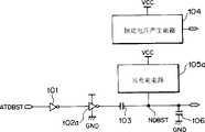
在第一实施例的升压电路中,升压启动信号ATDBST输入到反相器101的输入端,从升压节点NDBST(高电压输出端)输出电压Vboost,升压驱动器102的输入端接到反相器101的输出端,升压电容器103的一端接到升压驱动器102的输出端,升压驱动器102产生升压脉冲给升压电容103,升压节点NDBST接到升压电容103的另一端,升压节点NDBST接到高电压输出端(Vboost),接收升压脉冲的升压电容器将高电压输出端升压,升压电容器103的容值是Cb。In the boost circuit of the first embodiment, the boost start signal ATDBST is input to the input terminal of the
这里优选设置一接到高电压输出端的预充电电路105,用于在升压前的等待状态给高电压输出端(Vboost)提供电压。恒定电压Veonst作为电源输入给预充电电路105,预充电电路105的输出端接到升压节点NDBST。Here, a pre-charge circuit 105 connected to the high-voltage output terminal is preferably provided for providing voltage to the high-voltage output terminal (Vboost) in the waiting state before boosting. The constant voltage Veonst is input to the pre-charging circuit 105 as a power source, and the output terminal of the pre-charging circuit 105 is connected to the boost node NDBST.
进一步说,升压负载电容106可以接到升压节点NDBST,升压负载电容106的电容值是CL。Furthermore, the
升压电路优选具备给预充电电路105提供恒定电压的恒定电压产生电路104,电源电压VCC提供给恒定电压产生电路104,而恒定电压产生电路104的输出端输出恒定电压Vconst。The boost circuit preferably includes a constant
下面将描述用于第一实施例升压电路的预充电电路。图3是说明预充电电路105结构的电路图。Next, a precharge circuit used in the voltage boosting circuit of the first embodiment will be described. FIG. 3 is a circuit diagram illustrating the structure of the precharge circuit 105. As shown in FIG.
预充电电路105可具备反相器206,升压启动信号ATDBST从反相器206的输入端输入。反相器207的输入端和N-沟道MOS晶体管204的栅极连接到反相器206的输出端,N-沟道MOS晶体管205栅极接到反相器207的输出端。The precharge circuit 105 may include an
N-沟道MOS晶体管204的源极接地电位,P-沟道MOS晶体管201的漏极、P-沟道MOS晶体管202的栅极和P-沟道MOS晶体管203的栅极与N-沟道MOS晶体管204的漏极连接。The source ground potential of N-
N-沟道MOS晶体管205的源极接到地电位,P-沟道MOS晶体管202的漏极和P-沟道MOS晶体管201的栅极连接到N-沟道MOS晶体管205的漏极。The source of the N-
P-沟道MOS晶体管203的源极接恒定电压Vconst,P-沟道MOS晶体管203的漏极接升压节点NDBST。The source of the P-channel MOS transistor 203 is connected to the constant voltage Vconst, and the drain of the P-channel MOS transistor 203 is connected to the boost node NDBST.
升压节点NDBST接到P-沟道MOS晶体管201和202的源极。The boost node NDBST is connected to the sources of the P-
下面将描述用于第一实施例升压电路的升压驱动器102。图4是说明升压驱动器102结构的电路图。The boost driver 102 used in the boost circuit of the first embodiment will be described below. FIG. 4 is a circuit diagram illustrating the structure of the boost driver 102 .
升压驱动器102可具备P-沟道MOS晶体管301,升压启动信号的反相信号BSTIN从P-沟道MOS晶体管301的栅极输入,P-沟道MOS晶体管301的源极接到电源电压VCC,P-沟道MOS晶体管301的漏极接到升压脉冲产生节点BOOST。The boost driver 102 may have a P-
升压驱动器102也可具备N-沟道MOS晶体管302,升压启动信号的反相信号BSTIN从N-沟道MOS晶体管302的栅极输入,N-沟道MOS晶体管302的源极接到地电位,N-沟道MOS晶体管302的漏极接到升压脉冲产生节点BOOST。The boost driver 102 may also be equipped with an N-
下面将描述上述构成的第一实施例升压电路的操作。The operation of the booster circuit of the first embodiment constructed as above will be described below.
在升压前等待状态,升压启动信号ATDBST以低电平输入给反相器101,反相器101将升压启动信号ATDBST的电平反相,并且高电平信号VCC输入到升压驱动器102的输入端。In the waiting state before boosting, the boost start signal ATDBST is input to the
因此,升压驱动器102的输出信号维持低电平,这个低电平信号被输入到升压电容器103的一端。此时,恒定电压产生电路104提供的电压Vconst通过预充电电路105到达升压节点NDBST,并且电荷存入升压电容103和升压负载电容106。Therefore, the output signal of the boost driver 102 maintains a low level, and this low level signal is input to one terminal of the
当从此状态开始升压时,升压启动信号ATDBST从低电平转换为高电平VCC,并输入到反相器101的输入端。When boosting is started from this state, the boost start signal ATDBST is switched from a low level to a high level VCC, and is input to the input terminal of the
因此,反相器101的输出信号从高电平VCC转换为低电平,升压驱动器102的输出信号从低电平转换为高电平VCC。Therefore, the output signal of the
因此,高电平VCC信号提供给升压电容器103的一端,当高电平信号VCC提供给升压电容器103的一端时,升压节点NDBST从预充电电平Vconst升高到等式(2)所示的由升压电容103耦合的电压值。Therefore, a high-level VCC signal is supplied to one end of the boosting
Vboost=Vconst+(Cb/(Cb+CL))×VCC …(2)Vboost=Vconst+(Cb/(Cb+CL))×VCC …(2)
在等式(2)中,Vboost是从高电压输出端输出的电压,Vconst是从恒定电压产生电路104输出的恒定电压,Cb是升压电容器103的电容值,CL是升压负载电容器106的电容值,VCC是提供给恒定电压产生电路104的电源电压。In equation (2), Vboost is the voltage output from the high voltage output terminal, Vconst is the constant voltage output from the constant
当升压完成时,升压启动信号ATDBST的输入电平从高电平转换为低电平。因此,各节点的电压值回到升压启动前的电压值,升压过程结束。When the boost is completed, the input level of the boost start signal ATDBST is changed from high level to low level. Therefore, the voltage value of each node returns to the voltage value before the boost start, and the boost process ends.
如上所述,根据第一实施例,由于在升压前等待状态的预充电电平为不取决于电源电压的恒定电压,因此容易控制升压值到达上限。As described above, according to the first embodiment, since the precharge level in the standby state before boosting is a constant voltage that does not depend on the power supply voltage, it is easy to control the boosted value to the upper limit.
下面将描述本发明第二实施例。图5是说明本发明第二实施例升压电路的框图。Next, a second embodiment of the present invention will be described. Fig. 5 is a block diagram illustrating a second embodiment of a voltage boosting circuit of the present invention.
在第二实施例的升压电路中,升压启动信号ATDBST输入到反相器101的输入端,从升压节点NDBST(高电压输出端)输出电压Vboost,升压驱动器102a的输入端优选接到反相器101的输出端,升压电容器103的一端接到升压驱动器102a的输出端,从升压驱动器102a产生升压脉冲给升压电容器103,升压节点NDBST接到升压电容器103的另一端,升压节点NDBST接到高电压输出端(Vboost),升压电容器103接收升压脉冲,将高电压输出端升压,升压电容器103的电容值是Cb。In the boost circuit of the second embodiment, the boost start signal ATDBST is input to the input terminal of the
提供的预充电电路105a接到高电压输出端,用于在升压前的等待状态给高电压输出端(Vboost)提供电压,电源电压VCC作为电源输入给预充电电路105a,预充电电路105a的输出端接到升压节点NDBST。The provided pre-charging circuit 105a is connected to the high-voltage output terminal, and is used to provide voltage to the high-voltage output terminal (Vboost) in the waiting state before boosting, and the power supply voltage VCC is used as a power input to the pre-charging circuit 105a. The output terminal is connected to boost node NDBST.
进一步说,升压负载电容器106接到升压节点NDBST,升压负载电容器106电容值是CL。Furthermore, the
升压电路优选设置有恒定电压产生电路104,用于给升压驱动器102a提供恒定电压值Vconst,电源电压VCC提供给恒定电压产生电路104,从恒定电压产生电路104的输出端输出恒定电压Vconst。The boost circuit is preferably provided with a constant
下面将说明预充电电路105a和用于第二实施例升压电路的升压驱动器102a。图6是说明预充电电路105a的电路图,图7是说明升压驱动电路102a结构的电路图。在图6所示的预充电电路105a中或在图7所示的升压驱动电路102a中,与图3或图4中所示的预充电电路105a或升压驱动电路102a相似的元件用相同的参考标号表示,并省略对它们的详述。Next, the precharge circuit 105a and the
如图6所示,在第二实施例中使用的预充电电路105a,优选设置有源极接到电源电压VCC的P-沟道MOS晶体管203a,取代源极接到恒定电压Vconst的晶体管203。As shown in FIG. 6, the precharge circuit 105a used in the second embodiment is preferably provided with a P-
进一步说,如图7所示,在第二实施例中使用的升压电路102a优先具备源极接到恒定电压Vconst的P-沟道MOS晶体管301a,取代源极接到电源电压VCC的晶体管301。Further, as shown in FIG. 7, the
以下将描述上述结构的第二实施例升压电路的操作。The operation of the booster circuit of the second embodiment constructed as described above will be described below.
在升压前的等待状态,升压启动信号ATDBST以低电平输入到反相器101,反相器101将升压启动信号ATDBST的电平反相,高电平VCC信号输入到升压驱动器102a输入端。In the waiting state before boosting, the boost start signal ATDBST is input to the
因此,升压驱动器102a的输出信号维持在低电平,并且该低电平信号被输入到升压电容器103的一端,此时,电源电压VCC通过预充电电路105a达到升压节点NDBST,并且电荷存入升压电容器103和升压负载电容器106。Therefore, the output signal of the
当从该状态开始升压时,升压启动信号ATDBST从低电平转换为高电平VCC,并输入到反相器101的输入端。When boosting is started from this state, the boost start signal ATDBST is switched from low level to high level VCC, and is input to the input terminal of the
因此,反相器101的输出信号从高电平VCC转换为低电平,升压驱动器102a的输出信号从低电平转换为高电平Vconst。Therefore, the output signal of the
因此,高电平Vconst信号提供给升压电容103的一端,当高电平Vconst信号提供给升压电容103的一端时,升压节点NDBST从预充电电平VCC升高到等式(3)所示的由升压电容103耦合的电压值。Therefore, the high-level Vconst signal is supplied to one end of the
Vboost=VCC+(Cb/(Cb+CL))×Vconst …(3)Vboost=VCC+(Cb/(Cb+CL))×Vconst ...(3)
在等式(3)中,Vboost是从高电压输出端输出的电压,Vconst是从恒定电压产生电路104输出的恒定电压,Cb是升压电容器103的电容值,CL是升压负载电容器106的电容值,VCC是提供给恒定电压产生电路104的电源电压。In equation (3), Vboost is the voltage output from the high voltage output terminal, Vconst is the constant voltage output from the constant
当升压完成时,升压启动信号ATDBST的输入从高电平转换为低电平。因此,各节点的电压值回到升压启动时的电平,升压过程结束。When the boost is completed, the input of the boost start signal ATDBST is switched from high level to low level. Therefore, the voltage value of each node returns to the level when the boost is started, and the boost process ends.
如上所述,根据第二实施例,由于升压脉冲幅值是不取决于电源电压的恒定电压,因此容易控制升压值达到上限。As described above, according to the second embodiment, since the boost pulse amplitude is a constant voltage that does not depend on the power supply voltage, it is easy to control the boost value to the upper limit.
尽管在第一实施例中恒定电压产生电路104给预充电电路105提供恒定电压,而在第二实施例中恒定电压产生电路104给升压电路102a提供恒定电压,但本发明不限于这样的结构。Although the constant
例如,来自恒定电压产生电路的恒定电压可以提供给预充电电路和升压驱动器,在这种情况下,优选构成如图3所示的预充电电路,在升压前的等待状态,预充电电路给高电压输出端(Vboost)提供恒定电压,升压驱动器优选如图7所示构成,从升压驱动器产生的升压脉冲提供给升压电容。接收升压脉冲信号的升压电容器将高电压输出端升压。在这种情况下,升压前等待状态的预充电电平和升压脉冲的幅值是不取决于电源电压的恒定电压。For example, the constant voltage from the constant voltage generation circuit can be supplied to the precharge circuit and the boost driver. In this case, it is preferable to constitute the precharge circuit as shown in FIG. 3. In the waiting state before boosting, the precharge circuit To provide a constant voltage to the high voltage output terminal (Vboost), the boost driver is preferably configured as shown in FIG. 7, and the boost pulse generated from the boost driver is supplied to the boost capacitor. The boost capacitor receiving the boost pulse signal boosts the high voltage output terminal. In this case, the precharge level in the standby state before boosting and the amplitude of the boosting pulse are constant voltages that do not depend on the power supply voltage.
Claims (8)
Applications Claiming Priority (2)
| Application Number | Priority Date | Filing Date | Title |
|---|---|---|---|
| JP109200/98 | 1998-04-20 | ||
| JP10920098AJPH11308855A (en) | 1998-04-20 | 1998-04-20 | Boosting circuit |
Publications (1)
| Publication Number | Publication Date |
|---|---|
| CN1233058Atrue CN1233058A (en) | 1999-10-27 |
Family
ID=14504161
Family Applications (1)
| Application Number | Title | Priority Date | Filing Date |
|---|---|---|---|
| CN99105833APendingCN1233058A (en) | 1998-04-20 | 1999-04-20 | boost circuit |
Country Status (6)
| Country | Link |
|---|---|
| US (2) | US6268761B1 (en) |
| EP (1) | EP0952662A3 (en) |
| JP (1) | JPH11308855A (en) |
| KR (1) | KR100336254B1 (en) |
| CN (1) | CN1233058A (en) |
| TW (1) | TW422981B (en) |
Cited By (3)
| Publication number | Priority date | Publication date | Assignee | Title |
|---|---|---|---|---|
| CN101295536B (en)* | 2007-04-24 | 2011-08-17 | 南亚科技股份有限公司 | Boost circuit and its memory structure |
| CN101620886B (en)* | 2008-07-02 | 2012-01-25 | 中芯国际集成电路制造(上海)有限公司 | Word line supercharger for flash memory |
| CN109804326A (en)* | 2016-10-12 | 2019-05-24 | 赛普拉斯半导体公司 | Fast slope low-power-supply charge pump circuit |
Families Citing this family (15)
| Publication number | Priority date | Publication date | Assignee | Title |
|---|---|---|---|---|
| JP2002032987A (en)* | 2000-07-18 | 2002-01-31 | Mitsubishi Electric Corp | Internal voltage generation circuit |
| US6570434B1 (en)* | 2000-09-15 | 2003-05-27 | Infineon Technologies Ag | Method to improve charge pump reliability, efficiency and size |
| US6404273B1 (en)* | 2000-10-26 | 2002-06-11 | Stmicroelectronics S.R.L. | Voltage booster with a low output resistance |
| JP2003091997A (en)* | 2001-09-19 | 2003-03-28 | Seiko Epson Corp | Nonvolatile semiconductor memory device |
| KR100425474B1 (en)* | 2001-11-21 | 2004-03-30 | 삼성전자주식회사 | Data output method and data output circuit for applying reduced precharge level |
| ITVA20020017A1 (en)* | 2002-02-21 | 2003-08-21 | St Microelectronics Srl | VOLTAGE ELEVATOR INTEGRATED CIRCUIT WITH CHARGE PUMP |
| US7233194B2 (en)* | 2003-01-06 | 2007-06-19 | Texas Instruments Incorporated | CMOS voltage booster circuits |
| US6909318B2 (en)* | 2003-01-06 | 2005-06-21 | Texas Instruments Incorporated | CMOS voltage booster circuit |
| JP4149415B2 (en) | 2004-05-31 | 2008-09-10 | 株式会社ケーヒン | Boost power supply control device and failure site identification method for boost power supply control device |
| US7767844B2 (en) | 2005-05-23 | 2010-08-03 | Atomic Energy Council | Method for manufacturing diethylene triamine pentaacetic acid derivative |
| KR100803364B1 (en)* | 2006-11-13 | 2008-02-13 | 주식회사 하이닉스반도체 | Pumping Voltage Generation Circuit of Semiconductor Memory Device |
| US7847621B2 (en)* | 2007-11-13 | 2010-12-07 | Rohm Co., Ltd. | Control circuit and control method for charge pump circuit |
| JP2011034658A (en) | 2009-08-06 | 2011-02-17 | Fujitsu Semiconductor Ltd | Semiconductor memory device, boosting method of word line, and system |
| KR102509328B1 (en)* | 2016-08-29 | 2023-03-15 | 에스케이하이닉스 주식회사 | Apparatus for Voltage Switching and Semiconductor Memory Apparatus Having the Same |
| CN111262431B (en)* | 2020-03-18 | 2021-03-30 | 一汽解放汽车有限公司 | Boost control circuit and method for vehicle |
Family Cites Families (9)
| Publication number | Priority date | Publication date | Assignee | Title |
|---|---|---|---|---|
| US4736121A (en)* | 1985-09-10 | 1988-04-05 | Sos Microelettronica S.p.A. | Charge pump circuit for driving N-channel MOS transistors |
| JPH0697836B2 (en) | 1987-05-20 | 1994-11-30 | 松下電器産業株式会社 | Boost circuit |
| IT1258242B (en)* | 1991-11-07 | 1996-02-22 | Samsung Electronics Co Ltd | SEMICONDUCTOR MEMORY DEVICE INCLUDING SUPPLY VOLTAGE PUMPING CIRCUIT |
| JPH0660651A (en) | 1992-07-31 | 1994-03-04 | Sony Corp | Step-up circuit and step-up method |
| JP3190940B2 (en) | 1993-05-31 | 2001-07-23 | 松下電子工業株式会社 | Boost circuit |
| US5629843A (en)* | 1993-10-15 | 1997-05-13 | Micron Technology, Inc. | Self compensating clamp circuit and method for limiting a potential at a pump circuit node |
| JPH09320267A (en)* | 1996-05-28 | 1997-12-12 | Oki Micro Design Miyazaki:Kk | Boosting circuit driving method and boosting circuit |
| KR100200721B1 (en)* | 1996-08-20 | 1999-06-15 | 윤종용 | Internal vpp generator of semiconductor memory device |
| US5767729A (en)* | 1996-10-31 | 1998-06-16 | Integrated Silicon Solution Inc. | Distribution charge pump for nonvolatile memory device |
- 1998
- 1998-04-20JPJP10920098Apatent/JPH11308855A/enactivePending
- 1999
- 1999-04-12USUS09/289,596patent/US6268761B1/ennot_activeExpired - Fee Related
- 1999-04-19EPEP99107772Apatent/EP0952662A3/ennot_activeWithdrawn
- 1999-04-20KRKR1019990013954Apatent/KR100336254B1/ennot_activeExpired - Fee Related
- 1999-04-20CNCN99105833Apatent/CN1233058A/enactivePending
- 1999-04-20TWTW088106398Apatent/TW422981B/ennot_activeIP Right Cessation
- 2001
- 2001-04-27USUS09/842,711patent/US20010019286A1/ennot_activeAbandoned
Cited By (3)
| Publication number | Priority date | Publication date | Assignee | Title |
|---|---|---|---|---|
| CN101295536B (en)* | 2007-04-24 | 2011-08-17 | 南亚科技股份有限公司 | Boost circuit and its memory structure |
| CN101620886B (en)* | 2008-07-02 | 2012-01-25 | 中芯国际集成电路制造(上海)有限公司 | Word line supercharger for flash memory |
| CN109804326A (en)* | 2016-10-12 | 2019-05-24 | 赛普拉斯半导体公司 | Fast slope low-power-supply charge pump circuit |
Also Published As
| Publication number | Publication date |
|---|---|
| EP0952662A3 (en) | 2002-02-06 |
| US6268761B1 (en) | 2001-07-31 |
| TW422981B (en) | 2001-02-21 |
| EP0952662A2 (en) | 1999-10-27 |
| JPH11308855A (en) | 1999-11-05 |
| KR19990083335A (en) | 1999-11-25 |
| US20010019286A1 (en) | 2001-09-06 |
| KR100336254B1 (en) | 2002-05-09 |
Similar Documents
| Publication | Publication Date | Title |
|---|---|---|
| CN1233058A (en) | boost circuit | |
| CN1125467C (en) | Nonvolatile memory device having flash EEPROM cells | |
| CN1267928C (en) | Semiconductor memory device with control for auxiliary word lines for memory cell selection | |
| CN1168095C (en) | High density NOR type flash memory device and programming method thereof | |
| JP2652694B2 (en) | Boost circuit | |
| CN1832040A (en) | Flash memory device with improved erase function and method for controlling erase operation of the same | |
| US8717816B2 (en) | Semiconductor memory device | |
| US7626865B2 (en) | Charge pump operation in a non-volatile memory device | |
| CN1229998A (en) | Semiconductor device | |
| CN1280413A (en) | boost circuit | |
| CN1245338A (en) | Semiconductor memory | |
| CN1674155A (en) | Power supply circuit and semiconductor storage device with the power supply circuit | |
| EP1255255B1 (en) | High speed decoder for flash memory | |
| CN1237767A (en) | Semiconductor memory device | |
| CN1801397A (en) | Semiconductor memory device | |
| US4905314A (en) | Semiconductor integrated circuit device having an object circuit to which output voltages of the sub- and main booster circuits are applied | |
| CN1090407C (en) | Mode setting circuit and mode setting apparatus | |
| CN1116684C (en) | Word line driver, memory using same and method for reducing power consumption of voltage source | |
| CN1921012A (en) | Circuit for generating step-up voltage in non-volatile memory device | |
| JPH0628876A (en) | Nonvolatile semiconductor memory device | |
| CN1234171C (en) | Semiconductor memory and voltage application method to semiconductor memory | |
| CN1734664A (en) | Ferroelectric memory device and electronic equipment | |
| US8593874B2 (en) | Voltage generation circuit which is capable of reducing circuit area | |
| CN1577621A (en) | Data erasing method, and memory apparatus having data erasing circuit using such method | |
| KR100355089B1 (en) | Power supply circuit |
Legal Events
| Date | Code | Title | Description |
|---|---|---|---|
| C10 | Entry into substantive examination | ||
| SE01 | Entry into force of request for substantive examination | ||
| C06 | Publication | ||
| PB01 | Publication | ||
| ASS | Succession or assignment of patent right | Owner name:NEC ELECTRONICS TAIWAN LTD. Free format text:FORMER OWNER: NIPPON ELECTRIC CO., LTD. Effective date:20030530 | |
| C41 | Transfer of patent application or patent right or utility model | ||
| TA01 | Transfer of patent application right | Effective date of registration:20030530 Address after:Kanagawa, Japan Applicant after:NEC Corp. Address before:Tokyo, Japan Applicant before:NEC Corp. | |
| C02 | Deemed withdrawal of patent application after publication (patent law 2001) | ||
| WD01 | Invention patent application deemed withdrawn after publication |