CN1231970C - Semiconductor device - Google Patents
Semiconductor deviceDownload PDFInfo
- Publication number
- CN1231970C CN1231970CCNB021575487ACN02157548ACN1231970CCN 1231970 CCN1231970 CCN 1231970CCN B021575487 ACNB021575487 ACN B021575487ACN 02157548 ACN02157548 ACN 02157548ACN 1231970 CCN1231970 CCN 1231970C
- Authority
- CN
- China
- Prior art keywords
- wiring
- connecting hole
- dummy
- semiconductor device
- film
- Prior art date
- Legal status (The legal status is an assumption and is not a legal conclusion. Google has not performed a legal analysis and makes no representation as to the accuracy of the status listed.)
- Expired - Fee Related
Links
Images


Classifications
- H—ELECTRICITY
- H01—ELECTRIC ELEMENTS
- H01L—SEMICONDUCTOR DEVICES NOT COVERED BY CLASS H10
- H01L21/00—Processes or apparatus adapted for the manufacture or treatment of semiconductor or solid state devices or of parts thereof
- H01L21/02—Manufacture or treatment of semiconductor devices or of parts thereof
- H01L21/04—Manufacture or treatment of semiconductor devices or of parts thereof the devices having potential barriers, e.g. a PN junction, depletion layer or carrier concentration layer
- H01L21/18—Manufacture or treatment of semiconductor devices or of parts thereof the devices having potential barriers, e.g. a PN junction, depletion layer or carrier concentration layer the devices having semiconductor bodies comprising elements of Group IV of the Periodic Table or AIIIBV compounds with or without impurities, e.g. doping materials
- H01L21/30—Treatment of semiconductor bodies using processes or apparatus not provided for in groups H01L21/20 - H01L21/26
- H01L21/31—Treatment of semiconductor bodies using processes or apparatus not provided for in groups H01L21/20 - H01L21/26 to form insulating layers thereon, e.g. for masking or by using photolithographic techniques; After treatment of these layers; Selection of materials for these layers
- H01L21/3205—Deposition of non-insulating-, e.g. conductive- or resistive-, layers on insulating layers; After-treatment of these layers
- H—ELECTRICITY
- H01—ELECTRIC ELEMENTS
- H01L—SEMICONDUCTOR DEVICES NOT COVERED BY CLASS H10
- H01L21/00—Processes or apparatus adapted for the manufacture or treatment of semiconductor or solid state devices or of parts thereof
- H01L21/70—Manufacture or treatment of devices consisting of a plurality of solid state components formed in or on a common substrate or of parts thereof; Manufacture of integrated circuit devices or of parts thereof
- H01L21/71—Manufacture of specific parts of devices defined in group H01L21/70
- H01L21/768—Applying interconnections to be used for carrying current between separate components within a device comprising conductors and dielectrics
- H01L21/76801—Applying interconnections to be used for carrying current between separate components within a device comprising conductors and dielectrics characterised by the formation and the after-treatment of the dielectrics, e.g. smoothing
- H01L21/76802—Applying interconnections to be used for carrying current between separate components within a device comprising conductors and dielectrics characterised by the formation and the after-treatment of the dielectrics, e.g. smoothing by forming openings in dielectrics
- H01L21/76807—Applying interconnections to be used for carrying current between separate components within a device comprising conductors and dielectrics characterised by the formation and the after-treatment of the dielectrics, e.g. smoothing by forming openings in dielectrics for dual damascene structures
- H01L21/76811—Applying interconnections to be used for carrying current between separate components within a device comprising conductors and dielectrics characterised by the formation and the after-treatment of the dielectrics, e.g. smoothing by forming openings in dielectrics for dual damascene structures involving multiple stacked pre-patterned masks
- H—ELECTRICITY
- H01—ELECTRIC ELEMENTS
- H01L—SEMICONDUCTOR DEVICES NOT COVERED BY CLASS H10
- H01L21/00—Processes or apparatus adapted for the manufacture or treatment of semiconductor or solid state devices or of parts thereof
- H01L21/70—Manufacture or treatment of devices consisting of a plurality of solid state components formed in or on a common substrate or of parts thereof; Manufacture of integrated circuit devices or of parts thereof
- H01L21/71—Manufacture of specific parts of devices defined in group H01L21/70
- H01L21/768—Applying interconnections to be used for carrying current between separate components within a device comprising conductors and dielectrics
- H01L21/76801—Applying interconnections to be used for carrying current between separate components within a device comprising conductors and dielectrics characterised by the formation and the after-treatment of the dielectrics, e.g. smoothing
- H01L21/76802—Applying interconnections to be used for carrying current between separate components within a device comprising conductors and dielectrics characterised by the formation and the after-treatment of the dielectrics, e.g. smoothing by forming openings in dielectrics
- H01L21/76807—Applying interconnections to be used for carrying current between separate components within a device comprising conductors and dielectrics characterised by the formation and the after-treatment of the dielectrics, e.g. smoothing by forming openings in dielectrics for dual damascene structures
- H01L21/76813—Applying interconnections to be used for carrying current between separate components within a device comprising conductors and dielectrics characterised by the formation and the after-treatment of the dielectrics, e.g. smoothing by forming openings in dielectrics for dual damascene structures involving a partial via etch
- H—ELECTRICITY
- H01—ELECTRIC ELEMENTS
- H01L—SEMICONDUCTOR DEVICES NOT COVERED BY CLASS H10
- H01L21/00—Processes or apparatus adapted for the manufacture or treatment of semiconductor or solid state devices or of parts thereof
- H01L21/70—Manufacture or treatment of devices consisting of a plurality of solid state components formed in or on a common substrate or of parts thereof; Manufacture of integrated circuit devices or of parts thereof
- H01L21/71—Manufacture of specific parts of devices defined in group H01L21/70
- H01L21/768—Applying interconnections to be used for carrying current between separate components within a device comprising conductors and dielectrics
- H01L21/76838—Applying interconnections to be used for carrying current between separate components within a device comprising conductors and dielectrics characterised by the formation and the after-treatment of the conductors
- H01L21/7684—Smoothing; Planarisation
- H—ELECTRICITY
- H01—ELECTRIC ELEMENTS
- H01L—SEMICONDUCTOR DEVICES NOT COVERED BY CLASS H10
- H01L23/00—Details of semiconductor or other solid state devices
- H01L23/52—Arrangements for conducting electric current within the device in operation from one component to another, i.e. interconnections, e.g. wires, lead frames
- H01L23/522—Arrangements for conducting electric current within the device in operation from one component to another, i.e. interconnections, e.g. wires, lead frames including external interconnections consisting of a multilayer structure of conductive and insulating layers inseparably formed on the semiconductor body
- H01L23/5226—Via connections in a multilevel interconnection structure
- H—ELECTRICITY
- H01—ELECTRIC ELEMENTS
- H01L—SEMICONDUCTOR DEVICES NOT COVERED BY CLASS H10
- H01L23/00—Details of semiconductor or other solid state devices
- H01L23/52—Arrangements for conducting electric current within the device in operation from one component to another, i.e. interconnections, e.g. wires, lead frames
- H01L23/522—Arrangements for conducting electric current within the device in operation from one component to another, i.e. interconnections, e.g. wires, lead frames including external interconnections consisting of a multilayer structure of conductive and insulating layers inseparably formed on the semiconductor body
- H01L23/528—Layout of the interconnection structure
- H01L23/5283—Cross-sectional geometry
- H—ELECTRICITY
- H01—ELECTRIC ELEMENTS
- H01L—SEMICONDUCTOR DEVICES NOT COVERED BY CLASS H10
- H01L2221/00—Processes or apparatus adapted for the manufacture or treatment of semiconductor or solid state devices or of parts thereof covered by H01L21/00
- H01L2221/10—Applying interconnections to be used for carrying current between separate components within a device
- H01L2221/1005—Formation and after-treatment of dielectrics
- H01L2221/101—Forming openings in dielectrics
- H01L2221/1015—Forming openings in dielectrics for dual damascene structures
- H01L2221/1036—Dual damascene with different via-level and trench-level dielectrics
- H—ELECTRICITY
- H01—ELECTRIC ELEMENTS
- H01L—SEMICONDUCTOR DEVICES NOT COVERED BY CLASS H10
- H01L2924/00—Indexing scheme for arrangements or methods for connecting or disconnecting semiconductor or solid-state bodies as covered by H01L24/00
- H01L2924/0001—Technical content checked by a classifier
- H01L2924/0002—Not covered by any one of groups H01L24/00, H01L24/00 and H01L2224/00
Landscapes
- Engineering & Computer Science (AREA)
- Physics & Mathematics (AREA)
- Condensed Matter Physics & Semiconductors (AREA)
- General Physics & Mathematics (AREA)
- Computer Hardware Design (AREA)
- Microelectronics & Electronic Packaging (AREA)
- Power Engineering (AREA)
- Manufacturing & Machinery (AREA)
- Geometry (AREA)
- Internal Circuitry In Semiconductor Integrated Circuit Devices (AREA)
Abstract
Translated fromChineseDescription
Translated fromChinese技术领域technical field
本发明涉及一种半导体器件,特别涉及一种通过镶嵌处理而制造的半导体器件。The present invention relates to a semiconductor device, in particular to a semiconductor device manufactured by damascene processing.
背景技术Background technique
最近几年,随着半导体器件的集成密度的提高,需要使布线小型化。作为形成该布线的方法,存在有在铝膜上形成阻挡金属层,然后通过直接对铝膜和阻挡金属层进行构图而形成铝布线的方法。根据该方法,由于在构图过程中在横向方向上对铝膜进行蚀刻,不但布线宽度不必要地被缩小,而且阻挡金属层保留在该铝布线上类似于单坡屋顶。按照这种方式,本发明在制造精确布线方面存在困难,并且限制布线的小型化。In recent years, as the integration density of semiconductor devices has increased, miniaturization of wiring has been required. As a method of forming this wiring, there is a method of forming a barrier metal layer on an aluminum film, and then forming an aluminum wiring by directly patterning the aluminum film and the barrier metal layer. According to this method, since the aluminum film is etched in the lateral direction during the patterning process, not only the wiring width is unnecessarily reduced, but also the barrier metal layer remains on the aluminum wiring like a lean-to roof. In this way, the present invention has difficulty in manufacturing accurate wiring and limits the miniaturization of wiring.
相反,在所谓的镶嵌处理中,金属膜不被如上文所述那样直接构图。而是通过蚀刻该绝缘膜而形成沟槽然后在该沟槽中掩埋例如铜这样的金属而形成该布线。由于蚀刻对象是绝缘膜,因此在镶嵌处理中不出现上述缺点,因此可以根据需要使该布线小型化。另外,由于具有比铝布线的电阻更低的电阻的铜布线可以在镶嵌处理中形成,因此可以增加半导体器件的工作速度。In contrast, in so-called damascene processing, the metal film is not directly patterned as described above. Instead, the wiring is formed by etching the insulating film to form a trench and then burying metal such as copper in the trench. Since the etching object is an insulating film, the above-mentioned disadvantages do not occur in the damascene process, so that the wiring can be miniaturized as necessary. In addition, since the copper wiring having a lower resistance than that of the aluminum wiring can be formed in the damascene process, the operating speed of the semiconductor device can be increased.
镶嵌处理大体上被分为两类,单一镶嵌处理和双重镶嵌处理。The mosaic processing is largely classified into two types, single mosaic processing and double mosaic processing.
图19为示出通过现有技术的单一镶嵌处理而制造的半导体器件。在图19中,参考标号3表示由阻挡金属层2和金属膜1所构成的第一布线。这种第一布线3被埋在绝缘膜12中的布线沟槽12a中。FIG. 19 is a diagram showing a semiconductor device manufactured by a conventional single damascene process. In FIG. 19 , reference numeral 3 denotes a first wiring composed of barrier metal layer 2 and
另一方面,参考标号8表示由阻挡金属层6和金属膜7所构成的第二布线,并且被埋在上绝缘膜5的布线沟槽5a中。该第二布线8和上述第一布线3通过导电插塞(在下文中被称为“插塞”)11被电连接。这种插塞11具有由阻挡金属层9和金属膜10所构成的双层结构,并且被埋在下绝缘膜4中的通孔4a内。On the other hand, reference numeral 8 denotes a second wiring composed of barrier metal layer 6 and
为了通过单一镶嵌处理而获得上述结构,在形成下绝缘膜4之后,把插塞11埋在该通孔4a中。然后,在下绝缘膜4上形成上绝缘膜5,然后在上绝缘膜5中形成布线沟槽5a。然后,连接到插塞11的第二布线8被埋在布线沟槽5a中。In order to obtain the above structure by a single damascene process, after the lower insulating film 4 is formed, the plug 11 is buried in the via hole 4a. Then, an upper insulating film 5 is formed on the lower insulating film 4 , and then a wiring trench 5 a is formed in the upper insulating film 5 . Then, the second wiring 8 connected to the plug 11 is buried in the wiring trench 5a.
按照这种方式,由于在单一镶嵌处理中分别形成插塞11和第二布线8,形成这样一种结构,使得金属膜10和金属膜7由阻挡金属层6所绝缘。In this way, since the plug 11 and the second wiring 8 are formed separately in a single damascene process, a structure is formed such that the metal film 10 and the
另一方面,图20为通过现有技术中的双重镶嵌处理而制造的半导体器件的截面视图。在图20中,与图19相同的参考标号表示与图9中相同的构成部件,并且将省略对它们的描述。On the other hand, FIG. 20 is a cross-sectional view of a semiconductor device manufactured by a dual damascene process in the prior art. In FIG. 20 , the same reference numerals as in FIG. 19 denote the same constituent elements as in FIG. 9 , and descriptions thereof will be omitted.
为了通过双重镶嵌处理获得该结构,下绝缘膜4和上绝缘膜5被叠加,然后在这些绝缘膜中形成布线沟槽5a和通孔4a。然后,同时在布线沟槽5a和通孔4a的内壁上形成阻挡金属层13。然后,通过在阻挡金属层13上形成金属膜14而同时形成插塞11和第二布线8。插塞11和第二布线8具有阻挡金属层13和金属膜14的双层结构。In order to obtain this structure by the dual damascene process, lower insulating film 4 and upper insulating film 5 are laminated, and then wiring trench 5a and via hole 4a are formed in these insulating films. Then, the barrier metal layer 13 is formed on the inner walls of the wiring trench 5a and the via hole 4a at the same time. Then, the plug 11 and the second wiring 8 are simultaneously formed by forming the metal film 14 on the barrier metal layer 13 . The plug 11 and the second wiring 8 have a two-layer structure of a barrier metal layer 13 and a metal film 14 .
按照这种方式,在双重镶嵌处理中,同时形成插塞11和第二布线8。结果,不是通过阻挡金属层而绝缘插塞11和第二布线8,而是整体地形成该插塞和第二布线。In this way, in the dual damascene process, the plug 11 and the second wiring 8 are formed at the same time. As a result, instead of insulating the plug 11 and the second wiring 8 by the barrier metal layer, the plug and the second wiring 8 are integrally formed.
如上文所述,单一和双重镶嵌处理可以使布线小型化,并且提高半导体器件的集成密度。As described above, single and dual damascene processing can miniaturize wiring and increase the integration density of semiconductor devices.
但是,这种半导体器件仍然要改进其抗应力迁移性。该应力迁移是这样一种现象,其中由于在金属膜14和绝缘体(上绝缘膜或下绝缘膜)之间的热膨胀系数等等这样的物理常数的差别而导致金属膜14(在一些情况中为阻挡金属层13)在通孔4a中提升(lifted up),而造成插塞11和第一布线3之间接触不良。However, such semiconductor devices still need to be improved in their resistance to stress migration. This stress migration is a phenomenon in which the metal film 14 (in some cases, The barrier metal layer 13) is lifted up in the via hole 4a, causing poor contact between the plug 11 and the first wiring 3.
如果按照这种方式容易出现应力迁移,则在制造过程中的热处理中增加废品率,这导致增加半导体器件的制造成本的缺点。If stress migration tends to occur in this way, the reject rate increases in heat treatment in the manufacturing process, which leads to a disadvantage of increasing the manufacturing cost of the semiconductor device.
发明内容Contents of the invention
本发明的一个目的是提供一种半导体器件,其相对于背景技术改进了抗应力迁移性。It is an object of the present invention to provide a semiconductor device having improved resistance to stress migration with respect to the background art.
上述目的可以通过提供一种半导体器件而实现,该半导体器件包括在第一布线的表面与第一绝缘膜的表面构成的一个平整表面上形成第二绝缘膜,以覆盖第一布线;在第二绝缘膜中形成的布线沟槽;在第二绝缘膜中形成的连接孔,以从该布线沟槽延伸到该第一布线;在第二绝缘膜中形成的伪连接孔,以从布线沟槽延伸到不形成第一布线的区域;第二布线,其被埋在该连接孔和布线沟槽中,以电连接到第一布线,并且还被埋在伪连接孔中,并且被形成为使得第二布线的表面与第一绝缘膜的表面构成一个平整的表面;以及形成在所述第二布线上方并电连接至第二布线的上部布线。The above objects can be achieved by providing a semiconductor device comprising forming a second insulating film on a flat surface formed by the surface of the first wiring and the surface of the first insulating film so as to cover the first wiring; a wiring trench formed in the insulating film; a connection hole formed in the second insulating film to extend from the wiring trench to the first wiring; a dummy connection hole formed in the second insulating film to extend from the wiring trench to the first wiring; extending to a region where the first wiring is not formed; the second wiring, which is buried in the connection hole and the wiring trench to be electrically connected to the first wiring, and is also buried in the dummy connection hole, and is formed such that A surface of the second wiring constitutes a flat surface with a surface of the first insulating film; and an upper wiring formed over the second wiring and electrically connected to the second wiring.
众所周知,由于布线长度变得更长,因此在非通过镶嵌处理而是通过直接对铝膜构图而形成的铝布线中更加容易出现应力迁移。在本说明书中,布线长度被定义为在相同布线上两个相邻插塞的中央之间的距离(参见图20)。It is well known that stress migration is more likely to occur in aluminum wiring formed not by damascene processing but by directly patterning an aluminum film as the wiring length becomes longer. In this specification, the wiring length is defined as the distance between the centers of two adjacent plugs on the same wiring (see FIG. 20 ).
相反,在镶嵌处理中,按这种方式应力迁移表现出对布线长度的相关性是未知的。In contrast, in damascene processing, stress migration in this way exhibits an unknown dependence on wire length.
但是,本申请的发明人发现通过镶嵌处理形成的第二布线8还表现出对布线长度的相关性,并且当布线长度变得更长时容易出现应力迁移。特别地,本申请的发明人发现通过双重镶嵌处理所形成的布线与通过单一镶嵌处理所形成的布线相比容易造成应力迁移。However, the inventors of the present application found that the second wiring 8 formed by the damascene process also exhibits a dependence on the wiring length, and stress migration tends to occur when the wiring length becomes longer. In particular, the inventors of the present application found that wirings formed by dual damascene processing tend to cause stress migration compared to wirings formed by single damascene processing.
如图20中所示,这是因为插塞11和第二布线8被在双重镶嵌处理中整体地形成,因此插塞11的金属膜14容易被热应力而移动到第二布线8。这种情况在插塞11和第二布线8被阻挡金属层6所绝缘的单一镶嵌处理中不容易发生(参见图19)。As shown in FIG. 20 , this is because the plug 11 and the second wiring 8 are integrally formed in the dual damascene process, and thus the metal film 14 of the plug 11 is easily moved to the second wiring 8 by thermal stress. This situation does not easily occur in a single damascene process in which the plug 11 and the second wiring 8 are insulated by the barrier metal layer 6 (see FIG. 19 ).
根据本发明,被埋在第二绝缘膜中的连接孔内的第二布线的部分作为导电插塞。并且,被埋在第二绝缘膜中的伪连接孔内的第二布线的部分作为伪导电插塞。According to the present invention, the part of the second wiring buried in the connection hole in the second insulating film serves as the conductive plug. And, the part of the second wiring buried in the dummy connection hole in the second insulating film serves as a dummy conductive plug.
这些插塞(包括导电插塞和伪导电插塞)之间的位置关系在下文中讨论。应当指出,即使上述位置关系被替换为连接孔(包括连接孔和伪连接孔)之间的位置关系,上述论点仍然有效。The positional relationship between these plugs (including conductive plugs and dummy conductive plugs) is discussed below. It should be noted that even if the above-mentioned positional relationship is replaced by a positional relationship between connecting holes (including connecting holes and dummy connecting holes), the above argument is still valid.
根据本发明,通过提供伪导电插塞,最初被定义为相邻导电插塞之间的距离的第二布线的布线长度可以被缩短为伪导电插塞和导电插塞之间的距离。因此,当布线长度较长时频繁出现的应力迁移被减小。According to the present invention, by providing the dummy conductive plugs, the wiring length of the second wiring originally defined as the distance between adjacent conductive plugs can be shortened to the distance between the dummy conductive plugs and the conductive plugs. Therefore, stress migration, which occurs frequently when the wiring length is long, is reduced.
并且,根据该模拟结果,即使在连续的第二布线上仅仅提供一个导电插塞的情况中不能够定义第二布线的布线长度,显然把为导电插塞提供在导电插塞周围减小该应力迁移。And, from this simulation result, even if the wiring length of the second wiring cannot be defined in the case where only one conductive plug is provided on the continuous second wiring, it is apparent that providing the conductive plug around the conductive plug reduces the stress migrate.
另外,可以在不形成第一布线的区域中提供伪布线,并且可以形成在第二绝缘膜中的伪连接孔,以到达该伪布线。如果这样的话,伪导电插塞被连接到该伪布线。由于第二布线可以由使用伪布线作为基础的伪导电插塞牢固地支承,因此由第二绝缘膜和第二布线所构成的层叠体的机械强度可以得到增强。In addition, a dummy wiring may be provided in a region where the first wiring is not formed, and a dummy connection hole may be formed in the second insulating film to reach the dummy wiring. If so, a dummy conductive plug is connected to the dummy wiring. Since the second wiring can be firmly supported by the dummy conductive plug using the dummy wiring as a base, the mechanical strength of the laminated body composed of the second insulating film and the second wiring can be enhanced.
在提供伪布线的区域,最好使一个平面中的包括第一布线和伪布线的总布线占有率基本上为常量。如果这样的话,当执行CMP(化学机械抛光)时,在抛光之后的伪布线和第一布线的高度容易被控制。In the area where the dummy wiring is provided, it is preferable to make the total wiring occupancy rate in one plane including the first wiring and the dummy wiring substantially constant. If so, when CMP (Chemical Mechanical Polishing) is performed, the heights of dummy wirings and first wirings after polishing are easily controlled.
另外,当p1(即,相邻连接孔之间的间距)小于1微米时,可以良好地减小应力迁移。In addition, when p1 (ie, the distance between adjacent connection holes) is less than 1 μm, stress migration can be well reduced.
具体来说,当间距p1小于0.6微米时,可以更加有效地减小应力迁移。Specifically, when the pitch p1 is smaller than 0.6 μm, the stress migration can be reduced more effectively.
类似地,当相邻导电插塞和伪导电插塞之间的间距p1(即,相邻连接孔和伪连接孔之间的间距)被设置为小于1微米时,可以良好地减小应力迁移。Similarly, when the pitchp1 between adjacent conductive plugs and dummy conductive plugs (i.e., the pitch between adjacent connection holes and dummy connection holes) is set to be less than 1 μm, the stress can be well reduced migrate.
然后,当该间距p1被设置为小于0.6微米时,可以更加有效地减小应力迁移。Then, when the pitch p1 is set to be smaller than 0.6 μm, stress migration can be more effectively reduced.
在多个第二布线被设置在一个区域中的位置处,最好减小相邻第二布线之间的布线间电容。为此目的,被埋在一个第二布线中的导电插塞或伪导电插塞的一部分以及埋在其它第二布线中的导电插塞或伪导电插塞的一部分可以被设置为不在与两个相邻的第二布线的任何一个的延伸方向相垂直的方向上相互正对。由此,由于在相邻第二布线中的每个插塞(包括导电插塞和伪导电插塞)不被设置为相互针对,因此可以减小插塞之间的相对电容,因此可以避免由于相对电容所导致的第二布线之间的布线间电容的增加。At a position where a plurality of second wirings are provided in one area, it is preferable to reduce the inter-wiring capacitance between adjacent second wirings. For this purpose, a part of a conductive plug or a dummy conductive plug buried in one second wiring and a part of a conductive plug or a dummy conductive plug buried in the other second wiring may be arranged so as not to be in contact with the two The extension directions of any of the adjacent second wirings face each other in a direction perpendicular to each other. Thereby, since each plug (including the conductive plug and the dummy conductive plug) in the adjacent second wiring is not set against each other, the relative capacitance between the plugs can be reduced, thus avoiding the An increase in the inter-wiring capacitance between the second wirings due to the relative capacitance.
另外,用于覆盖第二布线的第三绝缘膜可以形成在第二布线上。在这种情况中,与在第二绝缘膜中相同,布线沟槽、连接孔以及伪连接孔被形成在第三绝缘膜中,并且第三布线被埋在它们中。In addition, a third insulating film for covering the second wiring may be formed on the second wiring. In this case, as in the second insulating film, wiring trenches, connection holes, and dummy connection holes are formed in the third insulating film, and third wirings are buried in them.
如果按照这种方式提供第三布线,则最好减小第三布线与第二布线之间的布线间电容。为此目的,从第三布线的上侧来看时,形成在第二布线中的导电插塞和伪导电插塞的一部分以及形成在第三布线中的导电插塞和伪导电插塞的一部分被设置为不在与第二布线和第三布线的任何一个延伸方向相垂直的方向上相互正对。由此,由于形成在不同布线(第二布线和第三布线)中的每个插塞(导电插塞和伪导电插塞)不被相邻设置,因此可以减小插塞之间的相对电容,由于可以避免相对电容,从而增加在第二布线与第三布线之间的布线间电容。If the third wiring is provided in this way, it is preferable to reduce the inter-wiring capacitance between the third wiring and the second wiring. For this purpose, when viewed from the upper side of the third wiring, a part of the conductive plug and dummy conductive plug formed in the second wiring and a part of the conductive plug and dummy conductive plug formed in the third wiring They are provided so as not to face each other in a direction perpendicular to any extending direction of the second wiring and the third wiring. Thus, since each plug (conductive plug and dummy conductive plug) formed in different wirings (second wiring and third wiring) is not adjacently disposed, the relative capacitance between the plugs can be reduced. , since the relative capacitance can be avoided, thereby increasing the inter-wiring capacitance between the second wiring and the third wiring.
然后,最好由聚芳醚材料所制成的薄膜的绝缘膜被用作为第一绝缘膜和第二绝缘膜。如果采用这种绝缘膜,则可以减小布线间电容,从而可以增加半导体器件的工作速度。Then, thin insulating films preferably made of polyarylene ether material are used as the first insulating film and the second insulating film. If such an insulating film is used, the inter-wiring capacitance can be reduced, so that the operating speed of the semiconductor device can be increased.
附图说明Description of drawings
图1为示出根据本发明第一实施例的截面示图;FIG. 1 is a cross-sectional view showing a first embodiment according to the present invention;
图2为示出根据本发明第一实施例的半导体器件的平面示图;2 is a plan view showing a semiconductor device according to a first embodiment of the present invention;
图3为示出根据本发明第二实施例的半导体器件的截面示图;3 is a cross-sectional view showing a semiconductor device according to a second embodiment of the present invention;
图4为示出根据本发明第二实施例的半导体器件的平面示图;4 is a plan view showing a semiconductor device according to a second embodiment of the present invention;
图5A至5C为示出根据本发明第三实施例的半导体器件的平面示图;5A to 5C are plan views showing a semiconductor device according to a third embodiment of the present invention;
图6为示出根据本发明第四实施例的半导体器件的平面示图;6 is a plan view showing a semiconductor device according to a fourth embodiment of the present invention;
图7为沿着图6的III-III线截取的截面示图;Fig. 7 is a sectional view taken along line III-III of Fig. 6;
图8为示出根据本发明第五实施例的半导体器件的截面示图;8 is a cross-sectional view showing a semiconductor device according to a fifth embodiment of the present invention;
图9为示出根据本发明第五实施例的半导体器件的平面示图;9 is a plan view showing a semiconductor device according to a fifth embodiment of the present invention;
图10为示出根据本发明第五实施例的另一个半导体器件的平面示图;10 is a plan view showing another semiconductor device according to a fifth embodiment of the present invention;
图11为示出沿着图10中的IV-IV线截取的截面示图;FIG. 11 is a cross-sectional view taken along line IV-IV in FIG. 10;
图12A至12N为示出制造根据本发明的实施例的半导体器件的方法的截面示图;12A to 12N are cross-sectional views illustrating a method of manufacturing a semiconductor device according to an embodiment of the present invention;
图13为示出在制造根据本发明的实施例的半导体器件的方法中,当布线密度存在极大差别时所造成的缺点的截面示图;13 is a cross-sectional view showing a disadvantage caused when there is a great difference in wiring density in a method of manufacturing a semiconductor device according to an embodiment of the present invention;
图14为示出在制造根据本发明的实施例的半导体器件的方法中,形成四层布线的情况的截面示图;14 is a cross-sectional view showing a case where four-layer wiring is formed in a method of manufacturing a semiconductor device according to an embodiment of the present invention;
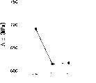
图15A为示出根据本发明第一实施例的半导体器件的第一模拟结果的曲线图,以及图15B为示出用于该模拟中的模型的截面示图;15A is a graph showing a first simulation result of the semiconductor device according to the first embodiment of the present invention, and FIG. 15B is a cross-sectional view showing a model used in the simulation;
图16A为示出根据本发明第一实施例的半导体器件的第二模拟结果的曲线图,以及图16B为示出用于该模拟中的模型的截面示图;16A is a graph showing a second simulation result of the semiconductor device according to the first embodiment of the present invention, and FIG. 16B is a cross-sectional view showing a model used in the simulation;
图17A至17C为示出用于根据本发明第三实施例的半导体器件的模拟中的模型的平面示图;17A to 17C are plan views showing models used in simulation of a semiconductor device according to a third embodiment of the present invention;
图18为示出根据本发明第三实施例的半导体器件的模拟结果的曲线图;18 is a graph showing simulation results of a semiconductor device according to a third embodiment of the present invention;
图19为示出由现有技术中的单一镶嵌处理所制造的半导体器件的截面示图;以及19 is a cross-sectional view showing a semiconductor device manufactured by a single damascene process in the prior art; and
图20为示出由现有技术中的双重镶嵌处理所制造的半导体器件的截面示图。FIG. 20 is a cross-sectional view showing a semiconductor device manufactured by a dual damascene process in the related art.
具体实施方式Detailed ways
下面将参照附图描述本发明的实施例。Embodiments of the present invention will be described below with reference to the accompanying drawings.
(第一实施例)(first embodiment)
本发明为示出根据本发明第一实施例的半导体器件的截面示图。The present invention is a sectional view showing a semiconductor device according to a first embodiment of the present invention.
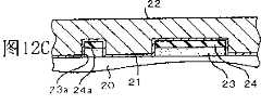
在图1中,参考标号20表示底层。该底层20具有一种结构,其中例如MOSFET形成在硅晶片(半导体基片)的活性区中,然后绝缘膜形成在该晶片的表面上,然后一个导电插塞被埋在该绝缘膜中。一个低电介性的绝缘膜23(膜厚:大约为250纳米)以及氧化硅膜24(膜厚:大约为250纳米)被叠加在该底层20上。第一绝缘膜95由低电介性绝缘膜23和氧化硅膜24所构成。In FIG. 1,
在本说明书中,低电介性绝缘膜被定义为电介常数比氧化硅膜的电介常数(4.1)更低的绝缘膜。对于这种绝缘膜,例如存在有由聚芳醚材料制成的绝缘膜。作为由聚芳醚材料所制成的绝缘膜,有SiLK(DowCorning公司的注册商标)。由于这种SiLK具有低电介常数,因此可以减小布线间电容,因此可以增加半导体器件的工作速度。In this specification, a low-dielectric insulating film is defined as an insulating film having a dielectric constant lower than that of a silicon oxide film (4.1). As such an insulating film, for example, there is an insulating film made of a polyarylene ether material. As an insulating film made of a polyarylether material, there is SiLK (registered trademark of Dow Corning Corporation). Since this SiLK has a low dielectric constant, inter-wiring capacitance can be reduced, and thus the operating speed of semiconductor devices can be increased.
开孔23a、24a被分别形成在低电介性的绝缘膜23和氧化硅膜24中。阻挡金属层21(膜厚:大约50纳米)被形成在开孔23a、24a的内壁上。这种阻挡金属层21由例如Ta(钽)等等这样的难熔金属所制成。The
参考标号22表示形成在阻挡金属层21上的铜膜。第一布线36由这种铜膜22和阻挡金属层21所构成。阻挡金属层21防止包含在铜膜22中的铜扩散到低电介性的绝缘膜23和氧化硅膜24。
为了形成这种第一布线36,首先分别在开孔23a、24a的内壁上形成阻挡金属层21,然后在其上形成铜膜22。然后,阻挡金属层21和铜膜22被通过CMP(化学机械抛光)方法而抛光和除去,从而可以获得上述结构。由于采用CMP,因此第一布线36和第一绝缘膜95的每个表面被制成足够平整。In order to form such
然后,在第一布线36和第一绝缘膜95被连续的基本上平坦的表面上形成第二绝缘膜29。第一布线36被覆盖有第二绝缘膜29。第二绝缘膜29通过重叠下绝缘膜38和上绝缘膜28而构成。这些绝缘膜38、28通过重叠各种绝缘膜而构成。例如,下绝缘膜38通过重叠氮化硅膜37(膜厚:大约50纳米)和氧化硅膜25(膜厚:大约700纳米)而构成。然后,通过重叠低电介性绝缘膜26(膜厚:大约250纳米)和氧化硅膜27(膜厚:大约250纳米)。在这些薄膜中,低电介性绝缘膜26由与低电介性的绝缘膜23相同的材料所制成,例如SiLK。Then, the second insulating
参考标号28a表示布线沟槽。该布线沟槽28a由分别形成在低电介性绝缘膜26和氧化硅膜27中的开孔26b、27b所构成。从布线沟槽28a延伸到第一布线的通孔(连接孔)38a和从布线沟槽28a延伸到不形成第一布线36的区域的伪通孔(伪连接孔)38b形成在下绝缘膜38中。通孔38a和伪通孔38b由分别形成在氮化硅膜37和氧化硅膜25中的开孔37a、25a所构成。
参考标号30表示形成在通孔38a和伪通孔38b的内壁上的阻挡金属层(膜厚:大约50纳米),并且由例如Ta(钽)这样的难熔金属所制成。该阻挡金属层30还形成在从通孔38a的底部暴露的第一布线36上。铜膜31通过阻挡金属层30被埋在通孔38a、伪通孔38b和布线沟槽28a中。
参考标号39表示被埋在布线沟槽28a中的第一布线,并且具有阻挡金属层30和铜膜31的双层结构。氮化硅膜63形成在第二布线39上。
第二布线39还被埋在通孔38a和伪通孔38b中。被埋在通孔38a中的第二布线39的部分作为导电插塞32(在下文中被称为“插塞”)。被埋在伪通孔38b中的第二布线39的部分作为伪导电插塞34(在下文中被称为“伪插塞”)。The
插塞(包括插塞32和伪插塞34)之间的位置关系在下文中讨论。在这种情况中,应当指出该位置关系可以用通孔(包括通孔38a和伪通孔38b)之间的位置关系来代替。The positional relationship between plugs (including
如下文中所述,该半导体器件通过双重镶嵌处理而制造。因此,第二布线39与插塞32和伪插塞34整体地形成。该特征没有出现在把阻挡金属层插入在布线和插塞之间的单层和双层镶嵌处理中。As described hereinafter, the semiconductor device is fabricated by a dual damascene process. Therefore, the
插塞32还被电连接到第一布线36,并且用于把第一布线36电连接到第二布线39。The
另一方面,伪插塞34构成本发明的一个特征。在图1中,L表示每对相邻插塞32、32的中央之间的距离。当没有伪插塞34时,该L为第二布线39的布线长度。On the other hand, the
但是,如本发明中所述,在提供伪通孔38b并且伪插塞34被埋在该伪通孔中的情况下,相邻插塞(包括插塞32和伪插塞34)之间的距离可以为L1或L2,并且变为比上述L更短。相应地,在本发明中,可以抑制当布线长度较长时容易出现的应力迁移,从而可以避免插塞32和第一布线36之间的接触不良。结果,由于可以降低在热处理中半导体器件的废品率,因此相应地增加半导体器件的成品率,从而可以减小半导体器件的制造成本。However, as described in the present invention, in the case where the dummy via
并且,由于在提供有伪插塞34的部分中,第二布线39的截面面积增加,因此可以减小布线电阻。相应地,还可以增加半导体器件的工作速度。Also, since the cross-sectional area of the
另外,由于该伪插塞34还作为与电子一同在第二布线39中运动的铜原子的来源,因此还可以避免由于缺乏铜原子(所谓电迁移)而断开第二布线39的情况。In addition, since this dummy plug 34 also serves as a source of copper atoms moving together with electrons in the
伪通孔38b的数目不受限制。上述优点还可以通过提供任意数目的伪通孔38b而获得。The number of dummy via
在图1中,参考标号40表示具有与第一布线36的电势不同的差别电势布线。最好,伪通孔38b在该差别电势布线之外形成。这是因为,如果伪插塞34被连接到差别电势布线40,由第一布线36和该差别电势布线40之间电连接,从而该电路不能够正常工作。In FIG. 1 ,
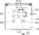
每个插塞的平面结构在图2中示出。图2为示出根据第一实施例的半导体器件的平面示图。在图2中,为了便于理解该插塞的结构,底层20(参见图1)以及每个绝缘膜被省略。并且,上述图1对应于沿着图2中的I-I线截取的截面。The planar structure of each plug is shown in FIG. 2 . FIG. 2 is a plan view showing the semiconductor device according to the first embodiment. In FIG. 2, the bottom layer 20 (see FIG. 1) and each insulating film are omitted for easy understanding of the structure of the plug. And, FIG. 1 described above corresponds to a cross section taken along line I-I in FIG. 2 .
接着,将参照图15A和15B以及图16A和16B说明本发明的发明人所作的实施例。Next, an embodiment made by the inventors of the present invention will be described with reference to FIGS. 15A and 15B and FIGS. 16A and 16B.
图15A为示出根据第一实施例的半导体器件的第一模拟结果的曲线图,以及图15B为示出用于该模拟中的模型的截面示图。图16A为示出根据第一实施例的半导体器件的第二模拟结果的曲线图,以及图16B为示出用于该模拟中的模型的截面示图。15A is a graph showing a first simulation result of the semiconductor device according to the first embodiment, and FIG. 15B is a cross-sectional view showing a model used in the simulation. 16A is a graph showing a second simulation result of the semiconductor device according to the first embodiment, and FIG. 16B is a cross-sectional view showing a model used in the simulation.
在图15A、15B、16A和16B的模拟中,相邻插塞32、32的中央之间的距离(即布线长度)被固定为10微米。然后,作为插塞32和伪插塞34的模型,采用直径为0.15微米和高度为0.42微米的圆柱体。In the simulations of FIGS. 15A, 15B, 16A, and 16B, the distance between the centers of
在第一模拟中(图15A和15B),当改变相邻伪插塞34、34之间的间距(间隔)p1时研究施加在插塞32的上表面和下表面上的应力的垂直分量的差值Δσ。如果该差值Δσ较大,则在垂直方向上施加到该插塞32的作用力变大,因此插塞32容易从第一布线36上脱离(参见图1)。换句话说,如果差值Δσ较大,则容易出现应力迁移。In the first simulation (FIGS. 15A and 15B), the vertical components of the stress exerted on the upper and lower surfaces of the
从图15A可以看出,在间距p1小于1微米的范围内该差值Δσ倾向于减小,因此不容易出现应力迁移。具体来说,如果间距p1小于0.6微米,则差值Δσ突然减小。因此,为了避免应力迁移,最好使间距p1小于1微米。并且,为了更加有效地避免应力迁移,最好使该间距p1小于0.6微米。It can be seen from FIG. 15A that the difference Δσ tends to decrease in the range where the pitch p1 is less than 1 micron, so stress migration is not easy to occur. Specifically, if the pitch p1 is smaller than 0.6 μm, the difference Δσ suddenly decreases. Therefore, in order to avoid stress migration, it is preferable to make the pitch p1 smaller than 1 micron. Furthermore, in order to avoid stress migration more effectively, it is preferable to make the pitch p1 smaller than 0.6 microns.
并且,在第二模拟中(图16A和16B),当改变第一间距p1时,研究上述差值Δσ与第一间距p1(被相邻设置的插塞32和伪插塞34之间的间距)的相关性。在这种情况中,相邻伪插塞34、34之间的距离被固定为0.3微米。And, in the second simulation (FIGS. 16A and 16B), when the first pitchp1 was changed, the relationship between the above-mentioned difference Δσ and the first pitchp1 (between the adjacently disposed
从图16A可以看出,在间距p1小于1微米的范围内该差值Δσ倾向于减小,因此不容易出现应力迁移。具体来说,如果间距p1小于0.6微米,则差值Δσ突然减小。因此,为了避免应力迁移,最好使间距p1小于1微米。并且,为了更加有效地避免应力迁移,最好使该间距p1小于0.6微米。It can be seen from FIG. 16A that the difference Δσ tends to decrease in the range where the pitch p1 is less than 1 micron, so stress migration is not easy to occur. Specifically, if the pitch p1 is smaller than 0.6 μm, the difference Δσ suddenly decreases. Therefore, in order to avoid stress migration, it is preferable to make the pitch p1 smaller than 1 micron. Furthermore, in order to avoid stress migration more effectively, it is preferable to make the pitch p1 smaller than 0.6 microns.
(2)第二实施例(2) The second embodiment
图3为示出根据本发明第二实施例的半导体器件的截面示图。在图3中,与图1相同的参考标号表示在图1中所示的相同部件,并且省略对它们的描述。3 is a cross-sectional view showing a semiconductor device according to a second embodiment of the present invention. In FIG. 3, the same reference numerals as in FIG. 1 denote the same components shown in FIG. 1, and their descriptions are omitted.
在第二实施例中,如图3中所示,伪布线41被提供在不形成第一布线36的区域中,并且形成伪通孔38b,以到达该伪布线41。然后,形成伪插塞34,以连接到该伪布线41。在这种情况中,不形成布线的区域被定义为在形成有布线的层面中没有形成布线的区域。与第一布线36相同,该伪布线41具有阻挡金属层21和铜膜22的双层结构。In the second embodiment, as shown in FIG. 3 , a
根据该描述,由于第二布线39可以由使用伪布线41作为基础的伪插塞34牢固地支承,因此由第二绝缘膜29和第二布线39所构成的叠层体的机械强度得到增强。这种优点对于用SiLK等等这样的低电介性绝缘膜取代氧化硅膜25来降低第二绝缘膜29的整体电介常数的情况特别有用。如果本实施例被应用于这种情况,则可以避免由于低电介性绝缘膜的机械强度较弱所造成的由低电介性绝缘膜和第二布线39所构成的叠层体的强度下降。According to the description, since the
在本实施例中每个插塞的平面结构在图4中示出。图4为示出根据第二实施例的半导体器件的平面示图。在图4中,为了便于理解每个插塞的结构,省略底层20(参见图3)和每个绝缘膜。并且,图3上对应于延着图4的II-II线截取的截面示图。The planar structure of each plug in this embodiment is shown in FIG. 4 . FIG. 4 is a plan view showing a semiconductor device according to a second embodiment. In FIG. 4, the bottom layer 20 (see FIG. 3) and each insulating film are omitted for easy understanding of the structure of each plug. And, FIG. 3 corresponds to a cross-sectional view taken along line II-II of FIG. 4 .
(3)第三实施例(3) The third embodiment
图5A至5C为示出根据本发明第三实施例的半导体器件的平面示图。在这些图中,为了使每个插塞的平面结构和第二布线39的平面形状容易被看到,省略底层20(参见图1和3)以及每个绝缘膜。5A to 5C are plan views showing a semiconductor device according to a third embodiment of the present invention. In these figures, in order to make the planar structure of each plug and the planar shape of the
在第一和第二实施例中,如图2和图4中所示,第二布线39的平面形状为线状。但是,第二布线39的平面形状不限于线状。该平面形状可以为立方体(solid)形状,如图5A至5C所示。In the first and second embodiments, as shown in FIGS. 2 and 4 , the planar shape of the
图5A示出一个例子,其中插塞32被提供在立方体的第二布线39的中央附近,以及多个伪插塞34被提供在这种插塞32周围。FIG. 5A shows an example in which a
图5B示出一个例子,其中插塞32被提供到立方体的第二布线39的一个边缘部分,并且多个伪插塞34被提供在每个边缘部分的附近。FIG. 5B shows an example in which a
图5C示出一个例子,其中插塞32被提供到立方体的第二布线39的一角,并且多个伪插塞34被提供在这样的一个角的附近。FIG. 5C shows an example in which a
图5A至5C中所示的所有例如可以获得与第一实施例相类似的优点。All of those shown in FIGS. 5A to 5C , for example, can obtain advantages similar to those of the first embodiment.
接着,将参照图17A至17C以及图18说明由本发明的发明人所给出的实施例。Next, an embodiment given by the inventors of the present invention will be described with reference to FIGS. 17A to 17C and FIG. 18 .
图17A至17C为示出用于该半导体器件的模拟中的模型。17A to 17C are diagrams showing models used in simulations of this semiconductor device.
图17A示出插塞32被单独提供在该立方体的第二布线39中而没有提供伪插塞34的情况。FIG. 17A shows a case where the
图17B示出伪插塞34被提供在第二布线39中以单层地包围该插塞32的情况。FIG. 17B shows a case where a
图17C示出伪插塞34被提供在第二布线39中以双层地包围该插塞32的情况。FIG. 17C shows a case where a
在图17A至17C中的所有情况中,直径为0.15微米以及高度为0.42微米的圆柱体被用作为插塞32和伪插塞34的模型。并且第二布线39的高度被固定为2微米。然后,相邻插塞(包括插塞32和伪插塞34)之间的间距被固定为0.3微米。In all cases in FIGS. 17A to 17C , a cylinder with a diameter of 0.15 microns and a height of 0.42 microns was used as a model for the
模拟结果在图18中示出。在图18中,在纵坐标上Δσ的含义类似于图15A和15B中所示的含义,并且为在插塞32和上表面和下表面上的应力的垂直分量之差。The simulation results are shown in FIG. 18 . In FIG. 18, the meaning of Δσ on the ordinate is similar to that shown in FIGS. 15A and 15B, and is the difference between the vertical components of the stress on the
从图18可以看出,插塞32被单独提供(参见图17A),并且差值Δσ较大,因此容易出现应力迁移。相反,应当知道在提供插塞34以单层或双层地包围插塞32(参见图17B和图17C)的位置,与单独地提供插塞32的情况相比,差值Δσ被减小,因此不容易出现应力迁移。As can be seen from FIG. 18 , the
结果,即使在不限定第二布线39的布线长度的情况中,类似于仅仅在立方体的第二布线39中提供一个插塞32的情况,可以通过在插塞32周围提供多个伪插塞34而减小应力迁移。换句话说,这意味着,如果在通孔38a周围提供多个伪通孔38b,则可以减小应力迁移。As a result, even in the case where the wiring length of the
(4)第四实施例(4) The fourth embodiment
图6为示出根据本发明第四实施例的半导体器件的平面示图。在图6中,为了使每个插塞和第二布线39的平面结构容易被看到,省略底层20(参见图1和3)以及每个绝缘膜。并且,图7为沿着图6中的III-III线截取的截面示图。如下文中所述,本发明适用于增加半导体器件的工作速度。FIG. 6 is a plan view showing a semiconductor device according to a fourth embodiment of the present invention. In FIG. 6, in order to make the planar structure of each plug and the
如图6中所示,在本实施例中,多个第二布线39被以某一间隔设置在一个区域A中。然后,在两个相邻的第二布线39中,在一条第二布线39中的伪插塞34不被设置在沿着与第二布线39的延伸方向相垂直的方向上与另一条第二布线中的伪插塞34相邻。在此,第二布线39的延伸方向意味着两条相邻第二布线的任意一个的延伸方向。As shown in FIG. 6 , in the present embodiment, a plurality of
由此,由于在相邻第二布线39中的伪插塞34不被设置为相对,则可以减小在伪插塞34之间的相对电容。因此,可以避免由于相对电容而造成第二布线39之间的布线间电容的增加。Thereby, since the dummy plugs 34 in adjacent
在上文中,伪插塞34之间的相对电容被考虑。但是,上文所述内容可以用于插塞32,在相邻的第二布线39中的插塞32之间的相对电容还可以被减小。另外,如果上述内容被应用于不同类型的插塞(插塞32和伪插塞34),则插塞32和伪插塞34之间的相对电容也可以被减小。In the above, the relative capacitance between the dummy plugs 34 is considered. However, the above-mentioned content can be applied to the
插塞32和伪插塞34的数目不受限制。如果上述内容应用于在第二布线39中的一部分插塞32和一部分伪插塞34,则还可以减小第二布线39之间的布线间电容。The number of
(5)第五实施例(5) fifth embodiment
图8为示出根据本发明第五实施例的半导体器件的截面示图。在图8中,与上文所述相类似的参考标号表示在上文已经描述的部件,因此将省略对它们的描述。8 is a cross-sectional view showing a semiconductor device according to a fifth embodiment of the present invention. In FIG. 8 , reference numerals similar to those described above denote components that have already been described above, and thus their descriptions will be omitted.
在第一至第四实施例中,布线具有第一布线36和第二布线39的两个层面。但是,布线层的数目不限于两层。在本实施例中,如图8中所示,第三布线51被提供在第二布线39上方,并且布线层的数目为三层。In the first to fourth embodiments, the wiring has two layers of the
该第三布线51具有由铜膜71和阻挡金属层72所构成的双层结构,并且被埋在布线沟槽69a中。布线沟槽69a被形成在上绝缘膜69中。该上绝缘膜69包括低电介性绝缘膜65(膜厚:大约250纳米)以及氧化硅膜66(膜厚:大约250纳米)。作为低电介性绝缘膜65,在上文已经描述可以采用例如SiLK这样的与低电介性绝缘膜23、26相类似的材料。上述布线沟槽69a包括形成在低电介性绝缘膜65和氧化硅膜66中的开孔65b、66b。The
在图8中,参考标号68表示由氮化硅膜63(膜厚:大约50纳米)和氧化硅膜64(膜厚:大约700纳米)所构成的下层绝缘膜。In FIG. 8,
参考标号68a表示通孔(连接孔)并且形成在下层绝缘膜68中,以到达第二布线39。该通孔68a由形成在氮化硅膜63和氧化硅膜64中的开孔63a、64a所构成。
参考标号68b表示伪通孔(伪连接孔),并且形成在下层绝缘膜68中,以到达不形成第二布线39的区域。该伪通孔68b由形成在氮化硅膜63和氧化硅膜64中的开孔63b、64b所构成。
第三布线51还被埋在通孔68a和伪通孔68b中。在下文中,被埋在通孔68a中的第三布线51的部分被称为插塞53,以及被埋在伪通孔68b中的第三布线51的部分被称为伪插塞52。The
第三绝缘膜70由下层绝缘膜68和上层绝缘膜69所构成。在此,参考标号73表示覆盖第三布线51的氮化硅膜。The third
图9为示出根据本发明第五实施例的半导体器件的平面示图。FIG. 9 is a plan view showing a semiconductor device according to a fifth embodiment of the present invention.
第三布线51的平面形状不受限制。第三布线51可以形成为线状,或者可以形成为图9中所示的立方体形状。The planar shape of the
在图9中,参考标号60表示具有与第二布线39和第三布线51不同的电势的差别电势布线,并且被形成在与第二布线39相同的层面中。最好,在第三布线51中的伪插塞52应当被形成在该差别电势布线60之外。这是因为,如果伪插塞52被连接到该差别电势布线60,则第二布线39和差别电势布线60被电连接,因此不能够正常工作。In FIG. 9 ,
然后,参考标号61表示形成在与第二布线39相同层面中的一条伪布线。伪插塞52可以连接到该伪布线61。如果它们被按照这种方式来连接,则根据与第二实施例相同的原因,由氧化硅膜64(参见图8)和第三布线51所构成的叠层体的机械强度可以得到增强。Then,
图10为示出根据本发明第五实施例的另一个半导体器件的平面示图。图11为沿着图10的IV-IV线截取的截面示图。FIG. 10 is a plan view showing another semiconductor device according to a fifth embodiment of the present invention. FIG. 11 is a cross-sectional view taken along line IV-IV of FIG. 10 .
在第四实施例中,描述了在相同层面中的布线间电容(即,第二布线39之间的电容)的减小。最好不但在相同层面中减小该布线间电容,而且还在不同层面中减小该布线间电容。In the fourth embodiment, reduction of inter-wiring capacitance (ie, capacitance between second wirings 39 ) in the same layer is described. It is preferable to reduce the inter-wiring capacitance not only in the same layer but also in different layers.
在第五实施例中,为了减小不同层面之间的布线间电容,每个插塞被设置为如图10中所示。根据这种结构,如果从第三布线51的上侧来看,在第二布线39中的伪插塞34和在第三布线51中的伪插塞52不在与第二布线39的延伸方向相垂直的方向上相邻设置。当考虑第三布线51的延伸方向而不是考虑第二布线39的延伸方向时,得到相同的结论。In the fifth embodiment, in order to reduce the inter-wiring capacitance between different levels, each plug is provided as shown in FIG. 10 . According to this structure, if viewed from the upper side of the
由此,由于在第二布线39中的伪插塞34被设置为与第三布线51中的伪插塞52相邻,则可以减小伪插塞34、52之间的相对电容。因此,可以避免由于插塞的相对电容所导致的第二布线39和第三布线51之间的布线间电容增加。Thus, since the dummy plug 34 in the
在上文中,伪插塞34、52之间的相对电容被讨论。但是,通过把上述内容应用于插塞32、53,可以减小插塞52、53之间的相对电容。另外,通过把上述内容应用于不同类型的插塞(插塞32和伪插塞52,或者插塞53和伪插塞34),还可以减小这些插塞之间的相对电容。In the above, the relative capacitance between the dummy plugs 34, 52 was discussed. However, by applying the above to the
作为用于获得上述优点的对象,插塞52、53以及伪插塞34、52的数目不受限制。如果上述内容被应用于在第二布线39和第三布线51中的一部分插塞32、51或者一部分伪插塞34、52,则还可以减小第二布线39和第三布线51之间的布线间电容。The number of
(6)制造方法的描述(6) Description of manufacturing method
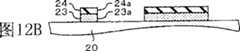
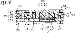
接着,在下文中将参照图12A至12N描述上述半导体器件的制造方法。图12A至12N为示出制造根据本发明的实施例的半导体器件的方法的截面示图。该制造方法也被称为双重镶嵌处理,其中整体形成该布线和插塞。Next, a method of manufacturing the above-described semiconductor device will be described hereinafter with reference to FIGS. 12A to 12N . 12A to 12N are cross-sectional views illustrating a method of manufacturing a semiconductor device according to an embodiment of the present invention. This manufacturing method is also called a dual damascene process, in which the wiring and the plug are integrally formed.
首先,如图12A中所示,在底层20上形成低电介性的绝缘膜23(膜厚:大约250纳米)。该底层20具有一种结构,例如其中MOSFET被形成在硅晶片(半导体基片)的活性区,然后在该晶片的表面上形成绝缘膜,然后把导电插塞埋在该绝缘膜中。First, as shown in FIG. 12A, a low-dielectric insulating film 23 (film thickness: about 250 nm) is formed on the
SiLK可以被用作为低电介性的绝缘膜23。SiLK被通过旋涂方法施加,并且通过在400℃的温度下执行30分钟的退火处理而固化。SiLK can be used as the low-dielectric insulating
然后,氧化硅膜24(膜厚:大约250纳米)被形成在低电介性的绝缘膜23上。为了形成氧化硅膜24,例如采用公知的等离子体增强CVD(等离子体增强化学汽相淀积)方法。Then, a silicon oxide film 24 (film thickness: approximately 250 nm) is formed on the low-dielectric insulating
然后,光刻胶层54被形成在氧化硅膜24上。分别具有布线图案形状的开孔54a被通过光刻形成在光刻胶层54中。Then, a photoresist layer 54 is formed on the
然后,如图12B中所示,通过使用光刻胶层54作为掩膜蚀刻氧化硅膜24。该开孔54a被通过蚀刻而转印到氧化硅膜24上,从而在氧化硅膜24中形成开孔24a。并且,该蚀刻通过使用RIE(反应离子蚀刻)和CF腐蚀气而执行。Then, as shown in FIG. 12B, the
然后,通过使用氧化硅膜24作为蚀刻掩膜,蚀刻低电介性的绝缘膜23。开孔24a被通过该蚀刻而转印到低电介性的绝缘膜23,从而在低电介性的绝缘膜23中形成开孔23a。作为用于该蚀刻中的腐蚀气,采用包括H2和NH3的等离子化气体混合物。对于该腐蚀气,光刻胶层54具有基本上与低电介性的绝缘膜23相同的蚀刻率。因此,当低电介性的绝缘膜23被蚀刻时,光刻胶层54被同时除去。Then, the low-dielectric insulating
然后,如图12C中所示,阻挡金属层21(膜厚:大约50纳米)被形成在整个暴露表面上。这种阻挡金属层21由例如Ta等等这样的难熔金属所制成,并且通过溅射等方法所形成。Then, as shown in FIG. 12C, a barrier metal layer 21 (film thickness: about 50 nm) is formed on the entire exposed surface. This
然后,铜膜22被形成在阻挡金属层21上。通过溅射而形成铜膜22,并且具有可以完全填充开孔23a、24a的膜厚。形成铜膜22的方法不受限制。作为上述方法的一种代替方法,单个铜种子层可以形成在阻挡金属层21上,然后,可以通过使用该钟子层作为电源层,通过电镀而形成铜膜22。Then, a
然后,如图12D中所示,随着在铜膜22的表面上的电镀一同,通过CMP(化学机械抛光)方法而除去在氧化硅膜24上的不需要的铜膜22和不需要的阻挡金属层21。因此仅仅在开孔23a、24a中保留铜膜22和阻挡金属层21。剩余的铜膜22和阻挡金属层21构成第一布线36和伪布线41。可以通过CMP方法在连续的第一布线36和第一绝缘膜95的表面上获得基本上平整的表面。Then, as shown in FIG. 12D, along with the electroplating on the surface of the
通过这种方法,为了良好执行上述CMP方法,最好在该平面中包括第一布线36和伪布线41的总布线占有率基本上为常量。在本说明书中,“布线占有率”被定义为通过在布线层中设置任意面积A的虚拟区域(其形状不受限制)然后由面积A除在该虚拟区域中的布线的总面积B而得的数值(B/A)。By this method, in order to perform well the above-mentioned CMP method, it is preferable that the total wiring occupancy ratio including the
如果布线密度如图13中所示极大地变化,由于该比率在密集布线部分和稀疏布线部分之间具有较大的差别,则不能够认为该布线占有率为常量。在这种情况中,由于CMP膏剂分散到密集布线部分的第一布线36和伪布线41中,则抛光量变小,因此在密集部分中的被抛光布线的高度变高。相反,由于CMP膏剂集中到在稀疏布线部分中的第一布线36,因此抛光量变大,从而在稀疏部分中被抛光的布线的高度变低。If the wiring density varies greatly as shown in FIG. 13, since the ratio has a large difference between the densely wired part and the sparsely wired part, the wiring occupancy cannot be considered constant. In this case, since the CMP paste is dispersed into the
按照这种方式,当在该平面中的布线占有率不为常量时,导致在布线的高度中的变化,因此难以控制布线的高度。In this way, when the wiring occupancy in the plane is not constant, variation in the height of the wiring is caused, and thus it is difficult to control the height of the wiring.
相反,如图12D中所示,如果布线占有率基本上为常量,则CMP膏剂被均匀地分散到第一布线36和伪布线41。因此,在平面中的抛光量不变,从而布线高度可以被容易地控制。In contrast, as shown in FIG. 12D , if the wiring occupancy is substantially constant, the CMP paste is uniformly dispersed to the
在如上文所述执行CMP之后,执行图12E中所示的步骤。在这些步骤中,氮化硅膜37(膜厚:大约50纳米)被形成以覆盖第一布线36和伪布线41。该氮化硅膜37例如通过公知的等离子体增强CVD方法而形成。After performing CMP as described above, the steps shown in FIG. 12E are performed. In these steps, a silicon nitride film 37 (film thickness: approximately 50 nm) is formed to cover the
然后,氧化硅膜25(膜厚:大约1200纳米)被形成在氮化硅膜37上。氧化硅膜25也通过公知的等离子体增强CVD方法所形成,然后通过CMP方法对氧化硅膜25的表面进行平面化。通过该CMP方法使得氧化硅膜25的剩余厚度变为大约700纳米。通过氮化硅膜37和剩余的氧化硅膜25而构成下绝缘膜38。Then, a silicon oxide film 25 (film thickness: approximately 1200 nm) is formed on the
然后,低电介性绝缘膜26(膜厚:大约250纳米)、氧化硅膜27(膜厚:大约250纳米)以及氧化硅膜25被叠加在氧化硅膜25上。上绝缘膜28由低电介性绝缘膜26和氧化硅膜27所构成。Then, a low-dielectric insulating film 26 (film thickness: about 250 nm), a silicon oxide film 27 (film thickness: about 250 nm), and a
作为低电介性绝缘膜26,可以采用SiLK等材料。并且,通过公知的等离子体增强CVD方法形成氧化硅膜27。氧化硅膜25例如由TiN所形成,并且通过溅射等方法而形成。例如氮化硅膜这样具有对氧化硅膜高度选择性蚀刻率的薄膜可以被用于取代金属膜55。A material such as SiLK can be used as the low-dielectric insulating
然后,在形成金属膜55之后,在其上形成光刻胶层56。通过光刻方法在光刻胶层56中形成具有布线图案形状的开孔56a。Then, after the
然后,如图12F中所示,通过使用光刻胶层56作为蚀刻掩膜而蚀刻金属膜55。因此,开孔56a被转印到金属膜55上,从而在金属膜55中形成开孔55a。通过RIE而执行蚀刻,并且采用包含Cl的腐蚀气。在完成蚀刻之后,通过使用O2等离子体执行灰化处理而除去光刻胶层56。Then, as shown in FIG. 12F, the
然后,如图12G中所示,形成一个新的光刻胶层57。光刻胶层57的形成区域在金属膜55和从开孔55a暴露的氧化硅膜27上。通过光刻方法,在光刻胶层57中形成具有通孔图案形状的开孔57a。Then, as shown in FIG. 12G, a new photoresist layer 57 is formed. The photoresist layer 57 is formed on the
然后,如图12H中所示,通过使用光刻胶层57作为蚀刻掩膜而蚀刻氧化硅膜27。这种蚀刻通过RIE方法而执行,并且采用包含CF的腐蚀气。由于低电介性绝缘膜26具有抵抗该腐蚀气的抗腐蚀性,因此该蚀刻止于低电介性绝缘膜26的表面。因此,在光刻胶层57中的通孔57a被通过该蚀刻而转印到氧化硅膜27,因此在氧化硅膜27中形成开孔27a。Then, as shown in FIG. 12H , the
然后,如图12I中所示,通过使用氧化硅膜27作为蚀刻掩膜而蚀刻低电介性绝缘膜26。因此,开孔27a被转印到低电介性绝缘膜26,从而开孔26a被形成在低电介性绝缘膜26中。使用包含H2和NH3的气体混合物作为腐蚀气通过RIE方法而执行蚀刻。Then, as shown in FIG. 12I, the low-dielectric insulating
对于该腐蚀气,光刻胶层57(参见图12H)具有基本上与低电介性绝缘膜26相同的蚀刻率。因此,当低电介性绝缘膜26被蚀刻时,光刻胶层57被除去。With this etching gas, the photoresist layer 57 (see FIG. 12H ) has substantially the same etching rate as the low-dielectric insulating
然后,如图12J中所示,通过使用金属膜55作为蚀刻掩膜而蚀刻氧化硅膜27。因此,开孔55a被转印到氧化硅膜27,因此开孔27b被形成在氧化硅膜27中。使用包含CF的腐蚀气通过RIE执行蚀刻。Then, as shown in FIG. 12J , the
在此时,在低电介性绝缘膜26中,从开孔26a暴露出来的氧化硅膜25被同时蚀刻。因此,开孔26a被转印到氧化硅膜25上,并且在氧化硅膜25中形成开孔25a。At this time, in the low-dielectric insulating
然后,如图12K中所示,通过使用氧化硅膜27作为蚀刻掩膜而蚀刻低电介性绝缘膜26。因此,在氧化硅膜27中的开孔27b被转印到低电介性绝缘膜26上,并且在低电介性绝缘膜26中形成开孔26b。使用包含H2和NH3的气体混合物作为腐蚀气通过RIE方法而执行蚀刻。Then, as shown in FIG. 12K, the low-dielectric insulating
然后,通过使用氧化硅膜25作为蚀刻掩膜而蚀刻氮化硅膜37。在氧化硅膜25中的开孔25a被转印到氮化硅膜37上,并且在氮化硅膜37中形成开孔37a。Then, the
在这种情况中,可以先后蚀刻低电介性绝缘膜26和氮化硅膜37中的任意一个。In this case, either one of the low-dielectric insulating
到该步骤为止,完成通孔38a、伪通孔38b和布线沟槽28a的形成。通过开孔27b和26b而构成布线沟槽28a。并且,分别由开孔25a和37a构成通孔38a和伪通孔38b。Up to this step, the formation of the via
该通孔38a被形成为从布线沟槽28a延伸到第一布线36。然后,伪通孔38b可以被形成为到达不形成第一布线36的区域,或者到达伪布线41。The via
然后,如图12L中所示,形成阻挡金属层30。阻挡金属层30的形成区域在金属膜55上、布线沟槽28a的内壁上、通孔38a的内壁(包括底部表面)上以及伪通孔38b的内壁(包括底部表面)上。阻挡金属层30由例如Ta(钽)这样的难熔金属所制成,并且通过溅射等方法而形成。Then, as shown in FIG. 12L ,
然后,通过溅射方法在阻挡金属层30上形成铜膜31(膜厚:大约1500纳米)。形成铜膜31的方法不限于此。例如可以在阻挡金属层30上形成薄的铜种子层,然后使用该种子层作为电源层通过电镀形成铜膜31。Then, a copper film 31 (film thickness: approximately 1500 nm) was formed on the
然后,如图12M中所示,分别被形成为比氧化硅膜27更高的阻挡金属层30和金属膜55被通过CMP方法而抛光并除去。不被抛光并且留下的阻挡金属层30和铜膜31构成第二布线39。然后,被埋在通孔38a中的第二布线39的部分作为该插塞,并且被埋在伪通孔38b中的第二布线39的部分作为伪插塞。并且,可以通过该CMP方法而在被连接的第二布线39和第二绝缘膜29的表面上获得基本上平坦的表面。Then, as shown in FIG. 12M, the
然后,如图12N所示,氮化硅膜63被形成在第二布线39上。该氮化硅膜63由公知的等离子体增强CVD方法所形成。Then, as shown in FIG. 12N , a
根据上文所述,完成根据本发明的实施例的半导体器件。From the above, the semiconductor device according to the embodiment of the present invention is completed.
尽管在上文中获得两个布线层(第一布线36和第二布线39)的结构,但是通过重复上文所述的方法可以叠加任何数目的布线。下面将说明层叠4个层面的情况。Although the structure of two wiring layers (
图14为示出层叠4个布线层的情况的截面示图。在本例中,在硅基片96的预定区域中形成器件隔离沟槽。然后,例如氧化硅这样的绝缘体被埋在器件隔离沟槽中,从而形成浅沟槽隔离(STI)的器件隔离绝缘区80。FIG. 14 is a cross-sectional view showing a case where four wiring layers are laminated. In this example, device isolation trenches are formed in predetermined regions of the
然后,在由器件隔离绝缘区80所确定的阱81的活性区上形成栅极84和侧壁衬垫83,然后通过在栅极84的两侧上进行离子注入而形成源/漏区S/D。阻蚀膜82被形成为覆盖绝缘栅极84,然后在其上形成层间绝缘膜87。形成由阻挡金属层85和金属膜86所构成的导电插塞,以通过层间绝缘膜87和阻蚀膜82。在本实施例和本发明的每个实施例中的底层20例如由上述部件所构成。Then, a gate 84 and a sidewall liner 83 are formed on the active region of the well 81 defined by the device
然后,第一绝缘膜95被通过上述方法而形成在层间绝缘膜87上,然后第一布线36被埋在第一绝缘膜95中。Then, the first insulating
然后,通过上述方法把第二绝缘膜29形成在第一布线36上,并且第二布线39被埋在第二绝缘膜29中。如上文所述,在埋住第二布线39之后可以在连续的第二布线39和第二绝缘膜29的表面上获得基本上平整的表面。Then, the second insulating
氮化硅膜63和氧化硅膜64被形成在第二布线39上。然后,通过CMP方法对氧化硅膜64的表面抛光以进行平面化。A
然后,在氧化硅膜64上形成低电介性绝缘膜65和氧化硅膜66。例如可以采用SiLK作为低电介性绝缘膜65。通过公知的等离子体增强CVD方法形成氧化硅膜66。该氮化硅膜63、氧化硅膜64、低电介性绝缘膜65和氧化硅膜66构成第三绝缘膜70。Then, a low-dielectric insulating
接着,通过类似于上文所述用来在第二绝缘膜29中埋住第二布线39的方法,在第三绝缘膜70中埋住第三布线51。由于在埋住第二布线39之后执行CMP方法,因此可以在连续的第三布线51和第三绝缘膜70上获得基本上平整的表面。Next, the
然后,氮化硅膜73和氧化硅膜88被层叠在第三绝缘膜70上。通过公知的等离子体增强CVD方法形成这些薄膜。然后通过执行CMP方法对氧化硅膜88的表面进行抛光,以进行平面化。下绝缘膜97由氮化硅膜73和氧化硅膜88所构成。Then, the
接着,低电介性绝缘膜89和氧化硅膜90被叠加在下绝缘膜97上。可以采用SiLK等材料作为该低电介性绝缘膜89。然后,通过公知的等离子体增强CVD方法形成氧化硅膜90。上绝缘膜98由低电介性绝缘膜89和氧化硅膜90所构成。并且,第四绝缘膜99由上绝缘膜98和下绝缘膜97所构成。Next, a low-dielectric insulating
然后,通过类似于上文所述用于把第二布线39埋在第二绝缘膜29中的方法,把第四布线埋在第四绝缘膜99中。这种第四布线94具有由阻挡金属层92和铜膜93所构成的双层结构,并且阻挡金属层92由例如Ta(钽)这样的难熔金属所制成。由于在埋住第四布线94之后执行CMP方法,因此,可以在连续的第四布线94和第四绝缘膜99的表面上获得基本上平整的表面。最后,氮化硅膜91形成在第四布线94上,以保护该第四布线94。Then, the fourth wiring is buried in the fourth insulating film 99 by a method similar to that described above for burying the
尽管在上文中已经描述本发明的实施例,但是本发明不限于上述实施例。Although the embodiments of the present invention have been described above, the present invention is not limited to the above-described embodiments.
例如,在上述实施例中,可以用铝膜来取代铜膜22、31、71、93。For example, in the above-described embodiments, aluminum films may be used instead of
另外,上绝缘膜28不限于由低电介性绝缘膜26和氧化硅膜27所构成的叠层结构。类似于下绝缘膜38,上绝缘膜28可以由氮化硅膜和氧化硅膜构成的叠层体所制成。In addition, the upper insulating
如上文所述,根据本发明的半导体器件,由于伪连接孔被提供在第二绝缘膜中,然后通过在该孔中埋住第二布线而形成伪导电插塞,因此可以提高抗应力迁移性。As described above, according to the semiconductor device of the present invention, since the dummy connection hole is provided in the second insulating film, and then the dummy conductive plug is formed by burying the second wiring in the hole, stress migration resistance can be improved. .
并且,由于伪布线被提供在不形成第一布线的区域并且然后通过形成到达伪布线的伪连接孔而把伪导电插塞连接到该伪布线,因此可以增强由绝缘膜和第二布线所构成的叠层体的机械强度。Also, since the dummy wiring is provided in a region where the first wiring is not formed and then the dummy conductive plug is connected to the dummy wiring by forming a dummy connection hole reaching the dummy wiring, it is possible to enhance the configuration of the insulating film and the second wiring. The mechanical strength of the laminate.
由于在平面中包括第一布线和伪布线在内的总布线占有率基本上为常量,因此可以容易地在CMP中控制伪布线和第一布线的抛光高度。Since the total wiring occupancy rate including the first wiring and the dummy wiring is substantially constant in a plane, the polishing heights of the dummy wiring and the first wiring can be easily controlled in CMP.
另外,由于相邻伪连接孔之间的间距p1被设置为小于1微米,因此可以减小应力迁移。In addition, since the pitchp1 between adjacent dummy connection holes is set to be less than 1 micron, stress migration can be reduced.
特别地,如果间距p1被设置为小于0.6微米,则可以更加有效地减小应力迁移。In particular, if the pitch p1 is set to be smaller than 0.6 μm, stress migration can be reduced more effectively.
类似地,如果相邻连接孔和伪连接孔之间的间距p1被设置为小于1微米,因此可以减小应力迁移。Similarly, if the pitch p1 between adjacent connection holes and dummy connection holes is set to be less than 1 μm, stress migration can thus be reduced.
然后,如果间距p1被设置为小于0.6微米,则可以更加有效地减小应力迁移。Then, if the pitch p1 is set to be smaller than 0.6 μm, stress migration can be reduced more effectively.
另外,由于提供多个布线使得在相邻的第二布线中的导电插塞和伪导电插塞相互不正对,则可以减小相邻的第二布线之间的布线间电容。In addition, since a plurality of wirings are provided such that the conductive plugs and dummy conductive plugs in adjacent second wirings do not face each other, the inter-wiring capacitance between adjacent second wirings can be reduced.
另外,连接到导电插塞和伪导电插塞的第三布线可以被设置在比第二布线更高的位置处。在这种情况中,如果从第三布线的上侧来看,由于第三布线被提供使得导电插塞和伪导电插塞不再第二布线和第三布线中相互正对,则可以减小第二布线和第三布线之间的布线间电容。In addition, a third wiring connected to the conductive plug and the dummy conductive plug may be provided at a higher position than the second wiring. In this case, if viewed from the upper side of the third wiring, since the third wiring is provided so that the conductive plug and the dummy conductive plug are no longer facing each other in the second wiring and the third wiring, it is possible to reduce Inter-wiring capacitance between the second wiring and the third wiring.
然后,如果包含低电介性绝缘膜的绝缘膜被用作为该绝缘膜,则可以减小布线间电容,因此可以增加半导体器件的工作速度。Then, if an insulating film including a low-dielectric insulating film is used as the insulating film, the inter-wiring capacitance can be reduced, and thus the operating speed of the semiconductor device can be increased.
Claims (16)
Applications Claiming Priority (2)
| Application Number | Priority Date | Filing Date | Title |
|---|---|---|---|
| JP390710/2001 | 2001-12-21 | ||
| JP2001390710AJP3790469B2 (en) | 2001-12-21 | 2001-12-21 | Semiconductor device |
Publications (2)
| Publication Number | Publication Date |
|---|---|
| CN1428855A CN1428855A (en) | 2003-07-09 |
| CN1231970Ctrue CN1231970C (en) | 2005-12-14 |
Family
ID=19188438
Family Applications (1)
| Application Number | Title | Priority Date | Filing Date |
|---|---|---|---|
| CNB021575487AExpired - Fee RelatedCN1231970C (en) | 2001-12-21 | 2002-12-20 | Semiconductor device |
Country Status (6)
| Country | Link |
|---|---|
| US (2) | US7067919B2 (en) |
| EP (2) | EP1326276B1 (en) |
| JP (1) | JP3790469B2 (en) |
| KR (1) | KR100847649B1 (en) |
| CN (1) | CN1231970C (en) |
| TW (1) | TW569389B (en) |
Families Citing this family (45)
| Publication number | Priority date | Publication date | Assignee | Title |
|---|---|---|---|---|
| JP4005873B2 (en) | 2002-08-15 | 2007-11-14 | 株式会社東芝 | Semiconductor device |
| JP3858849B2 (en)* | 2003-04-16 | 2006-12-20 | ソニー株式会社 | Semiconductor device and manufacturing method thereof |
| JP2004363256A (en)* | 2003-06-03 | 2004-12-24 | Nec Electronics Corp | Semiconductor device and method for manufacturing the same |
| JP2005064226A (en) | 2003-08-12 | 2005-03-10 | Renesas Technology Corp | Wiring structure |
| US20050045993A1 (en)* | 2003-08-28 | 2005-03-03 | Sanyo Electric Co., Ltd. | Semiconductor device with concave patterns in dielectric film and manufacturing method thereof |
| US7387960B2 (en)* | 2003-09-16 | 2008-06-17 | Texas Instruments Incorporated | Dual depth trench termination method for improving Cu-based interconnect integrity |
| JP2006024698A (en)* | 2004-07-07 | 2006-01-26 | Toshiba Corp | Semiconductor device and manufacturing method thereof |
| US20060180934A1 (en)* | 2005-02-14 | 2006-08-17 | Taiwan Semiconductor Manufacturing Co., Ltd. | Wiring structures for semiconductor devices |
| JP4590556B2 (en)* | 2005-03-11 | 2010-12-01 | 国立大学法人 奈良先端科学技術大学院大学 | Manufacturing method of semiconductor device |
| KR100640535B1 (en)* | 2005-05-13 | 2006-10-30 | 동부일렉트로닉스 주식회사 | Multilayer copper interconnection structure of semiconductor device having dummy via contact and method of forming the same |
| US7224069B2 (en)* | 2005-07-25 | 2007-05-29 | Taiwan Semiconductor Manufacturing Company, Ltd. | Dummy structures extending from seal ring into active circuit area of integrated circuit chip |
| DE102005057076A1 (en)* | 2005-11-30 | 2007-05-31 | Advanced Micro Devices, Inc., Sunnyvale | Increasing adhesion of metal layers comprises determination of regions of reduced contact hole density and formation of position-holding contacts with metal |
| WO2007064471A1 (en)* | 2005-11-30 | 2007-06-07 | Advanced Micro Devices, Inc. | A technique for increasing adhesion of metallization layers by providing dummy vias |
| CN1983550A (en)* | 2005-12-14 | 2007-06-20 | 中芯国际集成电路制造(上海)有限公司 | Method for improving reliability and finished-product rate and eliminating copper offset |
| TW200735274A (en)* | 2005-12-29 | 2007-09-16 | Koninkl Philips Electronics Nv | Reliability improvement of metal-interconnect structure by capping spacers |
| US7767570B2 (en)* | 2006-03-22 | 2010-08-03 | Taiwan Semiconductor Manufacturing Company, Ltd. | Dummy vias for damascene process |
| JP2007305713A (en)* | 2006-05-10 | 2007-11-22 | Matsushita Electric Ind Co Ltd | Semiconductor device and wiring auxiliary pattern generation method |
| JP5050413B2 (en) | 2006-06-09 | 2012-10-17 | 富士通株式会社 | Design support program, recording medium storing the program, design support method, and design support apparatus |
| US8912657B2 (en)* | 2006-11-08 | 2014-12-16 | Rohm Co., Ltd. | Semiconductor device |
| US7777340B2 (en)* | 2006-11-08 | 2010-08-17 | Rohm Co., Ltd. | Semiconductor device |
| JP4731456B2 (en) | 2006-12-19 | 2011-07-27 | 富士通セミコンダクター株式会社 | Semiconductor device |
| JP4871168B2 (en) | 2007-02-26 | 2012-02-08 | 富士通セミコンダクター株式会社 | Integrated circuit wiring route search method, integrated circuit automatic wiring apparatus, and program |
| US7964934B1 (en) | 2007-05-22 | 2011-06-21 | National Semiconductor Corporation | Fuse target and method of forming the fuse target in a copper process flow |
| US8030733B1 (en) | 2007-05-22 | 2011-10-04 | National Semiconductor Corporation | Copper-compatible fuse target |
| US20090079080A1 (en)* | 2007-09-24 | 2009-03-26 | Infineon Technologies Ag | Semiconductor Device with Multi-Layer Metallization |
| KR20090054544A (en)* | 2007-11-27 | 2009-06-01 | 주식회사 동부하이텍 | Metal wiring process |
| JP5251153B2 (en)* | 2008-02-07 | 2013-07-31 | 富士通セミコンダクター株式会社 | Semiconductor device |
| US8669597B2 (en) | 2008-05-06 | 2014-03-11 | Spansion Llc | Memory device interconnects and method of manufacturing |
| US7951704B2 (en)* | 2008-05-06 | 2011-05-31 | Spansion Llc | Memory device peripheral interconnects and method of manufacturing |
| JP5350681B2 (en)* | 2008-06-03 | 2013-11-27 | ルネサスエレクトロニクス株式会社 | Semiconductor device |
| JP5353109B2 (en) | 2008-08-15 | 2013-11-27 | 富士通セミコンダクター株式会社 | Manufacturing method of semiconductor device |
| US7709956B2 (en)* | 2008-09-15 | 2010-05-04 | National Semiconductor Corporation | Copper-topped interconnect structure that has thin and thick copper traces and method of forming the copper-topped interconnect structure |
| JP5434355B2 (en)* | 2009-08-11 | 2014-03-05 | 富士通セミコンダクター株式会社 | Design support program, design support apparatus, and design support method |
| DE102009056562A1 (en)* | 2009-12-03 | 2011-06-09 | Telefunken Semiconductors Gmbh & Co. Kg | Integrated circuit part |
| US20110133286A1 (en)* | 2009-12-03 | 2011-06-09 | Franz Dietz | Integrierter schaltungsteil |
| US8513114B2 (en)* | 2011-04-29 | 2013-08-20 | Renesas Electronics Corporation | Method for forming a dual damascene interconnect structure |
| KR20120138875A (en)* | 2011-06-16 | 2012-12-27 | 삼성전자주식회사 | Wiring structures and methods of manufacturing the same |
| US8941242B2 (en)* | 2011-12-07 | 2015-01-27 | Freescale Semiconductor, Inc. | Method of protecting against via failure and structure therefor |
| US9343411B2 (en)* | 2013-01-29 | 2016-05-17 | Intel Corporation | Techniques for enhancing fracture resistance of interconnects |
| US9966338B1 (en) | 2017-04-18 | 2018-05-08 | Globalfoundries Inc. | Pre-spacer self-aligned cut formation |
| KR102307127B1 (en)* | 2017-06-14 | 2021-10-05 | 삼성전자주식회사 | Semiconductor device |
| JP7085417B2 (en)* | 2018-06-25 | 2022-06-16 | ルネサスエレクトロニクス株式会社 | Semiconductor equipment |
| JP7082019B2 (en)* | 2018-09-18 | 2022-06-07 | 株式会社東芝 | Solid-state image sensor |
| US11164815B2 (en)* | 2019-09-28 | 2021-11-02 | International Business Machines Corporation | Bottom barrier free interconnects without voids |
| US12349495B2 (en)* | 2020-02-21 | 2025-07-01 | Canon Kabushiki Kaisha | Semiconductor device and method for manufacturing semiconductor device |
Family Cites Families (24)
| Publication number | Priority date | Publication date | Assignee | Title |
|---|---|---|---|---|
| EP0457449A1 (en)* | 1990-04-27 | 1991-11-21 | Fujitsu Limited | Semiconductor device having via hole and method of producing the same |
| JP3277098B2 (en)* | 1994-07-26 | 2002-04-22 | 株式会社東芝 | Method for manufacturing semiconductor device |
| JP2710221B2 (en)* | 1995-01-25 | 1998-02-10 | 日本電気株式会社 | Semiconductor device and manufacturing method thereof |
| US6245996B1 (en)* | 1996-09-27 | 2001-06-12 | Compaq Computer Corporation | Electrical interconnect structure having electromigration-inhibiting segments |
| JPH10233442A (en) | 1997-02-18 | 1998-09-02 | Sony Corp | Semiconductor device and its manufacturing method |
| JP3638778B2 (en)* | 1997-03-31 | 2005-04-13 | 株式会社ルネサステクノロジ | Semiconductor integrated circuit device and manufacturing method thereof |
| JP2926568B1 (en) | 1998-02-25 | 1999-07-28 | 九州日本電気株式会社 | Semiconductor integrated circuit and its wiring method |
| JPH11340321A (en)* | 1998-05-27 | 1999-12-10 | Sony Corp | Semiconductor device and its manufacture |
| JP2000012688A (en)* | 1998-06-24 | 2000-01-14 | Sharp Corp | Semiconductor device and manufacturing method thereof |
| JP3566583B2 (en)* | 1999-06-30 | 2004-09-15 | 株式会社東芝 | Method for manufacturing semiconductor device |
| JP2001044196A (en) | 1999-07-30 | 2001-02-16 | Fujitsu Ltd | Semiconductor device |
| JP2001077543A (en)* | 1999-09-03 | 2001-03-23 | Fujitsu Ltd | Multilayer wiring board |
| KR100356135B1 (en)* | 1999-12-08 | 2002-10-19 | 동부전자 주식회사 | Method for fabricating a semiconductor device |
| JP2001185552A (en)* | 1999-12-27 | 2001-07-06 | Hitachi Ltd | Semiconductor integrated circuit device and method of manufacturing the same |
| JP4979154B2 (en) | 2000-06-07 | 2012-07-18 | ルネサスエレクトロニクス株式会社 | Semiconductor device |
| US6432811B1 (en)* | 2000-12-20 | 2002-08-13 | Intel Corporation | Method of forming structural reinforcement of highly porous low k dielectric films by Cu diffusion barrier structures |
| US6468894B1 (en)* | 2001-03-21 | 2002-10-22 | Advanced Micro Devices, Inc. | Metal interconnection structure with dummy vias |
| JP2002289687A (en)* | 2001-03-27 | 2002-10-04 | Sony Corp | Semiconductor device and method for wiring in semiconductor device |
| US6489684B1 (en)* | 2001-05-14 | 2002-12-03 | Taiwan Semiconductor Manufacturing Company | Reduction of electromigration in dual damascene connector |
| US6717268B2 (en)* | 2001-11-13 | 2004-04-06 | Intel Corporation | Electromigration-reliability improvement of dual damascene interconnects |
| JP2004031439A (en)* | 2002-06-21 | 2004-01-29 | Renesas Technology Corp | Semiconductor integrated circuit device and method of manufacturing the same |
| JP4121356B2 (en)* | 2002-10-31 | 2008-07-23 | 富士通株式会社 | Semiconductor device |
| JP4047324B2 (en)* | 2003-12-03 | 2008-02-13 | 松下電器産業株式会社 | Semiconductor device and manufacturing method thereof |
| JP2006080333A (en)* | 2004-09-10 | 2006-03-23 | Toshiba Corp | Semiconductor device |
- 2001
- 2001-12-21JPJP2001390710Apatent/JP3790469B2/ennot_activeExpired - Lifetime
- 2002
- 2002-11-26TWTW091134354Apatent/TW569389B/ennot_activeIP Right Cessation
- 2002-12-04USUS10/309,113patent/US7067919B2/ennot_activeExpired - Lifetime
- 2002-12-05EPEP02026987.4Apatent/EP1326276B1/ennot_activeExpired - Lifetime
- 2002-12-05EPEP10177318.2Apatent/EP2264758B1/ennot_activeExpired - Lifetime
- 2002-12-20CNCNB021575487Apatent/CN1231970C/ennot_activeExpired - Fee Related
- 2002-12-20KRKR1020020081656Apatent/KR100847649B1/ennot_activeExpired - Fee Related
- 2005
- 2005-01-18USUS11/035,745patent/US7173337B2/ennot_activeExpired - Lifetime
Also Published As
| Publication number | Publication date |
|---|---|
| US20030116852A1 (en) | 2003-06-26 |
| US7067919B2 (en) | 2006-06-27 |
| EP2264758B1 (en) | 2017-03-01 |
| JP3790469B2 (en) | 2006-06-28 |
| TW569389B (en) | 2004-01-01 |
| KR20030053047A (en) | 2003-06-27 |
| CN1428855A (en) | 2003-07-09 |
| US7173337B2 (en) | 2007-02-06 |
| EP2264758A2 (en) | 2010-12-22 |
| EP1326276A3 (en) | 2005-04-06 |
| EP1326276B1 (en) | 2014-10-15 |
| US20050121788A1 (en) | 2005-06-09 |
| JP2003197623A (en) | 2003-07-11 |
| KR100847649B1 (en) | 2008-07-21 |
| EP2264758A3 (en) | 2012-01-25 |
| EP1326276A2 (en) | 2003-07-09 |
| TW200301543A (en) | 2003-07-01 |
Similar Documents
| Publication | Publication Date | Title |
|---|---|---|
| CN1231970C (en) | Semiconductor device | |
| CN1290186C (en) | Semiconductor device and method for manufacturing the same | |
| CN1309077C (en) | Semiconductor device comprising low dielectric material film and its production method | |
| CN1155072C (en) | Semiconductor device with trench isolation structure and fabrication method thereof | |
| CN1096116C (en) | Semiconductor device and manufacturing method thereof | |
| CN1205664C (en) | Semiconductor device and manufacturing method thereof | |
| CN1135618C (en) | Semiconductor device and manufacturing method thereof | |
| CN101044605A (en) | Semiconductor device and its making method | |
| CN1956173A (en) | Semiconductor device and its manufacturing method | |
| CN1800972A (en) | Semiconductor device and its manufacturing method and phase-shift mask | |
| CN1701418A (en) | Manufacturing method of semiconductor device, semiconductor wafer and semiconductor device | |
| CN1354521A (en) | Semiconductor device and manufacturing mehtod thereof | |
| CN101030557A (en) | Semiconductor device and process for producing the same | |
| CN1725511A (en) | Semiconductor device and manufacturing method thereof | |
| CN1444279A (en) | Semiconductor device and its mfg. method | |
| CN1300846C (en) | Semiconductor device and method of fabricating same | |
| CN1941368A (en) | Integrated circuit arrangement having a plurality of conductive structure levels and capacitor, and a method for producing the integrated circuit arrangement | |
| CN1601741A (en) | Semiconductor device and manufacturing method thereof | |
| CN1118095C (en) | Fabrication method of semiconductor device using CMP process | |
| CN100336199C (en) | Process for producing semiconductor device | |
| CN1893034A (en) | Semiconductor device | |
| CN1359157A (en) | Semiconductor device with capacitance component and making method | |
| CN1191630C (en) | Semiconductor device and method for manufacturing semiconductor device | |
| CN1682359A (en) | Semiconductor device and manufacturing method thereof | |
| CN1873963A (en) | Semiconductor device and method of manufacturing a semiconductor device |
Legal Events
| Date | Code | Title | Description |
|---|---|---|---|
| C06 | Publication | ||
| PB01 | Publication | ||
| C10 | Entry into substantive examination | ||
| SE01 | Entry into force of request for substantive examination | ||
| C14 | Grant of patent or utility model | ||
| GR01 | Patent grant | ||
| C41 | Transfer of patent application or patent right or utility model | ||
| TR01 | Transfer of patent right | Effective date of registration:20081219 Address after:Tokyo, Japan Patentee after:Fujitsu Microelectronics Ltd. Address before:Kanagawa, Japan Patentee before:Fujitsu Ltd. | |
| ASS | Succession or assignment of patent right | Owner name:FUJITSU MICROELECTRONICS CO., LTD. Free format text:FORMER OWNER: FUJITSU LIMITED Effective date:20081219 | |
| C56 | Change in the name or address of the patentee | Owner name:FUJITSU SEMICONDUCTOR CO., LTD. Free format text:FORMER NAME: FUJITSU MICROELECTRON CO., LTD. | |
| CP01 | Change in the name or title of a patent holder | Address after:Kanagawa Patentee after:FUJITSU MICROELECTRONICS Ltd. Address before:Kanagawa Patentee before:Fujitsu Microelectronics Ltd. | |
| CP02 | Change in the address of a patent holder | Address after:Kanagawa Patentee after:Fujitsu Microelectronics Ltd. Address before:Tokyo, Japan Patentee before:Fujitsu Microelectronics Ltd. | |
| CF01 | Termination of patent right due to non-payment of annual fee | ||
| CF01 | Termination of patent right due to non-payment of annual fee | Granted publication date:20051214 Termination date:20191220 |