CN1230897C - Semiconductor package structure and manufacturing method thereof - Google Patents
Semiconductor package structure and manufacturing method thereofDownload PDFInfo
- Publication number
- CN1230897C CN1230897CCNB021009813ACN02100981ACN1230897CCN 1230897 CCN1230897 CCN 1230897CCN B021009813 ACNB021009813 ACN B021009813ACN 02100981 ACN02100981 ACN 02100981ACN 1230897 CCN1230897 CCN 1230897C
- Authority
- CN
- China
- Prior art keywords
- chip
- diffused
- wafer
- encapsulating structure
- structure according
- Prior art date
- Legal status (The legal status is an assumption and is not a legal conclusion. Google has not performed a legal analysis and makes no representation as to the accuracy of the status listed.)
- Expired - Lifetime
Links
- 238000004519manufacturing processMethods0.000titleclaimsabstractdescription27
- 239000004065semiconductorSubstances0.000titleabstractdescription12
- 229910000679solderInorganic materials0.000claimsabstractdescription33
- 239000011521glassSubstances0.000claimsabstractdescription26
- 238000012216screeningMethods0.000claimsabstractdescription4
- PXHVJJICTQNCMI-UHFFFAOYSA-NNickelChemical group[Ni]PXHVJJICTQNCMI-UHFFFAOYSA-N0.000claimsdescription55
- RYGMFSIKBFXOCR-UHFFFAOYSA-NCopperChemical compound[Cu]RYGMFSIKBFXOCR-UHFFFAOYSA-N0.000claimsdescription49
- 239000003822epoxy resinSubstances0.000claimsdescription45
- 229920000647polyepoxidePolymers0.000claimsdescription45
- 229910052802copperInorganic materials0.000claimsdescription39
- 239000010949copperSubstances0.000claimsdescription39
- 238000000034methodMethods0.000claimsdescription37
- 229910052782aluminiumInorganic materials0.000claimsdescription33
- XAGFODPZIPBFFR-UHFFFAOYSA-NaluminiumChemical compound[Al]XAGFODPZIPBFFR-UHFFFAOYSA-N0.000claimsdescription30
- 229910052759nickelInorganic materials0.000claimsdescription27
- 238000004806packaging method and processMethods0.000claimsdescription23
- 230000004888barrier functionEffects0.000claimsdescription14
- 230000008569processEffects0.000claimsdescription11
- 238000007650screen-printingMethods0.000claimsdescription9
- RTAQQCXQSZGOHL-UHFFFAOYSA-NTitaniumChemical group[Ti]RTAQQCXQSZGOHL-UHFFFAOYSA-N0.000claimsdescription8
- PCHJSUWPFVWCPO-UHFFFAOYSA-NgoldChemical compound[Au]PCHJSUWPFVWCPO-UHFFFAOYSA-N0.000claimsdescription8
- 239000010931goldSubstances0.000claimsdescription8
- 229910052737goldInorganic materials0.000claimsdescription8
- 239000000463materialSubstances0.000claimsdescription8
- 239000010936titaniumSubstances0.000claimsdescription8
- 229910052719titaniumInorganic materials0.000claimsdescription8
- 238000005530etchingMethods0.000claimsdescription7
- 238000012360testing methodMethods0.000claimsdescription7
- 238000007689inspectionMethods0.000claimsdescription5
- XUIMIQQOPSSXEZ-UHFFFAOYSA-NSiliconChemical group[Si]XUIMIQQOPSSXEZ-UHFFFAOYSA-N0.000claimsdescription4
- 239000011248coating agentSubstances0.000claimsdescription4
- 238000000576coating methodMethods0.000claimsdescription4
- 229910052710siliconInorganic materials0.000claimsdescription4
- 239000010703siliconSubstances0.000claimsdescription4
- 239000004020conductorSubstances0.000claims12
- ATJFFYVFTNAWJD-UHFFFAOYSA-NTinChemical compound[Sn]ATJFFYVFTNAWJD-UHFFFAOYSA-N0.000claims11
- 239000004411aluminiumSubstances0.000claims10
- 150000001879copperChemical class0.000claims9
- 239000012212insulatorSubstances0.000claims5
- 150000001398aluminiumChemical class0.000claims3
- 239000013043chemical agentSubstances0.000claims1
- 238000003475laminationMethods0.000claims1
- 239000000178monomerSubstances0.000claims1
- 238000007747platingMethods0.000claims1
- 238000004528spin coatingMethods0.000claims1
- 235000012431wafersNutrition0.000abstractdescription30
- 238000009792diffusion processMethods0.000abstractdescription12
- 229910052751metalInorganic materials0.000abstractdescription11
- 239000002184metalSubstances0.000abstractdescription11
- 239000003990capacitorSubstances0.000abstractdescription9
- 238000005520cutting processMethods0.000abstractdescription8
- 238000012858packaging processMethods0.000abstractdescription8
- 239000007943implantSubstances0.000abstractdescription2
- 239000010410layerSubstances0.000description47
- 238000010586diagramMethods0.000description13
- 238000005516engineering processMethods0.000description11
- 239000000853adhesiveSubstances0.000description7
- 230000001070adhesive effectEffects0.000description7
- 238000012536packaging technologyMethods0.000description7
- 238000011161developmentMethods0.000description6
- 239000000758substrateSubstances0.000description5
- 230000006870functionEffects0.000description4
- 239000000919ceramicSubstances0.000description3
- 230000008054signal transmissionEffects0.000description3
- 239000000126substanceSubstances0.000description3
- 230000008901benefitEffects0.000description2
- UMIVXZPTRXBADB-UHFFFAOYSA-NbenzocyclobuteneChemical compoundC1=CC=C2CCC2=C1UMIVXZPTRXBADB-UHFFFAOYSA-N0.000description2
- 238000004891communicationMethods0.000description2
- 230000008878couplingEffects0.000description2
- 238000010168coupling processMethods0.000description2
- 238000005859coupling reactionMethods0.000description2
- 230000000694effectsEffects0.000description2
- 238000009713electroplatingMethods0.000description2
- 238000005538encapsulationMethods0.000description2
- 238000011049fillingMethods0.000description2
- 238000000227grindingMethods0.000description2
- 238000010438heat treatmentMethods0.000description2
- 238000000465mouldingMethods0.000description2
- 230000005855radiationEffects0.000description2
- 238000004544sputter depositionMethods0.000description2
- 239000004593EpoxySubstances0.000description1
- 235000019738LimestoneNutrition0.000description1
- 239000012790adhesive layerSubstances0.000description1
- 238000003491arrayMethods0.000description1
- 230000005540biological transmissionEffects0.000description1
- 238000004140cleaningMethods0.000description1
- 238000005336crackingMethods0.000description1
- 238000013461designMethods0.000description1
- 238000001914filtrationMethods0.000description1
- 238000013100final testMethods0.000description1
- 230000010354integrationEffects0.000description1
- 239000006028limestoneSubstances0.000description1
- 238000012986modificationMethods0.000description1
- 230000004048modificationEffects0.000description1
- 239000004033plasticSubstances0.000description1
- 238000012545processingMethods0.000description1
- 239000011241protective layerSubstances0.000description1
- 239000002210silicon-based materialSubstances0.000description1
- 238000005549size reductionMethods0.000description1
- 238000001179sorption measurementMethods0.000description1
Images


Classifications
- H—ELECTRICITY
- H01—ELECTRIC ELEMENTS
- H01L—SEMICONDUCTOR DEVICES NOT COVERED BY CLASS H10
- H01L24/00—Arrangements for connecting or disconnecting semiconductor or solid-state bodies; Methods or apparatus related thereto
- H01L24/93—Batch processes
- H01L24/95—Batch processes at chip-level, i.e. with connecting carried out on a plurality of singulated devices, i.e. on diced chips
- H01L24/97—Batch processes at chip-level, i.e. with connecting carried out on a plurality of singulated devices, i.e. on diced chips the devices being connected to a common substrate, e.g. interposer, said common substrate being separable into individual assemblies after connecting
- H—ELECTRICITY
- H01—ELECTRIC ELEMENTS
- H01L—SEMICONDUCTOR DEVICES NOT COVERED BY CLASS H10
- H01L2224/00—Indexing scheme for arrangements for connecting or disconnecting semiconductor or solid-state bodies and methods related thereto as covered by H01L24/00
- H01L2224/01—Means for bonding being attached to, or being formed on, the surface to be connected, e.g. chip-to-package, die-attach, "first-level" interconnects; Manufacturing methods related thereto
- H01L2224/10—Bump connectors; Manufacturing methods related thereto
- H01L2224/12—Structure, shape, material or disposition of the bump connectors prior to the connecting process
- H01L2224/12105—Bump connectors formed on an encapsulation of the semiconductor or solid-state body, e.g. bumps on chip-scale packages
- H—ELECTRICITY
- H01—ELECTRIC ELEMENTS
- H01L—SEMICONDUCTOR DEVICES NOT COVERED BY CLASS H10
- H01L2224/00—Indexing scheme for arrangements for connecting or disconnecting semiconductor or solid-state bodies and methods related thereto as covered by H01L24/00
- H01L2224/01—Means for bonding being attached to, or being formed on, the surface to be connected, e.g. chip-to-package, die-attach, "first-level" interconnects; Manufacturing methods related thereto
- H01L2224/18—High density interconnect [HDI] connectors; Manufacturing methods related thereto
- H01L2224/19—Manufacturing methods of high density interconnect preforms
- H—ELECTRICITY
- H01—ELECTRIC ELEMENTS
- H01L—SEMICONDUCTOR DEVICES NOT COVERED BY CLASS H10
- H01L2224/00—Indexing scheme for arrangements for connecting or disconnecting semiconductor or solid-state bodies and methods related thereto as covered by H01L24/00
- H01L2224/01—Means for bonding being attached to, or being formed on, the surface to be connected, e.g. chip-to-package, die-attach, "first-level" interconnects; Manufacturing methods related thereto
- H01L2224/18—High density interconnect [HDI] connectors; Manufacturing methods related thereto
- H01L2224/23—Structure, shape, material or disposition of the high density interconnect connectors after the connecting process
- H01L2224/24—Structure, shape, material or disposition of the high density interconnect connectors after the connecting process of an individual high density interconnect connector
- H01L2224/241—Disposition
- H01L2224/24135—Connecting between different semiconductor or solid-state bodies, i.e. chip-to-chip
- H01L2224/24137—Connecting between different semiconductor or solid-state bodies, i.e. chip-to-chip the bodies being arranged next to each other, e.g. on a common substrate
- H—ELECTRICITY
- H01—ELECTRIC ELEMENTS
- H01L—SEMICONDUCTOR DEVICES NOT COVERED BY CLASS H10
- H01L2224/00—Indexing scheme for arrangements for connecting or disconnecting semiconductor or solid-state bodies and methods related thereto as covered by H01L24/00
- H01L2224/01—Means for bonding being attached to, or being formed on, the surface to be connected, e.g. chip-to-package, die-attach, "first-level" interconnects; Manufacturing methods related thereto
- H01L2224/26—Layer connectors, e.g. plate connectors, solder or adhesive layers; Manufacturing methods related thereto
- H01L2224/31—Structure, shape, material or disposition of the layer connectors after the connecting process
- H01L2224/32—Structure, shape, material or disposition of the layer connectors after the connecting process of an individual layer connector
- H01L2224/321—Disposition
- H01L2224/32151—Disposition the layer connector connecting between a semiconductor or solid-state body and an item not being a semiconductor or solid-state body, e.g. chip-to-substrate, chip-to-passive
- H01L2224/32221—Disposition the layer connector connecting between a semiconductor or solid-state body and an item not being a semiconductor or solid-state body, e.g. chip-to-substrate, chip-to-passive the body and the item being stacked
- H01L2224/32225—Disposition the layer connector connecting between a semiconductor or solid-state body and an item not being a semiconductor or solid-state body, e.g. chip-to-substrate, chip-to-passive the body and the item being stacked the item being non-metallic, e.g. insulating substrate with or without metallisation
- H—ELECTRICITY
- H01—ELECTRIC ELEMENTS
- H01L—SEMICONDUCTOR DEVICES NOT COVERED BY CLASS H10
- H01L2224/00—Indexing scheme for arrangements for connecting or disconnecting semiconductor or solid-state bodies and methods related thereto as covered by H01L24/00
- H01L2224/73—Means for bonding being of different types provided for in two or more of groups H01L2224/10, H01L2224/18, H01L2224/26, H01L2224/34, H01L2224/42, H01L2224/50, H01L2224/63, H01L2224/71
- H01L2224/732—Location after the connecting process
- H01L2224/73251—Location after the connecting process on different surfaces
- H01L2224/73267—Layer and HDI connectors
- H—ELECTRICITY
- H01—ELECTRIC ELEMENTS
- H01L—SEMICONDUCTOR DEVICES NOT COVERED BY CLASS H10
- H01L2224/00—Indexing scheme for arrangements for connecting or disconnecting semiconductor or solid-state bodies and methods related thereto as covered by H01L24/00
- H01L2224/93—Batch processes
- H01L2224/94—Batch processes at wafer-level, i.e. with connecting carried out on a wafer comprising a plurality of undiced individual devices
- H—ELECTRICITY
- H01—ELECTRIC ELEMENTS
- H01L—SEMICONDUCTOR DEVICES NOT COVERED BY CLASS H10
- H01L2924/00—Indexing scheme for arrangements or methods for connecting or disconnecting semiconductor or solid-state bodies as covered by H01L24/00
- H01L2924/10—Details of semiconductor or other solid state devices to be connected
- H01L2924/11—Device type
- H01L2924/14—Integrated circuits
Landscapes
- Engineering & Computer Science (AREA)
- Computer Hardware Design (AREA)
- Microelectronics & Electronic Packaging (AREA)
- Power Engineering (AREA)
- Internal Circuitry In Semiconductor Integrated Circuit Devices (AREA)
- Structures Or Materials For Encapsulating Or Coating Semiconductor Devices Or Solid State Devices (AREA)
Abstract
Description
Translated fromChinese技术领域technical field
本发明涉及半导体封装技术,特别是有关于晶片型态扩散型封装结构及其制造方法。The invention relates to semiconductor packaging technology, in particular to a wafer-type diffused packaging structure and a manufacturing method thereof.
背景技术Background technique
众所周知,随着电子组件尺寸的缩小化后,在集成电路的制造过程上出现许多新挑战。此外,由于电脑以及通讯技术的蓬勃发展,伴随需要的是更多不同种类与应用的电子组件。例如,由语音操作的电脑界面或其它通讯的界面均需要许多的记忆组件以及不同类型的半导体组件,因此,集成电路的趋势仍然会朝向高积集度发展。随着半导体技术的快速发展,电子产品在轻薄短小及多功能速度快的趋势下,IC半导体的I/O数目不但越来越多,密度亦越来越高,亦使得封装组件的引脚数亦随之增多,且讯号传输速度的要求亦越来越快。半导体芯片通常个别地封于塑胶或陶瓷材料的封装体之内。封装体的结构必须可以保护芯片、以及将芯片操作过程中所产生的热散出,传统的封装被用来作为芯片功能测试时之用。As we all know, as the size of electronic components shrinks, many new challenges arise in the manufacturing process of integrated circuits. In addition, due to the vigorous development of computer and communication technologies, more electronic components of different types and applications are required. For example, a voice-operated computer interface or other communication interfaces require many memory components and different types of semiconductor components. Therefore, the trend of integrated circuits will continue to develop toward high integration. With the rapid development of semiconductor technology and the trend of electronic products being light, thin and multi-functional, the number of I/Os of IC semiconductors is not only increasing, but the density is also increasing, which also makes the number of pins of package components It also increases, and the signal transmission speed requirements are getting faster and faster. Semiconductor chips are usually individually encapsulated in plastic or ceramic packages. The structure of the package must be able to protect the chip and dissipate the heat generated during the operation of the chip. The traditional package is used for chip function testing.
早期的封装技术主要以导线架为主的封装技术,利用周边排列方式的引脚作为讯号的输入及输出。而在高密度输入及输出端的需求之下,导线架的封装目前已不符合所述的需求。目前,在所述的需求之下,封装亦需减少体积,以符合目前的趋势,而高密度I/O的封装也伴随球栅(格)阵列封装技术(ball grid array;BGA封装)技术的发展而有所突破,因此,IC半导体承载的封装趋向于利用球栅(格)阵列封装技术(BGA)。其特征为I/O的引脚为球状,BGA构装的特点是,负I/O的引脚为球状,较导线架封装组件的细长引脚距离短,且不易受损变形,其封装组件的电性的传输距离短、速度快,可符合目前及未来数位系统速度的需求。例如,于美国专利U.S.PatentNo.5629835,由Mahulikar等提出一种BGA的结构,发明名称为“METAL BALL GRID ARRAY PACKAGE WITH IMPROVED THERMALCONDUCTIVITY”。又如美国专利U.S.PatentNo.5239198揭露一种封装形式,此封装包含一组装于印刷电路板上的基板,基板利用FR4材质组成,该基板上具有一导电线路形成于基板的表面。The early packaging technology was mainly based on the lead frame packaging technology, and the pins arranged around the periphery were used as the input and output of the signal. However, under the requirement of high-density input and output terminals, the packaging of the lead frame does not meet the above-mentioned requirements at present. At present, under the above-mentioned requirements, the packaging also needs to reduce the volume to meet the current trend, and the packaging of high-density I/O is also accompanied by the development of ball grid array packaging technology (ball grid array; BGA packaging) technology. Therefore, the packaging carried by IC semiconductors tends to use ball grid (grid) array packaging technology (BGA). Its characteristic is that the pins of I/O are spherical, and the characteristics of BGA structure are that the pins of negative I/O are spherical, which is shorter than the slender pins of lead frame package components, and is not easy to be damaged and deformed. The electrical transmission distance of the component is short and the speed is fast, which can meet the speed requirements of current and future digital systems. For example, in U.S. Patent No. 5629835, a BGA structure was proposed by Mahulikar et al., and the invention name is "METAL BALL GRID ARRAY PACKAGE WITH IMPROVED THERMAL CONDUCTIVITY". Another example is U.S. Patent No. 5,239,198, which discloses a packaging form, which includes a substrate assembled on a printed circuit board. The substrate is made of FR4 material, and a conductive circuit is formed on the surface of the substrate.
此外,目前已经有许多不同型态的半导体封装,不论是哪一种型态的封装,绝大部分的封装为先行切割成为个体之后,再进行封装以及测试。而美国专利有揭露一种晶片型态封装,参阅,US5323051,发明名称为“Semiconductor wafer nevel package”。此专利在切割芯片之前,先行进行封装,利用玻璃当作一粘合材质,使得组件封于一孔中。一遮盖的穿孔做为电性连结的信道。因此,晶片型态封装为半导体封装的一种趋势。另外所知的技术将多个芯片形成于半导体晶片的表面,玻璃利用粘着物质贴附于晶片的表面上。然后,没有芯片的那一面将被研磨,以降低其厚度,通常称做背面研磨(back grinding)。接着,晶片被蚀刻用以分离IC以及暴露部分的粘着物质。In addition, there are already many different types of semiconductor packages, no matter which type of package, most of the packages are cut into individual components before being packaged and tested. The U.S. patent discloses a chip type package, see, US5323051, the title of the invention is "Semiconductor wafer nevel package". In this patent, before cutting the chip, the chip is packaged first, and the glass is used as an adhesive material, so that the component is sealed in a hole. A covered perforation serves as a channel for electrical connection. Therefore, wafer type packaging is a trend of semiconductor packaging. In another known technique, a plurality of chips are formed on the surface of a semiconductor wafer, and glass is attached to the surface of the wafer by an adhesive substance. Then, the side without the chip will be ground to reduce its thickness, commonly known as back grinding (back grinding). Next, the wafer is etched to separate the ICs and expose portions of the adhesive.
此外,以往的封装技术领域中,I/O铝垫部分是接于芯片的表面,由于芯片面积有限,I/O铝垫在该有限面积下,将限制其铝垫数目。再者,I/O铝垫的间距过小,将会造成讯号间的耦合或讯号间的干扰。In addition, in the conventional packaging technology field, the I/O aluminum pads are connected to the surface of the chip. Due to the limited area of the chip, the number of I/O aluminum pads will be limited under the limited area. Furthermore, if the pitch of the I/O aluminum pads is too small, it will cause coupling between signals or interference between signals.
发明内容Contents of the invention
本发明的目的是提供一种晶片型态扩散型封装结构及其制造方法,主要特征是取代传统芯片表面I/O植球的位置,以扩散型方式,将接触点往外扩散,以提升较大的范围来植入做为I/O的植球,以增加1/O植球的数目,亦即增加更多I/O,或是在芯片朝向缩小化的趋势下,保持I/O的最小间距,达到防止过于接近所造成的讯号干扰与焊锡接头过于接近所造成的焊锡桥接的目的。The purpose of the present invention is to provide a chip-type diffused packaging structure and its manufacturing method. The main feature is to replace the position of the I/O ball planting on the surface of the traditional chip, and to diffuse the contact points outward in a diffused manner to improve the larger To implant balls as I/Os in a wide range to increase the number of 1/O balls, that is, to increase more I/Os, or to keep the I/Os to a minimum in the trend of chip miniaturization Spacing, to achieve the purpose of preventing signal interference caused by too close and solder bridging caused by too close solder joints.
本发明的目的是这样实现的:一种晶片型态扩散型封装结构,其特征是;它包含芯片配置于绝缘基座之上,晶片包含多个铝垫形成于其上;苯环丁烯(benzoncylobutene,BCB)层涂布于该芯片表面,并具有多个第一开口暴露该多个铝垫;焊锡填充于该第一开口;第一环氧树脂涂布于该芯片、绝缘基座及BCB层之上;铜导线配置于该第一环氧树脂并与该焊锡连接;第二环氧树脂涂布于该铜导线之上,并具有第二开口暴露部分的该铜导线;锡球配置于该第二环氧树脂之上,并填入该第二开口与该铜导线连接。The object of the present invention is achieved like this: a kind of wafer type diffusion type encapsulation structure, it is characterized in that; It comprises that chip is arranged on the insulating base, and wafer comprises a plurality of aluminum pads to be formed on it; Phenocyclobutene ( benzoncylobutene (BCB) layer is coated on the surface of the chip, and has a plurality of first openings exposing the plurality of aluminum pads; solder is filled in the first openings; the first epoxy resin is coated on the chip, the insulating base and the BCB layer; the copper wire is disposed on the first epoxy resin and connected with the solder; the second epoxy resin is coated on the copper wire and has the second opening exposed part of the copper wire; the solder ball is disposed on on the second epoxy resin and fill in the second opening to connect with the copper wire.
还包含铜籽晶层形成于该第一焊锡之上。所述的铜籽晶层为钛/铜层。所述的铜籽晶层为镍/铜层。还包含阻挡或粘着层形成于该铝垫之上。该阻挡或粘着层包含镍/铝层。该锡球与该铜导线的接口包含镍。还包含一电容配置于该芯片的一侧。还包含另一芯片配置于该芯片的一侧。A copper seed layer is also formed on the first solder. The copper seed layer is a titanium/copper layer. The copper seed layer is a nickel/copper layer. Also included is a barrier or adhesion layer formed over the aluminum pad. The barrier or adhesion layer comprises a nickel/aluminum layer. The interface between the solder ball and the copper wire contains nickel. It also includes a capacitor disposed on one side of the chip. It also includes another chip disposed on one side of the chip.
本发明还提供一种晶片型态扩散型封装结构的制造方法,其特征是:它包括如下步骤:The present invention also provides a method for manufacturing a wafer-type diffused packaging structure, which is characterized in that it includes the following steps:
(1)提供具有多个芯片形成于其上的晶片;(1) providing a wafer having a plurality of chips formed thereon;
(2)测试该晶片上的多个芯片,并标记合格的芯片;(2) testing multiple chips on the wafer, and marking qualified chips;
(3)旋涂BCB(苯环丁烯,benzoncylobutene)绝缘层保护该芯片;(3) Spin-coat BCB (benzocyclobutene, benzocyclobutene) insulating layer to protect the chip;
(4)去除部分的该BCB层,形成第一开口,以曝露出该芯片上的金属铝垫;(4) removing part of the BCB layer to form a first opening to expose the metal aluminum pad on the chip;
(5)切割该晶片以分离该多个芯片;(5) dicing the wafer to separate the plurality of chips;
(6)经筛选品质检验合格的芯片,通过吸取与放置的动作重新排列配置粘着于一绝缘底座之上;(6) The chips that have passed the screening quality inspection are rearranged and adhered to an insulating base through the actions of suction and placement;
(7)全面性地填充第一环氧树脂于该绝缘底座、芯片、BCB及第一开口的铝垫上;(7) Fill the first epoxy resin comprehensively on the aluminum pad of the insulating base, the chip, the BCB and the first opening;
(8)蚀刻移除该铝垫上方的该第一环氧树脂,形成第二开口;(8) etching and removing the first epoxy resin above the aluminum pad to form a second opening;
(9)固化该第一环氧树脂;(9) curing the first epoxy resin;
(10)溅镀阻挡层于该铝垫之上;(10) sputtering barrier layer on the aluminum pad;
(11)以丝网印刷技术,用焊锡在该阻挡层上,并填满该第二开口;(11) using screen printing technology to solder on the barrier layer and fill up the second opening;
(12)形成铜籽晶层于该焊锡及第一环氧树脂之上;(12) forming a copper seed layer on the solder and the first epoxy resin;
(13)利用一掩膜电镀一定面积的铜导线于该焊锡及阻挡层之上;(13) using a mask to electroplate a certain area of copper wire on the solder and the barrier layer;
(14)以化学方法形成镍或金(化镍或化金)于该铜导线之上;(14) Chemically forming nickel or gold (nickel or gold) on the copper wire;
(15)去除掩膜层;(15) remove mask layer;
(16)全面性地涂布第二环氧树脂于该铜导线之上;(16) Coating the second epoxy resin on the copper wire comprehensively;
(17)固化该第二环氧树脂;(17) curing the second epoxy resin;
(18)去除该铜导线上部分该第二环氧树脂,并形成第三开口;(18) removing part of the second epoxy resin on the copper wire, and forming a third opening;
(19)植入焊锡球于该第三开口;(19) Implanting solder balls into the third opening;
(20)切割该绝缘基座,用以分离个别封装单体。(20) Cutting the insulating base to separate individual packaging cells.
在形成所述铜导线之前,还包含溅镀一铜籽晶层于该焊锡与该第一环氧树脂上面。该粘着芯片于该底座的过程,还包含在炉内予以固化该粘着剂。该BCB绝缘层的厚度为5-25μm。蚀刻该第一环氧树脂形成该第二开口的过程,是通过掩膜型蚀刻或化学药剂进行。形成所述第二开口之后,还包含以RIE等离子体清洗芯片表面。该阻挡层的材料包含镍/铜或镍层。完成上述丝网印刷技术后,包含以红外线回流固化该焊锡。该铜籽晶层为钛/铜。固化该第二环氧树脂的步骤为利用紫外线照射或加热处理。该植入于该第三开口的焊锡球采用丝网印刷技术或植球技术。还包含电容配置于该芯片的一侧,并排于该玻璃底座上。还包含另一芯片配置于该芯片的一侧并排于该玻璃底座上,形成多芯片封装结构,该另一芯片包含但不限于CPU、DRAM或SRAM组件。该绝缘底座为玻璃、陶瓷或硅晶片。Before forming the copper wire, it also includes sputtering a copper seed layer on the solder and the first epoxy resin. The process of adhering the chip to the base also includes curing the adhesive in an oven. The thickness of the BCB insulating layer is 5-25 μm. The process of etching the first epoxy resin to form the second opening is performed by mask type etching or chemicals. After forming the second opening, cleaning the surface of the chip with RIE plasma is also included. The material of the barrier layer comprises nickel/copper or a nickel layer. After the above screen printing technique is completed, the solder is cured by infrared reflow. The copper seed layer is titanium/copper. The step of curing the second epoxy resin is to use ultraviolet radiation or heat treatment. The solder ball implanted in the third opening adopts screen printing technology or ball planting technology. It also includes capacitors arranged on one side of the chip and arranged on the glass base. It also includes another chip arranged on one side of the chip and arranged on the glass base to form a multi-chip package structure, and the other chip includes but not limited to CPU, DRAM or SRAM components. The insulating base is glass, ceramic or silicon wafer.
下面结合较佳实施例和附图详细说明。The following describes in detail in conjunction with preferred embodiments and accompanying drawings.
附图说明Description of drawings
图1为本发明的晶片级封装单一芯片摆置于玻璃底座的示意图。FIG. 1 is a schematic view of a wafer-level packaged single chip of the present invention placed on a glass base.
图2为本发明的晶片级封装具有电容的芯片摆置于玻璃底座的示意图。FIG. 2 is a schematic view of a wafer-level package chip with capacitors placed on a glass base according to the present invention.
图3为本发明具有金属垫的芯片的表面上形成一层BCB保护层的示意图。Fig. 3 is a schematic diagram of forming a layer of BCB protection layer on the surface of the chip with metal pads according to the present invention.
图4为本发明去除部分BCB保护层的示意图。Fig. 4 is a schematic diagram of removing part of the BCB protective layer according to the present invention.
图5为本发明芯片经过吸附与放置后粘置于底座的示意图。FIG. 5 is a schematic diagram of the chip of the present invention sticking to the base after being adsorbed and placed.
图6为本发明全面性地填充第一环氧树脂的示意图。Fig. 6 is a schematic diagram of filling the first epoxy resin comprehensively according to the present invention.
图7为本发明移除铝垫上方的第一环氧树脂的示意图。FIG. 7 is a schematic diagram of removing the first epoxy resin above the aluminum pad according to the present invention.
图8为本发明用焊锡以丝网印刷技术填满该第二开口的示意图。FIG. 8 is a schematic diagram of filling the second opening with solder by screen printing technology according to the present invention.
图9为本发明通过校准、曝光与显影电镀一定面积的铜导线的示意图。FIG. 9 is a schematic diagram of a certain area of copper wire plated by calibration, exposure and development according to the present invention.
图10为本发明全面性地涂布第二环氧树脂的示意图。Fig. 10 is a schematic diagram of the second epoxy resin coating on the whole surface of the present invention.
图11为本发明去除铜导线上面的部分第二环氧树脂并形成第三开口的示意图。FIG. 11 is a schematic diagram of removing part of the second epoxy resin on the copper wire and forming a third opening according to the present invention.
图12为植入焊锡球的示意图。FIG. 12 is a schematic diagram of implanting solder balls.
图13为切割芯片与芯片间切割线与玻璃基座的示意图。FIG. 13 is a schematic diagram of dicing chips and dicing lines between chips and a glass base.
图14为芯片上各阻挡层的相关位置示意图。FIG. 14 is a schematic diagram of relative positions of barrier layers on the chip.
图15为单一芯片的晶片型态扩散型封装成型的剖面示意图。FIG. 15 is a schematic cross-sectional view of a wafer-type diffusion package molding of a single chip.
图16为电容植入到玻璃基座上与单一芯片的晶片型态扩散型封装的成型剖面示意图。FIG. 16 is a schematic cross-sectional view of a wafer-type diffusion package with a capacitor implanted on a glass base and a single chip.
图17为多芯片的封装过程中晶片型态扩散型封装的剖面示意图。FIG. 17 is a schematic cross-sectional view of a chip-type diffusion package in the process of packaging multiple chips.
具体实施方式Detailed ways
本发明揭露一种晶片型态封装(WLP)以及制作晶片型态封装的方法,所述的较佳实施例只做说明,并非用以限制本发明。The present invention discloses a wafer-type package (WLP) and a method for manufacturing the wafer-type package. The preferred embodiments described are only for illustration and are not intended to limit the present invention.
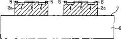
首先参阅图1所示,将经过测试以及切割过的晶片经过筛选品质检验合格的芯片,选取测试合格的芯片(die)1a,通过吸取与放置装置,将其重新排列配置于一新的玻璃底座1,该底座1可以是玻璃、陶瓷或硅晶片,并经由粘着剂将各个芯片1a粘着于底座1上,该粘着剂厚度大约10μm,固化粘着剂的过程是利用旋涂机进行粘着动作。芯片1a摆上于玻璃底座1,芯片1a间的距离加大,其目的是希望在后续封装过程中,具有充足的空间能够容纳扩散型圆锡球阵列。此扩散型封装技术可以提升I/O数目,或是在芯片1a尺寸缩小情形下,仍保持其理想间距,以防止I/O间的讯号干扰。封装的大小面积取决于后续制程完成后扩散型圆锡球阵列之间的间距大小而定。First, as shown in Figure 1, the tested and cut wafers are screened and qualified for quality inspection, and the qualified chips (die) 1a are selected, and rearranged and configured on a new glass base by a pick-up and place device. 1. The base 1 can be a glass, ceramic or silicon wafer, and each
在另一实施例中,该玻璃基座1上也可以包含电容1b配置于芯片1a的一侧,以提升滤波效果,如图2所示。In another embodiment, the glass base 1 may also include a
以下所述封装过程是从具有金属垫(metal pad)的单一芯片开始其封装过程:The packaging process described below starts with a single chip with a metal pad:
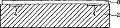
如图3所示,将进行封装的晶片2正面(或第一表面)具有做为输入输出的金属垫,例如铝垫(I/O pad or aluminum pad)4,该金属垫4是做为内连线用,利用光罩经过校准、曝光与显影过程,将金属垫4形成于晶片2的上面。As shown in Figure 3, the front side (or first surface) of the
接着,在晶片2上通过旋转涂布机旋涂一层BCB绝缘层8于晶片2与铝垫4的上面,以保护晶片2,BCB 8的厚度大约为5-10μm。Then, on the
接着,如图4所示,经过光罩校准、曝光与显影过程,去除部分的BCB 8,形成第一开口9,以曝露出下方的金属铝垫4,值得注意的是,此切割道上亦被暴露,且大于其切割道的宽度,以利于切割时不损及BCB。之后,以电镀方式形成化镍或化金11于铝垫4之上。Next, as shown in FIG. 4 , after mask alignment, exposure and development processes, part of the
经过切割,如图5表示,将多个芯片2a(此处晶片业经切割形成芯片)经由筛选与品质检验合格后,经由具有吸附与放置功能的机械将芯片2a摆置于玻璃底座6上面,并通过粘着剂7粘着于玻璃底座6上面,接着在炉内予以固化。After dicing, as shown in Figure 5, after a plurality of
接着,如图6所示,全面性地在玻璃底座6、芯片2a、BCB 8与开口的铝垫4的上面全面性地填充一层第一环氧树脂(EPOXY)10。Then, as shown in FIG. 6, a layer of first epoxy resin (EPOXY) 10 is comprehensively filled on the
接着,如图7所示,经过掩膜型蚀刻或化学药剂,移除铝垫4上方的第一环氧树脂10,形成第二开口13,并曝露出下方的铝垫4。接着,在炉内予以固化,此第一环氧树脂10的厚度大约为10-25μm之间(这里的厚度指的是芯片表面上的厚度)。Next, as shown in FIG. 7 , the first
接着,将剩余的环氧树脂,以RIE等离子体清洁芯片2a表面。至于上述的剩余的环氧树脂则以10’表示。上述的镍/金或化镍层11做为阻挡层或是粘着层的功用。Next, use RIE plasma to clean the surface of the
接着,如图8所示,在镍/金或化镍层11上方的第二开口13内利用焊锡12以丝网印刷技术填满该第二开口13。接着,以红外线回流固化此焊锡12,然后,全面性地溅镀一层钛/铜19于剩余的环氧树脂10’与焊锡12的上面,以作为铜籽晶层。Next, as shown in FIG. 8 , the
接着,如图9所示,以掩膜(未图示)定义铜导线图案,利用电镀方式形成铜导线于钛/铜19的上面,一端对准第二开口焊锡12的内端(芯片的内侧边),而另一端以水平方向朝外扩散(芯片的内侧边)。明确的讲,也就是说铜导线14的位置,一端是与铝垫4切齐,另一端以水平向方向朝外扩散来牵引导线,其与下层环氧树脂10’及焊锡12的接触面积较铝垫4的开口大,其目的主要是用来增加I/O的植球区域面积,接着,在铜导线14上面形成一层化镍层或化金层17,以做为后续焊锡植球的粘着层,再移除掩膜。并移除暴露于剩余环氧树脂10’的上面部分钛/铜19。Next, as shown in Figure 9, define the pattern of copper wires with a mask (not shown), utilize electroplating to form copper wires on the top of the titanium/copper 19, and one end is aligned with the inner end of the second opening solder 12 (inner of the chip) side), while the other end spreads outward in a horizontal direction (the inner side of the chip). To be clear, that is to say, the position of the
接着,如图10所示,全面性地涂布一层第二环氧树脂16于铜导线14、镍层17与下层环氧树脂10’的上面,并以固化的步骤,利用紫外线照射或加热处理,以硬化上述的第二环氧树脂,防止铜导线14被氧化。Next, as shown in FIG. 10 , coat a layer of second epoxy resin 16 on the top of
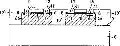
接着,如图11所示,去除铜导线14与镍层17上面的部分第二环氧树脂16,并形成第三开口15,该第三开口15的位置是在铜导线14与镍层17的上面,且尽可能位于铜导线14的外侧(远离铝垫4的一边),以利于制作扩散型(fan out)I/O结构。Then, as shown in FIG. 11 , remove the part of the second epoxy resin 16 above the
如图12所示,接着在第三开口15处,镍(Ni)层17的上面,通过丝网印刷技术或植球技术植入焊锡球18,由图中明显可见,焊锡球18经过一封装过程设计后的位置,并不在金属垫4的正上方,而是水平向侧伸到金属垫4的侧边上。As shown in Figure 12, then at the third opening 15, on the top of the nickel (Ni) layer 17,
接着,如图13所示,再经过红外线回流烘烤环氧树脂,晶片再传送至晶片型态测试装置中进行晶片型态测试,例如最后测试以及切割过程,并切割芯片与芯片间切割线20与玻璃基座6,以分离个别的封装体。Next, as shown in Figure 13, the epoxy resin is baked by infrared reflow, and the wafer is then transferred to the wafer type testing device for wafer type testing, such as the final test and cutting process, and the cutting
本发明的制程较传统技术简单,在未分割前,以晶片型态进行测试,且在测试后可以沿着切割道切划成个别的芯片,以吸取放置装置被置于玻璃基板之上,完成晶片型态扩散型封装(wafer level fan out packaging)。The manufacturing process of the present invention is simpler than the traditional technology. Before splitting, the test is carried out in the form of a wafer, and after the test, it can be cut into individual chips along the dicing line, and placed on the glass substrate with a pick-up and place device, and the chip is completed. Wafer level fan out packaging.
如图14所示,为镍/金或化镍层11、钛/铜或镍/金19、镍层17各粘着层与阻挡层,在内连线的各个位置示意图。As shown in FIG. 14 , it is a schematic diagram of the respective positions of the interconnection lines for each adhesion layer and barrier layer of the nickel/gold or
图15所示,为单一芯片的晶片型态扩散型封装成型的剖面示意图。As shown in FIG. 15 , it is a schematic cross-sectional view of the wafer-type diffusion packaging molding of a single chip.
本发明也能将芯片电容2b纳入封装过程,图16所示,为电容2b植入到玻璃基座上与单一芯片的晶片型态扩散型封装的剖面示意图。The present invention can also incorporate the
在另一实施例中,本发明也能将多芯片或多种被动组件整合纳人封装过程,图17所示,即为多芯片的封装过程中,晶片型态扩散型封装的剖面示意图,图中2a、2c代表不同的芯片,此种封装方式可将多芯片与多种被动组件整合封装,形成系统式封装(system in package)。In another embodiment, the present invention can also integrate multi-chips or various passive components into the packaging process, as shown in FIG. 17, which is a schematic cross-sectional view of a wafer-type diffusion package during the multi-chip packaging process. 2a and 2c represent different chips. This packaging method can integrate and package multiple chips and various passive components to form a system in package.
本发明的主要特征是基于晶片型态封装,并使用扩散型(fan out)方式将芯片表面I/O植球的位置侧向延伸,其优点可以增加I/O植球的数目;可以减少由于接触点距过于接近所造成的讯号干扰问题。The main feature of the present invention is based on wafer type encapsulation, and uses diffusion type (fan out) mode to extend the position of chip surface I/O planting ball laterally, its advantage can increase the number of I/O planting ball; Can reduce due to Signal interference caused by too close contact points.
本发明的主要优点如下:The main advantages of the present invention are as follows:
1、如图1所示,本发明的晶片型态封装的成本较传统技术低,再通过己测试及切割过的晶片经过筛选,将品质检验合格的芯片,选取好的芯片,通过吸取与放置的动作重新排列于一新的玻璃底座,可以减少制作成本,完成扩散型封装。1. As shown in Figure 1, the cost of the chip type packaging of the present invention is lower than that of the traditional technology, and then the tested and cut wafers are screened, and the chips that pass the quality inspection are selected, and the chips are picked and placed. The actions are rearranged on a new glass base, which can reduce the production cost and complete the diffusion package.
2、由于尺寸缩小原则,芯片亦随之缩小,而为了使得芯片间的距离仍然保持理想的距离(以不影响到讯号传递耦合为原则),在本发明中是以晶片型态扩散型封装,将I/O线向外扩散,并将连线拉到芯片外的区域,以增加焊锡圆球的数目及维持理想芯片间的距离。2. Due to the principle of size reduction, the chip is also reduced accordingly, and in order to keep the distance between the chips at an ideal distance (with the principle of not affecting the signal transmission coupling), in the present invention, the chip type diffusion type packaging is used. Diffuse the I/O lines outward and pull the wiring to the area outside the chip to increase the number of solder balls and maintain the ideal distance between chips.
3、本发明可以应用到8寸与12寸晶片的封装过程。3. The present invention can be applied to the packaging process of 8-inch and 12-inch wafers.
4、本发明可以整合芯片与电容于同一封装单体。4. The present invention can integrate the chip and the capacitor in the same packaging unit.
5、本发明能将多芯片或多种被动组件整合于同一单体,例如中央处理器、DRAM,SRAM等在封装底座的封装过程。5. The present invention can integrate multiple chips or multiple passive components into the same single body, such as the packaging process of the central processing unit, DRAM, SRAM, etc. in the packaging base.
6、本发明能将环氧树脂中的焊锡当作缓冲区,在后续制程中,减少不同层之间由于材质使用的不同所引发的应力不平衡问题,增加其可靠度。6. The present invention can use the solder in the epoxy resin as a buffer zone to reduce the stress imbalance problem caused by different materials used between different layers in the subsequent process, and increase its reliability.
7、本发明的底座是玻璃,其材质与芯片底材相同,由于材质中均含有硅材质,两者具有同样的热力膨胀系数(TCE),不会产生应力不平衡现象。7. The base of the present invention is glass, and its material is the same as that of the chip substrate. Since the material contains silicon material, the two have the same thermal expansion coefficient (TCE), and stress imbalance will not occur.
8、本发明的底座可以使用玻璃、灰石与硅晶片,以改善其可靠度。8. The base of the present invention can use glass, limestone and silicon wafers to improve its reliability.
9、本发明的封装机械都是以现有机械设备进行封装,可以省去额外添购的费用。9. The packaging machine of the present invention is packaged with existing mechanical equipment, which can save the cost of additional purchases.
10、本发明可以增加焊锡圆球的数目,其中有些焊锡圆球当作样本假输出输入端(dummy ball),此dummy ball虽无讯号传递的功能,却可供作缓冲区,以减弱不同材质间的应力,减少封装时芯片龟裂的现象发生。10. The present invention can increase the number of solder balls, some of which are used as dummy balls for sample output and input. Although the dummy ball has no function of signal transmission, it can be used as a buffer to weaken the effect of different materials. The stress between them can reduce the chip cracking during packaging.
本发明以较佳实施例说明如上,而熟悉此领域技艺者,在不脱离本发明的精神范围内,所作些许更动润饰,都属于本发明的保护范围之内。The present invention is described above with preferred embodiments, and those skilled in the art can make some changes and modifications without departing from the spirit of the present invention, all of which belong to the protection scope of the present invention.
Claims (25)
Priority Applications (1)
| Application Number | Priority Date | Filing Date | Title |
|---|---|---|---|
| CNB021009813ACN1230897C (en) | 2002-01-10 | 2002-01-10 | Semiconductor package structure and manufacturing method thereof |
Applications Claiming Priority (1)
| Application Number | Priority Date | Filing Date | Title |
|---|---|---|---|
| CNB021009813ACN1230897C (en) | 2002-01-10 | 2002-01-10 | Semiconductor package structure and manufacturing method thereof |
Publications (2)
| Publication Number | Publication Date |
|---|---|
| CN1431708A CN1431708A (en) | 2003-07-23 |
| CN1230897Ctrue CN1230897C (en) | 2005-12-07 |
Family
ID=4739546
Family Applications (1)
| Application Number | Title | Priority Date | Filing Date |
|---|---|---|---|
| CNB021009813AExpired - LifetimeCN1230897C (en) | 2002-01-10 | 2002-01-10 | Semiconductor package structure and manufacturing method thereof |
Country Status (1)
| Country | Link |
|---|---|
| CN (1) | CN1230897C (en) |
Families Citing this family (12)
| Publication number | Priority date | Publication date | Assignee | Title |
|---|---|---|---|---|
| US7459781B2 (en)* | 2003-12-03 | 2008-12-02 | Wen-Kun Yang | Fan out type wafer level package structure and method of the same |
| US7267861B2 (en)* | 2005-05-31 | 2007-09-11 | Texas Instruments Incorporated | Solder joints for copper metallization having reduced interfacial voids |
| CN101447437B (en)* | 2007-11-27 | 2010-06-02 | 南茂科技股份有限公司 | Use of preconfigured fan-out structures in die-reconfigured package structures |
| CN101452863B (en)* | 2007-11-28 | 2010-07-28 | 南茂科技股份有限公司 | Manufacturing method using compliant layer in package structure with reconfigured crystal grains |
| CN102044447B (en)* | 2009-10-20 | 2013-01-02 | 日月光半导体制造股份有限公司 | Packaging process and packaging structure |
| CN102254834B (en)* | 2010-05-18 | 2016-04-27 | 异基因开发有限责任公司 | Semiconductor package and method |
| CN102348328B (en)* | 2011-09-15 | 2015-05-13 | 深南电路股份有限公司 | Chip embedding method and chip-embedded circuit board |
| CN103151316B (en)* | 2011-12-06 | 2017-10-20 | 北京大学深圳研究生院 | A kind of Expansion method of the reconfigurable operator array structure based on MCP package form |
| CN106298726A (en)* | 2015-05-27 | 2017-01-04 | 佳邦科技股份有限公司 | Semiconductor packaging structure and semiconductor packaging method |
| CN108511329B (en)* | 2018-06-15 | 2024-03-15 | 德阳帛汉电子有限公司 | Chip cleaning device |
| CN111606302A (en)* | 2020-06-04 | 2020-09-01 | 南通通富微电子有限公司 | Sorting method and sorting system for MEMS (micro-electromechanical systems) packaging bodies |
| CN118215391A (en)* | 2024-05-22 | 2024-06-18 | 上海壁仞科技股份有限公司 | Packaging structure and manufacturing method thereof |
- 2002
- 2002-01-10CNCNB021009813Apatent/CN1230897C/ennot_activeExpired - Lifetime
Also Published As
| Publication number | Publication date |
|---|---|
| CN1431708A (en) | 2003-07-23 |
Similar Documents
| Publication | Publication Date | Title |
|---|---|---|
| CN113140519B (en) | Wafer-Level Packaging Using Molded Interposer | |
| CN1296981C (en) | Manufacturing method of semiconductor device | |
| US7459729B2 (en) | Semiconductor image device package with die receiving through-hole and method of the same | |
| US8178964B2 (en) | Semiconductor device package with die receiving through-hole and dual build-up layers over both side-surfaces for WLP and method of the same | |
| US7812434B2 (en) | Wafer level package with die receiving through-hole and method of the same | |
| US7655501B2 (en) | Wafer level package with good CTE performance | |
| US6537848B2 (en) | Super thin/super thermal ball grid array package | |
| US8178963B2 (en) | Wafer level package with die receiving through-hole and method of the same | |
| US20080083980A1 (en) | Cmos image sensor chip scale package with die receiving through-hole and method of the same | |
| US20080136004A1 (en) | Multi-chip package structure and method of forming the same | |
| US20080157358A1 (en) | Wafer level package with die receiving through-hole and method of the same | |
| JP2008244437A (en) | Image sensor package with die receiving opening and method thereof | |
| CN101246897A (en) | Wafer level image sensor package with die receiving hole and method thereof | |
| JP2008252087A (en) | Semiconductor device package structure and method thereof | |
| US20080211075A1 (en) | Image sensor chip scale package having inter-adhesion with gap and method of the same | |
| CN1767162A (en) | Structure of Wafer Scale Package and Method of Forming It | |
| TW201812888A (en) | Method for fabricating semiconductor devices | |
| JP2008160084A (en) | Wafer level package with die receiving cavity and method thereof | |
| JP2009016839A (en) | Image sensor package using removable protective film and method of manufacturing image sensor package | |
| CN1230897C (en) | Semiconductor package structure and manufacturing method thereof | |
| US8138594B2 (en) | Semiconductor device and manufacturing method of a semiconductor device | |
| US20080157398A1 (en) | Semiconductor device package having pseudo chips | |
| TW531854B (en) | Wafer level fan-out packaging process | |
| CN1452217A (en) | Wafer type packaging and manufacturing method thereof | |
| US20110134612A1 (en) | Rebuilt wafer assembly |
Legal Events
| Date | Code | Title | Description |
|---|---|---|---|
| C10 | Entry into substantive examination | ||
| SE01 | Entry into force of request for substantive examination | ||
| C06 | Publication | ||
| PB01 | Publication | ||
| C10 | Entry into substantive examination | ||
| SE01 | Entry into force of request for substantive examination | ||
| C14 | Grant of patent or utility model | ||
| GR01 | Patent grant | ||
| CX01 | Expiry of patent term | ||
| CX01 | Expiry of patent term | Granted publication date:20051207 |