CN1229871C - Micro-LED arrays with enhanced light extraction - Google Patents
Micro-LED arrays with enhanced light extractionDownload PDFInfo
- Publication number
- CN1229871C CN1229871CCNB008166013ACN00816601ACN1229871CCN 1229871 CCN1229871 CCN 1229871CCN B008166013 ACNB008166013 ACN B008166013ACN 00816601 ACN00816601 ACN 00816601ACN 1229871 CCN1229871 CCN 1229871C
- Authority
- CN
- China
- Prior art keywords
- light
- emitting diode
- layer
- micro
- leds
- Prior art date
- Legal status (The legal status is an assumption and is not a legal conclusion. Google has not performed a legal analysis and makes no representation as to the accuracy of the status listed.)
- Expired - Lifetime
Links
- 238000003491arrayMethods0.000titleabstractdescription3
- 238000000605extractionMethods0.000titleabstract4
- 239000006185dispersionSubstances0.000claimsdescription51
- 239000000758substrateSubstances0.000claimsdescription40
- 239000004065semiconductorSubstances0.000claimsdescription25
- 229910052751metalInorganic materials0.000claimsdescription16
- 239000002184metalSubstances0.000claimsdescription16
- 230000004888barrier functionEffects0.000claimsdescription5
- 238000009413insulationMethods0.000claims1
- 238000000034methodMethods0.000abstractdescription24
- 230000001965increasing effectEffects0.000abstractdescription11
- 238000012545processingMethods0.000abstractdescription3
- 239000000463materialSubstances0.000description25
- 238000003892spreadingMethods0.000description15
- 238000009826distributionMethods0.000description14
- 229910052737goldInorganic materials0.000description14
- 230000007480spreadingEffects0.000description14
- 238000004519manufacturing processMethods0.000description7
- 229910052763palladiumInorganic materials0.000description7
- 238000001020plasma etchingMethods0.000description7
- 229910052697platinumInorganic materials0.000description7
- 238000013459approachMethods0.000description5
- 239000004020conductorSubstances0.000description5
- 229920000642polymerPolymers0.000description5
- HBMJWWWQQXIZIP-UHFFFAOYSA-Nsilicon carbideChemical compound[Si+]#[C-]HBMJWWWQQXIZIP-UHFFFAOYSA-N0.000description5
- 230000008901benefitEffects0.000description4
- 238000005530etchingMethods0.000description4
- 230000003993interactionEffects0.000description4
- 229910052759nickelInorganic materials0.000description4
- 230000000737periodic effectEffects0.000description4
- 229920002120photoresistant polymerPolymers0.000description4
- 229910052594sapphireInorganic materials0.000description4
- 239000010980sapphireSubstances0.000description4
- 229910010271silicon carbideInorganic materials0.000description4
- 229910000980Aluminium gallium arsenideInorganic materials0.000description3
- 229910045601alloyInorganic materials0.000description3
- 239000000956alloySubstances0.000description3
- 229910052709silverInorganic materials0.000description3
- 238000000992sputter etchingMethods0.000description3
- 238000003631wet chemical etchingMethods0.000description3
- 229910001218Gallium arsenideInorganic materials0.000description2
- 239000004793PolystyreneSubstances0.000description2
- VYPSYNLAJGMNEJ-UHFFFAOYSA-NSilicium dioxideChemical compoundO=[Si]=OVYPSYNLAJGMNEJ-UHFFFAOYSA-N0.000description2
- 230000000903blocking effectEffects0.000description2
- 238000005229chemical vapour depositionMethods0.000description2
- 238000000151depositionMethods0.000description2
- 238000001312dry etchingMethods0.000description2
- 230000000694effectsEffects0.000description2
- 230000002708enhancing effectEffects0.000description2
- 230000008020evaporationEffects0.000description2
- 238000001704evaporationMethods0.000description2
- 239000010408filmSubstances0.000description2
- 238000010438heat treatmentMethods0.000description2
- 150000002739metalsChemical class0.000description2
- 229920002223polystyrenePolymers0.000description2
- 230000005855radiationEffects0.000description2
- 238000004544sputter depositionMethods0.000description2
- 239000010409thin filmSubstances0.000description2
- 239000004593EpoxySubstances0.000description1
- XUIMIQQOPSSXEZ-UHFFFAOYSA-NSiliconChemical compound[Si]XUIMIQQOPSSXEZ-UHFFFAOYSA-N0.000description1
- 239000012080ambient airSubstances0.000description1
- 238000000149argon plasma sinteringMethods0.000description1
- -1but not limited toSubstances0.000description1
- 238000006243chemical reactionMethods0.000description1
- 229910052681coesiteInorganic materials0.000description1
- 239000002131composite materialSubstances0.000description1
- 238000007796conventional methodMethods0.000description1
- 230000008878couplingEffects0.000description1
- 238000010168coupling processMethods0.000description1
- 238000005859coupling reactionMethods0.000description1
- 229910052906cristobaliteInorganic materials0.000description1
- 230000001747exhibiting effectEffects0.000description1
- 239000011521glassSubstances0.000description1
- 238000002347injectionMethods0.000description1
- 239000007924injectionSubstances0.000description1
- 239000012212insulatorSubstances0.000description1
- 230000007246mechanismEffects0.000description1
- 239000004005microsphereSubstances0.000description1
- 239000002245particleSubstances0.000description1
- 230000037361pathwayEffects0.000description1
- 230000008569processEffects0.000description1
- 230000001902propagating effectEffects0.000description1
- 238000004064recyclingMethods0.000description1
- 238000011160researchMethods0.000description1
- 229910052710siliconInorganic materials0.000description1
- 239000010703siliconSubstances0.000description1
- 239000000377silicon dioxideSubstances0.000description1
- 235000012239silicon dioxideNutrition0.000description1
- 230000003595spectral effectEffects0.000description1
- 229910052682stishoviteInorganic materials0.000description1
- 238000012546transferMethods0.000description1
- 229910052905tridymiteInorganic materials0.000description1
Images


Classifications
- H—ELECTRICITY
- H10—SEMICONDUCTOR DEVICES; ELECTRIC SOLID-STATE DEVICES NOT OTHERWISE PROVIDED FOR
- H10H—INORGANIC LIGHT-EMITTING SEMICONDUCTOR DEVICES HAVING POTENTIAL BARRIERS
- H10H20/00—Individual inorganic light-emitting semiconductor devices having potential barriers, e.g. light-emitting diodes [LED]
- H10H20/80—Constructional details
- H10H20/81—Bodies
- H10H20/813—Bodies having a plurality of light-emitting regions, e.g. multi-junction LEDs or light-emitting devices having photoluminescent regions within the bodies
- H—ELECTRICITY
- H10—SEMICONDUCTOR DEVICES; ELECTRIC SOLID-STATE DEVICES NOT OTHERWISE PROVIDED FOR
- H10H—INORGANIC LIGHT-EMITTING SEMICONDUCTOR DEVICES HAVING POTENTIAL BARRIERS
- H10H20/00—Individual inorganic light-emitting semiconductor devices having potential barriers, e.g. light-emitting diodes [LED]
- H10H20/80—Constructional details
- H10H20/83—Electrodes
- H10H20/831—Electrodes characterised by their shape
- H—ELECTRICITY
- H10—SEMICONDUCTOR DEVICES; ELECTRIC SOLID-STATE DEVICES NOT OTHERWISE PROVIDED FOR
- H10H—INORGANIC LIGHT-EMITTING SEMICONDUCTOR DEVICES HAVING POTENTIAL BARRIERS
- H10H20/00—Individual inorganic light-emitting semiconductor devices having potential barriers, e.g. light-emitting diodes [LED]
- H10H20/80—Constructional details
- H10H20/81—Bodies
- H10H20/819—Bodies characterised by their shape, e.g. curved or truncated substrates
- H10H20/82—Roughened surfaces, e.g. at the interface between epitaxial layers
- H—ELECTRICITY
- H10—SEMICONDUCTOR DEVICES; ELECTRIC SOLID-STATE DEVICES NOT OTHERWISE PROVIDED FOR
- H10H—INORGANIC LIGHT-EMITTING SEMICONDUCTOR DEVICES HAVING POTENTIAL BARRIERS
- H10H20/00—Individual inorganic light-emitting semiconductor devices having potential barriers, e.g. light-emitting diodes [LED]
- H10H20/80—Constructional details
- H10H20/83—Electrodes
- H10H20/832—Electrodes characterised by their material
- H10H20/833—Transparent materials
Landscapes
- Led Devices (AREA)
Abstract
Description
Translated fromChinese本申请要求Thibeault等人于1999年12月3日申请的美国临时申请案第60/168,817号之权利。This application claims the benefit of US Provisional Application No. 60/168,817, filed December 3, 1999 by Thibeault et al.
技术领域technical field
本发明涉及一种发光二极管,更具体地说,涉及一种加强所述发光二极管的光放出的新结构。The present invention relates to a light emitting diode, and more particularly, to a new structure for enhancing the light emission of the light emitting diode.
背景技术Background technique
发光二极管(LEDs)为一种将电能转换为光的重要固态装置,该装置通常包含一半导体材料的活性层,其夹在两个相反地掺杂层之间。当一偏压施加到该掺杂层时,空穴及电子被注入该活性层且在其中复合而产生光。由该活性区所产生的光全向发射,并且从所有暴露面逸出该装置。该发光二极管的外壳通常用来将逸出的光导入一所要求的输出发射剖面。Light-emitting diodes (LEDs) are an important solid-state device that converts electrical energy into light. The device typically includes an active layer of semiconductor material sandwiched between two oppositely doped layers. When a bias voltage is applied to the doped layer, holes and electrons are injected into the active layer and recombine therein to generate light. Light generated by the active region is emitted omnidirectionally and escapes the device from all exposed faces. The housing of the LED is generally used to direct the escaping light into a desired output emission profile.
当半导体材料改进时,该些半导体装置的效率也有改进。新的发光二极管用像是GaN的材料制作,该材料提供了在紫外线到黄光光谱范围内的有效光照。许多新的发光二极管在转换电能到光时比传统的灯更有效率以及可更可靠。由于发光二极管改进了,其被预期可在许多应用中取代传统的灯,例如交通信号、室外及室内显示器、汽车头灯及尾灯、常规室内照明等等。As semiconductor materials improve, the efficiency of these semiconductor devices also improves. The new light-emitting diodes are made of materials like GaN, which provide efficient lighting in the ultraviolet to yellow spectral range. Many new light-emitting diodes are more efficient and may be more reliable at converting electrical energy to light than traditional lamps. As light-emitting diodes improve, they are expected to replace traditional lights in many applications, such as traffic signals, outdoor and indoor displays, automotive headlights and taillights, general interior lighting, and the like.
然而,传统的发光二极管的效率受限于其不能够发射所有由其活性层产生的光。当一发光二极管被通电时,由其活性层发射的光(全向地)以许多不同的角度到达发射面。典型的半导体材料与周围空气(折射指数n等于1.0)或封装的环氧树脂(n约为1.5)相比,具有一较高的折射指数(n约为2.2至3.8)。根据斯涅尔定律,光线在从一具有高折射指数的地方传播到一具有低折射指数的地方时,如该光线在某一临界角之内(相对于该曲面法线方向),将会穿过到达该指数较低的地方。该光线以大于临界角到达该曲面时则不会穿过,而会经历全内反射(TIR)。在一个发光二极管的情况下,该TIR光可不断地在该发光二极管中反射,直到其被吸收为止,或其可从不同于该发射面的表面逸出。由于此现象,大量由传统发光二极管所产生的光没有发射出去,而使效率降低。However, the efficiency of conventional light-emitting diodes is limited by their inability to emit all the light generated by their active layers. When a light emitting diode is energized, light emitted by its active layer (omnidirectionally) reaches the emitting surface at many different angles. Typical semiconductor materials have a higher index of refraction (n about 2.2 to 3.8) than ambient air (n about 1.0) or encapsulated epoxy (n about 1.5). According to Snell's law, when a ray travels from a place with a high refractive index to a place with a low refractive index, if the ray is within a certain critical angle (relative to the normal direction of the surface), it will pass through Over to the lower part of the index. When the ray reaches the surface at an angle greater than the critical angle, it does not pass through, but undergoes total internal reflection (TIR). In the case of a light emitting diode, the TIR light can be continuously reflected in the light emitting diode until it is absorbed, or it can escape from a surface different from the emitting surface. Due to this phenomenon, a large amount of light generated by conventional LEDs is not emitted, reducing efficiency.
一种降低TIR光的百分比的方法是要在发光二极管的表面上产生随机结构型式的光散射中心。[由Shnitzer等人提出,″30% External Quantum Efficiency fromSurface Textured,Thin Film Light Emitting Diodes″,Applied Physics Letters63,页2174-2176(1993)]。该随机结构是在反应离子蚀刻期间,藉由使用亚微米直径聚苯乙烯颗粒在该发光二极管表面上做为一掩模而成型于该表面上。该结构化的表面具有在光的波长方面的特点,以致光的折射及反射的方式由于该随机干扰效应而无法由斯涅尔定律来预测。此方法显示可将发射效率改善9%到30%。One way to reduce the percentage of TIR light is to create a random pattern of light scattering centers on the surface of the LED. [Proposed by Shnitzer et al., "30% External Quantum Efficiency from Surface Textured, Thin Film Light Emitting Diodes", Applied Physics Letters 63, pages 2174-2176 (1993)]. The random structure is formed on the surface of the LED by using submicron diameter polystyrene particles on the surface as a mask during reactive ion etching. The structured surface has characteristics with respect to the wavelength of light such that light is refracted and reflected in a manner that cannot be predicted by Snell's law due to the stochastic interference effect. This approach has been shown to improve emission efficiency by 9% to 30%.
该表面结构的一个缺点在于其在该些具有较差导电性的电极层构造的发光二极管,例如p-型GaN,该表面结构可妨碍有效的电流分散。在较小的装置或具有良好导电性的装置中,来自该p及n型层接触点的电流可流入传遍各个层。而对于较大的装置或以较差导电性材料制成的装置,电流无法由该接触点传遍各个层。因此,部份该活性层不能接收到该电流而不能发射光。为了要在整个二极管区域产生均匀的电流注入,一导电材料分散层可沉积在其表面上。然而,此分散层通常必须是透光的以便光线能够透过该层。当一随机表面结构被引进到该发光二极管表面上时,则不能轻易地沉积一足够薄且透光的电流分散层。A disadvantage of this surface structure is that in light-emitting diodes where it is constructed on electrode layers with poor conductivity, such as p-type GaN, this surface structure can prevent effective current spreading. In smaller devices or devices with good electrical conductivity, current from the p- and n-type layer contacts can flow through the various layers. However, for larger devices or devices made of poorly conductive materials, the current cannot pass through the various layers from this contact point. Therefore, part of the active layer cannot receive the current and cannot emit light. In order to produce a uniform current injection over the entire diode area, a dispersed layer of conductive material can be deposited on its surface. However, the distribution layer must generally be transparent in order for light to be able to pass through the layer. When a random surface structure is introduced onto the LED surface, it is not easy to deposit a sufficiently thin and transparent current spreading layer.
另一个增加一发光二极管的光放出的方法为包含一在该发射表面或内部界面的周期图案,其可将光线从其内部的补捉角以由该表面形状及图案来确定的限定模式来重新导向。请参考授予Krames等人的美国专利号5,779,924。此技术为一随机结构表面的一特殊例,其中该干扰效应不再是随机的,而该表面可将光耦合到特殊的模式或方向。此方法的一个缺点是该结构很难制造,因为该表面形状及样式必须是均匀的,并且非常小,小至相当于该发光二极管光的单一波长。该图案也为沉积一透光的电流分散层带来困难,如前所述。Another approach to increasing the light emission of an LED is to include a periodic pattern on the emitting surface or internal interface that redirects light from its internal capture angle in a defined pattern determined by the surface shape and pattern. guide. See US Patent No. 5,779,924 to Krames et al. This technique is a special case of a randomly structured surface where the interference effect is no longer random and the surface can couple light into specific modes or directions. A disadvantage of this method is that the structure is difficult to fabricate because the surface shape and pattern must be uniform and very small, as small as a single wavelength of light from the LED. This pattern also makes it difficult to deposit a light-transmitting current spreading layer, as previously described.
要增加光放出也可通过将该发光二极管的放射面做成一在中心具有一放射层的半球形。在此结构增加放射光的量的同时,其的制作也很难。给Scifres及Burnham的美国专利号3,954,534中,揭示了形成一种发光二极管的阵列,在每个发光二极管之上分别有一半球形。该半球形系形成于一基板中,而二极管阵列于其上增长。然后,该二极管及透镜结构从该基板上蚀刻去除。此方法的缺点是其限于将该结构形成在该基板介面,而从该基板移除该结构会造成制造成本的增加。同时,每个半球皆有一放射层直接地位于其上,其需要非常精密的制造。The light emission can also be increased by making the emitting surface of the LED a hemispherical shape with an emitting layer in the center. While this structure increases the amount of emitted light, it is also difficult to fabricate. US Patent No. 3,954,534 to Scifres and Burnham discloses forming an array of LEDs with a respective hemisphere above each LED. The hemisphere is formed in a substrate on which the diode array is grown. Then, the diode and lens structures are etched away from the substrate. A disadvantage of this method is that it is limited to forming the structure at the substrate interface, and removing the structure from the substrate increases manufacturing costs. Also, each hemisphere has an emissive layer directly above it, which requires very precise fabrication.
美国专利号5,793,062揭示一种结构,其用于加强自一发光二极管的光放出,藉由包含不吸光的非吸收层来将光重新导向离开吸收区域,例如接触点,并且还使光朝该发光二极管的表面方向改向。此结构的一个缺点是,该非吸收层需要形成削底的狭角层,对许多材料体系而言非常难以制造。U.S. Patent No. 5,793,062 discloses a structure for enhancing light emission from a light-emitting diode by including non-absorbing non-absorbing layers to redirect light away from absorbing regions, such as contact points, and also direct light toward the emitting diode. The surface direction of the diode is redirected. A disadvantage of this structure is that the non-absorbing layer needs to be formed as a bottomed narrow angle layer, which is very difficult to manufacture for many material systems.
加强光放出的另一个方法是在该发光二极管的发射面上的一薄膜金属层之内将光子耦合到表面等离子体振子模式,该些光子被发射回到辐射模式。[Knock等人的,″Strongly Directional Emission from AlGaAs/GaAs Light EmittingDiodes″,Applied Physics Letter 57,页2327-2329,(1990)]。这些结构依赖将该半导体发射回来的光子耦合到该金属层中的表面等离子体振子,其进一步与最终被放出的光子耦合。此装置的一个缺点是,其很难制造,因为该周期结构为一沟深极浅(<0.1微米)的单维刻划光栅。同时,总体外部量子效率很低(1.4-1.5%),很可能是由于光子到表面等离子体振子以及表面等离子体振子到环境光子转换机制的效率低。此结构也会带来与一电流分散层有关的同样的困难,如上所述。Another approach to enhance light emission is to couple photons into surface plasmon modes within a thin-film metal layer on the emitting face of the LED, which photons are emitted back into radiation mode. [Knock et al., "Strongly Directional Emission from AlGaAs/GaAs Light Emitting Diodes", Applied Physics Letter 57, pp. 2327-2329, (1990)]. These structures rely on the coupling of photons emitted back from the semiconductor to surface plasmons in the metal layer, which are further coupled to the eventually emitted photons. A disadvantage of this device is that it is difficult to fabricate since the periodic structure is a one-dimensional ruled grating with very shallow groove depth (<0.1 microns). At the same time, the overall external quantum efficiency is low (1.4–1.5%), most likely due to the inefficiency of the photon-to-surface plasmon and surface plasmon-to-ambient photon conversion mechanisms. This structure also presents the same difficulties associated with a current spreading layer, as described above.
要改善光放出还可藉由使发光二极管片的侧面成某一角度以产生一倒置的截顶锥形。该成某一角度的表面提供了一在临界角之内的放射面给截留于该基板材料中的TIR光线[Krames等人的,’High Power Truncated Inverted Pyramid(AlxGal-x)0.5In0.5P/GaP Light Emitting Diodes Exhibiting>50% ExternalQuantum Efficiency’,Applied Physics Letters 75(1999)]。藉由此方法,对于InGaAlP材料体系来说,所展示的外部量子效率增加了35%到50%。此方法对于将大量光截留于该基板中的装置来说是可行的。至于在蓝宝石基板上成长GaN的情况下,大量光是被截留于GaN膜中,所以使发光二极管片的侧面成某一角度并不能达到所要求的增益。Light emission can also be improved by angling the sides of the LED chip to create an inverted truncated cone. The angled surface provides a radiation surface within the critical angle to the TIR rays trapped in the substrate material [Krames et al., 'High Power Truncated Inverted Pyramid (AlxGal-x) 0.5In0.5P/ GaP Light Emitting Diodes Exhibiting>50% External Quantum Efficiency', Applied Physics Letters 75(1999)]. By this method, an increase in the external quantum efficiency of 35% to 50% was demonstrated for the InGaAlP material system. This approach is feasible for devices that trap a large amount of light in the substrate. As in the case of growing GaN on a sapphire substrate, a large amount of light is trapped in the GaN film, so angling the sides of the LED chip does not achieve the desired gain.
另有一种加强光放出的方法是光子循环利用[Shnitzer等人的,’Ultrahighspontaneous emission quantum efficiency,99.7% internally and 72%externally,from AlGaAs/GaAs/AlGaAs double heterostructures’,AppliedPhysics Letters 62,页131-133,(1993)]。此方法依靠具有一高效率活性层的发光二极管,该活性层可立即将电子及空穴转换成光,反之亦然。TIR光由该发光二极管表面反射出来,并撞击到该活性层,从而转换回到一电子-空穴对。由于该活性层的高效率,该电子-空穴对几乎立即转换为光,并再次向随机方向发射。某一百分比的循环利用光将会以小于临界角来打在发光二极管的其中一个发射面而逸出。而反射回到该活性层的光会再次经历同样的过程。然而,此方法仅能够用于以光损耗非常低的材料制成的发光二极管,而不能够用于在其表面上具有一吸收电流分散层的发光二极管。Another way to enhance light emission is photon recycling [Shnitzer et al., 'Ultrahighspontaneous emission quantum efficiency, 99.7% internally and 72% externally, from AlGaAs/GaAs/AlGaAs double heterostructures', AppliedPhysics Letters 62, pp. 131-133 , (1993)]. This approach relies on light-emitting diodes with a high-efficiency active layer that instantly converts electrons and holes into light and vice versa. TIR light is reflected off the surface of the LED and strikes the active layer, where it is converted back into an electron-hole pair. Due to the high efficiency of the active layer, the electron-hole pairs are converted into light almost immediately and emitted again in random directions. A certain percentage of recycled light will escape by hitting one of the emitting surfaces of the LED at an angle less than the critical angle. Light reflected back to the active layer goes through the same process again. However, this method can only be used for light-emitting diodes made of materials with very low light losses, and not for light-emitting diodes that have a sinking current-dispersing layer on their surface.
发明内容Contents of the invention
本发明提供一种新的发光二极管,其具有互连的微发光二极管阵列,以提供改善的光放出。微发光二极管具有一较小的活性区,其范围在1到2500平方微米,但该大小并非本发明的关键。一微发光二极管的阵列为任何以电互连的微发光二极管分布。该阵列提供一大的表面积,使光能够逸出每个微发光二极管,此而增加发光二极管的可用光。所述新发光二极管可具有许多不同的几何形状,且由于其是以标准半导体处理技术来形成,故非常易于制造。The present invention provides a new light emitting diode having an array of interconnected micro light emitting diodes to provide improved light emission. Micro LEDs have a small active area ranging from 1 to 2500 square microns, but this size is not critical to the invention. An array of micro LEDs is any distribution of micro LEDs that are electrically interconnected. The array provides a large surface area to enable light to escape each microLED, thereby increasing the available light of the LED. The new light-emitting diodes can have many different geometries and are very easy to manufacture because they are formed with standard semiconductor processing techniques.
该新发光二极管包含一第一导电分散层,其的一个表面上沉积有若干微发光二极管。每个微发光二极管皆具有一p-型层,一n-型层及一夹在所述p-及n-型层之间的活性层。所述p-或n-型层皆可为上层,而另一个则可为下层。施加于所述第一分散层的电流会分散到每个微发光二极管的下层。一第二分散层包含在所述微发光二极管上,而自所述第二分散层的电流会分散到所述上层。当一偏压施加在所述第一及第二分散层时,微发光二极管即发光。The new light emitting diode comprises a first conductive dispersion layer, on one surface of which a number of micro light emitting diodes are deposited. Each micro light emitting diode has a p-type layer, an n-type layer and an active layer sandwiched between the p-type and n-type layers. Either the p- or n-type layer can be the upper layer, while the other can be the lower layer. The current applied to the first distribution layer will be distributed to the lower layer of each micro light emitting diode. A second distribution layer is included on the micro-LED, and the current from the second distribution layer is distributed to the upper layer. When a bias voltage is applied to the first and second dispersion layers, the micro light emitting diodes emit light.
所述第二分散层的一实施例为一导电的互连的栅格状结构,其具有在所述微发光二极管上的导电通路,该些通路与所述微发光二极管的上层接触。一绝缘层包含在所述阵列上,而所述栅格在该绝缘层上,因此将所述第一分散层与所述栅格电绝缘。One embodiment of the second dispersion layer is a conductive interconnected grid-like structure with conductive vias on the micro-LEDs, the vias being in contact with the upper layer of the micro-LEDs. An insulating layer is included on the array and the grid is on the insulating layer, thereby electrically insulating the first dispersion layer from the grid.
另外,可用倒装片接合使微发光二极管互连。使用此方法,首先形成一未连接的微发光二极管阵列,然后使其接合到一导电性材料以使该阵列互连。在一第三实施例中,所述栅格通过微发光二极管,而且所述p-型、活性层、及n-型材料在该些微发光二极管之间的栅格的导电通路之下以将该栅格及第一分散层电绝缘。此栅格状结构可被设计来使发射的光能够在传播一段短距离之后与一侧壁互相作用。In addition, flip-chip bonding can be used to interconnect micro-LEDs. Using this method, an array of unconnected micro LEDs is first formed and then bonded to a conductive material to interconnect the array. In a third embodiment, the grid passes through the micro LEDs, and the p-type, active layer, and n-type materials are under the conductive pathways of the grid between the micro LEDs so that the The grid and the first distribution layer are electrically insulated. This grid-like structure can be designed to allow emitted light to interact with one side wall after traveling a short distance.
所述新发光二极管能够使光放出组件(LEEs)沉积在该些微发光二极管之间,或是形成在该些微发光二极管的侧面之上,以进一步加强光放出。该些LEEs用来使在一标准发光二极管结构中的光线转向或聚焦,否则光线将会通过TIR被截留或吸收。LEEs的形状可以是曲面的(凸出或凹入),或是片段线性的,而该结构的形状会影响光放出以及光的最终放出方向。在所述微发光二极管之间的LEEs与从该微发光二极管侧面逸出的光相互作用。此相互作用有助于防止反射回到该发光二极管的光被吸收,因此增加了由该发光二极管出来的有用光。The new LEDs enable light emitting elements (LEEs) to be deposited between the micro-LEDs or formed on the sides of the micro-LEDs to further enhance light emission. The LEEs are used to turn or focus light in a standard LED structure that would otherwise be trapped or absorbed by TIR. The shape of LEEs can be curved (convex or concave), or segmented linear, and the shape of the structure affects light emission and the final direction of light emission. The LEEs between the micro-LEDs interact with light escaping from the sides of the micro-LEDs. This interaction helps prevent light reflected back to the LED from being absorbed, thus increasing the useful light coming out of the LED.
通过以下的详细叙述并且结合附图,本领域的技术人员就会明白本发明的这些以及其它进一步的特征和优点,其中:Those skilled in the art will understand these and other further features and advantages of the present invention through the following detailed description and in conjunction with the accompanying drawings, wherein:
附图说明Description of drawings
图1所示为一具有一微发光二极管阵列的新发光二极管的平面图,该微发光二极管阵列具有一在一电绝缘层上的互连电流分散栅格;Figure 1 shows a plan view of a novel light emitting diode having an array of micro light emitting diodes with an interconnected current spreading grid on an electrically insulating layer;
图2所示为图1中该新发光二极管沿截面线2-2的剖面图;Figure 2 is a cross-sectional view of the new light-emitting diode in Figure 1 along section line 2-2;
图3所示为该新发光二极管的另一实施例的剖面图,其微发光二极管阵列是利用倒装式安装接合到一次固定层的;Figure 3 is a cross-sectional view of another embodiment of the new light-emitting diode, in which the micro-light-emitting diode array is bonded to the primary fixed layer by flip-chip mounting;
图4所示为该新发光二极管的一第三实施例的导电互连电流分散栅格和在该格栅通路下面的半导体材料的平面图;Figure 4 is a plan view of a conductive interconnect current spreading grid and semiconductor material underlying the grid vias of a third embodiment of the new light emitting diode;
图5所示为图4中该发光二极管沿截面线4-4的剖面图;FIG. 5 is a cross-sectional view of the light-emitting diode along section line 4-4 in FIG. 4;
图6所示为另一互连电流分散栅格的平面图;Figure 6 is a plan view of another interconnected current spreading grid;
图7所示为又一互连电流分散栅格的平面图;Figure 7 is a plan view of another interconnected current spreading grid;
图8所示为可在该微发光二极管之内结合的LEEs的基本形状的剖面图;Figure 8 is a cross-sectional view showing the basic shape of LEEs that can be incorporated within the micro-LED;
图9所示为具有在该些微发光二极管之间形成的不同的LEEs的该新发光二极管的剖面图,;Figure 9 is a cross-sectional view of the new LED with different LEEs formed between the micro LEDs;
图10所示为具有以随机形式构造表面的LEEs的该新发光二极管的剖面图;Figure 10 shows a cross-sectional view of the new light-emitting diode with LEEs whose surface is structured in a random pattern;
图11所示为图10中该微发光二极管阵列的剖面图,其具有一直接地位于该电流分散栅格下面的电流阻隔层;FIG. 11 is a cross-sectional view of the micro-LED array in FIG. 10, which has a current blocking layer directly below the current spreading grid;
图12所示为具有与微发光二极管的侧面成一体的LEEs的该新发光二极管的剖面图;Figure 12 shows a cross-sectional view of the new LED with LEEs integrated into the sides of the micro LED;
图13所示为具有与微发光二极管的侧面结合的曲面LEEs的该新发光二极管的剖面图;Figure 13 shows a cross-sectional view of the new LED with curved LEEs combined with the sides of the micro LED;
图14所示为具有与微发光二极管的侧面及中间结合的曲面LEEs的该新发光二极管的剖面图;及Figure 14 shows a cross-sectional view of the new LED with curved LEEs combined with the sides and the middle of the micro LED; and
图15所示为如图4中的但具有曲面的LEEs的该新发光二极管的剖面图。Figure 15 shows a cross-sectional view of the new LED as in Figure 4 but with curved LEEs.
具体实施方式Detailed ways
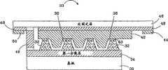
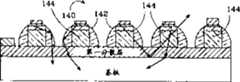
图1及2所示为根据本发明构造的该新发光二极管10的一实施例。该发光二极管包含一微发光二极管12的阵列,每个微发光二极管12皆被隔离,并具有其本身的夹在相反掺杂层16及18之间的半导体材料活性层14。在较佳的微发光二极管中,其上层16为p-型,而下层18为n-型,尽管将层16及层18相反地掺杂仍然可以运作。Figures 1 and 2 show an embodiment of the new LED 10 constructed in accordance with the present invention. The LED comprises an array of
该新发光二极管也包含一第一分散层20,其将电流由n-接触点22分散到每个微发光二极管的下层18。该接触点22称为n-接触点是由于在该较佳实施例中的下层18为n-型。一绝缘层23沉积在该微发光二极管阵列之上,其覆盖了每个微发光二极管以及在微发光二极管之间的沟槽中第一分散层的表面。一第二分散层,其最好以一互连电流分散栅格24的形式沉积在该绝缘层上,该绝缘层与栅格的导电通路在该些微发光二极管上横过。一p-接触点26沉积在该栅格24上,而从该接触点的电流通过该栅格分散到每个微发光二极管12的上层16。该接触点26称之为p-接触点,因为在该较佳实施例中的上层16为p-型。The new LED also comprises a first distribution layer 20 which distributes the current from the n-
一空穴形成于每个微发光二极管之上而穿过所述绝缘层,一微发光二极管接触点29包含在每个绝缘层空穴中以作为在栅格24和微发光二极管的上层16之间的接触点。所述微发光二极管(除了空穴之外)和所述第一分散层的表面通过所述绝缘层23与所述电流分散栅格电绝缘。整个结构在一基板28上形成且该些微发光二极管形成一阵列且在一偏压施加于接触点22及26时即发光。在另一实施例中,一透明导电片被用作为第二分散层来代替栅格24。A hole is formed above each micro-LED through the insulating layer, and a
该新发光二极管10具有增强的光放射,是因为其发射面通过该些隔离的微发光二极管而增加。由每个微发光二极管的活性层所产生的光仅在一小段距离之后即与该微发光二极管的边缘相互作用。如果该光在该临界角之内,其可从微发光二极管逸出,并对该发光二极管的光放射作出贡献。新发光二极管特别有利于某些发光二极管结构,在该些结构中的部份发射光由于在电流分散层与基板介面处的全内反射(TIR)而不能传播到基板。这种状况发生在蓝宝石、AlN、或MgO基板上基于GaN的发光二极管。The new LED 10 has enhanced light emission because its emitting surface is increased by the isolated micro LEDs. The light generated by the active layer of each micro-LED interacts with the edge of the micro-LED only after a short distance. If the light is within the critical angle, it can escape from the micro LED and contribute to the light emission of the LED. The new LEDs are particularly advantageous for certain LED structures in which part of the emitted light cannot propagate to the substrate due to total internal reflection (TIR) at the interface of the current spreading layer and the substrate. This situation occurs for GaN-based LEDs on sapphire, AlN, or MgO substrates.
新发光二极管10通过先沉积第一分散层20在基板28上来制造。然后,一具有一n-型、p-型及一活性层的外延生长的发光二极管结构在第一分散层20上形成。该微发光二极管是使用半导体蚀刻技术,例如湿式化学蚀刻,反应离子蚀刻(RIE),离子研磨,或任何其它用于移除半导体材料的技术,蚀刻去除部份发光二极管结构而形成的。A new light emitting diode 10 is fabricated by first depositing a first dispersion layer 20 on a
每个剩余的微发光二极管形成一独立及电绝缘的装置,其具有一由相反掺杂层16及18包围的活性层。该微发光二极管12的形状及位置皆可不同,每个微发光二极管的形状最好为圆柱形。当由上方观视时,每个微发光二极管呈现为圆形,其直径为1到50微米之间。该微发光二极管最好形成密集的结构以使可用的微发光二极管空间最大化。相邻微发光二极管之间的间距最好是在1到50μm的范围内,虽然该间距并非本发明的关键。绝缘器层23可由不同的方法来沉积在整个结构上,例如蒸发,化学气相沉积(CVD)或溅镀。然后在每个微发光二极管12上的绝缘层23中蚀出开口。微发光二极管接触点及导电栅格然后通过标准的沉积技术来沉积。Each remaining micro LED forms an independent and electrically isolated device having an active layer surrounded by oppositely doped
所述第一分散层20既可以是一沉积在基板上的导电层,又可是该基板本身,如果其是导电的话。基于GaN的发光二极管的较佳导电基板包含GaN或碳化硅(SiC)。SiC具有更密集的晶格而与III族氮化物相配,例如GaN,而且使III族氮化物薄膜具有高品质。碳化硅也具有一非常高的热导率,所以在碳化硅上的III族氮化物装置的整体输出功率不受限于该基板的热耗散(像一些在蓝宝石上形成的装置通常就会这样)。SiC基板可由美国North Carolina,Durham的Cree Research公司获得,其制造方法被阐明于科学文献及美国专利,有关编号为34,861;4,946,547及5,200,022。The first dispersion layer 20 can be either a conductive layer deposited on the substrate, or the substrate itself, if it is conductive. Preferred conductive substrates for GaN-based light emitting diodes include GaN or silicon carbide (SiC). SiC has a denser lattice that matches III-nitrides, such as GaN, and enables high-quality III-nitride films. SiC also has a very high thermal conductivity, so the overall power output of a III-nitride device on SiC is not limited by the thermal dissipation of the substrate (as some devices formed on sapphire typically do. ). SiC substrates are available from Cree Research, Durham, North Carolina, USA, and their fabrication methods are described in the scientific literature and in US Patent Nos. 34,861; 4,946,547 and 5,200,022.
如果该基板为电流分散层,底部接触点可通过使在该基板上暴露的任何表面金属化而沉积。较佳的发光二极管具有微发光二极管12,其基于AlGaInN且以一p-型表面作为其上层16。该基板为蓝宝石,第一分散层为n-型AlGaInN(或其合金),而金属化接触点为Al/Ni/Au、Al/Ti/Au、或Al/Pt/Au。所述绝缘层23可由许多材料制成,例如,但不限于,SiN、SiO2、或AlN。If the substrate is a current spreading layer, the bottom contact can be deposited by metallizing any exposed surface on the substrate. The preferred LED has a
该栅格24可以是任何导电材料,包含金属、半金属、及半导体。其可由Al、Ag、Al/Au、Ag/Au、Ti/Pt/Au、Al/Ti/Au、Al/Ni/Au、Al/Pt/Au或其组合物来制成。另外,该栅格可由一薄的半透明金属来制成,例如Pd、Pt、Pd/Au、Pt/Au、Ni/Au、NiO/Au或其合金来制成。该栅格24可由许多传统的方法而沉积在所述新发光二极管上,而较佳的方法为蒸发或溅镀。在较佳实施例中,电流分散栅格24的通路宽度在1到10μm之间。微发光二极管接触点29可用Pt、Pt/Au、Pd、Pd/Au、Ni/Au、NiO、或NiO/Au制成。p-接触点26可以沉积在所述互连栅格24上的不同位置,以使来自接触点的电流可以传遍该栅格。The
图3所示为一根据本发明来构造的发光二极管30的第二实施例,其利用倒装式安装。如上所述,是通过蚀刻去除一完整发光二极管结构的半导体材料来形成一微发光二极管32阵列的。每个微发光二极管32具有一由两个相反掺杂层所包围的活性层。微发光二极管的配置及尺寸类似于上述的实施例。然而,在此实施例中,每个微发光二极管具有成某角度的侧面,其上层比其下层要窄。如上所述,微发光二极管阵列在一形成于一基板36上的第一分散层34上形成。一绝缘层38覆盖微发光二极管以及在相邻微发光二极管之间的第一分散层的表面。在每个微发光二极管32之上,一空穴包含在绝缘层中作为一上接触点40。一第二分散层42覆盖整个微发光二极管阵列以与上接触点40互连。FIG. 3 shows a second embodiment of a
第二分散层42在与微发光二极管相反的表面,通过一接合介质与一次固定层46上的反光金属层48接合。一p-接触点44包含于金属层48上,而施加到第二接触点的电流传遍第二分散层,到达上接触点40及微发光二极管32的上层。在所述金属层48中有一裂缝,n-接触层50在部份金属层48上形成,该部份与具有p-接触点的部份电绝缘。指形件49在次固定层和第一分散层之间接合,并且使自接触点50传到金属层48的电流可通过流该指形件到达第一分散层34。该电流再传遍第一分散层及到达微发光二极管的下层。The
在此倒装式实施例中,自发光二极管50的光发射主要通过基板36。第二分散层42可以是反光的以使从微发光二极管32向第二分散层42的方向发射的光可被反射到发光二极管的基板36。最好以Al或Ag作为第二分散层以及每个微发光二极管32是基于AlGaInN且有一p-型上层。每个上接触点40最好为Pt、Pt/Au、Pd、Pd/Au、Ni/Au、NiO或NiO/Au。In this flip-chip embodiment, light emission from
由于该些隔离的微发光二极管,此实施例增强了发射光与侧壁的相互作用。布置在微发光二极管之间的第二分散层42的部份做为LEEs,其使光由微发光二极管反射到基板。通过该次固定层,此架构还使该新发光二极管芯片的热力可更好地传出去。Due to the isolated micro LEDs, this embodiment enhances the interaction of the emitted light with the sidewalls. Portions of the
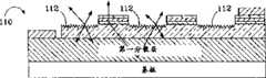
图4及5所示为该新发光二极管51的另一实施例,该新发光二极管并没有一隔开第一分散层及第二分散层的绝缘层。微发光二极管52是通过一互连栅格54的导电通路与相邻的微发光二极管连接,其中该通路的下面有半导体材料。每个栅格54中的开口55为一区域,其处的半导体材料在制造该发光二极管51时,从该发光二极管结构被蚀掉。该结构的剩余部份在该栅格54下为微发光二极管52,而在该些微发光二极管之间的栅格通路53下为半导体材料。微发光二极管及在该通路下的材料包含一由两个相反掺杂层包围的活性层,而整个结构则在一第一分散层56及一基板58之上形成。4 and 5 show another embodiment of the new light emitting diode 51 without an insulating layer separating the first dispersion layer and the second dispersion layer.
一沉积在第一分散层上的第一接触点60将电流施加到微发光二极管的下层,而一包含在电流分散栅格上的第二接触点62将电流分散到微发光二极管的上层。当施加一偏压到该接触点60及62时,电流被施加到该微发光二极管及在导电通路下的的半导体材料,使它们全部发光。光从该些通路下的微发光二极管材料的侧面逸出,避免了全内反射。因此本技术可以通用于在任何基板上的任何发光二极管结构以及可以用标准处理技术来实现。A
要制造发光二极管51首先要在基板58上沉积第一分散层56,然后再形成一连续的发光二极管结构,其将电流分散层56覆盖。栅格54沉积在该发光二极管结构上,而该发光二极管结构在该栅格开口中可见到的部份可以不同的方法来蚀除,例如湿式化学蚀刻、反应离子蚀刻(RIE)、离子研磨、或任何其它用于移除半导体材料的技术。部份的发光二极管结构也被蚀刻以提供一接触点60区域,使接触点60及62在其上沉积。栅格54可以任何导电材料来制造,包括但不限于金属、半金属、半导体、或其组合。微发光二极管最好基于GaN,而每个微发光二极管的上层55为一p-型AlGaInN或其任何合金,而栅格54最好以一薄金属来制造,例如Ni、Pd、Au、Pt或其任何组合。To manufacture the LED 51 , firstly, the
图4中的虚线示出微发光二极管其中之一以及该微发光二极管周围的区域,在其处可包含LEEs以进一步加强光放出,以下将会充分地叙述。The dashed lines in FIG. 4 show one of the micro-LEDs and the area around the micro-LED where LEEs may be included to further enhance light emission, as will be more fully described below.
图6及7所示为该新发光二极管的两个额外的实施例70和80,其具有不同的微发光二极管及栅格结构72及82,尽管还可用许多不同的结构。每一实施例具有一个别的下分散接触点73及83。在图6中,该互连的微发光二极管74通过不同的通路将电流交叉分散到每个微发光二极管。在每条通路下有半导体材料以使其与第一分散层隔离。栅格72提供呈正方阵列结构的开口以与光相互作用。Figures 6 and 7 show two
栅格54有一优于栅格72之处。在发光二极管70中,TIR光可沿栅格的许多的导电通路的其中之一反射以及可在不与该些微发光二极管的其中之一的表面相互作用下于该发光二极管之内反射。在该栅格中或在下层中的光耗将会造成某些TIR光在其逸出新发光二极管的最终边缘之前被吸收掉。栅格54将此问题减少,因为从微发光二极管发射的光在传播仅仅一短距离之后(最多为两个微发光二极管的长度)就到达一侧面,从而使逸出该装置的光增加。
在图7中,微发光二极管是随机性地成形以及具有随机的互连通路。此外,在该些通路下有半导体材料。该随机结构使TIR光在遇到其中一栅格开口中的其中一微发光二极管之前可供TIR光传播的通路数目降低。如上所述,在图6及7中环绕微发光二极管的虚线示出微发光二极管76及86和环绕在其周边的LEEs,以下将会充分地叙述。In FIG. 7, micro LEDs are randomly shaped and have random interconnection paths. In addition, there is semiconductor material under the vias. The random structure reduces the number of paths for the TIR light to travel before encountering one of the micro LEDs in one of the grid openings. As noted above, the dotted lines surrounding the microLEDs in FIGS. 6 and 7 illustrate microLEDs 76 and 86 and the LEEs surrounding their perimeters, as will be more fully described below.
开口尺寸及开口之间的距离最好在1到30μm之间,但可以较大或者较小。该开口的可以是非周期或周期结构,因为光与微发光二极管边缘的相互作用在本质上并不需要以上任一条件。在较佳实施例中,在一p-型AlGaInN层上的栅格开口的宽度在1微米到20微米之间,微发光二极管的宽度则在1微米到30微米之间。The size of the openings and the distance between the openings are preferably between 1 and 30 [mu]m, but can be larger or smaller. The openings can be non-periodic or periodic, since the interaction of light with the edge of the micro-LED does not inherently require either of these conditions. In a preferred embodiment, the width of the grid openings on a p-type AlGaInN layer is between 1 micron and 20 microns, and the width of the micro LEDs is between 1 micron and 30 microns.
先前的三个实施例全部都可与在微发光二极管之间的LEEs结合来进一步增加光发射。该LEEs既可在微发光二极管的侧面上,又可在第一分散层的表面形成,或者,在那些不具有第一分散层的实施例中则可在导电基板上形成。All three previous embodiments can be combined with LEEs between micro LEDs to further increase light emission. The LEEs can be formed either on the sides of the micro-LEDs, on the surface of the first dispersion layer, or, in those embodiments without the first dispersion layer, on the conductive substrate.
尽管可以使用其它的LEEs形状以及本发明的保护范围也不限于所示的形状,图8仍示出了若干可供选择的LEEs形状,该些形状包含在本发明的实施例中。LEEs82、84、86具有曲面,而LEEs 88、90、92、94则具有分段的线性表面。另外,该LEE可为一随机糙面层,其可做为一光弥散器。Although other LEEs shapes can be used and the scope of the invention is not limited to the shapes shown, Figure 8 shows several alternative LEEs shapes which are included in embodiments of the invention.
LEEs可用标准蚀刻技术来形成,例如湿式化学蚀刻,RIE,或离子研磨。在该较佳实施例中,LEEs是通过使用一商用的做为一烧蚀蚀刻掩模的聚合物来形成的(例如一紫外线或电子束敏感光阻)。此聚合物首先被沉积,并形成为类似方边的结构。该聚合物会加热到一个温度,并如玻璃般重熔以致该聚合物的边缘形成一逐渐线性或弯曲的形状。该聚合物厚度、结构形状、加热温度及加热时间将决定该边缘形状。该结构可以以RIE转换到基于AlGaInN的微发光二极管。用此方法可轻易地制造线性及曲形的LEEs,而通过使用多个蚀刻掩模可轻易地构造分段式线性LEEs。LEEs can be formed using standard etching techniques, such as wet chemical etching, RIE, or ion milling. In the preferred embodiment, LEEs are formed by using a commercially available polymer (eg, a UV or E-beam sensitive photoresist) as an ablative etch mask. The polymer is first deposited and formed into a square-edge-like structure. The polymer is heated to a temperature and remelts like glass so that the edges of the polymer form a gradually linear or curved shape. The polymer thickness, structural shape, heating temperature and heating time will determine the edge shape. This structure can be converted to AlGaInN-based micro-LEDs by RIE. Linear and curved LEEs can be easily fabricated by this method, and segmented linear LEEs can be easily constructed by using multiple etch masks.
用来形成LEEs的第二种技术是使用负极性UV可曝光光阻。首先,使该光阻持续曝光一特定的曝光时间,并将其加工以产生一负极性。然后使该光阻显影以在其截面产生一削底的弯曲或线性形状。然后此结构可经由一干式蚀刻技术转换到半导体材料。对这两个实施例而言,干式蚀刻的环境也会影响半导体材料中透镜的最终形状。The second technique used to form LEEs is to use a negative polarity UV-exposable photoresist. First, the photoresist is exposed for a specified exposure time and processed to produce a negative polarity. The photoresist is then developed to produce a chamfered curved or linear shape in its cross-section. The structure can then be converted to semiconductor material via a dry etching technique. For both embodiments, the dry etching environment also affects the final shape of the lens in the semiconductor material.
图9-15所示为新发光二极管的实施例,其中LEEs以各种各样的方式与微发光二极管阵列结合以加强光放出。这些实施例说明根据本发明的LEEs的一些可行的使用方式,而本发明的保护范围并受不限于所述的实施例。Figures 9-15 show embodiments of new LEDs in which LEEs are combined with microLED arrays in various ways to enhance light emission. These examples illustrate some possible uses of the LEEs according to the invention, without the scope of protection of the invention being limited by the examples described.
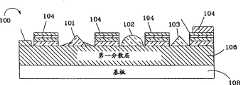
图9所示为一类似于图4及5中的发光二极管51的新的发光二极管100,但其在微发光二极管104之间具有LEEs 101、102、103。该些LEEs 101、102、103使被导向穿过一微发光二极管的侧面的光可从该LEEs反射出去,并将光从该基板重新导向到一外壳中。从基板108及第一分散层106之间的介面反射出去的光透过TIR还可以与LEEs 101、102、103相互作用而逸出到该外壳中以提供一较强的光输出。在图8中所述的LEEs可以沉积在新发光二极管上,或是加工到新发光二极管中。如上所述,LEE的厚度也可改变,较佳的厚度在0.5μm到10μm的范围内。Figure 9 shows a
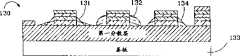
图10所示为一新发光二极管110,其类似于图9的发光二极管100,但其在该微发光二极管113之间具有随机的糙面的弥散LEE 112。光与粗糙层的相互作用使TIR光能以小于其临界角之下抵达表面,并且在被吸收之前逸出。在该较佳实施例中,通过使用聚苯乙烯或硅微球体作为一蚀刻掩模将微量粗糙度转到半导体中来形成该粗糙面。随机粗糙度的厚度及宽度可小于20nm,或多到500nm,较佳的尺寸大约为发光二极管所产生的光的波长。Figure 10 shows a
图11所示为一新发光二极管120,其类似于图10的发光二极管110,但其包括一在该微发光二极管中的电流阻隔层。该阻隔层122将电流导引到弥散LEE 124之下,增加了光与LEE相互作用及逸出的机会。Figure 11 shows a new LED 120, which is similar to
作为在微发光二极管之间形成LEEs的选择,可使LEEs直接形成于微发光二极管的侧面上。图12所示为一新发光二极管130,其类似于图9、10及11的发光二极管,但其具有直接形成于每个微发光二极管的侧面上的不同的LEEs 131-133。该LEEs可利用如上所述的相同的方法来形成。向微发光二极管侧面传播的光线被改向以使光线从基板134的其中一面通过第一分散层135或微发光二极管132逸出。由于在微发光二极管边上的该些LEEs,还使自基板134反射回来的光的逸出机会增加。As an alternative to forming LEEs between micro-LEDs, LEEs can be formed directly on the sides of the micro-LEDs. Figure 12 shows a
图13所示为一新发光二极管140,其有形成于微发光二极管144的侧面上的曲面的LEEs 142。该曲面LEE 142有额外的益处,其使发光二极管的光聚焦到一更明确的方向。LEEs 142的厚度及宽度可以随着任何一个LEE的较佳厚度而改变,该较佳厚度为0.1μm到50μm。FIG. 13 shows a
图14及15所示为两个额外的实施例。图14所示为一新发光二极管150,其在微发光二极管154的侧面上有一组合曲面的LEEs 152以及在该微发光二极管154之间有完全曲面的LEEs 156。该些LEEs共同作用,使光线折射及反射穿过基板逸出该发光二极管的外壳来加强光放出。Figures 14 and 15 show two additional embodiments. Figure 14 shows a new LED 150 with composite curved LEEs 152 on the sides of micro LEDs 154 and fully curved LEEs 156 between the micro LEDs 154. The LEEs work together to enhance light emission by refracting and reflecting light through the substrate and out of the LED housing.
图15所示为新的发光二极管160,其使用类似于图3所示的实施例的具体的倒装式安装。其在微发光二极管164的侧面上有曲面LEEs 162。该第二分散层164为反光的以及该基板166为主要的发射表面。LEEs 162及第二分散层164的部份共同作用,使光线折射及反射穿过基板逸出发光二极管的外壳来加强光放出。FIG. 15 shows a new LED 160 that uses a specific flip-chip mounting similar to the embodiment shown in FIG. 3 . It has curved LEEs 162 on the sides of micro LEDs 164. The second dispersion layer 164 is reflective and the substrate 166 is the main emitting surface. The LEEs 162 and portions of the second dispersion layer 164 work together to enhance light emission by refracting and reflecting light through the substrate and out of the LED housing.
虽然本发明已根据其若干较佳的配置作出了相当详细的叙述,其它的变型也是可能的。举例来说,在微发光二极管阵列中的微发光二极管的下层可以连接。所使用的光放出结构也可以作许多不同的组合以及有许多不同的形状及尺寸。同时,所述的发光二极管结构可具有多于一个夹在相反掺杂层之间的活性层。因此,本发明的权利要求书的精神及保护范围并不受限于其所述的较佳实施例。While the invention has been described in considerable detail in terms of several preferred configurations thereof, other variations are possible. For example, the lower layer of micro-LEDs in a micro-LED array can be connected. The light emitting structures used can also be used in many different combinations and in many different shapes and sizes. Also, the light emitting diode structure described can have more than one active layer sandwiched between oppositely doped layers. Therefore, the spirit and protection scope of the claims of the present invention are not limited to the preferred embodiments described therein.
Claims (10)
Applications Claiming Priority (4)
| Application Number | Priority Date | Filing Date | Title |
|---|---|---|---|
| US16881799P | 1999-12-03 | 1999-12-03 | |
| US60/168,817 | 1999-12-03 | ||
| US09/713,576 | 2000-11-14 | ||
| US09/713,576US6410942B1 (en) | 1999-12-03 | 2000-11-14 | Enhanced light extraction through the use of micro-LED arrays |
Publications (2)
| Publication Number | Publication Date |
|---|---|
| CN1402880A CN1402880A (en) | 2003-03-12 |
| CN1229871Ctrue CN1229871C (en) | 2005-11-30 |
Family
ID=26864480
Family Applications (1)
| Application Number | Title | Priority Date | Filing Date |
|---|---|---|---|
| CNB008166013AExpired - LifetimeCN1229871C (en) | 1999-12-03 | 2000-11-20 | Micro-LED arrays with enhanced light extraction |
Country Status (9)
| Country | Link |
|---|---|
| US (1) | US6410942B1 (en) |
| EP (3) | EP2325904B1 (en) |
| JP (1) | JP5511114B2 (en) |
| KR (1) | KR100731673B1 (en) |
| CN (1) | CN1229871C (en) |
| AU (1) | AU1790501A (en) |
| CA (1) | CA2393007C (en) |
| HK (1) | HK1048707A1 (en) |
| WO (1) | WO2001041219A1 (en) |
Cited By (1)
| Publication number | Priority date | Publication date | Assignee | Title |
|---|---|---|---|---|
| CN103312412A (en)* | 2012-03-06 | 2013-09-18 | 财团法人工业技术研究院 | Visible light communication transceiver and system |
Families Citing this family (367)
| Publication number | Priority date | Publication date | Assignee | Title |
|---|---|---|---|---|
| KR100700993B1 (en)* | 1999-12-03 | 2007-03-30 | 크리, 인코포레이티드 | Light emitting diode having improved light extraction structure and manufacturing method thereof |
| US7547921B2 (en)* | 2000-08-08 | 2009-06-16 | Osram Opto Semiconductors Gmbh | Semiconductor chip for optoelectronics |
| US20020017652A1 (en)* | 2000-08-08 | 2002-02-14 | Stefan Illek | Semiconductor chip for optoelectronics |
| JP2002141556A (en) | 2000-09-12 | 2002-05-17 | Lumileds Lighting Us Llc | Light-emitting diode with improved light extraction effect |
| US7053419B1 (en) | 2000-09-12 | 2006-05-30 | Lumileds Lighting U.S., Llc | Light emitting diodes with improved light extraction efficiency |
| US7064355B2 (en) | 2000-09-12 | 2006-06-20 | Lumileds Lighting U.S., Llc | Light emitting diodes with improved light extraction efficiency |
| JP2002198560A (en)* | 2000-12-26 | 2002-07-12 | Sharp Corp | Semiconductor light emitting device and method of manufacturing the same |
| US6791119B2 (en)* | 2001-02-01 | 2004-09-14 | Cree, Inc. | Light emitting diodes including modifications for light extraction |
| JP4724924B2 (en)* | 2001-02-08 | 2011-07-13 | ソニー株式会社 | Manufacturing method of display device |
| US6746889B1 (en)* | 2001-03-27 | 2004-06-08 | Emcore Corporation | Optoelectronic device with improved light extraction |
| US6987613B2 (en) | 2001-03-30 | 2006-01-17 | Lumileds Lighting U.S., Llc | Forming an optical element on the surface of a light emitting device for improved light extraction |
| JP2002344011A (en)* | 2001-05-15 | 2002-11-29 | Sony Corp | Display element and display device using the same |
| US6897704B2 (en)* | 2001-05-25 | 2005-05-24 | Thunder Creative Technologies, Inc. | Electronic isolator |
| TW583348B (en)* | 2001-06-19 | 2004-04-11 | Phoenix Prec Technology Corp | A method for electroplating Ni/Au layer substrate without using electroplating wire |
| JP4055503B2 (en)* | 2001-07-24 | 2008-03-05 | 日亜化学工業株式会社 | Semiconductor light emitting device |
| WO2003026355A2 (en)* | 2001-08-30 | 2003-03-27 | Osram Opto Semiconductors Gmbh | Electroluminescent body |
| TW523939B (en)* | 2001-11-07 | 2003-03-11 | Nat Univ Chung Hsing | High-efficient light emitting diode and its manufacturing method |
| US6881983B2 (en)* | 2002-02-25 | 2005-04-19 | Kopin Corporation | Efficient light emitting diodes and lasers |
| JP3776824B2 (en) | 2002-04-05 | 2006-05-17 | 株式会社東芝 | Semiconductor light emitting device and manufacturing method thereof |
| US20030189215A1 (en) | 2002-04-09 | 2003-10-09 | Jong-Lam Lee | Method of fabricating vertical structure leds |
| JP4585014B2 (en)* | 2002-04-12 | 2010-11-24 | ソウル セミコンダクター カンパニー リミテッド | Light emitting device |
| CN100552987C (en)* | 2002-05-28 | 2009-10-21 | 松下电工株式会社 | Light emitting device, lighting apparatus using the same, and surface light emitting lighting apparatus |
| US6841802B2 (en)* | 2002-06-26 | 2005-01-11 | Oriol, Inc. | Thin film light emitting diode |
| US6955985B2 (en)* | 2002-06-28 | 2005-10-18 | Kopin Corporation | Domain epitaxy for thin film growth |
| DE10234977A1 (en)* | 2002-07-31 | 2004-02-12 | Osram Opto Semiconductors Gmbh | Radiation-emitting thin layer semiconductor component comprises a multiple layer structure based on gallium nitride containing an active radiation-producing layer and having a first main surface and a second main surface |
| WO2004013916A1 (en)* | 2002-08-01 | 2004-02-12 | Nichia Corporation | Semiconductor light-emitting device, method for manufacturing same and light-emitting apparatus using same |
| KR20040013998A (en)* | 2002-08-09 | 2004-02-14 | 엘지전자 주식회사 | Fabrication method for led of limit exterior |
| ATE500616T1 (en)* | 2002-08-29 | 2011-03-15 | Seoul Semiconductor Co Ltd | LIGHT EMITTING COMPONENT WITH LIGHT EMITTING DIODES |
| JP3956918B2 (en) | 2002-10-03 | 2007-08-08 | 日亜化学工業株式会社 | Light emitting diode |
| US7071494B2 (en)* | 2002-12-11 | 2006-07-04 | Lumileds Lighting U.S. Llc | Light emitting device with enhanced optical scattering |
| EP1579511B1 (en)* | 2002-12-30 | 2012-03-28 | OSRAM Opto Semiconductors GmbH | Method for roughening a surface of an opto-electronic semiconductor body. |
| US7042020B2 (en)* | 2003-02-14 | 2006-05-09 | Cree, Inc. | Light emitting device incorporating a luminescent material |
| KR100964399B1 (en)* | 2003-03-08 | 2010-06-17 | 삼성전자주식회사 | Semiconductor laser diode and semiconductor laser diode assembly using same |
| US7211831B2 (en)* | 2003-04-15 | 2007-05-01 | Luminus Devices, Inc. | Light emitting device with patterned surfaces |
| US7105861B2 (en)* | 2003-04-15 | 2006-09-12 | Luminus Devices, Inc. | Electronic device contact structures |
| US7098589B2 (en) | 2003-04-15 | 2006-08-29 | Luminus Devices, Inc. | Light emitting devices with high light collimation |
| US7074631B2 (en)* | 2003-04-15 | 2006-07-11 | Luminus Devices, Inc. | Light emitting device methods |
| US6831302B2 (en)* | 2003-04-15 | 2004-12-14 | Luminus Devices, Inc. | Light emitting devices with improved extraction efficiency |
| US7521854B2 (en)* | 2003-04-15 | 2009-04-21 | Luminus Devices, Inc. | Patterned light emitting devices and extraction efficiencies related to the same |
| US7084434B2 (en)* | 2003-04-15 | 2006-08-01 | Luminus Devices, Inc. | Uniform color phosphor-coated light-emitting diode |
| US7166871B2 (en)* | 2003-04-15 | 2007-01-23 | Luminus Devices, Inc. | Light emitting systems |
| US7083993B2 (en) | 2003-04-15 | 2006-08-01 | Luminus Devices, Inc. | Methods of making multi-layer light emitting devices |
| US7274043B2 (en)* | 2003-04-15 | 2007-09-25 | Luminus Devices, Inc. | Light emitting diode systems |
| US7262550B2 (en)* | 2003-04-15 | 2007-08-28 | Luminus Devices, Inc. | Light emitting diode utilizing a physical pattern |
| US20040259279A1 (en)* | 2003-04-15 | 2004-12-23 | Erchak Alexei A. | Light emitting device methods |
| US7667238B2 (en)* | 2003-04-15 | 2010-02-23 | Luminus Devices, Inc. | Light emitting devices for liquid crystal displays |
| CA2523544A1 (en)* | 2003-04-30 | 2004-11-18 | Cree, Inc. | High powered light emitter packages with compact optics |
| US7005679B2 (en) | 2003-05-01 | 2006-02-28 | Cree, Inc. | Multiple component solid state white light |
| JP2006525669A (en) | 2003-05-02 | 2006-11-09 | ユニバーシティ・カレッジ・コークーナショナル・ユニバーシティ・オブ・アイルランド,コーク | Light emitting diode and manufacturing method thereof |
| US6885034B1 (en) | 2003-05-09 | 2005-04-26 | Winston Vaughan Schoenfeld | Light emitting diode having multiple pits |
| US7122841B2 (en) | 2003-06-04 | 2006-10-17 | Kopin Corporation | Bonding pad for gallium nitride-based light-emitting devices |
| US20050000913A1 (en)* | 2003-07-03 | 2005-01-06 | Mark Betterly | Fluid treatment system |
| US7009213B2 (en) | 2003-07-31 | 2006-03-07 | Lumileds Lighting U.S., Llc | Light emitting devices with improved light extraction efficiency |
| ES2356606T3 (en)* | 2003-08-08 | 2011-04-11 | Kang, Sang-Kyu | NITRIDE LIGHT EMITTER MICRODIODE WITH HIGH BRIGHTNESS AND MANUFACTURING PROCEDURE OF THE SAME. |
| WO2005018008A1 (en)* | 2003-08-19 | 2005-02-24 | Nichia Corporation | Semiconductor device |
| US7341880B2 (en)* | 2003-09-17 | 2008-03-11 | Luminus Devices, Inc. | Light emitting device processes |
| US7344903B2 (en)* | 2003-09-17 | 2008-03-18 | Luminus Devices, Inc. | Light emitting device processes |
| US7915085B2 (en) | 2003-09-18 | 2011-03-29 | Cree, Inc. | Molded chip fabrication method |
| JP4881003B2 (en)* | 2003-09-26 | 2012-02-22 | オスラム オプト セミコンダクターズ ゲゼルシャフト ミット ベシュレンクテル ハフツング | Thin film semiconductor chip that emits radiation |
| EP2320482B1 (en) | 2003-12-09 | 2016-11-16 | The Regents of The University of California | Highly efficient gallium nitride based light emitting diodes via surface roughening |
| US7450311B2 (en) | 2003-12-12 | 2008-11-11 | Luminus Devices, Inc. | Optical display systems and methods |
| JP2005191099A (en)* | 2003-12-24 | 2005-07-14 | ▲さん▼圓光電股▲ふん▼有限公司 | Light emitting diode device |
| US20050179042A1 (en)* | 2004-02-13 | 2005-08-18 | Kopin Corporation | Monolithic integration and enhanced light extraction in gallium nitride-based light-emitting devices |
| US20050179046A1 (en)* | 2004-02-13 | 2005-08-18 | Kopin Corporation | P-type electrodes in gallium nitride-based light-emitting devices |
| TWM271252U (en)* | 2004-12-14 | 2005-07-21 | Niching Ind Corp | Package structure of light-emitting device |
| JP2005259891A (en)* | 2004-03-10 | 2005-09-22 | Toyoda Gosei Co Ltd | Light emitting device |
| US7202141B2 (en)* | 2004-03-29 | 2007-04-10 | J.P. Sercel Associates, Inc. | Method of separating layers of material |
| US7419912B2 (en)* | 2004-04-01 | 2008-09-02 | Cree, Inc. | Laser patterning of light emitting devices |
| US7064356B2 (en)* | 2004-04-16 | 2006-06-20 | Gelcore, Llc | Flip chip light emitting diode with micromesas and a conductive mesh |
| US7795623B2 (en) | 2004-06-30 | 2010-09-14 | Cree, Inc. | Light emitting devices having current reducing structures and methods of forming light emitting devices having current reducing structures |
| US7534633B2 (en)* | 2004-07-02 | 2009-05-19 | Cree, Inc. | LED with substrate modifications for enhanced light extraction and method of making same |
| US20090023239A1 (en)* | 2004-07-22 | 2009-01-22 | Luminus Devices, Inc. | Light emitting device processes |
| US20060038188A1 (en)* | 2004-08-20 | 2006-02-23 | Erchak Alexei A | Light emitting diode systems |
| US20060049418A1 (en)* | 2004-09-03 | 2006-03-09 | Tzi-Chi Wen | Epitaxial structure and fabrication method of nitride semiconductor device |
| US7259402B2 (en)* | 2004-09-22 | 2007-08-21 | Cree, Inc. | High efficiency group III nitride-silicon carbide light emitting diode |
| US8513686B2 (en)* | 2004-09-22 | 2013-08-20 | Cree, Inc. | High output small area group III nitride LEDs |
| US7737459B2 (en)* | 2004-09-22 | 2010-06-15 | Cree, Inc. | High output group III nitride light emitting diodes |
| US8174037B2 (en)* | 2004-09-22 | 2012-05-08 | Cree, Inc. | High efficiency group III nitride LED with lenticular surface |
| US7352006B2 (en)* | 2004-09-28 | 2008-04-01 | Goldeneye, Inc. | Light emitting diodes exhibiting both high reflectivity and high light extraction |
| US7404756B2 (en) | 2004-10-29 | 2008-07-29 | 3M Innovative Properties Company | Process for manufacturing optical and semiconductor elements |
| US20060091411A1 (en) | 2004-10-29 | 2006-05-04 | Ouderkirk Andrew J | High brightness LED package |
| US7329982B2 (en) | 2004-10-29 | 2008-02-12 | 3M Innovative Properties Company | LED package with non-bonded optical element |
| US7462502B2 (en) | 2004-11-12 | 2008-12-09 | Philips Lumileds Lighting Company, Llc | Color control by alteration of wavelength converting element |
| US7419839B2 (en) | 2004-11-12 | 2008-09-02 | Philips Lumileds Lighting Company, Llc | Bonding an optical element to a light emitting device |
| JP2006147679A (en)* | 2004-11-17 | 2006-06-08 | Sony Corp | Integrated light emitting diode, manufacturing method of integrated light emitting diode, light emitting diode display, and light emitting diode illumination device |
| US7304363B1 (en) | 2004-11-26 | 2007-12-04 | United States Of America As Represented By The Secretary Of The Army | Interacting current spreader and junction extender to increase the voltage blocked in the off state of a high power semiconductor device |
| US20060124943A1 (en)* | 2004-12-14 | 2006-06-15 | Elite Optoelectronics Inc. | Large-sized light-emitting diodes with improved light extraction efficiency |
| US8288942B2 (en) | 2004-12-28 | 2012-10-16 | Cree, Inc. | High efficacy white LED |
| KR101138974B1 (en)* | 2005-01-07 | 2012-04-25 | 서울옵토디바이스주식회사 | Luminous element and method of manufacturing thereof |
| JP4687109B2 (en)* | 2005-01-07 | 2011-05-25 | ソニー株式会社 | Manufacturing method of integrated light emitting diode |
| US20060151801A1 (en)* | 2005-01-11 | 2006-07-13 | Doan Trung T | Light emitting diode with thermo-electric cooler |
| US7186580B2 (en)* | 2005-01-11 | 2007-03-06 | Semileds Corporation | Light emitting diodes (LEDs) with improved light extraction by roughening |
| US7524686B2 (en)* | 2005-01-11 | 2009-04-28 | Semileds Corporation | Method of making light emitting diodes (LEDs) with improved light extraction by roughening |
| US20060154393A1 (en)* | 2005-01-11 | 2006-07-13 | Doan Trung T | Systems and methods for removing operating heat from a light emitting diode |
| US7170100B2 (en) | 2005-01-21 | 2007-01-30 | Luminus Devices, Inc. | Packaging designs for LEDs |
| US7692207B2 (en)* | 2005-01-21 | 2010-04-06 | Luminus Devices, Inc. | Packaging designs for LEDs |
| US7335920B2 (en)* | 2005-01-24 | 2008-02-26 | Cree, Inc. | LED with current confinement structure and surface roughening |
| KR101138944B1 (en)* | 2005-01-26 | 2012-04-25 | 서울옵토디바이스주식회사 | Light emitting device having a plurality of light emitting cells connected in series and method of fabricating the same |
| US7535028B2 (en)* | 2005-02-03 | 2009-05-19 | Ac Led Lighting, L.Lc. | Micro-LED based high voltage AC/DC indicator lamp |
| JP2006261659A (en)* | 2005-02-18 | 2006-09-28 | Sumitomo Chemical Co Ltd | Manufacturing method of semiconductor light emitting device |
| US7932111B2 (en) | 2005-02-23 | 2011-04-26 | Cree, Inc. | Substrate removal process for high light extraction LEDs |
| US20060204865A1 (en)* | 2005-03-08 | 2006-09-14 | Luminus Devices, Inc. | Patterned light-emitting devices |
| US20070045640A1 (en)* | 2005-08-23 | 2007-03-01 | Erchak Alexei A | Light emitting devices for liquid crystal displays |
| US8163575B2 (en)* | 2005-06-17 | 2012-04-24 | Philips Lumileds Lighting Company Llc | Grown photonic crystals in semiconductor light emitting devices |
| KR100599012B1 (en) | 2005-06-29 | 2006-07-12 | 서울옵토디바이스주식회사 | Light Emitting Diode Having Thermally Conductive Substrate And Method Of Manufacturing The Same |
| US20090179211A1 (en)* | 2005-07-14 | 2009-07-16 | Tae-Kyung Yoo | Light emitting device |
| US20070018182A1 (en)* | 2005-07-20 | 2007-01-25 | Goldeneye, Inc. | Light emitting diodes with improved light extraction and reflectivity |
| US8674375B2 (en)* | 2005-07-21 | 2014-03-18 | Cree, Inc. | Roughened high refractive index layer/LED for high light extraction |
| US20070085098A1 (en)* | 2005-10-17 | 2007-04-19 | Luminus Devices, Inc. | Patterned devices and related methods |
| US7348603B2 (en)* | 2005-10-17 | 2008-03-25 | Luminus Devices, Inc. | Anisotropic collimation devices and related methods |
| US7388233B2 (en)* | 2005-10-17 | 2008-06-17 | Luminus Devices, Inc. | Patchwork patterned devices and related methods |
| US7391059B2 (en) | 2005-10-17 | 2008-06-24 | Luminus Devices, Inc. | Isotropic collimation devices and related methods |
| US20080099777A1 (en)* | 2005-10-19 | 2008-05-01 | Luminus Devices, Inc. | Light-emitting devices and related systems |
| KR100779078B1 (en)* | 2005-12-09 | 2007-11-27 | 한국전자통신연구원 | Silicon-based light emitting diode for enhancing light extraction efficiency and fabrication method thereof |
| JP4908837B2 (en)* | 2005-12-13 | 2012-04-04 | キヤノン株式会社 | Light emitting element array and image forming apparatus |
| CN101351891B (en) | 2005-12-22 | 2014-11-19 | 科锐公司 | lighting device |
| US7772604B2 (en) | 2006-01-05 | 2010-08-10 | Illumitex | Separate optical device for directing light from an LED |
| JP2007214260A (en)* | 2006-02-08 | 2007-08-23 | Matsushita Electric Ind Co Ltd | Semiconductor light emitting device and manufacturing method thereof |
| KR20070088145A (en)* | 2006-02-24 | 2007-08-29 | 엘지전자 주식회사 | Light emitting diodes and manufacturing method |
| US7525126B2 (en) | 2006-05-02 | 2009-04-28 | 3M Innovative Properties Company | LED package with converging optical element |
| US7390117B2 (en) | 2006-05-02 | 2008-06-24 | 3M Innovative Properties Company | LED package with compound converging optical element |
| JP2009538536A (en) | 2006-05-26 | 2009-11-05 | クリー エル イー ディー ライティング ソリューションズ インコーポレイテッド | Solid state light emitting device and method of manufacturing the same |
| WO2007142946A2 (en) | 2006-05-31 | 2007-12-13 | Cree Led Lighting Solutions, Inc. | Lighting device and method of lighting |
| KR100759896B1 (en)* | 2006-06-15 | 2007-09-18 | 삼성전자주식회사 | Backlight module equipped with at least one light emitting device and its manufacturing method |
| US7674639B2 (en)* | 2006-08-14 | 2010-03-09 | Bridgelux, Inc | GaN based LED with etched exposed surface for improved light extraction efficiency and method for making the same |
| EP2060155A2 (en)* | 2006-08-23 | 2009-05-20 | Cree Led Lighting Solutions, Inc. | Lighting device and lighting method |
| US20100224890A1 (en)* | 2006-09-18 | 2010-09-09 | Cree, Inc. | Light emitting diode chip with electrical insulation element |
| WO2008042351A2 (en) | 2006-10-02 | 2008-04-10 | Illumitex, Inc. | Led system and method |
| US20090275157A1 (en)* | 2006-10-02 | 2009-11-05 | Illumitex, Inc. | Optical device shaping |
| US20080087875A1 (en)* | 2006-10-11 | 2008-04-17 | Feng-Hsu Fan | Protection for the epitaxial structure of metal devices |
| US9318327B2 (en) | 2006-11-28 | 2016-04-19 | Cree, Inc. | Semiconductor devices having low threading dislocations and improved light extraction and methods of making the same |
| WO2008070604A1 (en)* | 2006-12-04 | 2008-06-12 | Cree Led Lighting Solutions, Inc. | Lighting device and lighting method |
| US9310026B2 (en) | 2006-12-04 | 2016-04-12 | Cree, Inc. | Lighting assembly and lighting method |
| US8110838B2 (en)* | 2006-12-08 | 2012-02-07 | Luminus Devices, Inc. | Spatial localization of light-generating portions in LEDs |
| EP2111640B1 (en)* | 2007-01-22 | 2019-05-08 | Cree, Inc. | Fault tolerant light emitter and method of fabricating the same |
| TWI440210B (en) | 2007-01-22 | 2014-06-01 | Cree Inc | Illumination device using external interconnection array of light-emitting device and manufacturing method thereof |
| US8110425B2 (en) | 2007-03-20 | 2012-02-07 | Luminus Devices, Inc. | Laser liftoff structure and related methods |
| KR100849826B1 (en) | 2007-03-29 | 2008-07-31 | 삼성전기주식회사 | Light emitting device and package containing same |
| WO2009012287A1 (en)* | 2007-07-17 | 2009-01-22 | Cree Led Lighting Solutions, Inc. | Optical elements with internal optical features and methods of fabricating same |
| US8617997B2 (en)* | 2007-08-21 | 2013-12-31 | Cree, Inc. | Selective wet etching of gold-tin based solder |
| US11114594B2 (en)* | 2007-08-24 | 2021-09-07 | Creeled, Inc. | Light emitting device packages using light scattering particles of different size |
| US8368100B2 (en)* | 2007-11-14 | 2013-02-05 | Cree, Inc. | Semiconductor light emitting diodes having reflective structures and methods of fabricating same |
| US9431589B2 (en)* | 2007-12-14 | 2016-08-30 | Cree, Inc. | Textured encapsulant surface in LED packages |
| DE102008019902A1 (en)* | 2007-12-21 | 2009-06-25 | Osram Opto Semiconductors Gmbh | Optoelectronic component and production method for an optoelectronic component |
| DE102008003182A1 (en)* | 2008-01-04 | 2009-07-09 | Osram Opto Semiconductors Gmbh | Optoelectronic component |
| JP2011512037A (en) | 2008-02-08 | 2011-04-14 | イルミテックス, インコーポレイテッド | System and method for emitter layer shaping |
| JP5094535B2 (en)* | 2008-05-07 | 2012-12-12 | 富士フイルム株式会社 | Recess formation method, uneven product manufacturing method, light emitting element manufacturing method, and optical element manufacturing method |
| CA2732795C (en)* | 2008-06-11 | 2016-08-09 | Susanne Gardner | Beverages composed of wine components |
| US7939839B2 (en)* | 2008-09-11 | 2011-05-10 | Bridgelux, Inc. | Series connected segmented LED |
| US7825427B2 (en)* | 2008-09-12 | 2010-11-02 | Bridgelux, Inc. | Method and apparatus for generating phosphor film with textured surface |
| US9051177B2 (en)* | 2008-10-27 | 2015-06-09 | The United States Of America As Represented By The Secretary Of The Army | Active optical limiting semiconductor device and method with active region transparent to light becoming opaque when not biased |
| TWI375338B (en)* | 2008-11-27 | 2012-10-21 | Epistar Corp | Opto-electronic device |
| TW201034256A (en) | 2008-12-11 | 2010-09-16 | Illumitex Inc | Systems and methods for packaging light-emitting diode devices |
| TWI418060B (en)* | 2008-12-26 | 2013-12-01 | Lextar Electronics Corp | Method for manufacturing light-emitting diode wafer |
| US7982409B2 (en)* | 2009-02-26 | 2011-07-19 | Bridgelux, Inc. | Light sources utilizing segmented LEDs to compensate for manufacturing variations in the light output of individual segmented LEDs |
| KR101134810B1 (en) | 2009-03-03 | 2012-04-13 | 엘지이노텍 주식회사 | Light emitting device and method for fabricating the same |
| JP5196403B2 (en)* | 2009-03-23 | 2013-05-15 | 国立大学法人山口大学 | Method for manufacturing sapphire substrate and semiconductor device |
| US8585253B2 (en) | 2009-08-20 | 2013-11-19 | Illumitex, Inc. | System and method for color mixing lens array |
| US8449128B2 (en) | 2009-08-20 | 2013-05-28 | Illumitex, Inc. | System and method for a lens and phosphor layer |
| KR101039931B1 (en)* | 2009-10-21 | 2011-06-09 | 엘지이노텍 주식회사 | Light emitting device and manufacturing method |
| KR20110043282A (en)* | 2009-10-21 | 2011-04-27 | 엘지이노텍 주식회사 | Light emitting device and manufacturing method |
| US8783915B2 (en) | 2010-02-11 | 2014-07-22 | Bridgelux, Inc. | Surface-textured encapsulations for use with light emitting diodes |
| KR100999733B1 (en)* | 2010-02-18 | 2010-12-08 | 엘지이노텍 주식회사 | Light emitting device, light emitting device manufacturing method and light emitting device package |
| US8338317B2 (en) | 2011-04-06 | 2012-12-25 | Infineon Technologies Ag | Method for processing a semiconductor wafer or die, and particle deposition device |
| KR101601624B1 (en)* | 2010-02-19 | 2016-03-09 | 삼성전자주식회사 | Semiconductor light emitting device having a multi-cell array, light emitting module and illumination apparatus |
| TWI485884B (en)* | 2010-03-30 | 2015-05-21 | Advanced Optoelectronic Tech | Light-emitting diode and method for manufacturing the same |
| US8329482B2 (en) | 2010-04-30 | 2012-12-11 | Cree, Inc. | White-emitting LED chips and method for making same |
| KR20110132136A (en)* | 2010-06-01 | 2011-12-07 | 삼성전자주식회사 | Light emitting device using connection structure and manufacturing method thereof |
| US8193546B2 (en)* | 2010-06-04 | 2012-06-05 | Pinecone Energies, Inc. | Light-emitting-diode array with polymer between light emitting devices |
| KR20130046434A (en)* | 2010-07-26 | 2013-05-07 | 가부시키가이샤 한도오따이 에네루기 켄큐쇼 | Light emitting device and lighting device |
| US9070851B2 (en) | 2010-09-24 | 2015-06-30 | Seoul Semiconductor Co., Ltd. | Wafer-level light emitting diode package and method of fabricating the same |
| US9899329B2 (en) | 2010-11-23 | 2018-02-20 | X-Celeprint Limited | Interconnection structures and methods for transfer-printed integrated circuit elements with improved interconnection alignment tolerance |
| JP5589812B2 (en) | 2010-12-06 | 2014-09-17 | 豊田合成株式会社 | Semiconductor light emitting device |
| US9166126B2 (en) | 2011-01-31 | 2015-10-20 | Cree, Inc. | Conformally coated light emitting devices and methods for providing the same |
| TWI467805B (en)* | 2011-03-08 | 2015-01-01 | Opto Tech Corp | Light-emitting diode with wide viewing angle and manufacturing method thereof |
| KR101115538B1 (en)* | 2011-04-04 | 2012-02-28 | 서울옵토디바이스주식회사 | Luminous device and the method therefor |
| KR101106139B1 (en)* | 2011-04-04 | 2012-01-20 | 서울옵토디바이스주식회사 | Flip bonded light emitting diode having an extended metal reflective layer and a method of manufacturing the same |
| US20120261686A1 (en)* | 2011-04-12 | 2012-10-18 | Lu Chi Wei | Light-emitting element and the manufacturing method thereof |
| KR101737981B1 (en) | 2011-05-17 | 2017-05-22 | 한국전자통신연구원 | GAlIUM-NITRIDE LIGHT EMITTING DEVICE OF MICROARRAY TYPE STRUCTURE AND MANUFACTURING THEREOF |
| US8889485B2 (en) | 2011-06-08 | 2014-11-18 | Semprius, Inc. | Methods for surface attachment of flipped active componenets |
| KR101221336B1 (en)* | 2011-07-12 | 2013-01-21 | 서울옵토디바이스주식회사 | Light emitting device and method of fabricating the same |
| US8957440B2 (en) | 2011-10-04 | 2015-02-17 | Cree, Inc. | Light emitting devices with low packaging factor |
| KR101901589B1 (en)* | 2011-11-14 | 2018-09-27 | 엘지이노텍 주식회사 | Light emitting device |
| US8573469B2 (en) | 2011-11-18 | 2013-11-05 | LuxVue Technology Corporation | Method of forming a micro LED structure and array of micro LED structures with an electrically insulating layer |
| US8794501B2 (en) | 2011-11-18 | 2014-08-05 | LuxVue Technology Corporation | Method of transferring a light emitting diode |
| US8349116B1 (en) | 2011-11-18 | 2013-01-08 | LuxVue Technology Corporation | Micro device transfer head heater assembly and method of transferring a micro device |
| US8333860B1 (en) | 2011-11-18 | 2012-12-18 | LuxVue Technology Corporation | Method of transferring a micro device |
| KR101337613B1 (en)* | 2011-12-06 | 2013-12-06 | 서울바이오시스 주식회사 | Luminous device and the method therefor |
| CN104081523A (en) | 2012-02-02 | 2014-10-01 | 宝洁公司 | Light emitting laminate and method of making thereof |
| US9472594B2 (en)* | 2012-02-10 | 2016-10-18 | Oculus Vr, Llc | Light emitting diode chip |
| GB201215632D0 (en) | 2012-09-03 | 2012-10-17 | Infiniled Ltd | Optical device |
| JP5462333B1 (en) | 2012-09-21 | 2014-04-02 | 株式会社東芝 | Semiconductor light emitting device and manufacturing method thereof |
| DE102012109460B4 (en)* | 2012-10-04 | 2024-03-07 | OSRAM Opto Semiconductors Gesellschaft mit beschränkter Haftung | Method for producing a light-emitting diode display and light-emitting diode display |
| US9279947B2 (en)* | 2012-11-15 | 2016-03-08 | 4233999 Canada Inc. | Methods and apparatus for high speed short distance optical communications using micro light emitting diodes |
| US8558254B1 (en) | 2012-11-29 | 2013-10-15 | Hong Kong Applied Science and Technology Research Institute Company Limited | High reliability high voltage vertical LED arrays |
| US9105714B2 (en)* | 2012-12-11 | 2015-08-11 | LuxVue Technology Corporation | Stabilization structure including sacrificial release layer and staging bollards |
| US9166114B2 (en)* | 2012-12-11 | 2015-10-20 | LuxVue Technology Corporation | Stabilization structure including sacrificial release layer and staging cavity |
| US9306138B2 (en)* | 2013-04-08 | 2016-04-05 | Xiamen Sanan Optoelectronics Technology Co., Ltd. | Light emitting diode packaging structure |
| EP3008553B1 (en) | 2013-06-12 | 2023-06-07 | Rohinni, Inc. | Keyboard backlighting with deposited light-generating sources |
| CN104241262B (en) | 2013-06-14 | 2020-11-06 | 惠州科锐半导体照明有限公司 | Light emitting device and display device |
| DE102013107967B4 (en)* | 2013-07-25 | 2021-05-06 | OSRAM Opto Semiconductors Gesellschaft mit beschränkter Haftung | Optoelectronic semiconductor chip, optoelectronic component and method for producing a plurality of optoelectronic semiconductor chips |
| JP2014064012A (en)* | 2013-10-28 | 2014-04-10 | Toshiba Corp | Semiconductor light-emitting element and method of manufacturing the same |
| JP6684541B2 (en)* | 2014-01-20 | 2020-04-22 | ローム株式会社 | Light emitting element |
| DE102014009677A1 (en)* | 2014-02-19 | 2015-08-20 | Pierre-Alain Cotte | Display device with improved contrast |
| US9105813B1 (en)* | 2014-05-30 | 2015-08-11 | Mikro Mesa Technology Co., Ltd. | Micro-light-emitting diode |
| US9231153B2 (en)* | 2014-05-30 | 2016-01-05 | Mikro Mesa Technology Co., Ltd. | Micro-light-emitting diode |
| US9444015B2 (en) | 2014-06-18 | 2016-09-13 | X-Celeprint Limited | Micro assembled LED displays and lighting elements |
| WO2016030422A1 (en) | 2014-08-26 | 2016-03-03 | X-Celeprint Limited | Micro assembled hybrid displays and lighting elements |
| US9991163B2 (en) | 2014-09-25 | 2018-06-05 | X-Celeprint Limited | Small-aperture-ratio display with electrical component |
| US9799719B2 (en) | 2014-09-25 | 2017-10-24 | X-Celeprint Limited | Active-matrix touchscreen |
| US9799261B2 (en) | 2014-09-25 | 2017-10-24 | X-Celeprint Limited | Self-compensating circuit for faulty display pixels |
| US9818725B2 (en) | 2015-06-01 | 2017-11-14 | X-Celeprint Limited | Inorganic-light-emitter display with integrated black matrix |
| US9433050B2 (en)* | 2014-10-08 | 2016-08-30 | Mikro Mesa Technology Co., Ltd. | Micro-light-emitting diode |
| US10516084B2 (en) | 2014-10-31 | 2019-12-24 | eLux, Inc. | Encapsulated fluid assembly emissive elements |
| US12119432B2 (en)* | 2014-10-31 | 2024-10-15 | eLux, Inc. | Encapsulated light emitting diodes for selective fluidic assembly |
| GB201420452D0 (en)* | 2014-11-18 | 2014-12-31 | Mled Ltd | Integrated colour led micro-display |
| USD826871S1 (en) | 2014-12-11 | 2018-08-28 | Cree, Inc. | Light emitting diode device |
| KR102175991B1 (en) | 2014-12-26 | 2020-11-09 | 삼성디스플레이 주식회사 | Display apparatus and manufacturing method thereof |
| KR102347533B1 (en)* | 2014-12-26 | 2022-01-05 | 삼성디스플레이 주식회사 | Display apparatus and manufacturing method thereof |
| TWI610459B (en)* | 2015-05-13 | 2018-01-01 | 友達光電股份有限公司 | Miniature light emitting diode device and manufacturing method thereof |
| US9871345B2 (en) | 2015-06-09 | 2018-01-16 | X-Celeprint Limited | Crystalline color-conversion device |
| CN106299095A (en)* | 2015-06-12 | 2017-01-04 | 映瑞光电科技(上海)有限公司 | A kind of high pressure flip LED chips and preparation method thereof |
| US10133426B2 (en) | 2015-06-18 | 2018-11-20 | X-Celeprint Limited | Display with micro-LED front light |
| US11061276B2 (en) | 2015-06-18 | 2021-07-13 | X Display Company Technology Limited | Laser array display |
| US10255834B2 (en) | 2015-07-23 | 2019-04-09 | X-Celeprint Limited | Parallel redundant chiplet system for controlling display pixels |
| US10380930B2 (en) | 2015-08-24 | 2019-08-13 | X-Celeprint Limited | Heterogeneous light emitter display system |
| KR102393374B1 (en) | 2015-08-31 | 2022-05-03 | 삼성디스플레이 주식회사 | Display apparatus and method of manufacturing the same |
| KR102424975B1 (en)* | 2015-08-31 | 2022-07-26 | 삼성디스플레이 주식회사 | Light emitting diode structure and display apparatus |
| USD777972S1 (en) | 2015-09-03 | 2017-01-31 | Svv Technology Innovations, Inc. | Light emitting sheet with surface pattern |
| USD803472S1 (en) | 2015-09-03 | 2017-11-21 | Svv Technology Innovations, Inc. | Light emitting sheet with surface pattern |
| USD829969S1 (en) | 2015-09-03 | 2018-10-02 | Svv Technology Innovations, Inc. | Light emitting sheet with surface pattern |
| USD799738S1 (en) | 2015-09-03 | 2017-10-10 | Svv Technology Innovations, Inc. | LED lighting sheet with surface pattern |
| US10230048B2 (en) | 2015-09-29 | 2019-03-12 | X-Celeprint Limited | OLEDs for micro transfer printing |
| TWI576007B (en) | 2015-11-23 | 2017-03-21 | 財團法人工業技術研究院 | Driving method of light emitting device and light emitting device |
| US10066819B2 (en) | 2015-12-09 | 2018-09-04 | X-Celeprint Limited | Micro-light-emitting diode backlight system |
| US9747503B2 (en) | 2015-12-30 | 2017-08-29 | Surefire Llc | Optical narrowcasting augmented reality |
| JP6959697B2 (en) | 2016-01-15 | 2021-11-05 | ロヒンニ リミテッド ライアビリティ カンパニー | Devices and methods that are backlit through a cover on the device |
| TWI710061B (en) | 2016-02-25 | 2020-11-11 | 愛爾蘭商艾克斯展示公司技術有限公司 | Efficiently micro-transfer printing micro-scale devices onto large-format substrates |
| US10193025B2 (en) | 2016-02-29 | 2019-01-29 | X-Celeprint Limited | Inorganic LED pixel structure |
| US10153257B2 (en) | 2016-03-03 | 2018-12-11 | X-Celeprint Limited | Micro-printed display |
| US10153256B2 (en) | 2016-03-03 | 2018-12-11 | X-Celeprint Limited | Micro-transfer printable electronic component |
| CN205944139U (en) | 2016-03-30 | 2017-02-08 | 首尔伟傲世有限公司 | Ultraviolet ray light -emitting diode spare and contain this emitting diode module |
| US10008483B2 (en) | 2016-04-05 | 2018-06-26 | X-Celeprint Limited | Micro-transfer printed LED and color filter structure |
| US10199546B2 (en) | 2016-04-05 | 2019-02-05 | X-Celeprint Limited | Color-filter device |
| NL2016716B1 (en) | 2016-05-02 | 2017-11-10 | Nts Systems Dev B V | Exposure system, printing system, method for additive manufacturing, a composition, and the use thereof. |
| US9997501B2 (en) | 2016-06-01 | 2018-06-12 | X-Celeprint Limited | Micro-transfer-printed light-emitting diode device |
| US11137641B2 (en) | 2016-06-10 | 2021-10-05 | X Display Company Technology Limited | LED structure with polarized light emission |
| KR102608419B1 (en)* | 2016-07-12 | 2023-12-01 | 삼성디스플레이 주식회사 | Display Apparatus and Method for manufacturing the same |
| DE102016112972A1 (en)* | 2016-07-14 | 2018-01-18 | Osram Opto Semiconductors Gmbh | Optoelectronic semiconductor chip |
| US9980341B2 (en) | 2016-09-22 | 2018-05-22 | X-Celeprint Limited | Multi-LED components |
| US10782002B2 (en) | 2016-10-28 | 2020-09-22 | X Display Company Technology Limited | LED optical components |
| US10347168B2 (en) | 2016-11-10 | 2019-07-09 | X-Celeprint Limited | Spatially dithered high-resolution |
| US10600671B2 (en) | 2016-11-15 | 2020-03-24 | X-Celeprint Limited | Micro-transfer-printable flip-chip structures and methods |
| US10395966B2 (en) | 2016-11-15 | 2019-08-27 | X-Celeprint Limited | Micro-transfer-printable flip-chip structures and methods |
| EP3542394B1 (en) | 2016-11-15 | 2025-09-24 | X Display Company Technology Limited | Micro-transfer-printable flip-chip structures and manufacturing methods thereof |
| US10193018B2 (en)* | 2016-12-29 | 2019-01-29 | Intel Corporation | Compact low power head-mounted display with light emitting diodes that exhibit a desired beam angle |
| CN109564963B (en) | 2017-01-26 | 2021-04-16 | 株式会社Lg化学 | Micro LED and display device including the same |
| CN106935608B (en)* | 2017-02-27 | 2019-10-25 | 深圳市华星光电技术有限公司 | Micro-LED array substrate and display panel |
| US11024608B2 (en) | 2017-03-28 | 2021-06-01 | X Display Company Technology Limited | Structures and methods for electrical connection of micro-devices and substrates |
| US9917652B1 (en) | 2017-06-06 | 2018-03-13 | Surefire Llc | Adaptive communications focal plane array |
| DE102017114369A1 (en)* | 2017-06-28 | 2019-01-03 | Osram Opto Semiconductors Gmbh | Optoelectronic component |
| KR102418952B1 (en) | 2017-08-31 | 2022-07-08 | 삼성전자주식회사 | Home appliance having voice recognizing function |
| WO2019051764A1 (en)* | 2017-09-15 | 2019-03-21 | 厦门市三安光电科技有限公司 | Microscopic light-emitting diode, and manufacturing method therefor |
| US10020422B1 (en)* | 2017-09-29 | 2018-07-10 | Oculus Vr, Llc | Mesa shaped micro light emitting diode with bottom N-contact |
| EP3462489B1 (en)* | 2017-09-29 | 2021-05-26 | Facebook Technologies, LLC | Mesa shaped micro light emitting diode with bottom n-contact |
| TWI641778B (en) | 2017-12-19 | 2018-11-21 | 宏碁股份有限公司 | Miniaturized light-emitting device |
| US20190198564A1 (en)* | 2017-12-20 | 2019-06-27 | Lumileds Llc | Monolithic segmented led array architecture with islanded epitaxial growth |
| KR102428029B1 (en) | 2017-12-20 | 2022-08-02 | (주)포인트엔지니어링 | Trnasfer head for micro led |
| US11961875B2 (en) | 2017-12-20 | 2024-04-16 | Lumileds Llc | Monolithic segmented LED array architecture with islanded epitaxial growth |
| US11355548B2 (en) | 2017-12-20 | 2022-06-07 | Lumileds Llc | Monolithic segmented LED array architecture |
| US11749790B2 (en) | 2017-12-20 | 2023-09-05 | Lumileds Llc | Segmented LED with embedded transistors |
| US11296262B2 (en) | 2017-12-21 | 2022-04-05 | Lumileds Llc | Monolithic segmented LED array architecture with reduced area phosphor emission surface |
| US10957820B2 (en) | 2017-12-21 | 2021-03-23 | Lumileds Llc | Monolithic, segmented light emitting diode array |
| US10879431B2 (en) | 2017-12-22 | 2020-12-29 | Lumileds Llc | Wavelength converting layer patterning for LED arrays |
| US10418510B1 (en) | 2017-12-22 | 2019-09-17 | Facebook Technologies, Llc | Mesa shaped micro light emitting diode with electroless plated N-contact |
| US10250948B1 (en) | 2018-01-05 | 2019-04-02 | Aron Surefire, Llc | Social media with optical narrowcasting |
| US10473439B2 (en) | 2018-01-05 | 2019-11-12 | Aron Surefire, Llc | Gaming systems and methods using optical narrowcasting |
| US10236986B1 (en) | 2018-01-05 | 2019-03-19 | Aron Surefire, Llc | Systems and methods for tiling free space optical transmissions |
| KR102536305B1 (en) | 2018-01-05 | 2023-05-24 | (주)포인트엔지니어링 | Micro led structure and manufactureing method of the same |
| CN110323248B (en)* | 2018-03-28 | 2021-09-14 | 英属开曼群岛商镎创科技股份有限公司 | Light emitting diode display panel and manufacturing method thereof |
| KR20190114333A (en) | 2018-03-29 | 2019-10-10 | (주)포인트엔지니어링 | Inspection method for micro led |
| KR20190114334A (en) | 2018-03-29 | 2019-10-10 | (주)포인트엔지니어링 | Inspection and repair method for micro led |
| KR20190114330A (en) | 2018-03-29 | 2019-10-10 | (주)포인트엔지니어링 | Transfer head for micro led |
| KR20190114372A (en) | 2018-03-30 | 2019-10-10 | (주)포인트엔지니어링 | Transfer system for micro led |
| KR20190114368A (en) | 2018-03-30 | 2019-10-10 | (주)포인트엔지니어링 | Micro led semi-product module |
| KR102481434B1 (en) | 2018-03-30 | 2022-12-26 | (주)포인트엔지니어링 | Transfer head and adsorbing method for micro led using the same |
| KR102424246B1 (en) | 2018-03-30 | 2022-07-25 | (주)포인트엔지니어링 | Transfer system for micro led with transfer head |
| KR102471585B1 (en) | 2018-04-06 | 2022-11-28 | (주)포인트엔지니어링 | Micro led adsorption body and micro led inspection system using the same |
| KR20190117180A (en) | 2018-04-06 | 2019-10-16 | (주)포인트엔지니어링 | Micro led adsorption body and micro led inspection system using the same |
| KR102498037B1 (en) | 2018-04-20 | 2023-02-10 | (주)포인트엔지니어링 | Micro led adsorption body |
| TW201944086A (en) | 2018-04-06 | 2019-11-16 | 南韓商普因特工程有限公司 | Micro LED adsorption body |
| KR20190120598A (en) | 2018-04-16 | 2019-10-24 | (주)포인트엔지니어링 | Micro led transfer system including micro led adsorption body |
| KR102471583B1 (en) | 2018-04-16 | 2022-11-28 | (주)포인트엔지니어링 | Micro led transfer system including micro led adsorption body |
| KR102498109B1 (en) | 2018-04-20 | 2023-02-09 | (주)포인트엔지니어링 | Micro led transfer system |
| KR102498112B1 (en) | 2018-04-27 | 2023-02-09 | (주)포인트엔지니어링 | Micro led transfer head |
| KR20190124920A (en) | 2018-04-27 | 2019-11-06 | (주)포인트엔지니어링 | Device transfer head |
| KR102527138B1 (en) | 2018-05-16 | 2023-04-28 | (주)포인트엔지니어링 | Micro led transfer system |
| KR20190131311A (en) | 2018-05-16 | 2019-11-26 | (주)포인트엔지니어링 | Micro led adsorption body |
| KR102517784B1 (en) | 2018-05-16 | 2023-04-04 | (주)포인트엔지니어링 | Micro led adsorption body |
| KR102457191B1 (en) | 2018-05-16 | 2022-10-20 | (주)포인트엔지니어링 | Micro led transfer system |
| KR102540860B1 (en) | 2018-05-29 | 2023-06-07 | (주)포인트엔지니어링 | Transfer head for micro led and micro led transfer system using the same |
| KR102540859B1 (en) | 2018-05-29 | 2023-06-07 | (주)포인트엔지니어링 | Transfer head for micro led and micro led transfer system using the same |
| CN110544661A (en)* | 2018-05-29 | 2019-12-06 | 普因特工程有限公司 | Micro LED transfer printing head and micro LED transfer printing system using it |
| KR20190135862A (en) | 2018-05-29 | 2019-12-09 | (주)포인트엔지니어링 | Micro led transfer system |
| KR102457193B1 (en) | 2018-05-29 | 2022-10-20 | (주)포인트엔지니어링 | Micro led adsorption body |
| KR20190136562A (en) | 2018-05-31 | 2019-12-10 | (주)포인트엔지니어링 | Transfer head for micro led |
| KR102527139B1 (en) | 2018-06-15 | 2023-04-28 | (주)포인트엔지니어링 | Transfer head for micro led and transfer stage for micro led |
| KR102643764B1 (en) | 2018-06-27 | 2024-03-06 | (주)포인트엔지니어링 | Transfer head for micro led |
| KR102541195B1 (en) | 2018-06-27 | 2023-06-09 | (주)포인트엔지니어링 | Transfer head for micro led |
| CN110648956A (en) | 2018-06-27 | 2020-01-03 | 普因特工程有限公司 | Micro light emitting diode transfer head |
| KR20200005237A (en) | 2018-07-06 | 2020-01-15 | (주)포인트엔지니어링 | Micro led transfer head and micro led transfer system using the same |
| KR20200005234A (en) | 2018-07-06 | 2020-01-15 | (주)포인트엔지니어링 | Transfer head for micro led |
| KR20200005235A (en) | 2018-07-06 | 2020-01-15 | (주)포인트엔지니어링 | Transfer head for micro led |
| KR20200015073A (en) | 2018-08-02 | 2020-02-12 | (주)포인트엔지니어링 | Micro led transfer system |
| KR20200015082A (en) | 2018-08-02 | 2020-02-12 | (주)포인트엔지니어링 | Micro led structure and manufacturing method of the same |
| KR20200015081A (en) | 2018-08-02 | 2020-02-12 | (주)포인트엔지니어링 | Micro led transfer head |
| KR20200015071A (en) | 2018-08-02 | 2020-02-12 | (주)포인트엔지니어링 | Transfer head for micro led |
| KR20200015076A (en) | 2018-08-02 | 2020-02-12 | (주)포인트엔지니어링 | Hot air supplying head for transfering micro led and micro led transfer system using the same |
| JP7398818B2 (en) | 2018-08-10 | 2023-12-15 | ビジョンラボ コーポレーション | Fluid transfer system and method for manufacturing micro LED device |
| KR20200020207A (en) | 2018-08-16 | 2020-02-26 | (주)포인트엔지니어링 | Transfer head for micro led |
| KR20200020208A (en) | 2018-08-16 | 2020-02-26 | (주)포인트엔지니어링 | Micro led transfer system |
| KR20200025079A (en) | 2018-08-29 | 2020-03-10 | (주)포인트엔지니어링 | Transfer head |
| US10811460B2 (en) | 2018-09-27 | 2020-10-20 | Lumileds Holding B.V. | Micrometer scale light emitting diode displays on patterned templates and substrates |
| US10964845B2 (en) | 2018-09-27 | 2021-03-30 | Lumileds Llc | Micro light emitting devices |
| US11201265B2 (en) | 2018-09-27 | 2021-12-14 | Lumileds Llc | Micro light emitting devices |
| US10923628B2 (en) | 2018-09-27 | 2021-02-16 | Lumileds Llc | Micrometer scale light emitting diode displays on patterned templates and substrates |
| KR20200053841A (en) | 2018-11-09 | 2020-05-19 | (주)포인트엔지니어링 | Micro led carrier for correcting position error and micro led transfer system |
| KR20200085507A (en) | 2019-01-07 | 2020-07-15 | (주)포인트엔지니어링 | Transfer head for micro led |
| KR20200095909A (en) | 2019-02-01 | 2020-08-11 | (주)포인트엔지니어링 | Transfer head for micro led |
| KR20200099019A (en) | 2019-02-13 | 2020-08-21 | (주)포인트엔지니어링 | Micro led adsorption body |
| KR20200129751A (en) | 2019-05-10 | 2020-11-18 | (주)포인트엔지니어링 | Micro led adsorption body and manufacturing method of micro led display using the same and micro led display |
| KR20200135069A (en) | 2019-05-24 | 2020-12-02 | (주)포인트엔지니어링 | Micro led display manufacturing and micro led display using the same |
| KR102723703B1 (en)* | 2019-05-28 | 2024-10-31 | 삼성디스플레이 주식회사 | Display device and manufacturing method for display device |
| KR102705311B1 (en)* | 2019-06-13 | 2024-09-10 | 엘지전자 주식회사 | Lighting device using micro-led and manufacturing method thereof |
| KR102708645B1 (en) | 2019-07-08 | 2024-09-24 | (주)포인트엔지니어링 | Micro led group plate and manufacturing method thereof and micro led display panel and manufacturing method thereof |
| US11152534B2 (en) | 2019-08-07 | 2021-10-19 | Point Engineering Co., Ltd. | Transfer head and method of manufacturing micro LED display using same |
| KR20210020433A (en) | 2019-08-14 | 2021-02-24 | (주)포인트엔지니어링 | Micro led display manufacturing |
| KR102819268B1 (en) | 2019-08-14 | 2025-06-11 | (주)포인트엔지니어링 | Transfer head for micro led |
| KR20210020421A (en) | 2019-08-14 | 2021-02-24 | (주)포인트엔지니어링 | Manufacturing method of micro device display |
| KR20210025217A (en) | 2019-08-27 | 2021-03-09 | (주)포인트엔지니어링 | Micro led transfer head and manufacturing method of micro led display using the same |
| KR20210025216A (en) | 2019-08-27 | 2021-03-09 | (주)포인트엔지니어링 | Micro led repair device and manufacturing of micor led display using the same |
| WO2021086935A1 (en)* | 2019-10-28 | 2021-05-06 | The Regents Of The University Of California | Formation of microled mesa structures with atomic layer deposition passivated sidewalls, a self-aligned dielectric via to the top electrical contact, and a plasma-damage-free top contact |
| KR20210063671A (en) | 2019-11-25 | 2021-06-02 | (주)포인트엔지니어링 | Micro led display manufacturing |
| US20220416119A1 (en)* | 2019-12-03 | 2022-12-29 | Vuereal Inc. | High efficient micro devices |
| US11674795B2 (en) | 2019-12-18 | 2023-06-13 | Lumileds Llc | Miniature pattern projector using microLEDs and micro-optics |
| US11923398B2 (en) | 2019-12-23 | 2024-03-05 | Lumileds Llc | III-nitride multi-wavelength LED arrays |
| US11404473B2 (en) | 2019-12-23 | 2022-08-02 | Lumileds Llc | III-nitride multi-wavelength LED arrays |
| KR102168570B1 (en) | 2020-03-03 | 2020-10-21 | 오재열 | Micro LED Transfer Board |
| US11569415B2 (en) | 2020-03-11 | 2023-01-31 | Lumileds Llc | Light emitting diode devices with defined hard mask opening |
| US11848402B2 (en) | 2020-03-11 | 2023-12-19 | Lumileds Llc | Light emitting diode devices with multilayer composite film including current spreading layer |
| US11735695B2 (en) | 2020-03-11 | 2023-08-22 | Lumileds Llc | Light emitting diode devices with current spreading layer |
| US11942507B2 (en) | 2020-03-11 | 2024-03-26 | Lumileds Llc | Light emitting diode devices |
| KR20220014750A (en) | 2020-07-29 | 2022-02-07 | (주)포인트엔지니어링 | A apparatus for transfering micro device and alignment method using it) |
| KR20220021173A (en) | 2020-08-13 | 2022-02-22 | (주)포인트엔지니어링 | Micro device transfer apparatus and micro device transfer system comprising the same and manufacturing method for micro device mounted on electronic products |
| US11626538B2 (en) | 2020-10-29 | 2023-04-11 | Lumileds Llc | Light emitting diode device with tunable emission |
| US11901491B2 (en) | 2020-10-29 | 2024-02-13 | Lumileds Llc | Light emitting diode devices |
| US12040432B2 (en) | 2020-10-30 | 2024-07-16 | Lumileds Llc | Light emitting diode devices with patterned TCO layer including different thicknesses |
| US11631786B2 (en) | 2020-11-12 | 2023-04-18 | Lumileds Llc | III-nitride multi-wavelength LED arrays with etch stop layer |
| US11705534B2 (en) | 2020-12-01 | 2023-07-18 | Lumileds Llc | Methods of making flip chip micro light emitting diodes |
| US11955583B2 (en) | 2020-12-01 | 2024-04-09 | Lumileds Llc | Flip chip micro light emitting diodes |
| US11600656B2 (en) | 2020-12-14 | 2023-03-07 | Lumileds Llc | Light emitting diode device |
| US12402440B2 (en) | 2021-09-03 | 2025-08-26 | Lumileds Llc | Light emitting diode devices with bonding and/or ohmic contact-reflective material |
| US12419137B2 (en) | 2021-09-10 | 2025-09-16 | Lumileds Llc | Light emitting diodes with segmented anodes by pixel |
| US12431478B2 (en) | 2021-09-29 | 2025-09-30 | Lumileds Singapore Pte. Ltd. | Hybrid CMOS micro-LED display layout |
| US12433080B2 (en) | 2021-09-29 | 2025-09-30 | Lumileds Singapore Pte. Ltd. | Hybrid CMOS micro-LED display layout |
| US11935987B2 (en) | 2021-11-03 | 2024-03-19 | Lumileds Llc | Light emitting diode arrays with a light-emitting pixel area |
| US12300774B2 (en) | 2022-02-25 | 2025-05-13 | Meta Platforms Technologies, Llc | Microdisplay architecture with light extraction efficiency enhancement |
Family Cites Families (35)
| Publication number | Priority date | Publication date | Assignee | Title |
|---|---|---|---|---|
| JPS5310840B2 (en)* | 1972-05-04 | 1978-04-17 | ||
| JPS50105286A (en)* | 1974-01-24 | 1975-08-19 | ||
| US3954534A (en) | 1974-10-29 | 1976-05-04 | Xerox Corporation | Method of forming light emitting diode array with dome geometry |
| DE2926803A1 (en) | 1979-07-03 | 1981-02-12 | Licentia Gmbh | ELECTROLUMINESCENCE ARRANGEMENT |
| FR2531814B1 (en)* | 1982-08-10 | 1986-04-11 | Thomson Csf | MONOLITHIC COMBINATION OF LIGHT EMITTING DIODES AND LENSES |
| JPS62123785A (en) | 1985-11-22 | 1987-06-05 | Fumio Inaba | Semiconductor light emitting device |
| JP2579931B2 (en) | 1987-03-27 | 1997-02-12 | キヤノン株式会社 | Light emitting display |
| US4866005A (en) | 1987-10-26 | 1989-09-12 | North Carolina State University | Sublimation of silicon carbide to produce large, device quality single crystals of silicon carbide |
| US5153889A (en)* | 1989-05-31 | 1992-10-06 | Kabushiki Kaisha Toshiba | Semiconductor light emitting device |
| US4946547A (en) | 1989-10-13 | 1990-08-07 | Cree Research, Inc. | Method of preparing silicon carbide surfaces for crystal growth |
| US5200022A (en) | 1990-10-03 | 1993-04-06 | Cree Research, Inc. | Method of improving mechanically prepared substrate surfaces of alpha silicon carbide for deposition of beta silicon carbide thereon and resulting product |
| US5309001A (en) | 1991-11-25 | 1994-05-03 | Sharp Kabushiki Kaisha | Light-emitting diode having a surface electrode of a tree-like form |
| JP2786375B2 (en)* | 1992-06-18 | 1998-08-13 | シャープ株式会社 | Light emitting diode |
| JP2778405B2 (en)* | 1993-03-12 | 1998-07-23 | 日亜化学工業株式会社 | Gallium nitride based compound semiconductor light emitting device |
| JP3312049B2 (en)* | 1993-03-12 | 2002-08-05 | シャープ株式会社 | Semiconductor light emitting device |
| JP3452982B2 (en)* | 1994-08-24 | 2003-10-06 | ローム株式会社 | LED print head, LED array chip, and method of manufacturing the LED array chip |
| JPH08139366A (en) | 1994-11-11 | 1996-05-31 | Ricoh Co Ltd | Light emitting element, arrayed light source, method of manufacturing the same, and optical signal transmitter |
| US5614734A (en)* | 1995-03-15 | 1997-03-25 | Yale University | High efficency LED structure |
| DE19629920B4 (en) | 1995-08-10 | 2006-02-02 | LumiLeds Lighting, U.S., LLC, San Jose | Light-emitting diode with a non-absorbing distributed Bragg reflector |
| DE19603444C2 (en) | 1996-01-31 | 2003-04-24 | Siemens Ag | LED device with at least two LEDs |
| US5779924A (en) | 1996-03-22 | 1998-07-14 | Hewlett-Packard Company | Ordered interface texturing for a light emitting device |
| US5977566A (en)* | 1996-06-05 | 1999-11-02 | Kabushiki Kaisha Toshiba | Compound semiconductor light emitter |
| EP0856202A2 (en) | 1996-06-11 | 1998-08-05 | Koninklijke Philips Electronics N.V. | Visible light emitting devices including uv-light emitting diode and uv-excitable, visible light emitting phosphor, and method of producing such devices |
| US5708280A (en)* | 1996-06-21 | 1998-01-13 | Motorola | Integrated electro-optical package and method of fabrication |
| US5955749A (en)* | 1996-12-02 | 1999-09-21 | Massachusetts Institute Of Technology | Light emitting device utilizing a periodic dielectric structure |
| US5898185A (en) | 1997-01-24 | 1999-04-27 | International Business Machines Corporation | Hybrid organic-inorganic semiconductor light emitting diodes |
| JP3752339B2 (en)* | 1997-02-04 | 2006-03-08 | ローム株式会社 | Semiconductor light emitting device |
| JP3257455B2 (en)* | 1997-07-17 | 2002-02-18 | 松下電器産業株式会社 | Light emitting device |
| JP3505374B2 (en)* | 1997-11-14 | 2004-03-08 | 三洋電機株式会社 | Light emitting components |
| GB2331625B (en)* | 1997-11-19 | 2003-02-26 | Hassan Paddy Abdel Salam | led Lamp |
| EP0966766A2 (en) | 1997-12-16 | 1999-12-29 | Koninklijke Philips Electronics N.V. | A?iii -nitride channeled led |
| JP3691951B2 (en)* | 1998-01-14 | 2005-09-07 | 東芝電子エンジニアリング株式会社 | Gallium nitride compound semiconductor light emitting device |
| JPH11220168A (en)* | 1998-02-02 | 1999-08-10 | Toyoda Gosei Co Ltd | Gallium nitride compound semiconductor device and manufacture thereof |
| US6410940B1 (en)* | 2000-06-15 | 2002-06-25 | Kansas State University Research Foundation | Micro-size LED and detector arrays for minidisplay, hyper-bright light emitting diodes, lighting, and UV detector and imaging sensor applications |
| US20020017652A1 (en)* | 2000-08-08 | 2002-02-14 | Stefan Illek | Semiconductor chip for optoelectronics |
- 2000
- 2000-11-14USUS09/713,576patent/US6410942B1/ennot_activeExpired - Lifetime
- 2000-11-20WOPCT/US2000/032084patent/WO2001041219A1/enactiveApplication Filing
- 2000-11-20EPEP10189721.3Apatent/EP2325904B1/ennot_activeExpired - Lifetime
- 2000-11-20KRKR1020027007122Apatent/KR100731673B1/ennot_activeExpired - Fee Related
- 2000-11-20JPJP2001542391Apatent/JP5511114B2/ennot_activeExpired - Lifetime
- 2000-11-20EPEP00980675.3Apatent/EP1234334B1/ennot_activeExpired - Lifetime
- 2000-11-20HKHK03100708.0Apatent/HK1048707A1/enunknown
- 2000-11-20CNCNB008166013Apatent/CN1229871C/ennot_activeExpired - Lifetime
- 2000-11-20EPEP10189711.4Apatent/EP2325903B1/ennot_activeExpired - Lifetime
- 2000-11-20CACA2393007Apatent/CA2393007C/ennot_activeExpired - Lifetime
- 2000-11-20AUAU17905/01Apatent/AU1790501A/ennot_activeAbandoned
Cited By (2)
| Publication number | Priority date | Publication date | Assignee | Title |
|---|---|---|---|---|
| CN103312412A (en)* | 2012-03-06 | 2013-09-18 | 财团法人工业技术研究院 | Visible light communication transceiver and system |
| CN103312412B (en)* | 2012-03-06 | 2016-11-09 | 财团法人工业技术研究院 | Visible light communication transceiver |
Also Published As
| Publication number | Publication date |
|---|---|
| EP2325904B1 (en) | 2018-08-01 |
| KR100731673B1 (en) | 2007-06-25 |
| EP1234334A1 (en) | 2002-08-28 |
| JP5511114B2 (en) | 2014-06-04 |
| US6410942B1 (en) | 2002-06-25 |
| JP2004505434A (en) | 2004-02-19 |
| HK1048707A1 (en) | 2003-04-11 |
| CN1402880A (en) | 2003-03-12 |
| WO2001041219A1 (en) | 2001-06-07 |
| AU1790501A (en) | 2001-06-12 |
| EP2325903A1 (en) | 2011-05-25 |
| EP1234334B1 (en) | 2019-11-13 |
| EP2325904A2 (en) | 2011-05-25 |
| EP2325904A3 (en) | 2011-06-01 |
| CA2393007A1 (en) | 2001-06-07 |
| KR20020069357A (en) | 2002-08-30 |
| EP2325903B1 (en) | 2020-01-08 |
| CA2393007C (en) | 2012-05-29 |
Similar Documents
| Publication | Publication Date | Title |
|---|---|---|
| CN1229871C (en) | Micro-LED arrays with enhanced light extraction | |
| US6657236B1 (en) | Enhanced light extraction in LEDs through the use of internal and external optical elements | |
| US8552451B2 (en) | Light-emitting diode with increased light extraction | |
| US7518149B2 (en) | Light emitting mesa structures with high aspect ratio and near-parabolic sidewalls | |
| US20090050905A1 (en) | Highly Efficient Light-Emitting Diode | |
| TW201234562A (en) | Light-emitting diode array | |
| US7915621B2 (en) | Inverted LED structure with improved light extraction | |
| JP4107814B2 (en) | Light emitting element | |
| US20060124943A1 (en) | Large-sized light-emitting diodes with improved light extraction efficiency | |
| KR100647814B1 (en) | High brightness light emitting diode element | |
| TWI290775B (en) | Lighting system with high and improved extraction efficiency |
Legal Events
| Date | Code | Title | Description |
|---|---|---|---|
| C06 | Publication | ||
| PB01 | Publication | ||
| C14 | Grant of patent or utility model | ||
| GR01 | Patent grant | ||
| C56 | Change in the name or address of the patentee | ||
| CP02 | Change in the address of a patent holder | Address after:North Carolina Patentee after:Cree Lighting Company Address before:california Patentee before:Cree Lighting Company | |
| CX01 | Expiry of patent term | ||
| CX01 | Expiry of patent term | Granted publication date:20051130 |