CN1208949A - Method of forming multi-level coplanar metal/insulator films using dual damascene with sacrificial flowable oxide - Google Patents
Method of forming multi-level coplanar metal/insulator films using dual damascene with sacrificial flowable oxideDownload PDFInfo
- Publication number
- CN1208949A CN1208949ACN98115627ACN98115627ACN1208949ACN 1208949 ACN1208949 ACN 1208949ACN 98115627 ACN98115627 ACN 98115627ACN 98115627 ACN98115627 ACN 98115627ACN 1208949 ACN1208949 ACN 1208949A
- Authority
- CN
- China
- Prior art keywords
- layer
- trench
- flowable oxide
- etching
- insulating material
- Prior art date
- Legal status (The legal status is an assumption and is not a legal conclusion. Google has not performed a legal analysis and makes no representation as to the accuracy of the status listed.)
- Granted
Links
- 238000000034methodMethods0.000titleclaimsabstractdescription67
- 229920003209poly(hydridosilsesquioxane)Polymers0.000titleclaimsabstractdescription62
- 230000009977dual effectEffects0.000titleclaimsabstractdescription12
- 229910052751metalInorganic materials0.000titledescription40
- 239000002184metalSubstances0.000titledescription40
- 239000012212insulatorSubstances0.000titledescription6
- 239000011810insulating materialSubstances0.000claimsabstractdescription27
- 239000000758substrateSubstances0.000claimsabstractdescription27
- 238000005530etchingMethods0.000claimsdescription23
- 229920002120photoresistant polymerPolymers0.000claimsdescription20
- 238000000151depositionMethods0.000claimsdescription16
- 230000004888barrier functionEffects0.000claimsdescription10
- 230000015572biosynthetic processEffects0.000claimsdescription8
- 238000005260corrosionMethods0.000claimsdescription8
- 230000007797corrosionEffects0.000claimsdescription8
- XUIMIQQOPSSXEZ-UHFFFAOYSA-NSiliconChemical compound[Si]XUIMIQQOPSSXEZ-UHFFFAOYSA-N0.000claimsdescription5
- 238000004519manufacturing processMethods0.000claimsdescription5
- 238000001020plasma etchingMethods0.000claimsdescription5
- 229910052710siliconInorganic materials0.000claimsdescription5
- 239000010703siliconSubstances0.000claimsdescription5
- 230000000149penetrating effectEffects0.000claimsdescription3
- 239000004020conductorSubstances0.000claimsdescription2
- 239000011521glassSubstances0.000claimsdescription2
- 230000003667anti-reflective effectEffects0.000claims2
- 238000002955isolationMethods0.000claims1
- 239000010410layerSubstances0.000description145
- 239000004065semiconductorSubstances0.000description18
- 239000007789gasSubstances0.000description9
- 239000000463materialSubstances0.000description9
- 238000005516engineering processMethods0.000description6
- VYPSYNLAJGMNEJ-UHFFFAOYSA-NSilicium dioxideChemical compoundO=[Si]=OVYPSYNLAJGMNEJ-UHFFFAOYSA-N0.000description5
- 238000005229chemical vapour depositionMethods0.000description5
- 239000011248coating agentSubstances0.000description3
- 238000000576coating methodMethods0.000description3
- 239000003989dielectric materialSubstances0.000description3
- 230000001788irregularEffects0.000description3
- 238000004518low pressure chemical vapour depositionMethods0.000description3
- 238000001465metallisationMethods0.000description3
- 238000000059patterningMethods0.000description3
- 238000000206photolithographyMethods0.000description3
- 238000005240physical vapour depositionMethods0.000description3
- 229920000642polymerPolymers0.000description3
- 238000012545processingMethods0.000description3
- 239000005380borophosphosilicate glassSubstances0.000description2
- 239000005388borosilicate glassSubstances0.000description2
- 229910052681coesiteInorganic materials0.000description2
- 229910052906cristobaliteInorganic materials0.000description2
- 230000008021depositionEffects0.000description2
- 238000011161developmentMethods0.000description2
- 230000000694effectsEffects0.000description2
- 230000010354integrationEffects0.000description2
- 230000007774longtermEffects0.000description2
- 238000012986modificationMethods0.000description2
- 230000004048modificationEffects0.000description2
- 230000003647oxidationEffects0.000description2
- 238000007254oxidation reactionMethods0.000description2
- 239000005360phosphosilicate glassSubstances0.000description2
- 230000005855radiationEffects0.000description2
- 239000000377silicon dioxideSubstances0.000description2
- 235000012239silicon dioxideNutrition0.000description2
- 238000004528spin coatingMethods0.000description2
- 229910052682stishoviteInorganic materials0.000description2
- 229910052905tridymiteInorganic materials0.000description2
- JBRZTFJDHDCESZ-UHFFFAOYSA-NAsGaChemical compound[As]#[Ga]JBRZTFJDHDCESZ-UHFFFAOYSA-N0.000description1
- 229910001218Gallium arsenideInorganic materials0.000description1
- UFHFLCQGNIYNRP-UHFFFAOYSA-NHydrogenChemical compound[H][H]UFHFLCQGNIYNRP-UHFFFAOYSA-N0.000description1
- 239000004642PolyimideSubstances0.000description1
- 230000009286beneficial effectEffects0.000description1
- 238000009933burialMethods0.000description1
- 239000003990capacitorSubstances0.000description1
- 230000001413cellular effectEffects0.000description1
- 238000010276constructionMethods0.000description1
- 238000007796conventional methodMethods0.000description1
- 238000013461designMethods0.000description1
- 230000001627detrimental effectEffects0.000description1
- 239000002019doping agentSubstances0.000description1
- 238000000609electron-beam lithographyMethods0.000description1
- 230000005669field effectEffects0.000description1
- 229910052732germaniumInorganic materials0.000description1
- GNPVGFCGXDBREM-UHFFFAOYSA-Ngermanium atomChemical compound[Ge]GNPVGFCGXDBREM-UHFFFAOYSA-N0.000description1
- 239000001257hydrogenSubstances0.000description1
- 229910052739hydrogenInorganic materials0.000description1
- 238000009413insulationMethods0.000description1
- 239000012774insulation materialSubstances0.000description1
- 239000011229interlayerSubstances0.000description1
- 238000001459lithographyMethods0.000description1
- 230000003287optical effectEffects0.000description1
- 229910021420polycrystalline siliconInorganic materials0.000description1
- 229920001721polyimidePolymers0.000description1
- 229920005591polysiliconPolymers0.000description1
- 238000002360preparation methodMethods0.000description1
- 238000004886process controlMethods0.000description1
- 239000005368silicate glassSubstances0.000description1
- 229910052814silicon oxideInorganic materials0.000description1
- 230000001360synchronised effectEffects0.000description1
- 238000012876topographyMethods0.000description1
- 239000011800void materialSubstances0.000description1
Images


Classifications
- H—ELECTRICITY
- H01—ELECTRIC ELEMENTS
- H01L—SEMICONDUCTOR DEVICES NOT COVERED BY CLASS H10
- H01L21/00—Processes or apparatus adapted for the manufacture or treatment of semiconductor or solid state devices or of parts thereof
- H01L21/70—Manufacture or treatment of devices consisting of a plurality of solid state components formed in or on a common substrate or of parts thereof; Manufacture of integrated circuit devices or of parts thereof
- H01L21/71—Manufacture of specific parts of devices defined in group H01L21/70
- H01L21/768—Applying interconnections to be used for carrying current between separate components within a device comprising conductors and dielectrics
- H01L21/76801—Applying interconnections to be used for carrying current between separate components within a device comprising conductors and dielectrics characterised by the formation and the after-treatment of the dielectrics, e.g. smoothing
- H01L21/76802—Applying interconnections to be used for carrying current between separate components within a device comprising conductors and dielectrics characterised by the formation and the after-treatment of the dielectrics, e.g. smoothing by forming openings in dielectrics
- H01L21/76807—Applying interconnections to be used for carrying current between separate components within a device comprising conductors and dielectrics characterised by the formation and the after-treatment of the dielectrics, e.g. smoothing by forming openings in dielectrics for dual damascene structures
- H01L21/76808—Applying interconnections to be used for carrying current between separate components within a device comprising conductors and dielectrics characterised by the formation and the after-treatment of the dielectrics, e.g. smoothing by forming openings in dielectrics for dual damascene structures involving intermediate temporary filling with material
Landscapes
- Engineering & Computer Science (AREA)
- Physics & Mathematics (AREA)
- Condensed Matter Physics & Semiconductors (AREA)
- General Physics & Mathematics (AREA)
- Manufacturing & Machinery (AREA)
- Computer Hardware Design (AREA)
- Microelectronics & Electronic Packaging (AREA)
- Power Engineering (AREA)
- Internal Circuitry In Semiconductor Integrated Circuit Devices (AREA)
- Drying Of Semiconductors (AREA)
- Electrodes Of Semiconductors (AREA)
Abstract
Translated fromChineseDescription
Translated fromChinese本发明涉及一半导体器件,特别涉及通过利用牺牲可流动氧化物的双嵌埋形成多共平面金属/绝缘膜的改进方法。The present invention relates to a semiconductor device and, more particularly, to an improved method of forming multi-coplanar metal/insulator films by double damascene burial using sacrificial flowable oxides.
半导体制造者必须在保持器件尺寸最小化的同时,不断改进半导体器件的功率和性能。在努力保持小器件尺寸时,多数制造者采用的是减小器件中各元件以使器件尺寸最小化的方法。另外,与已提出的只采用水平集成以减小各元件所占据的器件面积相反,制造者还采用了垂直集成越来越多的元件的方法。垂直集成一般可以在器件中利用几个导电层并例如采用现有技术中已知为通道或通孔互连的内层接触等方法将这些导电层互连实现。Semiconductor manufacturers must continually improve the power and performance of semiconductor devices while keeping device size to a minimum. In an effort to maintain a small device size, most manufacturers resort to reducing the components in the device to minimize the device size. In addition, as opposed to only horizontal integration that has been proposed to reduce the device area occupied by each component, manufacturers are also adopting methods of vertically integrating more and more components. Vertical integration can generally be achieved in a device by utilizing several conductive layers and interconnecting these conductive layers, for example, by means of interlayer contacts known in the art as via or via interconnects.
随着各元件尺寸变得更小,互连不同导电层的技术也变得更难。解决互连各导电层问题的最新方法是现有技术中一般已知为嵌埋技术的腐蚀和掩蔽工艺。嵌埋技术是在一绝缘层中形成多个沟槽,然后用金属填充这些沟槽,再将金属抛光到绝缘膜表面,形成所需的金属图形。在一般已知为双嵌埋的工艺中,实际上一般实际上同时填充上述的沟槽和电连接上述金属图形和各导电层的通道互连。按常规双嵌埋技术,通道互连实际上一般与上层金属同时形成。这种技术需要在淀积随后的上层金属构图过程中所用的光刻胶层之前形成穿通绝缘膜的孔(该孔将用金属或其它导电材料填平,以形成通道)。As the individual components become smaller, the technique of interconnecting different conductive layers becomes more difficult. A recent solution to the problem of interconnecting conductive layers is an etch and mask process generally known in the art as damascene technology. Embedding technology is to form multiple trenches in an insulating layer, then fill these trenches with metal, and then polish the metal to the surface of the insulating film to form the required metal pattern. In a process generally known as dual damascene, the above-mentioned trenches and the via interconnects electrically connecting the above-mentioned metal patterns and the respective conductive layers are actually filled at the same time. In conventional dual damascene technology, the channel interconnection is generally formed simultaneously with the upper metal layer in practice. This technique requires the formation of a hole through the insulating film (the hole will be filled with metal or other conductive material to form the channel) before depositing the photoresist layer used in the subsequent upper metal patterning process.
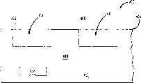
例如,图1A是带有其上覆盖有绝缘膜108的下导电层116半导体衬底118的剖面图,绝缘膜108带通孔115。按常规双嵌埋技术,在腐蚀了通孔115后进行将要形成的上层金属层的构图。参见图1B,在淀积构图金属层过程所用的光刻胶层102前,通常在绝缘层108上表面上淀积一层抗反射涂层113(现有技术已知为ARC)。ARC可以改善光刻分辨率。由于淀积了ARC,导致了在延伸到导电层116上大约“t”那么高的通孔115中有一层ARC残留物114。形成ARC层113后,通常在ARC层113上淀积光刻胶层102。然后根据掩模图形选择性曝光光刻胶层102。根据所用光刻胶是正性还是负性,在显影期间去掉曝光或未曝光部分,形成区110和112。然而,如图1B所示,ARC层114基本上不受光刻胶剥离操作的影响。For example, FIG. 1A is a cross-sectional view of a
为了形成多个沟槽,要去掉未由光刻胶保护的区110和112中的那部分ARC层113和绝缘层108。通过对晶片进行将有机ARC层113穿透的第一腐蚀工艺,及随后进行第二腐蚀,完成去除,以在绝缘膜108中形成所需沟槽。然而,通孔115中的ARC残留物114与腐蚀的产物反应,在通孔115内形成侧壁。通孔115中的这种侧壁具有ARC作用和氧化腐蚀并导致形成已有技术所称的屏障(图1C中的218)。屏障218一般基本与上述ARC残留物有相同的高度“t”。图1C是利用常规的双嵌埋技术上层金属光刻胶剥离后半导体衬底118的剖面图,衬底118上具有其上覆盖有绝缘层108的下金属116,该图展示了存在有屏障218。In order to form multiple trenches, the portions of
如现有技术已知的,合适的金属回流相当程度上取决于金属将淀积于其上的表面的表面几何形状。屏障218的存在妨碍了金属的回流,进而妨碍了金属顺利地流进通道槽212中。这种对金属流进通道槽212中的妨碍,会导致在通孔115中形成空洞。空洞的存在实际上增大了所形成的通道的电接触电阻。由于流过通道的所有电流必须由通道的没有空洞部分运载,所以空洞还会产生不可接受的可靠性问题。以此方式,通过通道的没有空洞部分的大电流密度会导致通道金属的电迁移。通道金属的电迁移会造成不可接受的长期时间失效(FIT)率。在某些情况下,由于屏障218妨碍了金属充分流到通孔115中或通道槽212中形成与下导电层116的电接触,所以会导致产生电开路,As is known in the art, suitable metal reflow depends considerably on the surface geometry of the surface on which the metal will be deposited. The presence of the
为了解决此问题,另一现有技术是在形成通孔之前在绝缘层表面上形成沟槽。然而,绝缘层表面没有平面化,不便于通孔的腐蚀。换言之,没有牺牲材料淀积到这些沟槽中以平面化绝缘层表面,不利于通孔的腐蚀。因此,把淀积以形成通孔掩模从而方便通道孔腐蚀的ARC和光刻胶材料淀积到这些槽中,并且一般与绝缘层上的不规则外形一致。不规则的绝缘层表面上的凹下和凸起造成了通孔腐蚀后,难以去除ARC和光刻胶材料。此外,还发现不规则的绝缘层表面上的凹下和凸起导致了光刻胶层难以分辨小表面几何形状。In order to solve this problem, another prior art is to form a trench on the surface of the insulating layer before forming the via hole. However, the surface of the insulating layer is not planarized, which is not convenient for the corrosion of the via hole. In other words, no sacrificial material is deposited into these trenches to planarize the surface of the insulating layer, detrimental to the etching of the vias. Accordingly, the ARC and photoresist materials deposited to form the via mask to facilitate via hole etch are deposited into these trenches and generally conform to the irregular topography on the insulating layer. Dimples and bumps on the surface of the irregular insulating layer make it difficult to remove the ARC and photoresist material after via etch. In addition, it was found that irregular dips and bumps on the surface of the insulating layer made it difficult for the photoresist layer to resolve small surface geometries.
所以需要消除常规双嵌埋技术产生的屏障及产生适于分辨小表面几何形状的基本平整表面的技术。There is therefore a need for techniques that eliminate the barriers created by conventional dual damascene techniques and produce substantially flat surfaces suitable for resolving small surface geometries.
概括地说,本发明涉及半导体器件,特别涉及穿过置于衬底上的叠层进行双嵌埋腐蚀的改进方法。根据本发明的一个实施例,该叠层包括下导电层和下导电层上的绝缘层。该方法包括以下操作步骤。首先,在绝缘层的上表面上形成沟槽,以便沟槽位于下导电层上,并借助于沟槽底部的绝缘材料与下导电层隔离。接着,在绝缘层的上表面上和沟槽内淀积可流动的氧化物,随后,平面化可流动氧化物至大概绝缘层上表面的水平。最后,穿通沟槽内的可流动氧化物和沟槽底部的绝缘材料向下腐蚀,直到下导电层,由此形成通道。In general, the present invention relates to semiconductor devices, and more particularly to an improved method for dual damascene etching through stacks disposed on a substrate. According to one embodiment of the present invention, the stack includes a lower conductive layer and an insulating layer on the lower conductive layer. The method includes the following steps. First, a trench is formed on the upper surface of the insulating layer so that the trench is located on the lower conductive layer and isolated from the lower conductive layer by means of an insulating material at the bottom of the trench. Next, a flowable oxide is deposited on the upper surface of the insulating layer and within the trenches, followed by planarization of the flowable oxide to approximately the level of the upper surface of the insulating layer. Finally, the flowable oxide in the trench and the insulating material at the bottom of the trench are etched down to the lower conductive layer, thereby forming a channel.
在另一实施例中,公开了一种形成用于连接下器件层和上层导电叠层的通孔的方法。在该公开的实施例中,上层导电层构形成位于形成在绝缘层中的沟槽中,并借助沟槽底部的绝缘材料与下器件层隔离。该方法包括以下步骤:在绝缘层上表面上及沟槽内淀积可流动氧化物;平面化可流动氧化物直到至少大概绝缘层上表面的水平;及穿通沟槽内的可流动氧化物及沟槽底部的绝缘材料向下腐蚀直到至少下器件层,由此形成通道。In another embodiment, a method of forming a via for connecting a lower device layer and an upper conductive stack is disclosed. In the disclosed embodiment, the upper conductive layer is configured to lie in a trench formed in the insulating layer and is isolated from the lower device layer by the insulating material at the bottom of the trench. The method comprises the steps of: depositing a flowable oxide on the upper surface of the insulating layer and in the trench; planarizing the flowable oxide to at least approximately the level of the upper surface of the insulating layer; and penetrating the flowable oxide in the trench and The insulating material at the bottom of the trench is etched down to at least the lower device layer, thereby forming the channel.
通过以下结合例示性展示本发明原理的附图对本发明的说明可以更清楚本发明的其它方案和优点。Other aspects and advantages of the present invention will become clearer through the following description of the present invention in conjunction with the accompanying drawings that exemplarily illustrate the principle of the present invention.
各附图例示性地展示了本发明,但并非限性的。为便于理解,下面的附图中类似的标号表示类同或类似的元件。The drawings illustrate the invention by way of illustration, but are not restrictive. For ease of understanding, similar reference numerals in the following drawings represent identical or similar elements.
图1A是利用常规双嵌埋技术形成通孔后带有其上覆盖有绝缘层的下导电层的半导体衬底的剖面图;FIG. 1A is a cross-sectional view of a semiconductor substrate with a lower conductive layer covered with an insulating layer after via holes are formed using a conventional double damascene technique;
图1B是显影金属光刻胶后图1A所示带有其上覆盖有绝缘层的下金属的半导体衬底的剖面图;1B is a cross-sectional view of the semiconductor substrate shown in FIG. 1A with the lower metal covered with an insulating layer after developing the metal photoresist;
图1C是金属光刻胶剥离后图1B所示带有其上覆盖有绝缘层的下金属的半导体衬底的剖面图;Figure 1C is a cross-sectional view of the semiconductor substrate with the lower metal covered with an insulating layer as shown in Figure 1B after the metal photoresist is stripped;
图2A是根据本发明一个实施例形成半导体结构400的一个阶段的剖面图;2A is a cross-sectional view of a stage in the formation of a
图2B是在深腐蚀了可流动氧化物以便基本上与绝缘层上表面共平面后,图2A所示本发明一个实施例的半导体结构的剖面图;Fig. 2B is a cross-sectional view of the semiconductor structure of one embodiment of the present invention shown in Fig. 2A after etching back the flowable oxide so as to be substantially coplanar with the upper surface of the insulating layer;
图2C是形成通孔后图2B所示本发明一个实施例的半导体结构的剖面图;FIG. 2C is a cross-sectional view of the semiconductor structure according to one embodiment of the present invention shown in FIG. 2B after forming via holes;
图2D是为金属淀积做准备时图2C所示本发明一个实施例的半导体结构的剖面图;Figure 2D is a cross-sectional view of the semiconductor structure of one embodiment of the present invention shown in Figure 2C in preparation for metal deposition;
图3是展示根据本发明一个实施例通过利用牺牲可流动氧化物的双嵌埋技术形成多级共平面金属/绝缘膜的流程图。FIG. 3 is a flowchart illustrating the formation of multi-level coplanar metal/insulator films by dual-buried technology using sacrificial flowable oxides according to one embodiment of the present invention.
下面将结合各附图中展示的几个例示性实施例详细说明本发明。在以下说明中,为便于充分理解本发明描述了许多特定细节。然而,所属领域的技术人员清楚,在不采用这些特定细节中的某一些或全部的情况下也可以实施本发明。另外一些情况下,为了对本发明不发生不必要地混淆,不再描述一些公知的工艺步骤。The present invention will be described in detail below with reference to several exemplary embodiments shown in the drawings. In the following description, numerous specific details are set forth in order to provide a thorough understanding of the present invention. It will be apparent, however, to one skilled in the art, that the present invention may be practiced without some or all of these specific details. In other instances, well known process steps have not been described in detail in order not to unnecessarily obscure the present invention.
本发明涉及形成多级共平面金属/绝缘膜的改进方法。根据本发明,通过利用牺牲可流动氧化物的双嵌埋技术实际上同时形成上金属层及到下器件层的电互连。The present invention relates to an improved method of forming multilevel coplanar metal/insulator films. According to the present invention, the upper metal layer and the electrical interconnects to the lower device layer are formed virtually simultaneously by dual damascene techniques utilizing sacrificial flowable oxides.
按本发明的一个实施例,通过利用可流动氧化物的双嵌埋腐蚀形成穿过绝缘层到达下器件层的通道。按所述的实施例,然后在位于下器件层上的绝缘层上表面上形成适于淀积金属的沟槽。然后可流动氧化物覆盖绝缘层的上表面,并将之平面化到大约为绝缘层上部的水平。有益的是,可流动氧化物的平面化形成了基本平整的表面,可以控制小表面几何形状的光刻分辨率及容易去除随后淀积的光刻材料。然后通过穿通沟槽内的可流动氧化物和沟槽底部的绝缘材料腐蚀到下器件层,由此形成通道。According to one embodiment of the invention, vias are formed through the insulating layer to the underlying device layer by a dual buried etch using a flowable oxide. According to the described embodiment, trenches suitable for depositing metal are then formed on the upper surface of the insulating layer overlying the underlying device layer. A flowable oxide then covers and planarizes the upper surface of the insulating layer to approximately the level of the upper portion of the insulating layer. Beneficially, planarization of the flowable oxide creates a substantially planar surface that allows control of lithographic resolution for small surface geometries and ease of removal of subsequently deposited lithographic materials. The channel is then formed by etching through the flowable oxide in the trench and the insulating material at the bottom of the trench to the underlying device layer.
下面结合图2A-3讨论本发明的各实施例。然而,所属领域的技术人员容易理解,这里相对于这些附图所述的细节只是例示性的,本发明可以延伸到这些限定性实施例的范围之外。Various embodiments of the present invention are discussed below in conjunction with FIGS. 2A-3. However, it will be readily understood by those skilled in the art that the details described herein with respect to these figures are by way of illustration only and the invention may extend beyond the scope of these limited embodiments.
图2A是本发明一个实施例的结构400的剖面图。如图所示,该结构包括衬底412,例如硅晶片。也可以利用例如砷化镓、锗、绝缘体上的硅(SOI)等其它半导体衬底或其它半导体材料。该衬底例如可以用预定导电类型的掺杂剂轻掺杂或重掺杂以得到所需电特性。该结构例如可以是用于制造包括nFET或pFET(场效应晶体管)的器件和包括电容和电阻的其它器件的结构。例如这些器件互连构成集成电路(IC)。这种IC包括随机存取存储器件(RAM)、动态随机存取存储器(SRAM)、同步DRAM(SDRAM)和只读存储器(ROM)。形成的其它IC包括专用集成电路(ASIC)或任何逻辑电路。一般情况下,在晶片上并行形成多个IC。处理完成后,将进行划片,将晶片分成分立芯片。然后封装芯片,形成例如最终用于如计算机系统、蜂窝电话、个人数字助手(PDAs)等用户产品及其它产品。然而,为了容易理解仅在形成IC方面说明本发明。另外,所说IC可以处于处理的任何阶段。Figure 2A is a cross-sectional view of a
例如,衬底包括形成于衬底内/上的部件(未示出)。这些部件对应于形成IC的器件。IC上包含有预先限定的器件层416,其中需要与另外导电层接触的层。一般情况下,器件层与其它器件层或部件借助介质材料隔离,可以将它们平面化得到平整表面413。器件层416例如是下金属层的一部分。或者,器件层是重掺杂的硅、多晶硅层或例如晶体管的源或漏区等任何类型的有源器件的一部分。在一个实施例中,器件层416是DRAM IC的位线。For example, the substrate includes features (not shown) formed in/on the substrate. These components correspond to devices forming an IC. Included on the IC are predefined device layers 416 where layers that need to be in contact with additional conductive layers. Generally, the device layer is isolated from other device layers or components by a dielectric material, which can be planarized to obtain a flat surface 413 . The
绝缘层418位于表面413上。绝缘层包括例如氧化硅等介质材料。可以是例如包括磷硅玻璃(PSG)、硼硅玻璃(BSG)或硼磷硅玻璃(BPSG)的掺杂硅酸盐玻璃等其它材料。还可以包括其它绝缘材料,例如聚酰亚胺等聚合物。绝缘层可以通过例如化学汽相淀(CVD)或其它淀积技术等淀积于衬底上。该实施例中,绝缘层418的厚度可以是约0.9-2.0微米。为提供平整的上表面,一般要平面化绝缘层。An insulating
使用常规光刻技术构图绝缘层,形成第一沟槽404。这种技术例如包括分别在晶片表面上淀积覆盖绝缘层的ARC和光刻胶层513和500。利用具有构图的掩模,用如深超紫外线(DUV)或极超紫外线(EUV)等来自曝光光源的辐射选择性曝光抗蚀剂层。也可以用产生不同于DUV和EUV波长辐射的其它曝光光源。根据所用的是正型还是负型抗蚀剂,显影去掉抗蚀剂层的曝光或未曝光的部分,露出对应于沟槽404的那部分绝缘层。在腐蚀室中各向异性腐蚀晶片以形成沟槽。各向异性腐蚀工艺例如包括反应离子腐蚀(RIE)。一般情况下,第一各向异性腐蚀工艺用于穿透有机ARC层。可以用如N2等腐蚀剂腐蚀ARC层。此后第二各向异性腐蚀去掉要求量的绝缘材料,形成沟槽。可以用如C4F8和O2等作为腐蚀源气腐蚀绝缘层。The insulating layer is patterned using conventional photolithography techniques to form the
如图所示,沟槽404是将与下器件层416接触的上金属层。上金属例如是导线。导线借助于随后形成的通孔(以下将讨论的)与器件层416电连接。导电层将与区416接触。这样一来,沟槽410的位置在区416之上。例如为导电线的沟槽410等其它沟槽位于限定的需要与之电接触的其它区之上。沟槽的深度和宽度取决于设计参数,例如薄层电阻和所用材料等。一般情况下,对腐蚀计时以得到所需深度。在某些实施例中,在绝缘层418上淀积第二绝缘层(未示出)。第二绝缘例如包括不同于第一绝缘材料的介质材料,并且可以对其进行选择腐蚀。这便可以将第一绝缘材料用作腐蚀停止层,由此限定沟槽的深度。这样一来,第一绝缘材料层不必很厚,同时第二绝缘层的厚度约等于由沟槽限定的导电线的厚度。形成沟槽404和410后,在绝缘层418的上表面406上淀积称作旋涂玻璃(SOG)的可流动氧化物层400。在所述的实施例中,可流动氧化物是构成SiO2的聚合化合物。可流动的氧化物例如是康宁制造的FOx。也可以使用其它可流动的氧化物和SOG。在一个实施例中,FOx用于填充沟槽。Fox通过旋涂工艺或任何其它常规淀积技术淀积。例如,可以通过常规SOG旋涂机用氢sile squioxane层涂敷衬底由此形成可流动氧化物。一种情况下,可以连续在150℃烘烤约一分钟,约250℃烘烤约一分钟和350℃烘烤约一分钟的同时以约1000-5000RPM旋涂涂敷材料。在某些情况下,因为可流动氧化物是牺牲层,所以可以省却固化步骤。层400的厚度应足以填充沟槽。可流动氧化物例如延伸到绝缘层418的上表面上406接近至少所要求的厚度“h”。一般情况下,h取决于工艺控制参数。例如,在某情况下层400可以约500nm厚。As shown, the
如图2B所示,然后深腐蚀可流动氧化层400,以便使之与绝缘层418的上表面406基本共平面。在所述实施例中,绝缘层418的上表面406用作腐蚀停止层。以此方式,形成基本平整的表面402,实际上与覆盖沟槽410的基本平整表面408同时覆盖了沟槽404。有益的是,绝缘层418的上表面406及表面402和408基本上表现为适于利用光刻法分辨小表面几何形状的表面。
参见图2C,形成适于互连下器件层和上金属层的穿过绝缘层的通孔的操作步骤如下。首先,在绝缘层418的上表面406和表面402及408上淀积ARC层513(一般是自然有机物)和光刻胶层500。接着,利用公知方法,在准备腐蚀先前存在的沟槽404中可流动氧化物和先前存在的沟槽404底部的绝缘层418中显影光刻胶层500,以形成通孔508。将晶片放置于氧化腐蚀室中,通过用N2腐蚀剂源气的已知为RIE的第一腐蚀工艺穿透显影的光刻胶所暴露区域中的有机ARC层513,由此腐蚀ARC层513。一旦腐蚀了ARC层513,利用C4F8腐蚀剂源气和第一数量的O2腐蚀源气腐蚀穿通先前存在的沟槽404中的可流动氧化物506,然后,用器件层416作腐蚀停止层,利用C4F8腐蚀剂源气和第二数量的O2腐蚀源气腐蚀穿通绝缘层418,由此形成通孔508。在所述实施例中,第一数量的腐蚀源气可以大于第二数量的腐蚀源气。Referring to FIG. 2C , the operation steps of forming a via hole through the insulating layer suitable for interconnecting the lower device layer and the upper metal layer are as follows. First, an ARC layer 513 (typically natural organic) and a
利用绝缘层518作腐蚀停止层,以相同方式去掉先前存在的沟槽410中的可流动氧化物。在一个实施例中,通过利用例如Ar、C4F8、CO和/或O2的RIE腐蚀衬底,从而去除可流动氧化物。The pre-existing flowable oxide in the
图2D是形成通孔508后本发明一个实施例的半导体结构400的剖面图。图2D中,沟槽410和404中的可流动氧化物已去掉,就如同ARC层和通孔腐蚀光刻胶掩模一样。2D is a cross-sectional view of
可以利用如化学汽相淀积(CVD)、物理汽相淀积(PVD)、或低压化学汽相淀积(LPCVD)等已知技术淀积金属层。选择用于CVD、PVD和LPCVD的特殊设备和工艺参数是半导体加工领域中的技术人员能力范围内的事。淀积金属(通常以覆盖整个半导体结构表面的方式)填充沟槽410和通道508,由此实际上同时形成上金属层和与下器件层416有关的通道互连。Metal layers may be deposited using known techniques such as chemical vapor deposition (CVD), physical vapor deposition (PVD), or low pressure chemical vapor deposition (LPCVD). Selection of particular equipment and process parameters for CVD, PVD and LPCVD is within the purview of those skilled in the semiconductor processing arts. Metal is deposited (typically in such a way as to cover the entire surface of the semiconductor structure) to fill
穿通所说可流动氧化物和所说绝缘材料的所说腐蚀包括根据第一腐蚀参数和第二腐蚀参数进行的,所说第一和第二参数中至少一个是利用包括C4F8的腐蚀源气。said etching through said flowable oxide and said insulating material comprises performing according to first etch parameters and second etch parameters, at least oneof said first and second parameters utilizing an etch comprisingC4F8 Origin Qi.
通过利用牺牲可流动氧化物的双嵌埋技术形成多级共平面的金属/绝缘膜的流程具体见图3,按本发明的一个实施例该流程可以包括以下操作步骤。The process of forming a multi-level coplanar metal/insulator film by using the dual-buried technology of sacrificial flowable oxide is specifically shown in FIG. 3 . According to an embodiment of the present invention, the process may include the following steps.
在步810,提供带有设置于衬底上的叠层的衬底。该叠层包括下器件层和在所说下器件层上的绝缘层。参见图2A,所示衬底为衬底412,所示下器件层为416。所示绝缘层418位于衬底和下器件层416上。At
在步815,在绝缘层上表面形成沟槽。该实施例中,沟槽位于下器件层上,绝缘层于沟槽底部和下器件层之间。参考图2A,所示沟槽为沟槽404。At
在步820,在绝缘层上表面上淀积可流动氧化物。该可流动氧化物在图2A中示出为可流动氧化物400。在所述实施例中,可流动氧化物是构成SiO2的聚合化合物。如上所述,可以通过旋涂工艺或所属领域的技术人员所知的任何常规方法进行淀积。At
在步825,平面化可流动氧化物层直到如图2B所示的绝缘层上表面的水平。然而,某些情况下,例如可以更进一步平面化到超出先前存在的绝缘层上表面的水平。In
图2C展示了如何在步830通过穿通沟槽404内的可流动氧化物和沟槽404底部的绝缘层418向下腐蚀到下器件层416从而形成通道508的情况。FIG. 2C shows how the
利用进行本发明双嵌埋腐蚀形成通道的所述方法可以实现许多优点。一个优点是,由于在绝缘层上表面上形成沟槽后再形成通孔,所以用所述流动氧化物的双嵌埋技术没有导致形成屏障。以此方式,由于淀积于绝缘层上表面上的ARC材料还没有形成,所以不会陷于通孔中。由于没有形成屏障,所以金属可以顺利地流进通孔中,方便了随后的金属淀积。以此方式,由于不存在屏障,所以流进通孔和沟槽中的金属基本上是均匀的,没有空洞。由于减少或基本消除了因存在金属空洞造成的局部电迁移,所以金属淀积的均匀性可以改善长期可靠性。A number of advantages can be realized using the described method of performing the dual buried etch of the present invention to form vias. An advantage is that the dual burying technique with the flowing oxide does not result in the formation of barriers since the vias are formed after the formation of the trenches on the upper surface of the insulating layer. In this way, since the ARC material deposited on the upper surface of the insulating layer has not yet formed, it will not become trapped in the via hole. Since no barrier is formed, metal can flow smoothly into the through hole, facilitating subsequent metal deposition. In this way, metal flow into the vias and trenches is substantially uniform without voids since there are no barriers. The uniformity of metal deposition improves long-term reliability by reducing or substantially eliminating localized electromigration due to the presence of metal voids.
本发明的另一优点是,可以在淀积ARC层前平面化可流动氧化物。由于适于分辨小面几何形状的光刻工艺的能力与其上淀积了ARC的表面的平整度有关,所以有益的是尽可能有平整的表面。如上所述,可流动氧化物可以形成平整的表面,便于在不改变最佳可用光学或电子束光刻设备的情况下的小几何分辨率,而常规双嵌埋技术则相反。Another advantage of the present invention is that the flowable oxide can be planarized prior to depositing the ARC layer. Since the ability of a photolithographic process suitable for resolving facet geometries is related to the flatness of the surface on which the ARC is deposited, it is beneficial to have as flat a surface as possible. As mentioned above, flowable oxides can form planar surfaces that facilitate small geometric resolutions without changing the best available optical or e-beam lithography equipment, as opposed to conventional dual-buried techniques.
通过所撰写的说明书可以清楚本发明的许多特点和优点,所以权利要求书将覆盖所有这些特点和优点。另外,由于所属领域的技术人员可以做出各种改形和改变,所以不希望本发明限于所述和所示的精确结构和操作步骤。因此,所有合适的改形和等同物皆隐含于本发明的范围内。The many features and advantages of the invention are apparent from the written description, and it is therefore intended that the claims cover all such features and advantages. Furthermore, since various modifications and changes may occur to those skilled in the art, it is not intended that the present invention be limited to the precise construction and operation described and shown. Accordingly, all suitable modifications and equivalents are implied to fall within the scope of the present invention.
Claims (25)
Translated fromChineseApplications Claiming Priority (3)
| Application Number | Priority Date | Filing Date | Title |
|---|---|---|---|
| US08/884,861US6300235B1 (en) | 1997-06-30 | 1997-06-30 | Method of forming multi-level coplanar metal/insulator films using dual damascene with sacrificial flowable oxide |
| US884,861 | 1997-06-30 | ||
| US884861 | 1997-06-30 |
Publications (2)
| Publication Number | Publication Date |
|---|---|
| CN1208949Atrue CN1208949A (en) | 1999-02-24 |
| CN1146956C CN1146956C (en) | 2004-04-21 |
Family
ID=25385585
Family Applications (1)
| Application Number | Title | Priority Date | Filing Date |
|---|---|---|---|
| CNB981156274AExpired - Fee RelatedCN1146956C (en) | 1997-06-30 | 1998-06-30 | Method of forming multi-level coplanar metal/insulator films using dual damascene with sacrificial flowable oxide |
Country Status (7)
| Country | Link |
|---|---|
| US (1) | US6300235B1 (en) |
| EP (1) | EP0895283B1 (en) |
| JP (1) | JPH1187352A (en) |
| KR (1) | KR100494955B1 (en) |
| CN (1) | CN1146956C (en) |
| DE (1) | DE69837313T2 (en) |
| TW (1) | TW462112B (en) |
Cited By (2)
| Publication number | Priority date | Publication date | Assignee | Title |
|---|---|---|---|---|
| CN100463075C (en)* | 2004-02-25 | 2009-02-18 | 国际商业机器公司 | Method of making data tracks for use in magnetic shift register memory devices |
| CN102592989A (en)* | 2011-01-07 | 2012-07-18 | 中国科学院微电子研究所 | Near-interface planarization back-etching method for interlayer dielectric |
Families Citing this family (28)
| Publication number | Priority date | Publication date | Assignee | Title |
|---|---|---|---|---|
| US7205635B1 (en) | 1998-03-20 | 2007-04-17 | Mcsp, Llc | Hermetic wafer scale integrated circuit structure |
| US7215025B1 (en)* | 1998-03-20 | 2007-05-08 | Mcsp, Llc | Wafer scale semiconductor structure |
| US6982475B1 (en) | 1998-03-20 | 2006-01-03 | Mcsp, Llc | Hermetic wafer scale integrated circuit structure |
| US6965165B2 (en) | 1998-12-21 | 2005-11-15 | Mou-Shiung Lin | Top layers of metal for high performance IC's |
| JP3214475B2 (en)* | 1998-12-21 | 2001-10-02 | 日本電気株式会社 | Method of forming dual damascene wiring |
| US6727143B1 (en)* | 1999-11-30 | 2004-04-27 | Advanced Micro Devices, Inc. | Method and system for reducing charge gain and charge loss when using an ARC layer in interlayer dielectric formation |
| JP2001332621A (en)* | 2000-03-13 | 2001-11-30 | Toshiba Corp | Semiconductor device and manufacturing method thereof |
| US6521542B1 (en)* | 2000-06-14 | 2003-02-18 | International Business Machines Corp. | Method for forming dual damascene structure |
| US6576550B1 (en)* | 2000-06-30 | 2003-06-10 | Infineon, Ag | ‘Via first’ dual damascene process for copper metallization |
| JP3704030B2 (en)* | 2000-07-24 | 2005-10-05 | シャープ株式会社 | Manufacturing method of semiconductor device |
| US6465358B1 (en)* | 2000-10-06 | 2002-10-15 | Intel Corporation | Post etch clean sequence for making a semiconductor device |
| US6514860B1 (en)* | 2001-01-31 | 2003-02-04 | Advanced Micro Devices, Inc. | Integration of organic fill for dual damascene process |
| US6372635B1 (en) | 2001-02-06 | 2002-04-16 | Advanced Micro Devices, Inc. | Method for making a slot via filled dual damascene low k interconnect structure without middle stop layer |
| TW478133B (en)* | 2001-02-27 | 2002-03-01 | Nanya Technology Corp | Manufacturing method of the bit line contact plug of semiconductor memory cell |
| KR100405934B1 (en)* | 2001-12-26 | 2003-11-14 | 주식회사 하이닉스반도체 | Method for manufacturing a contact hole of semiconductor device |
| KR100428791B1 (en)* | 2002-04-17 | 2004-04-28 | 삼성전자주식회사 | Method of forming dual damascene interconnection using low dielectric material |
| TW546771B (en)* | 2002-05-13 | 2003-08-11 | Nanya Technology Corp | Manufacturing method of dual damascene structure |
| KR100454130B1 (en)* | 2002-05-28 | 2004-10-26 | 삼성전자주식회사 | Method of forming dual damascene interconnection using low dielectric material |
| TW544857B (en)* | 2002-07-30 | 2003-08-01 | Promos Technologies Inc | Manufacturing method of dual damascene structure |
| KR100442147B1 (en)* | 2002-08-09 | 2004-07-27 | 동부전자 주식회사 | Method for forming dual damascene pattern |
| US7538025B2 (en)* | 2003-11-14 | 2009-05-26 | Taiwan Semiconductor Manufacturing Company | Dual damascene process flow for porous low-k materials |
| KR100624098B1 (en) | 2005-06-16 | 2006-09-15 | 삼성전자주식회사 | Thin film structure and formation method thereof |
| KR100703560B1 (en)* | 2005-12-28 | 2007-04-03 | 동부일렉트로닉스 주식회사 | Metal wiring formation method of semiconductor device |
| US8062971B2 (en) | 2008-03-19 | 2011-11-22 | Infineon Technologies Ag | Dual damascene process |
| US7696056B2 (en)* | 2008-05-02 | 2010-04-13 | Micron Technology, Inc. | Methods of forming capacitors |
| US7618874B1 (en)* | 2008-05-02 | 2009-11-17 | Micron Technology, Inc. | Methods of forming capacitors |
| US8629037B2 (en)* | 2011-09-24 | 2014-01-14 | Taiwan Semiconductor Manufacturing Company, Ltd. | Forming a protective film on a back side of a silicon wafer in a III-V family fabrication process |
| CN108538839B (en)* | 2017-03-01 | 2019-08-23 | 联华电子股份有限公司 | Semiconductor structure, semiconductor structure for memory element and manufacturing method thereof |
Family Cites Families (7)
| Publication number | Priority date | Publication date | Assignee | Title |
|---|---|---|---|---|
| KR940010197A (en) | 1992-10-13 | 1994-05-24 | 김광호 | Manufacturing Method of Semiconductor Device |
| US5449644A (en)* | 1994-01-13 | 1995-09-12 | United Microelectronics Corporation | Process for contact hole formation using a sacrificial SOG layer |
| JP3778299B2 (en) | 1995-02-07 | 2006-05-24 | 東京エレクトロン株式会社 | Plasma etching method |
| TW388083B (en)* | 1995-02-20 | 2000-04-21 | Hitachi Ltd | Resist pattern-forming method using anti-reflective layer, resist pattern formed, and method of etching using resist pattern and product formed |
| US5614765A (en)* | 1995-06-07 | 1997-03-25 | Advanced Micro Devices, Inc. | Self aligned via dual damascene |
| US5935877A (en) | 1995-09-01 | 1999-08-10 | Applied Materials, Inc. | Etch process for forming contacts over titanium silicide |
| ES2268894T3 (en)* | 1998-12-18 | 2007-03-16 | Scios Inc. | AGONISTS AND ANTAGONISTS OF BENZODIAZEPIN RECEPTORS OF PERIPHERAL TYPE. |
- 1997
- 1997-06-30USUS08/884,861patent/US6300235B1/ennot_activeExpired - Lifetime
- 1998
- 1998-06-05DEDE69837313Tpatent/DE69837313T2/ennot_activeExpired - Lifetime
- 1998-06-05EPEP98110307Apatent/EP0895283B1/ennot_activeExpired - Lifetime
- 1998-06-17TWTW087109645Apatent/TW462112B/ennot_activeIP Right Cessation
- 1998-06-22KRKR10-1998-0023337Apatent/KR100494955B1/ennot_activeExpired - Fee Related
- 1998-06-30CNCNB981156274Apatent/CN1146956C/ennot_activeExpired - Fee Related
- 1998-06-30JPJP10184376Apatent/JPH1187352A/enactivePending
Cited By (3)
| Publication number | Priority date | Publication date | Assignee | Title |
|---|---|---|---|---|
| CN100463075C (en)* | 2004-02-25 | 2009-02-18 | 国际商业机器公司 | Method of making data tracks for use in magnetic shift register memory devices |
| CN102592989A (en)* | 2011-01-07 | 2012-07-18 | 中国科学院微电子研究所 | Near-interface planarization back-etching method for interlayer dielectric |
| CN102592989B (en)* | 2011-01-07 | 2015-04-08 | 中国科学院微电子研究所 | Near-interface planarization back-etching method for interlayer dielectric |
Also Published As
| Publication number | Publication date |
|---|---|
| JPH1187352A (en) | 1999-03-30 |
| US6300235B1 (en) | 2001-10-09 |
| KR19990007191A (en) | 1999-01-25 |
| DE69837313D1 (en) | 2007-04-26 |
| CN1146956C (en) | 2004-04-21 |
| EP0895283B1 (en) | 2007-03-14 |
| DE69837313T2 (en) | 2007-12-20 |
| EP0895283A3 (en) | 2000-05-03 |
| TW462112B (en) | 2001-11-01 |
| EP0895283A2 (en) | 1999-02-03 |
| KR100494955B1 (en) | 2005-09-09 |
Similar Documents
| Publication | Publication Date | Title |
|---|---|---|
| CN1208949A (en) | Method of forming multi-level coplanar metal/insulator films using dual damascene with sacrificial flowable oxide | |
| EP0667036B1 (en) | Chip interconnection having a breathable etch stop layer | |
| CN1152413C (en) | Improved dual damascene structure | |
| US7470616B1 (en) | Damascene wiring fabrication methods incorporating dielectric cap etch process with hard mask retention | |
| KR100571417B1 (en) | Dual damascene wiring of semiconductor device and manufacturing method thereof | |
| TW202238843A (en) | Method for manufacturing semiconductor structure | |
| CN119650518B (en) | Method for preparing semiconductor structure and semiconductor structure | |
| US9136164B2 (en) | Semiconductor device and fabrication method | |
| US7253112B2 (en) | Dual damascene process | |
| US20010016413A1 (en) | Semiconductor device and method of manufacturing a semiconductor device with reduced contact failures | |
| US20030186529A1 (en) | Method of manufacturing semiconductor device having opening | |
| US6664162B2 (en) | Method of manufacturing capacitor | |
| CN111211095B (en) | Method for manufacturing conductive interconnection line | |
| US20160276213A1 (en) | Reliable contacts | |
| KR20000072897A (en) | method of manufacturing semiconductor device | |
| KR101147387B1 (en) | Manufacturing method of semiconductor device | |
| US20250308986A1 (en) | Back end of line (beol) interconnection approach | |
| KR100414733B1 (en) | A method for forming a metal-insulator-metal capacitor | |
| HK1016342A (en) | Method of forming multi-level coplanar metal/insulator films using dual damascene with sacreficial flowable oxide | |
| KR20030038521A (en) | Process for fabricating a semiconductor device | |
| KR100506050B1 (en) | Contact formation method of semiconductor device | |
| US20070010089A1 (en) | Method of forming bit line of semiconductor device | |
| KR100415988B1 (en) | Method for forming a via hole | |
| KR20070079807A (en) | Manufacturing Method of Semiconductor Device | |
| KR20030056923A (en) | method for manufacturing a metal line |
Legal Events
| Date | Code | Title | Description |
|---|---|---|---|
| C06 | Publication | ||
| PB01 | Publication | ||
| C10 | Entry into substantive examination | ||
| SE01 | Entry into force of request for substantive examination | ||
| C14 | Grant of patent or utility model | ||
| GR01 | Patent grant | ||
| ASS | Succession or assignment of patent right | Owner name:INFINEON TECHNOLOGIES AG Free format text:FORMER OWNER: SIEMENS AKTIENGESELLSCHAFT Effective date:20130225 | |
| C41 | Transfer of patent application or patent right or utility model | ||
| TR01 | Transfer of patent right | Effective date of registration:20130225 Address after:German Neubiberg Patentee after:Infineon Technologies AG Address before:Munich, Germany Patentee before:Siemens AG Effective date of registration:20130225 Address after:Munich, Germany Patentee after:QIMONDA AG Address before:German Neubiberg Patentee before:Infineon Technologies AG | |
| C41 | Transfer of patent application or patent right or utility model | ||
| TR01 | Transfer of patent right | Effective date of registration:20151223 Address after:German Berg, Laura Ibiza Patentee after:Infineon Technologies AG Address before:Munich, Germany Patentee before:QIMONDA AG | |
| CF01 | Termination of patent right due to non-payment of annual fee | Granted publication date:20040421 Termination date:20160630 | |
| CF01 | Termination of patent right due to non-payment of annual fee |