CN1207747C - Plasma body display screen arc shaped electrode structure - Google Patents
Plasma body display screen arc shaped electrode structureDownload PDFInfo
- Publication number
- CN1207747C CN1207747CCN 02148495CN02148495ACN1207747CCN 1207747 CCN1207747 CCN 1207747CCN 02148495CN02148495CN 02148495CN 02148495 ACN02148495 ACN 02148495ACN 1207747 CCN1207747 CCN 1207747C
- Authority
- CN
- China
- Prior art keywords
- electrode
- arc
- electrodes
- electrode structure
- shaped
- Prior art date
- Legal status (The legal status is an assumption and is not a legal conclusion. Google has not performed a legal analysis and makes no representation as to the accuracy of the status listed.)
- Expired - Fee Related
Links
Images
Landscapes
- Gas-Filled Discharge Tubes (AREA)
- Devices For Indicating Variable Information By Combining Individual Elements (AREA)
Abstract
Description
Translated fromChinese技术领域technical field
本发明涉及彩色等离子体显示屏的电极结构,属于平板显示技术领域。The invention relates to an electrode structure of a color plasma display screen, belonging to the technical field of flat panel display.
背景技术Background technique
彩色等离子体显示器(Plasma Display Panel,简称PDP),是利用气体放电产生真空紫外光(VUV)激发三基色荧光粉而产生红绿蓝三基色光,然后经过空间和时间的调制实现彩色图像显示。The color plasma display (Plasma Display Panel, referred to as PDP) uses gas discharge to generate vacuum ultraviolet light (VUV) to excite three primary color phosphors to generate red, green and blue three primary color light, and then realizes color image display through space and time modulation.
对于表面放电型彩色PDP显示屏,主要有如下电极结构:For the surface discharge color PDP display, there are mainly the following electrode structures:
1.条形透明电极和汇流(BUS)电极结构;1. Strip transparent electrode and bus (BUS) electrode structure;
2.T型透明电极和汇流(BUS)电极结构;2. T-shaped transparent electrode and bus (BUS) electrode structure;
3.格栅形电极结构;3. Grid electrode structure;
4.多电极电极结构。4. Multi-electrode electrode structure.
上述四种结构均采用直线型电极结构,电极间的放电面积小,使发光亮度和发光效率低。且上述电极结构中,条形透明电极和汇流(BUS)电极与T型透明电极和汇流(BUS)电极结构采用了透明电极和BUS电极的复合结构,工艺成本高,对位精度要求高,电极间的电容大。The above four structures all adopt the linear electrode structure, and the discharge area between the electrodes is small, so that the luminous brightness and luminous efficiency are low. Moreover, in the above electrode structure, the strip-shaped transparent electrode and the bus (BUS) electrode and the T-shaped transparent electrode and the bus (BUS) electrode structure adopt a composite structure of the transparent electrode and the BUS electrode, the process cost is high, and the alignment accuracy is high. The capacitance between them is large.
发明内容Contents of the invention
本发明的目的是提出一种表面放电型彩色PDP显示屏维持电极和扫描电极,将维持电极和扫描电极设计成由弧形电极组成的结构,以降低PDP工艺成本,提高发光效率和发光亮度。The purpose of the present invention is to propose a surface discharge type color PDP display sustain electrode and scan electrode, the sustain electrode and scan electrode are designed to be formed by the structure of arc electrode, to reduce PDP process cost, improve luminous efficiency and luminous brightness.
本发明的目的可以通过以下设计来达到:The purpose of the present invention can be achieved by the following designs:
一种等离子体显示屏弧形电极结构,包括维持电极和扫描电极,其特征是在维持电极中,独立单元由圆弧形电极和弧形电极两端的短路电极和内部的短路电极组成,各独立单元由公共电极连接而成维持电极;在扫描电极中,独立单元由圆弧形电极和弧形电极两端的短路电极和内部的短路电极组成,各独立单元由公共电极连接而成扫描电极;或维持电极和扫描电极由呈波浪状连接的多弧形电极组成。A arc-shaped electrode structure of a plasma display screen, including sustain electrodes and scan electrodes, is characterized in that in the sustain electrodes, independent units are composed of arc-shaped electrodes, short-circuit electrodes at both ends of the arc-shaped electrodes and internal short-circuit electrodes, each independently The cells are connected by a common electrode to form a sustain electrode; in the scan electrode, the independent cells are composed of arc-shaped electrodes, short-circuit electrodes at both ends of the arc-shaped electrodes and internal short-circuit electrodes, and each independent cell is connected by a common electrode to form a scan electrode; or The sustain electrodes and the scan electrodes are composed of multi-arc electrodes connected in a wave shape.
本发明的目的还可以通过以下设计来达到:The purpose of the present invention can also be achieved by the following designs:
维持电极和扫描电极由弧形透明电极和汇流电极组成。Sustain electrodes and scan electrodes are composed of curved transparent electrodes and bus electrodes.
上述圆弧形电极为多条同心圆弧或同弧圆弧。The above-mentioned arc-shaped electrodes are a plurality of concentric arcs or arcs of the same arc.
本发明相比现有技术具有如下优点:Compared with the prior art, the present invention has the following advantages:
1.由于采用弧形电极结构,维持电极和扫描电极间的有效面积增加,使显示屏的发光亮度和发光效率提高。1. Due to the arc-shaped electrode structure, the effective area between the sustain electrode and the scan electrode is increased, so that the luminous brightness and luminous efficiency of the display screen are improved.
2.采用多弧形电极结构,放电电极间的间隙由小到大增加,可以保证在不提高显示屏工作电压的基础上实现大间距气体放电,使显示屏的发光亮度和发光效率提高。2. The multi-arc electrode structure is adopted, and the gap between the discharge electrodes increases from small to large, which can ensure large-space gas discharge without increasing the operating voltage of the display screen, and improve the luminous brightness and luminous efficiency of the display screen.
3.采用多弧形电极结构,电极一次性制作,可以保证电极间间隙的一致性,有利于提高显示屏的性能。3. The multi-arc electrode structure is adopted, and the electrodes are made at one time, which can ensure the consistency of the gap between electrodes and help improve the performance of the display screen.
4.采用多弧形电极结构不要求制作透明电极,不仅省去了电极间的一次精密对位,而且可以节省工艺成本。4. The use of multi-arc electrode structure does not require the production of transparent electrodes, which not only saves a precise alignment between electrodes, but also saves process costs.
5.由于无透明电极,电极间的电容下降,使彩色PDP显示屏功耗减小。5. Since there is no transparent electrode, the capacitance between the electrodes decreases, which reduces the power consumption of the color PDP display.
附图说明Description of drawings
图1是同弧-多弧形电极结构的示意图;Fig. 1 is the schematic diagram of same arc-multi-arc electrode structure;
图2是同心-多弧形电极结构的示意图;Fig. 2 is the schematic diagram of concentric-multi-arc electrode structure;
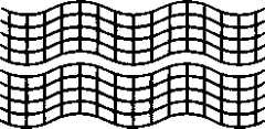
图3是波浪-多弧形电极结构的示意图。Fig. 3 is a schematic diagram of a wave-multi-arc electrode structure.
具体实施方式Detailed ways
下面结合附图对本发明作进一步描述,但不是对本发明的限制。The present invention will be further described below in conjunction with the accompanying drawings, but the present invention is not limited thereto.
图1是维持电极和扫描电极上的多弧电极均为相同圆弧电极的情况,如图所示,在维持电极中,独立单元由多条相同圆弧形电极2和弧形电极两端的短路电极3和内部的短路电极4组成,各独立单元由公共电极1连接而形成维持电极;同样的,在扫描电极中,独立单元由相同圆弧形电极6和弧形电极两端的短路电极7和内部的短路电极8组成,各独立单元由公共电极5连接而形成扫描电极。上述结构中,维持电极和扫描电极可以互换,对彩色PDP显示屏的工作不会导致影响。Figure 1 is the case where the multi-arc electrodes on the sustain electrodes and the scan electrodes are all the same arc electrodes. As shown in the figure, in the sustain electrodes, the independent unit is composed of multiple same arc electrodes 2 and short circuits at both ends of the arc electrodes. The electrodes 3 and the internal short-circuit electrodes 4 are composed, and each independent unit is connected by the common electrode 1 to form a sustain electrode; similarly, in the scanning electrode, the independent units are composed of the same arc-shaped electrode 6 and the short-circuit electrodes 7 and The internal short-circuit electrodes 8 are formed, and each independent unit is connected by a common electrode 5 to form a scanning electrode. In the above structure, the sustain electrode and the scan electrode can be interchanged, which will not affect the operation of the color PDP display.
在图1所示的多弧形电极结构中,弧与弧之间等间距排列,且间距为d,则维持电极中的弧形电极与扫描电极中的弧形电极间的距离可以是d、2d、3d、4d、5d---,当电极间施加电压脉冲后,放电将优先在某一最适合放电的电极间开始,然后向其它的弧形电极间扩展,使放电区域不仅因为采用弧形电极而扩大,而且间距大的电极间的放电具有更高的发光亮度和发光效率。In the multi-arc electrode structure shown in Figure 1, the arcs are arranged at equal intervals and the interval is d, then the distance between the arc electrodes in the sustain electrodes and the arc electrodes in the scan electrodes can be d, 2d, 3d, 4d, 5d ---, when the voltage pulse is applied between the electrodes, the discharge will preferentially start between a certain electrode that is most suitable for discharge, and then expand to other arc-shaped electrodes, so that the discharge area is not only due to the use of arc Shaped electrodes are expanded, and the discharge between electrodes with large spacing has higher luminous brightness and luminous efficiency.
图2所示为采用同心圆弧形电极的情况,弧与弧之间的距离沿圆弧直径方向以整数倍变化,也同样可以达到扩大放电区域面积和提高发光亮度和发光效率的作用。Figure 2 shows the case of using concentric arc-shaped electrodes. The distance between the arcs changes in integer multiples along the diameter of the arcs, which can also achieve the effect of expanding the area of the discharge area and improving the luminous brightness and luminous efficiency.
由图1、图2可知,采用多弧形电极结构,可以省去透明电极制作以降低成本,并且可以提高发光亮度和发光效率。It can be seen from Figure 1 and Figure 2 that the use of multi-arc electrode structure can save the production of transparent electrodes to reduce costs, and can improve luminous brightness and luminous efficiency.
图1、图2所示的独立单元电极结构存在必须与选址电极进行精密对位的问题,为此可以采用如图3所示电极结构。The electrode structures of independent units shown in Figure 1 and Figure 2 have the problem that they must be precisely aligned with the addressing electrodes, so the electrode structure shown in Figure 3 can be used.
在图3所示的电极结构中,维持和扫描电极均由呈波浪状连接的多弧形电极组成,选址放电在维持电极和扫描电极的任一位置进行时,放电状况均相同,所以选址电极与维持和扫描电极间不需要精密对位。采用图3所示电极结构,单元内部的放电过程与图1、图2所示电极结构相同。In the electrode structure shown in Figure 3, both the sustain and scan electrodes are composed of multi-arc electrodes connected in a wave shape. No precise alignment is required between the address electrodes and the sustain and scan electrodes. Using the electrode structure shown in Figure 3, the discharge process inside the cell is the same as the electrode structure shown in Figure 1 and Figure 2.
本发明的具体实施方案以图2所示结构和在表面放电式彩色交流PDP中应用为例加以说明,如果采用反射式结构,则将维持电极和扫描电极制作在彩色PDP显示屏的前基板上,根据设计要求可在电极之上制作透明介质和MgO层。后基板上的选址电极方向与前基板上的维持和扫描电极方向垂直,选址电极上根据设计要求可以分别制作介质层、障壁和荧光粉层,选址电极和维持电极进行精密对位后进行封接、排气,充气、封离后制作成彩色PDP显示屏。为了使彩色PDP显示屏的单元开口率高,本发明要求电极宽度应尽可能的精细,电极可以采用金属薄膜电极用光刻法制作,或采用光敏银浆材料用光刻法制作,对单元节距大的彩色PDP显示屏,也可以采用精密丝网印刷法制作。The specific embodiment of the present invention is illustrated by taking the structure shown in Figure 2 and its application in the surface discharge color AC PDP as an example. If a reflective structure is adopted, the sustain electrodes and scan electrodes are made on the front substrate of the color PDP display , according to the design requirements, a transparent medium and MgO layer can be made on the electrode. The direction of the addressing electrodes on the rear substrate is perpendicular to the direction of the sustaining and scanning electrodes on the front substrate. The dielectric layer, barrier rib and phosphor layer can be made on the addressing electrodes according to the design requirements. After precise alignment of the addressing electrodes and the sustaining electrodes After sealing, exhausting, inflating and sealing off, it is made into a color PDP display. In order to make the cell aperture ratio of the color PDP display screen high, the present invention requires that the electrode width should be as fine as possible, and the electrodes can be made by photolithography using metal thin film electrodes, or by photolithography using photosensitive silver paste materials. The color PDP display screen with large pitch can also be made by precision screen printing.
本发明的显示屏驱动方式可以采用现有的PDP显示屏的驱动方式,也可以根据本发明显示屏的一些特点,设计最佳驱动波形。The driving mode of the display screen of the present invention can adopt the driving mode of the existing PDP display screen, and can also design the optimal driving waveform according to some characteristics of the display screen of the present invention.
Claims (3)
Priority Applications (1)
| Application Number | Priority Date | Filing Date | Title |
|---|---|---|---|
| CN 02148495CN1207747C (en) | 2002-12-11 | 2002-12-11 | Plasma body display screen arc shaped electrode structure |
Applications Claiming Priority (1)
| Application Number | Priority Date | Filing Date | Title |
|---|---|---|---|
| CN 02148495CN1207747C (en) | 2002-12-11 | 2002-12-11 | Plasma body display screen arc shaped electrode structure |
Publications (2)
| Publication Number | Publication Date |
|---|---|
| CN1414595A CN1414595A (en) | 2003-04-30 |
| CN1207747Ctrue CN1207747C (en) | 2005-06-22 |
Family
ID=4751451
Family Applications (1)
| Application Number | Title | Priority Date | Filing Date |
|---|---|---|---|
| CN 02148495Expired - Fee RelatedCN1207747C (en) | 2002-12-11 | 2002-12-11 | Plasma body display screen arc shaped electrode structure |
Country Status (1)
| Country | Link |
|---|---|
| CN (1) | CN1207747C (en) |
Families Citing this family (3)
| Publication number | Priority date | Publication date | Assignee | Title |
|---|---|---|---|---|
| KR100536215B1 (en)* | 2003-08-05 | 2005-12-12 | 삼성에스디아이 주식회사 | Plasma display panel |
| KR100673437B1 (en)* | 2004-12-31 | 2007-01-24 | 엘지전자 주식회사 | Plasma display panel |
| CN102376511B (en)* | 2010-09-30 | 2014-03-19 | 四川虹欧显示器件有限公司 | PDP (Plasma Display Panel) discharge electrode and PDP display comprising same |
- 2002
- 2002-12-11CNCN 02148495patent/CN1207747C/ennot_activeExpired - Fee Related
Also Published As
| Publication number | Publication date |
|---|---|
| CN1414595A (en) | 2003-04-30 |
Similar Documents
| Publication | Publication Date | Title |
|---|---|---|
| CN1632901A (en) | display device for display | |
| JP2001307646A (en) | Gas discharge panel | |
| CN1207747C (en) | Plasma body display screen arc shaped electrode structure | |
| CN1179393C (en) | flat panel display | |
| CN1557009A (en) | plasma display | |
| CN1713328A (en) | plasma display panel | |
| CN1822291A (en) | Plasma display panel and its forming method | |
| CN1841632A (en) | plasma display panel | |
| CN1707578B (en) | display device | |
| CN1763897A (en) | plasma display panel | |
| CN1832090A (en) | plasma display panel | |
| CN1658363A (en) | Plasma display panel and manufacturing method thereof | |
| KR100326882B1 (en) | Plasma Display Panel and Discharging Method of The Same | |
| CN1855350A (en) | Plasma display panel | |
| CN1223978C (en) | Plasma display with low starting voltage | |
| KR100366946B1 (en) | Plasma Display Panel | |
| KR100351465B1 (en) | Plasma Display Panel and Method Of Driving The Same | |
| CN1302505C (en) | Addressing Electrode Structure of Plasma Flat Panel Display | |
| KR100353953B1 (en) | Plasma Display Panel | |
| CN1310274C (en) | Transparent Electrode Structure of Plasma Flat Panel Display | |
| CN1731555A (en) | plasma display panel | |
| CN1203511C (en) | Coplanar electrode surface site selection surface discharge plasma body display screen | |
| JP2001118520A (en) | Gas discharge panel | |
| CN100350544C (en) | AC Plasma Display | |
| CN100511560C (en) | Tank-type electrode for plasma display board |
Legal Events
| Date | Code | Title | Description |
|---|---|---|---|
| C06 | Publication | ||
| PB01 | Publication | ||
| C10 | Entry into substantive examination | ||
| SE01 | Entry into force of request for substantive examination | ||
| C14 | Grant of patent or utility model | ||
| GR01 | Patent grant | ||
| CF01 | Termination of patent right due to non-payment of annual fee | ||
| CF01 | Termination of patent right due to non-payment of annual fee | Granted publication date:20050622 Termination date:20171211 |