CN1196615A - Wideband Low Noise Low Intermodulation Distortion Receiver - Google Patents
Wideband Low Noise Low Intermodulation Distortion ReceiverDownload PDFInfo
- Publication number
- CN1196615A CN1196615ACN 97103771CN97103771ACN1196615ACN 1196615 ACN1196615 ACN 1196615ACN 97103771CN97103771CN 97103771CN 97103771 ACN97103771 ACN 97103771ACN 1196615 ACN1196615 ACN 1196615A
- Authority
- CN
- China
- Prior art keywords
- signal
- low
- frequency
- output
- drain electrode
- Prior art date
- Legal status (The legal status is an assumption and is not a legal conclusion. Google has not performed a legal analysis and makes no representation as to the accuracy of the status listed.)
- Granted
Links
- 238000013461designMethods0.000claimsabstractdescription14
- 230000005855radiationEffects0.000claimsabstract2
- 239000000872bufferSubstances0.000claimsdescription49
- 239000003990capacitorSubstances0.000claimsdescription19
- 230000010355oscillationEffects0.000claimsdescription19
- 230000003321amplificationEffects0.000claimsdescription15
- 238000003199nucleic acid amplification methodMethods0.000claimsdescription15
- 230000003139buffering effectEffects0.000claimsdescription9
- 230000000694effectsEffects0.000claimsdescription8
- 239000013078crystalSubstances0.000claimsdescription6
- 230000002411adverseEffects0.000claimsdescription5
- 238000001914filtrationMethods0.000claimsdescription4
- 230000009467reductionEffects0.000claimsdescription4
- 230000010363phase shiftEffects0.000claimsdescription3
- 230000009466transformationEffects0.000claims1
- 230000008878couplingEffects0.000abstractdescription4
- 238000010168coupling processMethods0.000abstractdescription4
- 238000005859coupling reactionMethods0.000abstractdescription4
- 230000010354integrationEffects0.000abstract1
- 238000010586diagramMethods0.000description12
- 238000006243chemical reactionMethods0.000description9
- 238000000034methodMethods0.000description7
- 230000002265preventionEffects0.000description5
- 230000009471actionEffects0.000description4
- 230000008569processEffects0.000description4
- 238000012545processingMethods0.000description4
- 230000001965increasing effectEffects0.000description3
- 230000002093peripheral effectEffects0.000description3
- 230000002457bidirectional effectEffects0.000description2
- 230000000903blocking effectEffects0.000description2
- 230000008859changeEffects0.000description2
- 238000005259measurementMethods0.000description2
- 230000007246mechanismEffects0.000description2
- 238000009966trimmingMethods0.000description2
- GYHNNYVSQQEPJS-UHFFFAOYSA-NGalliumChemical compound[Ga]GYHNNYVSQQEPJS-UHFFFAOYSA-N0.000description1
- 229910001218Gallium arsenideInorganic materials0.000description1
- 238000004891communicationMethods0.000description1
- 230000008094contradictory effectEffects0.000description1
- 238000001514detection methodMethods0.000description1
- KWLSQQRRSAWBOQ-UHFFFAOYSA-NdipotassioarsanylpotassiumChemical compound[K][As]([K])[K]KWLSQQRRSAWBOQ-UHFFFAOYSA-N0.000description1
- 230000009977dual effectEffects0.000description1
- 230000005672electromagnetic fieldEffects0.000description1
- 238000005516engineering processMethods0.000description1
- 238000002474experimental methodMethods0.000description1
- 230000005669field effectEffects0.000description1
- 238000007667floatingMethods0.000description1
- 229910052733galliumInorganic materials0.000description1
- 230000001939inductive effectEffects0.000description1
- 238000007689inspectionMethods0.000description1
- 238000004519manufacturing processMethods0.000description1
- 238000007781pre-processingMethods0.000description1
- 239000004065semiconductorSubstances0.000description1
- 238000001228spectrumMethods0.000description1
- 230000001629suppressionEffects0.000description1
- 238000010897surface acoustic wave methodMethods0.000description1
Images


Landscapes
- Superheterodyne Receivers (AREA)
- Amplifiers (AREA)
Abstract
Description
Translated fromChinese本发明关于一种宽频带接收机,特别是一种适用于很宽的射频信号频率范围的单晶集成电路接收机。The present invention relates to a wide-band receiver, in particular to a single-crystal integrated circuit receiver suitable for a wide frequency range of radio frequency signals.
随着高频通信系统的广泛使用,高质量的宽频带接收机的需求与日俱增,而传统的接收机如电视调谐器已逐渐无法完全满足需求。另外,结合个人电脑调谐器,已往使用离散元件的设计,亦因体积太大而无法使用,取而代之的是射频单晶集成电路宽频带接收机。With the widespread use of high-frequency communication systems, the demand for high-quality broadband receivers is increasing day by day, and traditional receivers such as TV tuners have gradually been unable to fully meet the needs. In addition, combined with a personal computer tuner, the design using discrete components in the past was too large to be used, and it was replaced by a radio frequency single crystal integrated circuit wideband receiver.
其于上述理由,许多使用集成电路设计的接收机应运而生。图1A为一典型的电视/VCR接收机的设计,整个接收机电路包括:UHF输入滤波器20、VHF输入滤波器21、两个低噪音射频放大器22与2.3、两个中间级滤波24与25、砷化钾调谐器集成电路26,振荡谐振回路27、中频滤波器28、中频放大器外围回路29与除法器30等。此接收机先利用两不同的滤波回路20、21与差动式低噪音放大器22、23,配合Bu与Bv两个波段控制信号,将射频信号分为VHF/CATV与UHF两种信号后分别加以放大,然后导入不同的中间级滤波回路24、25以完成个别的追踪滤波动作,处理后的两个信号又分别导入调谐器集成电路26内。图1B为调谐器集成电路26的内部方块图,其中包括:波段切换开关261、UHF波段用振荡器262、VHF/CATV波段用振荡器263、振荡输出缓冲器264、双向平衡式调制器265、及中频放大器266等回路。导入此集成电路26的两个信号先进入波段切换开关261,用Bv控制信号来选择是由VHF/CATV波段信号或是由UHF波段信号通过进入调制器265。另外,使用Bu控制信号切换使用集成电路外相对应波段的谐振回路。频道锁定动作则由振荡器输出信号给除法器30(图1)配合锁相回路控制器(未显示于图上)来完成。将经适当切换输出的射频信号与本地振荡信号导入调制器混合调制,其输出经集成电路26外的中频滤波器28检出后再导入集成电路内的中频放大器29放大,其最终的中频输出放大倍率则由另一个U/V增益控制信号Bm来控制。此接收机虽已使用射频集成电路来设计,但由于该集成电路的电气特性并不理想,特别如噪音系数大于8dB,需要在集成电路外增加许多离散元件回路来改善,因此对UHF高频波段特性造成不浪影响。For the above reasons, many receivers designed using integrated circuits have emerged. Fig. 1A is the design of a typical TV/VCR receiver, and the whole receiver circuit includes:
图2A为一个卫星电视调谐接收机,其适宜和射频信号频率范围从950MHz到2GHz。整个系统除了一个射频集成电路40外,外围电路仅有一组谐振回路41与几个耦合电容CA与CB,组成非常简单。此集成电路40由射频放大器RFAMP、混波调制器MIX、本地振荡器OSC与中频放大器IFAMP所组成。此集成电路40的中频输入端IF应有一个中频滤波器连接于该处(图2A中未显示)。Figure 2A is a satellite TV tuner receiver suitable for radio frequencies ranging from 950 MHz to 2 GHz. In addition to a radio frequency integrated
此集成电路使用特殊的提升型砷化镓金属半导体场效应晶体管制程,有别于一般常用的空乏型制程;此外,图2A所示电路的最大特色乃是使用如图2B所示的多向振动式振荡器,配合适当的外接谐振回路,可以在相当宽的频率范围中得到负电阻特性,显示其为良好的宽频带振荡器,另外由于其输出为差动式,故可以直接导入双向平衡调制器。This integrated circuit uses a special boosted GaAs metal-semiconductor field-effect transistor process, which is different from the commonly used depletion-type process; in addition, the biggest feature of the circuit shown in Figure 2A is the use of multi-directional vibration as shown in Figure 2B With the appropriate external resonant circuit, the negative resistance characteristic can be obtained in a wide frequency range, which shows that it is a good broadband oscillator. In addition, because its output is differential, it can be directly imported into two-way balanced modulation. device.
此接收机虽然构造简单,但其噪音系数大于10dB而且仅适宜用于卫星电视频道,无法应用于一般的有线或无线电视,实用性受到极大限制。Although the structure of this receiver is simple, its noise figure is greater than 10dB and is only suitable for satellite TV channels, and cannot be applied to general cable or wireless TV, and its practicability is greatly limited.
图3显示一种适用于有线电视(CATV)的集成化调谐器系统。此系统采用两次频率转换结构,先使用一个坤化镓升频转换器集成电路50将输入的50-550MHz的射频信号经过集成电路内的低噪音自动增益控制放大器501的放大处理后,与集成电路内的第一本地振荡器503的输出一起导入集成电路内的混波器502做混波调制处理,再将其输出导入集成电路外的第一中频滤波器51,检出升频转换后的第一中频信号(如700MHz),此信号再与集成电路外的第二本地振荡53输出一起导入集成电路外的第二混波器52做调制,其输出导入第二中频滤波器检出降频转换后的45MHz中频信号。经过上述电路处理之后,整个系统大致还能满足CATV调谐器的电气规格。但是,此设计仅适用于CATV的频率范围50-550MHz。此外,由于使用晶体管的线性工作区做自动增益控制,能调制的信号强度范围甚小,对于大的射频信号的放大失真与中频输出的强度固定有不利的影响。另外,由于使用两次频率转换机构,而集成电路内仅集成了第一次频率转换电路,必须耗费较多的外接元件来完成第二次频率转换功能,无法精简系统构装。Figure 3 shows an integrated tuner system for CATV. This system adopts two frequency conversion structures. First, a gallium kunide up-converter
综上所述,习知的接收机仍有许多总是待改善:首先,接收机适用频宽有待增加,否则无法扩展其应用;接收机本身的电气特性如低噪音系数、良好的放大器线性度、低互调失真与振荡器的低相位噪音均须特别加以改善,以期能满足更高画质数码电视接收机的高品质要求;再则,为了能设计携带型的微型接收机,不得不使用单晶射频集成电路来取代大部分的离散元件设计,而集成电路外接电路数目必须降到最低;最后,使用单纯而成熟的集成电路制程以降低生产成本也是不可忽略的任务。To sum up, the known receivers still have a lot to be improved: First, the applicable bandwidth of the receiver needs to be increased, otherwise its application cannot be expanded; the electrical characteristics of the receiver itself, such as low noise figure and good amplifier linearity , low intermodulation distortion and low phase noise of the oscillator must be specially improved in order to meet the high-quality requirements of higher-quality digital television receivers; moreover, in order to design portable micro-receivers, we have to use Single crystal radio frequency integrated circuits replace most of the discrete component designs, and the number of external circuits connected to integrated circuits must be reduced to a minimum; finally, using a simple and mature integrated circuit process to reduce production costs is also a task that cannot be ignored.
基于以上要求,本发明提出一种可集成化的全差动式低噪音低互调失真宽频带接收机,其特性综合如下:Based on the above requirements, the present invention proposes an integratable fully differential low-noise low-intermodulation distortion wide-band receiver whose characteristics are summarized as follows:
(1)适宜用于很宽的射频信号频率范围,可以涵盖有线电视的50到550MHz、VHF/UHF无线电视的50到900MHz与卫星电视的950MHz到2GHz甚至更高的频率应用(视微波集成电路制程的技术,可适用于例如5GHz)。(1) It is suitable for a wide frequency range of radio frequency signals, which can cover 50 to 550MHz for cable TV, 50 to 900MHz for VHF/UHF wireless TV, and 950MHz to 2GHz for satellite TV or even higher frequency applications (see microwave integrated circuits) process technology, applicable to eg 5GHz).
(2)在上述的频率范围实现下列功能:(2) Realize the following functions in the above frequency range:
(a)小于6dB的低噪音系数:(a) Low noise figure less than 6dB:
(b)低互调失真,指定频道信号强度为60dBμV时,非指定频道信号强度必须大于95dBμV以上,才能在中频信号上造成1%的互调失真率;(b) Low intermodulation distortion. When the signal strength of the designated channel is 60dBμV, the signal strength of the non-designated channel must be greater than 95dBμV to cause 1% intermodulation distortion rate on the intermediate frequency signal;
(c)输入阻抗值几乎为固定(典型值为75Ω或50Ω);(c) The input impedance value is almost fixed (typically 75Ω or 50Ω);
(3)整个系统采用差动式回路设计,所有高频信号均用双耦合走线,不易受零电位地面浮动干扰,系统稳定。另外,由于双耦合线正负两端信号紧密结合,能量较少辐射外漏,易于通过电磁场安全检验;(3) The whole system adopts a differential loop design, and all high-frequency signals use double-coupled wiring, which is not easily disturbed by zero-potential ground floating, and the system is stable. In addition, because the signals at the positive and negative ends of the double-coupled line are closely combined, the energy is less radiated and leaked, and it is easy to pass the electromagnetic field safety inspection;
(4)系统内核心部分各电路间均采用主动元件直流耦合,可以很容易的集成为晶元面积非常小的集成电路,再加上其周边配合电路少,可以轻易的设计成高品质微型接收机系统。(4) All the circuits in the core part of the system are DC-coupled with active components, which can be easily integrated into an integrated circuit with a very small wafer area. In addition, there are few peripheral matching circuits, and it can be easily designed into a high-quality micro-receiver machine system.
本发明的宽频带低噪音低互调失真接收机,包含:差动式低噪音放大器,接收输入的差动式或单端射频信号而将其放大,具有低噪音系数与大信号低放大失真特性,并完成输入阻抗匹配与输出差动信号的功能;第一缓冲器,接收该差动式低噪音放大器的输出信号,具有直流偏压调整、输出缓冲与逆流防止等功能;第一电压/电流转换器,接收该第一缓冲器的输出信号,将会造成严重的信号放大失真的大振幅电压信号线性地转换成相对振幅较小的电流信号;自动增益控制放大器,接收该第一电压/电流转换器所输出的电流信号,并利用中频输出振幅传感器接进来的增益控制信号调整放大器的放大或缩小倍率,使得其输出信号的振幅维持固定大小;第二缓冲器,接收该自动增益控制放大器的输出信号,同于该第一缓冲器亦具有直流偏压调整、输出缓冲与逆流防止等功能;追踪滤波器,接收该第二缓冲器的输出信号,并根据输入的控制信号而仅使指定频率的射频信号通过,而将其他信号滤掉;第二电压/电流转换器,接收该追踪滤波器所输出的具有指定频率的射频信号,将大振幅电压信号线性地转换成相对振幅较小的电流信号;压控振荡器核心、谐振器、第二缓冲器及锁相回路控制器,四者共同构成一完整的锁相回路系统,其连接关系为该谐振器接收该锁相回路控制器的控制信号以决定振荡频率,该压控振荡器核心连接于该谐振器,而振出具有该振荡频率的信号,然后该振出的信号再经过该第三缓冲器而进入该锁相回路控制器,该第二缓冲器同样地具有直流偏压调整、输出缓冲与逆流防止等功能,该锁相回路控制器接收频道数据指令而输出波段控制信号与频率微调信号供该谐振器与该追踪滤波器所用;调制器,接收来自该第二电压/电流转换器与该第三缓冲器的两组信号,而输出信号为该两组信号的乘积;第四缓冲器,接收该调制器的输出信号,同样具有直流偏压调整、输出缓冲与逆流防止等功能;中频滤波器,接收该第四缓冲器的输出信号,用以检出最终的中频信号供尔后信号解调之用。The wide-band low-noise and low-intermodulation-distortion receiver of the present invention includes: a differential low-noise amplifier, which receives and amplifies an input differential or single-ended radio frequency signal, and has characteristics of low noise figure and large signal low amplification distortion , and complete the functions of input impedance matching and output differential signal; the first buffer receives the output signal of the differential low noise amplifier, and has the functions of DC bias adjustment, output buffering and reverse current prevention; the first voltage/current The converter receives the output signal of the first buffer, and linearly converts the large-amplitude voltage signal that will cause serious signal amplification and distortion into a current signal with a relatively small amplitude; the automatic gain control amplifier receives the first voltage/current The current signal output by the converter, and the gain control signal connected to the intermediate frequency output amplitude sensor is used to adjust the amplification or reduction ratio of the amplifier, so that the amplitude of the output signal remains fixed; the second buffer receives the automatic gain control amplifier. The output signal, like the first buffer, also has the functions of DC bias adjustment, output buffering and backflow prevention; the tracking filter receives the output signal of the second buffer, and only makes the specified frequency according to the input control signal The RF signal passes through while other signals are filtered out; the second voltage/current converter receives the RF signal with a specified frequency output by the tracking filter, and linearly converts the large-amplitude voltage signal into a relatively small-amplitude current Signal; the core of the voltage-controlled oscillator, the resonator, the second buffer and the phase-locked loop controller, the four together form a complete phase-locked loop system, and the connection relationship is that the resonator receives the control of the phase-locked loop controller The signal is used to determine the oscillation frequency, the core of the voltage controlled oscillator is connected to the resonator, and a signal with the oscillation frequency is oscillated, and then the oscillating signal enters the phase-locked loop controller through the third buffer, the first The two buffers also have the functions of DC bias adjustment, output buffering, and backflow prevention. The phase-locked loop controller receives channel data instructions and outputs band control signals and frequency fine-tuning signals for the resonator and the tracking filter; modulation The device receives two sets of signals from the second voltage/current converter and the third buffer, and the output signal is the product of the two sets of signals; the fourth buffer receives the output signal of the modulator, which also has DC The functions of bias voltage adjustment, output buffering and backflow prevention; the intermediate frequency filter receives the output signal of the fourth buffer to detect the final intermediate frequency signal for subsequent signal demodulation.
此外,本发明的宽频带低噪音低互调失真接收机还包含:前置选择滤波器,输入的差动式或单端射频信号进入差动式低噪音放大器之前,先进入此前置选择滤波器,用以初步选择指定频道附近的信号,并视需要而完成阻抗转换的功能。In addition, the wide-band low-noise and low-intermodulation distortion receiver of the present invention also includes: a pre-select filter, and before the input differential or single-ended radio frequency signal enters the differential low-noise amplifier, it first enters the pre-select filter The device is used to initially select the signal near the specified channel, and complete the function of impedance conversion as needed.
图1A为一习知技术的电视/VCR接收机的设计;Fig. 1A is the design of a television/VCR receiver of the prior art;
图1B为图1A所示接收机中调谐器集成电路26的内部方块图;FIG. 1B is an internal block diagram of the tuner integrated circuit 26 in the receiver shown in FIG. 1A;
图2A为一习知技术的卫星电视调谐接收机的设计;Fig. 2A is the design of a satellite TV tuning receiver of the prior art;
图2B为与图2A的接收机所使用的多向振动式振荡器;FIG. 2B is a multi-directional vibration oscillator used in the receiver of FIG. 2A;
图3为一习知技术的适用于有线电视的集成调谐器系统;Fig. 3 is an integrated tuner system suitable for cable television of a prior art;
图4A为本发明的宽频带低噪音低互调失真接收机的方块图;Fig. 4A is the block diagram of wideband low noise low intermodulation distortion receiver of the present invention;
图4B为本发明的宽频带低噪音低互调失真接收机的另一实施例的方块图;FIG. 4B is a block diagram of another embodiment of the broadband low-noise low-intermodulation distortion receiver of the present invention;
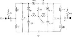
图5A为图4B中的前置选择滤波器15在差动输入下的实际电路;Fig. 5 A is the actual circuit of the
图5B为图4B中的前置选择滤波器15在单端输入下的实际电路;Fig. 5B is the actual circuit of
图5C为图5A或图5B的电路应用于多频道波段系统时的接法;Fig. 5C is the connection method when the circuit of Fig. 5A or Fig. 5B is applied to a multi-channel band system;
图6表示图4中的低噪音放大器1的较佳实施例;Figure 6 shows a preferred embodiment of the
图7表示图6所示电路在相当宽的频域范围内所测量的输入阻抗;Figure 7 shows the measured input impedance of the circuit shown in Figure 6 over a relatively wide frequency domain;
图8为图4中的缓冲器2的较佳实施例;Figure 8 is a preferred embodiment of the
图9为图4中的电压/电流转换器3与自动增益控制放大器4的较佳实施例;FIG. 9 is a preferred embodiment of the voltage/
图10为射频信号经图4中的1至6部分的处理后,所得到的噪音系数值;Fig. 10 is the noise figure value obtained after the radio frequency signal is processed by
图11A为图4中的压控振荡器核心8的较佳实施例;FIG. 11A is a preferred embodiment of the
图11B为图4中的谐振器9的较佳实施例;Fig. 11 B is a preferred embodiment of the
图12表示利用图11A与图11B所共同构成的压控振荡器电路进行自由振荡的结构,其中图12A与图12B分别表示80MHz以下与4GHz以上的自由振荡输出;Fig. 12 shows the structure of free oscillation using the voltage-controlled oscillator circuit composed of Fig. 11A and Fig. 11B, wherein Fig. 12A and Fig. 12B represent the free-oscillation output below 80 MHz and above 4 GHz respectively;
图13A与图13B表示对图11A与图11B所共同构成的压控荡器电路进行频率切换所得结果;FIG. 13A and FIG. 13B show the frequency switching results of the voltage-controlled oscillator circuit composed of FIG. 11A and FIG. 11B;
图14为图4中调制器11、转换器7部分的较佳实施例;Fig. 14 is the preferred embodiment of
图15为互调失真测量的示意图;Fig. 15 is a schematic diagram of intermodulation distortion measurement;
图16用以表示本发明的接收机具有非常低的互调失真;Fig. 16 is used to show that the receiver of the present invention has very low intermodulation distortion;
图17为本发明的接收机用于有线电视与一般无线电视的情况下所需的实际硬件图;Fig. 17 is the actual hardware diagram needed under the situation that the receiver of the present invention is used for cable TV and general wireless TV;
图18为本发明的接收机用于卫星电视的情况下所需的实际硬件图。Fig. 18 is a diagram of actual hardware required in the case where the receiver of the present invention is used for satellite television.
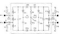
图4A表示本发明的系统方块图,其中包括:差动式低噪音低失真宽频带放大器1(简称差动式低噪音放大器或LNA);直流耦合缓冲器2(简称缓冲器或BUF);电压/电流线性转换器3(简称转换器或V/I);差动式低失真自动增益控制放大器4(简称自动增益控制放大器或AGC);直流耦合缓冲器5(简称缓冲器或BUF);差动式追踪滤波器6(简称IF);电压/电流线性转换器7(简称转换器或V/I);差动式压控振荡器核心8(简称压控振荡器或VCOC);可调整差动式谐振器9(简称谐振器或DCR);直流耦合缓冲器10(简称缓冲器或BUF);低失真双向平衡式调制器11(简称调制器或MIX);直流耦合缓冲器12(简称缓冲器或BUF);中频滤波器13(简称IFF);及锁相回路控制器14(简称PLLC),其中虚线所包围的部分表示作在同一颗集成电路上。Fig. 4 A shows the system block diagram of the present invention, which includes: differential low noise low distortion broadband amplifier 1 (abbreviated differential low noise amplifier or LNA); DC coupled buffer 2 (abbreviated buffer or BUF); voltage /current linear converter 3 (referred to as converter or V/I); differential low-distortion automatic gain control amplifier 4 (referred to as automatic gain control amplifier or AGC); DC-coupled buffer 5 (referred to as buffer or BUF); Dynamic tracking filter 6 (referred to as IF); voltage/current linear converter 7 (referred to as converter or V/I); differential voltage controlled oscillator core 8 (referred to as voltage controlled oscillator or VCOC); adjustable differential Dynamic resonator 9 (abbreviated as resonator or DCR); DC-coupled buffer 10 (referred to as buffer or BUF); low-distortion bidirectional balanced modulator 11 (referred to as modulator or MIX); DC-coupled buffer 12 (abbreviated as buffer device or BUF); an intermediate frequency filter 13 (referred to as IFF); and a phase-locked loop controller 14 (referred to as PLLC), wherein the part surrounded by a dotted line indicates that they are on the same integrated circuit.
图4B表示本发明的另一实施例的系统方块图,其不同于图4A之处仅在于多了一个前置选择滤波器。FIG. 4B shows a system block diagram of another embodiment of the present invention, which is different from FIG. 4A only in that there is an additional preselection filter.
此接收机的适用射频频率范围极宽,从40MHz到3GHz或更高,其输入信号为天线所截下的信号或有线同轴电缆所送至的信号,可以是单端或差动信号输入。The applicable RF frequency range of this receiver is extremely wide, from 40MHz to 3GHz or higher, and its input signal is the signal cut off by the antenna or the signal sent by the wired coaxial cable, which can be single-ended or differential signal input.
图4B的接收机系统中,输入的射频信号以差动或单端(RFin-端接地)方式先进入差动前置选择滤波器15,此前置选择滤波器15为一带通滤波器,其频带及中心频率由来自锁相回路控制器144频率微调信号VTu与频道波段切换信号BSs控制,以使选定的频道信号通过,而尽可能将不用的频道信号滤掉,以降低其他频道干扰正常信号的可能,此前置选择滤波器15的输出信号进入低噪音放大器1。In the receiver system of Fig. 4B, the input radio frequency signal first enters the
另一方面,图4A的接收机系统中,输入的射频信号以差动或单端方式直接进入低噪音放大器1。On the other hand, in the receiver system of FIG. 4A , the input RF signal directly enters the
低噪音放大器1用以作信号放大,其除了具有低噪音系数外,并具有大信号低放大失真特性,且完成输入阻抗匹配及输出差动信号二项功能。低噪音放大器1的差动信号输出经过缓冲器2的直流偏压调整、输出缓冲与逆流防止等处理之后,依平衡的方式用双耦合线接至转换器3,然后再经过自动增益控制放大器4作自动增益控制放大,其中转换器3的作用在于将会造成严重信号放大失真的大振幅电压信号线性地转换成相对振幅较小的电流信号,然后经自动增益控制放大器4再将此电流信号以最小的失真程度转换成适当的电压输出信号。另外,自动增益控制放大器4利用由中频输出振幅传感器接进来的增益控制信号GCs调整放大器的放大或缩小倍率,使得不管射频输入的信号振幅如何变化,自动增益控制放大器4的输出信号振幅均能维持固定大小。The low-
自动增益控制放大器4的输出信号经过缓冲器5处理后进入追踪滤波器6,它根据从锁相回路控制器14输出的频率微调信号VTu作为追踪控制信号与频道波段切换信号BSs改变其频率选择特性,令其只追踪欲通过的指定频率的射频信号而将不要的信号滤掉,其输出RFout+与RFout-做为调制器11的一组输入(先经过转换器7)。The output signal of the automatic gain control amplifier 4 is processed by the
调制器11的另一组输入从压控振荡器核心8输出经缓冲器10进入,该组信号亦输出至锁相回路控制器14作频道锁定之用,而压控振荡器核心8所需的谐振回路则由谐振器9提供。由外部介面回路所提供的频道数据DCs输入锁相回路控制器14,使其产生相对应的频率微调信号VTu,用来调整谐振器9内可变电容的适当谐振电容值,同时藉由回路压控振荡器核心8、谐振器9、缓冲器10及锁相回路控制器14之间的锁相回路动作以锁定精确的振荡信号输出。Another set of input of the
此外,为了扩大压控振荡器的振荡频率范围,谐振器9被设计成可调整差动式谐振回路,它接收从锁相回路控制器14进入的频道波段切换信号BSs来改变不同的谐振电感值,藉以切换不同的频道波段。除此之外,锁相回路控制器14还利用信号VTu做为追踪滤波控制信号,使其进入追踪滤波器6改变该回路内的可变电容的电容值与切换对应波段的电感值,以完成追踪滤波的功能。此外,追踪滤波器6的频率选择特性也能降低系统的噪音系数与互调失真率。In addition, in order to expand the oscillation frequency range of the voltage-controlled oscillator, the
转换器7与调制器11构成一低互调失真调制器,其中转换器7接收来自追踪滤波器6的输出信号(电压信号),将此振幅甚大的电压信号转换成相对振幅较小的电流信号,调制器11将此组电流信号与来自压控荡器核心8、经过缓冲器10的信号做双向平衡式信号混合调制。由于转换器7的事先处理再加上差动式低噪音放大器1、缓冲器2、转换器3、自动增益控制放大器4及缓冲器5等回路的低放大失真特性,调制器11的互调失真可以降到最低程度。调制之后的信号再经过缓冲器12的缓冲处理后,输出至中频滤波器13,检出所需的差动中频信号IFout+与IFout-。The
由于从外界输入的射频信号涵盖所有频道,为了尽可能减少非指定频道信号对指定频道信号的干扰,可采取如图4 B所示的方块图构造,其中在低噪音放大器1之前使用一个前置选择滤波器15,其仅容许指定频道附近的频带的信号通过。图5A与图5B分别为差动式输入与单端输入的情况下前置选择滤波器15的实际电路的较佳实施例,以下说明图5A所示电路的动作:图5A为一切换差动式前置选择滤波器,其输入信号为全频道的射频差动信号,切换二极管D1、D2受波段切换信号Bx为高值时才能进入双谐振式带通滤波器(图5A中虚线包围的部分),其中包含两组谐振回路:L1、L2、L3为第一组谐振回路的电感,对应于不同的频道波段有不同的等效电感,这些电感还提供阻抗转换的功能,其中L2电感自中间抽头接一大电阻R5到地,以提供切换二极管D1、D2的直流偏压路径;C、C2与可变电容VD1为第一组谐振回路的电容,透过频率微调信号VTu可改变VD1的电容值,因而改变等效电容值。同理,第二组谐振回路的电感为L1a、L2a与L3a,而电容为C1a、C2a与VD1a。此外,C3与VD2为两组谐振回路间的耦合电容,可通过微调VD2的电容值而改变其耦合量。经由以上说明,可知通过波段切换信号Bx与频率微调信号VTu的共同作用,可改变滤波器的中心频率,而可调式滤波选择功能。同理,切换二极管D3与D4受波段切换信号Bx的控制,仅当Bx为高值时滤波所得的信号才能进入下一级的低噪音放大器1。图5B为单端输入情况下的实际电路,其操作原理类似于图5A,在此不加赘述。Since the radio frequency signal input from the outside covers all channels, in order to minimize the interference of the non-designated channel signal to the designated channel signal, a block diagram structure as shown in Figure 4 B can be adopted, in which a front end is used before the low noise amplifier 1 A
图5C为图5A或图5B的电路应用于多频道波段系统时的接法,其中每一方块均表示一个如图5A或图5B的滤波器。每一滤波器接受的频率微调信号VTu相同,但波段切换信号Bx则彼此独立,由于各滤波器具有不同的等效电感,因此形成中心频率各不相同的带通滤波器。可视需要将多个滤波器如图5C的方式接在一起,而在需要的频带处(单一或多个)产生带通滤波效果。FIG. 5C is a connection method when the circuit in FIG. 5A or FIG. 5B is applied to a multi-channel band system, wherein each block represents a filter as in FIG. 5A or FIG. 5B . Each filter receives the same frequency trimming signal VTu, but the band switching signal Bx is independent of each other. Since each filter has a different equivalent inductance, it forms a bandpass filter with different center frequencies. Multiple filters can be connected together as shown in FIG. 5C as required, so as to produce bandpass filtering effect at the desired frequency band (single or multiple).
此外,基于前置选择滤波器15之噪音系数对于整个系统之噪音系数影响甚大,在设计上要放宽前置选择滤波器15的频率选择性,以保证其损耗在1dB以下。In addition, since the noise figure of the
经过前置选择滤波器15处理后的信号在进入混波器之前,必须先经过低噪音放大器1、缓冲器2、转换器3、自动增益控制放大器4、缓冲器5及追踪滤波器6的前置处理,其主要功能包括低噪音低失真放大、自动增益控制及信号选择追踪等。首先,由于前置选择滤波器15损耗的极小处理,整个系统的噪音系数几乎由低噪音放大器1决定,为了追求最低噪音系数,此电路一般无采用数量最少的低噪音主动元件,并且避免在射频信号路径上直接串接电阻元件作输入阻抗匹配,而改用电感或电容反馈回路来同时完成噪音与输入阻抗匹配的最佳化设计。然而,此放大器若未作特殊线性化处理,往往造成较大的非线性失真。另一方面,在此频率范围下,最佳化的电感或电容反馈值往往因为太大而无法集成于IC之内。另外,由于自动增益控制放大器4通常接收较大的输入信号,为了防止严重的放大失真,必须做特殊的线性化处理。Before entering the mixer, the signal processed by the
为了同时实现低噪音与低失真两个相互矛盾的特性,本发明采用低噪音放大器与自动增益控制放大器电路分离的思路,请参考图4中的1、2、3、4及5的部分,其中如前所述,将低噪音放大器1设计成具有非常低的噪音系数,而将自动增益控制放大器4设计成具有低失真特性。In order to realize the two contradictory characteristics of low noise and low distortion at the same time, the present invention adopts the idea of separating the low noise amplifier and the automatic gain control amplifier circuit, please refer to the
图6为图4中之低噪音放大器1的较佳实施例,主动元件Q1与Q2构成一组差动配对,此差动配对结合输出电组对R1与R2、需要的电流源Is1及适当的偏压Bias组合成差动放大器,此外,在电流电压有余裕度(head room)下,可以在Q1与Q2上层叠另一组差动配对Q3与Q4来增加差动器的放大倍率。射频信号以差动方式(晶体管Q1、Q2的栅极电压分别为RFin+、Rfin-)或单端(晶体管Q1、Q2的栅极电压分别为RFin+、GND)输入Q1与Q2的栅极,经过放大之后,由Q3与Q4的漏极(若未接Q3与Q4,则由Q1与Q2的漏极)以差动方式输出。除此之外,为了增加电路的稳定性与线性度,使用两组负反馈被动回路Zf1与Zf2由输出端接至输入端,而此被动回路可为电阻与电容的串接回路或其它类似回路,同时它们亦提供此差动放大器所须的宽频域固定输入阻抗特性(典型值为75Ω)。图7表示图6所示电路在相当宽的频域范围内(约50MHz-3GHz)所测得的输入阻抗,其大小均在75Ω-87Ω之间。FIG. 6 is a preferred embodiment of the
低噪音放大器1的输出进入自动增益控制放大器4之前先经过如图8所示的直流耦合缓冲器(相当于图4中的缓冲器2),其中Q5与Q6配合适当的电流源Is2与Is3分别作为正向与负向输出的源极追随器,它们具有防止信号逆流的功能,而由其源极输出的等倍信号经过适当数目的二极管做直流降压后,提供下一级电路的输入信号与适当的输入级晶体管偏压。Before the output of the
图9为一般常用的全向差动式自动增益控制放大器电路,其增益大小可由上方两个差动控制信号电压差ΔV来决定,持续减少此差值以得到-40dB以上的增益抑制倍率。请注意下半部由晶体管Q7与Q8、电阻RfIs3与Is4所组成的电路用以将电压转成电流(相当于图4中的转换器3),如前所述,此电路大大地改善放大器的线性度。Figure 9 is a commonly used omnidirectional differential automatic gain control amplifier circuit. Its gain can be determined by the voltage difference ΔV of the two upper differential control signals. Continuously reduce this difference to obtain a gain suppression ratio above -40dB. Please note that the lower part is composed of transistors Q7 and Q8, resistors RfIs3 and Is4 to convert voltage into current (equivalent to
参考图4,自动增益控制放大器4的输出亦经过直流缓冲器5处理后再接出到下一级的追踪滤波器6。追踪滤波器6的功能与前置选择滤波器15相同,其实际电路亦如图5所示。但由于其损耗对系统的噪音系数影响甚小,故设计上着重于其频率选择性,换而言之,虽然追踪滤波器6与前置选择滤波器15均可用图5所示的电路来完成,但两者具有不同的电路元件主值,将追踪滤波器6设计成具有较窄的通过频带。追踪滤波器6的作用除了减小频道互扰外,并改善噪音系数。Referring to FIG. 4 , the output of the automatic gain control amplifier 4 is also processed by the
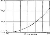
图10为射频信号经上述电路处理之后,在相当宽的频域范围内(约50MHz-3GHz)所得到的噪音系数值(使用pseudo-morphic High Electfon Mobility Transistor,PHEMT元件),清楚地显示出此电路结构的噪音系数甚低(小于4.8dB)。由于整个接收机(图4所示系统)其它电路增加的噪音系数甚小,故整个系统的噪音系数值应可维持在6dB以下。Figure 10 shows the noise figure value (using pseudo-morphic High Electfon Mobility Transistor, PHEMT component) obtained in a fairly wide frequency range (about 50MHz-3GHz) after the RF signal is processed by the above circuit, which clearly shows this The noise figure of the circuit structure is very low (less than 4.8dB). Since the noise figure added by other circuits of the whole receiver (system shown in Figure 4) is very small, the noise figure value of the whole system should be maintained below 6dB.
图4的压控振荡器核心8、谐振器9、缓冲器10及锁相回路控制器14构成一组完整的锁相回路系统,而图11A与图11B所组合而成的电路为本发明所提出的可切换差动式压控振荡电路。图11A(相当于图4中的8)为此压控振荡电路的核心,属多向振荡器结构,包括一组差动配对Q9与Q10(亦可如图6般层叠另一组差动对Q17、Q18以增加放大倍率),再配合一组输出电阻及电流源,构成一个差动放大器,而其两个输入端由相对应的正向输出经两组(Cdg与Cgg)电容分压交差反馈接入,如此产生一多向振荡器回路,当其封闭回路增益等于1而相位移动为360度时,便产生稳定的振荡输出。图11B为此压控振荡电路的谐振回路,用来决定振荡频率,由图11A晶体管及漏极端进入的信号(参考图11A与图11B中的箭头方向)先经过两个直流阻隔电容Cbk1将直流隔开,两个接地的大电阻Rgnd提供谐振器所须的直流路径,而可变电容VD1配合大电容Cbk2的直流阻隔作用构成谐振器的可变电容,锁相回路控制器14产生的频率控制电压VTu经过Rc对VD1产生逆向偏压,使VD1呈现适当电容值。另一方面,谐振器的电感则由两组La、Lb、Lc电感配对与两组切换二级管配对Da与Db所构成。通过控制二级管的波段切换信号B1与B2(对应于图4中的频道波段切换信号BSs),可以实现波段切换功能,其动作举例说明如下(以VHF-Low/VHF-high/UHF三波段切换为例):由振荡理论得到谐振频率
(1)当希望产生UHF波段频率时,控制B1信号使两个Da二极管导通,而Chnd为大电容提供交流信号到地路径,因此只有La与VD1构成谐振回路(Lb与Lc被地线隔离),故能提供UHF波段所需的压控振荡器功能;(2)当希望产生VHF-high波段频率时,控制B1使Da不导通而控制B2使Db导通则能使(La+Lb)与VD1构成VHF-high波段谐振回路;(3)当希望产生VHF-1ow波段频率时,控制B1与B2使Da与Db均不导通时,(La+Lb+Lc)与VD1构成VHF-1ow波段谐振回路(本图系以三波段谐振器为例,不同波段数的谐振器只要根据图11B增加电感与二极管组数即可轻易地完成)。(1) When it is desired to generate UHF band frequencies, control the B1 signal to turn on the two Da diodes, and Chnd provides the AC signal to the ground path for the large capacitor, so only La and VD1 form a resonant circuit (Lb and Lc are isolated by the ground wire ), so it can provide the voltage-controlled oscillator function required by the UHF band; (2) When it is desired to generate the VHF-high band frequency, control B1 to make Da non-conductive and control B2 to make Db conductive so that (La+Lb ) and VD1 form a VHF-high band resonant circuit; (3) When it is desired to generate a VHF-1ow band frequency, control B1 and B2 so that Da and Db are not conducted, (La+Lb+Lc) and VD1 form a VHF- 1ow band resonant circuit (this figure is an example of a three-band resonator, resonators with different numbers of bands can be easily completed by increasing the number of inductors and diode groups according to Figure 11B).
图12表示利用图11A与图11B所共同构成的压控振荡器电路进行自由振荡的结果,其中图12A与图12B分别表示80MHz以下与4GHz以上的自由振荡输出,证明此压控振荡电路可以有极宽频域的振荡特性。Fig. 12 shows the result of free oscillation using the voltage-controlled oscillator circuit composed of Fig. 11A and Fig. 11B, wherein Fig. 12A and Fig. 12B show the free-oscillation output below 80MHz and above 4GHz respectively, which proves that this voltage-controlled oscillator circuit can have Oscillation characteristics in a very wide frequency domain.
图13A与图13B则显示频率切换的功能,通过控制图11B所示电路中的B1与B2信号,完成频率在UHF/VHF-1ow/VHF-high波段间切换。图13A为其时域波形(上方为控制信号B1与B2),而图13B则为其相对应的频谱输出,由此图可看出振荡频率由591MHz(UHF)变为112MHZ(VHF-1ow),再切换至257MHz(VHF-high)的结果。Figure 13A and Figure 13B show the function of frequency switching, by controlling the B1 and B2 signals in the circuit shown in Figure 11B, the frequency switching between UHF/VHF-1ow/VHF-high bands is completed. Figure 13A is its time-domain waveform (control signals B1 and B2 are on the top), and Figure 13B is its corresponding spectrum output. From this figure, it can be seen that the oscillation frequency has changed from 591MHz (UHF) to 112MHZ (VHF-1ow) , and then switch to 257MHz (VHF-high) result.
参考图4,压控振荡器核心8的输出经过缓冲器10处理后接至两处,其一外接至锁相回路控制器14做频率检测与锁定之用;其二则输入调制器11与放大后的射频信号混波调制。锁相回路控制器14使用一般常用的IC,它接收频道数据的指令CDs控制,输出一组波段控制信号(B1、B2、…、Bn)与频率微调信号VTu供谐振器所用。另外,它将接收到的压控振荡器振荡信号经内部除法器降频后与基准频率比较,产生修正的频率微调信号输出供频道锁定之用。Referring to Fig. 4, the output of the voltage-controlled
图14为一低失真全向式混波调制器,可作为图4中调制器11、转换器7部分的较佳实施例。经过放大与追踪滤波处理器的信号(图4中追踪滤波器6的输出信号)进入此电路下方(由Q11、Q12、Rf与两个电流源组成)的线性电流转换器(相当于图4中的转换器7),而振荡信号则进入电路上半部由Q13、Q14、Q15与Q16所组成的差动器以调制射频信号强度,其输出则由电阻R1与R2将电流信号转成电压信号而得。此输出信号再经缓冲电路(图4中的12)的处理后进入下一级中频滤波器(图4中的13)。中频滤波器13通常使用表面声波元件滤波器,可以检出最终中频信号(如美规定的45.75MHz)供尔后信号解调之用。FIG. 14 is a low-distortion omnidirectional mixing modulator, which can be used as a preferred embodiment of the
图15为互调失真测量的示意图,将指定频道fd的信号与非指定频道fu的信号同时输入接收机处理,其中有线电视系统非指定频道fu系为fd的隔频道,即fu=fd±12Mhz;而一般广播电视非指定频道fu则为fd的邻频道,即fu=fd±6Mhz。理想状况下最终中频IFout应只含fd的信号消息,但由于接收机互调失真的缘故,会有少许fu信号能量干扰IFout,当fu能量愈来愈强时,此干扰能量亦愈来愈强,直到此干扰能量在中频频道上呈现的振幅达到未受干扰的IFout振幅1%时,此时输入的fu能量即为1%互调失真的指标,通常以dBμV表示,此值愈大代表接收机的互调失真愈小。Figure 15 is a schematic diagram of intermodulation distortion measurement. The signal of the designated channel fd and the signal of the non-designated channel fu are simultaneously input to the receiver for processing, wherein the non-designated channel fu of the cable TV system is the separated channel of fd, that is, fu=fd±12Mhz ; And the non-designated channel fu of general radio and television is the adjacent channel of fd, that is, fu=fd±6Mhz. Ideally, the final intermediate frequency IFout should only contain fd signal information, but due to the intermodulation distortion of the receiver, there will be a little fu signal energy that interferes with IFout. When the fu energy becomes stronger and stronger, the interference energy becomes stronger and stronger. , until the amplitude of the interference energy presented on the intermediate frequency channel reaches 1% of the undisturbed IFout amplitude, the input fu energy at this time is the index of 1% intermodulation distortion, usually expressed in dBμV, and the larger the value, the better the reception The smaller the intermodulation distortion of the machine.
图16用以表示本发发明具有非常低的互调失真。该图中虚线表示在1%互调失真状况下的接收机规范,实线则表示在fd=789.25MHz,fu=801.25MHz之下,就各种不同的fd信号强度,根据本发明的接收机进行实验,其相应AGC控制信号的强度亦随之变化(以使IFout强度维持一定值)。图16中,横轴为fu信号强度,而纵轴为AGC为维持IFout强度所做的衰减倍率,换言之,即为fd的强度的增加倍率。由此图可知本发明的接收机的互调失真率在各种不同的fd信号强度下均优于规范很多,尤其当fd信号极弱(60dBμV)时,fu信号强度必须大于95dBμV,才会在中频信号造成1%的互调失真率。整体而言,在各种不同fd信号强度下,虽然1%互调失真率略有不同,但均维持在90-95dBμV之间。另外值得注意的是,此图为UHF高频波段的特性,显示本发明的接收机即使在高频操作下亦能保持低互调失真率,是其他接收机无法比拟的。Fig. 16 is used to show that the present invention has very low intermodulation distortion. The dotted line in this figure indicates the receiver specification under the condition of 1% intermodulation distortion, and the solid line indicates that under fd=789.25MHz, fu=801.25MHz, with regard to various fd signal strengths, the receiver according to the present invention The experiment is carried out, and the intensity of the corresponding AGC control signal is also changed accordingly (to maintain the IFout intensity at a certain value). In FIG. 16 , the horizontal axis is the fu signal intensity, and the vertical axis is the attenuation factor of the AGC to maintain the IFout intensity, in other words, it is the increase factor of the fd intensity. It can be seen from this figure that the intermodulation distortion rate of the receiver of the present invention is much better than the standard under various fd signal strengths, especially when the fd signal is extremely weak (60dBμV), the fu signal strength must be greater than 95dBμV, and then the IF signals cause 1% intermodulation distortion. Overall, under various fd signal strengths, although the 1% intermodulation distortion rate is slightly different, they are all maintained between 90-95dBμV. It is also worth noting that this figure shows the characteristics of the UHF high-frequency band, which shows that the receiver of the present invention can maintain a low intermodulation distortion rate even under high-frequency operation, which is unmatched by other receivers.
以上说明,根据本发明的接收机可以在极宽的频域中展现良好的低噪音与低互调的失真特性,而且整个电路设计完全适合于集成化的结构。图4中虚线中所包含的电感部分均能集成为一颗单晶射频IC,而整个接收机仅须非常少的零件便能完成,图17为使用本发明的有线电视与一般无线电视接收机系统所需的实际硬件图,构造简单,极适合做为携带型的微型接收机。此外,图18为将本发明使用于卫星直播电视系统的方法,由于本接收机可以操作到2GHz以上,从卫星接收天线截下的微波信号,经第一级差动式低噪音放大器与第一次降频电路处理后的950MHz到2GHz的射频信号可以直接进入本接收机系统。除此多外,由于本系统采用一次频率转换机构,省去两次转换系统所须的昂贵高频滤波器与第二次转换电路元件,减少零件数目与成本。The above shows that the receiver according to the present invention can exhibit good low noise and low intermodulation distortion characteristics in an extremely wide frequency domain, and the entire circuit design is completely suitable for an integrated structure. The inductance part included in the dotted line in Fig. 4 can be integrated into a single crystal radio frequency IC, and the whole receiver only needs very few parts to be able to complete, and Fig. 17 is to use the cable television of the present invention and general wireless television receiver The actual hardware diagram required by the system has a simple structure and is very suitable as a portable micro-receiver. In addition, Fig. 18 is a method for applying the present invention to a satellite live television system. Since the receiver can operate above 2 GHz, the microwave signal intercepted from the satellite receiving antenna passes through the first-stage differential low-noise amplifier and the first The 950MHz to 2GHz radio frequency signal processed by the secondary down-frequency circuit can directly enter the receiver system. In addition, because this system adopts the primary frequency conversion mechanism, the expensive high-frequency filter and secondary conversion circuit components required by the double conversion system are omitted, reducing the number of parts and cost.
在发明详细说明中所提出的具体的实施样本或实施例仅为了易于说明本发明的技术内容,而并非将本发明狭义地限制于该实施例,在不超出本发明的精神及以下的申请专利范围的情况,可作种种变化实施。The specific implementation samples or embodiments proposed in the detailed description of the invention are only for the ease of explaining the technical content of the present invention, and the present invention is not limited to the embodiment in a narrow sense. Depending on the scope, various changes can be made.
Claims (9)
Priority Applications (1)
| Application Number | Priority Date | Filing Date | Title |
|---|---|---|---|
| CN97103771ACN1069007C (en) | 1997-04-11 | 1997-04-11 | Wideband Low Noise Low Intermodulation Distortion Receiver |
Applications Claiming Priority (1)
| Application Number | Priority Date | Filing Date | Title |
|---|---|---|---|
| CN97103771ACN1069007C (en) | 1997-04-11 | 1997-04-11 | Wideband Low Noise Low Intermodulation Distortion Receiver |
Publications (2)
| Publication Number | Publication Date |
|---|---|
| CN1196615Atrue CN1196615A (en) | 1998-10-21 |
| CN1069007C CN1069007C (en) | 2001-07-25 |
Family
ID=5166873
Family Applications (1)
| Application Number | Title | Priority Date | Filing Date |
|---|---|---|---|
| CN97103771AExpired - Fee RelatedCN1069007C (en) | 1997-04-11 | 1997-04-11 | Wideband Low Noise Low Intermodulation Distortion Receiver |
Country Status (1)
| Country | Link |
|---|---|
| CN (1) | CN1069007C (en) |
Cited By (4)
| Publication number | Priority date | Publication date | Assignee | Title |
|---|---|---|---|---|
| US6895045B2 (en) | 1999-01-19 | 2005-05-17 | Interdigital Technology Corporation | Balancing amplitude and phase |
| US7477687B2 (en) | 1999-01-19 | 2009-01-13 | Interdigital Technology Corporation | Balancing amplitude and phase |
| CN102111169A (en)* | 2011-03-14 | 2011-06-29 | 中兴通讯股份有限公司 | Double-mode mobile terminal |
| CN113641206A (en)* | 2021-10-15 | 2021-11-12 | 成都时识科技有限公司 | Integrated circuit with filtering function |
Family Cites Families (3)
| Publication number | Priority date | Publication date | Assignee | Title |
|---|---|---|---|---|
| US4397037A (en)* | 1981-08-19 | 1983-08-02 | Rca Corporation | Diplexer for television tuning systems |
| US4520507A (en)* | 1983-10-24 | 1985-05-28 | Zenith Electronics Corporation | Low noise CATV converter |
| JPS6218809A (en)* | 1985-07-18 | 1987-01-27 | Toshiba Corp | Tuner agc circuit |
- 1997
- 1997-04-11CNCN97103771Apatent/CN1069007C/ennot_activeExpired - Fee Related
Cited By (6)
| Publication number | Priority date | Publication date | Assignee | Title |
|---|---|---|---|---|
| US6895045B2 (en) | 1999-01-19 | 2005-05-17 | Interdigital Technology Corporation | Balancing amplitude and phase |
| US7477687B2 (en) | 1999-01-19 | 2009-01-13 | Interdigital Technology Corporation | Balancing amplitude and phase |
| US8792545B2 (en) | 1999-01-19 | 2014-07-29 | Interdigital Technology Corporation | Balancing amplitude and phase |
| CN102111169A (en)* | 2011-03-14 | 2011-06-29 | 中兴通讯股份有限公司 | Double-mode mobile terminal |
| CN113641206A (en)* | 2021-10-15 | 2021-11-12 | 成都时识科技有限公司 | Integrated circuit with filtering function |
| CN113641206B (en)* | 2021-10-15 | 2021-12-28 | 成都时识科技有限公司 | Integrated circuit with filtering function |
Also Published As
| Publication number | Publication date |
|---|---|
| CN1069007C (en) | 2001-07-25 |
Similar Documents
| Publication | Publication Date | Title |
|---|---|---|
| US5930696A (en) | Broadband low-noise low-intermodulation receiver | |
| US4048598A (en) | Uhf tuning circuit utilizing a varactor diode | |
| US7816990B2 (en) | Variable gain amplification circuit | |
| US6959178B2 (en) | Tunable upconverter mixer with image rejection | |
| US7251466B2 (en) | Television receiver including an integrated band selection filter | |
| US7539470B2 (en) | Tracking filter for selecting channel of wideband frequency | |
| US7834704B2 (en) | Low-noise amplifier circuit and receiving system | |
| US6850753B2 (en) | Tunable low noise amplifier and current-reused mixer for a low power RF application | |
| KR19990007997A (en) | Tunable Interstage Filters | |
| US20040116096A1 (en) | Radio frequency receiver architecture with tracking image-reject polyphase filtering | |
| US4771332A (en) | Tuning apparatus for the VHF band of a television receiver | |
| CN101983480A (en) | Integrated wideband RF tracking filter with parallel band switched tuned amplifiers | |
| US20010018334A1 (en) | Upconverter mixer circuit | |
| EP0696870B1 (en) | Double tuned and band-switchable RF circuit with balanced output signals | |
| CN1069007C (en) | Wideband Low Noise Low Intermodulation Distortion Receiver | |
| JPS63141416A (en) | tuning device | |
| TW398142B (en) | Automatic gain control circuit with low distortion | |
| US6734761B2 (en) | Radio-frequency input stage | |
| JP2581733B2 (en) | Monolithic integrated circuit, tuner circuit device, and receiver | |
| US9094634B2 (en) | Amplifier for television tuner chip and method therefor | |
| US7079196B2 (en) | Television tuner which operates at low voltage | |
| JP2659573B2 (en) | IC receiver | |
| JP2920943B2 (en) | Frequency converter for satellite broadcasting reception | |
| JP2003037480A (en) | Receiver and its front-end circuit | |
| US3270286A (en) | Transistor self-heterodyning mixer |
Legal Events
| Date | Code | Title | Description |
|---|---|---|---|
| C10 | Entry into substantive examination | ||
| SE01 | Entry into force of request for substantive examination | ||
| C06 | Publication | ||
| PB01 | Publication | ||
| C14 | Grant of patent or utility model | ||
| GR01 | Patent grant | ||
| C19 | Lapse of patent right due to non-payment of the annual fee | ||
| CF01 | Termination of patent right due to non-payment of annual fee |