CN1186458A - Elastomeric MEMS - Google Patents
Elastomeric MEMSDownload PDFInfo
- Publication number
- CN1186458A CN1186458ACN96194329ACN96194329ACN1186458ACN 1186458 ACN1186458 ACN 1186458ACN 96194329 ACN96194329 ACN 96194329ACN 96194329 ACN96194329 ACN 96194329ACN 1186458 ACN1186458 ACN 1186458A
- Authority
- CN
- China
- Prior art keywords
- microelectrodes
- microelectrode
- substrate
- macroelectrodes
- microstructures
- Prior art date
- Legal status (The legal status is an assumption and is not a legal conclusion. Google has not performed a legal analysis and makes no representation as to the accuracy of the status listed.)
- Granted
Links
Images


Classifications
- H—ELECTRICITY
- H02—GENERATION; CONVERSION OR DISTRIBUTION OF ELECTRIC POWER
- H02N—ELECTRIC MACHINES NOT OTHERWISE PROVIDED FOR
- H02N1/00—Electrostatic generators or motors using a solid moving electrostatic charge carrier
- H02N1/002—Electrostatic motors
- H02N1/006—Electrostatic motors of the gap-closing type
- B—PERFORMING OPERATIONS; TRANSPORTING
- B06—GENERATING OR TRANSMITTING MECHANICAL VIBRATIONS IN GENERAL
- B06B—METHODS OR APPARATUS FOR GENERATING OR TRANSMITTING MECHANICAL VIBRATIONS OF INFRASONIC, SONIC, OR ULTRASONIC FREQUENCY, e.g. FOR PERFORMING MECHANICAL WORK IN GENERAL
- B06B1/00—Methods or apparatus for generating mechanical vibrations of infrasonic, sonic, or ultrasonic frequency
- B06B1/02—Methods or apparatus for generating mechanical vibrations of infrasonic, sonic, or ultrasonic frequency making use of electrical energy
- B06B1/0292—Electrostatic transducers, e.g. electret-type
- G—PHYSICS
- G01—MEASURING; TESTING
- G01H—MEASUREMENT OF MECHANICAL VIBRATIONS OR ULTRASONIC, SONIC OR INFRASONIC WAVES
- G01H11/00—Measuring mechanical vibrations or ultrasonic, sonic or infrasonic waves by detecting changes in electric or magnetic properties
- G01H11/06—Measuring mechanical vibrations or ultrasonic, sonic or infrasonic waves by detecting changes in electric or magnetic properties by electric means
Landscapes
- Physics & Mathematics (AREA)
- General Physics & Mathematics (AREA)
- Engineering & Computer Science (AREA)
- Mechanical Engineering (AREA)
- Micromachines (AREA)
- Apparatuses For Generation Of Mechanical Vibrations (AREA)
- Electrostatic, Electromagnetic, Magneto- Strictive, And Variable-Resistance Transducers (AREA)
Abstract
Description
Translated fromChinese发明的领域field of invention
本发明有关一种微机电转换器,它包括多个被弹性地支承在弹性体微结构之上的微电极。The present invention relates to a microelectromechanical transducer comprising a plurality of microelectrodes resiliently supported on elastomeric microstructures.
发明的背景background of the invention
过去的十年中,在微机电系统领域中取得了长足的发展,微机电系统的英文缩写通常为“MEMS”。如其名字所包含的意义那样,MEMS基本上为结合有某种形式的机电转换以达到一定功能的微系统。在这种情况下,“微”意指零件尺寸为微米量级。MEMS装置方面的例子有:微型泵、微型马达、微光学平镜等。在IEEE Spectrum,May 1994,pp.20-31上刊载有一篇题为“Micromachines on the March,”(前进中的微机械)的文章,对MEMS当前的发展水平作了回顾。The past decade has seen a lot of development in the field of microelectromechanical systems, often referred to by the acronym "MEMS." As its name implies, MEMS are basically microsystems that incorporate some form of electromechanical conversion to achieve a certain function. In this case, "micro" means that the feature size is on the order of microns. Examples of MEMS devices are: micro-pumps, micro-motors, micro-optical flat mirrors, etc. In IEEE Spectrum, May 1994, pp.20-31, an article entitled "Micromachines on the March," (Micromachines in Advance) was published, which reviewed the current development level of MEMS.
文献中报导的许多MEMS装置均采用静电转换。如大多数的机电转换器一样,静电转换器也可被配置为致动器或者传感器的形式。当被配置成致动器时(这种形式特别关系到本发明的应用),静电转换器利用极性相反电荷间的吸引作用来产生吸引力。对于一平行板结构型式,这一力(或压力)P可容易地被计算如下:
式中ε0为空气的介电常数(8.85×10⁻¹²F/m),E为电场强度。在两平行电极的场合,E=v/d,因而要用到第二步的关系式。Where ε0 is the dielectric constant of air (8.85×10⁻¹² F/m), and E is the electric field intensity. In the case of two parallel electrodes, E=v/d, so the relational formula in the second step is used.
在MEMS装置的有关文献中举出了许多的例子,它们均采用静电致动力。例如下列文章:Zengerle,R.et al.,1992,“A Micro MembranePump with Electro static Actuation,”IEEE Micro Electro MechanicalSystems Workshop.;Gabriel K.J.et al.,1992,“Surface Normal Electro-static/Pneumatic Actuator,”IEEE Micro Electro Mechanical SystemsWorkshop;bobbio et al.,1993,“Integrated force Arrags,”Proc.ofIEEE MEMS 1993 Workshop,pp.149-154;以及K.Minami et al.,1993,“Fabri cation of Distributed Electrostatic Micro Actuator(DEMA),”J.of MEMS,vol.2,No.3,1993。Numerous examples are given in the literature on MEMS devices that employ electrostatic actuation forces. For example the following articles: Zengerle, R. et al., 1992, "A Micro Membrane Pump with Electro static Actuation," IEEE Micro Electro Mechanical Systems Workshop.; Gabriel K.J. et al., 1992, "Surface Normal Electro-static/Pneumatic Actuator," IEEE Micro Electro Mechanical Systems Workshop; bobbio et al., 1993, "Integrated force Arrags," Proc. ofIEEE MEMS 1993 Workshop, pp.149-154; and K.Minami et al., 1993, "Fabrication of Distributed Electrostatic Micro Actuator (DEMA), "J.of MEMS, vol.2, No.3, 1993.
选择静电转换而不采用其它转换方法的某些主要原因如下:Some of the main reasons for choosing electrostatic conversion over other conversion methods are as follows:
(1)能量密度:对于两电极间所施加的一定电压,电场强度随两电极间间距的减小而增加。由于静电力与电场强度的平方成正比,当施加的电压一样时,两电极间距离减小一个数量级则会使产生的静电力增大两个数量级。与此相关的是,大部分气体的电场强度也随着极间距的减小而迅速增加(例见:H.L.Saums,“Materials for ElectricalInsulating and Dielectric Functrions,”Hayden Book Co.1973)。因此可看出,静电力很适合用于MEMS装置中。(1) Energy density: For a certain voltage applied between the two electrodes, the electric field strength increases as the distance between the two electrodes decreases. Since the electrostatic force is proportional to the square of the electric field strength, when the applied voltage is the same, reducing the distance between the two electrodes by one order of magnitude will increase the generated electrostatic force by two orders of magnitude. Related to this, the electric field strength of most gases also increases rapidly with decreasing pole separation (see for example: H.L. Saums, "Materials for Electrical Insulating and Dielectric Functions," Hayden Book Co. 1973). It can thus be seen that electrostatic forces are well suited for use in MEMS devices.
(2)效率:静电装置典型地具有较高的效率,因为它们不需要大的电流密度,因而电阻损耗小,而这些常常是磁性的或形状记忆合金为基础的致动器所固有的,当一个静电装置它的电极运动仅为极间距的几分之一时(MEMS装置中常常是这种情形),它的效率就特别的高。(2) Efficiency: Electrostatic devices typically have higher efficiencies because they do not require large current densities and thus have low resistive losses, which are often inherent in magnetic or shape memory alloy based actuators, when An electrostatic device is particularly efficient when the electrode movement is only a fraction of the electrode pitch (as is often the case in MEMS devices).
(3)费用:不同于大部分其它的转换器,尤其不同于压电转换器和磁致伸缩转换器,静电转换仅需具有相对电荷的两电极来产生机械力。仅仅淀积两个电极要比淀积两电极加一种(比如)压电材料(该压电材料其后由电极所激励)便宜得多。(3) Cost: Unlike most other transducers, especially piezoelectric transducers and magnetostrictive transducers, electrostatic transducers require only two electrodes with opposite charges to generate mechanical force. Depositing only two electrodes is much cheaper than depositing two electrodes plus, for example, a piezoelectric material which is then actuated by the electrodes.
尽管静电致动机构具有上述所需的特征,仍有某些例子其中效率并非是十分关键的因素,因而在这些例子中采用磁致动要更为优越些。磁致动的一个优点是能产生在较长距离上作用的力,因为力的减小仅仅与微电极距离线性相关,这一点与在分别给定电流和电势之下静电力与电极间距成平方关系的场合是不一样的。此外,在磁驱动致动器中典型地可使用较低的电压,因为它们的性能与所加电压无关,而仅取决于电流。即使效率并不十分重要,仍需注意由载有致动电流的微电极的电阻性功耗所产生的热耗散。While electrostatic actuation mechanisms have the desirable characteristics described above, there are instances where efficiency is not a critical factor and magnetic actuation is advantageous in these instances. An advantage of magnetic actuation is the ability to generate forces that act over longer distances, since the force reduction is only linearly related to the microelectrode distance, which is the square of the electrostatic force and the electrode separation for a given current and potential, respectively. Relationship occasions are different. Furthermore, lower voltages are typically available in magnetically driven actuators because their performance is independent of the applied voltage and only depends on the current. Even though efficiency is not very important, attention still needs to be paid to the heat dissipation generated by the resistive power dissipation of the microelectrodes carrying the actuation current.
MEMS的研究领域似乎是从两个因素中产生的:对探索机电装置小型化所能达到的极限的好奇心(例见Feynman,R.,1993,“InfintesimalMachinery,”J.MEMS,Vol.2.No.1,)以及广泛地可得到用于集成电路制造的微加工设备。微加工技术目前已相当先进,特别是最近又增加了如LIGA法,硅熔接法等技术;且可用于制造相当多种类的装置。但是,这些微加工技术对每单位加工面积的费用就很贵,即使是对大批量的生产也是一样,因此它们似乎仅仅只能被用于单位面积价值很高的微加工表面。The field of MEMS research seems to have arisen from two factors: a curiosity to explore the limits of what can be achieved with the miniaturization of electromechanical devices (see for example Feynman, R., 1993, "Infintesimal Machinery," J. MEMS, Vol. 2. No. 1,) and widely available micromachining equipment for integrated circuit fabrication. Microfabrication technology is quite advanced at present, especially recently added technologies such as LIGA method and silicon welding method; and can be used to manufacture quite a variety of devices. However, these micromachining techniques are expensive per unit area, even for high-volume production, so they appear to be used only for micromachined surfaces with a high value per unit area.
限制当前MEMS技术发展的另一因素是:能使电极间产生相对运动的手段是电机械铰链机构、或是由弯曲薄的、做成高度悬臂梁形式的结构来提供。例如,在Bobbio等人文章中所描述的装置中,规定阵列中每个“单元”(cell)的支承点间的距离相对于聚酰胺/金属结构的厚度应足够大,这是因为这些材料具有较高的弹性模量的缘故。这些相对较薄的结构除了使设计和制造这些装置变得相当复杂之外,还是十分易碎的,因而也不十分适用于要求高耐用性的场合。已有MEMS技术的这样和那样的缺点可通过使用如下所述的一种新型的、称之为弹性体微机电系统(“EMEMS”)的MEMS技术来加以克服。Another factor limiting the development of current MEMS technology is that the means for relative motion between electrodes is provided by an electromechanical hinge mechanism, or by a curved and thin structure made into a highly cantilevered beam. For example, in the device described in Bobbio et al., it is specified that the distance between the support points of each "cell" in the array should be sufficiently large relative to the thickness of the polyamide/metal structure because these materials have due to the higher modulus of elasticity. In addition to complicating the design and manufacture of these devices considerably, these relatively thin structures are also quite fragile and therefore not very suitable for applications requiring high durability. These and other shortcomings of existing MEMS technology can be overcome by the use of a new type of MEMS technology called elastomeric microelectromechanical systems ("EMEMS"), as described below.
发明概述Summary of the invention
本发明的目的是提供一种微机电装置,其中支承于一弹性体微结构之上的微电极在静电力的作用下经受实质性的相对运动。It is an object of the present invention to provide a microelectromechanical device in which microelectrodes supported on an elastomeric microstructure undergo substantial relative motion under the action of electrostatic forces.
本发明的另一目的是提供一种微机电转换器,通过采用模制弹性体膜的微结构仅表面可便宜地构造这种转换器。Another object of the present invention is to provide a microelectromechanical transducer which can be constructed cheaply only on the surface by using the microstructure of the molded elastomer film.
本发明的再一目的是为有关的气体和气压在EMEMS中相反极性的两微电极间使用一定范围的极间距,即小于两倍的Paschen最小距离。It is a further object of the present invention to use a range of electrode spacings between two microelectrodes of opposite polarity in EMEMS, ie less than twice the Paschen minimum distance, for the gases and pressures concerned.
本发明的还一个目的是提供一种手段来在与相对极性的微电极相互接触的固体表面上增加路径长度,且同时还提供一种手段来构造上述微电极的图形且扩展气流路径区域。It is a further object of the present invention to provide a means to increase the path length on a solid surface in contact with microelectrodes of opposite polarity while also providing a means to pattern said microelectrodes and expand the gas flow path area.
本发明的另一个目的是提供一种手段来通过采用相对微结构化表面来制造更复杂的结构。Another object of the present invention is to provide a means to fabricate more complex structures by employing relatively microstructured surfaces.
上述目的及其他目的是通过提供一种微机电转换器来达到的,在这种转换器中将微电极有选择地淀积到一微结构化表面上。这些微结构被选择性地连结到激励它们的一种装置上,其方式能在任何两相反极性的微电极间或在一微电极和一与之邻近的宏电极间产生静电力。The foregoing and other objects are achieved by providing a microelectromechanical transducer in which microelectrodes are selectively deposited onto a microstructured surface. These microstructures are selectively linked to a means for energizing them in such a way as to generate an electrostatic force between any two microelectrodes of opposite polarity or between a microelectrode and an adjacent macroelectrode.
微电极的构造材料优选地采用一种具有高弹性应变极限值的低弹性模量材料,这些材料通常被称做弹性体。这种材料的选择加上对微电极作的合适的微结构设计和配置,能使静电力在两极性相反的电极间产生实质性的相对运动,或在一微电极和另一与之邻近的宏电极间产生相对运动。这种EMEMS设计技术能提供优于常规MEMS装置的专门性能优点,比如改善了耐用性。但是,预期的最重要的优点还是大大降低了单位面积的制造费用。The material of construction for the microelectrodes is preferably a low elastic modulus material with a high elastic strain limit, these materials are commonly referred to as elastomers. The choice of this material, coupled with the appropriate microstructural design and configuration of the microelectrodes, enables electrostatic forces to generate substantial relative motion between electrodes of opposite polarity, or between one microelectrode and another adjacent to it. Relative motion is generated between the macro electrodes. This EMEMS design technique can provide specific performance advantages over conventional MEMS devices, such as improved durability. However, the most important advantage expected is the greatly reduced manufacturing cost per unit area.
制造具有低弹性模量和高弹性的弹性体材料的微结构能使微结构具有相对较低的纵横比,然而却仍是高度柔性的。与此相反,常规MEMS装置中所用的高弹性模量硅微结构要求有较高的纵横比以使之具实质性的柔性。采用低纵横比能有助于采用两种关键加工技术。首先,可将微结构设计成在一膜状弹性体片材之上的可模制表面结构的形式。其次,采用熟知的大规模微细加工技术(如金刚石切削)来加工一个模子用于微细复制结构化的表面弹性体薄膜。在薄膜表面作微细复制以产生微结构与常规微细加工技术相比极大地降低了生产费用。最后,采用合适的结构设计和物理气相淀积技术,则可选择性地淀积微电极,而无需采用在制造常规MEMS装置中通常所用的昂贵的掩模工序。所有这些特点综合起来便可使人们采用熟知的大规模生产技术来便宜地生产EMEMS装置。Fabricating microstructures of elastomeric materials with low elastic modulus and high elasticity enables microstructures to have relatively low aspect ratios, yet be highly flexible. In contrast, high elastic modulus silicon microstructures used in conventional MEMS devices require higher aspect ratios to be substantially flexible. Using a low aspect ratio can facilitate the adoption of two key processing technologies. First, microstructures can be engineered in the form of moldable surface structures on a film-like elastomer sheet. Second, a mold for microreplication of the structured surface elastomer film is fabricated using well-known large-scale microfabrication techniques (eg, diamond turning). Microreplication on the surface of thin films to produce microstructures greatly reduces production costs compared to conventional microfabrication techniques. Finally, with proper structural design and physical vapor deposition techniques, microelectrodes can be selectively deposited without the costly masking steps typically used in the fabrication of conventional MEMS devices. All of these features combine to allow inexpensive production of EMEMS devices using well-known mass-production techniques.
附图简介Brief introduction to the drawings
图1A为本发明一优选实施例的放大了的局部剖视透视图。Figure 1A is an enlarged, partially cutaway perspective view of a preferred embodiment of the present invention.
图1B为图1A所示结构的局部剖面正视图,示出当微电极位于一种由施加图中所标记电势而引起的激励状态时所在的位置。Figure 1B is a partial cross-sectional elevational view of the structure shown in Figure 1A, showing the position of the microelectrodes when they are in an excited state resulting from the application of the potentials marked in the figure.
图1C为图1A所示结构的局部剖面正视图,示出当微电极位于一由施加图中所标记电势而引起的第二激励状态时所在的第二位置。Figure 1C is a partial cross-sectional elevational view of the structure shown in Figure 1A, showing a second position of the microelectrode when it is in a second energized state resulting from the application of the potentials marked in the figure.
图1D示出图1A的结构外加一连结装置用于与每个电极实现电气接触。FIG. 1D shows the structure of FIG. 1A plus a bonding means for making electrical contact with each electrode.
图1E为图1D所示结构的顶视图。Figure 1E is a top view of the structure shown in Figure 1D.
图2A为图1A所示结构的剖面正视图,图中示出如何能将微结构设计原理用于取得本发明的各个目的。Figure 2A is a cross-sectional front view of the structure shown in Figure 1A, illustrating how the principles of microstructural design can be used to achieve the various objects of the present invention.
图2B为一扫描电镜图,示出根据本发明的方法制造的一金属镀层弹性体微结构。FIG. 2B is a scanning electron micrograph showing the microstructure of a metal-coated elastomer fabricated according to the method of the present invention.
图3示出一对放大了的、相对的微结构化表面,它们提供了多个储气室。Figure 3 shows an enlarged pair of opposing microstructured surfaces that provide multiple gas reservoirs.
图4与图3类似,但去掉了上部微结构部分,示出在下部微结构中储气室的位置以及弹性支撑在该微结构之上的一宏电极。Figure 4 is similar to Figure 3, but with the upper microstructure removed, showing the location of the gas reservoir in the lower microstructure and a macroelectrode elastically supported on the microstructure.
图5A和5B示出本发明的一实施例,它具有一位于图1实施例下方的一宏电极。5A and 5B illustrate an embodiment of the present invention having a macroelectrode positioned below the embodiment of FIG. 1 .
图6示出与图1A-1D的实施例相类似的一实施例,其中载有微电极的弹性体微结构被提供在一平面衬底的两侧。Figure 6 shows an embodiment similar to that of Figures 1A-1D, in which elastomeric microstructures carrying microelectrodes are provided on both sides of a planar substrate.
优选实施例详细说明Detailed Description of Preferred Embodiments
图1A提供的是根据本发明的优选实施例所制造的一装置的剖视透视图。该装置具有一组线性排列的(通常超过1000个)均匀间隔开的微电极6,每个电极均被支承在微结构化的弹性体脊5的顶部。微结构化的弹性体脊5作为表面特征被形成在一弹性体衬底膜或片4之上。Figure 1A provides a cutaway perspective view of a device fabricated in accordance with a preferred embodiment of the present invention. The device has a linear array (typically over 1000) of evenly spaced
可采用大批量模制微复制技术来经济地制造这种微结构脊5,已知的有如制造象微棱镜式光学膜片等微结构化表面产品。可以采用许多好的导电性材料中的任何一种来形成微电极6,例如:纯金属(如Al,Cu,Au)、合金、金属氧化物(如铟锡氧化物)、超导体、导电聚合物、形状记忆合金;或导电弹性体。Such
在导电材料要求的应变相对较高的场合,则需采用导电弹性体材料制作微电极以降低机械疲劳失效的风险,这种机械疲劳失效会导致微电极失去导电性。以下将更详细地叙述一种用于将微电极淀积在微结构脊5之上的优选技术。Where the required strain of the conductive material is relatively high, it is necessary to use a conductive elastomer material to make the microelectrode to reduce the risk of mechanical fatigue failure, which would cause the microelectrode to lose conductivity. A preferred technique for depositing the microelectrodes on the
图1A所示装置的一个重要目的是要使微电极6在完全平行于微结构化底片4的方向上以一定的频率f且作为时间t的函数作一种简谐运动。这种简谐运动对许多流体力学的应用是有用的,例如边界层控制,其中需要对流体表面相互作用进行微观控制以便对宏观流产生实质性影响。例如,可利用这种效果来增加混合在边界层中的流体量级并由此增加其动量交换。在某些电驱动条件下,也可以使用这种效果来减少所混合入的湍流量级并由此亦降低在诸如飞机这样的空气动力体之上的表面阻力。在许多参考文献中已对使用微机械装置来与液体流相互作用作了详细讨论,如:Ho,Chih-Ming,“Interaction Between Fluid DynamicsAnd New Technology,”IEEE International Conference on flowInteraction,Keynote Talk,Sept.5-9,1994。An important purpose of the apparatus shown in FIG. 1A is to make the
下面根据图1B和1C来讨论能用来得到微电极6的简谐运动的手段。将4个独特的驱动电势函数a、b、c、d中的一个施加于每个微电极6,其中:The means that can be used to obtain the simple harmonic motion of the
a=+V B=+VSin(2πft)a=+V B=+VSin(2πft)
c=-V d=-VSin(2πft)c=-V d=-VSin(2πft)
如图1B所示的那样,这些函数被反复地交替施加到邻近微电极上。由这种驱动电势序列所产生的静电力通过支撑微电极6的微结构化弹性体脊5的变形以下列的方式来产生微电极6的简谐运动。在时间t=0时,微电极6处于图1A所示的未变形状态。在t=1(4f)时,微电极6处于图1B所示的最大变形状态。在t=1/(2f)时,微电极6将经过图1A所示的未变形状态。最后在t=3/(4f)时,微电极6将处于图1C所示的最大变形的相反极性状态。这一运动模式被以频率f反复进行并由此取得所需的操作。由此可知,所施加的电势交替地在相邻电极6对之间诱发吸引力,从而使微电极产生受控的时变位移。These functions are iteratively applied alternately to adjacent microelectrodes as shown in Figure 1B. The electrostatic force generated by this sequence of driving potentials produces simple harmonic motion of the
每个微电极6优选地具有小于0.01mm2的横截面积,且产生的位移超过这一面积的平方根值的1%。Each
可采用一边缘连接带10来将微电极6电气地连接到一合适的电源11(如图1D和1E所示)。连接带10由一系列突出的微结构化脊8组成,它们隔开且支承住倒“U”型电触头9。脊8的几何形状被做成能同时插进微结构化弹性体脊5之间。脊的几何形状要做成使相互交错的脊5和8间的间隙足以能容易地插入但却要仍能在触头9和各电极6的相邻表面间提供很好的电接触。An
每个倒“U”型电触头9组成从电源11运载合适驱动信号(即a、b、c或d)的导电路径的一部分。采用诸如光刻法那样的众所周知的集成电路制造工艺来将一种微图形化的接线方案应用于连接带10可很方便地实现上述这一点。由于微电极6和触头9紧密接触,因而可得到十分好的电连接,可能的话还可借助于如导电胶那样的导电粘性材料在将微电极和触头如前所述地交错插入之前将导电胶涂在一个表面上。将诸如聚酰胺那样的一种具有适当较高的电场强度绝缘性材料用来形成每个脊8的主体并用来绝缘邻近的导电通路。Each inverted "U" shaped electrical contact 9 forms part of a conductive path carrying the appropriate drive signal (ie a, b, c or d) from a
在微电极6之间可被产生的最大静电力是受相邻电极间的静击穿所限制。尽管发明者并不愿意被任何特殊理论所约束,但看起来在如上所述的一EMEMS装置中通常仍存在有三种主要的电击穿方式。The maximum electrostatic force that can be generated between
第一种主要的电击穿方式是在微电极6和/或平面电极间的整个弹性体表面上的表面放电。如碳化这样的许多机理均可引起在原本非导电表面上产生表面放电。在大多数场合,表面放电的机率随每单位路径长度上的电压的增加而增加。这样便希望尽可能长地增加路径长度。这一点在优选实施例的结构中是通过利用长的路径长度“S”(图2A)来达到的,而这种长的路径长度“S”则是横过位于弹性体脊5之上的微电极6(见图2A)之间的凹槽所要求的。The first major electrical breakdown mode is a surface discharge over the entire elastomer surface between the
第二种主要的电击穿方式是位于电极间的气体的雪崩击穿。当电压超过给定气体的Paschen曲线值的电压时,则会产生气体雪崩击穿。Paschen曲线可参考某些学术著作来加以确定,如Kuffel,E.Et al,“TheSparking Uoltage-Faschem’s Law,”pp.354-361 in High UoltageEngineering Fundamentals,Pergamon Press,Oxford,1984.Paschen定理讲述:不发生雪崩击穿所能获取的最大电压V是一个仅与气压p和间隙d的乘积有关的函数,即V=f(pd)。这样便希望使电极间隙3(图1A)做得尽量小以防止气体击穿。然而,这一点必须针对如下的事实来加以平衡,即:电极间隙3的减小也会减小微电极6的最大位移量,而这将限制装置的有用性。某些类型的气体,尤其象六氟化硫这样的负电性气体,较之空气具有对雪崩击穿更高的抵抗性且可提供一种增加绝缘强度的有用手段。The second major electrical breakdown mode is the avalanche breakdown of the gas located between the electrodes. Gas avalanche breakdown occurs when the voltage exceeds that of the Paschen curve value for a given gas. The Paschen curve can be determined by referring to some academic works, such as Kuffel, E.Et al, "The Sparking Uoltage-Faschem's Law," pp.354-361 in High Uoltage Engineering Fundamentals, Pergamon Press, Oxford, 1984. Paschen theorem tells: no The maximum voltage V that can be obtained when an avalanche breakdown occurs is a function that is only related to the product of the air pressure p and the gap d, that is, V=f(pd). Thus it is desirable to make the electrode gap 3 (FIG. 1A) as small as possible to prevent gas breakdown. However, this must be balanced against the fact that a reduction in the
第三种主要的电击穿方式是场致发射。场致发射是在一个表面上电子穿过势垒的隧道效应,它反过来又导致一系列的击穿机理。从理论上讲,势垒值太大以致不可能允许产生实质性的隧道效应,除非电场强度达到3000MV/m这样大的量级。然而在实际中,实质性的场致发射仍可在标称电场强度达到比上述值低两个数量级的值时(即30MV/m)开始发生。这种减弱性看起来似乎是由大量的微凸起所造成的,它们即使是在高度抛光过的表面中也是固有地存在的。这些微凸起能使局部电场强度增大两个数量级且因此而导致场致发射击穿。所以,为防止场致发射,必须采用一种手段来减小表面粗糙度。也有证据表明,除了电场强度值之外,电极间距(它影响着施加在间隙两端的整个电压)也能起作用(例见A.Kojima et al.,“Effect of Gap Length on Effective FieldStrength,”Proc.3rd Intl.Conf on Properties and Applications ofDielectric Maferiais,July 8-12,1991,Tokyo,Japan)。这一点进一步表明,应将电极间距尽量做得切合实际地小。The third major electrical breakdown mode is field emission. Field emission is the tunneling of electrons across a potential barrier on a surface, which in turn leads to a series of breakdown mechanisms. Theoretically, the barrier value is too large to allow substantial tunneling unless the electric field strength is of the order of 3000 MV/m. In practice, however, substantial field emission can still start to occur when the nominal electric field strength reaches values two orders of magnitude lower than the above values (ie 30MV/m). This attenuation appears to be caused by the large number of micro-protrusions that are inherently present even in highly polished surfaces. These microprotrusions can increase the local electric field strength by two orders of magnitude and thus lead to field emission breakdown. Therefore, in order to prevent field emission, a means must be employed to reduce the surface roughness. There is also evidence that, in addition to the value of the electric field strength, the electrode spacing (which affects the overall voltage applied across the gap) plays a role (see for example A. Kojima et al., "Effect of Gap Length on Effective FieldStrength," Proc .3rd Intl. Conf on Properties and Applications of Dielectric Maferiais, July 8-12, 1991, Tokyo, Japan). This further indicates that the electrode spacing should be made as small as practically possible.
总的说来,作为薄弱环节的击穿机理将取决于一系列的因素,诸如:表面路径长度、电极间距、介电气体类型、电极表面等。例如:如果要在一高真空环境中来操作上述装置,就必须实质性地减少气体击穿机理且仅需对付表面放电和场致发射。根据一般的经验,对涉及的气体和气压来说,应使电极间距小于2倍的Paschen最小距离。这样可原则上保证能得到实质性的静电力而不生产出气体击穿或不需要过分高的工作电压。In general, the breakdown mechanism as the weak link will depend on a series of factors, such as: surface path length, electrode spacing, dielectric gas type, electrode surface, etc. For example, if the above device is to be operated in a high vacuum environment, the gas breakdown mechanism must be substantially reduced and only surface discharge and field emission need to be dealt with. As a general rule of thumb, for the gases and pressures involved, the electrode separation should be less than twice the Paschen minimum distance. This in principle ensures that substantial electrostatic forces can be obtained without producing gas breakdown or requiring unduly high operating voltages.
现在来讨论用来将微电极6有选择地淀积在脊5顶部的方法。如上所述,需要有选择地将微电极6以一种便宜的、大规模生产的方式淀积在脊5的某些部分。一种这样的方法是采用物理气相淀积原子的定向性质与弹性体的微结构相结合来制造微遮蔽效应。微遮蔽技术已被用于本领域的其它地方,如用在Bobblo等人所描述的装置中,见Babbio et al.,“Integrated Force Arrays,”Proc.1993 IEEE MEMSWorkshop,p.150。The method used to selectively deposit the
参照图2A,通过将金属原子沿与垂直于脊5的方向成α的角度进行投射(该角度α足以产生所需的遮蔽度),可获得微遮蔽效应。图2A示出一45°的投射角(α。这样可提供一相对较长的表面击穿路径长度,同时也在靠近脊5顶部的地方造成到电场的一光滑过渡。较小的角度将会使金属限制在脊5顶部的一较小区域中,但这些较小区域的边缘会产生很高的电场,这些电场有可能成为电击穿源。图2B是在与一个装置的微结构化表面成一斜角的方向上拍摄的扫描电镜图,该装置是根据上述本发明的优选实施例所构造的。在该扫描电镜图中,浅阴影区32代表钽金属镀层,而深阴影区33则代表硅弹性体。Referring to Figure 2A, the micro-shading effect can be obtained by projecting the metal atoms at an angle α to the direction perpendicular to the
在某些场合需要使用两相对且相互接触的微结构化表面图3中示出一个这样的实施例的一小部分。图3的下部表示载有多个第一弹性体脊5的一弹性体微结构化衬底4,每个弹性体脊均如前所述如图1A所示的那样覆盖有一第一微电极6。图3的上部表示一第二弹性体微结构化衬底12,在其中连接有多个第二微电极14,其方式为:每个微电极14面对多个相应的微电极6。图3的尺度是不成比例的,实际中,上弹性体微结构化衬底12的厚度要远大于下弹性体微结构化衬底4的厚度。In some cases it is desirable to use two opposing microstructured surfaces in contact with each other. A small portion of one such embodiment is shown in FIG. 3 . The lower portion of Figure 3 shows an elastomeric
一系列的弹性体脊16从上微结构化衬底12的下伸出以规则的间隔同下微结构化衬底4相接触,这样便限定了微电极6和14间的一极间距18。象空气这样的一种气体充实了由两微结构化衬底所包围的空间20。优选地将一种粘接剂涂到两微结构间的触点22上。将微电极14连到一电压源的一端,而面对电极14的微电极6则被连至另一端。在上微结构化衬底12上等间隔地做有多个凹槽以提供多个储气室24用于下面所述的目的。A series of
图3实施例的操作如下:在两组微电极6和14间施加一电势差以产生一静电吸引力。这一静电吸引力使弹性体脊16变形,从而使这两组微电极相互间进行运动。当微电极运动时,被围在空间20中的气体在上、下微结构间被压缩。在微电极6和14间的气体压缩要大于储气室24内的气体压缩,这样气体倾向于被压进、压出储气室24。因此,如果不提供储气室24的话,整个气体压缩量要小得多。由于空间20中的气体具有压缩刚性,因此储气室24相应地减少了对两微结构相对运动的阻力,且因此也无需再构造具有高纵横比的下微结构,而这种高纵横比的下微结构通常是难于制造的。The operation of the embodiment of FIG. 3 is as follows: A potential difference is applied between the two sets of
气体流进流出储气室24带来了粘性阻尼,这种阻尼在许多场合通常是不希望的。为减少粘性阻尼,应减小流体流进流出储气室24的速度。这一点比如可通过将各储气室24安排得更靠近些来达到,因为这样仅需移动较少的气流量,或者可增加储气室横截面积以降低平均气流速度。再次参考图2A,与凹槽区“r”相关的被增加的截面积除被用于其它前述的增加表面击穿路径长度和能进行微电极6的微遮蔽之外,还可用来进行上述第二途径。The flow of gas into and out of the
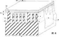
图4为图3装置的一替补方案,它消除了对上微结构的需要,如图4所见,一个或多个宏电极32(它们是毫米量级的平面结构)高出微电极6被支承在从衬底4向上伸出的弹性体脊16之上。采用有选择地移去衬底4和弹性体脊5的某些部分来制造出储气室24,操作时,将电势差施加于微电极6和宏电极32之间,以在它们之间产生一静电吸引力。这一静电吸引力使弹性体脊16产生变形,从而使微电极和宏电极相互间产生相对运动。在此运动期间,被围在空间20中的气体在宏电极和衬底4间被压缩。Fig. 4 is an alternative scheme of Fig. 3 device, and it has eliminated the need to upper microstructure, and as seen in Fig. 4, one or more macroelectrodes 32 (they are the planar structure of order of millimeters) higher than
图5A和5B示出一进一步的替补实施例,其中将一个或多个宏电极30加于衬底4的基底上。操作时,将一电势差加于微电极6和宏电极30之间,以在它们之间产生一静电吸引力。该静电吸引力使弹性体脊5变形,从而使微电极6如图5B所示的那样相对于宏电极30移动。5A and 5B show a further alternative embodiment in which one or more macroelectrodes 30 are added to the base of the
图6示出一更进一步的替补实施例,其中将微电极6和6’施加于衬底4的两侧。可看到这样便提供了上、下两结构(对称于衬底4的平面),每一结构以上述图1A-1D所示的方式工作。这样一种双边结构可被用于例如改善通过薄膜的对流热传递。Figure 6 shows a further alternative embodiment in which microelectrodes 6 and 6' are applied to both sides of the
根据前面披露的内容,熟悉本技术领域的人将可看到,在实施本发明过程中在不偏离本发明的精神和范围的条件下仍会有许多替代方案和修改。因此,有必要根据以下权利要求所述的精神来解释本发明的范围。From the foregoing disclosure, those skilled in the art will recognize that many alternatives and modifications can be practiced in the practice of the invention without departing from the spirit and scope of the invention. Therefore, it is necessary to interpret the scope of the present invention in terms of the spirit described in the following claims.
Claims (17)
Translated fromChineseApplications Claiming Priority (2)
| Application Number | Priority Date | Filing Date | Title |
|---|---|---|---|
| US08/431,735US5642015A (en) | 1993-07-14 | 1995-05-01 | Elastomeric micro electro mechanical systems |
| US08/431,735 | 1995-05-01 |
Publications (2)
| Publication Number | Publication Date |
|---|---|
| CN1186458Atrue CN1186458A (en) | 1998-07-01 |
| CN1047107C CN1047107C (en) | 1999-12-08 |
Family
ID=23713203
Family Applications (1)
| Application Number | Title | Priority Date | Filing Date |
|---|---|---|---|
| CN96194329AExpired - Fee RelatedCN1047107C (en) | 1995-05-01 | 1996-04-26 | Elastmeric micro electromechanical systems |
Country Status (9)
| Country | Link |
|---|---|
| US (1) | US5642015A (en) |
| EP (1) | EP0824381B1 (en) |
| JP (1) | JP3016870B2 (en) |
| KR (1) | KR100286486B1 (en) |
| CN (1) | CN1047107C (en) |
| AU (1) | AU5394596A (en) |
| CA (1) | CA2218876C (en) |
| DE (1) | DE69609414T2 (en) |
| WO (1) | WO1996034701A1 (en) |
Cited By (1)
| Publication number | Priority date | Publication date | Assignee | Title |
|---|---|---|---|---|
| CN101749888A (en)* | 2008-12-06 | 2010-06-23 | 托马斯·R·克雷尼科 | Air circulation heat pump technology and system |
Families Citing this family (183)
| Publication number | Priority date | Publication date | Assignee | Title |
|---|---|---|---|---|
| US6812624B1 (en)* | 1999-07-20 | 2004-11-02 | Sri International | Electroactive polymers |
| US6781284B1 (en) | 1997-02-07 | 2004-08-24 | Sri International | Electroactive polymer transducers and actuators |
| US7320457B2 (en)* | 1997-02-07 | 2008-01-22 | Sri International | Electroactive polymer devices for controlling fluid flow |
| US6376971B1 (en) | 1997-02-07 | 2002-04-23 | Sri International | Electroactive polymer electrodes |
| US6545384B1 (en) | 1997-02-07 | 2003-04-08 | Sri International | Electroactive polymer devices |
| US7214298B2 (en)* | 1997-09-23 | 2007-05-08 | California Institute Of Technology | Microfabricated cell sorter |
| US6833242B2 (en)* | 1997-09-23 | 2004-12-21 | California Institute Of Technology | Methods for detecting and sorting polynucleotides based on size |
| DE19825581A1 (en)* | 1998-06-09 | 1999-12-16 | Volkswagen Ag | Ultrasonic film transformer for measuring distance to another object, e.g. a vehicle, and manufacturing process giving a transformer which can be easily adapted to different contours |
| US6216973B1 (en) | 1998-10-23 | 2001-04-17 | Trw Vehicle Safety Systems Inc. | Electric locking seat belt retractor |
| US6184608B1 (en) | 1998-12-29 | 2001-02-06 | Honeywell International Inc. | Polymer microactuator array with macroscopic force and displacement |
| US6184607B1 (en)* | 1998-12-29 | 2001-02-06 | Honeywell International Inc. | Driving strategy for non-parallel arrays of electrostatic actuators sharing a common electrode |
| US6297069B1 (en) | 1999-01-28 | 2001-10-02 | Honeywell Inc. | Method for supporting during fabrication mechanical members of semi-conductive dies, wafers, and devices and an associated intermediate device assembly |
| MXPA01009999A (en)* | 1999-04-06 | 2003-07-14 | Uab Research Foundation | Method for screening crystallization conditions in solution crystal growth. |
| US7244396B2 (en)* | 1999-04-06 | 2007-07-17 | Uab Research Foundation | Method for preparation of microarrays for screening of crystal growth conditions |
| US7250305B2 (en)* | 2001-07-30 | 2007-07-31 | Uab Research Foundation | Use of dye to distinguish salt and protein crystals under microcrystallization conditions |
| US7247490B2 (en)* | 1999-04-06 | 2007-07-24 | Uab Research Foundation | Method for screening crystallization conditions in solution crystal growth |
| US20030022383A1 (en)* | 1999-04-06 | 2003-01-30 | Uab Research Foundation | Method for screening crystallization conditions in solution crystal growth |
| US7214540B2 (en) | 1999-04-06 | 2007-05-08 | Uab Research Foundation | Method for screening crystallization conditions in solution crystal growth |
| US6166478A (en)* | 1999-06-04 | 2000-12-26 | The Board Of Trustees Of The University Of Illinois | Method for assembly of microelectromechanical systems using magnetic actuation |
| US7195670B2 (en) | 2000-06-27 | 2007-03-27 | California Institute Of Technology | High throughput screening of crystallization of materials |
| DK1065378T3 (en)* | 1999-06-28 | 2002-07-29 | California Inst Of Techn | Elastomeric micropump and micro valve systems |
| US7459022B2 (en)* | 2001-04-06 | 2008-12-02 | California Institute Of Technology | Microfluidic protein crystallography |
| US20080277007A1 (en)* | 1999-06-28 | 2008-11-13 | California Institute Of Technology | Microfabricated elastomeric valve and pump systems |
| US7217321B2 (en)* | 2001-04-06 | 2007-05-15 | California Institute Of Technology | Microfluidic protein crystallography techniques |
| US8052792B2 (en)* | 2001-04-06 | 2011-11-08 | California Institute Of Technology | Microfluidic protein crystallography techniques |
| US6929030B2 (en)* | 1999-06-28 | 2005-08-16 | California Institute Of Technology | Microfabricated elastomeric valve and pump systems |
| US8550119B2 (en)* | 1999-06-28 | 2013-10-08 | California Institute Of Technology | Microfabricated elastomeric valve and pump systems |
| US6899137B2 (en)* | 1999-06-28 | 2005-05-31 | California Institute Of Technology | Microfabricated elastomeric valve and pump systems |
| US7144616B1 (en)* | 1999-06-28 | 2006-12-05 | California Institute Of Technology | Microfabricated elastomeric valve and pump systems |
| US7052545B2 (en)* | 2001-04-06 | 2006-05-30 | California Institute Of Technology | High throughput screening of crystallization of materials |
| US7306672B2 (en)* | 2001-04-06 | 2007-12-11 | California Institute Of Technology | Microfluidic free interface diffusion techniques |
| US7244402B2 (en)* | 2001-04-06 | 2007-07-17 | California Institute Of Technology | Microfluidic protein crystallography |
| US8709153B2 (en) | 1999-06-28 | 2014-04-29 | California Institute Of Technology | Microfludic protein crystallography techniques |
| US7537197B2 (en)* | 1999-07-20 | 2009-05-26 | Sri International | Electroactive polymer devices for controlling fluid flow |
| US6664718B2 (en) | 2000-02-09 | 2003-12-16 | Sri International | Monolithic electroactive polymers |
| DE60037433T2 (en)* | 1999-07-20 | 2008-12-04 | Sri International, Menlo Park | Electroactive polymer generators |
| FR2803957B1 (en)* | 2000-01-13 | 2002-03-08 | Information Technology Dev | CAPACITIVE MICRO ACTUATOR WITH OPTIMIZED DEFORMABLE STRUCTURE FOR DISK MEMORY AND MANUFACTURING METHOD |
| US6753638B2 (en)* | 2000-02-03 | 2004-06-22 | Calient Networks, Inc. | Electrostatic actuator for micromechanical systems |
| US6911764B2 (en) | 2000-02-09 | 2005-06-28 | Sri International | Energy efficient electroactive polymers and electroactive polymer devices |
| AU2001238459A1 (en)* | 2000-02-16 | 2001-08-27 | Omlidon Technologies Llc | Method for microstructuring polymer-supported materials |
| WO2001065615A2 (en)* | 2000-02-23 | 2001-09-07 | Sri International | Biologically powered electroactive polymer generators |
| WO2001063738A2 (en)* | 2000-02-23 | 2001-08-30 | Sri International | Electroactive polymer thermal electric generators |
| AU2001240040A1 (en)* | 2000-03-03 | 2001-09-17 | California Institute Of Technology | Combinatorial array for nucleic acid analysis |
| DE60122517T2 (en) | 2000-03-31 | 2007-03-08 | Lifescan, Inc., Milpitas | ELECTRICALLY CONDUCTIVE PATTERN FOR MONITORING THE FILLING OF MEDICAL DEVICES |
| US20050118073A1 (en)* | 2003-11-26 | 2005-06-02 | Fluidigm Corporation | Devices and methods for holding microfluidic devices |
| US7279146B2 (en)* | 2003-04-17 | 2007-10-09 | Fluidigm Corporation | Crystal growth devices and systems, and methods for using same |
| US8105553B2 (en)* | 2004-01-25 | 2012-01-31 | Fluidigm Corporation | Crystal forming devices and systems and methods for using the same |
| US7867763B2 (en)* | 2004-01-25 | 2011-01-11 | Fluidigm Corporation | Integrated chip carriers with thermocycler interfaces and methods of using the same |
| US6628041B2 (en)* | 2000-05-16 | 2003-09-30 | Calient Networks, Inc. | Micro-electro-mechanical-system (MEMS) mirror device having large angle out of plane motion using shaped combed finger actuators and method for fabricating the same |
| US7420659B1 (en)* | 2000-06-02 | 2008-09-02 | Honeywell Interantional Inc. | Flow control system of a cartridge |
| US6837476B2 (en) | 2002-06-19 | 2005-01-04 | Honeywell International Inc. | Electrostatically actuated valve |
| US6568286B1 (en) | 2000-06-02 | 2003-05-27 | Honeywell International Inc. | 3D array of integrated cells for the sampling and detection of air bound chemical and biological species |
| US7351376B1 (en) | 2000-06-05 | 2008-04-01 | California Institute Of Technology | Integrated active flux microfluidic devices and methods |
| US6829753B2 (en)* | 2000-06-27 | 2004-12-07 | Fluidigm Corporation | Microfluidic design automation method and system |
| US7000330B2 (en)* | 2002-08-21 | 2006-02-21 | Honeywell International Inc. | Method and apparatus for receiving a removable media member |
| AU2001278697A1 (en)* | 2000-08-11 | 2002-02-25 | Ecchandes Inc. | Overlapping type piezoelectric stator, overlapping type piezoelectric acturator and applications thereof |
| WO2002023163A1 (en)* | 2000-09-15 | 2002-03-21 | California Institute Of Technology | Microfabricated crossflow devices and methods |
| US6842964B1 (en) | 2000-09-29 | 2005-01-18 | Tucker Davis Technologies, Inc. | Process of manufacturing of electrostatic speakers |
| US6825967B1 (en) | 2000-09-29 | 2004-11-30 | Calient Networks, Inc. | Shaped electrodes for micro-electro-mechanical-system (MEMS) devices to improve actuator performance and methods for fabricating the same |
| EP1322936A2 (en)* | 2000-10-03 | 2003-07-02 | California Institute Of Technology | Microfluidic devices and methods of use |
| US7097809B2 (en)* | 2000-10-03 | 2006-08-29 | California Institute Of Technology | Combinatorial synthesis system |
| US7678547B2 (en)* | 2000-10-03 | 2010-03-16 | California Institute Of Technology | Velocity independent analyte characterization |
| AU1189702A (en)* | 2000-10-13 | 2002-04-22 | Fluidigm Corp | Microfluidic device based sample injection system for analytical devices |
| US7548015B2 (en)* | 2000-11-02 | 2009-06-16 | Danfoss A/S | Multilayer composite and a method of making such |
| US7518284B2 (en) | 2000-11-02 | 2009-04-14 | Danfoss A/S | Dielectric composite and a method of manufacturing a dielectric composite |
| DE10054247C2 (en) | 2000-11-02 | 2002-10-24 | Danfoss As | Actuator and method for its manufacture |
| US8181338B2 (en) | 2000-11-02 | 2012-05-22 | Danfoss A/S | Method of making a multilayer composite |
| US7232109B2 (en)* | 2000-11-06 | 2007-06-19 | California Institute Of Technology | Electrostatic valves for microfluidic devices |
| AU2002248149A1 (en)* | 2000-11-16 | 2002-08-12 | Fluidigm Corporation | Microfluidic devices for introducing and dispensing fluids from microfluidic systems |
| AU2002230524A1 (en) | 2000-11-16 | 2002-05-27 | California Institute Of Technology | Apparatus and methods for conducting assays and high throughput screening |
| US20050196785A1 (en)* | 2001-03-05 | 2005-09-08 | California Institute Of Technology | Combinational array for nucleic acid analysis |
| US7670429B2 (en)* | 2001-04-05 | 2010-03-02 | The California Institute Of Technology | High throughput screening of crystallization of materials |
| AU2002307152A1 (en) | 2001-04-06 | 2002-10-21 | California Institute Of Technology | Nucleic acid amplification utilizing microfluidic devices |
| US6752922B2 (en)* | 2001-04-06 | 2004-06-22 | Fluidigm Corporation | Microfluidic chromatography |
| JP5162074B2 (en) | 2001-04-06 | 2013-03-13 | フルイディグム コーポレイション | Polymer surface modification |
| US6802342B2 (en)* | 2001-04-06 | 2004-10-12 | Fluidigm Corporation | Microfabricated fluidic circuit elements and applications |
| US20020164816A1 (en)* | 2001-04-06 | 2002-11-07 | California Institute Of Technology | Microfluidic sample separation device |
| US7233097B2 (en)* | 2001-05-22 | 2007-06-19 | Sri International | Rolled electroactive polymers |
| US6543087B2 (en) | 2001-06-01 | 2003-04-08 | Aip Networks, Inc. | Micro-electromechanical hinged flap structure |
| US20050149304A1 (en)* | 2001-06-27 | 2005-07-07 | Fluidigm Corporation | Object oriented microfluidic design method and system |
| US7075162B2 (en)* | 2001-08-30 | 2006-07-11 | Fluidigm Corporation | Electrostatic/electrostrictive actuation of elastomer structures using compliant electrodes |
| US6729856B2 (en) | 2001-10-09 | 2004-05-04 | Honeywell International Inc. | Electrostatically actuated pump with elastic restoring forces |
| US7192629B2 (en) | 2001-10-11 | 2007-03-20 | California Institute Of Technology | Devices utilizing self-assembled gel and method of manufacture |
| US8440093B1 (en) | 2001-10-26 | 2013-05-14 | Fuidigm Corporation | Methods and devices for electronic and magnetic sensing of the contents of microfluidic flow channels |
| US7064740B2 (en)* | 2001-11-09 | 2006-06-20 | Sharp Laboratories Of America, Inc. | Backlit display with improved dynamic range |
| JP4355210B2 (en) | 2001-11-30 | 2009-10-28 | フルイディグム コーポレイション | Microfluidic device and method of using microfluidic device |
| US7691333B2 (en)* | 2001-11-30 | 2010-04-06 | Fluidigm Corporation | Microfluidic device and methods of using same |
| DE60224844T2 (en) | 2001-12-21 | 2009-01-08 | Danfoss A/S | DIELECTRIC ACTUATOR OR SENSOR STRUCTURE AND MANUFACTURING METHOD |
| AU2003225913A1 (en)* | 2002-03-18 | 2003-10-08 | Roy David Kornbluh | Electroactive polymer devices for moving fluid |
| WO2003085379A2 (en) | 2002-04-01 | 2003-10-16 | Fluidigm Corporation | Microfluidic particle-analysis systems |
| US7312085B2 (en) | 2002-04-01 | 2007-12-25 | Fluidigm Corporation | Microfluidic particle-analysis systems |
| US20070026528A1 (en)* | 2002-05-30 | 2007-02-01 | Delucas Lawrence J | Method for screening crystallization conditions in solution crystal growth |
| EP1535296A4 (en)* | 2002-06-14 | 2007-04-04 | Ibm | Micro-electromechanical switch having a deformable elastomeric conductive element |
| AU2003256469A1 (en)* | 2002-07-10 | 2004-01-23 | Uab Research Foundation | Method for distinguishing between biomolecule and non-biomolecule crystals |
| EP1540807B1 (en)* | 2002-09-20 | 2013-01-09 | Danfoss A/S | Elastomer actuator and method of making the actuator |
| US8220494B2 (en)* | 2002-09-25 | 2012-07-17 | California Institute Of Technology | Microfluidic large scale integration |
| JP2006501056A (en)* | 2002-09-25 | 2006-01-12 | カリフォルニア インスティテュート オブ テクノロジー | Micro fluid large scale integration |
| EP1546412B1 (en) | 2002-10-02 | 2014-05-21 | California Institute Of Technology | Microfluidic nucleic acid analysis |
| ATE440319T1 (en)* | 2002-12-12 | 2009-09-15 | Danfoss As | TOUCH SENSOR ELEMENT AND SENSOR GROUP |
| US7868221B2 (en) | 2003-02-24 | 2011-01-11 | Danfoss A/S | Electro active elastic compression bandage |
| US7476363B2 (en)* | 2003-04-03 | 2009-01-13 | Fluidigm Corporation | Microfluidic devices and methods of using same |
| US7604965B2 (en) | 2003-04-03 | 2009-10-20 | Fluidigm Corporation | Thermal reaction device and method for using the same |
| US8828663B2 (en) | 2005-03-18 | 2014-09-09 | Fluidigm Corporation | Thermal reaction device and method for using the same |
| US7666361B2 (en)* | 2003-04-03 | 2010-02-23 | Fluidigm Corporation | Microfluidic devices and methods of using same |
| US20050145496A1 (en)* | 2003-04-03 | 2005-07-07 | Federico Goodsaid | Thermal reaction device and method for using the same |
| CA2526368A1 (en) | 2003-05-20 | 2004-12-02 | Fluidigm Corporation | Method and system for microfluidic device and imaging thereof |
| EP1667829A4 (en)* | 2003-07-28 | 2008-12-10 | Fluidigm Corp | IMAGE PROCESSING METHOD AND SYSTEM FOR MICROFLUIDIC DEVICES |
| US7413712B2 (en) | 2003-08-11 | 2008-08-19 | California Institute Of Technology | Microfluidic rotary flow reactor matrix |
| WO2005052673A2 (en) | 2003-11-21 | 2005-06-09 | Sharp Laboratories Of America, Inc. | Liquid crystal display with adaptive color |
| KR100875326B1 (en)* | 2003-12-18 | 2008-12-22 | 샤프 가부시키가이샤 | Liquid crystal display response characteristics determination method and presentation method |
| US7407799B2 (en)* | 2004-01-16 | 2008-08-05 | California Institute Of Technology | Microfluidic chemostat |
| US7505018B2 (en) | 2004-05-04 | 2009-03-17 | Sharp Laboratories Of America, Inc. | Liquid crystal display with reduced black level insertion |
| US7532192B2 (en) | 2004-05-04 | 2009-05-12 | Sharp Laboratories Of America, Inc. | Liquid crystal display with filtered black point |
| US7777714B2 (en) | 2004-05-04 | 2010-08-17 | Sharp Laboratories Of America, Inc. | Liquid crystal display with adaptive width |
| US7872631B2 (en) | 2004-05-04 | 2011-01-18 | Sharp Laboratories Of America, Inc. | Liquid crystal display with temporal black point |
| US7602369B2 (en)* | 2004-05-04 | 2009-10-13 | Sharp Laboratories Of America, Inc. | Liquid crystal display with colored backlight |
| US8395577B2 (en) | 2004-05-04 | 2013-03-12 | Sharp Laboratories Of America, Inc. | Liquid crystal display with illumination control |
| US7612757B2 (en) | 2004-05-04 | 2009-11-03 | Sharp Laboratories Of America, Inc. | Liquid crystal display with modulated black point |
| US20060024751A1 (en)* | 2004-06-03 | 2006-02-02 | Fluidigm Corporation | Scale-up methods and systems for performing the same |
| US7023451B2 (en)* | 2004-06-14 | 2006-04-04 | Sharp Laboratories Of America, Inc. | System for reducing crosstalk |
| US7116463B2 (en)* | 2004-07-15 | 2006-10-03 | Optron Systems, Inc. | High angular deflection micro-mirror system |
| US7556836B2 (en) | 2004-09-03 | 2009-07-07 | Solae, Llc | High protein snack product |
| US7898519B2 (en) | 2005-02-17 | 2011-03-01 | Sharp Laboratories Of America, Inc. | Method for overdriving a backlit display |
| US8050512B2 (en) | 2004-11-16 | 2011-11-01 | Sharp Laboratories Of America, Inc. | High dynamic range images from low dynamic range images |
| US8050511B2 (en) | 2004-11-16 | 2011-11-01 | Sharp Laboratories Of America, Inc. | High dynamic range images from low dynamic range images |
| US7525528B2 (en) | 2004-11-16 | 2009-04-28 | Sharp Laboratories Of America, Inc. | Technique that preserves specular highlights |
| US20060134510A1 (en)* | 2004-12-21 | 2006-06-22 | Cleopatra Cabuz | Air cell air flow control system and method |
| US7222639B2 (en)* | 2004-12-29 | 2007-05-29 | Honeywell International Inc. | Electrostatically actuated gas valve |
| US7328882B2 (en)* | 2005-01-06 | 2008-02-12 | Honeywell International Inc. | Microfluidic modulating valve |
| US7445017B2 (en)* | 2005-01-28 | 2008-11-04 | Honeywell International Inc. | Mesovalve modulator |
| US7320338B2 (en)* | 2005-06-03 | 2008-01-22 | Honeywell International Inc. | Microvalve package assembly |
| US7517201B2 (en)* | 2005-07-14 | 2009-04-14 | Honeywell International Inc. | Asymmetric dual diaphragm pump |
| US20070051415A1 (en)* | 2005-09-07 | 2007-03-08 | Honeywell International Inc. | Microvalve switching array |
| US7624755B2 (en) | 2005-12-09 | 2009-12-01 | Honeywell International Inc. | Gas valve with overtravel |
| US8121401B2 (en) | 2006-01-24 | 2012-02-21 | Sharp Labortories of America, Inc. | Method for reducing enhancement of artifacts and noise in image color enhancement |
| US9143657B2 (en) | 2006-01-24 | 2015-09-22 | Sharp Laboratories Of America, Inc. | Color enhancement technique using skin color detection |
| US7815868B1 (en) | 2006-02-28 | 2010-10-19 | Fluidigm Corporation | Microfluidic reaction apparatus for high throughput screening |
| US7523762B2 (en) | 2006-03-22 | 2009-04-28 | Honeywell International Inc. | Modulating gas valves and systems |
| US8007704B2 (en)* | 2006-07-20 | 2011-08-30 | Honeywell International Inc. | Insert molded actuator components |
| US7543604B2 (en)* | 2006-09-11 | 2009-06-09 | Honeywell International Inc. | Control valve |
| US7732999B2 (en)* | 2006-11-03 | 2010-06-08 | Danfoss A/S | Direct acting capacitive transducer |
| US7880371B2 (en) | 2006-11-03 | 2011-02-01 | Danfoss A/S | Dielectric composite and a method of manufacturing a dielectric composite |
| US8941580B2 (en) | 2006-11-30 | 2015-01-27 | Sharp Laboratories Of America, Inc. | Liquid crystal display with area adaptive backlight |
| US7644731B2 (en) | 2006-11-30 | 2010-01-12 | Honeywell International Inc. | Gas valve with resilient seat |
| EP1970122A1 (en)* | 2007-03-12 | 2008-09-17 | Koninklijke Philips Electronics N.V. | Microfluidic system based on magnetic actuator elements |
| US7952261B2 (en) | 2007-06-29 | 2011-05-31 | Bayer Materialscience Ag | Electroactive polymer transducers for sensory feedback applications |
| EP2283265A2 (en)* | 2008-04-30 | 2011-02-16 | Danfoss Polypower A/S | A power actuated valve |
| WO2009132651A1 (en)* | 2008-04-30 | 2009-11-05 | Danfoss A/S | A pump powered by a polymer transducer |
| EP2239793A1 (en) | 2009-04-11 | 2010-10-13 | Bayer MaterialScience AG | Electrically switchable polymer film structure and use thereof |
| US8712559B2 (en)* | 2010-02-10 | 2014-04-29 | The Board Of Trustees Of The University Of Illionois | Adaptive control for uncertain nonlinear multi-input multi-output systems |
| JP5548563B2 (en)* | 2010-09-14 | 2014-07-16 | ヤマハ株式会社 | Nanosheet transducer |
| US9553254B2 (en) | 2011-03-01 | 2017-01-24 | Parker-Hannifin Corporation | Automated manufacturing processes for producing deformable polymer devices and films |
| EP2689284A4 (en) | 2011-03-22 | 2014-08-20 | Bayer Ip Gmbh | Electroactive polymer actuator lenticular system |
| US9835265B2 (en) | 2011-12-15 | 2017-12-05 | Honeywell International Inc. | Valve with actuator diagnostics |
| US8899264B2 (en) | 2011-12-15 | 2014-12-02 | Honeywell International Inc. | Gas valve with electronic proof of closure system |
| US8947242B2 (en) | 2011-12-15 | 2015-02-03 | Honeywell International Inc. | Gas valve with valve leakage test |
| US9851103B2 (en) | 2011-12-15 | 2017-12-26 | Honeywell International Inc. | Gas valve with overpressure diagnostics |
| US8905063B2 (en) | 2011-12-15 | 2014-12-09 | Honeywell International Inc. | Gas valve with fuel rate monitor |
| US8839815B2 (en) | 2011-12-15 | 2014-09-23 | Honeywell International Inc. | Gas valve with electronic cycle counter |
| US9846440B2 (en) | 2011-12-15 | 2017-12-19 | Honeywell International Inc. | Valve controller configured to estimate fuel comsumption |
| US9995486B2 (en) | 2011-12-15 | 2018-06-12 | Honeywell International Inc. | Gas valve with high/low gas pressure detection |
| US9074770B2 (en) | 2011-12-15 | 2015-07-07 | Honeywell International Inc. | Gas valve with electronic valve proving system |
| US9557059B2 (en) | 2011-12-15 | 2017-01-31 | Honeywell International Inc | Gas valve with communication link |
| US8891222B2 (en) | 2012-02-14 | 2014-11-18 | Danfoss A/S | Capacitive transducer and a method for manufacturing a transducer |
| US8692442B2 (en) | 2012-02-14 | 2014-04-08 | Danfoss Polypower A/S | Polymer transducer and a connector for a transducer |
| EP2828901B1 (en) | 2012-03-21 | 2017-01-04 | Parker Hannifin Corporation | Roll-to-roll manufacturing processes for producing self-healing electroactive polymer devices |
| US9761790B2 (en) | 2012-06-18 | 2017-09-12 | Parker-Hannifin Corporation | Stretch frame for stretching process |
| US9234661B2 (en) | 2012-09-15 | 2016-01-12 | Honeywell International Inc. | Burner control system |
| US10422531B2 (en) | 2012-09-15 | 2019-09-24 | Honeywell International Inc. | System and approach for controlling a combustion chamber |
| WO2014066576A1 (en) | 2012-10-24 | 2014-05-01 | Bayer Intellectual Property Gmbh | Polymer diode |
| WO2014117724A1 (en)* | 2013-01-29 | 2014-08-07 | 中国科学院苏州纳米技术与纳米仿生研究所 | Electronic skin, preparation method and use thereof |
| EP2868970B1 (en) | 2013-10-29 | 2020-04-22 | Honeywell Technologies Sarl | Regulating device |
| US10024439B2 (en) | 2013-12-16 | 2018-07-17 | Honeywell International Inc. | Valve over-travel mechanism |
| US9841122B2 (en) | 2014-09-09 | 2017-12-12 | Honeywell International Inc. | Gas valve with electronic valve proving system |
| US9645584B2 (en) | 2014-09-17 | 2017-05-09 | Honeywell International Inc. | Gas valve with electronic health monitoring |
| US9899937B2 (en)* | 2015-01-16 | 2018-02-20 | Wisconsin Alumni Research Foundation | Peg-style electrostatic rotating machine |
| US10503181B2 (en) | 2016-01-13 | 2019-12-10 | Honeywell International Inc. | Pressure regulator |
| US10564062B2 (en) | 2016-10-19 | 2020-02-18 | Honeywell International Inc. | Human-machine interface for gas valve |
| US11073281B2 (en) | 2017-12-29 | 2021-07-27 | Honeywell International Inc. | Closed-loop programming and control of a combustion appliance |
| US10697815B2 (en) | 2018-06-09 | 2020-06-30 | Honeywell International Inc. | System and methods for mitigating condensation in a sensor module |
| WO2020097730A1 (en)* | 2018-11-16 | 2020-05-22 | The University Of British Columbia | Deformable sensor for simulating skin and other applications |
| US11713240B2 (en)* | 2019-12-09 | 2023-08-01 | Board Of Regents, The University Of Texas System | Cellular array electrostatic actuator |
| US12103843B2 (en) | 2021-01-20 | 2024-10-01 | Calient.Ai Inc. | MEMS mirror arrays with reduced crosstalk |
Family Cites Families (11)
| Publication number | Priority date | Publication date | Assignee | Title |
|---|---|---|---|---|
| US3772537A (en)* | 1972-10-27 | 1973-11-13 | Trw Inc | Electrostatically actuated device |
| US4376302A (en)* | 1978-04-13 | 1983-03-08 | The United States Of America As Represented By The Secretary Of The Navy | Piezoelectric polymer hydrophone |
| US4654546A (en)* | 1984-11-20 | 1987-03-31 | Kari Kirjavainen | Electromechanical film and procedure for manufacturing same |
| CA1277415C (en)* | 1986-04-11 | 1990-12-04 | Lorne A. Whitehead | Elastomer membrane enhanced electrostatic transducer |
| US4887248A (en)* | 1988-07-07 | 1989-12-12 | Cleveland Machine Controls, Inc. | Electrostatic transducer and method of making and using same |
| JP2797146B2 (en)* | 1990-10-09 | 1998-09-17 | 株式会社ゼクセル | Electromagnetic actuator for moving objects |
| US5206557A (en)* | 1990-11-27 | 1993-04-27 | Mcnc | Microelectromechanical transducer and fabrication method |
| US5485437A (en)* | 1993-02-05 | 1996-01-16 | Discovision Associates | Shock-resistant, electrostatically actuated pick-up for optical recording and playback |
| US5450498A (en) | 1993-07-14 | 1995-09-12 | The University Of British Columbia | High pressure low impedance electrostatic transducer |
| US5359574A (en)* | 1993-08-27 | 1994-10-25 | The United States Of America As Represented By The Secretary Of The Navy | Electromagnetically activated compliant wavy-wall |
| US5395592A (en)* | 1993-10-04 | 1995-03-07 | Bolleman; Brent | Acoustic liquid processing device |
- 1995
- 1995-05-01USUS08/431,735patent/US5642015A/ennot_activeExpired - Fee Related
- 1996
- 1996-04-26KRKR1019970707737Apatent/KR100286486B1/ennot_activeExpired - Fee Related
- 1996-04-26EPEP96910876Apatent/EP0824381B1/ennot_activeExpired - Lifetime
- 1996-04-26CACA002218876Apatent/CA2218876C/ennot_activeExpired - Fee Related
- 1996-04-26DEDE69609414Tpatent/DE69609414T2/ennot_activeExpired - Fee Related
- 1996-04-26CNCN96194329Apatent/CN1047107C/ennot_activeExpired - Fee Related
- 1996-04-26AUAU53945/96Apatent/AU5394596A/ennot_activeAbandoned
- 1996-04-26JPJP8532877Apatent/JP3016870B2/ennot_activeExpired - Fee Related
- 1996-04-26WOPCT/CA1996/000268patent/WO1996034701A1/enactiveIP Right Grant
Cited By (1)
| Publication number | Priority date | Publication date | Assignee | Title |
|---|---|---|---|---|
| CN101749888A (en)* | 2008-12-06 | 2010-06-23 | 托马斯·R·克雷尼科 | Air circulation heat pump technology and system |
Also Published As
| Publication number | Publication date |
|---|---|
| AU5394596A (en) | 1996-11-21 |
| KR19990008212A (en) | 1999-01-25 |
| CA2218876C (en) | 1999-12-07 |
| JP3016870B2 (en) | 2000-03-06 |
| JPH10511528A (en) | 1998-11-04 |
| DE69609414T2 (en) | 2001-03-08 |
| CN1047107C (en) | 1999-12-08 |
| MX9708359A (en) | 1998-06-30 |
| CA2218876A1 (en) | 1996-11-07 |
| KR100286486B1 (en) | 2001-04-16 |
| EP0824381A1 (en) | 1998-02-25 |
| WO1996034701A1 (en) | 1996-11-07 |
| DE69609414D1 (en) | 2000-08-24 |
| US5642015A (en) | 1997-06-24 |
| EP0824381B1 (en) | 2000-07-19 |
Similar Documents
| Publication | Publication Date | Title |
|---|---|---|
| CN1186458A (en) | Elastomeric MEMS | |
| US11616455B2 (en) | Electrostatic actuator | |
| US6583533B2 (en) | Electroactive polymer electrodes | |
| US6543110B1 (en) | Electroactive polymer fabrication | |
| US6940211B2 (en) | Electroactive polymers transducers and actuators | |
| EP1848046B1 (en) | Transducers of electroactive polymers | |
| EP1145417B1 (en) | Polymer microactuator array with macroscopic force and displacement | |
| US10804818B2 (en) | Triboelectric generator and network for mechanical energy harvesting | |
| WO1997036366A1 (en) | Piezoelectric actuator or motor, method therefor and method for fabrication thereof | |
| RU98119708A (en) | PIEZOELECTRIC DRIVE OR ENGINE, METHOD FOR PUTING IT INTO ACTION AND METHOD FOR PRODUCING IT | |
| JP2004516783A (en) | Electrostatic device | |
| JPH05219760A (en) | Electrostatic actuator | |
| US7705514B2 (en) | Bi-directional actuator utilizing both attractive and repulsive electrostatic forces | |
| JP2007259663A (en) | Stacked electrostatic actuator | |
| WO2017092829A1 (en) | Electro-active loudspeaker | |
| CN1188340C (en) | Electrostatic actuating micro-holder | |
| US20050067919A1 (en) | Polymer actuator having a circular unit cell | |
| MXPA97008359A (en) | Elastomeri microelectromecanic system | |
| US11713240B2 (en) | Cellular array electrostatic actuator | |
| Pelrine et al. | Artificial muscle for small robots and other micromechanical devices | |
| Tominaga et al. | A bending and expanding motion actuator | |
| Niino et al. | Dual excitation electrostatic stepping motor | |
| Tominaga et al. | A bending and expanding motion actuator | |
| Vanagas et al. | Asymmetric Cmut Cells as Building Blocks of the System-on-Chip Microfluidic Valves |
Legal Events
| Date | Code | Title | Description |
|---|---|---|---|
| C06 | Publication | ||
| PB01 | Publication | ||
| C10 | Entry into substantive examination | ||
| SE01 | Entry into force of request for substantive examination | ||
| C14 | Grant of patent or utility model | ||
| GR01 | Patent grant | ||
| C19 | Lapse of patent right due to non-payment of the annual fee | ||
| CF01 | Termination of patent right due to non-payment of annual fee |