CN1185685C - Thin film transistor liquid crystal display and manufacturing method thereof - Google Patents
Thin film transistor liquid crystal display and manufacturing method thereofDownload PDFInfo
- Publication number
- CN1185685C CN1185685CCNB011406941ACN01140694ACN1185685CCN 1185685 CCN1185685 CCN 1185685CCN B011406941 ACNB011406941 ACN B011406941ACN 01140694 ACN01140694 ACN 01140694ACN 1185685 CCN1185685 CCN 1185685C
- Authority
- CN
- China
- Prior art keywords
- layer
- thin film
- film transistor
- manufacturing
- conductor
- Prior art date
- Legal status (The legal status is an assumption and is not a legal conclusion. Google has not performed a legal analysis and makes no representation as to the accuracy of the status listed.)
- Expired - Lifetime
Links
- 239000010409thin filmSubstances0.000titleclaimsabstractdescription46
- 238000004519manufacturing processMethods0.000titleclaimsabstractdescription35
- 239000004973liquid crystal related substanceSubstances0.000titleclaimsabstractdescription32
- 239000004020conductorSubstances0.000claimsabstractdescription72
- 239000000758substrateSubstances0.000claimsabstractdescription33
- 238000005530etchingMethods0.000claimsabstractdescription15
- 239000004065semiconductorSubstances0.000claimsdescription17
- 238000000034methodMethods0.000claimsdescription8
- 229910052751metalInorganic materials0.000claimsdescription6
- 239000002184metalSubstances0.000claimsdescription6
- 239000000463materialSubstances0.000claimsdescription4
- 239000007769metal materialSubstances0.000claimsdescription3
- 239000010410layerSubstances0.000description59
- 238000001459lithographyMethods0.000description11
- 239000011347resinSubstances0.000description8
- 229920005989resinPolymers0.000description8
- 238000000149argon plasma sinteringMethods0.000description6
- 238000010586diagramMethods0.000description5
- QTBSBXVTEAMEQO-UHFFFAOYSA-NAcetic acidChemical compoundCC(O)=OQTBSBXVTEAMEQO-UHFFFAOYSA-N0.000description3
- 229910052782aluminiumInorganic materials0.000description3
- XAGFODPZIPBFFR-UHFFFAOYSA-NaluminiumChemical compound[Al]XAGFODPZIPBFFR-UHFFFAOYSA-N0.000description3
- 229910021417amorphous siliconInorganic materials0.000description3
- 230000000694effectsEffects0.000description3
- AMGQUBHHOARCQH-UHFFFAOYSA-Nindium;oxotinChemical compound[In].[Sn]=OAMGQUBHHOARCQH-UHFFFAOYSA-N0.000description3
- 230000000149penetrating effectEffects0.000description3
- VYZAMTAEIAYCRO-UHFFFAOYSA-NChromiumChemical compound[Cr]VYZAMTAEIAYCRO-UHFFFAOYSA-N0.000description2
- RYGMFSIKBFXOCR-UHFFFAOYSA-NCopperChemical compound[Cu]RYGMFSIKBFXOCR-UHFFFAOYSA-N0.000description2
- NBIIXXVUZAFLBC-UHFFFAOYSA-NPhosphoric acidChemical compoundOP(O)(O)=ONBIIXXVUZAFLBC-UHFFFAOYSA-N0.000description2
- 229910052581Si3N4Inorganic materials0.000description2
- 229910052804chromiumInorganic materials0.000description2
- 239000011651chromiumSubstances0.000description2
- 229910052802copperInorganic materials0.000description2
- 239000010949copperSubstances0.000description2
- 230000008021depositionEffects0.000description2
- 230000005685electric field effectEffects0.000description2
- MGRWKWACZDFZJT-UHFFFAOYSA-Nmolybdenum tungstenChemical compound[Mo].[W]MGRWKWACZDFZJT-UHFFFAOYSA-N0.000description2
- 239000012508resin beadSubstances0.000description2
- HQVNEWCFYHHQES-UHFFFAOYSA-Nsilicon nitrideChemical compoundN12[Si]34N5[Si]62N3[Si]51N64HQVNEWCFYHHQES-UHFFFAOYSA-N0.000description2
- 229910052715tantalumInorganic materials0.000description2
- GUVRBAGPIYLISA-UHFFFAOYSA-Ntantalum atomChemical compound[Ta]GUVRBAGPIYLISA-UHFFFAOYSA-N0.000description2
- 229910002070thin film alloyInorganic materials0.000description2
- GRYLNZFGIOXLOG-UHFFFAOYSA-NNitric acidChemical compoundO[N+]([O-])=OGRYLNZFGIOXLOG-UHFFFAOYSA-N0.000description1
- XUIMIQQOPSSXEZ-UHFFFAOYSA-NSiliconChemical compound[Si]XUIMIQQOPSSXEZ-UHFFFAOYSA-N0.000description1
- 239000002253acidSubstances0.000description1
- 150000007513acidsChemical class0.000description1
- 229910000147aluminium phosphateInorganic materials0.000description1
- 230000015572biosynthetic processEffects0.000description1
- 239000003795chemical substances by applicationSubstances0.000description1
- VNTLIPZTSJSULJ-UHFFFAOYSA-Nchromium molybdenumChemical compound[Cr].[Mo]VNTLIPZTSJSULJ-UHFFFAOYSA-N0.000description1
- 229910021419crystalline siliconInorganic materials0.000description1
- 230000007812deficiencyEffects0.000description1
- 230000005684electric fieldEffects0.000description1
- 239000010408filmSubstances0.000description1
- 125000000896monocarboxylic acid groupChemical group0.000description1
- 229910017604nitric acidInorganic materials0.000description1
- 239000011241protective layerSubstances0.000description1
- 229910052710siliconInorganic materials0.000description1
- 239000010703siliconSubstances0.000description1
Images


Landscapes
- Liquid Crystal (AREA)
- Thin Film Transistor (AREA)
Abstract
Description
Translated fromChinese技术领域technical field
本发明涉及一种薄膜晶体管液晶显示器及其制造方法,尤指一种反射式或半穿透式式薄膜晶体管液晶显示器。The invention relates to a thin film transistor liquid crystal display and a manufacturing method thereof, in particular to a reflective or semi-transmissive thin film transistor liquid crystal display.
背景技术Background technique
随着制造技术的日益进展,液晶显示器(Liquid Crystal Display,LCD)已经是一种被广泛应用的显示组件,而其工作原理主要利用电场来控制液晶分子的排列状态,借由光线可通过液晶分子与否以实现屏幕上明暗的显示效果。因此,对于液晶显示器来说,如何有效获得较明亮的显示效果,实为一重要的研究目标。With the increasing progress of manufacturing technology, liquid crystal display (Liquid Crystal Display, LCD) has been a widely used display component, and its working principle mainly uses electric field to control the alignment state of liquid crystal molecules, and light can pass through liquid crystal molecules or not to achieve a bright and dark display effect on the screen. Therefore, for liquid crystal displays, how to effectively obtain a brighter display effect is an important research goal.
对于反射式或穿透反射式薄膜晶体管液晶显示器而言,由于其亮度是由光源的入射光及其反射光所决定,因此若要获得较明亮的显示效果,则必须增加光在垂直于屏幕方向的光散射强度。为达到上述目的,势必加强反射特性,于是便有在一第一透明电极板111上形成包含有数个具穿透性的树脂珠粒113的一树脂层114,如图1(a)所示,以使一光线透过所述彩色滤光片112及所述第一透明电极板111后而进入所述树脂层114时,借由所述数个具有穿透性的树脂珠粒113而使所述光线因碰撞而产生偏移,且经由薄膜晶体管的数组基板115上的第二透明电极板116及第一透明电极板间的电场效应使液晶分子产生光的散射,并透过反射板117将散射光反射出去。其优点是可以增加光散射角度,以间接控制光反射方向,但缺点是很难借由调整数个具穿透性的小球114位置以达到准确控制散射方向的目的。For reflective or transflective thin film transistor liquid crystal displays, since its brightness is determined by the incident light of the light source and its reflected light, in order to obtain a brighter display effect, it is necessary to increase the brightness of the light in the direction perpendicular to the screen. light scattering intensity. In order to achieve the above-mentioned purpose, it is necessary to strengthen the reflective properties, so a resin layer 114 comprising several penetrating resin beads 113 is formed on a first transparent electrode plate 111, as shown in Figure 1(a), When a light ray enters the resin layer 114 after passing through the color filter 112 and the first transparent electrode plate 111 , it is made possible by the several penetrating resin beads 113 . The light is deflected due to the collision, and the electric field effect between the second transparent electrode plate 116 and the first transparent electrode plate on the array substrate 115 of the thin film transistor causes the liquid crystal molecules to scatter light, and transmits light through the reflector 117 Scattered light is reflected. The advantage is that the light scattering angle can be increased to indirectly control the light reflection direction, but the disadvantage is that it is difficult to accurately control the scattering direction by adjusting the positions of several penetrating small balls 114 .
针对以上的缺失,后来还有直接在薄膜晶体管的数组基板125的第二透明电极板126上成长一树脂层124的制造,如图1(b)所示,当光线透过所述彩色滤光片122时,经由第二透明电极板126及第一透明电极板121间的电场效应使液晶分子产生光的散射,再由所述树脂层124将所述散射光反射出来,因所述树脂层124为一曲状结构,其不平整的表面可用以控制反射角度的大小,因此可有效控制光反射方向。In view of the above deficiency, there is also the manufacture of growing a resin layer 124 directly on the second transparent electrode plate 126 of the array substrate 125 of the thin film transistor, as shown in Figure 1 (b), when the light passes through the color filter 122, through the electric field effect between the second transparent electrode plate 126 and the first transparent electrode plate 121, the liquid crystal molecules produce light scattering, and then the scattered light is reflected by the resin layer 124, because the resin layer 124 is a curved structure, and its uneven surface can be used to control the size of the reflection angle, so the direction of light reflection can be effectively controlled.
虽然现有技术通过形成一树脂层来增加光在垂直于屏幕方向的光散射强度,但其制造成本相对提高,而制造技术也较为繁复(多一道光罩)。因此,如何能更节省成本及使用更简单的制造技术而能同样达到上述的目的,实为本发明的首要目标。Although the prior art increases the light scattering intensity in the direction perpendicular to the screen by forming a resin layer, the manufacturing cost is relatively high, and the manufacturing technology is relatively complicated (one more photomask). Therefore, how to save costs and use simpler manufacturing techniques to achieve the above objectives is the primary goal of the present invention.
发明内容Contents of the invention
本发明的一目的为提供一种成本低和制造工艺简单的薄膜晶体管液晶显示器及其制造方法,An object of the present invention is to provide a thin film transistor liquid crystal display with low cost and simple manufacturing process and its manufacturing method,
为实现上述目的,根据本发明一方面的薄膜晶体管液晶显示器的制造方法,其特点是,包括下列步骤:(a)提供一绝缘基板;(b)于所述绝缘基板上形成一薄膜晶体管结构及一透明电极结构,且所述透明电极层连接所述薄膜晶体管结构的源/漏极端;(c)于所述薄膜晶体管结构上形成一导体层;以及(d)蚀刻所述导体层,借以形成一具有特定倾斜角度的曲状结构,且其位于所述透明电极结构上。In order to achieve the above object, the method for manufacturing a thin film transistor liquid crystal display according to one aspect of the present invention is characterized in that it includes the following steps: (a) providing an insulating substrate; (b) forming a thin film transistor structure on the insulating substrate and a transparent electrode structure, and the transparent electrode layer is connected to the source/drain terminal of the thin film transistor structure; (c) forming a conductive layer on the thin film transistor structure; and (d) etching the conductive layer to form A curved structure with a specific inclination angle is located on the transparent electrode structure.
根据本发明另一方面的薄膜晶体管液晶显示器的制造方法,其特点是,包括下列步骤:(a)提供一绝缘基板;(b)于所述绝缘基板上形成一闸极导体结构;(c)于具有所述闸极导体结构的所述绝缘基板上依序形成一绝缘层及一导体层;(d)蚀刻所述导体层,借以形成一导体结构及一具有特定倾斜角度的曲状结构;以及(e)于所述具有特定倾斜角度的曲状结构上形成一透明电极层,且所述透明电极层连接所述导体层的源/漏极端。According to another aspect of the present invention, the manufacturing method of a thin film transistor liquid crystal display is characterized in that it includes the following steps: (a) providing an insulating substrate; (b) forming a gate conductor structure on the insulating substrate; (c) sequentially forming an insulating layer and a conductor layer on the insulating substrate having the gate conductor structure; (d) etching the conductor layer to form a conductor structure and a curved structure with a specific inclination angle; and (e) forming a transparent electrode layer on the curved structure with a specific inclination angle, and the transparent electrode layer is connected to the source/drain terminal of the conductor layer.
根据本发明又一方面提供一种反射式或穿透反射式薄膜晶体管液晶显示器的制造方法,其特点是,包括下列步骤:(a)提供一绝缘基板;(b)于所述绝缘基板上形成一闸极导体结构;(c)于具有所述闸极导体结构的所述绝缘基板上依序形成一绝缘层及一第一导体层;(d)蚀刻所述第一导体层,借以形成一导体结构及一具有特定倾斜角度的曲状结构;以及(e)于所述具有特定倾斜角度的曲状结构上形成一第二导体层,且所述第二导体层连接所述第一导体层的源/漏极端。According to yet another aspect of the present invention, there is provided a method for manufacturing a reflective or transflective thin film transistor liquid crystal display, which is characterized in that it includes the following steps: (a) providing an insulating substrate; (b) forming a A gate conductor structure; (c) sequentially forming an insulating layer and a first conductor layer on the insulating substrate having the gate conductor structure; (d) etching the first conductor layer to form a a conductor structure and a curved structure with a specific inclination angle; and (e) forming a second conductor layer on the curved structure with a specific inclination angle, and the second conductor layer is connected to the first conductor layer source/drain terminals.
根据本发明再一方面提供一种薄膜晶体管液晶显示器,其特点是,包括:一绝缘基板;一薄膜晶体管结构,形成于所述绝缘基板上;一透明电极结构,形成于所述绝缘基板上,且所述透明电极结构连接所述薄膜晶体管结构的源/漏极端;以及一具有特定倾斜角度的曲状结构,形成于所述透明电极结构上。According to another aspect of the present invention, there is provided a thin film transistor liquid crystal display, which is characterized in that it includes: an insulating substrate; a thin film transistor structure formed on the insulating substrate; a transparent electrode structure formed on the insulating substrate, And the transparent electrode structure is connected to the source/drain terminal of the thin film transistor structure; and a curved structure with a specific inclination angle is formed on the transparent electrode structure.
根据本发明另一方面提供一种反射式或穿透反射式薄膜晶体管液晶显示器,其特点是,包括:一绝缘基板;一薄膜晶体管结构,形成于所述绝缘基板上;一具有特定倾斜角度的曲状结构,形成于所述绝缘基板上;以及一导体结构,形成于所述具有特定倾斜角度的曲状结构上,且所述导体结构连接所述薄膜晶体管结构的源/漏极端。According to another aspect of the present invention, there is provided a reflective or transflective thin film transistor liquid crystal display, which is characterized in that it includes: an insulating substrate; a thin film transistor structure formed on the insulating substrate; a curved structure formed on the insulating substrate; and a conductor structure formed on the curved structure with a specific inclination angle, and the conductive structure is connected to the source/drain terminal of the thin film transistor structure.
根据上述构想,所述导体层是为一金属层。According to the above idea, the conductor layer is a metal layer.
根据上述构想,所述特定倾斜角度为3~20°的曲状结构的材质为一金属材料,且其形状为一圆椎状或椎柱状结构。According to the above idea, the material of the curved structure with a specific inclination angle of 3-20° is a metal material, and its shape is a conical or vertebral columnar structure.
根据上述构想,所述绝缘层与所述导体层间还包含有一半导体层及一高掺杂半导体层,并于所述高掺杂半导体层与所述导体层形成一信道结构及所述导体结构。According to the idea above, a semiconductor layer and a highly doped semiconductor layer are further included between the insulating layer and the conductor layer, and a channel structure and the conductor structure are formed between the highly doped semiconductor layer and the conductor layer .
根据上述构想,所述导体结构是为一透明电极结构。According to the above idea, the conductor structure is a transparent electrode structure.
根据上述构想,所述导体结构所述导体结构是为一金属结构。According to the above idea, the conductor structure is a metal structure.
本发明相较于现有技术的薄膜晶体管液晶显示器,具有一锥状的导体结构,且所述锥状的导体结构所具有的特定倾斜角度可用以控制反射角度的大小,因此可有效控制光反射方向。特别是利用本发明的制造方法比现有技术少一道光罩及不需使用昂贵的树脂材料,因而更节省制造成本,因而更具产业发展的价值。Compared with the thin film transistor liquid crystal display of the prior art, the present invention has a tapered conductor structure, and the specific inclination angle of the tapered conductor structure can be used to control the size of the reflection angle, so the light reflection can be effectively controlled direction. In particular, compared with the prior art, the manufacturing method of the present invention has one less photomask and does not need to use expensive resin materials, thus saving manufacturing cost and thus having more industrial development value.
为更清楚理解本发明的目的、特点和优点,下面将结合附图对本发明的较佳实施例进行详细说明。In order to better understand the purpose, features and advantages of the present invention, preferred embodiments of the present invention will be described in detail below with reference to the accompanying drawings.
附图说明Description of drawings
图1(a)、(b)是现有的于透明电极板上成长一树脂层的薄膜晶体管液晶显示器的示意图;Fig. 1 (a), (b) are the schematic diagrams of existing thin film transistor liquid crystal displays growing a resin layer on the transparent electrode plate;
图2(a)、(b)、(c)、(d)、(e)、(f)、(g)、(h1)和(h2)是本发明一较佳实施例的薄膜晶体管液晶显示器的制造方法步骤示意图;Fig. 2 (a), (b), (c), (d), (e), (f), (g), (h1) and (h2) are the thin film transistor liquid crystal display of a preferred embodiment of the present invention Schematic diagram of the steps of the manufacturing method;
图3(a)、(b)、(c)、(d)、(e1)、(e2)、(f1)、(f2)、(g1)、(g2)、(g3)和(g4)是本发明又一较佳实施例的薄膜晶体管液晶显示器制造方法步骤示意图。Figure 3(a), (b), (c), (d), (e1), (e2), (f1), (f2), (g1), (g2), (g3) and (g4) are Schematic diagram of steps of a manufacturing method of a thin film transistor liquid crystal display according to another preferred embodiment of the present invention.
具体实施方式Detailed ways
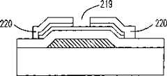
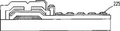
请参阅图2(a)至图2(h1),它们是本发明为改善现有技术而发展出来的薄膜晶体管制造方法的一较佳实施例步骤示意图,其中图2(a)表示出在一绝缘基板211上形成一第一导体层(可用铬、钼化钨、钽、铝或铜来完成)后以第一道光罩微影蚀刻制造来形成一闸极导体结构212,接着如图2(b)所示,由下而上依序形成一绝缘层213、一半导体层214(通常为非晶硅层(A-Si))、一高掺杂半导体层215(通常为N+非晶硅层(n+-A-Si)),然后如图2(c)所示,接着连续利用第二道光罩微影蚀刻制造来形成半导体结构216、一高掺杂半导体结构217。如图2(d)所示再沉积一第二导体层218,然后如图2(e)所示,以第三道光罩微影蚀刻制造来形成一导体结构220,并于所述高掺杂半导体结构217与所述导体结构形成一信道结构219以使所述导体结构形成有一源/漏极结构。图2(f)表示出于所述源/漏极结构上形成一保护层(通常为氮化硅层)221后,再以第四道光罩微影蚀刻制造形成一接触窗结构222。图2(g)表示进行一透明电极层(通常为氧化铟锡(ITO))的沉积后,再以第五道光罩微影蚀刻制造形成所需的一透明电极像素区域223。最后图2(h1)(h2)则分别表示于所述透明电极层的上方形成一第三导体层,并以第六道光罩微影蚀刻制造形成一锥状的导体结构224、225,随蚀刻剂浓度、时间、温度...控制的改变,可能会形成有圆椎状的导体结构224或椎柱状的导体结构225等不同的锥状的导体结构,但其较佳处在于所述锥状的导体结构224、225其具有与水平面呈3~20°的倾斜角度,可借以适当地改变光散射角度。Please refer to Fig. 2 (a) to Fig. 2 (h1), they are a schematic diagram of steps of a preferred embodiment of the thin film transistor manufacturing method developed in order to improve the prior art in the present invention, wherein Fig. 2 (a) shows that in a A first conductor layer (which can be completed by chromium, tungsten molybdenum, tantalum, aluminum or copper) is formed on the
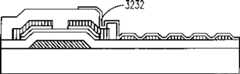
请参阅图3(a)至图3(g4),它们是本发明为改善现有技术而发展出来的薄膜晶体管制造方法的另一较佳实施例步骤示意图,其中图3(a)表示出在一绝缘基板311上形成一第一导体层(可用铬、钼化钨、钽、铝或铜来完成)后以第一道光罩微影蚀刻制造来形成一闸极导体结构312,接着如图3(b)所示,由下而上依序形成一绝缘层313、一半导体层314(通常为非晶硅层(A-Si))、一高掺杂半导体层315(通常为N+非晶硅层(n+-A-Si)),然后如图3(c)所示,接着连续利用第二道光罩微影蚀刻制造来形成半导体结构316、一高掺杂半导体结构317。如图3(d)所示再沉积一第二导体层3 18,然后如图3(e1)(e2)所示,以第三道光罩微影蚀刻制造来形成一导体结构320,并于所述高掺杂半导体结构318与所述导体结构形成一信道结构319以使所述导体结构形成有一源/漏极结构,接着以第四道光罩微影蚀刻制造形成一锥状的导体结构3211、3212,随蚀刻剂浓度、时间、温度...控制的改变,可能会形成有圆椎状的导体结构3211或椎柱状的导体结构3212等不同的锥状的导体结构,但其较佳处在于所述锥状的导体结构3211、3212其具有与水平面呈3~20°的倾斜角度,可借以适当地改变光散射角度。图3(f1)(f2)表示出于所述源/漏极结构上形成一保护层(通常为氮化硅层)322后,再以第五道光罩微影蚀刻制造形成一接触窗结构323。图3(g1)(g2)是表示出进行一透明电极层(通常为氧化铟锡(ITO))的沉积后,再以第六道光罩微影蚀刻制造形成所需的一透明电极像素区域3231、3232。Please refer to Fig. 3 (a) to Fig. 3 (g4), they are the step schematic diagrams of another preferred embodiment of the thin film transistor manufacturing method developed in order to improve the prior art, wherein Fig. 3 (a) shows the A first conductor layer (which can be completed by chromium, tungsten molybdenum, tantalum, aluminum or copper) is formed on an insulating substrate 311, and then a gate conductor structure 312 is formed by the first photomask lithography etching, and then as shown in the figure 3(b), an insulating layer 313, a semiconductor layer 314 (usually amorphous silicon layer (A-Si)), and a highly doped semiconductor layer 315 (usually N+ non- crystalline silicon layer (n+ -A-Si)), and then, as shown in FIG. As shown in Figure 3(d), a second conductor layer 318 is deposited, and then as shown in Figure 3(e1)(e2), a
本发明的椎状导体结构的形成,更可借由下列步骤来实现:The formation of the vertebral conductor structure of the present invention can be realized by the following steps:
首先沉积双层的薄膜金属,例如钼-铬(Mo-Cr)薄膜合金200nm厚度在下层及铝薄膜合金50nm厚度在上层,经由光罩进行曝光及显影制造形成留存区域,再以适当的蚀刻配方,例如磷酸(H3PO4)、硝酸(HNO3)及醋酸(CH3COOH)中任其二种或三种的混合酸,最后利用控制此双层薄膜的过蚀刻(over-etching)时间,并搭配适当的光罩线宽(3μm~10μm)即可有效控制倾斜角度(≤20°),进而可形成一圆椎状或椎柱状的结构。First deposit a double-layer thin film metal, such as molybdenum-chromium (Mo-Cr) thin film alloy 200nm thickness on the lower layer and aluminum thin film alloy 50nm thickness on the upper layer, and then expose and develop through a photomask to form a reserved area, and then use an appropriate etching formula , such as phosphoric acid (H3 PO4 ), nitric acid (HNO3 ) and acetic acid (CH3 COOH), any two or three mixed acids, and finally control the over-etching (over-etching) time of this double-layer film , and with an appropriate mask line width (3 μm ~ 10 μm), the tilt angle (≤20°) can be effectively controlled, and then a conical or columnar structure can be formed.
本发明的又一较佳处在于本发明提供一具有反射式或半穿透式式薄膜晶体管液晶显示器,因此,所述透明电极层(通常为氧化铟锡(ITO))亦可为一第三导电层,图3(g3)(g4)是表示出进行所述第三导电层的沉积后,再以第六道光罩微影蚀刻制造形成所需的一电极像素区域3233、3234。Another preferred feature of the present invention is that the present invention provides a reflective or semi-transmissive thin film transistor liquid crystal display, therefore, the transparent electrode layer (usually indium tin oxide (ITO)) can also be a third Conductive layer, FIG. 3(g3)(g4) shows that after the deposition of the third conductive layer, the required
Claims (18)
Translated fromChinesePriority Applications (1)
| Application Number | Priority Date | Filing Date | Title |
|---|---|---|---|
| CNB011406941ACN1185685C (en) | 2001-09-20 | 2001-09-20 | Thin film transistor liquid crystal display and manufacturing method thereof |
Applications Claiming Priority (1)
| Application Number | Priority Date | Filing Date | Title |
|---|---|---|---|
| CNB011406941ACN1185685C (en) | 2001-09-20 | 2001-09-20 | Thin film transistor liquid crystal display and manufacturing method thereof |
Publications (2)
| Publication Number | Publication Date |
|---|---|
| CN1405612A CN1405612A (en) | 2003-03-26 |
| CN1185685Ctrue CN1185685C (en) | 2005-01-19 |
Family
ID=4676000
Family Applications (1)
| Application Number | Title | Priority Date | Filing Date |
|---|---|---|---|
| CNB011406941AExpired - LifetimeCN1185685C (en) | 2001-09-20 | 2001-09-20 | Thin film transistor liquid crystal display and manufacturing method thereof |
Country Status (1)
| Country | Link |
|---|---|
| CN (1) | CN1185685C (en) |
Families Citing this family (1)
| Publication number | Priority date | Publication date | Assignee | Title |
|---|---|---|---|---|
| JP2005121908A (en)* | 2003-10-16 | 2005-05-12 | Advanced Display Inc | Reflection-type liquid crystal display, semi-transparent liquid crystal display, and method for manufacturing the same |
- 2001
- 2001-09-20CNCNB011406941Apatent/CN1185685C/ennot_activeExpired - Lifetime
Also Published As
| Publication number | Publication date |
|---|---|
| CN1405612A (en) | 2003-03-26 |
Similar Documents
| Publication | Publication Date | Title |
|---|---|---|
| KR100446562B1 (en) | Translucent Liquid Crystal Display Device | |
| KR100531410B1 (en) | Arrau Substrate for Trans-Reflection type Liquid Crystal Display Device and the Method of Manufacturing the same | |
| RU2503051C2 (en) | Liquid crystal display panel, method of making said panel and liquid crystal display device | |
| JP4499481B2 (en) | Liquid crystal display device and manufacturing method thereof | |
| JP2002357844A (en) | Liquid crystal display device and manufacturing method therefor | |
| JP5010586B2 (en) | Liquid crystal display device and method of manufacturing liquid crystal display device | |
| CN108594550B (en) | Array substrate and manufacturing method thereof | |
| US6292241B1 (en) | Reflective liquid crystal display apparatus with low manufacturing cost | |
| US8890153B2 (en) | Active matrix substrate and display device | |
| TW517393B (en) | TFT LCD structure with protrusion structure and its manufacturing method | |
| CN101063779A (en) | Liquid crystal display device and method of manufacturing the same | |
| CN108257976B (en) | TFT substrate and manufacturing method thereof | |
| CN101432656A (en) | Liquid crystal display device and method of manufacturing liquid crystal display device | |
| CN100481496C (en) | LCD and thin film transistor array panel thereof | |
| CN105702687A (en) | TFT (Thin Film Transistor) substrate and manufacturing method thereof | |
| CN101059612B (en) | Method for manufacturing semi-transmissive and semi-reflective liquid crystal panel and active element array substrate | |
| CN106298646A (en) | The manufacture method of TFT substrate | |
| CN101666949B (en) | IPS type TFT-LCD array substrate and manufacturing method thereof | |
| US20040104434A1 (en) | Thin film transistor liquid crystal display and method for manufacturing the same | |
| JPWO2007129480A1 (en) | Transflective liquid crystal display device and manufacturing method thereof | |
| CN1185685C (en) | Thin film transistor liquid crystal display and manufacturing method thereof | |
| CN1854838A (en) | Semi-transmissive and semi-reflective liquid crystal display panel and manufacturing method thereof | |
| US20060023134A1 (en) | Array substrate, manufacturing method thereof and display device having the same | |
| CN1265239C (en) | Wide Viewing Angle LCD Flat Panel Display | |
| CN101330087B (en) | Array substrate, manufacturing method thereof, and display device having the array substrate |
Legal Events
| Date | Code | Title | Description |
|---|---|---|---|
| C10 | Entry into substantive examination | ||
| SE01 | Entry into force of request for substantive examination | ||
| C06 | Publication | ||
| PB01 | Publication | ||
| C10 | Entry into substantive examination | ||
| SE01 | Entry into force of request for substantive examination | ||
| C10 | Entry into substantive examination | ||
| SE01 | Entry into force of request for substantive examination | ||
| C14 | Grant of patent or utility model | ||
| GR01 | Patent grant | ||
| CX01 | Expiry of patent term | Granted publication date:20050119 | |
| CX01 | Expiry of patent term |