CN1172270A - Liquid crystal display device and manufacturing method thereof - Google Patents
Liquid crystal display device and manufacturing method thereofDownload PDFInfo
- Publication number
- CN1172270A CN1172270ACN97111285ACN97111285ACN1172270ACN 1172270 ACN1172270 ACN 1172270ACN 97111285 ACN97111285 ACN 97111285ACN 97111285 ACN97111285 ACN 97111285ACN 1172270 ACN1172270 ACN 1172270A
- Authority
- CN
- China
- Prior art keywords
- substrate
- liquid crystal
- pixel
- active matrix
- display device
- Prior art date
- Legal status (The legal status is an assumption and is not a legal conclusion. Google has not performed a legal analysis and makes no representation as to the accuracy of the status listed.)
- Granted
Links
Images


Classifications
- G—PHYSICS
- G02—OPTICS
- G02F—OPTICAL DEVICES OR ARRANGEMENTS FOR THE CONTROL OF LIGHT BY MODIFICATION OF THE OPTICAL PROPERTIES OF THE MEDIA OF THE ELEMENTS INVOLVED THEREIN; NON-LINEAR OPTICS; FREQUENCY-CHANGING OF LIGHT; OPTICAL LOGIC ELEMENTS; OPTICAL ANALOGUE/DIGITAL CONVERTERS
- G02F1/00—Devices or arrangements for the control of the intensity, colour, phase, polarisation or direction of light arriving from an independent light source, e.g. switching, gating or modulating; Non-linear optics
- G02F1/01—Devices or arrangements for the control of the intensity, colour, phase, polarisation or direction of light arriving from an independent light source, e.g. switching, gating or modulating; Non-linear optics for the control of the intensity, phase, polarisation or colour
- G02F1/13—Devices or arrangements for the control of the intensity, colour, phase, polarisation or direction of light arriving from an independent light source, e.g. switching, gating or modulating; Non-linear optics for the control of the intensity, phase, polarisation or colour based on liquid crystals, e.g. single liquid crystal display cells
- G02F1/133—Constructional arrangements; Operation of liquid crystal cells; Circuit arrangements
- G02F1/1333—Constructional arrangements; Manufacturing methods
- G02F1/1339—Gaskets; Spacers; Sealing of cells
- G02F1/13392—Gaskets; Spacers; Sealing of cells spacers dispersed on the cell substrate, e.g. spherical particles, microfibres
- G—PHYSICS
- G02—OPTICS
- G02F—OPTICAL DEVICES OR ARRANGEMENTS FOR THE CONTROL OF LIGHT BY MODIFICATION OF THE OPTICAL PROPERTIES OF THE MEDIA OF THE ELEMENTS INVOLVED THEREIN; NON-LINEAR OPTICS; FREQUENCY-CHANGING OF LIGHT; OPTICAL LOGIC ELEMENTS; OPTICAL ANALOGUE/DIGITAL CONVERTERS
- G02F1/00—Devices or arrangements for the control of the intensity, colour, phase, polarisation or direction of light arriving from an independent light source, e.g. switching, gating or modulating; Non-linear optics
- G02F1/01—Devices or arrangements for the control of the intensity, colour, phase, polarisation or direction of light arriving from an independent light source, e.g. switching, gating or modulating; Non-linear optics for the control of the intensity, phase, polarisation or colour
- G02F1/13—Devices or arrangements for the control of the intensity, colour, phase, polarisation or direction of light arriving from an independent light source, e.g. switching, gating or modulating; Non-linear optics for the control of the intensity, phase, polarisation or colour based on liquid crystals, e.g. single liquid crystal display cells
- G02F1/133—Constructional arrangements; Operation of liquid crystal cells; Circuit arrangements
- G02F1/136—Liquid crystal cells structurally associated with a semi-conducting layer or substrate, e.g. cells forming part of an integrated circuit
- G02F1/1362—Active matrix addressed cells
- G02F1/136209—Light shielding layers, e.g. black matrix, incorporated in the active matrix substrate, e.g. structurally associated with the switching element
- G—PHYSICS
- G02—OPTICS
- G02F—OPTICAL DEVICES OR ARRANGEMENTS FOR THE CONTROL OF LIGHT BY MODIFICATION OF THE OPTICAL PROPERTIES OF THE MEDIA OF THE ELEMENTS INVOLVED THEREIN; NON-LINEAR OPTICS; FREQUENCY-CHANGING OF LIGHT; OPTICAL LOGIC ELEMENTS; OPTICAL ANALOGUE/DIGITAL CONVERTERS
- G02F1/00—Devices or arrangements for the control of the intensity, colour, phase, polarisation or direction of light arriving from an independent light source, e.g. switching, gating or modulating; Non-linear optics
- G02F1/01—Devices or arrangements for the control of the intensity, colour, phase, polarisation or direction of light arriving from an independent light source, e.g. switching, gating or modulating; Non-linear optics for the control of the intensity, phase, polarisation or colour
- G02F1/13—Devices or arrangements for the control of the intensity, colour, phase, polarisation or direction of light arriving from an independent light source, e.g. switching, gating or modulating; Non-linear optics for the control of the intensity, phase, polarisation or colour based on liquid crystals, e.g. single liquid crystal display cells
- G02F1/133—Constructional arrangements; Operation of liquid crystal cells; Circuit arrangements
- G02F1/1333—Constructional arrangements; Manufacturing methods
- G02F1/133388—Constructional arrangements; Manufacturing methods with constructional differences between the display region and the peripheral region
- G—PHYSICS
- G02—OPTICS
- G02F—OPTICAL DEVICES OR ARRANGEMENTS FOR THE CONTROL OF LIGHT BY MODIFICATION OF THE OPTICAL PROPERTIES OF THE MEDIA OF THE ELEMENTS INVOLVED THEREIN; NON-LINEAR OPTICS; FREQUENCY-CHANGING OF LIGHT; OPTICAL LOGIC ELEMENTS; OPTICAL ANALOGUE/DIGITAL CONVERTERS
- G02F1/00—Devices or arrangements for the control of the intensity, colour, phase, polarisation or direction of light arriving from an independent light source, e.g. switching, gating or modulating; Non-linear optics
- G02F1/01—Devices or arrangements for the control of the intensity, colour, phase, polarisation or direction of light arriving from an independent light source, e.g. switching, gating or modulating; Non-linear optics for the control of the intensity, phase, polarisation or colour
- G02F1/13—Devices or arrangements for the control of the intensity, colour, phase, polarisation or direction of light arriving from an independent light source, e.g. switching, gating or modulating; Non-linear optics for the control of the intensity, phase, polarisation or colour based on liquid crystals, e.g. single liquid crystal display cells
- G02F1/133—Constructional arrangements; Operation of liquid crystal cells; Circuit arrangements
- G02F1/1333—Constructional arrangements; Manufacturing methods
- G02F1/1341—Filling or closing of cells
- G—PHYSICS
- G02—OPTICS
- G02F—OPTICAL DEVICES OR ARRANGEMENTS FOR THE CONTROL OF LIGHT BY MODIFICATION OF THE OPTICAL PROPERTIES OF THE MEDIA OF THE ELEMENTS INVOLVED THEREIN; NON-LINEAR OPTICS; FREQUENCY-CHANGING OF LIGHT; OPTICAL LOGIC ELEMENTS; OPTICAL ANALOGUE/DIGITAL CONVERTERS
- G02F1/00—Devices or arrangements for the control of the intensity, colour, phase, polarisation or direction of light arriving from an independent light source, e.g. switching, gating or modulating; Non-linear optics
- G02F1/01—Devices or arrangements for the control of the intensity, colour, phase, polarisation or direction of light arriving from an independent light source, e.g. switching, gating or modulating; Non-linear optics for the control of the intensity, phase, polarisation or colour
- G02F1/13—Devices or arrangements for the control of the intensity, colour, phase, polarisation or direction of light arriving from an independent light source, e.g. switching, gating or modulating; Non-linear optics for the control of the intensity, phase, polarisation or colour based on liquid crystals, e.g. single liquid crystal display cells
- G02F1/133—Constructional arrangements; Operation of liquid crystal cells; Circuit arrangements
- G02F1/136—Liquid crystal cells structurally associated with a semi-conducting layer or substrate, e.g. cells forming part of an integrated circuit
- G02F1/1362—Active matrix addressed cells
- G02F1/136227—Through-hole connection of the pixel electrode to the active element through an insulation layer
Landscapes
- Physics & Mathematics (AREA)
- Nonlinear Science (AREA)
- Mathematical Physics (AREA)
- Chemical & Material Sciences (AREA)
- Crystallography & Structural Chemistry (AREA)
- General Physics & Mathematics (AREA)
- Optics & Photonics (AREA)
- Engineering & Computer Science (AREA)
- Microelectronics & Electronic Packaging (AREA)
- Liquid Crystal (AREA)
- Thin Film Transistor (AREA)
- Devices For Indicating Variable Information By Combining Individual Elements (AREA)
Abstract
Description
Translated fromChinese本发明涉及一种在同一衬底上设置有矩阵形式的像素区域的液晶显示装置,特别是一种采用半导体薄膜的带半导体装置的有源矩阵型液晶显示装置。上述半导体薄膜可典型地选用硅薄膜。The present invention relates to a liquid crystal display device provided with pixel regions in a matrix form on the same substrate, in particular to an active matrix liquid crystal display device with a semiconductor device using a semiconductor thin film. The above-mentioned semiconductor thin film can typically be a silicon thin film.
当今时代,利用半导体薄膜,例如薄膜晶体管(TFT),在廉价玻璃衬底上制作半导体装置的技术正得到迅速发展,其原因在于对有源基片型液晶显示装置需求的增加。In the present era, the technology of fabricating semiconductor devices on inexpensive glass substrates using semiconductor thin films such as thin film transistors (TFTs) is rapidly developing due to the increasing demand for active substrate type liquid crystal display devices.
对于一有源矩阵型液晶显示装置,在一基片上设置有几十到几百万个像素区域,对每一像素区域都设置有薄膜晶体管,向相应像素电极注入和从其输出的电荷由这些薄膜晶体管的开关功能进行控制。For an active matrix liquid crystal display device, tens to several million pixel regions are arranged on a substrate, and a thin film transistor is arranged for each pixel region, and charges injected into and output from corresponding pixel electrodes are obtained by these The switching function of the thin film transistor is controlled.
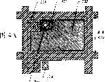
这里结合图1(A)和1(B)解释设置有薄膜晶体管的有源基片型液晶显示装置的基本结构。首先,图1(A)为图1(B)所示的液晶显示装置沿与衬底垂直方向的部分剖视图,此部分对应于图1(B)中由剖面线A-A’所切割的部分。Here, the basic structure of an active substrate type liquid crystal display device provided with a thin film transistor is explained with reference to FIGS. 1(A) and 1(B). First, FIG. 1(A) is a partial cross-sectional view of the liquid crystal display device shown in FIG. 1(B) along a direction perpendicular to the substrate, and this part corresponds to the part cut by the section line AA' in FIG. 1(B) .
数字101表示透明衬底,其中形成一层绝缘薄膜(未画出),数字102表示薄膜晶体管(TFT)的有源层,数字103表示门电极,数字104表示数据线,数字105表示漏电极,数字106表示的为层间绝缘膜,数字107所示为一黑色基片,数字108所示为像素电极,包含一透明导电膜,数字109表示平行层。
带有上述结构薄膜晶体管的整个衬底在后面将称为有源矩阵衬底。虽然按照图1(A)只考虑了一个像素区域,但实际上这种有源矩阵衬底由数十个至数百万个像素区域构成,并有驱动电路来驱动这些像素区域。The entire substrate with the thin film transistors of the above structure will be referred to as an active matrix substrate hereinafter. Although only one pixel area is considered according to FIG. 1(A), in reality this active matrix substrate is composed of tens to millions of pixel areas, and there are driving circuits to drive these pixel areas.
同时,数字110所示为透明衬底,数字111所示为由一透明导电膜构成的相对电极。数字112所示为定向层。有上述构造并且与前述有源矩阵衬底相对的这种整个衬底称为相对衬底。Meanwhile,
在经过后面步骤的研磨处理以使液晶材料的定向层调整后,有源矩阵衬底和相对衬底由一密封部件相对地合在一起,图中没有显示。After the grinding treatment in the later step to adjust the alignment layer of the liquid crystal material, the active matrix substrate and the opposite substrate are relatively joined together by a sealing member, not shown in the figure.
在此例中,在该两种衬底之间插有均匀密度的隔离物,未图示,从而可获得一均匀的衬底间隔(称为单元间距Cell Gap)。严格说来,在图1(A)所示结构的情况下,有源基片衬底上的定向层109与相对衬底上的定向层112之间的距离即为所述单元间距。In this example, spacers of uniform density are interposed between the two substrates, not shown, so that a uniform substrate spacing (called Cell Gap) can be obtained. Strictly speaking, in the case of the structure shown in FIG. 1(A), the distance between the
密封部件不仅作为将上述两衬底合在一起的粘接剂,还可用以将此两衬底间的液晶材料密封在一像显示区域,以构成大量像素区域。The sealing member is not only used as an adhesive for bonding the above two substrates together, but also can be used to seal the liquid crystal material between the two substrates in an image display area to form a large number of pixel areas.
因而,液晶材料113密封在像显示区(即大量像素区域中的每一个),如图1(A)所示。通过这种方法,可制成具有图1(A)所示结构的有源矩阵型液晶显示装置。Thus, the
按照图1(A)所示的像素区域,由薄膜晶体管控制的像信号就存储于由像素电极108和相对电极111构成的电容中,以液晶材料113作为其绝缘层。According to the pixel area shown in FIG. 1(A), the image signal controlled by the thin film transistor is stored in the capacitor formed by the
此时,在模拟灰度系统的情况下,在像素电极108与相对电极111之间就形成了与像信号电平相对应的电场。此外,像显示的不同灰度可通过利用液晶材料113随施加电压变化产生不同的光学响应的特征来实现。At this time, in the case of an analog grayscale system, an electric field corresponding to the image signal level is formed between the
向列型液晶材料(例如,TNC扭曲向列)型或者STN(超扭曲向列)型液晶材料)通常被用作液晶材料。按照图1(A)所示的液晶显示装置,其向列型液晶材料的特性在于,当施加电场时,此液晶的长轴方向与衬底大致平行(然而可有一预倾斜角),而当电场产生后,其长轴方向将与电场方向一致。A nematic liquid crystal material (eg, TNC twisted nematic) type or STN (super twisted nematic) type liquid crystal material) is generally used as the liquid crystal material. According to the liquid crystal display device shown in Fig. 1 (A), the characteristic of its nematic liquid crystal material is, when applying electric field, the long-axis direction of this liquid crystal is roughly parallel with substrate (but can have a pre-tilt angle), and when After the electric field is generated, the direction of its long axis will be consistent with the direction of the electric field.
于是,根据施加于此液晶材料上的电场的有无,其长轴方向呈相应的变化,因而通过根据其长轴方向的变化量来控制透光量,实现图像显示。Therefore, according to the presence or absence of an electric field applied to the liquid crystal material, the direction of its long axis changes accordingly, so by controlling the amount of light transmitted according to the amount of change in the direction of its long axis, image display is realized.
然而,只有在像素电极108与相对电极111之间形成的电场方向与衬底垂直时,液晶材料的此种行为才是可适用的。However, this behavior of the liquid crystal material is applicable only when the direction of the electric field formed between the
例如,在与衬底大致平行的水平电场产生的区域,由于产生准直缺陷,而干扰了液晶材料的准直度,从而不能产生所需图像。For example, in the region where the horizontal electric field is generated approximately parallel to the substrate, alignment defects are generated, which interfere with the alignment of the liquid crystal material, so that desired images cannot be produced.
通常,当单元间距与施加于像素电极108上的电压相适合时,垂直电场(与衬底正交的电场)占主要部分。但随着单元间距的增大,垂直电场的影响减弱,而水平电场的影响得以增强。Generally, when the cell pitch is suitable for the voltage applied to the
这里,图1(B)为像素区域的俯视图,由于水平方向电场的影响,使此液晶材料产生了准直缺陷。附带说一下,像显示区域以外的区域被黑色基片107遮盖。因而,黑色基片下显露的线路或类似物在图中由点划线表示出来。Here, FIG. 1(B) is a top view of the pixel region. Due to the influence of the electric field in the horizontal direction, alignment defects occur in the liquid crystal material. Incidentally, the area other than the image display area is covered by the
在图1(B)中,像显示区域(黑色基片107未遮盖的区域)形成的白线表示由液晶材料的准直缺陷引起的像显示干扰,即通常所指的畸变。这些区域处于发生异常的状态下,不同于液晶分子固有的排列状态。In FIG. 1(B), the white line formed in the image display area (the area not covered by the black substrate 107) indicates image display interference caused by alignment defects of the liquid crystal material, which is commonly referred to as distortion. These regions are in an abnormal state different from the inherent alignment state of the liquid crystal molecules.
作为发生畸变的一个原因,首先应指出的是由线路之间或薄膜晶体管之间的交叉干扰引起的水平电场的影响。As one of the causes of distortion, first of all, the influence of the horizontal electric field caused by crosstalk between lines or between thin film transistors should be pointed out.
例如,如图1(B)上部的像素区域所示,多数的畸变都由本发明人根据实验进行了观测。水平电场估计是由门电极103的前端与控制线114和数据线相交部分之间潜在差别引起的。For example, as shown in the upper pixel area of FIG. 1(B), most of the distortions were observed experimentally by the present inventors. The horizontal electric field estimate is caused by a potential difference between the front end of the
这种现象进一步表现为获得高质量的图像显示需减小像素区域的宽度(像素间距),即减小交线距离。当然,像素间距要受像素区域短边的限制。This phenomenon is further manifested in the need to reduce the width of the pixel area (pixel pitch) to obtain high-quality image display, that is, to reduce the intersection distance. Of course, the pixel pitch is limited by the short side of the pixel area.
另外,减小像素间距意味着相应增大单元间距,并可预计到水平电场的影响会进一步增强,除非单元间距根据像素间距作适当变化。In addition, reducing the pixel pitch means correspondingly increasing the cell pitch, and it can be expected that the influence of the horizontal electric field will be further enhanced unless the cell pitch is appropriately changed according to the pixel pitch.
与上述情况不同的是,还存在如图1(B)下部所示的畸变,根据观测,它是由液晶材料在为确保单元间距而设置的垫片115附近的排列的干扰而引起的。Different from the above case, there is also distortion as shown in the lower part of Fig. 1(B), which is caused by the disturbance of the arrangement of the liquid crystal material near the
而且,另一原因在于,线路或薄膜晶体管的外围形成的像素电极108的阶梯形差别。其问题在于,在压磨操作中未完成准直处理时,由于阶梯形差别的存在,或由于其侧面水平电场而导致在阶梯形差别的外围产生畸变。Moreover, another reason is that the step shape of the
几乎所有在阶梯形差别的外围产生的畸变都被黑色基片遮盖和隐藏了。然而,仅有使有源层102和像素电极108彼此接触的一个接触部分不会被黑色基片107遮盖,从而那里可观察到畸变。Almost all distortions that occur at the periphery of the step-shaped difference are covered and hidden by the black substrate. However, only a contact portion where the
在液晶显示装置的像素区域所形成的畸变产生了极不舒适的视觉感受,例如使显示图像的整体发生模糊,或类似情况。The distortion formed in the pixel area of the liquid crystal display device produces extremely uncomfortable visual experience, such as blurring the entire displayed image, or the like.
本说明书公开的发明目的在于,实现一种能提供高质量图像,不产生如上所述缺点的畸变的液晶显示装置。An object of the invention disclosed in this specification is to realize a liquid crystal display device capable of providing high-quality images without causing distortions, which are disadvantageous as described above.
如上所述,这种畸变现象表现在像素间距的参数,单元间距以及在薄膜晶体管或类似物的外围产生的阶梯形差别的高度上。As described above, this distortion phenomenon appears in the parameters of the pixel pitch, the cell pitch, and the height of the step-shaped difference produced at the periphery of the thin film transistor or the like.
因此,本申请人设想在像素间距与单元间距之间存在某种相关关系,并且根据像素间距,其单元间距存在一允许值。而且,他们认为在压磨操作中,会增加准直缺陷的阶梯形差别也存在一允许界限。Therefore, the present applicant assumes that there is a certain correlation between the pixel pitch and the cell pitch, and that there is an allowable value for the cell pitch according to the pixel pitch. Furthermore, they considered that there is an allowable margin for step-shaped differences that would increase alignment defects during the milling operation.
在本申请人根据实际生产液晶显示装置指导众多研究的基础上,逐渐获得如下认识。On the basis of numerous researches directed by the present applicant based on the actual production of liquid crystal display devices, the following knowledge was gradually obtained.
根据本发明的一个方面,它提供了一种液晶显示装置,包括一有源矩阵衬底,它包含有在同一衬底以矩阵形式设置的控制线和数据线,一个设置在像素区域周围有两个邻近控制线和两个邻近数据线的薄膜晶体管,和一个与此薄膜晶体管相连的像素电极;一相对衬底,包括其表面的相对电极,大量隔离物和注入在上述有源矩阵衬底和相对衬底之间的液晶材料,其中有源矩阵衬底与相对衬底之间的间隔为像素区域的像素间距的十分之一或更小。According to one aspect of the present invention, it provides a liquid crystal display device, including an active matrix substrate, which includes control lines and data lines arranged in a matrix on the same substrate, one arranged around the pixel area with two A thin film transistor adjacent to the control line and two adjacent data lines, and a pixel electrode connected to the thin film transistor; an opposite substrate, including an opposite electrode on its surface, a large number of spacers and implants in the above active matrix substrate and The liquid crystal material between the opposite substrates, wherein the space between the active matrix substrate and the opposite substrate is one-tenth or smaller than the pixel pitch of the pixel area.
例如,即使像素间距值变化,其单元间距的允许值也相应变化,从而总的尺寸保持不变。这就是说,当控制液晶显示装置的驱动电压时,对驱动液晶层不产生相反影响。For example, even if the pixel pitch value changes, the allowable value of its cell pitch changes accordingly, so that the overall size remains the same. That is, when controlling the driving voltage of the liquid crystal display device, there is no adverse effect on driving the liquid crystal layer.
因此,本发明的应用不依赖于像素间距的大小。然而,由于当前技术的限制,其像素间距或单元间距采用的数值存在一个限制。对比,将参照实施例1作出解释。Therefore, the application of the present invention does not depend on the size of the pixel pitch. However, due to the limitations of current technology, there is a limit to the value used for its pixel pitch or cell pitch. For comparison, explanation will be made with reference to Example 1.
有源矩阵衬底与相对衬底的间隔决定于插入其中的隔离物。因此,散布在有源矩阵衬底上的大量隔离物的直径(沿与衬底垂直方向的直径)必须为像素间距的十分之一或更小。The spacing between the active matrix substrate and the opposite substrate is determined by spacers inserted therein. Therefore, the diameter (the diameter in the direction perpendicular to the substrate) of a large number of spacers dispersed on the active matrix substrate must be one-tenth or less of the pixel pitch.
此外,由于有源矩阵衬底的结构致使薄膜晶体管或导线的外围存在阶梯形差别,因而单元间距的最大间距(位于像素区域平面部分的单元间距)必须满足上述间隔条件。In addition, due to the structure of the active matrix substrate, there is a step difference in the periphery of the thin film transistor or the wire, so the maximum pitch of the cell pitch (cell pitch in the plane part of the pixel area) must meet the above spacing conditions.
而且,本发明人发现,在像素间距与阶梯形差别高度之间还存一相关关系。根据本发明人的研究,如果这种阶梯形差别的高度为0.3μm或更小,则压磨操作的实现毫无问题,从而可制造出一种其水平电场的影响可忽略不计并且不会产生畸变的液晶显示装置。Moreover, the inventors have found that there is a correlation between the pixel pitch and the height of the step-shaped difference. According to the research of the present inventors, if the height of this step-shaped difference is 0.3 μm or less, then there is no problem in the realization of the milling operation, so that it is possible to manufacture a product whose influence of the horizontal electric field is negligible and does not produce Distorted liquid crystal display device.
根据本发明的另一方面,它提供了一种制造液晶显示装置的方法,它包括如下步骤:制造一有源矩阵衬底,它包括设在同一衬底上矩阵形式的的控制线和数据线,一个设在像素区域的薄膜晶体管,外围有两个邻近的控制线和两个邻近的数据线以及一个像素电极与其相连;制造一相对衬底,它包含一在其表面的相对电极;在此有源矩阵衬底和相对衬底之间设置大量垫片并注入液晶材料,其中有源矩阵衬底和相对衬底之间的所述间隔应为像素区的像素间隔的十分之一。According to another aspect of the present invention, it provides a method of manufacturing a liquid crystal display device, which includes the steps of: manufacturing an active matrix substrate, which includes control lines and data lines in a matrix form on the same substrate , a thin film transistor arranged in a pixel area, with two adjacent control lines and two adjacent data lines and a pixel electrode connected to it on the periphery; an opposite substrate is manufactured, which includes an opposite electrode on its surface; here A large number of spacers are arranged between the active matrix substrate and the opposite substrate and liquid crystal material is injected, wherein the distance between the active matrix substrate and the opposite substrate should be one tenth of the pixel interval of the pixel area.
根据本发明的又一方面,它提供了一种制造液晶显示装置的方法,包括如下步骤:制造一有源矩阵衬底,它包括设在同一衬底上矩阵形式的控制线和数据线,一个设在像素区域的外围围绕有邻近的两个控制线和邻近的两个数据线的薄膜晶体管,一个与此薄膜晶体管相连的漏电极,一覆盖此漏电极的层间绝缘膜,和通过此层间绝缘膜上的一个接触孔与每个漏电极相连的像素电极;制造一个其表面含有一相对电极的相对衬底;在上述有源矩阵衬底和相对衬底之间装备液晶材料,其中漏电极的膜厚为0.3μm或更小。According to yet another aspect of the present invention, it provides a method for manufacturing a liquid crystal display device, comprising the steps of: manufacturing an active matrix substrate, which includes control lines and data lines in a matrix form on the same substrate, a Thin film transistors with two adjacent control lines and two adjacent data lines surrounding the periphery of the pixel area, a drain electrode connected to the thin film transistor, an interlayer insulating film covering the drain electrode, and through this layer A contact hole on the interlayer insulating film is connected to a pixel electrode of each drain electrode; an opposite substrate having an opposite electrode on its surface is manufactured; a liquid crystal material is provided between the above-mentioned active matrix substrate and the opposite substrate, wherein the leakage current The film thickness of the electrode is 0.3 μm or less.
图1(A)和1(B)显示了液晶显示装置的结构;1(A) and 1(B) show the structure of a liquid crystal display device;
图2(A),2(B),2(C),2(D)和2(E)说明了有源矩阵衬底的制作步骤;Fig. 2 (A), 2 (B), 2 (C), 2 (D) and 2 (E) have illustrated the fabrication steps of active matrix substrate;
图3(A),3(B),3(C)和3(D)说明了单元的集成步骤;Figure 3(A), 3(B), 3(C) and 3(D) illustrate the integration steps of the unit;
图4(A)和4(B)显示了液晶显示装置的构造。4(A) and 4(B) show the configuration of a liquid crystal display device.
下面结合具体实施例对具有上述结构的本发明的细节进行解释。实施例1The details of the present invention having the above structure will be explained below in conjunction with specific embodiments. Example 1
实施例1将详细解释在本发明基础上的液晶显示装置的制造步骤。参照图2(A),2(B),2(C),2(D)和2(E),将解释TFT(薄膜晶体管)电路和设在一有源基片衬底上的像素TFT的制造步骤,并将参照图3(A),3(B),3(C)和3(D)解释所述液晶显示装置的制造步骤(单元的集成步骤)。Embodiment 1 will explain in detail the manufacturing steps of a liquid crystal display device based on the present invention. 2 (A), 2 (B), 2 (C), 2 (D) and 2 (E), will explain the TFT (Thin Film Transistor) circuit and the pixel TFT provided on an active substrate substrate. Manufacturing steps, and manufacturing steps (unit integration steps) of the liquid crystal display device will be explained with reference to FIGS. 3(A), 3(B), 3(C) and 3(D).
附带地,将注意到像素间距与单元间距(Cell Gap)之间的主要相关关系对实施例1进行描述。因此,在实施例1中将不考虑处于无影响水平的0.3μm或更小的阶梯形差异,并且对此不作解释。Incidentally, Embodiment 1 will be described with attention to the main correlation between the pixel pitch and the cell pitch (Cell Gap). Therefore, a step-shaped difference of 0.3 μm or less at an insignificant level will not be considered in Example 1 and will not be explained.
首先,应准备具有绝缘性能的一块衬底,例如以康宁(Corning)7059或康宁1737或类似物为代表的玻璃衬底201,在玻璃衬底201上形成一厚度为2000A的硅氧化物膜作为垫层202。First, a substrate with insulating properties should be prepared, such as a
然后,形成一厚度为500A的非晶态硅薄膜,图中设有显示。在制作此膜的过程中,可采用等离子体CVD(化学气相沉积)工艺或低压热力CVD工艺。Then, an amorphous silicon film with a thickness of 500A is formed, as shown in the figure. In the process of making this film, a plasma CVD (Chemical Vapor Deposition) process or a low-pressure thermal CVD process can be used.
在非晶硅膜层(未图示)制成后,通过适当的结晶工艺使其实现结晶,在其上制成一晶态硅膜层(未图示),例如通常利用受激激光或类似物在约600℃时进行退火的热处理方法。After the amorphous silicon film layer (not shown) is made, it is crystallized by an appropriate crystallization process, and a crystalline silicon film layer (not shown) is formed on it, for example, usually using a stimulated laser or the like A heat treatment method in which the object is annealed at about 600°C.
而且,这里可采用一种方法来形成非晶态硅薄膜,包括至少一种在结晶步骤中能有助于非晶硅薄膜结晶的金属元素。此方法的细节在日本待审查专利说明书No.6-232059和No.7-321339中有所描述。根据此方法,通过在短时间内进行相当低温的热处理可获得具有优越结晶度的硅薄膜。Also, there may be employed a method for forming an amorphous silicon thin film including at least one metal element that can assist crystallization of the amorphous silicon thin film in the crystallization step. Details of this method are described in Japanese Unexamined Patent Specifications No. 6-232059 and No. 7-321339. According to this method, a silicon thin film having excellent crystallinity can be obtained by performing heat treatment at a relatively low temperature in a short period of time.
通过上述方法进行热处理获得的晶态硅薄膜,可采用激光或具有相当能量的强光对其进行有效的退火。因而,此硅薄膜的结晶度可得到显著改善。The crystalline silicon thin film obtained by heat treatment in the above method can be effectively annealed by laser or strong light with considerable energy. Thus, the crystallinity of the silicon thin film can be significantly improved.
然后,将所得的晶态硅薄膜制成下列结构,它具有一个构成电路TFT有源层的岛状半导体层203和一个构成像素TFT有源层的岛状半导体层204(见图2(A))。Then, the obtained crystalline silicon film is made into the following structure, which has an island-shaped
在此有源层制成后,在其上通过等离子体CVD工艺形成一厚度为1200A的硅氧化物薄膜加以覆盖。此硅氧化物薄膜205其以后的功能在于作为门绝缘膜。另外,也可采用硅氮氧化物(例如,由SiOxNy表示的化合物)薄膜或硅氮化物薄膜。After the active layer is fabricated, a silicon oxide film with a thickness of 1200A is formed on it by plasma CVD process to cover it. This
然后,通过溅射形成一厚度为2500的掺有按重量计0.2%钪的铝膜206,加入钪能有效地抑制在铝膜表面的小丘或晶须的出现。此铝膜206其后面的功能在于作为一门电极。Then, an
附带地,其他金属材料薄膜,如Mo,Ti,Ta,Cr,或类似金属也可用以替代铝膜,并可采用例如多晶硅或硅化物类材料的具有导电性的薄膜。Incidentally, other metal material films, such as Mo, Ti, Ta, Cr, or similar metals can also be used instead of the aluminum film, and conductive films such as polysilicon or silicide-like materials can be used.
然后,在电解液中,以铝膜206作为阳极进行阳极氧化。此电解液可采用下述溶液,含3%酒石酸的乙二醇溶液,由氨水中和并使其酸度调整至pH=6.92。Then, in an electrolytic solution, anodic oxidation is performed using the
而且,以铂作为阴极,在化学电流5mA和电压10V的条件下实现此反应。Furthermore, the reaction was carried out under the conditions of chemical current 5mA and voltage 10V with platinum as the cathode.
以此方法制作的一层紧密的阳极氧化物薄膜(未给出图示),在后面步骤中对于提高光刻胶的附着力是有效的。此膜的厚度可通过控制电压的施加时间加以控制(图2(A))。A dense anodic oxide film (not shown) produced in this way is effective in improving the adhesion of photoresist in the subsequent steps. The thickness of this film can be controlled by controlling the application time of the voltage (FIG. 2(A)).
在图2(A)状态由此方式提供后,此铝膜206就被制成门电极和数据线的试样(未给出图示),它将在后面步骤中用到。另外,可采用另一种阳极氧化来形成疏松的阳极氧化物铝膜207和208,其电解液为含3%草酸的水溶液,并且以铂作为阴极在化学电流为2到3mA,电压为8V的条件下实现此反应(图2(B))。After the state of FIG. 2(A) is thus provided, the
第二种阳极氧化是在与衬底平行的方向进行的,此疏松阳极氧化物薄膜207和208的长度可通过控制电压施加时间进行控制。The second anodization is performed in a direction parallel to the substrate, and the length of the loose
另外,光刻胶可由一种专门使用的清除剂除去,实现第三种阳极氧化。在此情况下,其电解液采用含3%酒石酸的乙二醇溶液,由氨水中和并调整其酸度为pH=6.92。反应条件为以铂作为阴极,化学电流为5到6mA,电压为100V。In addition, the photoresist can be removed by a specially used scavenger to achieve a third type of anodization. In this case, the electrolyte is ethylene glycol solution containing 3% tartaric acid, neutralized by ammonia water and adjusted to pH=6.92. The reaction conditions are that platinum is used as the cathode, the chemical current is 5 to 6mA, and the voltage is 100V.
由此制成的阳极氧化物薄膜209和210很紧密并且牢固。因而,它们能有效保护门电极211和212免遭后续步骤如掺杂步骤或类似步骤的损坏。The thus formed
这种牢固的阳极氧化物薄膜209和210难于刻蚀,因而在制作接触孔时,其刻蚀时间应该延长。因此,其厚度最好为1000或更小。Such strong
然后,在图2(B)所示状态下,通过离子掺杂工艺将杂质注入有源层203和204。例如,在制作N通道型TFT时,可采用磷作为杂质,而在制作P通道型TFT时,可采用硼作为杂质。Then, in the state shown in FIG. 2(B), impurities are implanted into the
虽然实施例1仅描述了制作N通道型TFT的例子,但利用公知技术可在相同衬底上制作N通道型TFT和P通道型TFT。Although Embodiment 1 only describes an example of fabricating N-channel TFTs, N-channel TFTs and P-channel TFTs can be fabricated on the same substrate using known techniques.
通过离子注入可自调式地形成电路TFT的源/漏区域213和214以及像素TFT的源/漏区域215和216。The source/
清除掉疏松的阳极氧化物薄膜207和208并重新进行离子注入,此时的剂量应低于前面离子注入的剂量。The loose
低浓度的杂质区217和218以及电路TFT的通道形成区域221,和低浓度的杂质区219和220以及像素TFT的通道形成区222,通过第二种离子注入方式可自动调节形成。The low-
在如图2(C)所示状态下,相继实施激光照射和热处理。根据实施例1,其采用激光的能量密度为160到170mJ/cm2,热处理为300到450℃持续1小时。In the state shown in FIG. 2(C), laser irradiation and heat treatment are sequentially performed. According to the embodiment 1, the energy density of the laser is 160 to 170 mJ/cm2 , and the heat treatment is 300 to 450° C. for 1 hour.
通过此步骤,由离子搀入过程损坏的有源层203和204的结晶度得以提高,并使离子注入的杂质离子得以激活。Through this step, the crystallinity of the
然后,通过等离子体CVD工艺制成一厚度为3000的硅氮化物薄膜(可以是硅氧化物薄膜)作为第一层间绝缘膜223。此层间绝缘膜223可以具有多层结构。Then, a silicon nitride film (which may be a silicon oxide film) with a thickness of 3000 Å is formed as the first
在制成第一层间绝缘膜后,在电极及导线将要形成的区域制作接触孔。电路TFT的源线(可称作数据线)224,控制线225和漏线226以及像素TFT的源线227和漏电极228由铝作为主要成分和钛构成的叠层制得。After forming the first interlayer insulating film, contact holes are formed in the regions where electrodes and wires are to be formed. Source lines (may be referred to as data lines) 224,
在此情况下,像素TFT的门电极212与控制线合在一起(没有图示),延伸至像素区域的外部,因而不必制作接触孔。而且,漏极228在后将用作引线以连接像素电极和有源层。In this case, the
然后,通过等离子体CVD工艺制作一厚度为0.5到5μm的第二层间绝缘膜229。此层间绝缘膜229可采用单层或多层,包括硅氧化物薄膜,硅氮化物薄膜,有机树脂或类似物。Then, a second
当采用有机树脂材料例如聚酰亚胺或类似物作为第二层间绝缘膜229时,可方便地提供较大的膜厚,因而此第二层间绝缘膜229可提供平展膜的功能。也即,在有源矩阵衬底上的阶梯形差异可尽可能地减小。When an organic resin material such as polyimide or the like is used as the second
在第二层间绝缘膜229制成后,制成黑色基体230。此黑色基体230可采用金属薄膜,例如铬薄膜,钛薄膜或类似物或弥散有黑色颜料的树脂材料。After the second
当黑色基体230在有源矩阵衬底上形成后,由于其覆盖区域可由一必需的最小占据面积覆盖,使其孔径比率没有变差,所以这种结构是有效的。When the black matrix 230 is formed on the active matrix substrate, this structure is effective because its footprint can be covered by a necessary minimum footprint without deteriorating its aperture ratio.
在第三层间绝缘膜231形成后通过对其第二层间绝缘膜在像素TFT漏极228之上的部分进行刻蚀制成一接触孔,并且形成一个与漏极228电连接的像素电极232。After the formation of the third
通过这种方式制成如图2(E)所示的具有电路TFT与像素TFT的有源矩阵衬底。实际上,在驱动电路区域设置有几十万个电路的TFT以构成CMOS(补偿式金属氧化物半导体)电路和类似物,并在像素区域设置有几十到几百万个像素TFT。In this way, an active matrix substrate having circuit TFTs and pixel TFTs as shown in FIG. 2(E) is fabricated. Actually, hundreds of thousands of circuit TFTs are provided in the driver circuit area to constitute CMOS (Compensated Metal Oxide Semiconductor) circuits and the like, and several tens to several million pixel TFTs are provided in the pixel area.
附带地,实施例1中制造的有源矩阵衬底其像素区域应设计成使像显示区域的像素间距为50μm,像素间距一般随液晶显示装置的应用而有所不同,例如,在个人笔记本电脑中,采用的液晶面板其像素间距为约110μm。另外,如果像素间距大于必要值,将会使显示的图像变粗。Incidentally, the pixel area of the active matrix substrate manufactured in Example 1 should be designed so that the pixel pitch of the image display area is 50 μm, and the pixel pitch generally varies with the application of the liquid crystal display device, for example, in a personal notebook computer Among them, the pixel pitch of the liquid crystal panel used is about 110 μm. Also, if the pixel pitch is larger than necessary, it will make the displayed image thicker.
下面参照图3(A),3(B),3(C)和3(D)解释液晶单元的集成过程。在集成液晶单元时,除以上述步骤制成有源矩阵衬底外,还应制备其相对的透明衬底,它包括一相对电极和一定向层。The integration process of the liquid crystal cell is explained below with reference to FIGS. 3(A), 3(B), 3(C) and 3(D). When integrating the liquid crystal unit, in addition to making the active matrix substrate through the above steps, the opposite transparent substrate should also be prepared, which includes an opposite electrode and an alignment layer.
附带说一下,如果需显示一彩色图像,则尽管未特别说明也需在相对衬底一边设置一彩色滤波器,它需具有平滑,厚度均匀,和优越的耐热及耐化学腐蚀等类似的要求。Incidentally, if a color image is to be displayed, a color filter must be provided on the opposite side of the substrate although not specifically stated, and it must have smoothness, uniform thickness, and superior heat resistance and chemical corrosion resistance, etc. .
当制成有源矩阵衬底与相对衬底后,对此两衬底分别相继实施压磨操作,以使其定向层产生所需序列。在衬底附近的液晶材料的排列由此步决定。(图3(A))After the active matrix substrate and the opposite substrate are manufactured, the two substrates are subjected to grinding operations successively, so that the alignment layer can be in the desired sequence. The alignment of the liquid crystal material near the substrate is determined by this step. (Figure 3(A))
在压磨操作完成后,通过网板印刷在相对衬底上分别形成一密封部件306,以包围驱动电路区域和像素区域。可将溶于“乙基溶解剂”(ethycellsolve)溶液中的环氧树脂族树脂和苯酚固化剂用于此密封件306。另外,在此密封件306的一个部分应形成一开口部(液晶注入部),以便在后注入液晶材料。After the embossing operation is completed, a sealing
密封件306作用不仅在于使衬底粘接,而且也防止注入的液晶材料从像显示区域附近泄露。The function of the sealing
然后,在相对衬底上散布隔离物307。由聚合物类,玻璃类或二氧化硅类材料制成的球状细粒可用作此隔离物307,它们由一喷射器散布在相对衬底上面。(图3(B))
此隔离物307的直径必须是像素间距的十分之一或更小。这就是说,衬底之间的单元间距为像素间距的十分之一或更小这一点是重要的。实施例1中的像素间距为50μm,考虑到小的余量,隔离物307的直径可定为4μm。The diameter of this
在单元间距极窄的情况下,玻璃衬底的表面起伏或隔离物直径的误差都会产生影响。因此,目前单元间距的最低限为约1μm。因此,本发明由于实用限制,其液晶显示装置的像素间距约为10μm。In the case of extremely narrow cell pitches, surface relief of the glass substrate or tolerances in spacer diameters can play a role. Thus, the cell pitch currently has a lower limit of about 1 [mu]m. Therefore, due to the practical limitation of the present invention, the pixel pitch of the liquid crystal display device is about 10 μm.
为防止对TFT的污染和静电破坏,印刷密封件和散布隔离物的步骤在相对衬底上进行。因为会伴有静电产生,散布隔离物的步骤特别应选择在相对衬底上进行。To prevent contamination and electrostatic damage to the TFTs, the steps of printing seals and spreading spacers are performed on the opposite substrate. Because it will be accompanied by static electricity, the step of spreading spacers should be particularly selected to be carried out on the opposite substrate.
然后,将有源矩阵衬底和相对衬底粘合在一起。在粘合操作中,隔离物307应置于两衬底之间,其单元间距由隔离物307的直径决定。(图3(C))Then, the active matrix substrate and the opposite substrate are bonded together. During the bonding operation, a
如前所述,隔离物307的直径为4μm,因而衬底之间的单元间距也为4μm。均匀散布隔离物307和衬底的精确粘贴技术在本发明中由于其对提供精确单元间距的重要性而成为必需。As previously mentioned, the diameter of the
在完成对有源矩阵衬底和相对衬底的粘贴后,由前面形成的密封件306上的开口部分注入液晶材料,使其保持在像素区域。最后,封上此开口部分,从而制成如图3(D)所示的液晶显示装置。After completing the bonding of the active matrix substrate and the opposite substrate, the liquid crystal material is injected through the opening on the previously formed sealing
根据本发明,由于其单元间距为像素间距(在实施例1中为50μm)的十分之一或更小(在实施例1中为4μm),因而在经过上述步骤后制得的液晶显示装置具有较高像质,没有如畸变等像差产生。According to the present invention, since the cell pitch is one-tenth or less (4 μm in Example 1) of the pixel pitch (50 μm in Example 1), the liquid crystal display device produced after the above steps With high image quality, there is no aberration such as distortion.
前面已解释了实施例1中像素间距为50μm的情况。然而,如上所述,实际上像素间距随液晶面板的尺寸或用途而不同。例如,按照现今的直视型液晶显示装置,其制造的液晶面板的像素间距约为几百微米。The case where the pixel pitch is 50 µm in Embodiment 1 has been explained above. However, as described above, the actual pixel pitch differs depending on the size or use of the liquid crystal panel. For example, according to the current direct-view liquid crystal display device, the pixel pitch of the liquid crystal panel manufactured therein is about several hundred micrometers.
但是,当单元间距显著增大,即使像素间距为几百微米,也会削弱在像素电极与相对电极之间形成的电场。像信号的电平和相应的液晶层形成的电场强度实质上受液晶面板的驱动电压和类似因素的限制,因此,单元间距应选取10μm或更小。However, when the cell pitch is significantly increased, the electric field formed between the pixel electrode and the opposite electrode is weakened even if the pixel pitch is several hundred micrometers. The level of the image signal and the strength of the electric field formed by the corresponding liquid crystal layer are substantially limited by the driving voltage of the liquid crystal panel and similar factors. Therefore, the cell pitch should be selected to be 10 μm or smaller.
另外,尽管在通常或实验性制作的液晶面板中,不考虑像素间距,其单元间距为5到6μm看起来是可靠的,但液晶面板需要高精细结构,其像素间距将更加趋于精细,这种趋势预计会得到加强。In addition, although the cell pitch of 5 to 6 μm seems to be reliable regardless of the pixel pitch in the usual or experimentally produced LCD panels, the LCD panel requires a high-definition structure, and its pixel pitch will tend to be finer, which means This trend is expected to intensify.
例如,对于投影型液晶显示装置,由于其面板尺寸较小,它需具有一种能尽可能精细地显示图像并能将图像投影到屏幕上的结构。因此,今后将存在对制造具有小于或等于40μm甚至小于或等于30μm的像素间距的液晶显示装置的迫切需求。For example, for a projection type liquid crystal display device, since its panel size is small, it needs to have a structure capable of displaying images as finely as possible and projecting the images onto a screen. Therefore, there will be an urgent need to manufacture a liquid crystal display device having a pixel pitch of less than or equal to 40 μm or even less than or equal to 30 μm in the future.
到那时,可以想象,如果单元间距保持在5到6μm,则畸变一定产生于受到水平电场的影响。因此,随着像素间距的减小,其单元间距也应相应减小。At that time, it is conceivable that if the cell pitch is kept at 5 to 6 μm, the distortion must be caused by the influence of the horizontal electric field. Therefore, as the pixel pitch decreases, the cell pitch should also decrease accordingly.
根据上述解释,在像素间距制作精细到40μm或更小的情况下,可实现本发明的效果。实施例2According to the above explanation, the effects of the present invention can be achieved when the pixel pitch is made as fine as 40 μm or less. Example 2
下面根据本发明考虑阶梯形差别对实施例2进行解释。在实施例2中,有源矩阵型液晶显示装置采用的薄膜晶体管具有如下结构,其像素电极与漏电极相连,漏电极与有源层相连。Embodiment 2 is explained below in consideration of the step-shaped difference according to the present invention. In Embodiment 2, the thin film transistor used in the active matrix liquid crystal display device has the following structure, the pixel electrode is connected to the drain electrode, and the drain electrode is connected to the active layer.
如前所述,阶梯形差别产生于薄膜晶体管及其相应引线的外围,并通过由于压磨损坏或在其侧面产生水平电场,而可能导致液晶材料的定向缺陷。As mentioned earlier, the step difference occurs at the periphery of the thin film transistor and its corresponding leads, and may lead to alignment defects of the liquid crystal material by damage due to embossing or by generating a horizontal electric field on its side.
通常,即使由于引线相交部分或薄膜晶体管的阶梯形差异导致畸变发生,由于它可被黑色基片掩盖,此畸变也不会造成任何问题。而且,在黑色基片设置在相对衬底上的情况下,通过掩盖产生阶梯形差别的区域可解决此问题。Usually, even if distortion occurs due to intersections of leads or differences in the step shape of thin film transistors, this distortion does not cause any problem since it can be masked by the black substrate. Also, in the case where the black substrate is provided on the opposite substrate, this problem can be solved by masking the region where the step-shaped difference is produced.
然而,在黑色基片设置在有源矩阵衬底上的情况下,如实施例1,在像素电极与薄膜晶体管电连接的接触部分进行这种掩盖是困难的,此畸变将成为问题。However, in the case where the black substrate is provided on the active matrix substrate, as in Embodiment 1, it is difficult to perform such masking at the contact portion where the pixel electrode is electrically connected to the thin film transistor, and the distortion becomes a problem.
因而,下面解释实施例2中在接触部分附近产生的阶梯形差异的高度。附带地,将参照图4(A)和4(B)进行说明,其中在图2(A),2(B),2(C),2(D),和2(E)中使用过的标记仍指其原来含义。Thus, the height of the step-shaped difference generated in the vicinity of the contact portion in Embodiment 2 is explained below. Incidentally, description will be made with reference to FIGS. 4(A) and 4(B), in which the used The marks still refer to their original meanings.
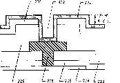
图4(A)为像素区域的俯视图,数字401指示的点线包围区域表示连接像素电极232和像素TFT的有源层204(确切地说,漏极区域216)的接触部分。另外,数字402指示一接触孔。4(A) is a top view of the pixel region, and the area surrounded by dotted lines indicated by
图4(B)为实施例2中接触部分401的局部放大图。数字204指有源层,数字205指门绝缘层,数字223指第一层间绝缘层,数字229指第二层间绝缘层。FIG. 4(B) is a partially enlarged view of the
实施例2的特点在于,其有源层204和像素电极232通过漏极228实现了电连接。The feature of Embodiment 2 is that the
根据本发明人的经验揭示出,在像素电极(例如,采用ITO(铟锡氧化物)膜)232和有源层(一般采用硅薄膜)204之间产生的接触电阻为非线性的,因而难于产生电阻接触。Reveal according to the inventor's experience, the contact resistance that produces between pixel electrode (for example, adopt ITO (Indium Tin Oxide) film) 232 and active layer (generally adopt silicon thin film) 204 is non-linear, thereby is difficult to Make resistive contact.
于是,形成由一导电膜,例如容易产生电阻接触的钛膜和铝膜的多层膜,来产生电阻接触的结构是有效的。附带地,本发明人研究发现,当铝膜和ITO膜彼此接触时,铝膜发生分解,因此根据实施例2,其所提供的导电膜结构为铝膜介于钛膜之间。Thus, it is effective to form a structure in which a resistive contact is made by a conductive film such as a multilayer film of a titanium film and an aluminum film which easily make a resistive contact. Incidentally, the inventors have found that when the aluminum film and the ITO film are in contact with each other, the aluminum film decomposes, so according to Example 2, the structure of the conductive film provided is that the aluminum film is interposed between the titanium films.
在此结构下,即使在接触孔402内引起磨擦损坏,漏极228也能达到与黑色基片中相近的效果。因此,即使产生畸变,也不会为肉眼识别。Under this structure, even if frictional damage is caused in the
根据本发明,当形成具有如图4(B)所示结构的接触部分时,有必要使阶梯形差别(对应于图4(B)中漏极228的膜厚)的高度限制在0.3μm或更小,如图4(B)所示。According to the present invention, when forming the contact portion with the structure shown in FIG. 4(B), it is necessary to limit the height of the step difference (corresponding to the film thickness of the
因此,在制作漏极228时,通过使其膜厚为0.3μm或更小,最好为0.25μm或更小,使其阶梯形差别限制在0.3μm或更小。Therefore, when the
根据实施例2,漏极228由多层膜制成,其材料主要成分为铝和钛膜,厚度控制为0.25μm。附带地,如果漏极228制成斜坡状,则阶梯形差别本身呈斜坡形,从而其上难于产生磨擦损坏。According to Embodiment 2, the
如上所述,根据实施例2中的结构,在接触部分附近产生的阶梯形差别高度为0.3μm或更小。因此,由于磨擦损坏或水平电场引起的畸变在接触部分的周围将不会发生。As described above, according to the structure in Embodiment 2, the height of the step-shaped difference generated in the vicinity of the contact portion is 0.3 μm or less. Therefore, distortion due to frictional damage or horizontal electric field will not occur around the contact portion.
根据本发明,在制作液晶显示装置时,其单元间距根据像素间距限定。特别地,单元间距限定为像素间距的十分之一或更小。According to the present invention, when manufacturing a liquid crystal display device, its cell pitch is defined according to the pixel pitch. In particular, the cell pitch is limited to one-tenth or less of the pixel pitch.
而且,在薄膜晶体管与像素电极之间的接触部分,使由结构原因引起的阶梯形差异为0.3μm或更小。Also, at the contact portion between the thin film transistor and the pixel electrode, the difference in the step shape due to the structure is made to be 0.3 μm or less.
根据上述本发明的结构可获得一高清晰度液晶显示装置,它不会产生如畸变等像差。According to the structure of the present invention as described above, a high-definition liquid crystal display device which does not generate aberrations such as distortion can be obtained.
例如,根据EWS(工程工作站)的说明,对角尺寸为2英寸的液晶显示装置,其像显示区域比率为5∶4(1280×1024像素),则其像素间距为约30μm。在此情况下,根据本发明,其单元间距应为3μm或更小,其阶梯形差别的高度应为0.3μm或更小,则不会产生畸变。For example, according to EWS (Engineering Workstation), a liquid crystal display device with a diagonal size of 2 inches has an image display area ratio of 5:4 (1280×1024 pixels), and its pixel pitch is about 30 μm. In this case, according to the present invention, the cell pitch should be 3 µm or less, and the height of the step-shaped difference should be 0.3 µm or less, so that distortion does not occur.
另外,本发明不仅适用于上述各例中的透射型液晶显示装置,也适用于反射型液晶显示装置。In addition, the present invention is applicable not only to the transmissive liquid crystal display devices in the above examples, but also to the reflective liquid crystal display devices.
Claims (16)
Applications Claiming Priority (3)
| Application Number | Priority Date | Filing Date | Title |
|---|---|---|---|
| JP115673/1996 | 1996-04-12 | ||
| JP115673/96 | 1996-04-12 | ||
| JP11567396AJPH09281508A (en) | 1996-04-12 | 1996-04-12 | Liquid crystal display device and its manufacture |
Related Child Applications (1)
| Application Number | Title | Priority Date | Filing Date |
|---|---|---|---|
| CNB021406286ADivisionCN1308745C (en) | 1996-04-12 | 1997-04-12 | Liquid crystal display device and manufacturing method thereof |
Publications (2)
| Publication Number | Publication Date |
|---|---|
| CN1172270Atrue CN1172270A (en) | 1998-02-04 |
| CN1161638C CN1161638C (en) | 2004-08-11 |
Family
ID=14668465
Family Applications (3)
| Application Number | Title | Priority Date | Filing Date |
|---|---|---|---|
| CNB021406286AExpired - LifetimeCN1308745C (en) | 1996-04-12 | 1997-04-12 | Liquid crystal display device and manufacturing method thereof |
| CNB2006101016765AExpired - LifetimeCN100464239C (en) | 1996-04-12 | 1997-04-12 | Liquid crystal display device and manufacturing method thereof |
| CNB971112851AExpired - LifetimeCN1161638C (en) | 1996-04-12 | 1997-04-12 | Display device and method for manufacturing the same |
Family Applications Before (2)
| Application Number | Title | Priority Date | Filing Date |
|---|---|---|---|
| CNB021406286AExpired - LifetimeCN1308745C (en) | 1996-04-12 | 1997-04-12 | Liquid crystal display device and manufacturing method thereof |
| CNB2006101016765AExpired - LifetimeCN100464239C (en) | 1996-04-12 | 1997-04-12 | Liquid crystal display device and manufacturing method thereof |
Country Status (5)
| Country | Link |
|---|---|
| US (4) | US6323932B1 (en) |
| JP (1) | JPH09281508A (en) |
| KR (2) | KR100328183B1 (en) |
| CN (3) | CN1308745C (en) |
| TW (1) | TW382073B (en) |
Cited By (1)
| Publication number | Priority date | Publication date | Assignee | Title |
|---|---|---|---|---|
| CN1322368C (en)* | 2004-04-14 | 2007-06-20 | 友达光电股份有限公司 | Pixel array of display and display including same |
Families Citing this family (80)
| Publication number | Priority date | Publication date | Assignee | Title |
|---|---|---|---|---|
| CN100341042C (en)* | 1997-02-17 | 2007-10-03 | 精工爱普生株式会社 | Display device |
| US6462722B1 (en)* | 1997-02-17 | 2002-10-08 | Seiko Epson Corporation | Current-driven light-emitting display apparatus and method of producing the same |
| JP3827806B2 (en)* | 1997-04-30 | 2006-09-27 | シャープ株式会社 | LCD panel |
| KR100223601B1 (en)* | 1997-05-29 | 1999-10-15 | 윤종용 | Lcd device |
| JP4105261B2 (en)* | 1997-08-20 | 2008-06-25 | 株式会社半導体エネルギー研究所 | Manufacturing method of electronic equipment |
| JP4094759B2 (en)* | 1999-02-05 | 2008-06-04 | 株式会社日立製作所 | Liquid crystal display |
| US7023021B2 (en)* | 2000-02-22 | 2006-04-04 | Semiconductor Energy Laboratory Co., Ltd. | Semiconductor device and method of manufacturing the same |
| JP2002072922A (en)* | 2000-06-13 | 2002-03-12 | Asahi Glass Co Ltd | Glass substrate for display and method for sorting the same |
| US7295509B2 (en) | 2000-09-13 | 2007-11-13 | Qualcomm, Incorporated | Signaling method in an OFDM multiple access system |
| US9130810B2 (en)* | 2000-09-13 | 2015-09-08 | Qualcomm Incorporated | OFDM communications methods and apparatus |
| US6636287B1 (en)* | 2001-02-28 | 2003-10-21 | Three-Five Systems, Inc. | Display systems with pixel electrodes at different distances from a control electrode |
| CN1298175C (en)* | 2001-07-06 | 2007-01-31 | 以克斯普雷有限公司 | Image projecting device and method |
| US20070047043A1 (en)* | 2002-07-08 | 2007-03-01 | Explay Ltd. | image projecting device and method |
| US20070003552A1 (en)* | 2002-07-09 | 2007-01-04 | Gebbink Martijn F B | Cross-beta structure comprising amyloid binding proteins and methods for detection of the cross-beta structure, for modulating cross-beta structures fibril formation and for modulating cross-beta structure-mediated toxicity and method for interfering with blood coagulation |
| US20040131559A1 (en)* | 2002-11-04 | 2004-07-08 | Hauck Douglas J. | Oral disease prevention and treatment |
| US7805220B2 (en) | 2003-03-14 | 2010-09-28 | Sharper Image Acquisition Llc | Robot vacuum with internal mapping system |
| US20050010331A1 (en)* | 2003-03-14 | 2005-01-13 | Taylor Charles E. | Robot vacuum with floor type modes |
| US7801645B2 (en)* | 2003-03-14 | 2010-09-21 | Sharper Image Acquisition Llc | Robotic vacuum cleaner with edge and object detection system |
| US20040244138A1 (en)* | 2003-03-14 | 2004-12-09 | Taylor Charles E. | Robot vacuum |
| US20040200505A1 (en)* | 2003-03-14 | 2004-10-14 | Taylor Charles E. | Robot vac with retractable power cord |
| US7058830B2 (en)* | 2003-03-19 | 2006-06-06 | International Business Machines Corporation | Power saving in a floating point unit using a multiplier and aligner bypass |
| US7286204B2 (en)* | 2003-03-28 | 2007-10-23 | Samsung Electronics Co., Ltd. | Spacers for display devices |
| US7382356B2 (en)* | 2003-09-15 | 2008-06-03 | Sharper Image Corp. | Input unit for games and musical keyboards |
| US20050100871A1 (en)* | 2003-11-10 | 2005-05-12 | Sharper Image Corporation | Training aid for physical movement with virtual work area |
| US20050099266A1 (en)* | 2003-11-10 | 2005-05-12 | Sharper Image Corporation | Motion detection for personal identification (biometric identification and detection-anti-terrorist) |
| TWI247935B (en)* | 2004-01-07 | 2006-01-21 | Shih-Hsien Tseng | Liquid crystal display device |
| US9137822B2 (en)* | 2004-07-21 | 2015-09-15 | Qualcomm Incorporated | Efficient signaling over access channel |
| US9148256B2 (en)* | 2004-07-21 | 2015-09-29 | Qualcomm Incorporated | Performance based rank prediction for MIMO design |
| KR100731733B1 (en)* | 2004-11-24 | 2007-06-22 | 삼성에스디아이 주식회사 | LCD and its manufacturing method |
| US20060203794A1 (en)* | 2005-03-10 | 2006-09-14 | Qualcomm Incorporated | Systems and methods for beamforming in multi-input multi-output communication systems |
| US9246560B2 (en)* | 2005-03-10 | 2016-01-26 | Qualcomm Incorporated | Systems and methods for beamforming and rate control in a multi-input multi-output communication systems |
| US9154211B2 (en)* | 2005-03-11 | 2015-10-06 | Qualcomm Incorporated | Systems and methods for beamforming feedback in multi antenna communication systems |
| US8446892B2 (en)* | 2005-03-16 | 2013-05-21 | Qualcomm Incorporated | Channel structures for a quasi-orthogonal multiple-access communication system |
| US20090213950A1 (en)* | 2005-03-17 | 2009-08-27 | Qualcomm Incorporated | Pilot signal transmission for an orthogonal frequency division wireless communication system |
| US9143305B2 (en)* | 2005-03-17 | 2015-09-22 | Qualcomm Incorporated | Pilot signal transmission for an orthogonal frequency division wireless communication system |
| US9461859B2 (en)* | 2005-03-17 | 2016-10-04 | Qualcomm Incorporated | Pilot signal transmission for an orthogonal frequency division wireless communication system |
| US9520972B2 (en)* | 2005-03-17 | 2016-12-13 | Qualcomm Incorporated | Pilot signal transmission for an orthogonal frequency division wireless communication system |
| US9184870B2 (en) | 2005-04-01 | 2015-11-10 | Qualcomm Incorporated | Systems and methods for control channel signaling |
| US9408220B2 (en)* | 2005-04-19 | 2016-08-02 | Qualcomm Incorporated | Channel quality reporting for adaptive sectorization |
| US9036538B2 (en) | 2005-04-19 | 2015-05-19 | Qualcomm Incorporated | Frequency hopping design for single carrier FDMA systems |
| US8879511B2 (en)* | 2005-10-27 | 2014-11-04 | Qualcomm Incorporated | Assignment acknowledgement for a wireless communication system |
| US8565194B2 (en) | 2005-10-27 | 2013-10-22 | Qualcomm Incorporated | Puncturing signaling channel for a wireless communication system |
| US8611284B2 (en)* | 2005-05-31 | 2013-12-17 | Qualcomm Incorporated | Use of supplemental assignments to decrement resources |
| US8462859B2 (en)* | 2005-06-01 | 2013-06-11 | Qualcomm Incorporated | Sphere decoding apparatus |
| US9179319B2 (en)* | 2005-06-16 | 2015-11-03 | Qualcomm Incorporated | Adaptive sectorization in cellular systems |
| US8599945B2 (en) | 2005-06-16 | 2013-12-03 | Qualcomm Incorporated | Robust rank prediction for a MIMO system |
| US8885628B2 (en) | 2005-08-08 | 2014-11-11 | Qualcomm Incorporated | Code division multiplexing in a single-carrier frequency division multiple access system |
| US9209956B2 (en)* | 2005-08-22 | 2015-12-08 | Qualcomm Incorporated | Segment sensitive scheduling |
| US20070041457A1 (en)* | 2005-08-22 | 2007-02-22 | Tamer Kadous | Method and apparatus for providing antenna diversity in a wireless communication system |
| US8644292B2 (en)* | 2005-08-24 | 2014-02-04 | Qualcomm Incorporated | Varied transmission time intervals for wireless communication system |
| US20070047495A1 (en)* | 2005-08-29 | 2007-03-01 | Qualcomm Incorporated | Reverse link soft handoff in a wireless multiple-access communication system |
| US9136974B2 (en)* | 2005-08-30 | 2015-09-15 | Qualcomm Incorporated | Precoding and SDMA support |
| US9210651B2 (en) | 2005-10-27 | 2015-12-08 | Qualcomm Incorporated | Method and apparatus for bootstraping information in a communication system |
| US9225488B2 (en) | 2005-10-27 | 2015-12-29 | Qualcomm Incorporated | Shared signaling channel |
| US9144060B2 (en) | 2005-10-27 | 2015-09-22 | Qualcomm Incorporated | Resource allocation for shared signaling channels |
| US8693405B2 (en)* | 2005-10-27 | 2014-04-08 | Qualcomm Incorporated | SDMA resource management |
| US8477684B2 (en) | 2005-10-27 | 2013-07-02 | Qualcomm Incorporated | Acknowledgement of control messages in a wireless communication system |
| US9225416B2 (en)* | 2005-10-27 | 2015-12-29 | Qualcomm Incorporated | Varied signaling channels for a reverse link in a wireless communication system |
| US8045512B2 (en) | 2005-10-27 | 2011-10-25 | Qualcomm Incorporated | Scalable frequency band operation in wireless communication systems |
| US9088384B2 (en)* | 2005-10-27 | 2015-07-21 | Qualcomm Incorporated | Pilot symbol transmission in wireless communication systems |
| US9172453B2 (en)* | 2005-10-27 | 2015-10-27 | Qualcomm Incorporated | Method and apparatus for pre-coding frequency division duplexing system |
| US8582509B2 (en)* | 2005-10-27 | 2013-11-12 | Qualcomm Incorporated | Scalable frequency band operation in wireless communication systems |
| US8582548B2 (en)* | 2005-11-18 | 2013-11-12 | Qualcomm Incorporated | Frequency division multiple access schemes for wireless communication |
| US8831607B2 (en)* | 2006-01-05 | 2014-09-09 | Qualcomm Incorporated | Reverse link other sector communication |
| US20070173355A1 (en)* | 2006-01-13 | 2007-07-26 | Klein William M | Wireless sensor scoring with automatic sensor synchronization |
| US20080015061A1 (en)* | 2006-07-11 | 2008-01-17 | Klein William M | Performance monitoring in a shooting sport using sensor synchronization |
| TWI545380B (en) | 2006-05-16 | 2016-08-11 | 半導體能源研究所股份有限公司 | Liquid crystal display device and semiconductor device |
| JP4774030B2 (en)* | 2007-02-19 | 2011-09-14 | セイコーエプソン株式会社 | Liquid crystal device and manufacturing method thereof, electronic device |
| US7998004B2 (en)* | 2008-01-24 | 2011-08-16 | Klein William M | Real-time wireless sensor scoring |
| JP5477612B2 (en)* | 2008-04-17 | 2014-04-23 | 株式会社ジャパンディスプレイ | Display device and electronic device |
| US8380531B2 (en)* | 2008-07-25 | 2013-02-19 | Invivodata, Inc. | Clinical trial endpoint development process |
| JP5525224B2 (en) | 2008-09-30 | 2014-06-18 | 株式会社半導体エネルギー研究所 | Display device |
| US20100232384A1 (en)* | 2009-03-13 | 2010-09-16 | Qualcomm Incorporated | Channel estimation based upon user specific and common reference signals |
| JP2012521339A (en)* | 2009-03-20 | 2012-09-13 | コーニング インコーポレイテッド | Precision laser marking |
| CN102483546B (en)* | 2009-09-08 | 2015-04-01 | 夏普株式会社 | Liquid crystal display device and manufacturing method thereof |
| CN102221761B (en)* | 2010-04-16 | 2014-04-02 | 中芯国际集成电路制造(上海)有限公司 | Silicon-based liquid crystal device and manufacturing method thereof |
| CN102629045B (en)* | 2011-06-17 | 2015-02-18 | 北京京东方光电科技有限公司 | Array substrate and liquid crystal display |
| KR101335527B1 (en)* | 2012-02-23 | 2013-12-02 | 엘지디스플레이 주식회사 | Organic Light Emitting Diode Display Device and Method for Manufacturing The Same |
| KR101970537B1 (en) | 2012-04-12 | 2019-04-22 | 삼성디스플레이 주식회사 | Display apparatus |
| JP6698321B2 (en) | 2014-12-02 | 2020-05-27 | 株式会社半導体エネルギー研究所 | Display device |
Family Cites Families (67)
| Publication number | Priority date | Publication date | Assignee | Title |
|---|---|---|---|---|
| JP3307150B2 (en)* | 1995-03-20 | 2002-07-24 | ソニー株式会社 | Active matrix display |
| DE6933214U (en) | 1969-08-22 | 1970-01-15 | E B Sport Internat Gmbh | EQUIPMENT ON CYCLING SHOES |
| JPS5495264A (en)* | 1978-01-11 | 1979-07-27 | Hitachi Ltd | Liquid crystal display element |
| US5365079A (en)* | 1982-04-30 | 1994-11-15 | Seiko Epson Corporation | Thin film transistor and display device including same |
| JPS61147232A (en)* | 1984-12-20 | 1986-07-04 | Canon Inc | liquid crystal element |
| DE3525618A1 (en) | 1985-07-18 | 1987-01-22 | Bosch Gmbh Robert | HEADLIGHTS FOR MOTOR VEHICLES |
| JPS6262334A (en)* | 1985-09-13 | 1987-03-19 | Canon Inc | Liquid crystal element |
| JPS62278537A (en) | 1986-05-27 | 1987-12-03 | Toshiba Corp | Display electrode array for active matrix display devices |
| JPS6370230A (en) | 1986-09-12 | 1988-03-30 | Toshiba Corp | Substrate for liquid crystal display device |
| JP2521752B2 (en) | 1987-05-11 | 1996-08-07 | 沖電気工業株式会社 | Liquid crystal display |
| US5327001A (en)* | 1987-09-09 | 1994-07-05 | Casio Computer Co., Ltd. | Thin film transistor array having single light shield layer over transistors and gate and drain lines |
| JPH0194316A (en) | 1987-10-07 | 1989-04-13 | Matsushita Electric Ind Co Ltd | liquid crystal display element |
| JPH01219824A (en)* | 1988-02-29 | 1989-09-01 | Seikosha Co Ltd | Amorphous silicon thin film transistor array substrate |
| EP0378293B1 (en)* | 1989-01-09 | 1994-09-14 | Matsushita Electric Industrial Co., Ltd. | Liquid crystal display device and its driving method |
| US5151807A (en)* | 1989-01-31 | 1992-09-29 | Sharp Kabushiki Kaisha | Active matrix substrate and active matrix display apparatus |
| JP2746403B2 (en)* | 1989-02-13 | 1998-05-06 | コニカ株式会社 | Liquid crystal display device and manufacturing method thereof |
| JPH03111820A (en) | 1989-09-26 | 1991-05-13 | Sony Corp | Liquid crystal display element |
| JP2961786B2 (en) | 1990-02-22 | 1999-10-12 | セイコーエプソン株式会社 | Liquid crystal display |
| JPH0431826A (en) | 1990-05-29 | 1992-02-04 | Alps Electric Co Ltd | Liquid crystal display element |
| JPH0437726A (en) | 1990-06-01 | 1992-02-07 | Oki Electric Ind Co Ltd | Liquid crystal display device |
| US5426526A (en) | 1991-04-05 | 1995-06-20 | Sharp Kabushiki Kaisha | Reflection type single crystal silicon substrate liquid crystal display device and system |
| JP2804198B2 (en) | 1991-04-05 | 1998-09-24 | シャープ株式会社 | Liquid crystal display |
| JPH04323625A (en) | 1991-04-23 | 1992-11-12 | Sony Corp | Liquid crystal display device |
| JPH0534720A (en) | 1991-07-29 | 1993-02-12 | Toshiba Corp | Active matrix liquid crystal display device |
| JPH05142548A (en)* | 1991-11-21 | 1993-06-11 | Matsushita Electric Ind Co Ltd | LCD display panel |
| JPH05249478A (en)* | 1991-12-25 | 1993-09-28 | Toshiba Corp | Liquid crystal display device |
| JPH06194687A (en)* | 1992-10-30 | 1994-07-15 | Nec Corp | Transmission type active matrix liquid crystal element |
| JPH05323370A (en) | 1992-05-20 | 1993-12-07 | Matsushita Electric Ind Co Ltd | Active matrix type liquid crystal display element |
| JP2818335B2 (en)* | 1992-05-22 | 1998-10-30 | シャープ株式会社 | Liquid crystal device, display device, photodetector, color copier, printing plate making device, image input / output device, image operation device, lighting device, and method of manufacturing liquid crystal device |
| US5499127A (en)* | 1992-05-25 | 1996-03-12 | Sharp Kabushiki Kaisha | Liquid crystal display device having a larger gap between the substrates in the display area than in the sealant area |
| JPH05323301A (en)* | 1992-05-25 | 1993-12-07 | Ricoh Co Ltd | Liquid crystal display element |
| JPH0695153A (en) | 1992-09-17 | 1994-04-08 | Seiko Epson Corp | Active matrix liquid crystal display |
| JP3615556B2 (en) | 1992-11-04 | 2005-02-02 | セイコーエプソン株式会社 | Active matrix substrate and manufacturing method thereof |
| US5583671A (en)* | 1992-11-09 | 1996-12-10 | Casio Computer Co., Ltd. | Method of manufacturing polymer dispersed liquid crystal display devices |
| JP3338493B2 (en)* | 1992-12-17 | 2002-10-28 | ソニー株式会社 | Liquid crystal display device and information processing device |
| JP3383047B2 (en) | 1992-12-25 | 2003-03-04 | ソニー株式会社 | Active matrix substrate |
| JPH0720481A (en) | 1993-07-05 | 1995-01-24 | Sony Corp | Active matrix liquid crystal display device |
| JPH0720497A (en) | 1993-07-05 | 1995-01-24 | Sony Corp | Active matrix liquid crystal display device |
| JPH0720496A (en) | 1993-06-30 | 1995-01-24 | Sony Corp | Active matrix type liquid crystal display device |
| DE69332142T2 (en) | 1992-12-25 | 2003-03-06 | Sony Corp., Tokio/Tokyo | Active matrix substrate |
| GB2274922B (en) | 1993-01-21 | 1996-10-23 | Sharp Kk | Liquid crystal projector |
| US5843225A (en) | 1993-02-03 | 1998-12-01 | Semiconductor Energy Laboratory Co., Ltd. | Process for fabricating semiconductor and process for fabricating semiconductor device |
| JPH06250224A (en) | 1993-02-24 | 1994-09-09 | Sony Corp | Liquid crystal display device |
| JP3410754B2 (en) | 1993-03-01 | 2003-05-26 | セイコーエプソン株式会社 | Liquid crystal display |
| JPH06258661A (en) | 1993-03-02 | 1994-09-16 | Seiko Epson Corp | Liquid crystal display |
| JP3413230B2 (en)* | 1993-03-02 | 2003-06-03 | セイコーエプソン株式会社 | Liquid crystal display |
| JPH06308505A (en)* | 1993-04-23 | 1994-11-04 | Seiko Instr Inc | Liquid crystal electrooptical device |
| US5502583A (en)* | 1993-05-15 | 1996-03-26 | Nec Corporation | Liquid crystal display device capable of compensating for a positioning error between a drain line and a display electrode |
| JP2556253B2 (en)* | 1993-05-25 | 1996-11-20 | 日本電気株式会社 | Liquid crystal display |
| US5895933A (en) | 1993-06-25 | 1999-04-20 | Semiconductor Energy Laboratory Co., Ltd. | Semiconductor device and method for its preparation |
| EP0637771B1 (en)* | 1993-08-04 | 2001-07-11 | Matsushita Electric Industrial Co., Ltd. | Method of producing a liquid crystal display apparatus having a random orientation alignment film |
| JPH07120784A (en)* | 1993-10-22 | 1995-05-12 | Rohm Co Ltd | Liquid crystal display device and its production |
| JPH07140479A (en)* | 1993-11-22 | 1995-06-02 | Fujitsu Ltd | LCD unit |
| JPH07181438A (en) | 1993-12-24 | 1995-07-21 | Sharp Corp | Liquid crystal display device and defect correcting method thereof |
| JPH07248507A (en)* | 1994-03-10 | 1995-09-26 | Matsushita Electron Corp | Liquid crystal display device |
| KR0130372B1 (en) | 1994-06-17 | 1998-04-09 | 구자홍 | Manufacturing method of liquid crystal display device |
| JPH0854648A (en)* | 1994-08-10 | 1996-02-27 | Toshiba Corp | Liquid crystal display |
| JPH0862639A (en)* | 1994-08-26 | 1996-03-08 | Seiko Epson Corp | Liquid crystal device |
| JPH08122768A (en)* | 1994-10-19 | 1996-05-17 | Sony Corp | Display device |
| US5757456A (en) | 1995-03-10 | 1998-05-26 | Semiconductor Energy Laboratory Co., Ltd. | Display device and method of fabricating involving peeling circuits from one substrate and mounting on other |
| JP3292657B2 (en)* | 1995-04-10 | 2002-06-17 | キヤノン株式会社 | Thin film transistor and method for manufacturing liquid crystal display device using the same |
| JPH0926603A (en)* | 1995-05-08 | 1997-01-28 | Semiconductor Energy Lab Co Ltd | Display device |
| US6372534B1 (en) | 1995-06-06 | 2002-04-16 | Lg. Philips Lcd Co., Ltd | Method of making a TFT array with photo-imageable insulating layer over address lines |
| US5699139A (en)* | 1995-07-05 | 1997-12-16 | Minnesota Mining And Manufacturing Company | Liquid crystal device having pressure relief structure |
| US6067137A (en)* | 1995-08-25 | 2000-05-23 | Kuraray Co., Ltd. | Image display apparatus with hydrophobic diffraction grating for an enlarged viewing angle |
| KR0171102B1 (en)* | 1995-08-29 | 1999-03-20 | 구자홍 | LCD Structure and Manufacturing Method |
| JP2728059B2 (en) | 1995-10-06 | 1998-03-18 | 日本電気株式会社 | Reflective liquid crystal display |
- 1996
- 1996-04-12JPJP11567396Apatent/JPH09281508A/ennot_activeWithdrawn
- 1997
- 1997-04-10TWTW086104601Apatent/TW382073B/ennot_activeIP Right Cessation
- 1997-04-11USUS08/835,725patent/US6323932B1/ennot_activeExpired - Lifetime
- 1997-04-12CNCNB021406286Apatent/CN1308745C/ennot_activeExpired - Lifetime
- 1997-04-12CNCNB2006101016765Apatent/CN100464239C/ennot_activeExpired - Lifetime
- 1997-04-12KRKR1019970013537Apatent/KR100328183B1/ennot_activeExpired - Lifetime
- 1997-04-12CNCNB971112851Apatent/CN1161638C/ennot_activeExpired - Lifetime
- 2001
- 2001-07-24KRKR1020010044394Apatent/KR100349022B1/ennot_activeExpired - Lifetime
- 2001-09-24USUS09/969,268patent/US7095478B2/ennot_activeExpired - Fee Related
- 2006
- 2006-03-20USUS11/276,977patent/US7196749B2/ennot_activeExpired - Fee Related
- 2007
- 2007-03-23USUS11/690,183patent/US7636136B2/ennot_activeExpired - Fee Related
Cited By (1)
| Publication number | Priority date | Publication date | Assignee | Title |
|---|---|---|---|---|
| CN1322368C (en)* | 2004-04-14 | 2007-06-20 | 友达光电股份有限公司 | Pixel array of display and display including same |
Also Published As
| Publication number | Publication date |
|---|---|
| CN1161638C (en) | 2004-08-11 |
| JPH09281508A (en) | 1997-10-31 |
| US6323932B1 (en) | 2001-11-27 |
| CN1952763A (en) | 2007-04-25 |
| US20060146266A1 (en) | 2006-07-06 |
| US20020018157A1 (en) | 2002-02-14 |
| US7636136B2 (en) | 2009-12-22 |
| KR100349022B1 (en) | 2002-08-17 |
| US7095478B2 (en) | 2006-08-22 |
| CN1474218A (en) | 2004-02-11 |
| TW382073B (en) | 2000-02-11 |
| CN1308745C (en) | 2007-04-04 |
| US20070177068A1 (en) | 2007-08-02 |
| US7196749B2 (en) | 2007-03-27 |
| CN100464239C (en) | 2009-02-25 |
| KR100328183B1 (en) | 2002-11-30 |
Similar Documents
| Publication | Publication Date | Title |
|---|---|---|
| CN1161638C (en) | Display device and method for manufacturing the same | |
| CN1178098C (en) | Liquid crystal display device | |
| CN1267783C (en) | Liquid crystal display device | |
| CN1232869C (en) | Electrooptical device and electronic instrument | |
| CN100335957C (en) | In-plane switching mode liquid crystal display device and method for fabricating the same | |
| CN1257428C (en) | Electro-optical device, manufacturing method thereof, and electronic device | |
| CN1222815C (en) | Semipermeability reflecting liquid crystal device and electronic equipment using it | |
| CN1099612C (en) | Method for manufacturing electrical optical elements | |
| CN1143169C (en) | Liquid crystal display element with controlled storage capacitance | |
| CN100350319C (en) | Liquid crystal display panel and fabricating method thereof | |
| CN1224859C (en) | Semipermeability reflecting liquid crystal device and electronic equipment using it | |
| CN1721934A (en) | Liquid crystal display device and image display device | |
| CN1132384A (en) | Display device and method for driving the same | |
| CN1945398A (en) | Liquid crystal display panel and method for fabricating the same | |
| CN1819217A (en) | Active matrix substrate and its manufacturing method | |
| CN1913155A (en) | Liquid crystal display device and method for manufacturing the same | |
| CN1201183C (en) | Electrooptical device and mfg. method electronic apparatus | |
| CN1758120A (en) | LCD and display board thereof | |
| CN1625713A (en) | Multi-domain liquid crystal display and its thin film transistor substrate | |
| CN1292302C (en) | Electro-optic panel and manufacturing method thereof | |
| CN101055393A (en) | Liquid crystal display and its manufacture method | |
| CN1797156A (en) | Liquid crystal display device and method for fabricating the same | |
| CN1485667A (en) | Substrate for liquid crystal display device and liquid crystal display device having same | |
| CN1933165A (en) | Array substrate, liquid crystal display panel and liquid crystal display device having the same | |
| CN1231803C (en) | Reflection electrooptical device and electronic equipment |
Legal Events
| Date | Code | Title | Description |
|---|---|---|---|
| C06 | Publication | ||
| PB01 | Publication | ||
| C10 | Entry into substantive examination | ||
| SE01 | Entry into force of request for substantive examination | ||
| C14 | Grant of patent or utility model | ||
| GR01 | Patent grant | ||
| CX01 | Expiry of patent term | Granted publication date:20040811 | |
| CX01 | Expiry of patent term |