CN116435872A - A Narrow Linewidth Spectral Beam Combining Device for Arrayed Semiconductor Lasers - Google Patents
A Narrow Linewidth Spectral Beam Combining Device for Arrayed Semiconductor LasersDownload PDFInfo
- Publication number
- CN116435872A CN116435872ACN202310216585.XACN202310216585ACN116435872ACN 116435872 ACN116435872 ACN 116435872ACN 202310216585 ACN202310216585 ACN 202310216585ACN 116435872 ACN116435872 ACN 116435872A
- Authority
- CN
- China
- Prior art keywords
- semiconductor lasers
- diffraction grating
- axis
- beam combining
- narrow
- Prior art date
- Legal status (The legal status is an assumption and is not a legal conclusion. Google has not performed a legal analysis and makes no representation as to the accuracy of the status listed.)
- Granted
Links
Images


Classifications
- H—ELECTRICITY
- H01—ELECTRIC ELEMENTS
- H01S—DEVICES USING THE PROCESS OF LIGHT AMPLIFICATION BY STIMULATED EMISSION OF RADIATION [LASER] TO AMPLIFY OR GENERATE LIGHT; DEVICES USING STIMULATED EMISSION OF ELECTROMAGNETIC RADIATION IN WAVE RANGES OTHER THAN OPTICAL
- H01S5/00—Semiconductor lasers
- H01S5/40—Arrangement of two or more semiconductor lasers, not provided for in groups H01S5/02 - H01S5/30
- H01S5/4012—Beam combining, e.g. by the use of fibres, gratings, polarisers, prisms
- H—ELECTRICITY
- H01—ELECTRIC ELEMENTS
- H01S—DEVICES USING THE PROCESS OF LIGHT AMPLIFICATION BY STIMULATED EMISSION OF RADIATION [LASER] TO AMPLIFY OR GENERATE LIGHT; DEVICES USING STIMULATED EMISSION OF ELECTROMAGNETIC RADIATION IN WAVE RANGES OTHER THAN OPTICAL
- H01S5/00—Semiconductor lasers
- H01S5/40—Arrangement of two or more semiconductor lasers, not provided for in groups H01S5/02 - H01S5/30
- H01S5/4025—Array arrangements, e.g. constituted by discrete laser diodes or laser bar
- Y—GENERAL TAGGING OF NEW TECHNOLOGICAL DEVELOPMENTS; GENERAL TAGGING OF CROSS-SECTIONAL TECHNOLOGIES SPANNING OVER SEVERAL SECTIONS OF THE IPC; TECHNICAL SUBJECTS COVERED BY FORMER USPC CROSS-REFERENCE ART COLLECTIONS [XRACs] AND DIGESTS
- Y02—TECHNOLOGIES OR APPLICATIONS FOR MITIGATION OR ADAPTATION AGAINST CLIMATE CHANGE
- Y02A—TECHNOLOGIES FOR ADAPTATION TO CLIMATE CHANGE
- Y02A90/00—Technologies having an indirect contribution to adaptation to climate change
- Y02A90/10—Information and communication technologies [ICT] supporting adaptation to climate change, e.g. for weather forecasting or climate simulation
Landscapes
- Physics & Mathematics (AREA)
- Condensed Matter Physics & Semiconductors (AREA)
- General Physics & Mathematics (AREA)
- Electromagnetism (AREA)
- Optics & Photonics (AREA)
- Semiconductor Lasers (AREA)
Abstract
Description
Translated fromChinese技术领域technical field
本发明涉及半导体激光技术领域,具体涉及一种阵列半导体激光器的窄线宽光谱合束装置。The invention relates to the technical field of semiconductor lasers, in particular to a narrow-linewidth spectral beam combining device for an array semiconductor laser.
背景技术Background technique
半导体激光器具有效率高、体积小、寿命长、波长丰富和可以直接电驱动等诸多优点,但其光束质量以及单个发光单元输出功率极大限制了它的应用领域。而外腔反馈光谱合束是一种提高阵列半导体激光器亮度和光束质量的有效方法,极大提高了半导体激光器的性能。Semiconductor lasers have many advantages such as high efficiency, small size, long life, rich wavelengths, and direct electrical drive, but their beam quality and output power of a single light-emitting unit greatly limit its application fields. External cavity feedback spectral beam combining is an effective method to improve the brightness and beam quality of arrayed semiconductor lasers, which greatly improves the performance of semiconductor lasers.
外腔光谱合束实现多路激光在近场和远场同时空间重叠,合成至单一孔径输出的激光,合束后整体的光束质量和单个发光单元接近,输出功率是单个发光单元的N倍。但由于光栅的色散和外腔反馈的作用,使得各个激光单元起振在不同波长,导致合束后的整体线宽展宽。因此,阵列半导体激光器的光谱合束技术在泵浦激光器等一些要求窄线宽的领域应用非常受限。The external cavity spectral beam combination realizes the spatial overlap of multiple lasers in the near field and far field at the same time, and synthesizes the laser output into a single aperture. After the beam combination, the overall beam quality is close to that of a single light-emitting unit, and the output power is N times that of a single light-emitting unit. However, due to the dispersion of the grating and the feedback of the external cavity, each laser unit oscillates at different wavelengths, resulting in broadening of the overall linewidth after beam combining. Therefore, the spectral beam combining technology of arrayed semiconductor lasers is very limited in some fields requiring narrow linewidths such as pump lasers.
通常高功率的光谱合束输出需要多个阵列半导体激光参与合束,但是单个阵列半导体激光器光谱合束后输出光束的整体线宽,决定了能够参与光谱合束的阵列半导体激光器个数。而且整体线宽随着参与光谱合束的阵列半导体激光器个数增加而增大,若单个阵列半导体激光器的光谱合束线宽太宽,则增益带宽允许参与光谱合束的半导体激光阵列的个数就会下降。同时光栅的高衍射效率只存在一定波长范围,参与光谱合束的阵列半导体激光器个数增加的越多,则偏离光栅最大衍射效率的波长越远,整体的光谱合束效率就会降低。如果以牺牲效率来换取多个阵列半导体激光器的光谱合束,那样半导体激光器高转换效率的优势将得不到体现。因此,实现单个阵列半导体激光器光谱合束后的窄线宽输出,成为实现多个阵列半导体激光器光谱合束的关键。Usually high-power spectral beam combining output requires multiple array semiconductor lasers to participate in beam combining, but the overall linewidth of the output beam after spectral combining of a single array semiconductor laser determines the number of array semiconductor lasers that can participate in spectral beam combining. Moreover, the overall linewidth increases as the number of array semiconductor lasers participating in spectral beam combining increases. If the spectral beam combining linewidth of a single array semiconductor laser is too wide, the gain bandwidth allows the number of semiconductor laser arrays participating in spectral beam combining. will drop. At the same time, the high diffraction efficiency of the grating only exists in a certain wavelength range. The more the number of array semiconductor lasers participating in the spectral beam combining increases, the farther the wavelength deviates from the maximum diffraction efficiency of the grating, and the overall spectral beam combining efficiency will decrease. If efficiency is sacrificed in exchange for spectral beam combining of multiple array semiconductor lasers, the advantages of high conversion efficiency of semiconductor lasers will not be reflected. Therefore, realizing the narrow linewidth output after spectral combining of a single array of semiconductor lasers has become the key to realizing the spectral combining of multiple arrays of semiconductor lasers.
目前,为了获得窄线宽光谱合束输出,一般采用长焦距传输透镜、高刻线密度衍射光栅以及光栅对等方法来压缩光谱线宽,但这些方法都会造成外腔长度大幅增加、合束效率下降、成本增高等负面影响。At present, in order to obtain narrow linewidth spectral beam combining output, methods such as long focal length transmission lens, high-line density diffraction grating and grating pair are generally used to compress the spectral linewidth, but these methods will cause a large increase in the length of the external cavity and reduce the beam combining efficiency. Negative effects such as decline and cost increase.
发明内容Contents of the invention
针对现有技术中存在的不足之处,本发明提供一种阵列半导体激光器的窄线宽光谱合束装置;其通过在外腔中引入斜方棱镜组合,对阵列半导体激光器出射的光束进行分割重排,将光谱合束方向的光束宽度缩短2/3左右,进而有效的将光谱合束线宽压缩2/3左右,为实现阵列半导体激光器的光谱合束线宽窄化以及系统小型化提供一种新方案。Aiming at the deficiencies in the prior art, the present invention provides a narrow-linewidth spectral beam combining device for array semiconductor lasers; it divides and rearranges the light beams emitted by array semiconductor lasers by introducing a combination of rhombic prisms into the external cavity , shorten the beam width in the direction of spectral beam combining by about 2/3, and then effectively compress the spectral beam combining line width by about 2/3, providing a new method for realizing the narrowing of spectral beam combining line width and system miniaturization of array semiconductor lasers plan.
本发明公开了一种阵列半导体激光器的窄线宽光谱合束装置,包括:沿激光传输方向依次设置的阵列半导体激光器、快轴准直镜、慢轴准直镜、斜方棱镜组合、柱面传输透镜、衍射光栅和输出耦合镜;The invention discloses a narrow-linewidth spectral beam combining device of an array semiconductor laser, comprising: an array semiconductor laser arranged in sequence along the laser transmission direction, a fast-axis collimator, a slow-axis collimator, a combination of orthorhombic prisms, and a cylinder Transfer lenses, diffraction gratings and output coupling mirrors;
所述阵列半导体激光器和衍射光栅分别位于柱面传输透镜的前后焦平面上,所述输出耦合镜放置在所述衍射光栅的-1级衍射光输出方向且与-1级衍射光垂直;The array semiconductor laser and the diffraction grating are respectively located on the front and rear focal planes of the cylindrical transmission lens, and the output coupling mirror is placed in the output direction of the -1 order diffracted light of the diffraction grating and is perpendicular to the -1 order diffracted light;
所述斜方棱镜组合对所述阵列半导体激光器出射的慢轴方向光束进行分割重排,所述慢轴方向为光谱合束方向;一排光束经过两组斜方棱镜分割重排后,转换为在快轴方向上等距排列的多部分光束,将慢轴方向光束宽度缩短2/3;所述柱面传输透镜将多部分光束转换为不同角度入射至衍射光栅上,经所述衍射光栅衍射后入射至所述输出耦合镜。The combination of rhombic prisms divides and rearranges the light beams in the direction of the slow axis emitted by the array semiconductor laser, and the direction of the slow axis is the beam combining direction of the spectrum; The multi-part beams arranged equidistantly in the fast axis direction shorten the beam width in the slow axis direction by 2/3; the cylindrical transmission lens converts the multi-part beams into different angles and enters the diffraction grating, which is diffracted by the diffraction grating post-incidence to the output coupler mirror.
作为本发明的进一步改进,所述斜方棱镜组合包含两组;As a further improvement of the present invention, the rhombic prism combination includes two groups;
第一组包含在慢轴方向平行放置的多片斜方棱镜,用于将所述阵列半导体激光器出射的慢轴方向光束分割为多部分,相对于中间部分光束,一侧光束向上偏移,另一侧光束向下偏移,两侧偏移量相等;The first group includes a plurality of rhombic prisms placed in parallel in the direction of the slow axis, which are used to divide the light beam in the direction of the slow axis emitted by the array semiconductor laser into multiple parts. The beam on one side is offset downwards, and the offset on both sides is equal;
第二组包含在快轴方向交错放置多片斜方棱镜,将两侧光束在慢轴方向发生等距位移,两侧光束的出射位置与中间光束在快轴方向上重合;The second group includes multiple rhombic prisms staggered in the direction of the fast axis, and the beams on both sides are displaced equidistantly in the direction of the slow axis, and the exit positions of the beams on both sides coincide with the middle beam in the direction of the fast axis;
所述阵列半导体激光器出射的一排慢轴方向上的光束经过两组斜方棱镜分割重排后,转换为在快轴方向上等距排列的多部分光束。A row of light beams in the direction of the slow axis emitted by the array semiconductor lasers are divided and rearranged by two sets of rhombic prisms, and converted into multi-part light beams arranged equidistantly in the direction of the fast axis.
更进一步,第一组和第二组均包含三片斜方棱镜,所述阵列半导体激光器出射的一排慢轴方向上的光束经过两组斜方棱镜分割重排后,转换为在快轴方向上等距排列的三部分光束,此时慢轴方向的光束宽度相对于原先缩短了2/3左右。Furthermore, the first group and the second group both contain three pieces of rhomboidal prisms, and a row of light beams emitted by the array semiconductor laser in the direction of the slow axis are divided and rearranged by two groups of rhombic prisms, and then converted into beams in the direction of the fast axis The three beams arranged equidistantly above, the beam width in the slow axis direction is shortened by about 2/3 compared with the original one.
作为本发明的进一步改进,所述斜方棱镜的通光面均镀增透膜,透过率≥99%。As a further improvement of the present invention, the light-transmitting surface of the rhomboid prism is coated with an anti-reflection film, and the transmittance is ≥ 99%.
作为本发明的进一步改进,所述阵列半导体激光器的前腔面镀增透膜,透过率≥99%,以减少内腔反馈的影响,更好的实现外腔波长锁定;所述阵列半导体激光器包括但不限于线阵半导体激光器和叠阵半导体激光器中的一种。As a further improvement of the present invention, the front cavity surface of the array semiconductor laser is coated with an anti-reflection film, and the transmittance is ≥ 99%, so as to reduce the influence of inner cavity feedback and better achieve external cavity wavelength locking; the array semiconductor laser Including but not limited to one of linear array semiconductor lasers and stacked semiconductor lasers.
作为本发明的进一步改进,所述快轴准直镜为柱面微透镜,所述慢轴准直镜为柱面微透镜阵列;所述快轴准直镜和慢轴准直镜的通光面均镀增透膜,透过率≥99%;快轴准直镜、慢轴准直镜分别对线阵半导体激光器输出激光的快慢轴进行准直,以降低光束发散角。As a further improvement of the present invention, the fast-axis collimator is a cylindrical microlens, and the slow-axis collimator is a cylindrical microlens array; the light transmission of the fast-axis collimator and the slow-axis collimator The surface is coated with anti-reflection coating, and the transmittance is ≥99%. The fast axis collimator and the slow axis collimator respectively collimate the fast and slow axes of the output laser light of the linear array semiconductor laser to reduce the beam divergence angle.
作为本发明的进一步改进,在所述光谱合束方向上,所述柱面传输透镜将所述斜方棱镜组合分割重排后的光束叠加到衍射光栅上,通光面镀增透膜,透过率≥99%。As a further improvement of the present invention, in the spectral beam combining direction, the cylindrical transmission lens superimposes the light beams split and rearranged by the combination of the rhomboid prisms on the diffraction grating, and the transparent surface is coated with an anti-reflective coating, and the transparent Pass rate ≥ 99%.
作为本发明的进一步改进,所述衍射光栅与光轴按Littrow角放置,所述阵列半导体激光器的光束偏振方向与所述衍射光栅的衍射偏振方向匹配,以达到高衍射效率;所述衍射光栅包括但不限于反射式衍射光栅和透射式衍射光栅中的一种。As a further improvement of the present invention, the diffraction grating and the optical axis are placed at a Littrow angle, and the beam polarization direction of the array semiconductor laser matches the diffraction polarization direction of the diffraction grating to achieve high diffraction efficiency; the diffraction grating includes But not limited to one of reflective diffraction grating and transmissive diffraction grating.
作为本发明的进一步改进,所述输出耦合镜将部分比例的-1级衍射光束反馈回原发光单元实现波长锁定,剩余比例的光束作为输出光束出射。与现有技术相比,本发明的有益效果为:As a further improvement of the present invention, the output coupling mirror feeds back part of the -1st order diffracted beam to the original light emitting unit to achieve wavelength locking, and the remaining proportion of the beam is output as the output beam. Compared with prior art, the beneficial effect of the present invention is:
本发明的光谱合束装置可以在采用短焦距的柱面传输透镜的情况下实现窄线宽光谱合束输出,极大缩短了合束结构的外腔长度,提高了合束结构的可靠性和稳定性。The spectral beam combining device of the present invention can realize narrow-linewidth spectral beam combining output under the condition of adopting a cylindrical transmission lens with a short focal length, which greatly shortens the length of the external cavity of the beam combining structure, and improves the reliability and reliability of the beam combining structure. stability.
附图说明Description of drawings
为了更清楚地说明本发明实施例或现有技术中的技术方案,下面将对实施例或现有技术描述中所需要使用的附图作简单的介绍,应当理解,以下附图仅示出了本申请的某些实施例,显然,所描述的实施例是本发明的一部分实施例,而不是全部的实施例。因此不应被看作是对范围的限定,对于本领域普通技术人员来讲,在不付出创造性劳动的前提下,还可以根据这些附图获得其他的附图。In order to more clearly illustrate the technical solutions in the embodiments of the present invention or the prior art, the following will briefly introduce the drawings that need to be used in the description of the embodiments or the prior art. It should be understood that the following drawings only show Certain embodiments of the present application, obviously, the described embodiments are part of the embodiments of the present invention, but not all of the embodiments. Therefore, it should not be regarded as a limitation on the scope. For those skilled in the art, other drawings can also be obtained according to these drawings without creative work.
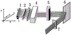
图1为本发明实施例1的线阵半导体激光器的窄线宽光谱合束装置的立体示意图;Fig. 1 is the three-dimensional schematic diagram of the narrow linewidth spectral beam combining device of the linear array semiconductor laser of
图2为本发明实施例1的线阵半导体激光器的窄线宽光谱合束装置的俯视图;2 is a top view of a narrow linewidth spectral beam combining device of a linear array semiconductor laser according to
图3为本发明实施例1中斜方棱镜组合的光束分割重排立体示意图;3 is a three-dimensional schematic diagram of beam splitting and rearranging of a combination of rhombic prisms in
图4为本发明实施例1中斜方棱镜组合的光束分割重排正视示意图;Fig. 4 is a schematic front view of beam splitting and rearranging of the combination of rhombic prisms in
图5为本发明实施例1的线阵半导体激光器的窄线宽光谱合束装置中光斑变化示意图;5 is a schematic diagram of spot changes in the narrow linewidth spectral beam combining device of the linear array semiconductor laser according to
图6为本发明实施例2的叠阵半导体激光器的窄线宽光谱合束装置的立体示意图;6 is a schematic perspective view of a narrow linewidth spectral beam combining device of a stacked semiconductor laser according to
图7为本发明实施例2的叠阵半导体激光器的窄线宽光谱合束装置中光斑变化示意图。FIG. 7 is a schematic diagram of light spot changes in the narrow linewidth spectral beam combining device of the stacked semiconductor laser according to
图中:In the picture:
1、线阵半导体激光器或叠阵半导体激光器;2、快轴准直镜;3、慢轴准直镜;4、斜方棱镜组合;5、柱面传输透镜;6、衍射光栅;7、输出耦合镜。1. Linear array semiconductor laser or stacked array semiconductor laser; 2. Fast axis collimator; 3. Slow axis collimator; 4. Rhombic prism combination; 5. Cylindrical transmission lens; 6. Diffraction grating; 7. Output coupling mirror.
具体实施方式Detailed ways
为使本发明实施例的目的、技术方案和优点更加清楚,下面将结合本发明实施例中的附图,对本发明实施例中的技术方案进行清楚、完整地描述,显然,所描述的实施例是本发明的一部分实施例,而不是全部的实施例。基于本发明中的实施例,本领域普通技术人员在没有做出创造性劳动的前提下所获得的所有其他实施例,都属于本发明保护的范围。In order to make the purpose, technical solutions and advantages of the embodiments of the present invention clearer, the technical solutions in the embodiments of the present invention will be clearly and completely described below in conjunction with the drawings in the embodiments of the present invention. Obviously, the described embodiments It is a part of embodiments of the present invention, but not all embodiments. Based on the embodiments of the present invention, all other embodiments obtained by persons of ordinary skill in the art without making creative efforts belong to the protection scope of the present invention.
下面结合附图对本发明做进一步的详细描述:Below in conjunction with accompanying drawing, the present invention is described in further detail:
实施例1Example 1
如图1、2所示,本发明提供一种线阵半导体激光器的窄线宽光谱合束装置,具体包括:线阵半导体激光器1、快轴准直镜2、慢轴准直镜3、斜方棱镜组合4、柱面传输透镜5、衍射光栅6以及输出耦合镜7;沿线阵半导体激光器1的光轴依次设置快轴准直镜2、慢轴准直镜3、斜方棱镜组合4、柱面传输透镜5和衍射光栅6,输出耦合镜7放置在衍射光栅6的-1级衍射光输出方向,并与-1级衍射光垂直。光谱合束方向为慢轴方向,沿水平方向(x轴)。As shown in Figures 1 and 2, the present invention provides a narrow-linewidth spectral beam combining device for a linear array semiconductor laser, which specifically includes: a linear
本实施例中:In this example:
线阵半导体激光器1的慢轴方向沿水平方向(x轴),快轴方向垂直于水平方向(y轴),其前腔面镀增透膜,透过率≥99%。The slow axis direction of the linear
快轴准直镜2和慢轴准直镜3的通光面镀增透膜,透过率≥99%,用于准直线阵半导体激光器1出射的激光,降低光束发散角。The light-transmitting surfaces of the fast-
斜方棱镜组合4置于线阵半导体激光器1与柱面传输透镜5之间;斜方棱镜组合4对线阵半导体激光器1出射的慢轴方向光束进行分割重排,一排光束经过两组斜方棱镜分割重排后,转换为在快轴方向上等距排列的三部分光束,将慢轴方向光束宽度缩短2/3左右;斜方棱镜组合4的通光面均镀增透膜,透过率≥99%。The
柱面传输透镜5的通光面镀增透膜,透过率≥99%,距离线阵半导体激光器1和衍射光栅6的距离均为一倍透镜焦距,其将斜方棱镜组合4分割重排后的三部分沿慢轴方向光束转换为不同角度叠加到衍射光栅6上。The transparent surface of the
衍射光栅6与光轴成Littrow角放置,线阵半导体激光器1的光束偏振方向应与衍射光栅6的衍射偏振方向匹配,以获得光栅的高衍射效率;衍射光栅6可以是透射式衍射光栅也可以是反射式衍射光栅。The
输出耦合镜7将部分比例的-1级衍射光束反馈回原发光单元实现波长锁定,其余的-1级衍射光作为输出激光。The
如图3、4所示,斜方棱镜组合4包含两组,第一组包含在慢轴方向平行放置的三片斜方棱镜,其将线阵半导体激光器1出射的慢轴方向光束分割为三部分,相对于中间部分光束,一侧光束向上偏移,另一侧光束向下偏移,两侧偏移量相等;第二组包含在快轴方向交错放置三片斜方棱镜,将两侧光束在慢轴方向发生等距位移,两侧光束的出射位置与中间光束在快轴方向上重合。最终,线阵半导体激光器1出射的一排慢轴方向上的光束经过两组斜方棱镜分割重排后,转换为在快轴方向上等距排列的三部分光束。As shown in Figures 3 and 4, the
如图5所示,图中,a1为线阵半导体激光器1出射的光斑图,a2为经过第一组斜方棱镜分割后的光斑,a3为经过第二组斜方棱镜分割后的光斑,a4为光谱合束输出的光斑图。As shown in Figure 5, in the figure, a1 is the light spot pattern emitted by the linear
实施例2Example 2
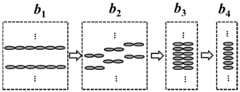
如图6所示,本发明提供一种叠阵半导体激光器窄线宽光谱合束装置的立体示意图,具体包括:叠阵半导体激光器1、快轴准直镜2、慢轴准直镜3、斜方棱镜组合4、柱面传输透镜5、衍射光栅6以及输出耦合镜7;沿叠阵半导体激光器1的光轴依次设置快轴准直镜2、慢轴准直镜3、斜方棱镜组合4、柱面传输透镜5和衍射光栅6,输出耦合镜7放置在衍射光栅6的-1级衍射光输出方向,并与-1级衍射光垂直;光谱合束方向为慢轴方向,沿水平方向(x轴)。As shown in Figure 6, the present invention provides a perspective schematic diagram of a narrow-linewidth spectral beam combining device for stacked semiconductor lasers, which specifically includes: stacked
本实施例中:In this example:
叠阵半导体激光器1的前腔面镀增透膜,透过率≥99%;斜方棱镜4及柱面传输透镜5的通光面均镀增透膜,透过率≥99%。斜方棱镜组合4置于叠阵半导体激光器1与柱面传输透镜5之间,柱面传输透镜5距离叠阵半导体激光器1和衍射光栅6的距离均为一倍透镜焦距;衍射光栅6与光轴按Littrow角放置。输出耦合镜7将部分比例的-1级衍射光束反馈回原发光单元实现波长锁定,其余的-1级衍射光作为输出激光。The front cavity surface of the
区别于实施例1,由于叠阵半导体激光,1的快轴方向等距排列多个阵列,每个阵列之间有一定间距的非发光区域。利用斜方棱镜组合4对光束进行分割重排,来填充叠阵光源之间的非发光区域,在缩短光谱合束方向光束宽度获得窄线宽的同时可以保持光谱合束后快轴方向光束质量基本不变。Different from
如图7所示,图中,b1为叠阵半导体激光器1出射的光斑图,b2为经过第一组斜方棱镜分割后的光斑,b3为经过第二组斜方棱镜分割后的光斑,b4为光谱合束输出的光斑图。As shown in Figure 7, in the figure, b1 is the light spot pattern emitted by the stacked
本发明的优点为:The advantages of the present invention are:
本发明的外腔光谱合束装置通过在外腔中引入斜方棱镜组合,对阵列半导体激光器出射的光束进行分割重排,将光谱合束方向的光束宽度缩短2/3左右,进而有效的将光谱合束线宽压缩2/3左右,使得该整体结构在小体积、高稳定度的情况下实现窄线宽的光谱合束输出。The external cavity spectral beam combining device of the present invention introduces a combination of rhombic prisms into the external cavity, splits and rearranges the beams emitted by the array semiconductor lasers, shortens the beam width in the spectral beam combining direction by about 2/3, and effectively converts the spectral The beam combining line width is compressed by about 2/3, so that the overall structure can achieve narrow line width spectral beam combining output in the case of small volume and high stability.
以上仅为本发明的优选实施例而已,并不用于限制本发明,对于本领域的技术人员来说,本发明可以有各种更改和变化。凡在本发明的精神和原则之内,所作的任何修改、等同替换、改进等,均应包含在本发明的保护范围之内。The above are only preferred embodiments of the present invention, and are not intended to limit the present invention. For those skilled in the art, the present invention may have various modifications and changes. Any modifications, equivalent replacements, improvements, etc. made within the spirit and principles of the present invention shall be included within the protection scope of the present invention.
Claims (10)
Translated fromChinesePriority Applications (1)
| Application Number | Priority Date | Filing Date | Title |
|---|---|---|---|
| CN202310216585.XACN116435872B (en) | 2023-03-08 | 2023-03-08 | Narrow linewidth spectrum beam combining device of array semiconductor laser |
Applications Claiming Priority (1)
| Application Number | Priority Date | Filing Date | Title |
|---|---|---|---|
| CN202310216585.XACN116435872B (en) | 2023-03-08 | 2023-03-08 | Narrow linewidth spectrum beam combining device of array semiconductor laser |
Publications (2)
| Publication Number | Publication Date |
|---|---|
| CN116435872Atrue CN116435872A (en) | 2023-07-14 |
| CN116435872B CN116435872B (en) | 2025-09-09 |
Family
ID=87091566
Family Applications (1)
| Application Number | Title | Priority Date | Filing Date |
|---|---|---|---|
| CN202310216585.XAActiveCN116435872B (en) | 2023-03-08 | 2023-03-08 | Narrow linewidth spectrum beam combining device of array semiconductor laser |
Country Status (1)
| Country | Link |
|---|---|
| CN (1) | CN116435872B (en) |
Cited By (2)
| Publication number | Priority date | Publication date | Assignee | Title |
|---|---|---|---|---|
| CN118249199A (en)* | 2024-05-07 | 2024-06-25 | 武汉锐科光纤激光技术股份有限公司 | External cavity tunable semiconductor laser |
| WO2025189570A1 (en)* | 2024-03-13 | 2025-09-18 | 武汉锐科光纤激光技术股份有限公司 | Semiconductor laser and laser device |
Citations (9)
| Publication number | Priority date | Publication date | Assignee | Title |
|---|---|---|---|---|
| US20110222574A1 (en)* | 2010-03-09 | 2011-09-15 | Massachusetts Institute Of Technology | Two-dimensional wavelength-beam-combining of lasers using first-order grating stack |
| CN202548385U (en)* | 2011-12-02 | 2012-11-21 | 北京工业大学 | Optical fiber coupling module of platform-type turning and reflecting single-tube semiconductor laser |
| US20130201560A1 (en)* | 2012-02-07 | 2013-08-08 | Robert H. Dueck | Two-dimensional Laser System Employing Two Dispersive Elements |
| US20150364900A1 (en)* | 2014-06-14 | 2015-12-17 | Bien Chann | Stabilization of wavelength beam combining laser systems in the non-wavelength beam combining direction |
| CN105428996A (en)* | 2015-12-09 | 2016-03-23 | 中国科学院长春光学精密机械与物理研究所 | Multi-grating structure-based semiconductor laser beam combination device and beam combination method |
| US20180019576A1 (en)* | 2016-07-14 | 2018-01-18 | BWT Beijing Ltd. | Laser beam combination apparatus |
| CN108429129A (en)* | 2018-05-08 | 2018-08-21 | 中国科学院半导体研究所 | The conjunction beam system and method for multi-thread array semiconductor laser grating external-cavity spectrum |
| US20210255467A1 (en)* | 2020-02-19 | 2021-08-19 | Fujian haichuang photoelectric co ltd | Semiconductor laser shaping device |
| CN115173219A (en)* | 2022-08-15 | 2022-10-11 | 北京工业大学 | High-brightness semiconductor laser module |
- 2023
- 2023-03-08CNCN202310216585.XApatent/CN116435872B/enactiveActive
Patent Citations (9)
| Publication number | Priority date | Publication date | Assignee | Title |
|---|---|---|---|---|
| US20110222574A1 (en)* | 2010-03-09 | 2011-09-15 | Massachusetts Institute Of Technology | Two-dimensional wavelength-beam-combining of lasers using first-order grating stack |
| CN202548385U (en)* | 2011-12-02 | 2012-11-21 | 北京工业大学 | Optical fiber coupling module of platform-type turning and reflecting single-tube semiconductor laser |
| US20130201560A1 (en)* | 2012-02-07 | 2013-08-08 | Robert H. Dueck | Two-dimensional Laser System Employing Two Dispersive Elements |
| US20150364900A1 (en)* | 2014-06-14 | 2015-12-17 | Bien Chann | Stabilization of wavelength beam combining laser systems in the non-wavelength beam combining direction |
| CN105428996A (en)* | 2015-12-09 | 2016-03-23 | 中国科学院长春光学精密机械与物理研究所 | Multi-grating structure-based semiconductor laser beam combination device and beam combination method |
| US20180019576A1 (en)* | 2016-07-14 | 2018-01-18 | BWT Beijing Ltd. | Laser beam combination apparatus |
| CN108429129A (en)* | 2018-05-08 | 2018-08-21 | 中国科学院半导体研究所 | The conjunction beam system and method for multi-thread array semiconductor laser grating external-cavity spectrum |
| US20210255467A1 (en)* | 2020-02-19 | 2021-08-19 | Fujian haichuang photoelectric co ltd | Semiconductor laser shaping device |
| CN115173219A (en)* | 2022-08-15 | 2022-10-11 | 北京工业大学 | High-brightness semiconductor laser module |
Non-Patent Citations (3)
| Title |
|---|
| ZHANG JUN: "Spectral beam combining of diode lasers extended into the non-SBC direction", OPTICS EXPRESS., 12 September 2022 (2022-09-12)* |
| 吴肖杰: "半导体激光光栅外腔光谱合束压窄光谱的理论研究", 强激光与粒子束, 30 September 2017 (2017-09-30)* |
| 彭航宇;张俊;付喜宏;曹军胜;王彪;: "高效外腔光谱合束半导体激光器阵列", 中国激光, no. 07, 10 July 2013 (2013-07-10)* |
Cited By (2)
| Publication number | Priority date | Publication date | Assignee | Title |
|---|---|---|---|---|
| WO2025189570A1 (en)* | 2024-03-13 | 2025-09-18 | 武汉锐科光纤激光技术股份有限公司 | Semiconductor laser and laser device |
| CN118249199A (en)* | 2024-05-07 | 2024-06-25 | 武汉锐科光纤激光技术股份有限公司 | External cavity tunable semiconductor laser |
Also Published As
| Publication number | Publication date |
|---|---|
| CN116435872B (en) | 2025-09-09 |
Similar Documents
| Publication | Publication Date | Title |
|---|---|---|
| US9093822B1 (en) | Multi-band co-bore-sighted scalable output power laser system | |
| US8824049B2 (en) | Scalable wavelength beam combining system and method | |
| US8767790B2 (en) | System and method for generating intense laser light from laser diode arrays | |
| CN106684702B (en) | It is a kind of to realize that lasing spectrum of semiconductor lasers closes the device of beam using double grating | |
| CN102986097B (en) | Selectivity is reorientated and is rotated wavelength beam combination system and method | |
| US7668214B2 (en) | Light source | |
| CN107272214A (en) | The spectrum beam combination device of the spectrum width of diffraction compression twice is realized using grating and reflecting element | |
| CN116435872A (en) | A Narrow Linewidth Spectral Beam Combining Device for Arrayed Semiconductor Lasers | |
| CN214044331U (en) | A blue light multi-single tube parallel double grating external cavity feedback beam combining device | |
| CN107946898A (en) | A kind of semiconductor laser beam merging apparatus and conjunction Shu Fangfa | |
| WO2017197883A1 (en) | Laser array beam combining device | |
| US20040174604A1 (en) | Laser diode bar integrator/reimager | |
| CN110676691B (en) | Semiconductor laser spectral beam combining device and method based on collimating-deflecting element | |
| CN110109259A (en) | The beam merging apparatus of semiconductor laser high light beam quality high-power output | |
| CN113206436B (en) | Multilayer blue light semiconductor laser spectrum beam combining device | |
| CN108429129A (en) | The conjunction beam system and method for multi-thread array semiconductor laser grating external-cavity spectrum | |
| CN104678557A (en) | Stabilization of high-power wavelength beam combining system | |
| CN112531462B (en) | Bragg grating external cavity semiconductor laser module beam combining device | |
| CN209946540U (en) | Semiconductor laser beam combining device with high beam quality and high power output | |
| CN112563879A (en) | Dense wavelength beam combining device of multi-single-tube semiconductor laser | |
| CN116706689A (en) | Distributed multi-single-tube semiconductor laser beam combining device | |
| CN115967014A (en) | A Spectrum Combining Device for Linear Array Semiconductor Lasers | |
| CN115714303A (en) | High-power optical fiber coupling system based on polarization plane multiplexing | |
| CN204103247U (en) | A kind of miniaturized compact spectrum beam combination semicondcutor laser unit | |
| CN108803065B (en) | Dense optical fiber array spectrum beam combining device and method |
Legal Events
| Date | Code | Title | Description |
|---|---|---|---|
| PB01 | Publication | ||
| PB01 | Publication | ||
| SE01 | Entry into force of request for substantive examination | ||
| SE01 | Entry into force of request for substantive examination | ||
| GR01 | Patent grant | ||
| GR01 | Patent grant |