CN116434805A - Three-dimensional memory device, memory system including the same, and method of programming the same - Google Patents
Three-dimensional memory device, memory system including the same, and method of programming the sameDownload PDFInfo
- Publication number
- CN116434805A CN116434805ACN202310417300.9ACN202310417300ACN116434805ACN 116434805 ACN116434805 ACN 116434805ACN 202310417300 ACN202310417300 ACN 202310417300ACN 116434805 ACN116434805 ACN 116434805A
- Authority
- CN
- China
- Prior art keywords
- unselected
- memory
- voltage
- pass voltage
- pass
- Prior art date
- Legal status (The legal status is an assumption and is not a legal conclusion. Google has not performed a legal analysis and makes no representation as to the accuracy of the status listed.)
- Pending
Links
Images


Classifications
- G—PHYSICS
- G11—INFORMATION STORAGE
- G11C—STATIC STORES
- G11C16/00—Erasable programmable read-only memories
- G11C16/02—Erasable programmable read-only memories electrically programmable
- G11C16/06—Auxiliary circuits, e.g. for writing into memory
- G11C16/10—Programming or data input circuits
- G11C16/102—External programming circuits, e.g. EPROM programmers; In-circuit programming or reprogramming; EPROM emulators
- G—PHYSICS
- G11—INFORMATION STORAGE
- G11C—STATIC STORES
- G11C16/00—Erasable programmable read-only memories
- G11C16/02—Erasable programmable read-only memories electrically programmable
- G11C16/06—Auxiliary circuits, e.g. for writing into memory
- G11C16/10—Programming or data input circuits
- G—PHYSICS
- G11—INFORMATION STORAGE
- G11C—STATIC STORES
- G11C16/00—Erasable programmable read-only memories
- G11C16/02—Erasable programmable read-only memories electrically programmable
- G11C16/06—Auxiliary circuits, e.g. for writing into memory
- G11C16/08—Address circuits; Decoders; Word-line control circuits
- G—PHYSICS
- G11—INFORMATION STORAGE
- G11C—STATIC STORES
- G11C16/00—Erasable programmable read-only memories
- G11C16/02—Erasable programmable read-only memories electrically programmable
- G11C16/06—Auxiliary circuits, e.g. for writing into memory
- G11C16/10—Programming or data input circuits
- G11C16/12—Programming voltage switching circuits
- G—PHYSICS
- G11—INFORMATION STORAGE
- G11C—STATIC STORES
- G11C16/00—Erasable programmable read-only memories
- G11C16/02—Erasable programmable read-only memories electrically programmable
- G11C16/06—Auxiliary circuits, e.g. for writing into memory
- G11C16/10—Programming or data input circuits
- G11C16/14—Circuits for erasing electrically, e.g. erase voltage switching circuits
- G—PHYSICS
- G11—INFORMATION STORAGE
- G11C—STATIC STORES
- G11C16/00—Erasable programmable read-only memories
- G11C16/02—Erasable programmable read-only memories electrically programmable
- G11C16/06—Auxiliary circuits, e.g. for writing into memory
- G11C16/24—Bit-line control circuits
- G—PHYSICS
- G11—INFORMATION STORAGE
- G11C—STATIC STORES
- G11C16/00—Erasable programmable read-only memories
- G11C16/02—Erasable programmable read-only memories electrically programmable
- G11C16/06—Auxiliary circuits, e.g. for writing into memory
- G11C16/26—Sensing or reading circuits; Data output circuits
- G—PHYSICS
- G11—INFORMATION STORAGE
- G11C—STATIC STORES
- G11C16/00—Erasable programmable read-only memories
- G11C16/02—Erasable programmable read-only memories electrically programmable
- G11C16/06—Auxiliary circuits, e.g. for writing into memory
- G11C16/34—Determination of programming status, e.g. threshold voltage, overprogramming or underprogramming, retention
- G11C16/3404—Convergence or correction of memory cell threshold voltages; Repair or recovery of overerased or overprogrammed cells
- G—PHYSICS
- G11—INFORMATION STORAGE
- G11C—STATIC STORES
- G11C16/00—Erasable programmable read-only memories
- G11C16/02—Erasable programmable read-only memories electrically programmable
- G11C16/06—Auxiliary circuits, e.g. for writing into memory
- G11C16/34—Determination of programming status, e.g. threshold voltage, overprogramming or underprogramming, retention
- G11C16/3418—Disturbance prevention or evaluation; Refreshing of disturbed memory data
- G11C16/3427—Circuits or methods to prevent or reduce disturbance of the state of a memory cell when neighbouring cells are read or written
- G—PHYSICS
- G11—INFORMATION STORAGE
- G11C—STATIC STORES
- G11C16/00—Erasable programmable read-only memories
- G11C16/02—Erasable programmable read-only memories electrically programmable
- G11C16/04—Erasable programmable read-only memories electrically programmable using variable threshold transistors, e.g. FAMOS
- G11C16/0483—Erasable programmable read-only memories electrically programmable using variable threshold transistors, e.g. FAMOS comprising cells having several storage transistors connected in series
Landscapes
- Read Only Memory (AREA)
- Non-Volatile Memory (AREA)
- Semiconductor Memories (AREA)
Abstract
Translated fromChinese
Description
Translated fromChinese本公开是申请日为2021年04月01日,申请号为202180001136.2,发明名称为“三维存储设备、包括其的存储系统及对其进行编程的方法”的专利申请的分案申请。This disclosure is a divisional application of a patent application with an application date of April 1, 2021, an application number of 202180001136.2, and an invention titled "Three-dimensional storage device, a storage system including it, and a method for programming it".
技术领域technical field
本公开内容总体上涉及半导体技术领域,具体而言,涉及编程三维(3D)存储器的方法。The present disclosure relates generally to the field of semiconductor technology and, in particular, to methods of programming three-dimensional (3D) memories.
背景技术Background technique
随着存储设备缩小到较小的管芯尺寸以降低制造成本并增加存储密度,由于工艺技术的局限性和可靠性问题,平面存储单元的缩放面临挑战。三维(3D)存储器架构可以解决平面存储单元中的密度和性能限制。As memory devices shrink to smaller die sizes to reduce manufacturing costs and increase storage density, scaling of planar memory cells is challenging due to process technology limitations and reliability issues. Three-dimensional (3D) memory architectures can address density and performance limitations in planar memory cells.
在3D NAND闪存存储器中,多层存储单元可以垂直堆叠,使得每单位面积的存储密度可以大大增加。垂直堆叠的存储单元可形成存储串,其中存储单元的沟道在每个存储串中连接。在操作期间,可以同时编程和读取共享相同字线的存储页中的存储单元。然而,并非将同一存储页中的所有存储单元都选择编程到同一逻辑状态。那些未选存储单元可遭受编程干扰。类似地,同一存储串中的未选存储单元可能遭受通过干扰(pass disturb)。因此,需要一种抑制编程干扰和通过干扰两者以改进3D NAND存储器的性能和可靠性的方法。In 3D NAND flash memory, multiple layers of memory cells can be stacked vertically, so that the storage density per unit area can be greatly increased. Vertically stacked memory cells may form strings, where the channels of the memory cells are connected in each string. During operation, memory cells in memory pages sharing the same word line can be programmed and read simultaneously. However, not all memory cells in the same memory page are selected for programming to the same logic state. Those unselected memory cells can suffer program disturb. Similarly, unselected memory cells in the same string may suffer from pass disturbance. Therefore, there is a need for a method of both suppressing program disturb and via disturb to improve the performance and reliability of 3D NAND memory.
发明内容Contents of the invention
本公开内容描述了用于三维(3D)存储设备的编程方法和电路的实施例。This disclosure describes embodiments of programming methods and circuits for three-dimensional (3D) memory devices.
本公开内容的一方面提供了一种用于对三维(3D)存储设备进行编程的方法。3D存储设备具有多个存储串,多个存储串具有垂直堆叠的存储单元,且每个存储单元可通过字线和位线寻址。对3D存储设备进行编程的方法包括以下步骤:在所选字线上施加编程电压;在第一组未选字线上施加第一通过电压;以及在第二组未选字线上施加第二通过电压,其中,第二通过电压不同于第一通过电压。An aspect of the present disclosure provides a method for programming a three-dimensional (3D) memory device. A 3D memory device has a plurality of memory strings with vertically stacked memory cells, and each memory cell is addressable through a word line and a bit line. The method for programming a 3D memory device comprises the steps of: applying a programming voltage on a selected word line; applying a first pass voltage on a first group of unselected word lines; and applying a second pass voltage on a second group of unselected word lines. A pass voltage, wherein the second pass voltage is different from the first pass voltage.
在一些实施例中,该方法还包括确定用于连接到第一组未选字线的第一未选存储单元集合的第一最大通过电压,以抑制第一未选存储单元集合上的通过干扰;以及确定用于连接到第二组未选字线的第二未选存储单元集合的第二最大通过电压,以抑制第二未选存储单元集合上的通过干扰。In some embodiments, the method further includes determining a first maximum pass voltage for a first set of unselected memory cells connected to a first set of unselected word lines to suppress pass disturb on the first set of unselected memory cells and determining a second maximum pass voltage for a second set of unselected memory cells connected to a second set of unselected word lines to suppress pass disturb on the second set of unselected memory cells.
在一些实施例中,确定第一最大通过电压包括测量第一未选存储单元集合的阈值电压的偏移;以及当第一未选存储单元集合的阈值电压的偏移小于最大允许偏移时,将第一最大通过电压设置为第一通过电压。In some embodiments, determining the first maximum pass voltage includes measuring a shift in threshold voltage of the first set of unselected memory cells; and when the shift in threshold voltage of the first set of unselected memory cells is less than the maximum allowable shift, The first maximum pass voltage is set as the first pass voltage.
在一些实施例中,方法还包括当第一未选存储单元集合的阈值电压的偏移大于最大允许偏移时,将第一通过电压减小预定值。In some embodiments, the method further includes reducing the first pass voltage by a predetermined value when the threshold voltages of the first set of unselected memory cells are offset by more than a maximum allowable offset.
在一些实施例中,测量第一未选存储单元集合的阈值电压的偏移包括测量处于擦除状态的第一未选存储单元集合的阈值电压。In some embodiments, measuring the shift in the threshold voltage of the first set of unselected memory cells includes measuring the threshold voltage of the first set of unselected memory cells in an erased state.
在一些实施例中,确定第二最大通过电压包括测量第二未选存储单元集合的阈值电压的偏移;以及当第二未选存储单元集合的阈值电压的偏移小于最大允许偏移时,将第二最大通过电压设置为第二通过电压。In some embodiments, determining the second maximum pass voltage includes measuring a shift in threshold voltage of the second set of unselected memory cells; and when the shift in threshold voltage of the second set of unselected memory cells is less than the maximum allowable shift, The second maximum pass voltage is set as the second pass voltage.
在一些实施例中,方法还包括当第二未选存储单元集合的阈值电压的偏移大于最大允许偏移时,将第二通过电压减小预定值。In some embodiments, the method further includes reducing the second pass voltage by a predetermined value when the threshold voltages of the second set of unselected memory cells are offset by more than a maximum allowable offset.
在一些实施例中,测量第二未选存储单元集合的阈值电压的偏移包括测量处于擦除状态的第二未选存储单元集合的阈值电压。In some embodiments, measuring the shift in the threshold voltage of the second set of unselected memory cells includes measuring the threshold voltage of the second set of unselected memory cells in an erased state.
在一些实施例中,施加第一通过电压和施加第二通过电压包括初始地施加具有预先给定值的电压以抑制第四未选存储单元集合上的编程干扰,其中,第四未选存储单元集合连接到所选字线。In some embodiments, applying the first pass voltage and applying the second pass voltage includes initially applying a voltage having a predetermined value to suppress program disturb on a fourth set of unselected memory cells, wherein the fourth unselected memory cells set is connected to the selected word line.
在一些实施例中,方法还包括当第四未选存储单元集合的阈值电压的偏移小于最大允许偏移时,确定具有预先给定值的电压。In some embodiments, the method further includes determining a voltage having a predetermined value when the deviation of the threshold voltage of the fourth unselected memory cell set is smaller than a maximum allowable deviation.
在一些实施例中,该方法还包括将所选位线连接到地以对连接到所选位线和所选字线的所选存储单元进行编程;以及在未选位线上施加禁止电压,以禁止对连接到未选位线的未选存储单元进行编程。In some embodiments, the method further includes connecting the selected bit line to ground to program the selected memory cells connected to the selected bit line and the selected word line; and applying an inhibit voltage on the unselected bit lines, to inhibit programming of unselected memory cells connected to unselected bit lines.
在一些实施例中,施加编程电压包括施加在约10V与20V之间的范围内的电压。In some embodiments, applying the programming voltage includes applying a voltage in a range between about 10V and 20V.
在一些实施例中,施加第一通过电压和施加第二通过电压包括施加在约6V到约13V之间的范围内的电压。In some embodiments, applying the first pass voltage and applying the second pass voltage includes applying a voltage in a range between about 6V and about 13V.
本公开内容的另一方面提供了一种三维(3D)存储设备。该3D存储设备包括多个存储单元,连接到被配置用于寻址多个存储单元中的每一个存储单元的字线和位线,其中,多个存储单元被垂直堆叠。3D存储设备还包括外围电路,被配置为对所选存储单元进行编程。外围电路包括控制电路,被配置为将控制信号发送到字线驱动器。字线驱动器根据控制信号被配置为在所选字线上施加编程电压;在第一组未选字线上施加第一通过电压;以及在第二组未选字线上施加第二通过电压,其中,第二通过电压不同于第一通过电压。Another aspect of the present disclosure provides a three-dimensional (3D) storage device. The 3D memory device includes a plurality of memory cells connected to word lines and bit lines configured to address each of the plurality of memory cells, wherein the plurality of memory cells are vertically stacked. The 3D memory device also includes peripheral circuitry configured to program selected memory cells. The peripheral circuit includes a control circuit configured to send a control signal to the word line driver. The word line driver is configured according to the control signal to apply a programming voltage on the selected word line; apply a first pass voltage on the first group of unselected word lines; and apply a second pass voltage on the second group of unselected word lines, Wherein, the second pass voltage is different from the first pass voltage.
在一些实施例中,外围电路还被配置为将所选位线连接到地以对由所选字线和所选位线寻址的所选存储单元进行编程;以及在未选位线上施加禁止电压,以禁止对由未选位线寻址的未选存储单元进行编程。In some embodiments, the peripheral circuit is further configured to connect the selected bit line to ground to program the selected memory cells addressed by the selected word line and the selected bit line; and apply Inhibit voltage to inhibit programming of unselected memory cells addressed by unselected bit lines.
在一些实施例中,外围电路还被配置为确定第一最大通过电压,以抑制连接到第一组未选字线的第一未选存储单元集合上的通过干扰;以及确定第二最大通过电压以抑制连接到第二组未选字线的第二未选存储单元集合上的通过干扰。In some embodiments, the peripheral circuit is further configured to determine a first maximum pass voltage to suppress pass disturbances on a first set of unselected memory cells connected to a first set of unselected word lines; and determine a second maximum pass voltage to suppress the pass disturb on the second set of unselected memory cells connected to the second set of unselected word lines.
在一些实施例中,当第一未选存储单元集合的阈值电压的偏移小于最大允许偏移时,确定第一最大通过电压。In some embodiments, the first maximum pass voltage is determined when the threshold voltages of the first set of unselected memory cells are shifted by less than a maximum allowable shift.
在一些实施例中,当第二未选存储单元集合的阈值电压的偏移小于最大允许偏移时,确定第二最大通过电压。In some embodiments, the second maximum pass voltage is determined when the threshold voltages of the second set of unselected memory cells are shifted by less than a maximum allowable shift.
在一些实施例中,第一未选存储单元集合和第二未选存储单元集合处于擦除状态。In some embodiments, the first set of unselected memory cells and the second set of unselected memory cells are in an erased state.
在一些实施例中,当分别在第一组未选字线和第二组所选字线上施加第一最大通过电压和第二最大通过电压时,连接到所选字线的第四未选存储单元集合的阈值电压的偏移小于最大允许偏移。In some embodiments, when the first maximum pass voltage and the second maximum pass voltage are applied to the first set of unselected word lines and the second set of selected word lines, respectively, the fourth unselected The threshold voltages of the set of memory cells are shifted less than the maximum allowable shift.
本公开内容还提供了一种存储系统,其中,存储系统包括存储器控制器和三维存储设备。存储器芯片包括连接到字线和位线的多个存储单元,字线和位线被配置用于寻址多个存储单元中的每一个,其中,多个存储单元被垂直堆叠。存储器芯片还包括外围电路,被配置为对所选存储单元进行编程,外围电路包括控制电路。控制电路被配置为将控制信号发送到字线驱动器,其中,字线驱动器根据控制信号被配置为在所选字线上施加编程电压;在第一组未选字线上施加第一通过电压;以及在第二组未选字线上施加第二通过电压,其中,第二通过电压不同于第一通过电压。The present disclosure also provides a storage system, wherein the storage system includes a memory controller and a three-dimensional storage device. The memory chip includes a plurality of memory cells connected to word lines and bit lines configured to address each of the plurality of memory cells, wherein the plurality of memory cells are vertically stacked. The memory chip also includes peripheral circuitry configured to program the selected memory cells, the peripheral circuitry including control circuitry. The control circuit is configured to send a control signal to the word line driver, wherein the word line driver is configured to apply a programming voltage on the selected word line according to the control signal; apply a first pass voltage on the first group of unselected word lines; And applying a second pass voltage on the second group of unselected word lines, wherein the second pass voltage is different from the first pass voltage.
根据本公开内容的说明书、权利要求书和附图,本领域技术人员可以理解本公开内容的其他方面。Other aspects of the present disclosure can be understood by those skilled in the art from the specification, claims and drawings of the present disclosure.
附图说明Description of drawings
并入本文并形成说明书的一部分的附图示出了本公开内容的实施例,并且与说明书一起进一步用于解释本公开内容的原理并且使得相关领域技术人员能够实施和使用本公开内容。The accompanying drawings, which are incorporated in and form a part of this specification, illustrate embodiments of the disclosure and, together with the description, further serve to explain the principles of the disclosure and to enable those skilled in the relevant art to make and use the disclosure.
图1示出了根据本公开内容的一些实施例的示例性三维(3D)存储器管芯的示意性俯视图。Figure 1 shows a schematic top view of an exemplary three-dimensional (3D) memory die, according to some embodiments of the present disclosure.
图2示出了根据本公开内容的一些实施例的3D存储器管芯的区域的示意性俯视图。Figure 2 shows a schematic top view of a region of a 3D memory die according to some embodiments of the present disclosure.
图3示出了根据本公开内容的一些实施例的示例性3D存储阵列结构的一部分的透视图。Figure 3 illustrates a perspective view of a portion of an exemplary 3D memory array structure according to some embodiments of the present disclosure.
图4示出了根据本公开内容的一些实施例的3D存储设备的截面图。FIG. 4 shows a cross-sectional view of a 3D memory device according to some embodiments of the present disclosure.
图5-6示出了根据本公开内容的一些实施例的3D存储设备的示意性电路图。5-6 show schematic circuit diagrams of 3D storage devices according to some embodiments of the present disclosure.
图7A示出了根据本公开内容的一些实施例的在施加具有通过电压的脉冲之后各种字线组中的存储单元的阈值电压偏移。7A illustrates threshold voltage shifts of memory cells in various word line groups after application of pulses with pass voltages, according to some embodiments of the present disclosure.
图7B示出了根据本公开内容的一些实施例的在施加具有各种通过电压的脉冲之后特定字线组中的存储单元的阈值电压偏移。7B illustrates threshold voltage shifts of memory cells in a particular word line group after application of pulses with various pass voltages, according to some embodiments of the present disclosure.
图8示出了根据本公开内容的一些实施例的确定特定字线组中的存储单元的最大通过电压的操作流程。FIG. 8 illustrates an operation flow for determining a maximum pass voltage of memory cells in a particular word line group according to some embodiments of the present disclosure.
图9A-C示出了根据本公开内容的一些实施例的具有一个或多个存储器芯片的存储系统。9A-C illustrate a memory system with one or more memory chips, according to some embodiments of the present disclosure.
图10示出了根据本公开内容的一些实施例的存储器管芯的示意图。Figure 10 shows a schematic diagram of a memory die according to some embodiments of the disclosure.
结合附图,依据下面阐述的具体实施方式,本发明的特征和优点将变得更加明显,在附图中,相似的附图标记始终标识相应的元件。在附图中,相似的附图标记通常表示相同、功能相似和/或结构相似的元件。元件首次出现的图由相应附图标记中最左边的数字指示。The features and advantages of the present invention will become more apparent from the detailed description set forth below when taken in conjunction with the accompanying drawings, in which like reference numerals identify corresponding elements throughout. In the drawings, like reference numbers generally indicate identical, functionally similar, and/or structurally similar elements. The drawing in which an element first appears is indicated by the leftmost digit(s) in the corresponding reference number.
将参考附图描述本公开内容的实施例。Embodiments of the present disclosure will be described with reference to the drawings.
具体实施方式Detailed ways
尽管讨论了具体的配置和布置,但应该理解,这仅仅是为了说明的目的而进行的。相关领域的技术人员将认识到,在不脱离本公开内容的精神和范围的情况下,可以使用其他配置和布置。对于相关领域的技术人员显而易见的是,本公开内容还可以用于各种其他应用中。While specific configurations and arrangements are discussed, it should be understood that this is done for illustration purposes only. A person skilled in the relevant art will recognize that other configurations and arrangements may be used without departing from the spirit and scope of the present disclosure. It will be apparent to those skilled in the relevant art that the present disclosure may also be used in various other applications.
应注意到,在说明书中对“一个实施例”、“实施例”、“示例性实施例”、“一些实施例”等的引用指示所描述的实施例可以包括特定的特征、结构或特性,但是每个实施例可能不一定包括该特定的特征、结构或特性。而且,这样的短语不一定指代相同的实施例。此外,当结合实施例描述特定特征、结构或特性时,无论是否明确描述,结合其他实施例来影响这样的特征、结构或特性都在相关领域的技术人员的知识范围内。It should be noted that references in the specification to "one embodiment," "an embodiment," "exemplary embodiment," "some embodiments," etc. indicate that the described embodiments may include a particular feature, structure, or characteristic, But each embodiment may not necessarily include that particular feature, structure or characteristic. Moreover, such phrases are not necessarily referring to the same embodiment. Furthermore, when a particular feature, structure or characteristic is described in conjunction with an embodiment, whether or not explicitly described, it is within the purview of those skilled in the relevant art to effect such feature, structure or characteristic in conjunction with other embodiments.
通常,可以至少部分地从上下文中的用法理解术语。例如,如本文所用的术语“一个或多个”至少部分取决于上下文,可用于以单数意义描述任何特征、结构或特性,或可用于以复数意义描述特征、结构或特性的组合。类似地,至少部分取决于上下文,诸如“一”、“一个”或“该”的术语同样可以被理解为表达单数用法或表达复数用法。另外,术语“基于”可以被理解为不一定旨在传达排他性的因素集合,而是可以允许存在不一定明确描述的其他因素,这同样至少部分地取决于上下文。In general, a term can be understood, at least in part, from its usage in context. For example, the term "one or more" as used herein may be used in the singular to describe any feature, structure or characteristic, or may be used in the plural to describe a combination of features, structures or characteristics, depending at least in part on the context. Similarly, terms such as "a", "an" or "the" may equally be read to express singular usage or to express plural usage, depending at least in part on the context. Additionally, the term "based on" may be understood as not necessarily intended to convey an exclusive set of factors, but may allow for the presence of other factors not necessarily explicitly described, again depending at least in part on context.
应当容易理解的是,本公开内容中的“在……上”、“在……之上”和“在……上方”的含义应以最宽泛的方式来解释,使得“在……上”不仅意味着“直接在某物上”,而且还包括其间具有中间特征或层的“在某物上”的含义。此外,“在……之上”或“在……上方”不仅意味着“在某物之上”或“在某物上方”,而且还可以包括其间没有中间特征或层的“在某物之上”或“在某物上方”的含义(即,直接在某物上)。It should be readily understood that the meanings of "on", "over" and "above" in this disclosure are to be interpreted in the broadest manner such that "on" Not only does it mean "directly on something", but it also includes the meaning of "on something" with intermediate features or layers in between. Furthermore, "on" or "above" not only means "on something" or "above something" but can also include "beyond something" without intermediate features or layers in between. on" or "over something" (i.e., directly on something).
此外,为了便于描述,可以在本文使用诸如“在……之下”、“在……下方”、“下”、“在……之上”、“上”等的空间相对术语来描述如图所示的一个元件或特征与另一个元件或特征的关系。除了附图中所示的取向之外,空间相对术语旨在涵盖设备在使用或处理步骤中的不同取向。该装置可以以其他方式定向(旋转90度或在其他取向)并且同样可以相应地解释本文使用的空间相关描述词。In addition, for the convenience of description, spatially relative terms such as "below", "below", "below", "above", "on" etc. may be used herein to describe The relationship of one element or feature to another element or feature is shown. Spatially relative terms are intended to encompass different orientations of the device in use or handling steps in addition to the orientation depicted in the figures. The device may be otherwise oriented (rotated 90 degrees or at other orientations) and the spatially relative descriptors used herein interpreted accordingly.
如本文所使用的,术语“衬底”是指在其上添加后续材料层的材料。衬底包括“顶”表面和“底”表面。衬底的顶表面通常是形成半导体器件的位置,因此,除非另外说明,否则半导体器件形成在衬底的顶侧。底表面与顶表面相对,因此衬底的底侧与衬底的顶侧相对。衬底本身可以被图案化。添加在衬底顶部的材料可以被图案化或可以保持未图案化。此外,衬底可以包括多种半导体材料,例如硅,锗、砷化镓、磷化铟等。可替换地,衬底可以由非导电材料制成,例如玻璃、塑料或蓝宝石晶圆。As used herein, the term "substrate" refers to a material on which subsequent layers of material are added. The substrate includes a "top" surface and a "bottom" surface. The top surface of the substrate is typically where semiconductor devices are formed, and thus, unless otherwise stated, semiconductor devices are formed on the top side of the substrate. The bottom surface is opposite the top surface, so the bottom side of the substrate is opposite the top side of the substrate. The substrate itself can be patterned. Materials added on top of the substrate can be patterned or can remain unpatterned. In addition, the substrate may include various semiconductor materials, such as silicon, germanium, gallium arsenide, indium phosphide, and the like. Alternatively, the substrate can be made of a non-conductive material such as glass, plastic or a sapphire wafer.
如本文所使用的,术语“层”是指包括具有厚度的区域的材料部分。层具有顶侧和底侧,其中层的底侧相对靠近衬底,而顶侧相对远离衬底。层可以在整个下层或上层结构上延伸,或者可以具有小于下层或上层结构范围的范围。此外,层可以是厚度小于连续结构的厚度的均匀或不均匀连续结构的区域。例如,层可以位于连续结构的顶表面和底表面之间或在顶表面和底表面处的任何一组水平平面之间。层可以水平、垂直和/或沿着锥形表面延伸。衬底可以是层,其中可以包括一层或多层,和/或可以在其上、上方和/或其下具有一层或多层。层可以包括多个层。例如,互连层可以包括一个或多个导电层和触点层(其中形成有触点、互连线和/或垂直互连通路(VIA))以及一个或多个电介质层。As used herein, the term "layer" refers to a portion of material that includes regions having a thickness. The layer has a top side and a bottom side, wherein the bottom side of the layer is relatively close to the substrate and the top side is relatively far from the substrate. A layer may extend across the entire underlying or superstructure, or may have an extent that is less than the extent of the underlying or superstructure. Furthermore, a layer may be a region of a uniform or non-uniform continuous structure with a thickness less than that of the continuous structure. For example, a layer may be located between the top and bottom surfaces of the continuous structure or between any set of horizontal planes at the top and bottom surfaces. Layers may extend horizontally, vertically and/or along the tapered surface. A substrate can be a layer, can include one or more layers therein, and/or can have one or more layers thereon, above, and/or below. Layers may include multiple layers. For example, an interconnect layer may include one or more conductive and contact layers (in which contacts, interconnect lines, and/or vertical interconnect vias (VIAs) are formed) and one or more dielectric layers.
在本公开内容中,为了便于描述,“级”用于指代沿垂直方向具有基本相同高度的元件。例如,字线和下面的栅极电介质层可以被称为“一级”,字线和下面的绝缘层可以一起被称为“一级”,具有基本相同高度的字线可以是被称为“一级字线”或类似的等。In the present disclosure, for convenience of description, "stage" is used to refer to elements having substantially the same height in a vertical direction. For example, a word line and the underlying gate dielectric layer may be referred to as a "level one", a word line and an underlying insulating layer may be collectively referred to as a "level one", and word lines having substantially the same height may be referred to as a "level one".
如本文所使用的,术语“标称/标称地”是指在产品或过程的设计阶段期间设定的部件或过程步骤的特性或参数的期望值或目标值,以及高于和/或低于期望值的值的范围。值的范围可以是由于制造工艺或公差的轻微变化而引起的。如本文所使用的,术语“约”表示可以基于与主题半导体器件相关联的特定技术节点而变化的给定量的值。基于特定的技术节点,术语“约”可以表示给定量的值,该给定量例如在该值的10-30%内变化(例如,值的±10%、±20%或±30%)。As used herein, the term "nominal" refers to an expected or target value for a characteristic or parameter of a component or process step set during the design phase of a product or process, and above and/or below The range of values for the expected value. The range of values may be due to slight variations in manufacturing process or tolerances. As used herein, the term "about" indicates a value for a given quantity that may vary based on the particular technology node associated with the subject semiconductor device. The term "about" may refer to a value of a given quantity that varies, for example, within 10-30% of the value (eg, ±10%, ±20%, or ±30% of the value), based on the particular technology node.
在本公开内容中,术语“水平的/水平地/横向的/横向地”表示标称上平行于衬底的侧表面,术语“垂直的”或“垂直地”表示标称上垂直于衬底的侧表面。In this disclosure, the term "horizontal/horizontal/lateral/laterally" means nominally parallel to the side surface of the substrate, and the term "perpendicular" or "vertically" means nominally perpendicular to the substrate. side surface.
如本文所使用的,术语“3D存储器”是指在横向定向的衬底上具有垂直定向的存储单元晶体管串(在本文中称为“存储串”,诸如NAND串)的三维(3D)半导体器件,使得存储串相对于衬底在垂直方向上延伸。As used herein, the term "3D memory" refers to a three-dimensional (3D) semiconductor device having vertically oriented strings of memory cell transistors (referred to herein as "strings", such as NAND strings) on a laterally oriented substrate , so that the strings extend in a vertical direction relative to the substrate.
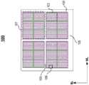
图1示出了根据本公开内容的一些实施例的示例性三维(3D)存储设备100的俯视图。3D存储设备100可以是存储器芯片(封装)、存储器管芯或存储器管芯的任何部分,并且可以包括一个或多个存储平面101,每个存储平面可以包括多个存储块103。可以在每个存储平面101上进行相同和并发的操作。大小可以是兆字节(MB)的存储块103是执行擦除操作的最小大小。如图1所示,示例性3D存储设备100包括四个存储平面101,并且每个存储平面101包括六个存储块103。每个存储块103可以包括多个存储单元,其中每个存储单元可以通过诸如位线和字线的互连来寻址。位线和字线可以垂直地布置(例如,分别在行和列中),从而形成金属线的阵列。在图1中,将位线和字线的方向标记为“BL”和“WL”。在本公开内容中,存储块103也被称为“存储阵列”或“阵列”。存储阵列是存储设备中的核心区域,执行储存功能。FIG. 1 illustrates a top view of an exemplary three-dimensional (3D)
3D存储设备100还包括外围区域105,围绕存储平面101的区域。外围区域105包含许多数字、模拟和/或混合信号电路以支持存储阵列的功能,例如,页缓冲器、行和列解码器以及读出放大器。外围电路使用有源和/或无源半导体器件,例如晶体管、二极管、电容器、电阻器等,这对于本领域普通技术人员来说是显而易见的。The
注意,图1所示的3D存储设备100中的存储平面101的布置和每个存储平面101中的存储块103的布置仅作为示例,并不限制本公开内容的范围。Note that the arrangement of the storage planes 101 in the
参考图2,示出了根据本公开内容的一些实施例的图1中的区域108的放大的俯视图。3D存储设备100的区域108可以包括阶梯区域210和沟道结构区域211。沟道结构区域211可以包括存储串212的阵列,每个存储串包括多个堆叠的存储单元。阶梯区域210可以包括阶梯结构和形成在阶梯结构上的触点结构214的阵列。在一些实施例中,在WL方向上跨沟道结构区域211和阶梯区域210延伸的多个狭缝结构216可以将存储块划分为多个存储指状物218。至少一些狭缝结构216可以用作沟道结构区域211中的存储串212的阵列的公共源极触点(例如,阵列公共源极)。例如,可以在每个存储指状物218的中间设置上选择栅极切口220以将存储指状物218的上选择栅极(TSG)划分为两个部分,从而可以将存储指状物划分为两个存储片224,其中共享相同字线的存储片224中的存储单元形成可编程(读/写)存储页。虽然可以在存储块级别执行3D NAND存储器的擦除操作,但可以在存储页级别执行读写操作。存储页的大小可以为千字节(KB)。在一些实施例中,区域108还包括虚设存储串222,用于制造期间的工艺变化控制和/或用于附加的机械支撑。Referring to FIG. 2 , an enlarged top view of
图3示出了根据本公开内容的一些实施例的示例性三维(3D)存储阵列结构300的一部分的透视图。存储阵列结构300包括衬底330,在衬底330上方的绝缘膜331,在绝缘膜331上方的一级下选择栅极(LSG)332以及多级控制栅极333,也称为“字线(WL)”,堆叠在LSG332的顶部上以形成由交替的导电层和电介质层组成的膜叠层335。为了清楚起见,在图3中未示出与各级控制栅极相邻的电介质层。FIG. 3 illustrates a perspective view of a portion of an exemplary three-dimensional (3D)
每一级的控制栅极被穿过膜叠层335的狭缝结构216-1和216-2隔开。存储阵列结构300还包括在控制栅极333的叠层上方的一级上选择栅极(TSG)334。TSG 334、控制栅极333和LSG 332的叠层也被称为“栅电极”。存储阵列结构300还包括在相邻的LSG 332之间的衬底330的部分中的存储串212和掺杂的源极线区域344。每个存储串212包括延伸穿过绝缘膜331及由交替的导电层和电介质层构成的膜叠层335的沟道孔336。存储串212还包括在沟道孔336的侧壁上的存储膜337,在存储膜337上方的沟道层338以及被沟道层338围绕的芯填充膜339。存储单元340(例如,340-1、340-2、340-3)可以形成在控制栅极333(例如,333-1、333-2、333-3)和存储串212的交点处。沟道层338的响应于相应控制栅极的部分也称为存储单元的沟道338。存储阵列结构300还包括在TSG 334上方与存储串212连接的多条位线(BL)341。存储阵列结构300还包括通过多个触点结构214与栅电极连接的多条金属互连线343。膜叠层335的边缘构造成阶梯形,以允许到每一级栅电极的电连接。The control gates of each stage are separated by slit structures 216 - 1 and 216 - 2 through the
在图3中,出于说明目的,示出了三级控制栅极333-1、333-2和333-3以及一级TSG334和一级LSG 332。在该示例中,每个存储串212可以包括分别对应于控制栅极333-1、333-2和333-3的三个存储单元340-1、340-2和340-3。在一些实施例中,控制栅极的数量和存储单元的数量可以大于三个以增加储存容量。存储阵列结构300还可以包括其他结构,例如,TSG切口、公共源极触点(即,阵列公共源极)和虚设存储串。为了简单起见,这些结构未在图3中示出。In FIG. 3 , three levels of control gates 333 - 1 , 333 - 2 and 333 - 3 and one level of
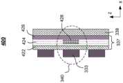
图4示出了3D NAND存储器400的示意性截面图,其包括与图3中的存储单元340相似的存储单元。存储单元340包括控制栅极(例如,控制栅极333)、存储膜(例如,存储膜337)和沟道层(例如,沟道层338,也称为沟道)。FIG. 4 shows a schematic cross-sectional view of a
在3D NAND存储器中,可以将存储膜337设置在(图3所示的)每个沟道孔336的侧壁上。在一些实施例中,存储膜337可以包括阻挡层422、储存层424和隧道层426。阻挡层422可以用于阻挡电荷载流子428在控制栅极333和储存层424之间的移动。阻挡层422可以包括氧化硅和高介电常数(高k)电介质,例如氧化铝。储存层424可以用于存储电荷载流子428,并且可以包括氮化硅。电荷载流子在储存层424中的存储和/或去除会影响沟道层338的开/关状态和/或电导率。隧道层426可用于控制电荷载流子428(电子或空穴)在沟道层338和储存层424之间的隧穿。隧道层426可以是氧化硅、氮化硅、氮氧化硅或其任意组合。在3D NAND存储器中,沟道层338可以设置在沟道孔336中的存储膜337的侧壁上(在图3中)。沟道层338可以包括非晶硅、多晶硅和/或单晶硅。In a 3D NAND memory, a
图5示出了根据本公开内容的一些实施例的存储块103(也称为存储阵列103)的示意性电路图。3D存储阵列103包括多个存储串212,每个存储串212具有多个存储单元340。存储串212在每一端还包括至少一个场效应晶体管(例如,MOSFET),分别由下选择栅极(LSG)332和上选择栅极(TSG)334控制。并且两个相应的晶体管被称为下选择晶体管332-T和上选择晶体管334-T。存储单元340可以由控制栅极333控制,其中一些控制栅极333可以被电连接到存储阵列103的相同字线。因此,为了简单起见,在本公开内容中可互换地使用控制栅极和它们的对应字线。上选择晶体管334-T的漏极端子可以连接到位线341,而下选择晶体管332-T的源极端子可以连接到阵列公共源极(ACS)430。ACS 430可以由整个存储块中的存储串212共享,并且也称为公共源极线。FIG. 5 shows a schematic circuit diagram of a memory block 103 (also referred to as a memory array 103 ) according to some embodiments of the present disclosure. The
在一些实施例中,存储阵列103可基于浮栅技术而形成。在一些实施例中,存储阵列103可基于电荷俘获技术而形成。基于电荷俘获的NAND闪存存储器可提供高存储密度和高固有可靠性。存储数据或逻辑状态(“状态”,例如,存储单元340的阈值电压Vth)取决于在存储层(例如,图4中的存储层424)中俘获的电荷载流子的数量。In some embodiments,
在NAND闪存存储器中,可以对包括共享相同字线的所有存储单元340的存储页432执行读操作和写操作(也称为编程操作),并且可以对存储块103执行擦除操作。In a NAND flash memory, read and write operations (also referred to as program operations) can be performed on a
参考图4与图5,在NAND存储器中,存储单元340可处于擦除状态ER或编程状态P1。最初,通过在控制栅极333和沟道338之间实现负电压差,可以将存储阵列103中的存储单元340复位到擦除状态ER作为逻辑“1”,使得可以去除存储单元340的存储层中的俘获电荷载流子。例如,可通过将存储单元340的控制栅极333设定到接地并将高正电压(擦除电压Verase)施加到ACS 430来诱发负电压差。在擦除状态ER(“状态ER”),存储单元340的阈值电压Vth可被复位为最低值。Referring to FIG. 4 and FIG. 5, in a NAND memory, the
在编程(即,写)期间,可通过(例如)在控制栅极333上施加编程电压Vpgm(例如,10V与20V之间的正电压脉冲)并使对应位线341接地来建立控制栅极333与沟道338之间的正电压差。结果,可以将电荷载流子(例如,电子)注入到存储单元340的存储层中,从而增加存储单元340的阈值电压Vth。因此,可以将存储单元340编程到经编程状态P1(“状态P1”)。During programming (i.e., writing), the control gate can be established by, for example, applying a programming voltage Vpgm (e.g., a positive voltage pulse between 10V and 20V) on the
存储单元的状态(例如,状态ER或状态P1)可通过测量或感测存储单元的阈值电压Vth来确定。在读操作期间,可以将读电压Vread施加在存储单元的控制栅极333上,并且可以在位线341处测量流过存储单元的电流。The state of the memory cell (eg, state ER or state P1 ) can be determined by measuring or sensing the threshold voltageVth of the memory cell. During a read operation, a read voltage Vread may be applied to the
NAND闪存存储器可被配置为在单级单元(SLC)模式中操作。为了增加存储容量,NAND闪存存储器还可被配置为在多级单元(MLC)模式、三级单元(TLC)模式、四级单元(QLC)模式或任意这些模式的组合中操作。在SLC模式中,存储单元存储1位且具有两个逻辑状态(“状态”),即,状态ER和P1。在MLC模式中,存储单元存储2位且具有四个状态,即,状态ER、P1、P2和P3。在TLC模式中,存储单元存储3位且具有八个状态,即状态ER和状态P1-P7。在QLC模式中,存储单元存储4位且具有16个状态。NAND flash memory can be configured to operate in single-level cell (SLC) mode. To increase storage capacity, NAND flash memory can also be configured to operate in multi-level cell (MLC) mode, triple-level cell (TLC) mode, quad-level cell (QLC) mode, or a combination of any of these modes. In SLC mode, a
因为相同存储页432中的存储单元340的控制栅极333电连接在一起作为字线(即,WL 333),所以由WL 333的偏置控制的编程操作影响相同存储页432中的所有存储单元340。因此,由所选WL寻址的未选存储单元经受编程干扰。类似地,由所选BL寻址的未选存储单元经受通过干扰。下面详细讨论编程干扰和通过干扰。Because the
当将编程电压Vpgm施加在所选WL 333-S上时,可将所选存储串212-S上的所选存储单元340-S编程为逻辑状态(例如,状态P1)。为了实现这一点,连接到所选存储串212-S的所选位线341-S可以接地,并且所选存储串212-S上的上选择晶体管334-T可以导通。可在未选存储单元333-U上施加通过电压Vpass以导通未选存储单元340-U。在一些实施例中,通过电压Vpass可以在6V和13V之间的范围内。当通过电压Vpass高于未选存储单元340-U的阈值电压Vth时,可以导通所选存储串212-S上的未选存储单元340-U。这样,所选存储串212-S的沟道338可以通过所选位线341-S连接到地。当将编程电压Vpgm施加在所选WL 333-S上时,控制栅极333与沟道338之间的大电位差导致电荷载流子(即,电子)隧穿到存储膜337中。通过调整编程电压Vpgm,可调整存储在存储膜337中的电荷载流子的数量。并且可相应地调整所选存储单元340-S的阈值电压Vth。这样,可将所选存储单元340-S编程到目标状态。The selected memory cells 340-S on the selected memory string 212-S may be programmed to a logic state (eg, state P1 ) when the programming voltage Vpgm is applied on the selected WL 333-S. To accomplish this, the selected bit line 341-S connected to the selected string 212-S may be grounded, and the upper select transistor 334-T on the selected string 212-S may be turned on. A pass voltage Vpass may be applied to the unselected memory cells 333-U to turn on the unselected memory cells 340-U. In some embodiments, the pass voltage Vpass may range between 6V and 13V. When the pass voltage Vpass is higher than the threshold voltage Vth of the unselected memory cells 340 -U, the unselected memory cells 340 -U on the selected memory string 212 -S may be turned on. In this way, the
在一些实施例中,在编程操作期间为所有未选WL 333-U选择单通过电压Vpass,其中单通过电压Vpass高于所有存储单元340的最大阈值电压Vth_max。虽然通过电压Vpass通常低于编程电压Vpgm,但通过电压Vpass也可引起电荷载流子的隧穿,从而在未选存储单元中引起阈值电压Vth的偏移ΔVth,且导致通过干扰。通过干扰随着编程操作的数量而累积,且可最终导致编程失败。In some embodiments, a single pass voltage Vpass is selected for all unselected WLs 333 -U during a program operation, wherein the single pass voltage Vpass is higher than the maximum threshold voltage Vth — max of all
类似地,在编程操作期间,不需要将连接到所选WL 333-S的所有存储单元340都编程到相同状态。当将编程电压Vpgm施加到所选WL 333-S上时,连接到所选WL 333-S的未选存储单元340-U经受编程干扰。可通过实施自升压技术来抑制编程干扰,其中可减小所选WL333-S与未选存储单元340-U的沟道338之间的正电压差并借此可减小负责电荷载流子的注入的电场。通过在连接到未选存储串212-U的未选位线341-U上施加禁止电压Vinhibit,可以实现自升压。在一些实施例中,禁止电压Vinhibit可以是在3V至5V之间的范围内的电源电压Vcc。在未选存储串212-U中,可以将上选择晶体管332-T导通,并且可以将下选择晶体管332-T关断。最初,未选存储串212-U的沟道可以通过未选位线341-U预充电。当将通过电压Vpass或编程电压Vpgm施加到未选存储单元340-U时,未选存储串212-U的沟道338的电位通过电容性耦合而上升,使得可以关断上选择晶体管332-T。随后,未选存储串212-U的沟道338变为浮置,并且沟道338的电位继续上升,直到变得非常接近(例如,大约80%的)通过电压Vpass或编程电压Vpgm。当将编程电压Vpgm施加到所选WL 333-S上时,沟道338的升高的电位阻止未选存储单元340-U中的电荷载流子隧穿。因此,通过在未选位线341-U上施加禁止电压Vinhibit,禁止对未选存储串212-U进行编程。Similarly, during a program operation, not all
虽然自升压在较高通过电压Vpass的情况下更有效,但如果通过电压Vpass过高,那么可对未选存储单元340-U进行编程,从而导致未选存储单元340-U的阈值电压Vth的偏移ΔVth。因此,为了抑制编程干扰和通过干扰,通过电压Vpass需要在特定范围内。在一些实施例中,可以确定最大通过电压Vpass_max以抑制通过干扰和编程干扰。Although self-boosting is more efficient at higher pass voltageVpass , if pass voltageVpass is too high, unselected memory cells 340-U can be programmed, resulting in a threshold of unselected memory cells 340-U The offset ΔVth of the voltage Vth . Therefore, in order to suppress program disturb and pass disturb, the pass voltage Vpass needs to be within a certain range. In some embodiments, a maximum pass voltage Vpass_max may be determined to suppress pass disturb and program disturb.
参考图3,由于制造过程中的工艺变化,沟道孔336(图3中)可具有不同的尺寸和形状。包括阻挡层422、存储层424和隧穿层426的存储膜337也可具有各种厚度和成分。在一些实施例中,工艺变化沿着垂直于衬底330的垂直方向(即,z方向)发展。例如,沟道孔336可以具有在底部(靠近衬底330)较小而在顶部(远离衬底330)较大的直径。并且存储膜337可以在底部较薄而在顶部较厚。因此,连接到不同字线(333-1、333-2、333-3)的存储单元340(例如,340-1、340-2、340-3)可在相同偏压条件下不同地表现。在一些实施例中,底部的存储单元可以经历阈值电压Vth的更大偏移ΔVth,因为它们更容易受到通过干扰的影响。当存储单元未保持在目标阈值电压Vth时,错误位增加。由通过干扰引起的阈值电压Vth的偏移随着编程周期的增加而增加。因此,基于对应存储单元对通过干扰的易受影响性(vulnerability),可以针对不同的字线实现不同的最大通过电压Vpass_max。Referring to FIG. 3 , the channel holes 336 (in FIG. 3 ) may have different sizes and shapes due to process variations in the manufacturing process. The
图6示出了根据本公开内容的一些实施例的存储块103的最大通过电压Vpass_max的实施方式。在该示例中,可将未选WL 333-U分离成两个或更多个WL组600,例如,第一WL组600-1、第二WL组600-2、第三WL组600-3、…等。每个WL组600可以包括一个或多个未选WL333-U。例如,第一WL组600-1包括第一未选WL 333-U集合。第二WL组600-2包括第二未选WL333-U集合。并且第三WL组600-3包括第三未选WL 333-U集合。每个WL组600中的未选WL333-U的数量可相同或不同。FIG. 6 illustrates an implementation of the maximum pass voltage Vpass_max of the
可以为相同WL组600中的未选WL 333-U指派相同最大通过电压Vpass_max。例如,第一WL组600-1中的第一未选WL 333-U集合可以具有第一最大通过电压Vpass_max-1,第二WL组600-2中的第二未选WL 333-U集合可以具有第二最大通过电压Vpass_max-2。第三WL组600-3中的第三未选WL 333-U集合可以具有第三最大通过电压Vpass_max-3。第一最大通过电压Vpass_max-1、第二最大通过电压Vpass_max-2和第三最大通过电压Vpass_max-3可以彼此相同或不同。在编程操作期间,可以向第一WL组600-1施加小于第一最大通过电压Vpass_max-1的第一通过电压Vpass_1;可以向第二WL组600-2施加小于第二最大通过电压Vpass_max-2的第二通过电压Vpass_2;可以向第三WL组600-3施加小于第三最大通过电压Vpass_max-3的第三通过电压Vpass_3。第一通过电压Vpass_1、第二通过电压Vpass_2和第三通过电压Vpass_3可以相同或不同。Unselected WLs 333 -U in the same WL group 600 may be assigned the same maximum pass voltage Vpass — max . For example, a first set of unselected WLs 333-U in the first WL group 600-1 may have a first maximum pass voltage Vpass_max-1 , a second set of unselected WLs 333-U in the second WL group 600-2 There may be a second maximum pass voltage Vpass — max-2 . A third unselected set of WLs 333-U in the third WL group 600-3 may have a third maximum pass voltage Vpass — max-3 . The first maximum pass voltage Vpass_max-1 , the second maximum pass voltage Vpass_max-2 , and the third maximum pass voltage Vpass_max -3 may be the same as or different from each other. During the program operation, a first pass voltage V pass_1 smaller than the first maximum pass voltage Vpass_max-1 may be applied to the first WL group600-1 ; a second maximum pass voltage V The second pass voltage Vpass_2 ofpass_max-2 ; the third pass voltage Vpass_3 smaller than the third maximum pass voltage Vpass_max-3 may be applied to the third WL group 600-3. The first pass voltage Vpass_1 , the second pass voltage Vpass_2 and the third pass voltage Vpass_3 may be the same or different.
可根据对应存储单元对通过干扰的易受影响性来分组未选WL 333-U。并且在编程操作之前,可以预先确定每个WL组600的最大通过电压Vpass_max。可以通过在具有通过电压Vpass的幅值的n个脉冲之后测量例如在状态ER中的阈值电压Vth的偏移ΔVth来确定每个WL333的易受影响性。图7A示出了根据本公开内容的一些实施例的状态ER的阈值电压Vth的偏移ΔVth与具有预先给定值V0(例如,12V)的通过电压Vpass的幅值的脉冲的数量的关系。可选择预先给定值V0,使得当通过电压Vpass=V0时,可使对由所选WL 333-S寻址的第四未选存储单元340-U集合的编程干扰最小。如所示的,当向第一WL组600-1、第二WL组600-2和第三WL组600-3施加具有预先给定值V0的相同通过电压Vpass时,由第一WL组600-1寻址的第一未选存储单元集合最易受通过干扰影响,即,经受阈值电压Vth的最大偏移ΔVth。在图7A中的示例中,阈值电压Vth的偏移ΔVth低于相应第二WL组600-2和第三WL组600-3中的第二和第三未选存储单元集合的最大允许偏移α。因此,第二最大通过电压Vpass_max-2和第三最大通过电压Vpass_max-3可以被确定为预先给定值V0。且第一WL组600-1的第一最大通过电压Vpass_max-1需要从预先给定值V0降低。Unselected WLs 333-U may be grouped according to the susceptibility of the corresponding storage units to pass-through interference. And before the program operation, the maximum pass voltage Vpass — max of each WL group 600 may be predetermined. The susceptibility of each
图7B示出了根据本公开内容的一些实施例的确定最大通过电压Vpass_max的方法。在该示例中,相对于具有通过电压Vpass的幅值的脉冲的数量而测量来自第一WL组600-1中的第一未选存储单元340-U集合的状态ER的阈值电压Vth的偏移ΔVth。在该测量中,通过电压Vpass从预先给定值V0递增地减小。当通过电压Vpass减小时,阈值电压Vth的偏移ΔVth减小。当阈值电压Vth的偏移ΔVth低于最大允许偏移α时,可以确定第一最大通过电压Vpass_max-1。这里,第一最大通过电压Vpass_max-1可以是V1,其中V1<V0。FIG. 7B illustrates a method of determining the maximum pass voltage Vpass_max according to some embodiments of the present disclosure. In this example, thethreshold voltage V of the state ER from the first unselected set of memory cells 340-U in the first WL group 600-1 is measured relative to the number of pulses having a magnitude of the pass voltage Vpass . Offset ΔVth . In this measurement, the pass voltage Vpass is incrementally reduced from a predetermined value V0 . When the pass voltage Vpass decreases, the shift ΔVth of the threshold voltage Vth decreases. The first maximum pass voltage V pass— max-1 may be determined when the shift ΔVth of the threshold voltage Vth is lower than the maximum allowable shift α. Here, the first maximum pass voltage Vpass_max-1 may be V1 , where V1 <V0 .
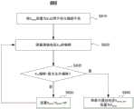
图8示出了根据本公开内容的一些实施例的用于确定每个WL组600的最大通过电压Vpass的方法800。应当理解,方法800中所示的步骤不是详尽无遗的,并且在所示步骤中的任何步骤之前、之后或之间也可以执行其它步骤。在一些实施例中,方法800的一些步骤可以省略或包括为了简单起见而未在此描述的其他步骤。在一些实施例中,方法800的步骤可以以不同的顺序执行和/或改变。FIG. 8 illustrates a
在步骤S810,将通过电压Vpass最初设置在预先给定值V0,其中选择预先给定值V0以使得对于连接到所选WL 333-S的第四未选存储单元340-U集合可使得编程干扰最小。如先前所论述,可使用自升压技术来抑制编程干扰。因为较高通过电压Vpass在自升压中和在抑制编程干扰中可以更有效,所以对于一些WL组(例如,底部处的更靠近衬底的WL组600-1)来说,预先给定值V0可能过高,这可导致例如第一未选存储单元340-U集合中的更多通过干扰。In step S810, the pass voltage Vpass is initially set at a predetermined value V0 , wherein the predetermined value V0 is selected such that it is available for the fourth set of unselected memory cells 340-U connected to the selected WL 333-S. Minimize programming interference. As previously discussed, self-boosting techniques can be used to suppress program disturb. Because a higher pass voltageVpass may be more effective in self-boosting and in suppressing program disturb, for some WL groups (eg, WL group 600-1 at the bottom closer to the substrate), it is predetermined that The value V0 may be too high, which may result in more passing disturbances in, for example, the first set of unselected memory cells 340-U.
在步骤S820,在具有通过电压Vpass的量值的n个脉冲之后测量第一WL组600-1中的第一未选存储单元340-U集合的阈值电压Vth。然后,在步骤S830,可以将阈值电压Vth的偏移ΔVth(例如,ER状态)与最大允许偏移α进行比较。In step S820, thethreshold voltage Vth of the first set of unselected memory cells 340-U in the first WL group 600-1 is measured after n pulses having a magnitude of the pass voltageVpass . Then, in step S830, the shift ΔVth (eg, ER state) of the threshold voltage Vth may be compared with the maximum allowable shift α.
如果偏移ΔVth小于最大允许偏移α,则在步骤S840,可以将瞬时通过电压Vpass设置为第一WL组600-1的第一最大通过电压Vpass_max-1。If the offset ΔVth is smaller than the maximum allowable offset α, at step S840, the instantaneous pass voltage Vpass may be set as the first maximum pass voltage Vpass_max-1 of the first WL group 600-1.
如果偏移ΔVth大于最大允许偏移α,则如步骤S850所示,可以将通过电压Vpass降低预定值dV,即,通过电压Vpass可以由新的值Vpass-dV代替。If the offset ΔVth is greater than the maximum allowable offset α, as shown in step S850 , the pass voltage Vpass may be reduced by a predetermined value dV, ie, the pass voltage Vpass may be replaced by a new value Vpass −dV.
在步骤S820再次测量WL组中的存储单元的阈值电压Vth,并且在步骤S830检查其偏移。重复步骤S850、S820和S830,直到满足步骤S830中的条件为止,在步骤S840可以确定第一WL组600的最大通过电压Vpass_max-1。The threshold voltageVth of the memory cell in the WL group is measured again at step S820, and its offset is checked at step S830. Steps S850 , S820 and S830 are repeated until the condition in step S830 is met, and in step S840 the maximum pass voltage Vpass — max−1 of the first WL group 600 may be determined.
通过执行图8中所示的方法,可以利用每个WL组600的优化的编程干扰和通过干扰来确定最大通过电压Vpass_max。By performing the method shown in FIG. 8 , the maximum pass voltage Vpass — max may be determined using optimized program disturb and pass disturb for each WL group 600 .
图9A示出了根据本公开内容的一些实施例的具有存储系统10的示例性系统900的框图。系统900可以是移动电话、台式计算机、膝上型计算机、平板计算机、车辆计算机、游戏控制台、打印机、定位设备、可穿戴电子设备、智能传感器、虚拟现实(VR)设备、增强现实(AR)设备或其中具有存储装置的任何其它合适的电子设备。存储系统10(也称为NAND存储系统)可以包括存储器控制器20和一个或多个存储器芯片25-1、25-2、25-3、…、25-n。每个半导体存储器芯片25(此后仅称为“存储器芯片”)可以是NAND芯片(即,“闪存”、“NAND闪存”或“NAND”)。存储系统10可通过存储器控制器20与主计算机15通信,其中存储器控制器20可经由一个或多个存储器通道30-1、30-2、30-3、…、30-n连接到一个或多个存储器芯片25-1、25-2、25-3、…、25-n。在一些实施例中,每个存储器芯片25可以由存储器控制器20经由存储器通道30来管理。FIG. 9A shows a block diagram of an
在一些实施例中,主计算机15可以包括电子设备的处理器,例如中央处理单元(CPU),或者片上系统(SoC),例如应用处理器(AP)。主计算机15发送要存储在NAND存储系统或存储系统10处的数据,或者通过读取存储系统10来提取数据。存储器控制器20可处理从主计算机15接收的I/O请求,确保数据完整性和有效存储,并管理存储器芯片25。存储器通道30可经由数据总线在存储器控制器20与每个存储器芯片25之间提供数据并控制通信。存储器控制器20可根据芯片启用信号选择存储器芯片25中的一个。In some embodiments, the
在一些实施例中,图9A中的每个存储器芯片25可以包括一个或多个存储器管芯100,其中每个存储器管芯可以类似于图1中所示的3D存储设备100。In some embodiments, each
存储器控制器20和一个或多个存储器芯片25可以集成到各种类型的存储设备中,例如,包括在相同的封装中,诸如通用闪存存储装置(UFS)封装或eMMC封装。即,存储系统10可以被实现和封装到不同类型的终端电子产品中。在如图9B所示的一个示例中,存储器控制器20和单个存储器芯片25可以集成到存储卡22中。存储卡22可以包括PC卡(PCMCIA,个人计算机存储卡国际协会)、CF卡、智能媒体(SM)卡、存储棒、多媒体卡(MMC、RS-MMC、MMCmicro)、SD卡(SD、miniSD、microSD、SDHC)、UFS等。存储卡22还可以包括将存储卡22与主机(例如,图9A中的主计算机15)耦合的存储卡连接器24。在如图9C所示的另一示例中,存储器控制器20和多个存储器芯片25可以集成到固态驱动器(SSD)26中。SSD 26可进一步包括将SSD 26与主机(例如,图9A中的主计算机15)耦合的SSD连接器28。The
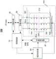
图10示出了根据本公开内容的一些实施例的存储器管芯100的示意图。存储器管芯100包括一个或多个存储块103。存储器管芯100的外围电路包括许多数字、模拟和/或混合信号电路以支持存储块103的功能,例如,页缓冲器50、字线驱动器40、控制电路70、电压发生器65和输入/输出缓冲器55。这些电路可以包括有源和/或无源半导体器件,例如晶体管、二极管、电容器、电阻器等,这对于本领域普通技术人员来说是显而易见的。FIG. 10 shows a schematic diagram of a memory die 100 according to some embodiments of the disclosure. Memory die 100 includes one or more memory blocks 103 . The peripheral circuitry of memory die 100 includes numerous digital, analog, and/or mixed-signal circuits to support the functions of
注意,图9A-C和图10中的存储系统10和存储器管芯100中的电子部件的布局作为示例示出。存储系统10和存储器管芯100可以具有其他布局并且可以包括附加部件。例如,存储器管芯100还可以具有读出放大器、列解码器等。存储系统10还可以包括固件、数据加扰器等。Note that the layout of the electrical components in
如图10所示,存储块103经由字线(例如,WL 333)和/或选择线(例如,LSG 332和TSG 334)与字线驱动器40耦合。存储块103经由位线(例如,BL 341)与页缓冲器50耦合。字线驱动器40可以响应于由控制电路70提供的控制信号来选择存储器管芯100上的存储块103中的一个。字线驱动器40可以根据控制信号将从电压发生器65提供的电压传输到字线。在编程操作期间,字线驱动器40可以根据从控制电路70接收的控制信号将编程电压Vpgm传输到所选字线并且将通过电压Vpass传输到未选字线。As shown in FIG. 10 ,
在编程操作期间,页缓冲器50可根据要编程的I/O数据向未选位线提供禁止电压Vinhibit并将所选位线接地。输入/输出缓冲器55可以将I/O数据传输到页缓冲器50,以及将输入地址或命令传输到控制电路70或字线驱动器40。During a program operation, the
控制电路70可以响应于由输入/输出缓冲器55传输的命令来控制页缓冲器50和字线驱动器40。在编程操作期间,控制电路70可以控制字线驱动器40和页缓冲器50以对所选存储单元进行编程。The
电压发生器65可以在控制电路70的控制下生成要提供给字线和位线的电压。由电压发生器65生成的电压包括编程电压Vpgm、通过电压Vpass、禁止电压Vinhibit。The
总之,本公开内容公开了一种用于对三维(3D)存储设备进行编程的方法。3D存储设备具有多个存储串,多个存储串具有垂直堆叠的存储单元,且每个存储单元可通过字线和位线寻址。对3D存储设备进行编程的方法包括以下步骤:在所选字线上施加编程电压;在第一组未选字线上施加第一通过电压;以及在第二组未选字线上施加第二通过电压,其中,第二通过电压不同于第一通过电压。In summary, the present disclosure discloses a method for programming a three-dimensional (3D) memory device. A 3D memory device has a plurality of memory strings with vertically stacked memory cells, and each memory cell is addressable through a word line and a bit line. The method for programming a 3D memory device comprises the steps of: applying a programming voltage on a selected word line; applying a first pass voltage on a first group of unselected word lines; and applying a second pass voltage on a second group of unselected word lines. A pass voltage, wherein the second pass voltage is different from the first pass voltage.
本公开内容还公开了一种三维(3D)存储设备。该3D存储设备包括多个存储单元,连接到被配置用于寻址多个存储单元中的每一个的字线和位线,其中,多个存储单元被垂直堆叠。3D存储设备还包括外围电路,被配置为编程所选存储单元。外围电路包括控制电路,被配置为将控制信号发送到字线驱动器。字线驱动器根据控制信号被配置为在所选字线上施加编程电压;在第一组未选字线上施加第一通过电压;以及在第二组未选字线上施加第二通过电压,其中,第二通过电压不同于第一通过电压。The present disclosure also discloses a three-dimensional (3D) storage device. The 3D memory device includes a plurality of memory cells connected to word lines and bit lines configured to address each of the plurality of memory cells, wherein the plurality of memory cells are vertically stacked. The 3D memory device also includes peripheral circuitry configured to program the selected memory cells. The peripheral circuit includes a control circuit configured to send a control signal to the word line driver. The word line driver is configured according to the control signal to apply a programming voltage on the selected word line; apply a first pass voltage on the first group of unselected word lines; and apply a second pass voltage on the second group of unselected word lines, Wherein, the second pass voltage is different from the first pass voltage.
本公开内容还公开了一种存储系统,其中,存储系统包括存储器控制器和存储器芯片(例如,三维存储设备)。存储器芯片包括连接到字线和位线的多个存储单元,字线和位线被配置用于寻址多个存储单元中的每一个,其中,多个存储单元被垂直堆叠。存储器芯片还包括外围电路,被配置为编程所选存储单元,外围电路包括控制电路。控制电路被配置为将控制信号发送到字线驱动器,其中,字线驱动器根据控制信号被配置为在所选字线上施加编程电压;在第一组未选字线上施加第一通过电压;以及在第二组未选字线上施加第二通过电压,其中,第二通过电压不同于第一通过电压。The present disclosure also discloses a storage system, wherein the storage system includes a memory controller and a memory chip (eg, a three-dimensional storage device). The memory chip includes a plurality of memory cells connected to word lines and bit lines configured to address each of the plurality of memory cells, wherein the plurality of memory cells are vertically stacked. The memory chip also includes peripheral circuitry configured to program the selected memory cells, the peripheral circuitry including control circuitry. The control circuit is configured to send a control signal to the word line driver, wherein the word line driver is configured to apply a programming voltage on the selected word line according to the control signal; apply a first pass voltage on the first group of unselected word lines; And applying a second pass voltage on the second group of unselected word lines, wherein the second pass voltage is different from the first pass voltage.
以上对具体实施例的描述将如此充分地揭示本公开内容的一般特征,以使得其他人可以通过应用本领域技术内的知识而针对各种应用容易地修改和/或适应这些具体实施例,无需过度实验,且不脱离本公开内容的一般概念。因此,基于本文给出的教导和指导,这样的适应和修改旨在处于所公开的实施例的等同变换的含义和范围内。应该理解的是,本文中的措辞或术语是出于描述的目的而非限制的目的,使得本说明书的术语或措辞将由本领域技术人员根据本公开内容和指导来解释。The above descriptions of specific embodiments will reveal the general characteristics of the present disclosure so fully that others can easily modify and/or adapt these specific embodiments for various applications by applying knowledge within the skill of the art without requiring Undue experimentation without departing from the general concept of the disclosure. Therefore, such adaptations and modifications are intended to be within the meaning and range of equivalents of the disclosed embodiments, based on the teaching and guidance presented herein. It should be understood that the words or phrases herein are for the purpose of description rather than limitation, such that the words or phrases of this specification will be construed by those skilled in the art in light of the present disclosure and guidance.
上面已经借助于功能构件块描述了本公开内容的实施例,该功能构件块示出了特定功能及其关系的实施方式。为了描述的方便,本文任意定义了这些功能构件块的边界。只要适当地执行了特定功能和关系,就可以定义可替换的边界。Embodiments of the present disclosure have been described above with the aid of functional building blocks that illustrate the implementation of specified functions and relationships thereof. For the convenience of description, the boundaries of these functional building blocks are arbitrarily defined herein. Alternate boundaries can be defined so long as the specified functions and relationships are appropriately performed.
发明内容和摘要部分可以阐述由发明人设想的本公开内容的一个或多个但不是全部的示例性实施例,并且因此不旨在以任何方式限制本公开内容和所附权利要求书。The Summary and Abstract sections may set forth one or more, but not all, exemplary embodiments of the disclosure contemplated by the inventors, and thus are not intended to limit the disclosure and the appended claims in any way.
本公开内容的广度和范围不应受任何上述示例性实施例的限制,而应仅根据下面的权利要求及其等同变换来限定。The breadth and scope of the present disclosure should not be limited by any of the above-described exemplary embodiments, but should be defined only in accordance with the following claims and their equivalents.
Claims (20)
Translated fromChinesePriority Applications (1)
| Application Number | Priority Date | Filing Date | Title |
|---|---|---|---|
| CN202310417300.9ACN116434805A (en) | 2021-04-01 | 2021-04-01 | Three-dimensional memory device, memory system including the same, and method of programming the same |
Applications Claiming Priority (3)
| Application Number | Priority Date | Filing Date | Title |
|---|---|---|---|
| CN202310417300.9ACN116434805A (en) | 2021-04-01 | 2021-04-01 | Three-dimensional memory device, memory system including the same, and method of programming the same |
| PCT/CN2021/084829WO2022205268A1 (en) | 2021-04-01 | 2021-04-01 | Programming for three-dimensional nand memory |
| CN202180001136.2ACN113228187B (en) | 2021-04-01 | 2021-04-01 | Three-dimensional memory device, memory system including the same, and method of programming the same |
Related Parent Applications (1)
| Application Number | Title | Priority Date | Filing Date |
|---|---|---|---|
| CN202180001136.2ADivisionCN113228187B (en) | 2021-04-01 | 2021-04-01 | Three-dimensional memory device, memory system including the same, and method of programming the same |
Publications (1)
| Publication Number | Publication Date |
|---|---|
| CN116434805Atrue CN116434805A (en) | 2023-07-14 |
Family
ID=77081262
Family Applications (2)
| Application Number | Title | Priority Date | Filing Date |
|---|---|---|---|
| CN202310417300.9APendingCN116434805A (en) | 2021-04-01 | 2021-04-01 | Three-dimensional memory device, memory system including the same, and method of programming the same |
| CN202180001136.2AActiveCN113228187B (en) | 2021-04-01 | 2021-04-01 | Three-dimensional memory device, memory system including the same, and method of programming the same |
Family Applications After (1)
| Application Number | Title | Priority Date | Filing Date |
|---|---|---|---|
| CN202180001136.2AActiveCN113228187B (en) | 2021-04-01 | 2021-04-01 | Three-dimensional memory device, memory system including the same, and method of programming the same |
Country Status (3)
| Country | Link |
|---|---|
| US (2) | US11887671B2 (en) |
| CN (2) | CN116434805A (en) |
| WO (1) | WO2022205268A1 (en) |
Family Cites Families (44)
| Publication number | Priority date | Publication date | Assignee | Title |
|---|---|---|---|---|
| US6269026B1 (en)* | 2000-02-29 | 2001-07-31 | Advanced Micro Devices, Inc. | Charge sharing to help boost the wordlines during APDE verify |
| US6917542B2 (en)* | 2003-07-29 | 2005-07-12 | Sandisk Corporation | Detecting over programmed memory |
| KR100922977B1 (en)* | 2007-12-27 | 2009-10-22 | 주식회사 하이닉스반도체 | Program Method of Nonvolatile Memory Device |
| KR101407361B1 (en)* | 2008-04-14 | 2014-06-13 | 삼성전자주식회사 | Non-volatile memory device and program method thereof |
| JP2011008838A (en)* | 2009-06-23 | 2011-01-13 | Toshiba Corp | Nonvolatile semiconductor memory device and writing method of the same |
| JP2014225310A (en)* | 2013-05-16 | 2014-12-04 | 株式会社東芝 | Nonvolatile semiconductor memory device |
| US9245637B2 (en)* | 2013-09-06 | 2016-01-26 | Sandisk Technologies Inc. | Systems and methods for read disturb management in non-volatile memory |
| CN110232942B (en)* | 2013-09-13 | 2023-01-03 | 铠侠股份有限公司 | Storage device and control method thereof |
| US9196366B2 (en)* | 2013-09-18 | 2015-11-24 | Winbond Electronics Corp. | Semiconductor memory apparatus and method for erasing the same |
| US9613713B2 (en)* | 2014-09-16 | 2017-04-04 | Kabushiki Kaisha Toshiba | Semiconductor memory device |
| KR20160136675A (en)* | 2015-05-20 | 2016-11-30 | 에스케이하이닉스 주식회사 | Semiconductor memory device and operating method thereof |
| US20170133099A1 (en)* | 2015-11-11 | 2017-05-11 | Fu-Chang Hsu | 3d nand array with divided string architecture |
| US9858995B1 (en)* | 2016-12-22 | 2018-01-02 | Macronix International Co., Ltd. | Method for operating a memory device |
| US10699767B2 (en)* | 2017-02-28 | 2020-06-30 | SK Hynix Inc. | Memory device and operating method thereof |
| KR20190023893A (en)* | 2017-08-30 | 2019-03-08 | 에스케이하이닉스 주식회사 | Semiconductor memory device and operating method thereof |
| TWI663602B (en)* | 2018-04-25 | 2019-06-21 | 旺宏電子股份有限公司 | Memory system and programming method |
| US10522232B2 (en)* | 2018-05-18 | 2019-12-31 | Sandisk Technologies Llc | Memory device with vpass step to reduce hot carrier injection type of program disturb |
| KR102461103B1 (en)* | 2018-07-10 | 2022-11-01 | 에스케이하이닉스 주식회사 | Memory device, memory system and operating method of memory device |
| KR102660057B1 (en)* | 2018-11-07 | 2024-04-24 | 삼성전자주식회사 | Nonvolatile memory device and method of programming in the same |
| KR102736207B1 (en)* | 2018-11-23 | 2024-12-02 | 에스케이하이닉스 주식회사 | Memory device and operating method thereof |
| US11276472B2 (en)* | 2018-12-12 | 2022-03-15 | Samsung Electronics Co., Ltd. | Non-volatile memory device and method of operating the same |
| CN209526877U (en) | 2018-12-29 | 2019-10-22 | 瑞声科技(新加坡)有限公司 | Loudspeaker |
| US11367493B2 (en)* | 2019-07-18 | 2022-06-21 | Samsung Electronics Co., Ltd. | Non-volatile memory devices and program methods thereof |
| CN110580928B (en)* | 2019-08-09 | 2021-08-17 | 长江存储科技有限责任公司 | A three-dimensional memory control method, device and storage medium |
| DE112019007666T5 (en)* | 2019-08-27 | 2022-06-15 | Micron Technology, Inc. | Write buffer control in a managed storage system |
| CN110892482B (en)* | 2019-10-12 | 2021-01-29 | 长江存储科技有限责任公司 | Method of programming a memory device and related memory device |
| CN110945591B (en)* | 2019-10-23 | 2021-01-29 | 长江存储科技有限责任公司 | Method of programming memory device and related memory device |
| KR20210089385A (en)* | 2020-01-08 | 2021-07-16 | 에스케이하이닉스 주식회사 | Memory device and operating method thereof |
| KR20210099936A (en)* | 2020-02-05 | 2021-08-13 | 에스케이하이닉스 주식회사 | Semiconductor memory device and operating method thereof |
| KR102782790B1 (en)* | 2020-03-06 | 2025-03-19 | 에스케이하이닉스 주식회사 | Memory device and operating method thereof |
| KR102788161B1 (en)* | 2020-03-24 | 2025-03-31 | 에스케이하이닉스 주식회사 | Semiconductor device and operating method of the semiconductor device |
| WO2021232223A1 (en) | 2020-05-19 | 2021-11-25 | Yangtze Memory Technologies Co., Ltd. | 3d nand flash and operation method thereof |
| KR20210143065A (en)* | 2020-05-19 | 2021-11-26 | 에스케이하이닉스 주식회사 | Semiconductor memory device and method for operating thereof |
| KR102760558B1 (en)* | 2020-05-21 | 2025-02-03 | 에스케이하이닉스 주식회사 | Memory device and operating method thereof |
| KR20210158216A (en)* | 2020-06-23 | 2021-12-30 | 에스케이하이닉스 주식회사 | Memory device and operating method thereof |
| US11653496B2 (en)* | 2020-09-25 | 2023-05-16 | Intel Corporation | Asymmetric junctions of high voltage transistor in NAND flash memory |
| US11315644B2 (en)* | 2020-09-25 | 2022-04-26 | Intel Corporation | String current reduction during multistrobe sensing to reduce read disturb |
| US11721397B2 (en)* | 2020-12-28 | 2023-08-08 | Sandisk Technologies Llc | Power saving and fast read sequence for non-volatile memory |
| US11322207B1 (en)* | 2020-12-30 | 2022-05-03 | Macronix International Co., Ltd. | Program method including multiple precharge steps for memory device |
| US12002522B2 (en)* | 2022-05-13 | 2024-06-04 | Macronix International Co., Ltd. | Memory device and operation method thereof |
| US11881271B2 (en)* | 2022-05-31 | 2024-01-23 | Sandisk Technologies Llc | Non-volatile memory with engineered channel gradient |
| KR20230168889A (en)* | 2022-06-08 | 2023-12-15 | 에스케이하이닉스 주식회사 | Memory device and operating method thereof |
| US12260921B2 (en)* | 2022-06-10 | 2025-03-25 | Sandisk Technologies Llc | Sense amplifier architecture providing reduced program verification time |
| JP2023184360A (en)* | 2022-06-17 | 2023-12-28 | キオクシア株式会社 | Semiconductor storage device and its control method |
- 2021
- 2021-04-01CNCN202310417300.9Apatent/CN116434805A/enactivePending
- 2021-04-01CNCN202180001136.2Apatent/CN113228187B/enactiveActive
- 2021-04-01WOPCT/CN2021/084829patent/WO2022205268A1/ennot_activeCeased
- 2021-11-04USUS17/518,783patent/US11887671B2/enactiveActive
- 2023
- 2023-12-12USUS18/537,263patent/US12272404B2/enactiveActive
Also Published As
| Publication number | Publication date |
|---|---|
| WO2022205268A1 (en) | 2022-10-06 |
| CN113228187A (en) | 2021-08-06 |
| US20240112739A1 (en) | 2024-04-04 |
| US11887671B2 (en) | 2024-01-30 |
| US12272404B2 (en) | 2025-04-08 |
| US20220319607A1 (en) | 2022-10-06 |
| CN113228187B (en) | 2023-05-05 |
Similar Documents
| Publication | Publication Date | Title |
|---|---|---|
| US12277993B2 (en) | Page buffer circuits in three-dimensional memory devices | |
| US11769559B2 (en) | Methods of reducing program disturb by array source coupling in 3D NAND memory devices | |
| US20240296894A1 (en) | Discharge circuits for a nand flash memory | |
| US11984193B2 (en) | Page buffer circuits in three-dimensional memory devices | |
| CN118173145A (en) | Three-dimensional NAND memory device and system and method of performing read operation thereof | |
| US20240427496A1 (en) | Method of improving programming operations in 3d nand systems | |
| CN113544785B (en) | Leak Detection for 3D NAND Memory | |
| US12260096B2 (en) | Method of reducing Vpass disturb in 3D nand systems | |
| US20240153547A1 (en) | Control method and system in 3d nand systems | |
| CN113228187B (en) | Three-dimensional memory device, memory system including the same, and method of programming the same | |
| US12211555B2 (en) | Memory device, memory system, and program method thereof | |
| US12254951B2 (en) | Memory device including page buffer, memory system including page buffer, and operating method thereof | |
| US20250232816A1 (en) | Memory devices and operation methods thereof | |
| CN117711465A (en) | 3D NAND storage device and control method thereof | |
| CN118262767A (en) | Power supply circuit and power supply method thereof |
Legal Events
| Date | Code | Title | Description |
|---|---|---|---|
| PB01 | Publication | ||
| PB01 | Publication | ||
| SE01 | Entry into force of request for substantive examination | ||
| SE01 | Entry into force of request for substantive examination |