CN116413956A - Lamp panel, manufacturing method thereof, backlight module and display device - Google Patents
Lamp panel, manufacturing method thereof, backlight module and display deviceDownload PDFInfo
- Publication number
- CN116413956A CN116413956ACN202310484977.4ACN202310484977ACN116413956ACN 116413956 ACN116413956 ACN 116413956ACN 202310484977 ACN202310484977 ACN 202310484977ACN 116413956 ACN116413956 ACN 116413956A
- Authority
- CN
- China
- Prior art keywords
- base substrate
- light source
- light
- reflective cup
- driving circuit
- Prior art date
- Legal status (The legal status is an assumption and is not a legal conclusion. Google has not performed a legal analysis and makes no representation as to the accuracy of the status listed.)
- Granted
Links
Images


Classifications
- G—PHYSICS
- G02—OPTICS
- G02F—OPTICAL DEVICES OR ARRANGEMENTS FOR THE CONTROL OF LIGHT BY MODIFICATION OF THE OPTICAL PROPERTIES OF THE MEDIA OF THE ELEMENTS INVOLVED THEREIN; NON-LINEAR OPTICS; FREQUENCY-CHANGING OF LIGHT; OPTICAL LOGIC ELEMENTS; OPTICAL ANALOGUE/DIGITAL CONVERTERS
- G02F1/00—Devices or arrangements for the control of the intensity, colour, phase, polarisation or direction of light arriving from an independent light source, e.g. switching, gating or modulating; Non-linear optics
- G02F1/01—Devices or arrangements for the control of the intensity, colour, phase, polarisation or direction of light arriving from an independent light source, e.g. switching, gating or modulating; Non-linear optics for the control of the intensity, phase, polarisation or colour
- G02F1/13—Devices or arrangements for the control of the intensity, colour, phase, polarisation or direction of light arriving from an independent light source, e.g. switching, gating or modulating; Non-linear optics for the control of the intensity, phase, polarisation or colour based on liquid crystals, e.g. single liquid crystal display cells
- G02F1/133—Constructional arrangements; Operation of liquid crystal cells; Circuit arrangements
- G02F1/1333—Constructional arrangements; Manufacturing methods
- G02F1/1335—Structural association of cells with optical devices, e.g. polarisers or reflectors
- G02F1/1336—Illuminating devices
- G02F1/133602—Direct backlight
- G02F1/133605—Direct backlight including specially adapted reflectors
- G—PHYSICS
- G02—OPTICS
- G02F—OPTICAL DEVICES OR ARRANGEMENTS FOR THE CONTROL OF LIGHT BY MODIFICATION OF THE OPTICAL PROPERTIES OF THE MEDIA OF THE ELEMENTS INVOLVED THEREIN; NON-LINEAR OPTICS; FREQUENCY-CHANGING OF LIGHT; OPTICAL LOGIC ELEMENTS; OPTICAL ANALOGUE/DIGITAL CONVERTERS
- G02F1/00—Devices or arrangements for the control of the intensity, colour, phase, polarisation or direction of light arriving from an independent light source, e.g. switching, gating or modulating; Non-linear optics
- G02F1/01—Devices or arrangements for the control of the intensity, colour, phase, polarisation or direction of light arriving from an independent light source, e.g. switching, gating or modulating; Non-linear optics for the control of the intensity, phase, polarisation or colour
- G02F1/13—Devices or arrangements for the control of the intensity, colour, phase, polarisation or direction of light arriving from an independent light source, e.g. switching, gating or modulating; Non-linear optics for the control of the intensity, phase, polarisation or colour based on liquid crystals, e.g. single liquid crystal display cells
- G02F1/133—Constructional arrangements; Operation of liquid crystal cells; Circuit arrangements
- G02F1/1333—Constructional arrangements; Manufacturing methods
- G02F1/1335—Structural association of cells with optical devices, e.g. polarisers or reflectors
- G02F1/1336—Illuminating devices
- G02F1/133602—Direct backlight
- G02F1/133603—Direct backlight with LEDs
- G—PHYSICS
- G02—OPTICS
- G02F—OPTICAL DEVICES OR ARRANGEMENTS FOR THE CONTROL OF LIGHT BY MODIFICATION OF THE OPTICAL PROPERTIES OF THE MEDIA OF THE ELEMENTS INVOLVED THEREIN; NON-LINEAR OPTICS; FREQUENCY-CHANGING OF LIGHT; OPTICAL LOGIC ELEMENTS; OPTICAL ANALOGUE/DIGITAL CONVERTERS
- G02F1/00—Devices or arrangements for the control of the intensity, colour, phase, polarisation or direction of light arriving from an independent light source, e.g. switching, gating or modulating; Non-linear optics
- G02F1/01—Devices or arrangements for the control of the intensity, colour, phase, polarisation or direction of light arriving from an independent light source, e.g. switching, gating or modulating; Non-linear optics for the control of the intensity, phase, polarisation or colour
- G02F1/13—Devices or arrangements for the control of the intensity, colour, phase, polarisation or direction of light arriving from an independent light source, e.g. switching, gating or modulating; Non-linear optics for the control of the intensity, phase, polarisation or colour based on liquid crystals, e.g. single liquid crystal display cells
- G02F1/133—Constructional arrangements; Operation of liquid crystal cells; Circuit arrangements
- G02F1/1333—Constructional arrangements; Manufacturing methods
- G02F1/1335—Structural association of cells with optical devices, e.g. polarisers or reflectors
- G02F1/1336—Illuminating devices
- G02F1/133602—Direct backlight
- G02F1/133608—Direct backlight including particular frames or supporting means
- Y—GENERAL TAGGING OF NEW TECHNOLOGICAL DEVELOPMENTS; GENERAL TAGGING OF CROSS-SECTIONAL TECHNOLOGIES SPANNING OVER SEVERAL SECTIONS OF THE IPC; TECHNICAL SUBJECTS COVERED BY FORMER USPC CROSS-REFERENCE ART COLLECTIONS [XRACs] AND DIGESTS
- Y02—TECHNOLOGIES OR APPLICATIONS FOR MITIGATION OR ADAPTATION AGAINST CLIMATE CHANGE
- Y02B—CLIMATE CHANGE MITIGATION TECHNOLOGIES RELATED TO BUILDINGS, e.g. HOUSING, HOUSE APPLIANCES OR RELATED END-USER APPLICATIONS
- Y02B20/00—Energy efficient lighting technologies, e.g. halogen lamps or gas discharge lamps
Landscapes
- Physics & Mathematics (AREA)
- Nonlinear Science (AREA)
- Mathematical Physics (AREA)
- Chemical & Material Sciences (AREA)
- Crystallography & Structural Chemistry (AREA)
- General Physics & Mathematics (AREA)
- Optics & Photonics (AREA)
- Devices For Indicating Variable Information By Combining Individual Elements (AREA)
- Planar Illumination Modules (AREA)
Abstract
Translated fromChinese
Description
Translated fromChinese技术领域technical field
本发明涉及显示技术领域,具体地说,涉及一种灯板及其制备方法、背光模组和显示装置。The invention relates to the field of display technology, in particular to a lamp panel, a preparation method thereof, a backlight module and a display device.
背景技术Background technique
背光模组为液晶显示面板的关键零组件之一,功能在于供应充足的亮度与分布均匀的光源,使其能正常显示影像。传统的背光模组中设置有灯板,通过灯板上分布的发光二极管(light emitting diode,LED)以及光散射结构实现均匀的背光。The backlight module is one of the key components of the liquid crystal display panel. Its function is to supply sufficient brightness and evenly distributed light source so that it can display images normally. A traditional backlight module is provided with a light board, and a uniform backlight is realized through light emitting diodes (light emitting diodes, LEDs) distributed on the light board and a light scattering structure.
一般而言,背光模组的发光效果将直接影响到液晶显示模组的视觉效果,背光模组依光源分布位置不同分为侧入式和直下式两种。直下式背光模组中LED的分区可以与液晶玻璃的分区一一对应,因此,局部调光效果较好,使得显示面板的画面动态对比度也较高。Generally speaking, the luminous effect of the backlight module will directly affect the visual effect of the liquid crystal display module. The backlight module is divided into side-type and direct-type according to the position of the light source. The partitions of the LEDs in the direct-lit backlight module can correspond to the partitions of the liquid crystal glass one-to-one. Therefore, the local dimming effect is better, and the dynamic contrast ratio of the display panel is also higher.
然而,直下式背光模组中,被点亮的LED之间会出现光线干扰,进而在显示面板上产生光晕现象,使得画面显示效果不佳。However, in the direct-lit backlight module, there will be light interference among the lit LEDs, and then a halo phenomenon will be generated on the display panel, resulting in a poor picture display effect.
需要说明的是,在上述背景技术部分公开的信息仅用于加强对本发明的背景的理解,因此可以包括不构成对本领域普通技术人员已知的现有技术的信息。It should be noted that the information disclosed in the above background technology section is only used to enhance the understanding of the background of the present invention, and therefore may include information that does not constitute prior art known to those of ordinary skill in the art.
发明内容Contents of the invention
有鉴于此,本发明提供一种灯板及其制备方法、背光模组和显示装置,以解决显示面板出现光晕导致显示画面不佳的问题。In view of this, the present invention provides a lamp panel and its preparation method, a backlight module and a display device, so as to solve the problem of poor display images caused by halos on the display panel.
根据本发明的一个方面,提供一种灯板,包括:According to one aspect of the present invention, a lamp panel is provided, comprising:
衬底基板,所述衬底基板上形成有反射杯和用于为光源供电的驱动线路;所述反射杯围合形成多个凹槽,所述反射杯的表面形成有反射层;所述衬底基板和所述反射杯均为玻璃材质;以及A base substrate, the base substrate is formed with a reflective cup and a driving circuit for powering the light source; the reflective cup surrounds and forms a plurality of grooves, and a reflective layer is formed on the surface of the reflective cup; the lining Both the base substrate and the reflector cup are made of glass; and
光源,所述光源布设于所述凹槽内,相邻两所述光源基于所述驱动线路实现电连接。The light source is arranged in the groove, and two adjacent light sources are electrically connected based on the driving circuit.
根据本发明的另一个方面,提供一种灯板的制备方法,包括以下步骤:According to another aspect of the present invention, a method for preparing a lamp panel is provided, comprising the following steps:
制备形成衬底基板和反射杯;所述反射杯围合形成多个凹槽;所述衬底基板和所述反射杯均为玻璃材质;Prepare and form a base substrate and a reflective cup; the reflective cup surrounds and forms a plurality of grooves; both the base substrate and the reflective cup are made of glass;
于所述衬底基板上制备形成用于为光源供电的驱动线路;Preparing and forming a driving circuit for powering the light source on the base substrate;
于所述反射杯的表面制备形成反射层;以及preparing and forming a reflective layer on the surface of the reflective cup; and
于所述凹槽内制备光源;相邻两所述光源基于所述驱动线路实现电连接。A light source is prepared in the groove; two adjacent light sources are electrically connected based on the driving circuit.
根据本发明的另一个方面,提供一种背光模组,包括上述任一灯板。According to another aspect of the present invention, a backlight module is provided, including any one of the above-mentioned lamp panels.
根据本发明的另一个方面,提供一种显示装置,包括上述背光模组。According to another aspect of the present invention, a display device is provided, including the above-mentioned backlight module.
本发明与现有技术相比的有益效果在于:The beneficial effect of the present invention compared with prior art is:
本发明提供的灯板及其制备方法、背光模组和显示装置基于对玻璃材质的基材加工成型形成反射杯,可以避免采用塑料基材加工成型反射杯,导致的光源开口精度难以控制,以及反射杯壁面曲面难以控制的问题,可以制作各种形状反射杯体结构,可以对光源光型进行任意二次设计,从而可以实现减弱显示面板产生的光晕现象,提升显示面板的显示效果。The lamp panel and its preparation method, backlight module and display device provided by the present invention are based on processing and molding glass substrates to form reflective cups, which can avoid the difficulty in controlling the accuracy of light source openings caused by processing and forming reflective cups with plastic substrates, and The curved surface of the reflective cup wall is difficult to control. Various shapes of reflective cup structures can be made, and the light pattern of the light source can be arbitrarily designed twice, so that the halo phenomenon generated by the display panel can be reduced and the display effect of the display panel can be improved.
附图说明Description of drawings
此处的附图被并入说明书中并构成本说明书的一部分,示出了符合本发明的实施例,并与说明书一起用于解释本发明的原理。显而易见地,下面描述中的附图仅仅是本发明的一些实施例,对于本领域普通技术人员来讲,在不付出创造性劳动的前提下,还可以根据这些附图获得其他的附图。The accompanying drawings, which are incorporated in and constitute a part of this specification, illustrate embodiments consistent with the invention and together with the description serve to explain the principles of the invention. Apparently, the drawings in the following description are only some embodiments of the present invention, and those skilled in the art can obtain other drawings according to these drawings without creative efforts.
图1为本发明一实施例公开的一种灯板的结构示意图;Fig. 1 is a schematic structural diagram of a lamp panel disclosed in an embodiment of the present invention;
图2为本发明一实施例公开的一种灯板上光源的光型示意图;Fig. 2 is a schematic diagram of the light pattern of a light source on a lamp panel disclosed by an embodiment of the present invention;
图3为本发明另一实施例公开的一种灯板上光源的光型示意图;Fig. 3 is a schematic diagram of the light pattern of a light source on a lamp panel disclosed in another embodiment of the present invention;
图4为现有技术中的灯板上光源的光型示意图;Fig. 4 is a schematic diagram of the light pattern of the light source on the lamp board in the prior art;
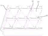
图5为本发明一实施例公开的于衬底基板上装配焊盘后的结构示意图;Fig. 5 is a schematic structural diagram after assembling pads on a base substrate disclosed by an embodiment of the present invention;
图6为本发明一实施例公开的光源装配完成后的结构示意图;Fig. 6 is a structural schematic diagram of the assembled light source disclosed by an embodiment of the present invention;
图7为本发明一实施例公开的灯板的局部剖视图;Fig. 7 is a partial cross-sectional view of a lamp panel disclosed by an embodiment of the present invention;
图8为本发明另一实施例公开的一种灯板的制备方法流程示意图;Fig. 8 is a schematic flowchart of a method for preparing a lamp panel disclosed in another embodiment of the present invention;
图9为本发明另一实施例公开的灯板的另一制备方法的流程示意图;Fig. 9 is a schematic flowchart of another preparation method of a lamp panel disclosed in another embodiment of the present invention;
图10为本发明另一实施例公开的灯板的另一制备方法的流程示意图;Fig. 10 is a schematic flowchart of another preparation method of a lamp panel disclosed in another embodiment of the present invention;
图11为本发明另一实施例公开的灯板的另一制备方法的流程示意图。Fig. 11 is a schematic flowchart of another manufacturing method of a lamp panel disclosed in another embodiment of the present invention.
附图标记reference sign
11、衬底基板;12、反射杯;13、凹槽;14、光源;15、焊盘;16、驱动线路;11. Substrate substrate; 12. Reflective cup; 13. Groove; 14. Light source; 15. Welding pad; 16. Drive circuit;
具体实施方式Detailed ways
为使本发明的上述目的、特征和优点能够更为明显易懂,下面将结合附图和实施例对本发明做进一步说明。In order to make the above objects, features and advantages of the present invention more comprehensible, the present invention will be further described below in conjunction with the accompanying drawings and embodiments.
需要说明的是,在以下描述中阐述了具体细节以便于充分理解本发明。但是本发明能够以多种不同于在此描述的其它方式来实施,本领域技术人员可以在不违背本发明内涵的情况下做类似推广。因此本发明不受下面公开的具体实施方式的限制。It should be noted that in the following description, specific details are set forth in order to fully understand the present invention. However, the present invention can be implemented in many other ways than those described here, and those skilled in the art can make similar extensions without departing from the connotation of the present invention. Accordingly, the present invention is not limited to the specific embodiments disclosed below.
在本发明实施例中使用的术语是仅仅出于描述特定实施例的目的,而非旨在限制本发明。在本发明实施例和所附权利要求书中所使用的单数形式的“一种”、“所述”和“该”也旨在包括多数形式,除非上下文清楚地表示其他含义。Terms used in the embodiments of the present invention are only for the purpose of describing specific embodiments, and are not intended to limit the present invention. As used in the embodiments of the present invention and the appended claims, the singular forms "a", "said" and "the" are also intended to include the plural forms unless the context clearly indicates otherwise.
需要注意的是,本发明实施例所描述的“上”、“下”、“左”、“右”等方位词是以附图所示的角度来进行描述的,不应理解为对本发明实施例的限定。此外在上下文中,还需要理解的是,当提到一个元件被形成在另一个元件“上”或“下”时,其不仅能够直接形成在另一个元件“上”或者“下”,也可以通过中间元件间接形成在另一元件“上”或者“下”。It should be noted that the orientation words such as "up", "down", "left", and "right" described in the embodiments of the present invention are described from the angles shown in the drawings, and should not be interpreted as a reference to the implementation of the present invention. Example limitations. Also in this context, it also needs to be understood that when it is mentioned that an element is formed "on" or "under" another element, it can not only be directly formed "on" or "under" another element, but also can be formed "on" or "under" another element. Formed "on" or "under" another element indirectly through intervening elements.
为使本发明的上述目的、特征和优点能够更为明显易懂,下面将结合附图和实施例对本发明做进一步说明。然而,示例实施方式能够以多种形式实施,且不应被理解为限于在此阐述的实施方式;相反,提供这些实施方式使得本发明更全面和完整,并将示例实施方式的构思全面地传达给本领域的技术人员。在图中相同的附图标记表示相同或类似的结构,因而将省略对它们的重复描述。本发明中所描述的表达位置与方向的词,均是以附图为例进行的说明,但根据需要也可以做出改变,所做改变均包含在本发明保护范围内。本发明的附图仅用于示意相对位置关系,某些部位的层厚采用了夸示的绘图方式以便于理解,附图中的层厚并不代表实际层厚的比例关系。且在不冲突的情况下,本发明中的实施例及实施例中的特征可以相互组合。本申请中各实施例的附图沿用了相同的附图的标记。In order to make the above objects, features and advantages of the present invention more comprehensible, the present invention will be further described below in conjunction with the accompanying drawings and embodiments. Example embodiments may, however, be embodied in many forms and should not be construed as limited to the embodiments set forth herein; rather, these embodiments are provided so that this disclosure will be thorough and complete, and will fully convey the concept of example embodiments to those skilled in the art. The same reference numerals denote the same or similar structures in the drawings, and thus their repeated descriptions will be omitted. The words expressing position and direction described in the present invention are all described by taking the accompanying drawings as an example, but changes can also be made according to needs, and all changes are included in the protection scope of the present invention. The accompanying drawings of the present invention are only used to illustrate the relative positional relationship, and the layer thickness of some parts is drawn in an exaggerated manner for easy understanding, and the layer thickness in the drawings does not represent the proportional relationship of the actual layer thickness. And in the case of no conflict, the embodiments and the features in the embodiments of the present invention can be combined with each other. The drawings of the various embodiments in this application continue to use the same reference numerals of the drawings.
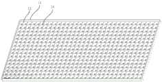
如图1、图5和图6所示,本发明实施例公开了一种灯板。上述灯板包括衬底基板11和光源14。其中,光源14基于焊盘15和衬底基板11连接。衬底基板11上形成有反射杯12,反射杯12的表面形成有反射层。反射杯12可以对光源14的光型起到二次设计的作用,利于减弱显示面板产生的光晕现象。参考图1,反射杯12呈交错排列的形式排布于衬底基板11上。相交的四面反射杯12围合形成凹槽13,上述光源14布设于该凹槽13内。As shown in FIG. 1 , FIG. 5 and FIG. 6 , the embodiment of the present invention discloses a lamp panel. The above lamp panel includes a
其中,上述光源14可以是发光二极管(LED)或者min-LED或者微发光二极管(micro-LED)中的一种,本发明对其具体类型不作限制。上述反射层可以采用喷涂、蒸镀或者印刷工艺制备形成,上述反射杯12的形状可以根据需要进行设置,比如可以为正方形或者矩形等;本发明对此均不作限制。Wherein, the above-mentioned
本实施例中,上述衬底基板11和反射杯12均为玻璃材质。相比于现有技术中通常采用塑料(比如PC聚碳酸酯材质)材质制备衬底基板11,本申请实施例可以避免吸水、热膨胀问题、高温老化问题、以及受材料限制导致反射率低的问题。In this embodiment, the
相比于现有技术中利用塑料材质结合注塑成型工艺或者吸塑成型工艺制备衬底基板11,本申请实施例可以避免模具设计复杂,不易脱模;光源14开口精度较难控制;反射杯12杯壁曲面较难控制等问题,具有降低模具设计复杂度、制备过程中容易控制光源14开口精度和反射杯12杯壁曲面等优点。Compared with the prior art that uses plastic material combined with injection molding process or blister forming process to prepare
在一些可选实施例中,上述反射杯12和衬底基板11基于一体成型工艺制备形成。一方面,相比于现有技术中基于组装工序将反射杯12和衬底基板11组装在一起形成灯板,导致存在工序复杂、反射杯12贴附过程难度大等问题,该实施例可以避免这些问题,具有制备效率高、难度低以及生产成本低的优点。In some optional embodiments, the
另一方面,基于一体成型工艺可以制作各种形状反射杯体结构,可以基于各种形状实现对光源14的光型的任意二次设计,从而可以实现减弱显示面板产生的光晕现象,提升显示面板的显示效果。On the other hand, based on the integrated molding process, various shapes of reflective cup structures can be produced, and any secondary design of the light pattern of the
参考图2和图3,其对应的是两种不同形状的反射杯12结构,那么灯板光源14发出的光型就不同。其中,图2中对应的反射杯体壁面为曲面结构,图3中对应的反射杯体壁面为平面结构。图2中的光晕减弱效果优于图3中的光晕减弱效果。Referring to Fig. 2 and Fig. 3, which correspond to two structures of
相比于图4所示的现有技术的灯板光源14发出的光型,本申请实施例中显示面板产生的光晕明显较小,因而利于提升显示面板的显示效果。Compared with the light pattern emitted by the lamp panel
本实施例中,衬底基板11上形成有用于为光源14供电的驱动线路16。衬底基板11上的相邻两个光源14基于上述驱动线路16实现电连接。具体实施时,在衬底基板11通过蚀刻等工艺形成供驱动线路16穿过的通道。该通道形成于衬底基板11的背面。上述通道的两端连通衬底基板11的同一侧。可以在通道内铺铜形成上述驱动线路。In this embodiment, a driving
参考图5和图6,上述凹槽13内设有焊盘15,焊盘15与蚀刻通道内的驱动线路电连接,比如可以以焊接的方式连接。焊盘15还与光源14的引脚电连接。上述焊盘15比如可以为基于焊锡形成,焊盘15固定连接于衬底基板11。示例性地,焊盘15可以基于焊接连接的方式固定连接于衬底基板11。需要说明的是,本申请对驱动线路的材质不以铜为限。Referring to FIG. 5 and FIG. 6 , a
具体而言,上述驱动线路16存在正负极之分,正极线连接于焊盘15形成正极连接端子,负极线连接于焊盘15形成负极连接端子。光源14的正极引脚就与该正极连接端子连接,光源14的负极引脚与该负极连接端子焊接连接,也即实现光源14与驱动线路16的电连接。Specifically, the driving
在衬底基板11的背面具体布线时,对所有光源14之间可以根据需要对一定数量范围内的光源采取并联或者串联的方式连接,可以在同一层玻璃中完成所有光源之间的连接,可以在其它层实现灯板的信号线以及数据线等的布线。本申请对其具体实现方式均不作限制。In the specific wiring on the back of the
需要说明的是,图7中示出的相邻两个光源基于两条线路实现连接,该相邻两个光源可以是一个光源的正极与另一个光源的正极连接,也可以是一个光源的正极与另一个光源的负极连接,本领域技术人员可以根据需要进行布线。并且,图7中示出的两条线路并不表示必然位于不同层玻璃中,可以位于同一层中。本申请对此均不作限制。It should be noted that the two adjacent light sources shown in Figure 7 are connected based on two lines, and the two adjacent light sources can be connected with the positive pole of one light source and the positive pole of the other light source, or can be the positive pole of one light source It is connected with the negative electrode of another light source, and those skilled in the art can perform wiring as required. Moreover, the two lines shown in FIG. 7 do not mean that they must be located in different layers of glass, but may be located in the same layer. This application is not limited to this.
并且,在将光源与驱动电源连接,以实现驱动电源向光源供电的布设过程中,驱动电源可以采取外挂的形式设置,也即独立于灯板且设置于灯板外部,不必设置于灯板的玻璃内,这样布设更加灵活。Moreover, in the process of connecting the light source with the driving power supply to realize the layout process of the driving power supplying power to the light source, the driving power supply can be installed in the form of a plug-in, that is, it is independent of the lamp board and installed outside the lamp board, and does not need to be installed on the lamp board. In the glass, the layout is more flexible.
在一可选实施例中,光源14设于衬底基板11的第一侧,沿着上述灯板的厚度方向,驱动线路16形成于衬底基板11的第二侧。也即,参考图7,驱动线路16位于反射杯12的杯壁曲面的下方,也位于光源14的下方。这样可以使得对上述通道的蚀刻难度更低。但是在其他实施例中,上述用于布设驱动线路16的通道也可以蚀刻形成于杯壁曲面上。本申请对此不作限制。In an optional embodiment, the
本实施例中,上述光源14的发光角度为140°-180°,且上述反射杯12的外壁沿着平行于灯板的厚度方向的截面符合贝塞尔曲线。也即,该截面与反射杯12的外壁面交叉形成的曲线符合贝塞尔曲线。参考图2,图2中所示的反射杯体壁面即为贝塞尔曲线结构,本申请实施例通过大发光角度的光源14配合呈贝塞尔曲线的反射杯12壁面,使原有光源的光型均匀分布以及收缩效果更好,提高光的利用效率的同时,利于进一步减弱显示面板产生的光晕现象,提升显示面板的显示效果。In this embodiment, the light emitting angle of the
本实施例中,上述反射层的反射率大于90%。也即,位于灯板正面的反射杯12中反射层采用高反射率涂料,这样也利于进一步减弱显示面板产生的光晕现象,提升显示面板的显示效果。本申请实施例在采用玻璃材质的反射杯上喷涂反射层,涂料更容易附着,并且反射层的抗变黄老化风险更小,从而利于延长其寿命。In this embodiment, the reflectivity of the reflective layer is greater than 90%. That is, the reflective layer in the
需要说明的是,本申请实施例对上述反射层的反射率以及光源14的发光角度均不作限定,本领域技术人员可根据需要进行设置。It should be noted that the embodiment of the present application does not limit the reflectivity of the above-mentioned reflective layer and the light emitting angle of the
本实施例中,上述光源14包括色彩转换膜和用于发射蓝光的蓝光芯片。上述色彩转换膜用于将上述蓝光芯片发出的蓝光转换为白光。具体实施时,色彩转换膜可以设置于蓝光芯片的上方。相比于现有技术中采用蓝光芯片和荧光粉搭配形成光源14的方案,本申请实施例具有色域更广,以及成本更低的优点。In this embodiment, the
本实施例中,上述凹槽13内填充有用于覆盖光源14的透光胶,通过该透光胶的设置可以保护光源14和焊盘15,防止污染、有毒气体侵蚀焊盘15,从而利于保证显示面板的显示效果。具体实施时,上述透光胶填充满上述凹槽,与反射杯的顶部平齐。In this embodiment, the above-mentioned
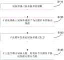
如图8所示,本发明另一实施例还公开了一种灯板的制备方法。该制备方法用于制备上述任一实施例公开的灯板。该制备方法包括步骤:As shown in FIG. 8 , another embodiment of the present invention also discloses a method for preparing a lamp panel. This preparation method is used to prepare the light board disclosed in any of the above embodiments. The preparation method comprises steps:
S110,制备形成衬底基板和反射杯。上述反射杯围合形成多个凹槽。S110, preparing and forming a base substrate and a reflective cup. The reflective cups surround and form a plurality of grooves.
S120,于衬底基板上制备形成用于为光源供电的驱动线路。S120, preparing and forming a driving circuit for powering the light source on the base substrate.
S130,于反射杯的表面制备形成反射层。S130, preparing and forming a reflective layer on the surface of the reflective cup.
以及S140,于上述凹槽内制备光源,相邻两个光源基于驱动线路实现电连接。And S140, preparing a light source in the groove, and electrically connecting two adjacent light sources based on the driving circuit.
步骤S110中,可以基于模具成型在衬底基板上形成反射杯。反射杯呈交错排列的形式排布于衬底基板上。其中,上述光源可以是发光二极管(LED)或者min-LED或者微发光二极管(micro-LED)中的一种,本发明对其具体类型不作限制。In step S110, a reflective cup may be formed on the base substrate based on mold molding. The reflective cups are arranged on the base substrate in a staggered arrangement. Wherein, the above-mentioned light source may be one of light-emitting diodes (LEDs) or min-LEDs or micro-LEDs (micro-LEDs), the specific types of which are not limited in the present invention.
步骤S130中,上述反射层可以采用喷涂、蒸镀或者印刷工艺制备形成,上述反射杯的形状可以根据需要进行设置,比如可以为正方形或者矩形等;本发明对此均不作限制。In step S130, the reflective layer can be formed by spraying, vapor deposition or printing process, and the shape of the reflective cup can be set as required, for example, it can be square or rectangular; the present invention is not limited thereto.
本实施例中,上述衬底基板和反射杯均为玻璃材质。相比于现有技术中通常采用塑料(比如PC聚碳酸酯材质)材质制备衬底基板,本申请实施例可以避免吸水、热膨胀问题、高温老化问题、以及受材料限制导致反射率低的问题。In this embodiment, the above-mentioned base substrate and reflective cup are made of glass. Compared with the usual plastic (such as PC polycarbonate) material used to prepare the base substrate in the prior art, the embodiment of the present application can avoid the problems of water absorption, thermal expansion, high temperature aging, and low reflectivity due to material limitations.
相比于现有技术中利用塑料材质结合注塑成型工艺或者吸塑成型工艺制备衬底基板,本申请实施例可以避免模具设计复杂,不易脱模;光源开口精度较难控制;反射杯杯壁曲面较难控制等问题,具有降低模具设计复杂度、制备过程中容易控制光源开口精度和反射杯杯壁曲面等优点。Compared with the prior art that uses plastic material combined with injection molding process or blister forming process to prepare the substrate substrate, the embodiment of the present application can avoid complex mold design and difficult demoulding; the opening precision of the light source is difficult to control; the curved surface of the reflective cup wall It is difficult to control and other problems, and has the advantages of reducing the complexity of mold design, easy to control the opening precision of the light source and the curved surface of the reflective cup wall during the manufacturing process.
步骤S140在具体实施时,光源和驱动线路可以分别布设于衬底基板的相对两侧。比如光源设于衬底基板的第一侧,驱动线路形成于衬底基板的第二侧。When step S140 is actually implemented, the light source and the driving circuit may be respectively arranged on opposite sides of the base substrate. For example, the light source is disposed on the first side of the base substrate, and the driving circuit is formed on the second side of the base substrate.
本实施例中,上述光源的发光角度为140°-180°,且上述反射杯的外壁沿着平行于灯板的厚度方向的截面符合贝塞尔曲线。也即,该截面与反射杯的外壁面交叉形成的曲线符合贝塞尔曲线。本申请实施例通过大发光角度的光源配合呈贝塞尔曲线的反射杯壁面,利于进一步减弱显示面板产生的光晕现象,提升显示面板的显示效果。In this embodiment, the light emitting angle of the above-mentioned light source is 140°-180°, and the section of the outer wall of the above-mentioned reflective cup along the thickness direction parallel to the light board conforms to a Bezier curve. That is, the curve formed by the intersection of the section and the outer wall of the reflective cup conforms to the Bezier curve. In the embodiment of the present application, a light source with a large light-emitting angle is combined with a Bezier-shaped reflective cup wall, which is beneficial to further reducing the halo phenomenon generated by the display panel and improving the display effect of the display panel.
本实施例中,上述反射层的反射率大于90%。也即,位于灯板正面的反射杯中反射层采用高反射率涂料,这样也利于进一步减弱显示面板产生的光晕现象,提升显示面板的显示效果。本申请实施例在采用玻璃材质的反射杯上喷涂反射层,涂料更容易附着,并且反射层的抗变黄老化风险更小,从而利于延长其寿命。In this embodiment, the reflectivity of the reflective layer is greater than 90%. That is to say, the reflective layer in the reflective cup located on the front of the lamp panel is made of high-reflectivity paint, which is also conducive to further reducing the halo phenomenon produced by the display panel and improving the display effect of the display panel. In the embodiment of the present application, the reflective layer is sprayed on the reflective cup made of glass, the paint is easier to adhere, and the risk of anti-yellowing and aging of the reflective layer is smaller, which is beneficial to prolonging its life.
需要说明的是,本申请实施例对上述反射层的反射率以及光源的发光角度均不作限定,本领域技术人员可根据需要进行设置。It should be noted that the embodiment of the present application does not limit the reflectivity of the above-mentioned reflective layer and the light emitting angle of the light source, and those skilled in the art can set them as required.
本实施例中,上述光源包括色彩转换膜和用于发射蓝光的蓝光芯片。上述色彩转换膜用于将上述蓝光芯片发出的蓝光转换为白光。具体实施时,色彩转换膜可以设置于蓝光芯片的上方。相比于现有技术中采用蓝光芯片和荧光粉搭配形成光源的方案,本申请实施例具有色域更广,以及成本更低的优点。In this embodiment, the above-mentioned light source includes a color conversion film and a blue light chip for emitting blue light. The above-mentioned color conversion film is used to convert the blue light emitted by the above-mentioned blue light chip into white light. During specific implementation, the color conversion film may be disposed above the blue light chip. Compared with the solution in the prior art that uses blue light chips and phosphors to form a light source, the embodiment of the present application has the advantages of wider color gamut and lower cost.
本实施例中,上述凹槽内填充有用于覆盖光源的透光胶,通过该透光胶的设置可以保护光源和焊盘,防止污染、有毒气体侵蚀焊盘,从而利于保证显示面板的显示效果。具体实施时,上述透光胶填充满上述凹槽,与反射杯的顶部平齐。In this embodiment, the above-mentioned groove is filled with light-transmitting glue for covering the light source, and the setting of the light-transmitting glue can protect the light source and the welding pad, prevent pollution and poisonous gas from eroding the welding pad, thereby helping to ensure the display effect of the display panel . During specific implementation, the above-mentioned light-transmitting glue fills the above-mentioned groove and is flush with the top of the reflective cup.
如图9所示,本发明另一实施例公开了另一种灯板的制备方法。该制备方法在上述图8对应实施例的基础上,将步骤S110替换为步骤S111:采用一体成型工艺制备形成衬底基板和反射杯。As shown in FIG. 9 , another embodiment of the present invention discloses another method for preparing a lamp panel. In this preparation method, on the basis of the above-mentioned embodiment corresponding to FIG. 8 , step S110 is replaced with step S111 : the base substrate and the reflective cup are prepared and formed by an integral molding process.
一方面,相比于现有技术中基于组装工序将反射杯和衬底基板组装在一起形成灯板,导致存在工序复杂、反射杯贴附过程难度大等问题,该实施例将反射杯结构与衬底基板一体设计,无需单独设计反射杯,从而可以避免这些问题,具有制备效率高、难度低以及生产成本低的优点。On the one hand, compared with the prior art where the reflective cup and the substrate are assembled together to form a lamp panel based on the assembly process, which leads to problems such as complicated procedures and difficult attaching process of the reflective cup, this embodiment combines the structure of the reflective cup with the The integrated design of the substrate and substrate eliminates the need to design a separate reflection cup, thereby avoiding these problems, and has the advantages of high preparation efficiency, low difficulty and low production cost.
另一方面,基于一体成型工艺可以制作各种形状反射杯体结构,可以对光源光型进行任意二次设计,从而可以实现减弱显示面板产生的光晕现象,提升显示面板的显示效果。On the other hand, based on the integrated molding process, various shapes of reflective cup structures can be produced, and the light source light pattern can be arbitrarily redesigned, so as to reduce the halo phenomenon generated by the display panel and improve the display effect of the display panel.
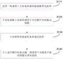
如图10所示,本发明另一实施例公开了另一种灯板的制备方法。该制备方法在上述图8对应实施例的基础上,将步骤S120替换为步骤S121:As shown in FIG. 10 , another embodiment of the present invention discloses another method for preparing a lamp panel. In this preparation method, on the basis of the embodiment corresponding to FIG. 8 above, step S120 is replaced by step S121:
于上述衬底基板制备形成供驱动线路穿过的通道,上述通道的两端连通衬底基板的同一侧,于该通道内布设驱动线路。A channel through which the driving circuit passes is prepared and formed on the base substrate, both ends of the channel communicate with the same side of the base substrate, and the driving circuit is arranged in the channel.
该实施例中,上述步骤S140包括:In this embodiment, the above step S140 includes:
S141,于上述凹槽内制备焊盘;驱动线路沿上述通道伸出于衬底基板,以与上述焊盘电连接。S141 , preparing pads in the above grooves; driving lines protruding from the base substrate along the channels so as to be electrically connected to the pads.
以及S142,基于上述焊盘在凹槽内制备光源。上述焊盘与上述光源的引脚电连接。And S142, preparing a light source in the groove based on the above pad. The pads are electrically connected to the pins of the light source.
步骤S121中,在衬底基板通过蚀刻等工艺形成供驱动线路穿过的通道,然后在通道内铺铜形成驱动线路。。该通道形成于衬底基板的背面。上述通道的两端连通衬底基板的同一侧。该步骤还包括:在凹槽内布设焊盘。该焊盘分别与驱动线路和光源电连接,比如可以以焊接的方式连接。焊盘布设完成后的效果图可参考图5。驱动线路的布设结构示意图可参考图7。In step S121 , a channel through which the driving circuit passes is formed on the base substrate through etching and other processes, and then copper is laid in the channel to form the driving circuit. . The channel is formed on the backside of the base substrate. Both ends of the above-mentioned channel communicate with the same side of the base substrate. This step also includes: arranging pads in the groove. The pads are respectively electrically connected to the driving circuit and the light source, for example, can be connected in a soldering manner. Refer to Figure 5 for the effect diagram after pad layout is completed. Refer to FIG. 7 for a schematic diagram of the layout structure of the driving circuit.
具体实施时,上述焊盘比如可以基于焊锡形成,焊盘固定连接于衬底基板。示例性地,焊盘可以基于焊接连接的方式固定连接于衬底基板。需要说明的是,本申请对驱动线路的材质不以铜为限。During specific implementation, the above-mentioned pads may be formed based on solder, for example, and the pads are fixedly connected to the base substrate. Exemplarily, the pads may be fixedly connected to the base substrate in a solder connection manner. It should be noted that, in this application, the material of the driving circuit is not limited to copper.
具体而言,上述驱动线路存在正负极之分,正极线连接于焊盘形成正极连接端子,负极线连接于焊盘形成负极连接端子。光源的正极引脚就与该正极连接端子连接,光源的负极引脚与该负极连接端子焊接连接,也即实现光源与驱动线路的电连接。Specifically, the above-mentioned driving circuit has positive and negative poles, the positive line is connected to the pad to form a positive connection terminal, and the negative line is connected to the pad to form a negative connection terminal. The positive pin of the light source is connected to the positive connecting terminal, and the negative pin of the light source is welded to the negative connecting terminal, that is, the electrical connection between the light source and the driving circuit is realized.
其中,光源和上述通道可以分别布设于衬底基板的相对两侧。比如光源设于衬底基板的第一侧,驱动线路和通道形成于衬底基板的第二侧。Wherein, the light source and the above-mentioned channels may be respectively arranged on opposite sides of the base substrate. For example, the light source is arranged on the first side of the base substrate, and the driving lines and channels are formed on the second side of the base substrate.
如图11所示,本发明另一实施例公开了另一种灯板的制备方法。该实施例中,反射杯位于上述衬底基板的第一侧。该制备方法在上述图8对应实施例的基础上,将步骤S120替换为步骤S122:As shown in FIG. 11 , another embodiment of the present invention discloses another method for preparing a lamp panel. In this embodiment, the reflective cup is located on the first side of the base substrate. In this preparation method, on the basis of the embodiment corresponding to FIG. 8 above, step S120 is replaced by step S122:
于上述衬底基板的第二侧制备形成驱动线路。上述衬底基板的第二侧与上述第一侧相对。A driving circuit is prepared and formed on the second side of the base substrate. The second side of the base substrate is opposite to the first side.
需要说明的是,本申请中公开的上述所有实施例可以进行自由组合,组合后得到的技术方案也在本申请的保护范围之内。It should be noted that all the above-mentioned embodiments disclosed in this application can be combined freely, and the technical solutions obtained after combination are also within the protection scope of this application.
本发明一实施例还提供一种背光模组,该背光模组包括上述任一实施例描述的灯板。其中,灯板的详细结构特征和优势可参照上述实施例的描述,此处不再赘述。可选地,上述背光模组为垂直向上发出光线的直下式背光模组。An embodiment of the present invention also provides a backlight module, which includes the lamp panel described in any one of the above embodiments. For the detailed structural features and advantages of the light board, reference may be made to the description of the above-mentioned embodiments, which will not be repeated here. Optionally, the above-mentioned backlight module is a direct-type backlight module that emits light vertically upward.
本发明一实施例还提供一种显示装置,该显示装置包括上述实施例描述的背光模组。An embodiment of the present invention also provides a display device, which includes the backlight module described in the above embodiments.
可以理解的,显示装置的类型可以为有机发光二极管(Organic Light-EmittingDiode,OLED)显示装置、QLED(Quantum Dot Light Emitting Diodes,量子点发光)显示装置或者micro LED(微发光二极管,μLED)显示装置等显示装置中的任意一种,本发明对此并不具体限制。It can be understood that the type of the display device may be an organic light-emitting diode (Organic Light-Emitting Diode, OLED) display device, a QLED (Quantum Dot Light Emitting Diodes, quantum dot light emitting) display device or a micro LED (micro light-emitting diode, μLED) display device Any one of the display devices, etc., the present invention is not specifically limited thereto.
上述实施例所提供的显示装置可以是显示不论运动(例如,视频)还是固定(例如,静止图像)的且不论文字还是的图像的任何装置。更明确地说,预期所述实施例可实施在多种电子装置中或与多种电子装置关联。所述多种电子装置例如(但不限于)移动电话、无线装置、个人数据助理(PDA)、手持式或便携式计算机、GPS接收器/导航器、相机、MP4视频播放器、摄像机、游戏控制台、手表、时钟、计算器、电视监视器、平板显示器、计算机监视器、汽车显示器(例如,里程表显示器等)、导航仪、座舱控制器和/或显示器、相机视图的显示器(例如,车辆中后视相机的显示器)、电子相片、电子广告牌或指示牌、投影仪、建筑结构、包装和美学结构等。The display device provided by the above-mentioned embodiments may be any device that displays images, whether moving (for example, video) or fixed (for example, still images), and regardless of text or images. More particularly, it is contemplated that the described embodiments may be implemented in or associated with a variety of electronic devices. Such various electronic devices as, but not limited to, mobile phones, wireless devices, personal data assistants (PDAs), handheld or portable computers, GPS receivers/navigators, cameras, MP4 video players, camcorders, game consoles , watches, clocks, calculators, television monitors, flat panel displays, computer monitors, automotive displays (e.g., odometer displays, etc.), navigators, cockpit controls and/or displays, camera view displays (e.g., rear view camera display), electronic photos, electronic billboards or signs, projectors, architectural structures, packaging and aesthetic structures, etc.
综上,本发明提供的灯板及其制备方法、背光模组和显示装置至少具有如下优势:To sum up, the lamp panel and its preparation method, backlight module and display device provided by the present invention have at least the following advantages:
本发明的实施例公开的灯板及其制备方法、背光模组和显示装置基于对玻璃材质的基材加工成型形成反射杯,可以避免采用塑料基材加工成型反射杯,导致的光源开口精度难以控制,以及反射杯壁面曲面难以控制的问题,可以制作各种形状反射杯体结构,可以对光源光型进行任意二次设计,从而可以实现减弱显示面板产生的光晕现象,提升显示面板的显示效果。The lamp board and its preparation method, backlight module and display device disclosed in the embodiments of the present invention are based on processing and molding a glass base material to form a reflective cup, which can avoid the difficulty in the accuracy of the light source opening caused by processing and forming a reflective cup with a plastic base material. Control, and the problem that the curved surface of the reflective cup wall is difficult to control, various shapes of reflective cup structures can be made, and the light pattern of the light source can be designed arbitrarily, so that the halo phenomenon generated by the display panel can be reduced and the display of the display panel can be improved. Effect.
以上内容是结合具体的优选实施方式对本发明所作的进一步详细说明,不能认定本发明的具体实施只局限于这些说明。对于本发明所属技术领域的普通技术人员来说,在不脱离本发明构思的前提下,还可以做出若干简单推演或替换,都应当视为属于本发明的保护范围。The above content is a further detailed description of the present invention in conjunction with specific preferred embodiments, and it cannot be assumed that the specific implementation of the present invention is limited to these descriptions. For those of ordinary skill in the technical field of the present invention, without departing from the concept of the present invention, some simple deduction or replacement can be made, which should be regarded as belonging to the protection scope of the present invention.
Claims (18)
Translated fromChinesePriority Applications (1)
| Application Number | Priority Date | Filing Date | Title |
|---|---|---|---|
| CN202310484977.4ACN116413956B (en) | 2023-04-28 | 2023-04-28 | Lamp panel, manufacturing method thereof, backlight module and display device |
Applications Claiming Priority (1)
| Application Number | Priority Date | Filing Date | Title |
|---|---|---|---|
| CN202310484977.4ACN116413956B (en) | 2023-04-28 | 2023-04-28 | Lamp panel, manufacturing method thereof, backlight module and display device |
Publications (2)
| Publication Number | Publication Date |
|---|---|
| CN116413956Atrue CN116413956A (en) | 2023-07-11 |
| CN116413956B CN116413956B (en) | 2025-08-15 |
Family
ID=87054536
Family Applications (1)
| Application Number | Title | Priority Date | Filing Date |
|---|---|---|---|
| CN202310484977.4AActiveCN116413956B (en) | 2023-04-28 | 2023-04-28 | Lamp panel, manufacturing method thereof, backlight module and display device |
Country Status (1)
| Country | Link |
|---|---|
| CN (1) | CN116413956B (en) |
Cited By (1)
| Publication number | Priority date | Publication date | Assignee | Title |
|---|---|---|---|---|
| CN117954564A (en)* | 2024-03-26 | 2024-04-30 | 深圳市佑明光电有限公司 | Mini LED backlight module without halation and preparation method thereof |
Citations (9)
| Publication number | Priority date | Publication date | Assignee | Title |
|---|---|---|---|---|
| CN101501870A (en)* | 2006-05-31 | 2009-08-05 | 株式会社藤仓 | Light-emitting device mounting substrate and method for producing same, light-emitting device module and method for manufacturing same, display, illuminating device, and traffic signal system |
| CN201844276U (en)* | 2010-07-27 | 2011-05-25 | 宁波市瑞康光电有限公司 | LED (light-emitting diode) backlight module, display and TV (television) |
| CN203190318U (en)* | 2013-04-01 | 2013-09-11 | 广州市鸿利光电股份有限公司 | Reflecting cup for LED light sources |
| TW201731128A (en)* | 2016-02-26 | 2017-09-01 | 光寶光電(常州)有限公司 | Photoelectric semiconductor device |
| CN110400519A (en)* | 2019-07-29 | 2019-11-01 | 京东方科技集团股份有限公司 | Backlight module, manufacturing method thereof, and display device |
| CN110703497A (en)* | 2019-10-09 | 2020-01-17 | 深圳市隆利科技股份有限公司 | Backlight device of surface light source and display apparatus |
| CN111061091A (en)* | 2019-12-31 | 2020-04-24 | 厦门天马微电子有限公司 | Optical module and display device |
| CN217788391U (en)* | 2022-06-23 | 2022-11-11 | 安徽繁盛显示科技有限公司 | Display panel based on ultrathin glass |
| KR20230000010A (en)* | 2021-06-23 | 2023-01-02 | 희성전자 주식회사 | Slim type back light unit |
- 2023
- 2023-04-28CNCN202310484977.4Apatent/CN116413956B/enactiveActive
Patent Citations (9)
| Publication number | Priority date | Publication date | Assignee | Title |
|---|---|---|---|---|
| CN101501870A (en)* | 2006-05-31 | 2009-08-05 | 株式会社藤仓 | Light-emitting device mounting substrate and method for producing same, light-emitting device module and method for manufacturing same, display, illuminating device, and traffic signal system |
| CN201844276U (en)* | 2010-07-27 | 2011-05-25 | 宁波市瑞康光电有限公司 | LED (light-emitting diode) backlight module, display and TV (television) |
| CN203190318U (en)* | 2013-04-01 | 2013-09-11 | 广州市鸿利光电股份有限公司 | Reflecting cup for LED light sources |
| TW201731128A (en)* | 2016-02-26 | 2017-09-01 | 光寶光電(常州)有限公司 | Photoelectric semiconductor device |
| CN110400519A (en)* | 2019-07-29 | 2019-11-01 | 京东方科技集团股份有限公司 | Backlight module, manufacturing method thereof, and display device |
| CN110703497A (en)* | 2019-10-09 | 2020-01-17 | 深圳市隆利科技股份有限公司 | Backlight device of surface light source and display apparatus |
| CN111061091A (en)* | 2019-12-31 | 2020-04-24 | 厦门天马微电子有限公司 | Optical module and display device |
| KR20230000010A (en)* | 2021-06-23 | 2023-01-02 | 희성전자 주식회사 | Slim type back light unit |
| CN217788391U (en)* | 2022-06-23 | 2022-11-11 | 安徽繁盛显示科技有限公司 | Display panel based on ultrathin glass |
Cited By (1)
| Publication number | Priority date | Publication date | Assignee | Title |
|---|---|---|---|---|
| CN117954564A (en)* | 2024-03-26 | 2024-04-30 | 深圳市佑明光电有限公司 | Mini LED backlight module without halation and preparation method thereof |
Also Published As
| Publication number | Publication date |
|---|---|
| CN116413956B (en) | 2025-08-15 |
Similar Documents
| Publication | Publication Date | Title |
|---|---|---|
| US11255524B2 (en) | Light emitting device | |
| TWI289366B (en) | Light source unit, illumination device using the same, and display device using the same | |
| US9223173B2 (en) | Lighting unit and display device having the same | |
| CN112863390A (en) | Light-emitting module, backlight module and display device | |
| US7671936B2 (en) | Liquid crystal display comprising at least one LED and a PCB and a frame having an opening with a narrow portion and a broad portion on a side surface of the frame and backlight module having the same | |
| CN102889507B (en) | Back light unit and use its display unit | |
| WO2019223202A1 (en) | Backlight module having surface light source, and liquid crystal display panel | |
| WO2021258489A1 (en) | Display panel and display device | |
| CN101520569A (en) | Power chip type LED light source for LCD backlight module | |
| CN101071232A (en) | Surface light source device, manufacturing method thereof, and liquid crystal display with the surface light source device | |
| CN101131502A (en) | Backlight module | |
| CN217639870U (en) | Backlight module, display module and display device | |
| CN114864797B (en) | Light-emitting panel and display device | |
| CN116413956A (en) | Lamp panel, manufacturing method thereof, backlight module and display device | |
| KR102718824B1 (en) | Display substrate and its manufacturing method and display device | |
| CN203363863U (en) | Straight down type backlight module and display device | |
| CN110838500B (en) | Micro light-emitting diode display device | |
| CN101520570A (en) | Light emitting device, backlight module and a flat panel display | |
| US20250085590A1 (en) | Backlight module, display module and display apparatus | |
| US20140071655A1 (en) | Direct Backlight Module | |
| JP4594859B2 (en) | LIGHTING DEVICE AND IMAGE DISPLAY DEVICE USING THE SAME | |
| WO2023025240A1 (en) | Light-emitting module and display device | |
| TWI384283B (en) | Backlight module with light emitting diode | |
| KR20130015744A (en) | Heat release printed circuit board, semiconductor illumination apparatus and display apparatus | |
| CN207799295U (en) | A kind of display module |
Legal Events
| Date | Code | Title | Description |
|---|---|---|---|
| PB01 | Publication | ||
| PB01 | Publication | ||
| SE01 | Entry into force of request for substantive examination | ||
| SE01 | Entry into force of request for substantive examination | ||
| GR01 | Patent grant | ||
| GR01 | Patent grant |