CN116404490A - Controlled impedance compressible connector - Google Patents
Controlled impedance compressible connectorDownload PDFInfo
- Publication number
- CN116404490A CN116404490ACN202211724272.7ACN202211724272ACN116404490ACN 116404490 ACN116404490 ACN 116404490ACN 202211724272 ACN202211724272 ACN 202211724272ACN 116404490 ACN116404490 ACN 116404490A
- Authority
- CN
- China
- Prior art keywords
- terminal
- housing
- movable
- center terminal
- electrical connector
- Prior art date
- Legal status (The legal status is an assumption and is not a legal conclusion. Google has not performed a legal analysis and makes no representation as to the accuracy of the status listed.)
- Pending
Links
- 230000013011matingEffects0.000claimsdescription73
- 239000012212insulatorSubstances0.000claimsdescription33
- 239000000758substrateSubstances0.000description14
- 239000004020conductorSubstances0.000description4
- 239000000463materialSubstances0.000description4
- 229910000906BronzeInorganic materials0.000description3
- OAICVXFJPJFONN-UHFFFAOYSA-NPhosphorusChemical compound[P]OAICVXFJPJFONN-UHFFFAOYSA-N0.000description3
- DMFGNRRURHSENX-UHFFFAOYSA-Nberyllium copperChemical compound[Be].[Cu]DMFGNRRURHSENX-UHFFFAOYSA-N0.000description3
- 239000010974bronzeSubstances0.000description3
- KUNSUQLRTQLHQQ-UHFFFAOYSA-Ncopper tinChemical compound[Cu].[Sn]KUNSUQLRTQLHQQ-UHFFFAOYSA-N0.000description3
- 238000004519manufacturing processMethods0.000description3
- 230000002349favourable effectEffects0.000description2
- 238000000034methodMethods0.000description2
- 229920001343polytetrafluoroethylenePolymers0.000description2
- 239000004810polytetrafluoroethyleneSubstances0.000description2
- 230000000712assemblyEffects0.000description1
- 238000000429assemblyMethods0.000description1
- 230000009286beneficial effectEffects0.000description1
- 230000007423decreaseEffects0.000description1
- -1polytetrafluoroethylenePolymers0.000description1
Images


Classifications
- H—ELECTRICITY
- H01—ELECTRIC ELEMENTS
- H01R—ELECTRICALLY-CONDUCTIVE CONNECTIONS; STRUCTURAL ASSOCIATIONS OF A PLURALITY OF MUTUALLY-INSULATED ELECTRICAL CONNECTING ELEMENTS; COUPLING DEVICES; CURRENT COLLECTORS
- H01R24/00—Two-part coupling devices, or either of their cooperating parts, characterised by their overall structure
- H01R24/38—Two-part coupling devices, or either of their cooperating parts, characterised by their overall structure having concentrically or coaxially arranged contacts
- H01R24/40—Two-part coupling devices, or either of their cooperating parts, characterised by their overall structure having concentrically or coaxially arranged contacts specially adapted for high frequency
- H01R24/42—Two-part coupling devices, or either of their cooperating parts, characterised by their overall structure having concentrically or coaxially arranged contacts specially adapted for high frequency comprising impedance matching means or electrical components, e.g. filters or switches
- H01R24/44—Two-part coupling devices, or either of their cooperating parts, characterised by their overall structure having concentrically or coaxially arranged contacts specially adapted for high frequency comprising impedance matching means or electrical components, e.g. filters or switches comprising impedance matching means
- H—ELECTRICITY
- H01—ELECTRIC ELEMENTS
- H01R—ELECTRICALLY-CONDUCTIVE CONNECTIONS; STRUCTURAL ASSOCIATIONS OF A PLURALITY OF MUTUALLY-INSULATED ELECTRICAL CONNECTING ELEMENTS; COUPLING DEVICES; CURRENT COLLECTORS
- H01R12/00—Structural associations of a plurality of mutually-insulated electrical connecting elements, specially adapted for printed circuits, e.g. printed circuit boards [PCB], flat or ribbon cables, or like generally planar structures, e.g. terminal strips, terminal blocks; Coupling devices specially adapted for printed circuits, flat or ribbon cables, or like generally planar structures; Terminals specially adapted for contact with, or insertion into, printed circuits, flat or ribbon cables, or like generally planar structures
- H01R12/70—Coupling devices
- H01R12/91—Coupling devices allowing relative movement between coupling parts, e.g. floating or self aligning
- H—ELECTRICITY
- H01—ELECTRIC ELEMENTS
- H01R—ELECTRICALLY-CONDUCTIVE CONNECTIONS; STRUCTURAL ASSOCIATIONS OF A PLURALITY OF MUTUALLY-INSULATED ELECTRICAL CONNECTING ELEMENTS; COUPLING DEVICES; CURRENT COLLECTORS
- H01R13/00—Details of coupling devices of the kinds covered by groups H01R12/70 or H01R24/00 - H01R33/00
- H01R13/02—Contact members
- H01R13/22—Contacts for co-operating by abutting
- H01R13/24—Contacts for co-operating by abutting resilient; resiliently-mounted
- H01R13/2407—Contacts for co-operating by abutting resilient; resiliently-mounted characterized by the resilient means
- H01R13/2421—Contacts for co-operating by abutting resilient; resiliently-mounted characterized by the resilient means using coil springs
- H—ELECTRICITY
- H01—ELECTRIC ELEMENTS
- H01R—ELECTRICALLY-CONDUCTIVE CONNECTIONS; STRUCTURAL ASSOCIATIONS OF A PLURALITY OF MUTUALLY-INSULATED ELECTRICAL CONNECTING ELEMENTS; COUPLING DEVICES; CURRENT COLLECTORS
- H01R13/00—Details of coupling devices of the kinds covered by groups H01R12/70 or H01R24/00 - H01R33/00
- H01R13/40—Securing contact members in or to a base or case; Insulating of contact members
- H01R13/42—Securing in a demountable manner
- H—ELECTRICITY
- H01—ELECTRIC ELEMENTS
- H01R—ELECTRICALLY-CONDUCTIVE CONNECTIONS; STRUCTURAL ASSOCIATIONS OF A PLURALITY OF MUTUALLY-INSULATED ELECTRICAL CONNECTING ELEMENTS; COUPLING DEVICES; CURRENT COLLECTORS
- H01R24/00—Two-part coupling devices, or either of their cooperating parts, characterised by their overall structure
- H01R24/38—Two-part coupling devices, or either of their cooperating parts, characterised by their overall structure having concentrically or coaxially arranged contacts
- H01R24/40—Two-part coupling devices, or either of their cooperating parts, characterised by their overall structure having concentrically or coaxially arranged contacts specially adapted for high frequency
- H01R24/42—Two-part coupling devices, or either of their cooperating parts, characterised by their overall structure having concentrically or coaxially arranged contacts specially adapted for high frequency comprising impedance matching means or electrical components, e.g. filters or switches
- H—ELECTRICITY
- H01—ELECTRIC ELEMENTS
- H01R—ELECTRICALLY-CONDUCTIVE CONNECTIONS; STRUCTURAL ASSOCIATIONS OF A PLURALITY OF MUTUALLY-INSULATED ELECTRICAL CONNECTING ELEMENTS; COUPLING DEVICES; CURRENT COLLECTORS
- H01R24/00—Two-part coupling devices, or either of their cooperating parts, characterised by their overall structure
- H01R24/38—Two-part coupling devices, or either of their cooperating parts, characterised by their overall structure having concentrically or coaxially arranged contacts
- H01R24/40—Two-part coupling devices, or either of their cooperating parts, characterised by their overall structure having concentrically or coaxially arranged contacts specially adapted for high frequency
- H01R24/50—Two-part coupling devices, or either of their cooperating parts, characterised by their overall structure having concentrically or coaxially arranged contacts specially adapted for high frequency mounted on a PCB [Printed Circuit Board]
- H—ELECTRICITY
- H01—ELECTRIC ELEMENTS
- H01R—ELECTRICALLY-CONDUCTIVE CONNECTIONS; STRUCTURAL ASSOCIATIONS OF A PLURALITY OF MUTUALLY-INSULATED ELECTRICAL CONNECTING ELEMENTS; COUPLING DEVICES; CURRENT COLLECTORS
- H01R24/00—Two-part coupling devices, or either of their cooperating parts, characterised by their overall structure
- H01R24/38—Two-part coupling devices, or either of their cooperating parts, characterised by their overall structure having concentrically or coaxially arranged contacts
- H01R24/40—Two-part coupling devices, or either of their cooperating parts, characterised by their overall structure having concentrically or coaxially arranged contacts specially adapted for high frequency
- H01R24/54—Intermediate parts, e.g. adapters, splitters or elbows
- H01R24/542—Adapters
- H—ELECTRICITY
- H01—ELECTRIC ELEMENTS
- H01R—ELECTRICALLY-CONDUCTIVE CONNECTIONS; STRUCTURAL ASSOCIATIONS OF A PLURALITY OF MUTUALLY-INSULATED ELECTRICAL CONNECTING ELEMENTS; COUPLING DEVICES; CURRENT COLLECTORS
- H01R12/00—Structural associations of a plurality of mutually-insulated electrical connecting elements, specially adapted for printed circuits, e.g. printed circuit boards [PCB], flat or ribbon cables, or like generally planar structures, e.g. terminal strips, terminal blocks; Coupling devices specially adapted for printed circuits, flat or ribbon cables, or like generally planar structures; Terminals specially adapted for contact with, or insertion into, printed circuits, flat or ribbon cables, or like generally planar structures
- H01R12/70—Coupling devices
- H01R12/7082—Coupling device supported only by cooperation with PCB
- H—ELECTRICITY
- H01—ELECTRIC ELEMENTS
- H01R—ELECTRICALLY-CONDUCTIVE CONNECTIONS; STRUCTURAL ASSOCIATIONS OF A PLURALITY OF MUTUALLY-INSULATED ELECTRICAL CONNECTING ELEMENTS; COUPLING DEVICES; CURRENT COLLECTORS
- H01R12/00—Structural associations of a plurality of mutually-insulated electrical connecting elements, specially adapted for printed circuits, e.g. printed circuit boards [PCB], flat or ribbon cables, or like generally planar structures, e.g. terminal strips, terminal blocks; Coupling devices specially adapted for printed circuits, flat or ribbon cables, or like generally planar structures; Terminals specially adapted for contact with, or insertion into, printed circuits, flat or ribbon cables, or like generally planar structures
- H01R12/70—Coupling devices
- H01R12/71—Coupling devices for rigid printing circuits or like structures
- H01R12/72—Coupling devices for rigid printing circuits or like structures coupling with the edge of the rigid printed circuits or like structures
- H01R12/73—Coupling devices for rigid printing circuits or like structures coupling with the edge of the rigid printed circuits or like structures connecting to other rigid printed circuits or like structures
- H—ELECTRICITY
- H01—ELECTRIC ELEMENTS
- H01R—ELECTRICALLY-CONDUCTIVE CONNECTIONS; STRUCTURAL ASSOCIATIONS OF A PLURALITY OF MUTUALLY-INSULATED ELECTRICAL CONNECTING ELEMENTS; COUPLING DEVICES; CURRENT COLLECTORS
- H01R13/00—Details of coupling devices of the kinds covered by groups H01R12/70 or H01R24/00 - H01R33/00
- H01R13/62—Means for facilitating engagement or disengagement of coupling parts or for holding them in engagement
- H01R13/629—Additional means for facilitating engagement or disengagement of coupling parts, e.g. aligning or guiding means, levers, gas pressure electrical locking indicators, manufacturing tolerances
- H01R13/631—Additional means for facilitating engagement or disengagement of coupling parts, e.g. aligning or guiding means, levers, gas pressure electrical locking indicators, manufacturing tolerances for engagement only
- H01R13/6315—Additional means for facilitating engagement or disengagement of coupling parts, e.g. aligning or guiding means, levers, gas pressure electrical locking indicators, manufacturing tolerances for engagement only allowing relative movement between coupling parts, e.g. floating connection
- H—ELECTRICITY
- H01—ELECTRIC ELEMENTS
- H01R—ELECTRICALLY-CONDUCTIVE CONNECTIONS; STRUCTURAL ASSOCIATIONS OF A PLURALITY OF MUTUALLY-INSULATED ELECTRICAL CONNECTING ELEMENTS; COUPLING DEVICES; CURRENT COLLECTORS
- H01R2103/00—Two poles
Landscapes
- Details Of Connecting Devices For Male And Female Coupling (AREA)
- Coupling Device And Connection With Printed Circuit (AREA)
Abstract
Translated fromChinese
Description
Translated fromChinese技术领域technical field
本发明涉及一种具有受控阻抗的可压缩同轴连接器或适配器。具体地说,本发明涉及一种可压缩同轴连接器或适配器,该可压缩同轴连接器或适配器保持有利的阻抗,同时适应配合基底之间的配合接合变化。The present invention relates to a compressible coaxial connector or adapter with controlled impedance. Specifically, the present invention relates to a compressible coaxial connector or adapter that maintains favorable impedance while accommodating changes in mating engagement between mating substrates.
背景技术Background technique
由于电子元件增加的复杂度,希望将更多的元件安装到电路板或其他基板上更小的空间内。因此,电路板中信号迹线和触头之间的空间已经缩小,然而电路板内容纳的信号迹线和触头的数量已经增加,从而增加了能够以越来越高的密度处理越来越高的速度的电连接器的需求。Due to the increasing complexity of electronic components, it is desirable to fit more components into less space on a circuit board or other substrate. As a result, the space between signal traces and contacts in circuit boards has shrunk, yet the number of signal traces and contacts housed within a circuit board has increased, increasing the ability to process increasingly higher and higher densities. Demand for high speed electrical connectors.
为两个配合连接器半部或电路板之间提供相互连接的共轴连接器和适配器在产业内是众所周知的。必须严格控制高速应用中使用的连接器内的阻抗,以便保持信号的完整性,特别是在微型RF连接器中。阻抗通过在整个连接器上保持内部导体与外部壳体之间的准确间距来控制。因为两个配合连接器半部或电路板之间的间距可由于制造公差等而变化,所以此类连接器和适配器需要能够顺应两个配合连接器半部或电路板之间的配合距离的变化。如美国专利号9,735,519中所描述的附接的电缆接触件允许接触件吸收两个配合连接器之间的配合距离的差异,因为至少一侧连接到电缆,该电缆可以与弹簧加载接触件一起相对于保持块(或模块)移动。对于两个配合连接器内的接触件连接到基板的应用,在所需配合距离变化内保持内导体与外导体之间的准确间距(以及因此阻抗)变得困难。Coaxial connectors and adapters that provide interconnection between two mating connector halves or circuit boards are well known in the industry. Impedance within connectors used in high-speed applications must be tightly controlled in order to maintain signal integrity, especially in miniature RF connectors. Impedance is controlled by maintaining accurate spacing between the inner conductor and outer housing throughout the connector. Because the spacing between the two mating connector halves or boards can vary due to manufacturing tolerances, etc., such connectors and adapters need to be able to accommodate changes in the mating distance between the two mating connector halves or boards . Attached cable contacts as described in U.S. Patent No. 9,735,519 allow the contacts to absorb differences in the mating distance between the two mating connectors as at least one side is connected to a cable which can be opposed together with the spring loaded contacts to keep the block (or module) moving. For applications where contacts in two mating connectors are connected to a substrate, maintaining the correct spacing (and thus impedance) between the inner and outer conductors over the required mating distance variation becomes difficult.
因此,有益的是提供一种同轴连接器或适配器,该同轴连接器或适配器可压缩以及能够在配合距离变化内保持阻抗,以稳定板对板连接的信号完整性。Accordingly, it would be beneficial to provide a coaxial connector or adapter that is compressible and capable of maintaining impedance over variations in mating distance to stabilize signal integrity for board-to-board connections.
发明内容Contents of the invention
一个实施例涉及一种受控阻抗可压缩电连接器,其具有壳体,壳体具有至少一个端子接收腔,至少一个端子接收腔从壳体的第一表面延伸到壳体的第二表面。端子组件定位在壳体的至少一个端子接收腔的每一个中。端子组件具有第一固定中心端子、第二可移动中心端子、固定外壳、可移动外壳和弹性构件。端子组件被配置为允许当第二可移动中心端子和可移动外壳相对于第一固定中心端子、固定外壳和壳体移动时保持电连接器的阻抗。One embodiment is directed to a controlled impedance compressible electrical connector having a housing having at least one terminal receiving cavity extending from a first surface of the housing to a second surface of the housing. A terminal assembly is positioned in each of the at least one terminal receiving cavity of the housing. The terminal assembly has a first fixed central terminal, a second movable central terminal, a fixed housing, a movable housing and a resilient member. The terminal assembly is configured to allow the impedance of the electrical connector to be maintained when the second movable center terminal and the movable housing move relative to the first fixed center terminal, the fixed housing and the housing.
一个实施例涉及一种用于在第一配合部件与第二配合部件之间提供电连接的受控阻抗可压缩电连接器。受控阻抗可压缩电连接器具有壳体,壳体具有至少一个延伸穿过壳体的端子接收腔。端子组件定位于至少一个端子接收腔内。端子组件包括固定中心端子、可移动外壳、可移动中心端子和弹性构件。可移动外壳可在至少一个端子接收腔和壳体中移动。可移动中心端子在可移动外壳中延伸。可移动中心端子与可移动外壳一致地移动。当可移动中心端子和可移动外壳移动时,保持可移动中心端子与可移动外壳之间的相对间距。弹性构件在可移动外壳上施加偏置力。可移动外壳和可移动中心端子相对于固定中心端子和壳体的移动允许受控阻抗可压缩电连接器顺应第一配合部件与第二配合部件之间的间距变化。当可移动中心端子和可移动外壳相对于固定中心端子和壳体移动时,保持电连接器的阻抗。One embodiment relates to a controlled impedance compressible electrical connector for providing an electrical connection between a first mating component and a second mating component. The controlled impedance compressible electrical connector has a housing with at least one terminal receiving cavity extending through the housing. A terminal assembly is positioned within at least one terminal receiving cavity. The terminal assembly includes a fixed central terminal, a movable housing, a movable central terminal and an elastic member. A movable housing is movable within the at least one terminal receiving cavity and the housing. A movable center terminal extends within the movable housing. The movable center terminal moves in unison with the movable housing. The relative spacing between the movable central terminal and the movable housing is maintained when the movable central terminal and the movable housing are moved. A resilient member exerts a biasing force on the movable housing. Movement of the movable housing and movable center terminal relative to the fixed center terminal and housing allows the controlled impedance compressible electrical connector to conform to changes in spacing between the first mating component and the second mating component. The impedance of the electrical connector is maintained when the movable center terminal and movable housing move relative to the fixed center terminal and housing.
通过下面结合附图对说明性实施例更加详细的描述,本发明的其它特征和优点将会变得明显,附图通过举例的方式说明本发明的原理。Other features and advantages of the invention will become apparent from the following more detailed description of the illustrative embodiments, taken in conjunction with the accompanying drawings, illustrating by way of example the principles of the invention.
附图说明Description of drawings
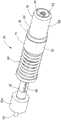
图1是用于说明性的共轴连接器系统中的适配器的接触件的说明性实施例的透视图。1 is a perspective view of an illustrative embodiment of a contact for an adapter in an illustrative coaxial connector system.
图2是图1的接触件的分解透视图。FIG. 2 is an exploded perspective view of the contact of FIG. 1 .
图3是沿着接触件的中心轴线截取的位于适配器壳体中的接触件的剖视图,示出了在与示例性固定基板配合之前的接触件和适配器。3 is a cross-sectional view of a contact in an adapter housing taken along a central axis of the contact, showing the contact and adapter prior to mating with an exemplary stationary substrate.
图4是类似于图3的接触件的剖视图,示出了与示例性固定基板部分配合的接触件和适配器。4 is a cross-sectional view of the contact similar to FIG. 3, showing the contact and adapter mated with an exemplary fixed substrate portion.
图5是接触件的剖视图,类似于图3,示出了与示例性固定基板完全配合的接触件和适配器。5 is a cross-sectional view of the contact, similar to FIG. 3 , showing the contact and adapter fully mated with an exemplary stationary substrate.
具体实施方式Detailed ways
如图3至图5所示,说明性受控阻抗可压缩电连接器或适配器10具有壳体12,壳体12具有至少一个端子接收腔14,至少一个端子接收腔14从壳体12的第一表面16延伸到壳体12的第二表面18。在所示的实施例中,壳体12是具有主体20和盖22的两件式壳体。然而,可使用壳体12的其他配置,包括但不限于单件壳体。As shown in FIGS. 3-5 , an illustrative controlled impedance compressible electrical connector or
第一肩部24从壳体12延伸到端子接收腔14中。在所示的示例性实施例中,第一肩部24关于端子接收腔14的整个圆周向内延伸。然而,可以使用第一肩部24的其他配置。第一肩部24位于第一表面16和第二表面18之间。The
第二肩部26从壳体12延伸到端子接收腔14中。在所示的示例性实施例中,第二肩部26关于端子接收腔14的整个圆周向内延伸。然而,可以使用第二肩部26的其他配置。第二肩部26定位在第一表面与第二表面之间并且接近第一表面16。在所示的实施例中,第二肩部26设置在壳体12的盖22上。The
端子组件30定位在壳体的至少一个端子接收腔14的每一个中。如图1和图2所示,端子组件30中的每一个包括第一固定中心端子32、第二可移动中心端子34、固定外壳36、可移动外壳38、弹性构件或弹簧40以及绝缘体42。A
第一固定中心端子32具有第一配合部段44和第二配合部段46。在示出的说明性实施例中,第一配合部段44是插针,并且在远离第一表面16的方向上从第二表面18延伸。第一配合部段44被配置为完成到基板的电连接(未示出)。第二配合部段46是用于在其中接收第二可移动中心端子34的端部的阴型接收部。绝缘体42a位于第一配合部段44和第二配合部段46之间。绝缘体42a围绕第一固定中心端子32的圆周延伸。绝缘体42a的尺寸被设定成从第一固定中心端子32延伸到端子接收腔14的壁48。绝缘体42a将第一固定中心端子32适当地定位在端子接收腔14中并且将第一固定中心端子32保持在其中。在所示的说明性实施例中,第一固定中心端子32由铍铜形成,但是也可以使用具有适当导电和强度特性的其他材料,例如但不限于磷青铜。绝缘体42a可以由聚四氟乙烯(PTFE)或其他具有适当绝缘和强度特性的材料制成。The first fixed
第二可移动中心端子34具有第一配合部段50和第二配合部段52。在示出的说明性实施例中,第一配合部段50是插针。第一配合部段50被配置为与第一固定中心端子32的第二配合部段46进行电连接。第二可移动中心端子34的第二配合部段52是用于接收第二基底56的配合接触件54的端部的阴型接收部。第二可移动中心端子34具有不同直径的部段,包括第一减小直径部段58和第二减小直径部段60。在所示的说明性实施例中,第二可移动中心端子34由铍铜形成,但是也可以使用具有适当导电和强度特性的其他材料,例如但不限于磷青铜。The second
第二绝缘体42b定位在第一减小直径部段58中。第二绝缘体42b围绕第一减小直径部段58的圆周延伸。第二绝缘体42a的尺寸被设定成从第二可移动中心端子34延伸到可移动外壳38。第二绝缘体42b将第二可移动中心端子34适当地定位在可移动外壳38中并且将第二可移动中心端子34保持在其中。The
第三绝缘体42c与第二减小直径部段60配合。第三绝缘体42c围绕第二减小直径部段60的圆周延伸。第三绝缘体42c的尺寸被设定成从第二可移动中心端子34延伸到可移动外壳38。第三绝缘体42c将第二可移动中心端子34适当地定位在可移动外壳38中并且将第二可移动中心端子34保持在其中。The
固定外壳36具有导电壁62和后壁64。导电壁62和后壁64形成第一端子接收腔66。第一端子接收腔66尺寸被设定为在其中接收第二可移动中心端子34的第一配合部段50和可移动外壳38的一部分。后壁64具有开口68,开口68的尺寸被设定成允许第二可移动中心端子34的第一配合部段50延伸穿过该开口68并且与第一固定中心端子32的第二配合部段46配合。安装肩部或突出部70从导电壁62在远离第一端子接收腔66的方向上延伸。安装突出部70与壳体12的第一肩部24协作,以将固定外壳36适当地定位并固定在端子接收腔14中。The
在所示说明性实施例中,可移动外壳38包括第一可移动外壳74和第二可移动外壳76。然而,可以使用可移动外壳38的其他配置。在示出的说明性实施例中,第一可移动外壳74和第二可移动外壳76由铍铜形成,但是也可以使用具有适当导电和强度特性的其他材料,例如但不限于磷青铜。In the illustrative embodiment shown,
第一可移动外壳74具有带有导电外壁77的管状配置。外壁77具有第一内径为D1的第一端子接收部分78、第二内径为D2的第二端子接收部分80以及第三内径为D3的第三端子接收部分82。第三内径D3大于第二内径D2,并且第二内径D2大于D1的第一内径。The first
第一端子接收部分78被配置为接收第二可移动中心端子34的第一减小直径部段58。第二端子接收部分80被配置为接收第一减小直径部段58和第二绝缘体42b。第二端子接收部分80与第二绝缘体42b协作,以将第二可移动中心端子34适当定位在可移动外壳38中并且将第二可移动中心端子34保持在其中。第三端子接收部段82被配置为接收第二可移动中心端子34和第二可移动外壳76的一部分。The first
第二可移动外壳76具有带有导电外壁84的管状配置。外壁84具有内径为D4的第一端子接收部分86和内径为D5的第二端子接收部分88。内径D4略大于内径D5。在所示说明性实施例中,内径D5大致等于第一可移动外壳74的第三内径D2,然而,可使用其他配置。The second
第二可移动外壳76的第二端子接收部分88被配置为接收第二可移动中心端子34的第二配合部段52。第二可移动外壳76的第一端子接收部分86被配置为接收第二可移动中心端子34的接近第二配合部段52的部分。第一端子接收部分86还被配置为接收第三绝缘体42c。第一端子接收部分86的肩部90与第三绝缘体42c协作,以将第二可移动中心端子34适当地定位在可移动外壳38中并且将第二可移动中心端子34保持在其中。第一端子接收部分86还被配置为接收在第一可移动外壳74的第三端子接收部段82中。第二可移动外壳76上设置有外突出部或肩部92,以便于第二可移动外壳76相对于第一可移动外壳74的适当定位。The second
弹簧40在固定外壳36和可移动外壳74之间延伸。在所示的实施例中,弹簧40在固定外壳36的安装突出部70与可移动外壳38的第一可移动外壳74的肩部94之间延伸。
在与配合连接器或基板56配合之前,连接器或适配器10处于图3所示的位置中。在这个位置中,第一固定中心端子32的第一配合部段44延伸超出壳体12的第二表面18。第二可移动外壳76的第二端子接收部分88和第二可移动中心端子34的第二配合部段52延伸超出壳体12的第一表面18。虽然在这个实施例中,第一固定中心端子32的第一配合部段44延伸超出壳体12的第二表面18,但是可使用第一配合部段44其他配置,诸如用于表面安装应用。Prior to mating with a mating connector or
在图3所示的位置中,第二可移动中心端子34的第一配合部段50的末端部分定位在第一固定中心端子32的第二配合部段46中。第一配合部段50的剩余部分定位在固定外壳36的端子接收腔66中。可移动外壳38的第一可移动外壳74的第一端子接收部分78的末端部分也定位在固定外壳36的端子接收腔66中。In the position shown in FIG. 3 , the end portion of the
在这个位置中,弹簧40保持在稍微压缩的位置中。因此,弹簧40在安装突出部70上施加力以将固定外壳36偏置抵靠壳体10的第一肩部24。此外,弹簧40在可移动外壳38的第一可移动外壳74的肩部94上施加力以将第二可移动外壳76的突出部92偏置抵靠壳体的第二肩部26。在这样做时,端子组件30通过弹簧40的力维持在其初始或未配合的位置中。在初始或未配合位置中,在壳体12的第一肩部24与第一可移动外壳74的导电外壁77的自由端69之间的端子接收腔66中提供空间或凹腔67。In this position, the
当适配器10和端子组件30移动成与第二基板56接合时,第二可移动外壳76的第二端子接收部分88移动成与第二基板56上的外壳55接合,如图4所示。此外,第二可移动中心端子34的第二配合部段52移动到与第二基板56的配合接触件54接合。这样做,在基板56与适配器10之间建立同轴电连接。When the
当完全插入时,如图5所示,第二可移动外壳76的第二端子接收部分88和第二可移动中心端子34的第二配合部段52被迫朝向壳体12的第二表面18向内移动。当这发生时,整个端子组件30从图3所示的位置向壳体12的第二表面18移动,如图5所示。When fully inserted, as shown in FIG. Move inward. When this occurs, the entire
当端子组件30移动到图5所示的位置时。固定外壳36和第一固定中心端子32保持静止并且不移动。然而,端子组件30的其余部分(包括第二可移动端子38、第一可移动外壳74和第二可移动外壳76)一致地移动。因此,当端子组件30在端子接收腔14中移动或滑动时,第二可移动中心端子34相对于第一可移动外壳74和第二可移动外壳76的定位和间距不改变。这允许在适配器10与配合连接器或基板配合时适当地控制和维持端子组件30的阻抗。When the
特别是,当端子组件30从图3所示的第一位置移动到图5所示的第二位置时:保持第二可移动中心端子34的减小直径部段58相对于第一可移动外壳74的第一端子接收部分78的定位和间距;保持第二可移动中心端子34的减小直径部段58和第二绝缘体42b相对于第一可移动外壳74的第二端子接收部分80的定位和间距;保持第二可移动中心端子34的第二配合部段52相对于第二可移动外壳76的第二端子接收部分88的定位和间距;以及保持第二可移动中心端子34的接近第二配合部段52的部分和第三绝缘体42c相对于第二可移动外壳76的第二端子接收部分88的定位和间距。In particular, when the
以下各部段的配置以及尤其是间距被计算使得这些部段中的每一个中的阻抗与其他部段中的每一个中的阻抗匹配:在第一可移动外壳74的第一端子接收部分78中的第二可移动中心端子34的减小直径部段58;在第一可移动外壳74的第二端子接收部分80中的第二可移动中心端子34的减小直径部段58和第二绝缘体42b;在第二可移动外壳76的第二端子接收部分88中的第二可移动中心端子34的第二配合部段52;以及在第二可移动外壳76的第二端子接收部分88中的第二可移动中心端子34的接近第二配合部段52的部段和第三绝缘体42c。这允许信号在信号完整性较少损失或没有损失的情况下跨每个部段和跨端子组件30传输。The configuration and especially the spacing of the following sections are calculated such that the impedance in each of these sections matches the impedance in each of the other sections: In the first
在端子组件30从图1所示的第一位置移动到图5所示的第二位置期间,第二可移动中心端子34的第一配合部段50从固定外壳36的第一接收腔66移动到第一固定中心端子32的第二配合部段46中。当这种情况发生时,当导电外壁77的自由端69朝向壳体12的第一肩部24移动时,空间或凹腔67的大小减小。固定外壳36的第一端子接收腔66和第一固定中心端子32的第二配合部段46被配置成使得这些部段中的阻抗在发生移动时匹配。这允许信号在信号完整性损失很小或没有损失的情况下跨这些部段传输。During movement of the
当端子组件30从图3所示的第一位置移动到图5所示的第二位置时,弹簧40被进一步压缩。因此,当适配器10从第二基板56移动时,弹簧40将朝向无应力位置返回,从而在可移动外壳38的第一可移动外壳74的肩部94上施加力,从而致使第一可移动外壳74和端子组件30移动回到图3所示的初始或未配合位置。在这个位置中,可移动外壳38的第一可移动外壳74的肩部94邻接壳体12的第二肩部26。同样在这个位置,安装突出部70与壳体12的第一肩部24协作,以将固定外壳36适当地定位并固定在端子接收腔14中。When the
此外,使用具有偏置弹簧40的可移动端子组件30允许适配器10和端子组件30在配合连接器或基板之间提供受控且有利的阻抗,即使由于制造公差等而在配合基板之间存在配合接合变化时也是如此。当端子组件30被配置为如上所述移动时,无论第二可移动中心端子34的第一配合部段50移动到第一固定中心端子32的第二配合部段46中的距离如何,端子组件30的阻抗都受控。因为第一可移动外壳74、第二可移动外壳76和第二可移动中心端子34一致地移动,并且因为不管端子接收腔14中的位置如何,部件之间的间距都维持,所以阻抗无论位置如何都保持一致。这允许适配器10和可移动端子组件30顺应两个配合连接器或基板之间的配合距离变化,该配合距离变化由于连接器/基板和使用它们的系统中的制造公差造成。在本发明中,通过在整个连接器上保持内部固定中心导体或端子32、内部可移动中心导体或端子34、固定外壳34和可移动外壳36之间的准确间距,阻抗受控。Furthermore, the use of movable
Claims (15)
Applications Claiming Priority (2)
| Application Number | Priority Date | Filing Date | Title |
|---|---|---|---|
| US17/568,458 | 2022-01-04 | ||
| US17/568,458US11936145B2 (en) | 2022-01-04 | 2022-01-04 | Controlled impedance compressible connector |
Publications (1)
| Publication Number | Publication Date |
|---|---|
| CN116404490Atrue CN116404490A (en) | 2023-07-07 |
Family
ID=84767000
Family Applications (1)
| Application Number | Title | Priority Date | Filing Date |
|---|---|---|---|
| CN202211724272.7APendingCN116404490A (en) | 2022-01-04 | 2022-12-30 | Controlled impedance compressible connector |
Country Status (4)
| Country | Link |
|---|---|
| US (1) | US11936145B2 (en) |
| EP (1) | EP4207502A1 (en) |
| CN (1) | CN116404490A (en) |
| CA (1) | CA3185750A1 (en) |
Families Citing this family (2)
| Publication number | Priority date | Publication date | Assignee | Title |
|---|---|---|---|---|
| EP4510390A1 (en)* | 2023-08-14 | 2025-02-19 | Rosenberger Hochfrequenztechnik GmbH & Co. KG | Electrical plug-in connection |
| FR3160825A1 (en)* | 2024-03-28 | 2025-10-03 | Radiall | Unitary RF coaxial connector for board-to-board or board-to-filter or board-to-module connection, with three adjacent coaxial lines of increasing diameter, at least one of which slides into another, with constant impedance matching along the connector axis. |
Family Cites Families (8)
| Publication number | Priority date | Publication date | Assignee | Title |
|---|---|---|---|---|
| JP5258543B2 (en) | 2008-12-25 | 2013-08-07 | モレックス インコーポレイテド | connector |
| US9160096B2 (en)* | 2013-12-06 | 2015-10-13 | Tyco Electronics Corporation | High speed connector |
| US9735519B2 (en) | 2015-12-11 | 2017-08-15 | Te Connectivity Corporation | Coaxial connector assembly and communication system having a plurality of coaxial contacts |
| US10181692B2 (en)* | 2016-11-07 | 2019-01-15 | Corning Optical Communications Rf Llc | Coaxial connector with translating grounding collar for establishing a ground path with a mating connector |
| US10498061B1 (en)* | 2018-12-17 | 2019-12-03 | Te Connectivity Corporation | Coaxial connector assembly |
| CN112787120A (en) | 2019-11-11 | 2021-05-11 | 康普技术有限责任公司 | Coaxial connector and board-to-board connector assembly |
| US11437760B2 (en) | 2020-06-23 | 2022-09-06 | Te Connectivity Solutions Gmbh | Floating coaxial connector with a stabilizing ring at the mating end |
| US11539167B2 (en)* | 2020-09-17 | 2022-12-27 | Carlisle Interconnect Technologies, Inc. | Adjustable push on connector/adaptor |
- 2022
- 2022-01-04USUS17/568,458patent/US11936145B2/enactiveActive
- 2022-12-29CACA3185750Apatent/CA3185750A1/enactivePending
- 2022-12-30CNCN202211724272.7Apatent/CN116404490A/enactivePending
- 2022-12-30EPEP22217342.9Apatent/EP4207502A1/enactivePending
Also Published As
| Publication number | Publication date |
|---|---|
| CA3185750A1 (en) | 2023-07-04 |
| US20230216255A1 (en) | 2023-07-06 |
| EP4207502A1 (en) | 2023-07-05 |
| US11936145B2 (en) | 2024-03-19 |
Similar Documents
| Publication | Publication Date | Title |
|---|---|---|
| US7112078B2 (en) | Gimbling electronic connector | |
| US10069257B1 (en) | Inline compression RF connector | |
| US6827608B2 (en) | High frequency, blind mate, coaxial interconnect | |
| US6910897B2 (en) | Interconnection system | |
| US11539167B2 (en) | Adjustable push on connector/adaptor | |
| JP2002313498A (en) | High speed and high density mutual connection system for use of differential and single end transmission | |
| CN112701504B (en) | Coaxial cable connector assembly | |
| CN116404490A (en) | Controlled impedance compressible connector | |
| CN109782034B (en) | Multi-channel probe | |
| US10978832B1 (en) | Protection member to protect resilient arms of a contact assembly from stubbing | |
| JP7705874B2 (en) | Connector Assembly | |
| CN113823970A (en) | Coaxial Connector System with Adapter | |
| CN105684227A (en) | High-Speed Connectors with Sealed Bases | |
| US8758055B2 (en) | RF module | |
| US6213801B1 (en) | Electrical coupling and switching device with flexible microstrip | |
| US20180375258A1 (en) | Self-aligning cable mating connector | |
| US20060199401A1 (en) | Micro-plug and socket connector | |
| JP2002289311A (en) | Electric connector | |
| KR101783622B1 (en) | Connector for characteristic impedance mismatch protection | |
| JPH1050415A (en) | Electrical connector |
Legal Events
| Date | Code | Title | Description |
|---|---|---|---|
| PB01 | Publication | ||
| PB01 | Publication | ||
| SE01 | Entry into force of request for substantive examination | ||
| SE01 | Entry into force of request for substantive examination |