CN116390596A - Display panel and display device - Google Patents
Display panel and display deviceDownload PDFInfo
- Publication number
- CN116390596A CN116390596ACN202211570464.7ACN202211570464ACN116390596ACN 116390596 ACN116390596 ACN 116390596ACN 202211570464 ACN202211570464 ACN 202211570464ACN 116390596 ACN116390596 ACN 116390596A
- Authority
- CN
- China
- Prior art keywords
- area
- layer
- disposed
- display panel
- optical
- Prior art date
- Legal status (The legal status is an assumption and is not a legal conclusion. Google has not performed a legal analysis and makes no representation as to the accuracy of the status listed.)
- Pending
Links
Images


Classifications
- H—ELECTRICITY
- H10—SEMICONDUCTOR DEVICES; ELECTRIC SOLID-STATE DEVICES NOT OTHERWISE PROVIDED FOR
- H10K—ORGANIC ELECTRIC SOLID-STATE DEVICES
- H10K50/00—Organic light-emitting devices
- H10K50/80—Constructional details
- H10K50/85—Arrangements for extracting light from the devices
- G—PHYSICS
- G06—COMPUTING OR CALCULATING; COUNTING
- G06F—ELECTRIC DIGITAL DATA PROCESSING
- G06F3/00—Input arrangements for transferring data to be processed into a form capable of being handled by the computer; Output arrangements for transferring data from processing unit to output unit, e.g. interface arrangements
- G06F3/01—Input arrangements or combined input and output arrangements for interaction between user and computer
- G06F3/03—Arrangements for converting the position or the displacement of a member into a coded form
- G06F3/041—Digitisers, e.g. for touch screens or touch pads, characterised by the transducing means
- G06F3/044—Digitisers, e.g. for touch screens or touch pads, characterised by the transducing means by capacitive means
- G06F3/0443—Digitisers, e.g. for touch screens or touch pads, characterised by the transducing means by capacitive means using a single layer of sensing electrodes
- G—PHYSICS
- G06—COMPUTING OR CALCULATING; COUNTING
- G06F—ELECTRIC DIGITAL DATA PROCESSING
- G06F3/00—Input arrangements for transferring data to be processed into a form capable of being handled by the computer; Output arrangements for transferring data from processing unit to output unit, e.g. interface arrangements
- G06F3/01—Input arrangements or combined input and output arrangements for interaction between user and computer
- G06F3/03—Arrangements for converting the position or the displacement of a member into a coded form
- G06F3/041—Digitisers, e.g. for touch screens or touch pads, characterised by the transducing means
- G06F3/0412—Digitisers structurally integrated in a display
- G—PHYSICS
- G06—COMPUTING OR CALCULATING; COUNTING
- G06F—ELECTRIC DIGITAL DATA PROCESSING
- G06F3/00—Input arrangements for transferring data to be processed into a form capable of being handled by the computer; Output arrangements for transferring data from processing unit to output unit, e.g. interface arrangements
- G06F3/01—Input arrangements or combined input and output arrangements for interaction between user and computer
- G06F3/03—Arrangements for converting the position or the displacement of a member into a coded form
- G06F3/041—Digitisers, e.g. for touch screens or touch pads, characterised by the transducing means
- G06F3/044—Digitisers, e.g. for touch screens or touch pads, characterised by the transducing means by capacitive means
- G06F3/0446—Digitisers, e.g. for touch screens or touch pads, characterised by the transducing means by capacitive means using a grid-like structure of electrodes in at least two directions, e.g. using row and column electrodes
- H—ELECTRICITY
- H10—SEMICONDUCTOR DEVICES; ELECTRIC SOLID-STATE DEVICES NOT OTHERWISE PROVIDED FOR
- H10K—ORGANIC ELECTRIC SOLID-STATE DEVICES
- H10K50/00—Organic light-emitting devices
- H10K50/80—Constructional details
- H10K50/84—Passivation; Containers; Encapsulations
- H10K50/841—Self-supporting sealing arrangements
- H—ELECTRICITY
- H10—SEMICONDUCTOR DEVICES; ELECTRIC SOLID-STATE DEVICES NOT OTHERWISE PROVIDED FOR
- H10K—ORGANIC ELECTRIC SOLID-STATE DEVICES
- H10K50/00—Organic light-emitting devices
- H10K50/80—Constructional details
- H10K50/86—Arrangements for improving contrast, e.g. preventing reflection of ambient light
- H10K50/865—Arrangements for improving contrast, e.g. preventing reflection of ambient light comprising light absorbing layers, e.g. light-blocking layers
- H—ELECTRICITY
- H10—SEMICONDUCTOR DEVICES; ELECTRIC SOLID-STATE DEVICES NOT OTHERWISE PROVIDED FOR
- H10K—ORGANIC ELECTRIC SOLID-STATE DEVICES
- H10K59/00—Integrated devices, or assemblies of multiple devices, comprising at least one organic light-emitting element covered by group H10K50/00
- H10K59/30—Devices specially adapted for multicolour light emission
- H10K59/35—Devices specially adapted for multicolour light emission comprising red-green-blue [RGB] subpixels
- H—ELECTRICITY
- H10—SEMICONDUCTOR DEVICES; ELECTRIC SOLID-STATE DEVICES NOT OTHERWISE PROVIDED FOR
- H10K—ORGANIC ELECTRIC SOLID-STATE DEVICES
- H10K59/00—Integrated devices, or assemblies of multiple devices, comprising at least one organic light-emitting element covered by group H10K50/00
- H10K59/40—OLEDs integrated with touch screens
- H—ELECTRICITY
- H10—SEMICONDUCTOR DEVICES; ELECTRIC SOLID-STATE DEVICES NOT OTHERWISE PROVIDED FOR
- H10K—ORGANIC ELECTRIC SOLID-STATE DEVICES
- H10K59/00—Integrated devices, or assemblies of multiple devices, comprising at least one organic light-emitting element covered by group H10K50/00
- H10K59/80—Constructional details
- H10K59/8791—Arrangements for improving contrast, e.g. preventing reflection of ambient light
- H10K59/8792—Arrangements for improving contrast, e.g. preventing reflection of ambient light comprising light absorbing layers, e.g. black layers
- G—PHYSICS
- G06—COMPUTING OR CALCULATING; COUNTING
- G06F—ELECTRIC DIGITAL DATA PROCESSING
- G06F2203/00—Indexing scheme relating to G06F3/00 - G06F3/048
- G06F2203/041—Indexing scheme relating to G06F3/041 - G06F3/045
- G06F2203/04103—Manufacturing, i.e. details related to manufacturing processes specially suited for touch sensitive devices
- G—PHYSICS
- G06—COMPUTING OR CALCULATING; COUNTING
- G06F—ELECTRIC DIGITAL DATA PROCESSING
- G06F2203/00—Indexing scheme relating to G06F3/00 - G06F3/048
- G06F2203/041—Indexing scheme relating to G06F3/041 - G06F3/045
- G06F2203/04111—Cross over in capacitive digitiser, i.e. details of structures for connecting electrodes of the sensing pattern where the connections cross each other, e.g. bridge structures comprising an insulating layer, or vias through substrate
- G—PHYSICS
- G06—COMPUTING OR CALCULATING; COUNTING
- G06F—ELECTRIC DIGITAL DATA PROCESSING
- G06F2203/00—Indexing scheme relating to G06F3/00 - G06F3/048
- G06F2203/041—Indexing scheme relating to G06F3/041 - G06F3/045
- G06F2203/04112—Electrode mesh in capacitive digitiser: electrode for touch sensing is formed of a mesh of very fine, normally metallic, interconnected lines that are almost invisible to see. This provides a quite large but transparent electrode surface, without need for ITO or similar transparent conductive material
- H—ELECTRICITY
- H10—SEMICONDUCTOR DEVICES; ELECTRIC SOLID-STATE DEVICES NOT OTHERWISE PROVIDED FOR
- H10K—ORGANIC ELECTRIC SOLID-STATE DEVICES
- H10K59/00—Integrated devices, or assemblies of multiple devices, comprising at least one organic light-emitting element covered by group H10K50/00
- H10K59/30—Devices specially adapted for multicolour light emission
- H10K59/38—Devices specially adapted for multicolour light emission comprising colour filters or colour changing media [CCM]
- H—ELECTRICITY
- H10—SEMICONDUCTOR DEVICES; ELECTRIC SOLID-STATE DEVICES NOT OTHERWISE PROVIDED FOR
- H10K—ORGANIC ELECTRIC SOLID-STATE DEVICES
- H10K59/00—Integrated devices, or assemblies of multiple devices, comprising at least one organic light-emitting element covered by group H10K50/00
- H10K59/60—OLEDs integrated with inorganic light-sensitive elements, e.g. with inorganic solar cells or inorganic photodiodes
- H10K59/65—OLEDs integrated with inorganic image sensors
- H—ELECTRICITY
- H10—SEMICONDUCTOR DEVICES; ELECTRIC SOLID-STATE DEVICES NOT OTHERWISE PROVIDED FOR
- H10K—ORGANIC ELECTRIC SOLID-STATE DEVICES
- H10K59/00—Integrated devices, or assemblies of multiple devices, comprising at least one organic light-emitting element covered by group H10K50/00
- H10K59/80—Constructional details
- H10K59/87—Passivation; Containers; Encapsulations
- H10K59/873—Encapsulations
Landscapes
- Engineering & Computer Science (AREA)
- General Engineering & Computer Science (AREA)
- Theoretical Computer Science (AREA)
- Physics & Mathematics (AREA)
- Human Computer Interaction (AREA)
- General Physics & Mathematics (AREA)
- Optics & Photonics (AREA)
- Devices For Indicating Variable Information By Combining Individual Elements (AREA)
- Electroluminescent Light Sources (AREA)
- Liquid Crystal (AREA)
Abstract
Description
Translated fromChinese技术领域technical field
本公开涉及电子装置,并且更具体地涉及显示面板和显示装置。The present disclosure relates to electronic devices, and more particularly, to display panels and display devices.
背景技术Background technique
随着已开发面向信息的社会,用于显示图像的显示装置的各种需要已增加。为了满足这些需要,已开发和利用各种类型的显示装置,诸如,液晶显示器(LCD)装置、电致发光显示器(ELD)装置等。As an information-oriented society has been developed, various needs for display devices for displaying images have increased. In order to meet these needs, various types of display devices have been developed and utilized, such as liquid crystal display (LCD) devices, electroluminescence display (ELD) devices, and the like.
ELD装置可以包括包含量子点(QD)的量子点发光显示装置、无机发光显示装置和有机发光显示装置等。The ELD device may include a quantum dot light emitting display device including a quantum dot (QD), an inorganic light emitting display device, an organic light emitting display device, and the like.
在这些显示装置当中,ELD装置具有短响应时间、宽视角、优异色域等特性。此外,ELD装置具有可以薄封装或结构实施的优点。Among these display devices, ELD devices have characteristics such as short response time, wide viewing angle, excellent color gamut, and the like. Furthermore, ELD devices have the advantage that they can be implemented in thin packages or structures.
在显示技术领域中,已经开发了用于提高显示装置的发光效率和图像质量的技术。In the field of display technology, techniques for improving luminous efficiency and image quality of display devices have been developed.
发明内容Contents of the invention
尽管这种发展,但是当显示装置具有高反射率时,在改善显示装置的图像质量方面提出了挑战。已经尝试设置偏振板,以通过减小反射率来提高图像质量。进而,偏振板的这种应用已经导致由于低的前透射率而导致的发光效率的减小,并且具体地,已经导致在显示装置中实现屏下摄像头(UDC)技术时减小透射率的问题。Despite this development, challenges are posed in improving the image quality of display devices when the display devices have high reflectivity. Attempts have been made to provide polarizing plates in order to improve image quality by reducing reflectivity. Furthermore, such application of the polarizing plate has caused a decrease in luminous efficiency due to low front transmittance, and in particular, has caused a problem of reducing transmittance when implementing an under-display camera (UDC) technology in a display device. .
为了解决这些问题,发明人已经发明了一种显示装置,所述显示装置能够通过按照如下方式根据红色波长区域、蓝色波长区域和绿色波长区域控制透射率来改善图像质量:通过在触摸传感器层上或下方包括透射率控制层以便控制从光源发射的光的透射率来增加蓝光区域和红光区域中的相应透射率以改进透光率,并且来减小绿光区域中的透射率以减小反射率。In order to solve these problems, the inventors have invented a display device capable of improving image quality by controlling the transmittance according to the red wavelength region, the blue wavelength region, and the green wavelength region as follows: A transmittance control layer is included on or below in order to control the transmittance of light emitted from the light source to increase the corresponding transmittance in the blue and red regions to improve the light transmittance, and to decrease the transmittance in the green region to reduce the transmittance. Small reflectivity.
本发明的一个或更多个实施方式可以提供一种显示装置,所述显示装置能够通过按照如下方式根据红色波长区域、蓝色波长区域和绿色波长区域控制透射率来改进图像质量:增加蓝色光区域和红色光区域中的相应透射率以改进透光率,并且减小绿光区域中的透射率以减小反射率。One or more embodiments of the present invention may provide a display device capable of improving image quality by controlling transmittance according to red wavelength regions, blue wavelength regions, and green wavelength regions as follows: increasing blue light The corresponding transmittance in the red light area and the red light area to improve the light transmittance, and reduce the transmittance in the green light area to reduce the reflectance.
根据本公开的方面,提供一种显示面板,所述显示面板包括:基板;封装层,所述封装层被设置在所述基板上方;触摸传感器层,所述触摸传感器层被设置在所述封装层上并且包括多个触摸传感器;以及透射率控制层,所述透射率控制层被设置在所述触摸传感器层上或下方。According to an aspect of the present disclosure, there is provided a display panel comprising: a substrate; an encapsulation layer disposed above the substrate; a touch sensor layer disposed on the encapsulation layer. layer and includes a plurality of touch sensors; and a transmittance control layer disposed on or below the touch sensor layer.
根据本公开的一个或更多个实施方式,可以提供一种显示装置,所述显示装置能够通过按照如下方式根据红色波长区域、蓝色波长区域和绿色波长区域控制透射率来改进图像质量:增加蓝光区域和红光区域中的相应透射率以改进透光率,并且减小绿光区域中的透射率以减小反射率。According to one or more embodiments of the present disclosure, there may be provided a display device capable of improving image quality by controlling transmittance according to red wavelength regions, blue wavelength regions, and green wavelength regions as follows: increasing The respective transmittances in the blue and red regions are increased to improve light transmittance, and the transmittance in the green region is reduced to reduce reflectance.
根据本公开的一个或更多个实施方式,可以提供一种显示装置,所述显示装置能够通过实施黑底和透射率控制层两者来通过减小的反射率来改进图像质量。According to one or more embodiments of the present disclosure, there may be provided a display device capable of improving image quality through reduced reflectance by implementing both a black matrix and a transmittance control layer.
根据本公开的一个或更多个实施方式,即使在从显示装置移除偏振层的情况下,也可以提供能够改进发光效率和图像质量的显示装置。According to one or more embodiments of the present disclosure, even in a case where a polarizing layer is removed from the display device, it is possible to provide a display device capable of improving luminous efficiency and image quality.
根据本公开的一个或更多个实施方式,可以提供能够通过应用比偏振层更薄的透射率控制层来改进柔性的显示装置。According to one or more embodiments of the present disclosure, a display device capable of improving flexibility by applying a transmittance control layer thinner than a polarizing layer may be provided.
根据本公开的一个或更多个实施方式,可以提供能够改进发光效率和图像质量并且减小驱动电压的显示装置。According to one or more embodiments of the present disclosure, a display device capable of improving luminous efficiency and image quality and reducing driving voltage may be provided.
根据本公开的一个或更多个实施方式,可以提供能够改进相机在显示装置的显示区域下方所设置的区域的透射率的显示装置。According to one or more embodiments of the present disclosure, it is possible to provide a display device capable of improving transmittance of a region where a camera is disposed under a display region of the display device.
附图说明Description of drawings
被包括以提供对本公开的进一步理解并且被并入本公开中并且构成本公开的一部分的附图示出了本公开的各方面,并且与描述一起用于解释本公开的原理。在附图中:The accompanying drawings, which are included to provide a further understanding of the disclosure and are incorporated in and constitute a part of this disclosure, illustrate various aspects of the disclosure and together with the description serve to explain the principles of the disclosure. In the attached picture:
图1A、图1B和图1C是示出根据本公开的方面的示例显示装置的平面图;1A, 1B, and 1C are plan views illustrating example display devices according to aspects of the present disclosure;
图2示出了根据本公开的方面的显示装置的示例系统构造;FIG. 2 illustrates an example system configuration of a display device according to aspects of the present disclosure;
图3示出了根据本公开的方面的显示面板中的像素的示例等效电路;3 illustrates an example equivalent circuit of a pixel in a display panel according to aspects of the present disclosure;
图4示出了根据本公开的各方面的包括在显示面板的显示区域中的三个区域中的像素的示例设置;4 illustrates an example arrangement of pixels included in three areas in a display area of a display panel according to aspects of the present disclosure;
图5A示出了根据本公开的方面的显示面板中的第一光学区域和普通区域中的每一者中的信号线的示例设置;5A illustrates an example arrangement of signal lines in each of a first optical region and a normal region in a display panel according to aspects of the present disclosure;
图5B示出了根据本公开的方面的显示面板中的第二光学区域和普通区域中的每一者中的信号线的示例设置;5B illustrates an example arrangement of signal lines in each of the second optical region and the normal region in the display panel according to aspects of the present disclosure;
图6和图7是根据本公开的方面的包括在显示面板的显示区域中的第一光学区域、第二光学区域和普通区域中的每一者的示例横截面图;6 and 7 are example cross-sectional views of each of a first optical region, a second optical region, and a general region included in a display region of a display panel according to aspects of the present disclosure;
图8是根据本公开的方面的显示面板的边缘的示例横截面图;8 is an example cross-sectional view of an edge of a display panel according to aspects of the present disclosure;
图9至图14是根据本公开的方面的包括在显示面板的显示区域中的普通区域、第一光学区域和第二光学区域的示例性横截面图;9 to 14 are exemplary cross-sectional views of a general area, a first optical area, and a second optical area included in a display area of a display panel according to aspects of the present disclosure;
图15至图17示出了根据本公开的方面的包括在显示面板的显示区域中的三个区域中的像素的示例设置;15 to 17 illustrate example arrangements of pixels included in three regions in a display region of a display panel according to aspects of the present disclosure;
图18示出了根据本公开的方面的透射率控制层是否应用于显示装置中的透射率与波长的关系;以及18 shows the relationship between transmittance and wavelength whether a transmittance control layer is applied in a display device according to aspects of the present disclosure; and
图19示出了根据本公开的方面的根据透射率控制层是否应用于显示装置中的透射强度与波长的关系。FIG. 19 illustrates a transmission intensity versus wavelength according to whether a transmittance control layer is applied in a display device according to aspects of the present disclosure.
具体实施方式Detailed ways
现在将详细参考本公开的实施方式,其示例可以在附图中示出。在以下描述中,本文中所描述的结构、实施方式、实施方案、方法和操作不限于特定示例或本文中所阐述的示例,并且可以如所属领域中已知那样改变,除非另外指定。除非另有说明,否则相同的附图标记始终表示相同的元件。在下面的解释中使用的各个元件的名称仅为了便于写入说明书而选择,并且因此可以与实际产品中使用的名称不同。通过参考附图描述的以下示例实施方式,将阐明本公开的优点和特征及其实现方法。然而,本公开可以以不同的形式实施,并且不应被解释为限于本文阐述的示例实施方式。相反,提供这些示例实施方式,使得本公开可以足够彻底和完整,以帮助本领域技术人员充分理解本公开的范围。此外,本公开的受保护范围由权利要求及其等同物限定。在下面的描述中,在相关的已知功能或构造的详细描述可能不必要地模糊本公开的各方面的情况下,可以省略对这样的已知功能或构造的详细描述。附图中所示的用于描述本公开的各种示例实施方式的形状、尺寸、比率、角度、数字等仅作为示例给出。因此,本公开不限于附图中的图示。在使用术语“包括”、“具有”、“包含”、“含有”、“构成”、“组成”、“形成”等的情况下,除非使用术语,诸如“仅”,否则可添加一个或更多个其他元件。以单数形式描述的元件旨在包括多个元件,反之亦然,除非上下文另外清楚地指示。Reference will now be made in detail to embodiments of the present disclosure, examples of which may be illustrated in the accompanying drawings. In the following description, the structures, implementations, implementations, methods and operations described herein are not limited to the particular examples or examples set forth herein and may vary as known in the art unless otherwise specified. Unless otherwise stated, the same reference numerals denote the same elements throughout. The names of the respective elements used in the following explanations are selected only for the convenience of writing the specification, and thus may be different from the names used in actual products. Advantages and features of the present disclosure and methods of achieving them will be clarified through the following exemplary embodiments described with reference to the accompanying drawings. This disclosure may, however, be embodied in different forms and should not be construed as limited to the example embodiments set forth herein. Rather, these example embodiments are provided so that this disclosure will be thorough and complete, and will enable those skilled in the art to fully appreciate the scope of the disclosure. Furthermore, the scope of protection of the present disclosure is defined by the claims and their equivalents. In the following description, detailed descriptions of related known functions or constructions may be omitted in cases where they may unnecessarily obscure aspects of the present disclosure. The shapes, dimensions, ratios, angles, numbers, etc. shown in the drawings to describe various example embodiments of the present disclosure are given as examples only. Accordingly, the present disclosure is not limited to the illustrations in the drawings. Where the terms "comprise", "have", "comprise", "contain", "consist", "consist", "form" etc. are used, unless a term such as "only" is used, one or more many other components. Elements described in the singular are intended to include plural elements and vice versa, unless the context clearly dictates otherwise.
虽然术语“第一”、“第二”、“A”、“B”、“(a)”或“(b)”等在本文中可以用于描述各种元件,但是这些元件不应被解释为受到这些术语的限制,因为它们不用于限定特定的顺序或优先次序。这些术语仅用于将一个元件与另一个元件区分开。例如,在不脱离本公开的范围的情况下,第一元件可以被称为第二元件,并且类似地,第二元件可以被称为第一元件。Although the terms "first", "second", "A", "B", "(a)" or "(b)" etc. may be used herein to describe various elements, these elements should not be construed are not to be bound by these terms, as they are not intended to define a particular order or priority. These terms are only used to distinguish one element from another. For example, a first element could be termed a second element, and, similarly, a second element could be termed a first element, without departing from the scope of the present disclosure.
对于元件或层被“连接”、“联接”或“粘附”到另一元件或层的表述,元件或层可以不仅直接连接、联接或粘附到另一元件或层,而且还间接地连接、联接或粘附到另一元件或层,其中,一个或更多个中间元件或层被“设置”或“插入”在元件或层之间,除非另有说明。此外,另一元件可以被包括在彼此连接、组合、联接或接触的两个或更多个元件中的一个或更多个元件中。For an element or layer to be "connected", "coupled" or "adhered" to another element or layer, an element or layer can be not only directly connected, coupled or adhered to another element or layer, but also indirectly connected , coupled, or adhered to another element or layer, wherein one or more intervening elements or layers are "disposed" or "interposed" between the elements or layers, unless stated otherwise. Also, another element may be included in one or more of two or more elements connected, combined, coupled, or in contact with each other.
对于元件或层与另一元件或层“接触”、“交叠”等的表述,除非另有说明,否则元件或层可以不仅与另一元件或层直接接触、交叠等,而且与另一元件或层间接接触、交叠等,其中,一个或更多个中间元件或层被“设置”或“插入”在元件或层之间。Regarding the expression that an element or layer "contacts", "overlaps", etc. with another element or layer, unless otherwise stated, the element or layer may not only directly contact, overlap, etc. Elements or layers indirectly contact, overlap, etc., wherein one or more intervening elements or layers are "disposed" or "interposed" between the elements or layers.
在描述位置关系的情况下,例如,在使用“上”、“上面”、“下方”、“上方”、“下面”、“旁边”、“接下来”等描述两个部分之间的位置关系的情况下,除非使用更限制性术语,诸如,“立即”、“直接”或“靠近”,否则一个或更多个其他部分可以位于这两个部分之间。例如,在元件或层被设置在另一元件或层“上”的情况下,第三元件或层可以介于其间。此外,术语“左”、“右”、“顶部”、“底部”、“向下”、“向上”、“上部”、“下部”等是指任意参考系。在描述时间关系时,当时间次序被描述为(例如)“之后”、“随后”、“接下来”或“之前”时,可以包括并非连续的情况,除非使用更限制性术语,诸如,“仅”、“立即”或“紧接”。In the case of describing a positional relationship, for example, when describing a positional relationship between two parts using "on", "above", "below", "above", "below", "beside", "next", etc. In the case of , one or more other parts may be located between the two parts, unless a more restrictive term such as "immediately," "directly," or "nearly" is used. For example, where an element or layer is disposed "on" another element or layer, a third element or layer may be interposed therebetween. Furthermore, the terms "left", "right", "top", "bottom", "downward", "upward", "upper", "lower" etc. refer to any frame of reference. When describing temporal relationships, when temporal order is described as, for example, "after," "after," "next," or "before," non-sequences may be included unless more restrictive terms such as, " only", "immediately", or "immediately".
在解释元件时,元件将被解释为包括误差或公差范围,即使在没有提供这种误差或公差范围的明确描述的情况下也是如此。此外,术语“可能”完全涵盖术语“可以”的所有含义。术语“至少一个”应被理解为包括相关联的所列项目中的一个或更多个的任何或所有组合。例如,“第一元件、第二元件和第三元件中的至少一个”的含义涵盖所有三个列出元件的组合、三个元件中的任何两个元素的组合以及每个单独元件、第一元件、第二元件和第三元件。第一元件、第二元件“和/或”第三元件的表达应被理解为第一元件、第二元件和第三元件中的一个,或者被理解为第一元件、第二元件和第三元件的任一个或所有组合。举例来说,A、B和/或C可以是指仅A、仅B或仅C;A、B和C中的任一个或某一组合;或A、B和C中的全部。在下文中,将参考附图详细描述本公开的各种示例实施方式。此外,为了便于描述,在附图中示出每个元件的比例可能与实际比例不同。因此,所示出的元件不限于在附图中示出它们的具体尺度。When interpreting an element, the element will be construed as including a range of error or tolerance even in the absence of an explicit description of such error or tolerance range. Furthermore, the term "may" fully encompasses all meanings of the term "may". The term "at least one" should be understood to include any and all combinations of one or more of the associated listed items. For example, the meaning of "at least one of a first element, a second element, and a third element" encompasses combinations of all three listed elements, combinations of any two of the three elements, and each individual element, the first element, second element, and third element. The expression "first element, second element" and/or "third element" should be understood as one of the first element, second element and third element, or as the first element, second element and third element Any or all combinations of elements. For example, A, B, and/or C may refer to only A, only B, or only C; any one or some combination of A, B, and C; or all of A, B, and C. Hereinafter, various example embodiments of the present disclosure will be described in detail with reference to the accompanying drawings. In addition, the scale of each element shown in the drawings may be different from the actual scale for convenience of description. Accordingly, the elements shown are not limited to the exact dimensions to which they are shown in the drawings.
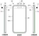
图1A、图1B和图1C是例示根据本公开的方面的示例显示装置的平面图。1A , 1B and 1C are plan views illustrating example display devices according to aspects of the present disclosure.
参考图1A、图1B和图1C,根据本公开的方面的显示装置100可以包括用于显示图像的显示面板110以及一个或更多个光学电子装置(11和/或12)。本文中,光学电子装置可被称为光检测器、光接收器或光感测装置。光学电子装置可以包括用于检测图像的相机、相机透镜、传感器、传感器等中的一个或更多个。Referring to FIGS. 1A , 1B, and 1C, a
显示面板110可以包括显示图像的显示区域DA和不显示图像的非显示区域NDA。The
多个像素可以被设置在显示区域DA中,并且用于驱动多个像素的多种类型的信号线可以被设置在其中。A plurality of pixels may be disposed in the display area DA, and various types of signal lines for driving the plurality of pixels may be disposed therein.
非显示区域NDA可以指显示区域DA之外的区域。多种类型的信号线可以被设置在非显示区域NDA中,并且多种类型的驱动电路可以连接到非显示区域NDA。非显示区域NDA的至少一部分可以被弯曲以从显示面板的前部是不可见的,或者可以被显示面板110或显示装置100的壳体(未示出)覆盖。非显示区域NDA也可以被称为边框或边框区域。The non-display area NDA may refer to an area other than the display area DA. Various types of signal lines may be provided in the non-display area NDA, and various types of driving circuits may be connected to the non-display area NDA. At least a portion of the non-display area NDA may be bent to be invisible from the front of the display panel, or may be covered by the
参考图1A、图1B和图1C,在根据本公开的方面的显示装置100中,一个或更多个光学电子装置(11和/或12)可以位于显示面板110的下方或下部(与显示面板110的观看表面相反的一侧)。Referring to FIG. 1A, FIG. 1B and FIG. 1C, in a
光可以进入显示面板110的前表面(观看表面),穿过显示面板110,到达位于显示面板110下方或位于显示面板110的下部(观看表面的相反侧)的一个或更多个光学电子装置(11和/或12)。Light can enter the front surface (viewing surface) of
一个或更多个光学电子装置(11和/或12)可以接收或检测透射通过显示面板110的光并且基于接收到的光执行预定义的功能。例如,一个或更多个光学电子装置(11和/或12)可以包括以下中的一个或更多个:图像捕获装置,诸如,相机(图像传感器)等;或传感器,诸如,接近传感器、照度传感器等。The one or more optoelectronic devices (11 and/or 12) may receive or detect light transmitted through the
参考图1A、图1B和图1C,在根据本公开的方面的显示面板110中,显示区域DA可以包括一个或更多个光学区域(OA1和/或OA2)和普通区域NA。这里,术语“普通区域”NA是当存在于显示区域DA中时不与一个或更多个光学电子装置(11和/或12)交叠的区域,并且也可以被称为非光学区域。Referring to FIGS. 1A , 1B, and 1C, in the
参考图1A、图1B和图1C,一个或更多个光学区域(OA1和/或OA2)可以是与一个或更多个光学电子装置(11和/或12)交叠的一个或更多个区域。1A, FIG. 1B and FIG. 1C, one or more optical areas (OA1 and/or OA2) may be one or more overlapping with one or more optoelectronic devices (11 and/or 12) area.
根据图1A的示例,显示区域DA可以包括第一光学区域OA1和普通区域NA。在此示例中,第一光学区域OA1的至少一部分可以与第一光学电子装置11交叠。According to the example of FIG. 1A , the display area DA may include the first optical area OA1 and the normal area NA. In this example, at least a portion of the first optical area OA1 may overlap the first
根据图1B的示例,显示区域DA可以包括光学区域OA和普通区域NA。例如,光学区域OA可以包括第一光学区域OA1和第二光学区域OA2。普通区域NA可以存在于第一光学区域OA1与第二光学区域OA2之间。在此示例中,第一光学区域OA1的至少一部分可以与第一光学电子装置11交叠,而第二光学区域OA2的至少一部分可以与第二光学电子装置12交叠。According to the example of FIG. 1B , the display area DA may include an optical area OA and a normal area NA. For example, optical area OA may include a first optical area OA1 and a second optical area OA2. A normal area NA may exist between the first optical area OA1 and the second optical area OA2. In this example, at least a portion of the first optical area OA1 may overlap the first
根据图1C的示例,显示区域DA可以包括第一光学区域OA1、第二光学区域OA2和普通区域NA。在图1C的示例中,在第一光学区域OA1和第二光学区域OA2之间可能不存在普通区域NA。例如,第一光学区域OA1和第二光学区域OA2可以彼此接触(例如,彼此直接接触)。在此示例中,第一光学区域OA1的至少一部分可以与第一光学电子装置11交叠,而第二光学区域OA2的至少一部分可以与第二光学电子装置12交叠。According to the example of FIG. 1C, the display area DA may include a first optical area OA1, a second optical area OA2, and a normal area NA. In the example of FIG. 1C, there may not be a normal area NA between the first optical area OA1 and the second optical area OA2. For example, the first optical area OA1 and the second optical area OA2 may contact each other (eg, directly contact each other). In this example, at least a portion of the first optical area OA1 may overlap the first
在一些实施方式中,期望在一个或更多个光学区域(OA1和/或OA2)中形成图像显示结构和透光结构。例如,由于一个或更多个光学区域(OA1和/或OA2)是显示区域DA的一部分,因此需要用于显示图像的像素被设置在一个或更多个光学区域(OA1和/或OA2)中。此外,为了使光能够透射一个或更多个光学电子装置(11和/或12),需要透光结构,并且因此透光结构被形成在一个或更多个光学区域(OA1和/或OA2)中。In some embodiments, it is desirable to form image display structures and light transmissive structures in one or more optical areas (OA1 and/or OA2). For example, since one or more optical areas (OA1 and/or OA2) are part of the display area DA, pixels required to display an image are disposed in one or more optical areas (OA1 and/or OA2) . In addition, in order to enable light to transmit one or more optoelectronic devices (11 and/or 12), a light-transmitting structure is required, and thus the light-transmitting structure is formed in one or more optical areas (OA1 and/or OA2) middle.
即使需要一个或更多个光学电子装置(11和/或12)来接收或检测光,一个或更多个光学电子装置(11和/或12)也可以位于显示面板110的背面上(例如,在观看表面的相反侧上)。在该实施方式中,一个或更多个光学电子装置(11和/或12)位于(例如)显示面板110下方或位于显示面板110的下部中,并且被配置为接收已透射显示面板110的光。Even if one or more optoelectronic devices (11 and/or 12) are required to receive or detect light, one or more optoelectronic devices (11 and/or 12) may be located on the back of the display panel 110 (e.g., on the opposite side of the viewing surface). In this embodiment, one or more optoelectronic devices (11 and/or 12) are located, for example, below or in a lower portion of the
例如,一个或更多个光学电子装置(11和/或12)未暴露于显示面板110的前表面(观看表面)中。因此,当用户面对显示装置100的前表面时,一个或更多个光学电子装置(11和/或12)被设置成使得它们对用户来说是不可见的。For example, one or more optoelectronic devices ( 11 and/or 12 ) are not exposed in the front surface (viewing surface) of the
在一个实施方式中,第一光学电子装置11可以是相机,并且第二光学电子装置12可以是诸如接近传感器、照度传感器、红外传感器等的传感器。例如,相机可以是相机镜头、图像传感器或包括相机镜头和图像传感器中的至少一个的单元。传感器可以是例如能够检测红外射线的红外传感器。In one embodiment, the first
在另一实施方式中,第一光学电子装置11可以是传感器,而第二光学电子装置12可以是相机。In another embodiment, the first
在下文中,为了方便起见,下面的讨论将参考第一光学电子装置11是相机而第二光学电子装置12是传感器的实施方式。然而,应当理解,本公开的范围包括第一光学电子装置11是传感器而第二光学电子装置12是相机的实施方式。例如,相机可以是相机镜头、图像传感器或包括相机镜头和图像传感器中的至少一个的单元。In the following, for convenience, the following discussion will refer to an embodiment in which the first
在第一光学电子装置11是相机的示例中,该相机可以位于显示面板110的背面(例如,在显示面板110下方或下部),并且为能够在显示面板110的前方方向上捕获对象或图像的前置相机。因此,用户可以在观看显示面板110的观看表面的同时通过相机捕获在观看表面上不可见的图像或对象。In an example where the first
第一光学电子装置11可以通过显示装置产生关于观看图像的用户的用户信息。由第一光学电子装置11获得的用户信息可以是例如通过捕获用户而获得的图像。通过捕获用户而获得的图像可以包括关于用户的面部的信息。第一光学电子装置11可以获得通过连续捕获图像而获得的静止图像或视频图像。The first optical
尽管图1A、图1B和图1C中的每一者中的显示区域DA中包括的普通区域NA和一个或更多个光学区域(OA1和/或OA2)是可以显示图像的区域,但是普通区域NA是不需要形成光透射结构的区域,但是一个或更多个光学区域(OA1和/或OA2)是需要形成光透射结构的区域。因此,在一些实施方式中,普通区域NA是未实现或未包括光透射结构的区域,并且一个或更多个光学区域(OA1和/或OA2)是实现或包括光透射结构的区域。Although the normal area NA and one or more optical areas (OA1 and/or OA2) included in the display area DA in each of FIGS. 1A, 1B, and 1C are areas where images can be displayed, the normal area NA is an area where light-transmissive structures do not need to be formed, but one or more optical areas (OA1 and/or OA2) are areas where light-transmissive structures need to be formed. Thus, in some embodiments, the normal area NA is an area where no light-transmissive structures are implemented or included, and one or more optical areas (OA1 and/or OA2) are areas where light-transmissive structures are implemented or included.
因此,一个或更多个光学区域(OA1和/或OA2)可以具有大于或等于预定水平的透射率(即,相对高的透射率),并且普通区域NA可以不具有透光率或具有小于预定水平的透射率(即,相对低的透射率)。Accordingly, one or more optical areas (OA1 and/or OA2) may have a transmittance greater than or equal to a predetermined level (ie, relatively high transmittance), and the normal area NA may have no transmittance or have a transmittance less than a predetermined level. Horizontal transmittance (ie, relatively low transmittance).
例如,一个或更多个光学区域(OA1和/或OA2)可以具有与普通区域NA不同的分辨率、像素设置结构、每单位面积的像素数量、电极结构、线结构、电极设置结构、线设置结构等。For example, one or more optical areas (OA1 and/or OA2) may have a different resolution, pixel arrangement, number of pixels per unit area, electrode structure, line structure, electrode arrangement structure, line arrangement than the normal area NA. structure etc.
在实施方式中,一个或更多个光学区域(OA1和/或OA2)中每单位面积的像素数量可以小于普通区域NA中每单位面积的像素数量。例如,一个或更多个光学区域(OA1和/或OA2)的分辨率可以低于普通区域NA的分辨率。这里,每单位面积的像素数量可以用作测量分辨率的单位,并且使用表示1英寸内的像素数量的每英寸像素(PPI)来测量。In an embodiment, the number of pixels per unit area in one or more optical areas (OA1 and/or OA2) may be smaller than the number of pixels per unit area in the normal area NA. For example, the resolution of one or more optical areas (OA1 and/or OA2) may be lower than the resolution of the normal area NA. Here, the number of pixels per unit area may be used as a unit for measuring resolution, and is measured using pixels per inch (PPI) representing the number of pixels within 1 inch.
在实施方式中,在图1A至图1C中的每一者中,第一光学区域OA1中的每单位面积的像素数量可以小于普通区域NA中的每单位面积的像素数量。在实施方式中,在图1B和图1C中的每一者中,第二光学区域OA2中的每单位面积的像素数量可以大于或等于第一光学区域OA1中的每单位面积的像素数量。In an embodiment, in each of FIGS. 1A to 1C , the number of pixels per unit area in the first optical area OA1 may be smaller than the number of pixels per unit area in the normal area NA. In an embodiment, in each of FIGS. 1B and 1C , the number of pixels per unit area in the second optical area OA2 may be greater than or equal to the number of pixels per unit area in the first optical area OA1 .
在图1A、图1B和图1C中的每一者中,第一光学区域OA1可以具有各种形状,诸如,圆形、椭圆形、四边形、六边形、八边形等。在图1B和图1C的每一者中,第二光学区域OA2可以具有各种形状,诸如,圆形、椭圆形、四边形、六边形、八边形等。第一光学区域OA1和第二光学区域OA2可以具有相同的形状或不同的形状。In each of FIGS. 1A , 1B, and 1C, the first optical area OA1 may have various shapes, such as a circle, an ellipse, a quadrangle, a hexagon, an octagon, and the like. In each of FIGS. 1B and 1C , the second optical area OA2 may have various shapes, such as a circle, an ellipse, a quadrangle, a hexagon, an octagon, and the like. The first optical area OA1 and the second optical area OA2 may have the same shape or different shapes.
在一些实施方式中,作为用于增加第一光学区域OA1和第二光学区域OA2中的至少一个的透射率的方法,可以应用一种技术(其可以被称为“像素密度差异设计方案”),使得可以如上所述区分像素(或子像素)的密度或像素(或子像素)的集成程度。根据像素密度差异设计方案,在实施方式中,显示面板110可以被配置为或设计成使得第一光学区域OA1和第二光学区域OA2中的至少一者的每单位面积的像素(或子像素)数量大于普通区域NA的每单位面积的像素(或子像素)数量。In some embodiments, as a method for increasing the transmittance of at least one of the first optical area OA1 and the second optical area OA2, a technique (which may be referred to as "pixel density difference design scheme") may be applied , so that the density of pixels (or sub-pixels) or the degree of integration of pixels (or sub-pixels) can be distinguished as described above. According to the pixel density difference design scheme, in an embodiment, the
在另一实施方式中,作为用于增加第一光学区域OA1和第二光学区域OA2中的至少一者的透射率的另一方法,可以应用另一技术(其可被称作“像素尺寸差异设计方案”),使得可以区分像素(或子像素)的尺寸。根据像素尺寸差异设计方案,显示面板110可以被配置为或设计成使得第一光学区域OA1和第二光学区域OA2中的至少一者的每单位面积的像素(或子像素)数量等于或类似于普通区域NA的每单位面积的像素(或子像素)数量;然而,设置在第一光学区域OA1和第二光学区域OA2中的至少一者中的每一像素(或子像素)的尺寸(即,对应发光区域的尺寸)小于设置在普通区域NA中的每一像素(或子像素)的尺寸(即,对应发光区域的尺寸)。In another embodiment, as another method for increasing the transmittance of at least one of the first optical area OA1 and the second optical area OA2, another technique (which may be referred to as "pixel size difference") may be applied. design scheme"), making it possible to distinguish the size of a pixel (or sub-pixel). According to the pixel size difference design scheme, the
参考图1C,在第一光学区域OA1和第二光学区域OA2彼此接触的示例中,包括第一光学区域OA1和第二光学区域OA2的整个光学区域也可以具有各种形状,诸如圆形、椭圆形、四边形、六边形、八边形等。Referring to FIG. 1C, in an example where the first optical area OA1 and the second optical area OA2 are in contact with each other, the entire optical area including the first optical area OA1 and the second optical area OA2 may also have various shapes, such as a circle, an ellipse Shapes, quadrilaterals, hexagons, octagons, etc.
在下文中,为了便于描述,将基于第一光学区域OA1和第二光学区域OA2中的每一者具有圆形形状的实施方式来提供讨论。然而,应理解,本公开的范围包括第一光学区域OA1和第二光学区域OA2中的一者或两者具有不同于圆形形状的形状的实施方式。Hereinafter, for convenience of description, a discussion will be provided based on an embodiment in which each of the first optical area OA1 and the second optical area OA2 has a circular shape. However, it should be understood that the scope of the present disclosure includes embodiments in which one or both of the first optical area OA1 and the second optical area OA2 has a shape other than a circular shape.
在根据本公开的方面的显示装置100具有第一光学电子装置11(例如,相机)等位于显示面板110的下方或位于显示面板110的下部中而不暴露于外部的结构的示例中,根据本公开的方面的显示装置100可以被称为实现屏下摄像头(UDC)技术的显示器。In an example in which the
根据这些示例,根据本公开的方面的显示装置100可以具有防止显示区域DA的尺寸减小的优点,因为不需要在显示面板110中形成用于暴露相机的凹口或相机孔。According to these examples, the
由于不需要在显示面板110中形成用于相机暴露的凹口或相机孔,因此显示装置100可以具有减小边框区域的尺寸并且改进设计自由度的进一步优点,因为移除了设计的这种限制。Since there is no need to form a notch or a camera hole for camera exposure in the
尽管一个或更多个光学电子装置(11和/或12)位于显示装置100的显示面板110的背面(例如,在显示面板110的下方或下部中)(例如,隐藏或不暴露于外部),但是需要一个或更多个光学电子装置(11和/或12)来执行正常的预定义功能,并且因此接收或检测光。Although one or more optoelectronic devices (11 and/or 12) are located on the back side of the
此外,在根据本公开的方面的显示装置100中,尽管一个或更多个光学电子装置(11和/或12)位于显示面板110的背面(例如,在显示面板110的下方或下部中)以被隐藏和设置为与显示区域DA交叠,但是图像显示通常在显示区域DA中的与一个或更多个光学电子装置(11和/或12)交叠的一个或更多个光学区域(OA1和/或OA2)中执行。因此,在一个或更多个示例中,即使一个或更多个光学电子装置(11和/或12)位于显示面板的背面,图像也可以在显示区域DA中的与一个或更多个光学电子装置(11和/或12)交叠的一个或更多个光学区域(OA1和/或OA2)中以正常方式(例如,不降低图像质量)显示。In addition, in the
图2示出了根据本公开的方面的显示装置100的示例系统构造。FIG. 2 illustrates an example system configuration of the
参考图2,显示装置100可以包括显示面板110和显示驱动电路作为用于显示图像的组件。Referring to FIG. 2 , the
显示驱动电路是用于驱动显示面板110的电路,并且可以包括数据驱动电路220、选通驱动电路230、显示控制器240和其他组件。The display driving circuit is a circuit for driving the
显示面板110可以包括显示图像的显示区域DA和不显示图像的非显示区域NDA。非显示区域NDA可以是显示区域DA之外的区域,并且也可以被称为边缘区域或边框区域。非显示区域NDA的全部或一部分可以是从显示装置100的前表面可见的区域,或者是从显示装置100的前表面弯曲并不可见的区域。The
显示面板110可以包括基板SUB以及设置在基板SUB上的多个像素SP。显示面板110还可以包括各种类型的信号线以驱动多个像素SP。所述多个像素SP中的每一者可以例如包括发射红光的红色子像素、发射绿光的绿色子像素以及发射蓝光的蓝色子像素。此外,一个像素可以表现对应于红色子像素、绿色子像素和蓝色子像素的相应亮度的颜色。The
在一个实施方式中,根据本公开的方面的显示装置100可以是液晶显示装置。在另一示例中,根据本公开的方面的显示装置100可以为其设置在其显示面板110中的像素自身发射光的自发射显示装置。在根据本公开的方面的显示装置100是自发射显示装置的示例中,多个像素SP中的每一者可以包括发光元件。In one embodiment, the
在一个实施方式中,根据本公开的方面的显示装置100可以为使用有机发光二极管(OLED)实现发光元件的有机发光显示装置。在另一实施方式中,根据本公开的方面的显示装置100可以为使用基于无机材料的发光二极管实现发光元件的无机发光显示装置。在另一实施方式中,根据本公开的方面的显示装置100可以是使用量子点实现发光元件的量子点显示装置,所述量子点是自发射半导体晶体。In one embodiment, the
多个像素SP中的每一者的结构可以根据显示装置100的类型而变化。在显示装置100是包括自发射像素SP的自发射显示装置的示例中,每个像素SP可以包括自发射发光元件、一个或更多个晶体管和一个或更多个电容器。The structure of each of the plurality of pixels SP may vary according to the type of the
设置在显示装置100中的各种类型的信号线可以包括例如用于承载数据信号(其可以被称为数据电压或图像信号)的多条数据线DL、用于承载选通信号(其可以被称为扫描信号)的多条选通线GL等。Various types of signal lines provided in the
多条数据线DL和多条选通线GL可以彼此相交。多条数据线DL中的每一者可以在第一方向上延伸。多条选通线GL中的每一者可以在第二方向上延伸。A plurality of data lines DL and a plurality of gate lines GL may cross each other. Each of the plurality of data lines DL may extend in the first direction. Each of the plurality of gate lines GL may extend in the second direction.
例如,第一方向可以是列或垂直方向,并且第二方向可以是行或水平方向。在另一示例中,第一方向可以是行方向,并且第二方向可以是列方向。For example, the first direction may be a column or vertical direction, and the second direction may be a row or horizontal direction. In another example, the first direction may be a row direction, and the second direction may be a column direction.
数据驱动电路220是用于驱动多条数据线DL的电路,并且可以向多条数据线DL供应数据信号。选通驱动电路230是用于驱动多条选通线GL的电路,并且可以向多条选通线GL提供选通信号。The
显示控制器240可以是用于控制数据驱动电路220和选通驱动电路230的装置,并且可以控制多条数据线DL的驱动定时和多条选通线GL的驱动定时。The
显示控制器240可以向数据驱动电路220提供数据驱动控制信号DCS以控制数据驱动电路220,并向选通驱动电路230提供选通驱动控制信号GCS以控制选通驱动电路230。The
显示控制器240可以从主机系统250接收输入图像数据,并且基于输入图像数据将图像数据Data供应到数据驱动电路220。The
数据驱动电路220可以根据显示控制器240的驱动定时控制向多条数据线DL供应数据信号。The
数据驱动电路220可以从显示控制器240接收数字图像数据Data,将接收到的图像数据Data转换为模拟数据信号,并将得到的模拟数据信号提供给多条数据线DL。The
选通驱动电路230可以根据显示控制器240的定时控制向多条选通线GL提供选通信号。选通驱动电路230可以接收对应于接通电平电压的第一选通电压和对应于关断电平电压的第二选通电压以及各种选通驱动控制信号GCS,生成选通信号,并且将生成的选通信号供应到多条选通线GL。The
在一些实施方式中,数据驱动电路220可以以卷带式自动接合(TAB)型连接到显示面板110,或以玻璃上芯片(COG)型或面板上芯片(COP)型连接到导电焊盘(诸如,显示面板110的接合焊盘),或以薄膜上芯片(COF)型连接到显示面板110。In some embodiments, the
在一些实施方式中,选通驱动电路230可以以卷带式自动接合(TAB)型连接到显示面板110,或以玻璃上芯片(COG)型或面板上芯片(COP)型连接到导电焊盘(诸如,显示面板110的接合焊盘),或以薄膜上芯片(COF)型连接到显示面板110。在另一实施方式中,选通驱动电路230可以以面板中栅极(GIP)型被设置在显示面板110的非显示区域NDA中。选通驱动电路230可以被设置在基板上或基板上方,或者连接到基板。也就是说,在GIP类型的情况下,选通驱动电路230可以被设置在基板的非显示区域NDA中。选通驱动电路230可以在玻璃上芯片(COG)型、薄膜上芯片(COF)型等的情况下连接至基板。In some embodiments, the
在一些实施方式中,数据驱动电路220和选通驱动电路230中的至少一者可以被设置在显示面板110的显示区域DA中。例如,数据驱动电路220和选通驱动电路230中的至少一者可以被设置为不与像素SP交叠,或者被设置为与像素SP中的一个或更多个或全部交叠。In some embodiments, at least one of the
数据驱动电路220也可以位于(但不限于)显示面板110的仅一侧或部分(例如,上边缘或下边缘)上。在一些实施方式中,数据驱动电路220可以根据驱动方案、面板设计方案等位于但不限于显示面板110的两侧或部分(例如,上边缘和下边缘)或显示面板110的四个侧面或部分(例如,上边缘、下边缘、左边缘和右边缘)中的至少两个。The
选通驱动电路230可以仅位于显示面板110的一侧或部分(例如,左边缘或右边缘)中。在一些实施方式中,选通驱动电路230可以连接到面板110的两侧或部分(例如,左边缘和右边缘),或者根据驱动方案、面板设计方案等连接到面板110的四侧或部分(例如,上边缘、下边缘、左边缘和右边缘)中的至少两个。The
显示控制器240可以以与数据驱动电路220分离的组件实现,或者与数据驱动电路220集成,并且因此以集成电路实现。The
显示控制器240可以是在典型显示技术中使用的定时控制器,或者是能够执行除了典型定时控制器的功能之外的其他控制功能的控制器或控制装置。在一些实施方式中,显示控制器140可以是与定时控制器不同的控制器或控制装置,或者是包括在控制器或控制装置中的电路或组件。显示控制器240可以用各种电路或电子组件(诸如,集成电路(IC)、现场可编程门阵列(FPGA)、专用集成电路(ASIC)、处理器等)来实现。在一些实施方式中,显示控制器240可以是应用处理器(AP)。The
显示控制器240可以被安装在印刷电路板、柔性印刷电路等上,并且通过印刷电路板、柔性印刷电路等电连接至选通驱动电路230和数据驱动电路220。The
显示控制器240可以经由一个或更多个预定义的接口向数据驱动电路220发送信号和从数据驱动电路220接收信号。在一些实施方式中,这样的接口可以包括低电压差分信令(LVDS)接口、嵌入式时钟点-点接口(EPI)、串行外围接口(SPI)等。The
在一些实施方式中,为了进一步提供触摸感测功能以及图像显示功能,显示装置100可以包括至少一个触摸传感器和触摸感测电路,该触摸感测电路能够通过感测触摸传感器来检测触摸事件是否通过触摸对象(诸如,手指、笔等)发生,或者检测对应的触摸位置。In some implementations, in order to further provide a touch sensing function and an image display function, the
触摸感测电路可以包括能够通过驱动和感测触摸传感器来生成和提供触摸感测数据的触摸驱动电路260、能够检测触摸事件的发生或使用触摸感测数据检测触摸位置的触摸控制器270以及一个或更多个其他组件。The touch sensing circuit may include a
触摸传感器可以包括多个触摸电极。触摸传感器还可以包括用于将多个触摸电极电连接到触摸驱动电路260的多条触摸线。A touch sensor may include a plurality of touch electrodes. The touch sensor may also include a plurality of touch lines for electrically connecting the plurality of touch electrodes to the
触摸传感器可以在显示面板110外部以触摸面板或以触摸面板的形式实现,或在显示面板110内部实现。在触摸传感器在显示面板110的外部以触摸面板或者以触摸面板的形式实现的示例中,这样的触摸传感器被称为附加类型。在设置附加类型的触摸传感器的示例中,触摸面板和显示面板110可以在组装过程期间单独地制造和联接。附加类型的触摸面板可以包括触摸面板基板和触摸面板基板上的多个触摸电极。The touch sensor may be implemented in or in the form of a touch panel outside the
在触摸传感器在显示面板110内实现的示例中,制造显示面板110的工艺可以包括将触摸传感器和与驱动显示装置100相关的信号线和电极一起设置在基板SUB上方。In an example where the touch sensor is implemented in the
触摸驱动电路260可以向多个触摸电极中的至少一个供应触摸驱动信号,并且感测多个触摸电极中的至少一个以产生触摸感测数据。The
触摸感测电路可以使用自电容感测技术或互电容感测技术来执行触摸感测。The touch sensing circuit may perform touch sensing using self-capacitance sensing technology or mutual capacitance sensing technology.
在触摸感测电路以自电容感测技术执行触摸感测的示例中,触摸感测电路可以基于每个触摸电极与触摸对象(例如,手指、笔等)之间的电容来执行触摸感测。In an example where the touch sensing circuit performs touch sensing with a self-capacitance sensing technique, the touch sensing circuit may perform touch sensing based on capacitance between each touch electrode and a touching object (eg, finger, pen, etc.).
根据自电容感测方法,多个触摸电极中的每一者可以用作驱动触摸电极和感测触摸电极两者。触摸驱动电路260可以驱动多个触摸电极中的全部或一个或更多个,并且感测多个触摸电极中的全部或一个或更多个。According to the self-capacitance sensing method, each of the plurality of touch electrodes can function as both a driving touch electrode and a sensing touch electrode. The
在触摸感测电路以互电容感测技术执行触摸感测的示例中,触摸感测电路可以基于触摸电极之间的电容来执行触摸感测。In examples where the touch sensing circuit performs touch sensing with a mutual capacitance sensing technique, the touch sensing circuit may perform touch sensing based on capacitance between touch electrodes.
根据互电容感测方法,所述多个触摸电极被划分为驱动触摸电极和感测触摸电极。触摸驱动电路260可以驱动驱动触摸电极并感测感测触摸电极。According to the mutual capacitance sensing method, the plurality of touch electrodes are divided into driving touch electrodes and sensing touch electrodes. The
触摸感测电路中包括的触摸驱动电路260和触摸控制器270可以在分开的装置中或单个装置中实现。此外,触摸驱动电路260和数据驱动电路220可以在分开的装置中或在单个装置中实现。The
显示装置100还可以包括用于向显示驱动电路和/或触摸感测电路供应各种类型的电力的电源电路。The
在一些实施方式中,显示装置100可以是诸如智能电话、平板电脑等的移动终端,或者监视器、电视(TV)等。此类装置可以具有各种类型、尺寸和形状。根据本公开的实施方式的显示装置100不限于此,并且包括用于显示信息或图像的各种类型、尺寸和形状的显示器。In some embodiments, the
如上所述,显示面板110的显示区域DA可以包括普通区域NA和一个或更多个光学区域(OA1和/或OA2),例如,如图1A、图1B和图1C所示。As described above, the display area DA of the
普通区域NA和一个或更多个光学区域(OA1和/或OA2)是可以显示图像的区域。然而,正常NA是不需要实现光透射结构的区域,并且一个或更多个光学区域(OA1和/或OA2)是需要实现光透射结构的区域。The normal area NA and one or more optical areas (OA1 and/or OA2) are areas where images can be displayed. However, the normal NA is an area where light-transmissive structures do not need to be implemented, and one or more optical areas (OA1 and/or OA2) are areas where light-transmissive structures need to be implemented.
如以上关于图1A、图1B和图1C的示例所讨论的,尽管为了便于描述,除了普通区域NA之外,显示面板110的显示区域DA还可以包括一个或更多个光学区域(OA1和/或OA2),但是在随后的讨论中,假设显示区域DA包括第一光学区域(OA1)和第二光学区域(OA2)以及普通区域NA;并且其普通区域NA包括图1A至图1C中的普通区域NA,并且其第一光学区域(OA1)和第二光学区域(OA2)分别包括图1A、图1B和图1C中的第一光学区域OA1以及图1B和图1C的第二光学区域OA2,除非另有明确说明。As discussed above with respect to the examples of FIGS. 1A , 1B, and 1C, although for convenience of description, the display area DA of the
图3示出了根据本公开的方面的显示面板110中的子像素SP的示例等效电路。FIG. 3 illustrates an example equivalent circuit of a subpixel SP in the
设置在显示面板110的显示区域DA中的普通区域NA、第一光学区域OA1和第二光学区域OA2中的子像素SP中的每一者可以包括发光元件ED、用于驱动发光元件ED的驱动晶体管DRT、用于将数据电压Vdata传送到驱动晶体管DRT的第一节点N1的扫描晶体管SCT、用于在一个帧期间将电压维持在近似恒定电平的存储电容器Cst等。Each of the normal area NA, the first optical area OA1, and the sub-pixel SP in the second optical area OA2 disposed in the display area DA of the
驱动晶体管DRT可以包括施加数据电压的第一节点N1、电连接到发光元件ED的第二节点N2和通过驱动电压线DVL施加像素驱动电压ELVDD的第三节点N3。在驱动晶体管DRT中,第一节点N1可以是栅极节点,第二节点N2可以是源极节点或漏极节点,并且第三节点N3可以是漏极节点或源极节点。The driving transistor DRT may include a first node N1 to which a data voltage is applied, a second node N2 electrically connected to the light emitting element ED, and a third node N3 to which a pixel driving voltage ELVDD is applied through a driving voltage line DVL. In the driving transistor DRT, the first node N1 may be a gate node, the second node N2 may be a source node or a drain node, and the third node N3 may be a drain node or a source node.
发光元件ED可以包括阳极AE、发光层EL和阴极CE。阳极AE可以是设置在每个像素(或子像素)SP中的像素电极,并且可以电连接到每个子像素SP的驱动晶体管DRT的第二节点N2。阴极CE可以是通常设置在多个子像素SP中的公共电极,并且诸如低电平电压的基础电压ELVSS可以被施加到阴极CE。The light emitting element ED may include an anode AE, a light emitting layer EL and a cathode CE. The anode AE may be a pixel electrode provided in each pixel (or sub-pixel) SP, and may be electrically connected to the second node N2 of the driving transistor DRT of each sub-pixel SP. The cathode CE may be a common electrode generally provided in a plurality of sub-pixels SP, and a base voltage ELVSS such as a low level voltage may be applied to the cathode CE.
例如,阳极AE可以是像素电极,并且阴极CE可以是公共电极。在另一示例中,阳极AE可以是公共电极,并且阴极CE可以是像素电极。为了便于描述,在随后的讨论中,假设阳极AE是像素电极,并且阴极CE是公共电极,除非另有明确说明。For example, the anode AE may be a pixel electrode, and the cathode CE may be a common electrode. In another example, the anode AE may be a common electrode, and the cathode CE may be a pixel electrode. For ease of description, in the ensuing discussion, it is assumed that the anode AE is the pixel electrode, and the cathode CE is the common electrode, unless explicitly stated otherwise.
发光元件ED可以是例如有机发光二极管(OLED)、无机发光二极管、量子点发光元件等。在有机发光二极管用作发光元件ED的示例中,包括在发光元件ED中的发光层EL可以包括包含有机材料的有机发光层。The light emitting element ED may be, for example, an organic light emitting diode (OLED), an inorganic light emitting diode, a quantum dot light emitting element, or the like. In an example where an organic light emitting diode is used as the light emitting element ED, the light emitting layer EL included in the light emitting element ED may include an organic light emitting layer including an organic material.
扫描晶体管SCT可以通过扫描信号SCAN导通和截止,所述扫描信号SCAN为通过选通线GL施加的选通信号,并且电连接在驱动晶体管DRT的第一节点N1与数据线DL之间。The scan transistor SCT may be turned on and off by a scan signal SCAN, which is a gate signal applied through a gate line GL and electrically connected between the first node N1 of the driving transistor DRT and the data line DL.
存储电容器Cst可以电连接在驱动晶体管DRT的第一节点N1与第二节点N2之间。The storage capacitor Cst may be electrically connected between the first node N1 and the second node N2 of the driving transistor DRT.
每一子像素SP可以包括两个晶体管(2T:DRT和SCT)以及一个电容器(1C:Cst)(其可称为“2T1C结构”),如图3中所说明,并且在一些情况下,还可以包括一个或更多个晶体管,或还可以包括一个或更多个电容器。Each subpixel SP may include two transistors (2T: DRT and SCT) and a capacitor (1C: Cst) (which may be referred to as a "2T1C structure"), as illustrated in FIG. 3 , and in some cases, also One or more transistors may be included, or one or more capacitors may also be included.
在一些实施方式中,可存在于驱动晶体管DRT的第一节点N1与第二节点N2之间的存储电容器Cst可以为被有意配置或设计成位于驱动晶体管DRT外部的外部电容器,而非内部电容器(例如,寄生电容器(例如,栅极到源极电容Cgs、栅极到漏极电容Cgd等))。In some embodiments, the storage capacitor Cst that may exist between the first node N1 and the second node N2 of the driving transistor DRT may be an external capacitor that is intentionally configured or designed to be located outside the driving transistor DRT instead of an internal capacitor ( For example, parasitic capacitors (eg, gate-to-source capacitance Cgs, gate-to-drain capacitance Cgd, etc.)).
驱动晶体管DRT和扫描晶体管SCT中的每一者可以是n型晶体管或p型晶体管。Each of the driving transistor DRT and the scanning transistor SCT may be an n-type transistor or a p-type transistor.
由于每个子像素SP中的电路元件(例如,特别是发光元件ED)易受外部水分或氧气的影响,因此封装层ENCAP可以被设置在显示面板110中,以防止外部水分或氧气穿透到电路元件(例如,特别是发光元件ED)中。封装层ENCAP可以被设置为覆盖发光元件ED。Since the circuit elements (for example, especially the light emitting element ED) in each sub-pixel SP are susceptible to external moisture or oxygen, the encapsulation layer ENCAP may be provided in the
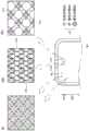
图4示出了根据本公开的方面的包括在显示面板110的显示区域DA中的三个区域(NA、OA1和OA2)中的像素SP的示例设置。4 illustrates an example arrangement of pixels SP included in three areas (NA, OA1, and OA2) in the display area DA of the
参考图4,在一些实施方式中,多个像素SP可以被设置在显示区域DA中包括的普通区域NA、第一光学区域OA1和第二光学区域OA2中的每一者中。Referring to FIG. 4 , in some embodiments, a plurality of pixels SP may be disposed in each of the normal area NA, the first optical area OA1 , and the second optical area OA2 included in the display area DA.
所述多个像素SP中的每一者可以包括(例如)发射红光的红色子像素(红色SP)、发射绿光的绿色子像素(绿色SP)和发射蓝光的蓝色子像素(蓝色SP)。Each of the plurality of pixels SP may include, for example, a red sub-pixel (red SP) emitting red light, a green sub-pixel (green SP) emitting green light, and a blue sub-pixel (blue SP) emitting blue light. SP).
因此,普通区域NA、第一光学区域OA1和第二光学区域OA2中的每一者可以包括一个或更多个红色子像素(红色SP)的一个或更多个发光区域EA,以及一个或更多个绿色子像素(绿色SP)的一个或更多个发光区域EA,以及一个或更多个蓝色子像素(蓝色SP)的一个或更多个发光区域EA。Accordingly, each of the normal area NA, the first optical area OA1, and the second optical area OA2 may include one or more light emitting areas EA of one or more red sub-pixels (red SP), and one or more One or more light emitting areas EA of a plurality of green sub-pixels (green SP), and one or more light emitting areas EA of one or more blue sub-pixels (blue SP).
参考图4,在一些实施方式中,普通区域NA可以不包括光透射结构,但是可以包括发光区域EA。Referring to FIG. 4 , in some embodiments, the normal area NA may not include the light transmissive structure, but may include the light emitting area EA.
相反,在一些实施方式中,第一光学区域OA1和第二光学区域OA2需要包括发光区域EA和光透射结构。On the contrary, in some embodiments, the first optical area OA1 and the second optical area OA2 need to include the light emitting area EA and the light transmissive structure.
因此,第一光学区域OA1可以包括一个或更多个发光区域EA和一个或更多个第一透射区域TA1,并且第二光学区域OA2可以包括一个或更多个发光区域EA和一个或更多个第二透射区域TA2。Accordingly, the first optical area OA1 may include one or more light emitting areas EA and one or more first transmissive areas TA1, and the second optical area OA2 may include one or more light emitting areas EA and one or more A second transmission area TA2.
根据是否允许光的透射,发光区域EA和透射区域(TA1和/或TA2)可以是不同的。例如,发光区域EA可以是不允许光透射的区域(例如,不允许光透射到显示面板的背面),并且透射区域(TA1和/或TA2)可以是允许光透射的区域(例如,允许光透射到显示面板的背面)。The light emitting area EA and the transmissive area ( TA1 and/or TA2 ) may be different according to whether transmission of light is allowed. For example, the light emission area EA may be an area that does not allow light to transmit (for example, does not allow light to transmit to the back of the display panel), and the transmission area ( TA1 and/or TA2 ) may be an area that allows light to the back of the display panel).
根据是否包括特定金属层,发光区域EA和透射区域(TA1和/或TA2)也可以是不同的。例如,如图3所示的阴极CE可以被设置在发光区域EA中,并且阴极CE可以不被设置在透射区域(TA1和/或TA2)中。在一些实施方式中,光屏蔽层可以被设置在发光区域EA中,并且光屏蔽层可以不被设置在透射区域(TA1和/或TA2)中。The light emitting area EA and the transmissive area ( TA1 and/or TA2 ) may also be different depending on whether a specific metal layer is included. For example, the cathode CE as shown in FIG. 3 may be disposed in the light emitting area EA, and the cathode CE may not be disposed in the transmissive area ( TA1 and/or TA2 ). In some embodiments, the light shielding layer may be disposed in the light emitting area EA, and the light shielding layer may not be disposed in the transmissive area ( TA1 and/or TA2 ).
由于第一光学区域OA1包括第一透射区域TA1,并且第二光学区域OA2包括第二透射区域TA2,所以第一光学区域OA1和第二光学区域OA2两者都是光可以透射通过的区域。Since the first optical area OA1 includes the first transmissive area TA1 and the second optical area OA2 includes the second transmissive area TA2, both the first optical area OA1 and the second optical area OA2 are areas through which light may be transmitted.
在一个实施方式中,第一光学区域OA1的透射率(透射程度)和第二光学区域OA2的透射率(透射程度)可以基本上相等。In one embodiment, the transmittance (degree of transmission) of the first optical area OA1 and the transmittance (degree of transmission) of the second optical area OA2 may be substantially equal.
例如,第一光学区域OA1的第一透射区域TA1和第二光学区域OA2的第二透射区域TA2可以具有基本上相同的形状或尺寸。在另一示例中,即使当第一光学区域OA1的第一透射区域TA1和第二光学区域OA2的第二透射区域TA2具有不同的形状或尺寸时,第一透射区域TA1与第一光学区域OA1的比率和第二透射区域TA2与第二光学区域OA2的比率也可以基本上相等。在一个示例中,第一透射区域TA1中的每一者具有相同的形状和尺寸。在一个示例中,第二透射区域TA2中的每一者具有相同的形状和尺寸。For example, the first transmissive area TA1 of the first optical area OA1 and the second transmissive area TA2 of the second optical area OA2 may have substantially the same shape or size. In another example, even when the first transmissive area TA1 of the first optical area OA1 and the second transmissive area TA2 of the second optical area OA2 have different shapes or sizes, the first transmissive area TA1 and the first optical area OA1 The ratio of and the ratio of the second transmissive area TA2 to the second optical area OA2 may also be substantially equal. In one example, each of the first transmissive areas TA1 has the same shape and size. In one example, each of the second transmissive areas TA2 has the same shape and size.
在另一实施方式中,第一光学区域OA1的透射率(透射程度)与第二光学区域OA2的透射率(透射程度)可以不同。In another embodiment, the transmittance (degree of transmission) of the first optical area OA1 and the transmittance (degree of transmission) of the second optical area OA2 may be different.
例如,第一光学区域OA1的第一透射区域TA1和第二光学区域OA2的第二透射区域TA2可以具有不同的形状或尺寸。在另一示例中,即使当第一光学区域OA1的第一透射区域TA1和第二光学区域OA2的第二透射区域TA2具有基本上相同的形状或尺寸时,第一透射区域TA1与第一光学区域OA1的比率和第二透射区域TA2与第二光学区域OA2的比率也可以彼此不同。For example, the first transmissive area TA1 of the first optical area OA1 and the second transmissive area TA2 of the second optical area OA2 may have different shapes or sizes. In another example, even when the first transmissive area TA1 of the first optical area OA1 and the second transmissive area TA2 of the second optical area OA2 have substantially the same shape or size, the first transmissive area TA1 and the first optical area OA2 have substantially the same shape or size. The ratio of the area OA1 and the ratio of the second transmissive area TA2 to the second optical area OA2 may also be different from each other.
例如,在如图1A、图1B和图1C所示的与第一光学区域OA1交叠的第一光学电子装置11是相机并且如图1B和1C所示的与第二光学区域OA2交叠的第二光学电子装置12是用于检测图像的传感器的示例中,与传感器相比,相机可能需要更大量的光。For example, where the first
因此,第一光学区域OA1的透射率(透射程度)可以大于第二光学区域OA2的透射率(透射程度)。Accordingly, the transmittance (degree of transmission) of the first optical area OA1 may be greater than the transmittance (degree of transmission) of the second optical area OA2.
例如,第一光学区域OA1的第一透射区域TA1可以具有大于第二光学区域OA2的第二透射区域TA2的尺寸。在另一示例中,即使当第一光学区域OA1的第一透射区域TA1和第二光学区域OA2的第二透射区域TA2具有基本相同的尺寸时,第一透射区域TA1与第一光学区域OA1的比率也可以大于第二透射区域TA2与第二光学区域OA2的比率。For example, the first transmissive area TA1 of the first optical area OA1 may have a larger size than the second transmissive area TA2 of the second optical area OA2. In another example, even when the first transmissive area TA1 of the first optical area OA1 and the second transmissive area TA2 of the second optical area OA2 have substantially the same size, the first transmissive area TA1 and the first optical area OA1 The ratio may also be greater than the ratio of the second transmissive area TA2 to the second optical area OA2.
为了便于描述,基于第一光学区域OA1的透射率(透射程度)大于第二光学区域OA2的透射率(透射程度)的实施方式来提供以下讨论。For convenience of description, the following discussion is provided based on an embodiment in which the transmittance (degree of transmission) of the first optical area OA1 is greater than the transmittance (degree of transmission) of the second optical area OA2.
此外,如图4中所示的透射区域(TA1、TA2)可以被称为透明区域,并且术语透射率可以被称为透明度。Also, the transmissive areas ( TA1 , TA2 ) as shown in FIG. 4 may be referred to as transparent areas, and the term transmittance may be referred to as transparency.
此外,在下面的讨论中,假设第一光学区域OA1和第二光学区域OA2位于显示面板110的显示区域DA的上边缘中,并且被设置为彼此水平相邻,诸如,沿上边缘延伸的方向设置,如图4所示,除非另有明确说明。In addition, in the following discussion, it is assumed that the first optical area OA1 and the second optical area OA2 are located in the upper edge of the display area DA of the
参考图4,设置有第一光学区域OA1和第二光学区域OA2的水平显示区域被称为第一水平显示区域HA1,并且未设置有第一光学区域OA1和第二光学区域OA2的另一水平显示区域被称为第二水平显示区域HA2。Referring to FIG. 4, the horizontal display area provided with the first optical area OA1 and the second optical area OA2 is referred to as a first horizontal display area HA1, and another horizontal display area not provided with the first optical area OA1 and the second optical area OA2 The display area is referred to as a second horizontal display area HA2.
参考图4,第一水平显示区域HA1可以包括普通区域NA的一部分、第一光学区域OA1和第二光学区域OA2。第二水平显示区域HA2可以仅包括普通区域NA的另一部分。Referring to FIG. 4 , the first horizontal display area HA1 may include a portion of the normal area NA, the first optical area OA1, and the second optical area OA2. The second horizontal display area HA2 may include only another part of the normal area NA.
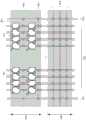
图5A示出了根据本公开的方面的显示面板110的第一光学区域OA1和普通区域NA中的每一者中的信号线的示例设置,并且图5B示出了根据本公开的方面的显示面板110的第二光学区域OA2和普通区域NA中的每一者中的信号线的示例设置。5A shows an example arrangement of signal lines in each of the first optical area OA1 and the normal area NA of the
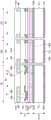
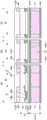
图5A和图5B中所示的第一水平显示区域HA1是显示面板110的第一水平显示区域HA1的部分。图5A和图5B中所示的第二水平显示区域HA2是显示面板110的第二水平显示区域HA2的部分。The first horizontal display area HA1 shown in FIGS. 5A and 5B is a portion of the first horizontal display area HA1 of the
图5A中所示的第一光学区域OA1为显示面板110的第一光学区域OA1的一部分,并且图5B中所示的第二光学区域OA2为显示面板110的第二光学区域OA2的一部分。The first optical area OA1 shown in FIG. 5A is a part of the first optical area OA1 of the
参考图5A和图5B,第一水平显示区域HA1可以包括普通区域NA的一部分、第一光学区域OA1和第二光学区域OA2。第二水平显示区域HA2可以包括普通区域NA的另一部分。Referring to FIGS. 5A and 5B , the first horizontal display area HA1 may include a portion of the normal area NA, the first optical area OA1 , and the second optical area OA2 . The second horizontal display area HA2 may include another part of the normal area NA.
各种类型的水平线(HL1和HL2)和各种类型的垂直线(VLn、VL1和VL2)可以被设置在显示面板110中。Various types of horizontal lines ( HL1 and HL2 ) and various types of vertical lines ( VLn, VL1 and VL2 ) may be provided in the
在一些实施方式中,术语“水平”和术语“垂直”用于指代与显示面板相交的两个方向;然而,应注意,水平方向和垂直方向可取决于观看方向而改变。水平方向可以指例如一条选通线GL延伸的方向,并且垂直方向可以指例如一条数据线DL延伸的方向。因此,术语“水平”和“垂直”用于表示两个方向。In some embodiments, the terms "horizontal" and the term "vertical" are used to refer to two directions that intersect the display panel; however, it should be noted that the horizontal and vertical directions may vary depending on the viewing direction. The horizontal direction may refer to, for example, the direction in which one gate line GL extends, and the vertical direction may refer to, for example, the direction in which one data line DL extends. Accordingly, the terms "horizontal" and "vertical" are used to denote both directions.
参考图5A和图5B,设置在显示面板110中的水平线可以包括设置在第一水平显示区域HA1中的第一水平线HL1和设置在第二水平显示区域HA2上的第二水平线HL2。Referring to FIGS. 5A and 5B , the horizontal lines disposed in the
设置在显示面板110中的水平线可以为选通线GL。也就是说,第一水平线HL1和第二水平线HL2可以是选通线GL。根据一个或更多个像素SP的结构,选通线GL可以包括各种类型的选通线。Horizontal lines disposed in the
参考图5A和图5B,设置在显示面板110中的垂直线可以包括仅设置在普通区域NA中的垂直线VLn、延伸穿过第一光学区域OA1和普通区域NA两者的第一垂直线VL1、以及延伸穿过第二光学区域OA2和普通区域NA两者的第二垂直线VL2。Referring to FIGS. 5A and 5B , vertical lines disposed in the
设置在显示面板110中的垂直线可以包括数据线DL、驱动电压线DVL等,并且还可以包括参考电压线、初始化电压线等。也就是说,普通垂直线VLn、第一垂直线VL1和第二垂直线VL2可以包括数据线DL、驱动电压线DVL等,并且还包括参考电压线、初始化电压线等。The vertical lines provided in the
在一些实施方式中,应注意,第二水平线HL2中的术语“水平”可意指仅显示面板的从左侧到右侧(或从右侧到左侧)承载信号,并且可能不意味着第二水平线HL2仅在直接水平方向上沿直线延伸。例如,在图5A和图5B中,虽然第二水平线HL2以直线示出,但是第二水平线HL2中的一条或更多条可以包括与图5A和图5B中示出的构造不同的一个或更多个弯曲或折叠部分。同样地,第一水平线HL1中的一条或更多条还可以包括一个或更多个弯曲或折叠部分。In some embodiments, it should be noted that the term "horizontal" in the second horizontal line HL2 may mean that only the display panel carries signals from left to right (or from right to left), and may not mean that the second The second horizontal line HL2 extends in a straight line only in the direct horizontal direction. For example, in FIGS. 5A and 5B , although the second horizontal lines HL2 are shown as straight lines, one or more of the second horizontal lines HL2 may include one or more different configurations from those shown in FIGS. 5A and 5B . Multiple curved or folded sections. Likewise, one or more of the first horizontal lines HL1 may also include one or more bent or folded portions.
在一些实施方式中,应注意,在典型垂直线VLn中的术语“垂直”可仅意味着显示面板的从上部到下部(或从下部到上部)承载信号,并且可以不表示典型垂直线VLn仅在直接垂直方向上沿直线延伸。例如,在图5A和图5B中,虽然以直线示出了典型的垂直线VLn,但是典型垂直线VLn中的一条或更多条可以包括与图5A和图5B中示出的构造不同的一个或更多个弯曲或折叠部分。同样地,第一垂直线VL1的一条或更多条和第二垂直线VL2中的一条或更多条还可以包括一个或更多个弯曲或折叠部分。In some embodiments, it should be noted that the term "vertical" in the typical vertical line VLn may only mean that the display panel carries signals from the upper part to the lower part (or from the lower part to the upper part), and may not mean that the typical vertical line VLn only Extends in a straight line in the immediate vertical direction. For example, in FIGS. 5A and 5B , although the typical vertical lines VLn are shown as straight lines, one or more of the typical vertical lines VLn may include a configuration different from that shown in FIGS. 5A and 5B . or more bent or folded sections. Likewise, one or more of the first vertical lines VL1 and one or more of the second vertical lines VL2 may further include one or more bent or folded portions.
参考图5A,包括在第一水平显示区域HA1中的第一光学区域OA1可以包括如图4所示的发光区域EA和第一透射区域TA1。在第一光学区域OA1中,第一透射区域TA1的相应外部区域可以包括在发光区域EA中。Referring to FIG. 5A , the first optical area OA1 included in the first horizontal display area HA1 may include the light emitting area EA and the first transmissive area TA1 as shown in FIG. 4 . In the first optical area OA1, a corresponding outer area of the first transmissive area TA1 may be included in the light emitting area EA.
参考图5A,为了提高第一光学区域OA1的透射率,第一水平线HL1可以延伸穿过第一光学区域OA1,同时避开第一光学区域OA1中的第一透射区域TA1。Referring to FIG. 5A , in order to improve the transmittance of the first optical area OA1 , the first horizontal line HL1 may extend through the first optical area OA1 while avoiding the first transmissive area TA1 in the first optical area OA1 .
因此,延伸穿过第一光学区域OA1的第一水平线HL1中的每一条可以包括围绕第一透射区域TA1中的一个或更多个的一个或更多个相应外边缘延伸的一个或更多个曲折或弯曲部分。Accordingly, each of the first horizontal lines HL1 extending through the first optical area OA1 may include one or more horizontal lines extending around one or more corresponding outer edges of one or more of the first transmissive areas TA1 . Twists or bends.
因此,设置在第一水平显示区域HA1中的第一水平线HL1和设置在第二水平显示区域HA2中的第二水平线HL2可以具有不同的形状或长度。例如,延伸穿过第一光学区域OA1的第一水平线HL1与未延伸穿过第一光学区域OA1的第二水平线HL2可以具有不同的形状或长度。Accordingly, the first horizontal line HL1 disposed in the first horizontal display area HA1 and the second horizontal line HL2 disposed in the second horizontal display area HA2 may have different shapes or lengths. For example, the first horizontal line HL1 extending through the first optical area OA1 and the second horizontal line HL2 not extending through the first optical area OA1 may have different shapes or lengths.
此外,为了改善第一光学区域OA1的透射率,第一垂直线VL1可以延伸穿过第一光学区域OA1,同时避开第一光学区域OA1中的第一透射区域TA1。In addition, in order to improve the transmittance of the first optical area OA1, the first vertical line VL1 may extend through the first optical area OA1 while avoiding the first transmissive area TA1 in the first optical area OA1.
因此,延伸穿过第一光学区域OA1的第一垂直线VL1中的每一者可以包括围绕第一透射区域TA1中的一个或更多个的一个或更多个相应外边缘延伸的一个或更多个弯折或弯曲部分。Accordingly, each of the first vertical lines VL1 extending through the first optical area OA1 may include one or more vertical lines extending around one or more respective outer edges of one or more of the first transmissive areas TA1 . Multiple bends or bends.
因此,延伸穿过第一光学区域OA1的第一垂直线VL1和设置在普通区域NA中而不延伸穿过第一光学区域OA1的普通垂直线VLn可以具有不同的形状或长度。Accordingly, the first vertical line VL1 extending through the first optical area OA1 and the normal vertical line VLn disposed in the normal area NA without extending through the first optical area OA1 may have different shapes or lengths.
参考图5A,包括在第一水平显示区域HA1中的第一光学区域OA1中的第一透射区域TA1可以沿对角线方向设置。Referring to FIG. 5A , the first transmissive area TA1 included in the first optical area OA1 in the first horizontal display area HA1 may be disposed in a diagonal direction.
参考图5A,在第一水平显示区域HA1中的第一光学区域OA1中,一个或更多个发光区域EA可以被设置在两个水平相邻的第一透射区域TA1之间。在第一水平显示区域HA1中的第一光学区域OA1中,一个或更多个发光区域EA可以沿上下方向(例如,两个垂直相邻的第一透射区域TA1)设置在彼此相邻的两个第一透射区域TA1之间。Referring to FIG. 5A , in the first optical area OA1 in the first horizontal display area HA1 , one or more light emitting areas EA may be disposed between two horizontally adjacent first transmissive areas TA1 . In the first optical area OA1 in the first horizontal display area HA1, one or more light emitting areas EA may be disposed on two sides adjacent to each other along the up-down direction (for example, two vertically adjacent first transmissive areas TA1). Between the first transmission areas TA1.
参考图5A,设置在第一水平显示区域HA1中的第一水平线HL1中的每一者(例如,延伸穿过第一光学区域OA1的第一水平线HL1中的每一者)可以包括围绕第一透射区域TA1中的一个或更多个的一个或更多个相应外边缘延伸的一个或更多个弯折或弯曲部分。Referring to FIG. 5A , each of the first horizontal lines HL1 disposed in the first horizontal display area HA1 (for example, each of the first horizontal lines HL1 extending through the first optical area OA1 ) may include One or more bends or bent portions of one or more respective outer edges of one or more of the transmissive areas TA1 extend.
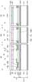
参考图5B,包括在第一水平显示区域HA1中的第二光学区域OA2可以包括发光区域EA和第二透射区域TA2。在第二光学区域OA2中,第二透射区域TA2的相应外部区域可以被包括在发光区域EA中。Referring to FIG. 5B , the second optical area OA2 included in the first horizontal display area HA1 may include a light emitting area EA and a second transmissive area TA2 . In the second optical area OA2, a corresponding outer area of the second transmissive area TA2 may be included in the light emitting area EA.
在一个实施方式中,第二光学区域OA2中的发光区域EA和第二透射区域TA2可以具有与图5A的第一光学区域OA1中的发光区域EA和第一透射区域TA1基本上相同的位置和设置。In one embodiment, the light emitting area EA and the second transmissive area TA2 in the second optical area OA2 may have substantially the same positions and positions as the light emitting area EA and the first transmissive area TA1 in the first optical area OA1 of FIG. 5A . set up.
在另一实施方式中,如图5B所示,第二光学区域OA2中的发光区域EA和第二透射区域TA2可以具有与图5A的第一光学区域OA1中的发光区域EA和第一透射区域TA1不同的位置和设置。In another embodiment, as shown in FIG. 5B , the light-emitting area EA and the second transmissive area TA2 in the second optical area OA2 may have the same shape as the light-emitting area EA and the first transmissive area in the first optical area OA1 in FIG. 5A . TA1 different locations and settings.
例如,参考图5B,第二光学区域OA2中的第二透射区域TA2可以沿水平方向(从左到右或者从右到左)设置。在该示例中,发光区域EA可以不沿左右方向(例如,水平方向)彼此相邻地设置在两个第二透射区域TA2之间。此外,第二光学区域OA2中的发光区域EA中的一个或更多个可以被设置在沿上下方向(例如,垂直方向)彼此相邻的第二透射区域TA2之间。例如,一个或更多个发光区域EA可以被设置在两行第二透射区域之间。For example, referring to FIG. 5B , the second transmissive area TA2 in the second optical area OA2 may be disposed in a horizontal direction (from left to right or from right to left). In this example, the light emitting area EA may not be disposed adjacent to each other in a left-right direction (eg, a horizontal direction) between two second transmissive areas TA2 . In addition, one or more of the light emitting areas EA in the second optical area OA2 may be disposed between the second transmissive areas TA2 adjacent to each other in an up-down direction (eg, a vertical direction). For example, one or more light emitting areas EA may be disposed between two rows of second transmissive areas.
当在第一水平显示区域HA1中,第一水平线HL1延伸穿过第二光学区域OA2和与第二光学区域OA2相邻的普通区域NA时,在一个实施方式中,第一水平线HL1可以具有与图5A的第一水平线HL1基本上相同的设置。When in the first horizontal display area HA1, the first horizontal line HL1 extends through the second optical area OA2 and the normal area NA adjacent to the second optical area OA2, in one embodiment, the first horizontal line HL1 may have the same The first horizontal line HL1 of FIG. 5A is basically the same arrangement.
在另一实施方式中,如图5B中所示,当在第一水平显示区域HA1中,延伸穿过第二光学区域OA2和与第二光学区域OA2相邻的普通区域NA时,第一水平线HL1可以具有与图5A的第一水平线HL1不同的设置。In another embodiment, as shown in FIG. 5B , when extending through the second optical area OA2 and the normal area NA adjacent to the second optical area OA2 in the first horizontal display area HA1 , the first horizontal line HL1 may have a different setting from the first horizontal line HL1 of FIG. 5A .
这是因为图5B的第二光学区域OA2中的发光区域EA和第二透射区域TA2具有与图5A的第一光学区域OA1中的发光区域EA和第一透射区域TA1不同的位置和设置。This is because the light emitting area EA and the second transmissive area TA2 in the second optical area OA2 of FIG. 5B have different positions and arrangements from the light emitting area EA and the first transmissive area TA1 in the first optical area OA1 of FIG. 5A .
参考图5B,当在第一水平显示区域HA1中,第一水平线HL1延伸穿过第二光学区域OA2和与第二光学区域OA2相邻的普通区域NA时,第一水平线HL1可以以直线在垂直相邻的第二透射区域TA2之间延伸而不具有弯折或弯曲部分。Referring to FIG. 5B, when in the first horizontal display area HA1, the first horizontal line HL1 extends through the second optical area OA2 and the normal area NA adjacent to the second optical area OA2, the first horizontal line HL1 may be vertically aligned in a straight line. Adjacent second transmissive areas TA2 extend between each other without a bent or curved portion.
例如,一条第一水平线HL1可以在第一光学区域OA1中具有一个或更多个弯折或弯曲部分,但是在第二光学区域OA2中可以不具有弯折或弯曲部分。For example, a first horizontal line HL1 may have one or more bends or curved portions in the first optical area OA1, but may have no bends or curved portions in the second optical area OA2.
为了改善第二光学区域OA2的透射率,第二垂直线VL2可以延伸穿过第二光学区域OA2,同时避开第二光学区域OA2中的第二透射区域TA2。In order to improve the transmittance of the second optical area OA2, the second vertical line VL2 may extend through the second optical area OA2 while avoiding the second transmissive area TA2 in the second optical area OA2.
因此,延伸穿过第二光学区域OA2的第二垂直线VL2中的每一者可以包括围绕第二透射区域TA2中的一个或更多个的一个或更多个相应外边缘延伸的一个或更多个弯折或弯曲部分。Accordingly, each of the second vertical lines VL2 extending through the second optical area OA2 may include one or more vertical lines extending around one or more respective outer edges of one or more of the second transmissive areas TA2. Multiple bends or bends.
因此,延伸穿过第二光学区域OA2的第二垂直线VL2与设置在普通区域NA中而不穿过第二光学区域OA2的普通垂直线VLn可以具有不同的形状或长度。Accordingly, the second vertical line VL2 extending through the second optical area OA2 may have a different shape or length from the normal vertical line VLn disposed in the normal area NA without passing through the second optical area OA2.
如图5A所示,延伸穿过第一光学区域OA1的第一水平线HL1中的每一者或一个或更多个可以具有围绕第一透射区域TA1中的一个或更多个的一个或更多个相应外边缘延伸的一个或更多个弯折或弯曲部分。As shown in FIG. 5A , each or one or more of the first horizontal lines HL1 extending through the first optical area OA1 may have one or more One or more bends or bends extending from a corresponding outer edge.
因此,延伸穿过第一光学区域OA1和第二光学区域OA2的第一水平线HL1的长度可以稍长于仅设置在普通区域NA中而不穿过第一光学区域OA1和第二光学区域OA2的第二水平线HL2的长度。Therefore, the length of the first horizontal line HL1 extending through the first optical area OA1 and the second optical area OA2 may be slightly longer than that of the first horizontal line HL1 provided only in the normal area NA without passing through the first optical area OA1 and the second optical area OA2. The length of the second horizontal line HL2.
因此,延伸穿过第一光学区域OA1和第二光学区域OA2的第一水平线HL1的电阻(被称为第一电阻)可以略大于仅设置在普通区域NA中而不穿过第一光学区域OA1和第二光学区域OA2的第二水平线HL2的电阻(其被称为第二电阻)。Therefore, the resistance (referred to as the first resistance) of the first horizontal line HL1 extending through the first optical area OA1 and the second optical area OA2 may be slightly larger than that provided only in the normal area NA without passing through the first optical area OA1. and the resistance of the second horizontal line HL2 of the second optical area OA2 (which is referred to as the second resistance).
参考图5A和图5B,根据示例光透射结构,至少部分地与第一光学电子装置11交叠的第一光学区域OA1包括第一透射区域TA1,并且与第二光学电子装置12至少部分地交叠的第二光学区域OA2包括第二透射区域TA2。因此,第一光学区域OA1和第二光学区域OA2中的每一者中每单位面积的像素数量可以小于普通区域NA的像素数量。Referring to FIG. 5A and FIG. 5B, according to an example light transmission structure, the first optical area OA1 at least partially overlapping the first optical
因此,连接到延伸穿过第一光学区域OA1和第二光学区域OA2的第一水平线HL1中的每一者或一条或更多条的像素的数量可以不同于连接到仅设置在普通区域NA中而不延伸穿过第一光学区域OA1和第二光学区域OA2的第二水平线HL2中的每一者或一条或更多条的像素的数量。Therefore, the number of pixels connected to each of or one or more of the first horizontal lines HL1 extending through the first optical area OA1 and the second optical area OA2 may be different from that connected to the pixels provided only in the normal area NA. The number of pixels that do not extend through each or one or more of the second horizontal lines HL2 of the first optical area OA1 and the second optical area OA2 .
连接到延伸穿过第一光学区域OA1和第二光学区域OA2的第一水平线HL1中的每一者或一条或更多条的像素的数量(其被称作第一数量)可以小于连接到仅设置在普通区域NA中而不延伸穿过第一光学区域OA1和第二光学区域OA2的第二水平线HL2中的每一者或一条或更多条的像素的数量(其被称作第二数量)。The number of pixels connected to each or one or more of the first horizontal lines HL1 extending through the first optical area OA1 and the second optical area OA2 (which is referred to as a first number) may be smaller than those connected to only The number of pixels disposed in the normal area NA without extending through each or one or more of the second horizontal lines HL2 of the first optical area OA1 and the second optical area OA2 (which is referred to as a second number ).
第一数量与第二数量之间的差可以根据第一光学区域OA1与第二光学区域OA2中的每一者的分辨率与普通区域NA的分辨率之间的差而变化。例如,当第一光学区域OA1与第二光学区域OA2中的每一者的分辨率与普通区域NA的分辨率之间的差增大时,第一数量与第二数量之间的差可以增大。The difference between the first number and the second number may vary according to the difference between the resolution of each of the first and second optical areas OA1 and OA2 and the resolution of the normal area NA. For example, when the difference between the resolution of each of the first optical area OA1 and the second optical area OA2 and the resolution of the normal area NA increases, the difference between the first amount and the second amount may increase. big.
如上所述,由于连接到延伸穿过第一光学区域OA1和第二光学区域OA2的第一水平线HL1中的每一者或一条或更多条的像素的数量(第一数量)小于连接到仅设置在普通区域NA中而不延伸穿过第一光学区域OA1和第二光学区域OA2的第二水平线HL2中的每一者或一条或更多条的像素的数量(第二数量),所以第一水平线HL1与邻近第一水平线HL1的一个或更多个其他电极或线交叠的区域可以小于第二水平线HL2与邻近第二水平线HL2的一个或更多个其他电极或线交叠的区域。As described above, since the number of pixels (first number) connected to each or one or more of the first horizontal lines HL1 extending through the first optical area OA1 and the second optical area OA2 is smaller than that connected to only The number of pixels (second number) provided in the normal area NA without extending through each of the second horizontal lines HL2 of the first optical area OA1 and the second optical area OA2 or one or more (second number) An area where a horizontal line HL1 overlaps with one or more other electrodes or lines adjacent to the first horizontal line HL1 may be smaller than an area where a second horizontal line HL2 overlaps with one or more other electrodes or lines adjacent to the second horizontal line HL2.
因此,形成在第一水平线HL1与邻近于第一水平线HL1的一个或更多个其他电极或线之间的寄生电容(其被称作第一电容)可以远小于形成在第二水平线HL2与邻近于第二水平线HL2的一个或更多个其他电极或线之间的寄生电容(其被称作第二电容)。Therefore, the parasitic capacitance (which is referred to as a first capacitance) formed between the first horizontal line HL1 and one or more other electrodes or lines adjacent to the first horizontal line HL1 can be much smaller than that formed between the second horizontal line HL2 and the adjacent electrodes or lines. A parasitic capacitance (which is referred to as a second capacitance) between one or more other electrodes or lines of the second horizontal line HL2.
考虑到第一电阻与第二电阻之间的大小关系(第一电阻≥第二电阻)以及第一电容与第二电容之间的大小关系(第一电容<<第二电容),延伸穿过第一光学区域OA1和第二光学区域OA2的第一水平线HL1的电阻电容(RC)值(其被称作第一RC值)可以远小于仅设置在普通区域NA中而不延伸穿过第一光学区域OA1和第二光学区域OA2的第二水平线HL2的RC值(其被称作第二RC值)。因此,在该示例中,第一RC值远小于第二RC值(即,第一RC值<<第二RC值)。Considering the size relationship between the first resistance and the second resistance (first resistance ≥ second resistance) and the size relationship between the first capacitance and the second capacitance (first capacitance << second capacitance), extending through The resistance-capacitance (RC) value of the first horizontal line HL1 of the first optical area OA1 and the second optical area OA2 (which is referred to as a first RC value) may be much smaller than that which is only provided in the normal area NA without extending through the first horizontal line HL1. The RC value of the optical area OA1 and the second horizontal line HL2 of the second optical area OA2 (which is referred to as a second RC value). Thus, in this example, the first RC value is much smaller than the second RC value (ie, first RC value<<second RC value).
由于第一水平线HL1的第一RC值与第二水平线HL2的第二RC值之间的这种差(其被称为RC负载差),通过第一水平线HL1的信号传输特性可以与通过第二水平线HL2的信号传输特性不同。Due to this difference between the first RC value of the first horizontal line HL1 and the second RC value of the second horizontal line HL2 (which is referred to as RC load difference), the signal transmission characteristic through the first horizontal line HL1 can be compared with that through the second RC value. The signal transmission characteristics of the horizontal line HL2 are different.
图6和图7是根据本公开的方面的包括在显示面板110的显示区域DA中的第一光学区域(例如,上述附图中的第一光学区域OA1)、第二光学区域(例如,上述附图中的第二光学区域OA2)和普通区域(例如,上述附图中的普通区域NA)中的每一者的示例性横截面图。6 and 7 are diagrams showing the first optical area (for example, the first optical area OA1 in the above-mentioned figures), the second optical area (for example, the above-mentioned Exemplary cross-sectional views of each of the second optical area (OA2) in the drawings and a normal area (eg, the normal area NA in the above-mentioned figures).
图6示出了在触摸传感器以触摸面板的形式存在于显示面板110外部的示例中的显示面板(例如,上述附图中的显示面板110)。图7示出了在触摸传感器TS存在于显示面板110内部的示例中的显示面板(例如,上述附图中的显示面板110)。FIG. 6 illustrates a display panel (for example, the
图6和图7中的每一者示出了包括在显示区域DA中的普通区域NA、第一光学区域OA1和第二光学区域OA2的示例横截面图。Each of FIGS. 6 and 7 shows an example cross-sectional view of the normal area NA, the first optical area OA1 , and the second optical area OA2 included in the display area DA.
首先,将参考图6和图7描述普通区域NA的堆叠结构。第一光学区域OA1和第二光学区域OA2的相应发光区域EA可以具有与普通区域NA的发光区域EA相同的堆叠结构。First, the stack structure of the normal area NA will be described with reference to FIGS. 6 and 7 . The corresponding light emitting areas EA of the first and second optical areas OA1 and OA2 may have the same stack structure as that of the light emitting areas EA of the normal area NA.
参考图6和图7,基板SUB可以包括第一基板SUB1、层间绝缘层IPD和第二基板SUB2。层间绝缘层IPD可以插入在第一基板SUB1与第二基板SUB2之间。由于基板SUB包括第一基板SUB1、层间绝缘层IPD和第二基板SUB2,因此基板SUB可以防止或减少水分的渗透。第一基板SUB1和第二基板SUB2可以是例如聚酰亚胺(PI)基板。第一基板SUB1可以被称为主PI基板,并且第二基板SUB2可以被称为副PI基板。Referring to FIGS. 6 and 7 , the substrate SUB may include a first substrate SUB1, an insulating interlayer IPD, and a second substrate SUB2. An insulating interlayer IPD may be interposed between the first substrate SUB1 and the second substrate SUB2. Since the substrate SUB includes the first substrate SUB1, the interlayer insulating layer IPD, and the second substrate SUB2, the substrate SUB can prevent or reduce moisture penetration. The first substrate SUB1 and the second substrate SUB2 may be, for example, polyimide (PI) substrates. The first substrate SUB1 may be called a main PI substrate, and the second substrate SUB2 may be called a sub PI substrate.
参考图6和图7,用于设置诸如驱动晶体管DRT等的一个或更多个晶体管的各种类型的图案ACT、SD1、GATE、各种类型的绝缘层MBUF、ABUF1、ABUF2、GI、ILD1、ILD2、PAS0和各种类型的金属图案TM、GM、ML1、ML2可以被设置在基板SUB上或上方。Referring to FIGS. 6 and 7, various types of patterns ACT, SD1, GATE, various types of insulating layers MBUF, ABUF1, ABUF2, GI, ILD1, ILD2, PAS0 and various types of metal patterns TM, GM, ML1, ML2 may be disposed on or over the substrate SUB.
参考图6和图7,多缓冲层MBUF可以被设置在第二基板SUB2上,并且第一有源缓冲层ABUF1可以被设置在多缓冲层MBUF上。Referring to FIGS. 6 and 7 , the multi-buffer layer MBUF may be disposed on the second substrate SUB2, and the first active buffer layer ABUF1 may be disposed on the multi-buffer layer MBUF.
第一金属层ML1和第二金属层ML2可以被设置在第一有源缓冲层ABUF1上。例如,第一金属层ML1和第二金属层ML2可以是用于屏蔽光的光屏蔽层LS。The first metal layer ML1 and the second metal layer ML2 may be disposed on the first active buffer layer ABUF1. For example, the first metal layer ML1 and the second metal layer ML2 may be a light shielding layer LS for shielding light.
第二有源缓冲层ABUF2可以被设置在第一金属层ML1和第二金属层ML2上。驱动晶体管DRT的有源层ACT可以被设置在第二有源缓冲层ABUF2上。The second active buffer layer ABUF2 may be disposed on the first and second metal layers ML1 and ML2. The active layer ACT of the driving transistor DRT may be disposed on the second active buffer layer ABUF2.
栅极绝缘层GI可以被设置为覆盖有源层ACT。A gate insulating layer GI may be disposed to cover the active layer ACT.
驱动晶体管DRT的栅极GATE可以被设置在栅极绝缘层GI上。此外,栅极材料层GM可以连同驱动晶体管DRT的栅极GATE一起在与设置驱动晶体管DRT的位置不同的位置处设置在栅极绝缘层GI上。The gate GATE of the driving transistor DRT may be disposed on the gate insulating layer GI. In addition, the gate material layer GM may be disposed on the gate insulating layer GI at a position different from the position where the driving transistor DRT is disposed together with the gate GATE of the driving transistor DRT.
第一层间绝缘层ILD1可以被设置为覆盖栅极GATE和栅极材料层GM。金属图案TM可以被设置在第一层间绝缘层ILD1上。金属图案TM可以位于与形成驱动晶体管DRT的位置不同的位置处。第二层间绝缘层ILD2可以被设置为覆盖第一层间绝缘层ILD1上的金属图案TM。The first interlayer insulating layer ILD1 may be disposed to cover the gate GATE and the gate material layer GM. A metal pattern TM may be disposed on the first insulating interlayer layer ILD1. The metal pattern TM may be located at a location different from that where the driving transistor DRT is formed. The second insulating interlayer ILD2 may be disposed to cover the metal pattern TM on the first insulating interlayer ILD1.
两个第一源极-漏极电极图案SD1可以被设置在第二层间绝缘层ILD2上。两个第一源极-漏极电极图案SD1中的一个可以是驱动晶体管DRT的源极节点,而另一个可以是驱动晶体管DRT的漏极节点。Two first source-drain electrode patterns SD1 may be disposed on the second insulating interlayer layer ILD2. One of the two first source-drain electrode patterns SD1 may be a source node of the driving transistor DRT, and the other may be a drain node of the driving transistor DRT.
两个第一源极-漏极电极图案SD1可以通过形成在第二层间绝缘层ILD2、第一层间绝缘层ILD1和栅极绝缘层GI中的接触孔分别电连接到有源层ACT的第一侧部和第二侧部。The two first source-drain electrode patterns SD1 may be electrically connected to the active layer ACT through contact holes formed in the second interlayer insulating layer ILD2, the first interlayer insulating layer ILD1, and the gate insulating layer GI, respectively. a first side and a second side.
有源层ACT的与栅极GATE交叠的部分可以用作沟道区域。两个第一源极-漏极电极图案SD1中的一个可以连接到有源层ACT的沟道区域的第一侧部,并且两个第一源极-漏极电极图案SD1中的另一个可以连接到有源层ACT的沟道区域的第二侧部。A portion of the active layer ACT overlapping the gate GATE may serve as a channel region. One of the two first source-drain electrode patterns SD1 may be connected to a first side of the channel region of the active layer ACT, and the other of the two first source-drain electrode patterns SD1 may connected to the second side of the channel region of the active layer ACT.
钝化层PAS0可以被设置为覆盖两个第一源极-漏极电极图案SD1。平坦化层PLN可以被设置在钝化层PAS0上。平坦化层PLN可以包括第一平坦化层PLN1和第二平坦化层PLN2。A passivation layer PAS0 may be disposed to cover the two first source-drain electrode patterns SD1. A planarization layer PLN may be disposed on the passivation layer PAS0. The planarization layer PLN may include a first planarization layer PLN1 and a second planarization layer PLN2.
第一平坦化层PLN1可以被设置在钝化层PAS0上。The first planarization layer PLN1 may be disposed on the passivation layer PAS0.
第二源极-漏极电极图案SD2可以被设置在第一平坦化层PLN1上。第二源极-漏极电极图案SD2可以通过形成在第一平坦化层PLN1中的接触孔连接到两个第一源极-漏极电极图案SD1中的一个(对应于图3的像素SP中的驱动晶体管DRT的第二节点N2)。The second source-drain electrode pattern SD2 may be disposed on the first planarization layer PLN1. The second source-drain electrode pattern SD2 may be connected to one of the two first source-drain electrode patterns SD1 through a contact hole formed in the first planarization layer PLN1 (corresponding to the one in the pixel SP of FIG. 3 ). The second node N2 of the driving transistor DRT).
第二平坦化层PLN2可以被设置为覆盖第二源极-漏极电极图案SD2。发光元件ED可以被设置在第二平坦化层PLN2上。The second planarization layer PLN2 may be disposed to cover the second source-drain electrode pattern SD2. The light emitting element ED may be disposed on the second planarization layer PLN2.
根据发光元件ED的示例堆叠结构,阳极AE可以被设置在第二平坦化层PLN2上。阳极AE可以通过形成在第二平坦化层PLN2中的接触孔与第二源极-漏极电极图案SD2电连接。According to an example stack structure of the light emitting element ED, the anode AE may be disposed on the second planarization layer PLN2. The anode AE may be electrically connected to the second source-drain electrode pattern SD2 through a contact hole formed in the second planarization layer PLN2.
堤部BANK可以被设置为覆盖阳极AE的一部分。可以打开与像素SP的发光区域EA相对应的堤部BANK的一部分。The bank BANK may be provided to cover a part of the anode AE. A portion of the bank BANK corresponding to the light emitting area EA of the pixel SP may be turned on.
阳极AE的一部分可以通过堤部BANK的开口(开口部分)暴露。发光层EL可以被设置在堤部BANK的侧表面上和堤部BANK的开口(打开部分)中。发光层EL的全部或至少一部分可以位于相邻堤部之间。A part of the anode AE may be exposed through the opening (opening portion) of the bank BANK. The light emitting layer EL may be provided on the side surface of the bank BANK and in the opening (open portion) of the bank BANK. All or at least a part of the light emitting layer EL may be located between adjacent banks.
在堤部BANK的开口中,发光层EL可以接触阳极AE。阴极CE可以被设置在发光层EL上。In the opening of the bank BANK, the light emitting layer EL may contact the anode AE. The cathode CE may be disposed on the light emitting layer EL.
发光元件ED可通过包括如上所述的阳极AE、发光层EL和阴极CE来形成。发光层EL可以包括有机材料层。The light emitting element ED can be formed by including the anode AE, the light emitting layer EL, and the cathode CE as described above. The light emitting layer EL may include an organic material layer.
封装层ENCAP可以被设置在发光元件ED的堆叠上。An encapsulation layer ENCAP may be arranged on the stack of light emitting elements ED.
例如,如图6和图7所示,封装层ENCAP可以具有单层结构或多层结构,封装层ENCAP可以包括第一封装层PAS1、第二封装层PCL和第三封装层PAS2。For example, as shown in FIGS. 6 and 7 , the encapsulation layer ENCAP may have a single-layer structure or a multi-layer structure, and the encapsulation layer ENCAP may include a first encapsulation layer PAS1 , a second encapsulation layer PCL and a third encapsulation layer PAS2 .
第一封装层PAS1和第三封装层PAS2可以是例如无机材料层,而第二封装层PCL可以是例如有机材料层。在第一封装层PAS1、第二封装层PCL和第三封装层PAS2中,第二封装层PCL可以为最厚的并用作平坦化层。The first encapsulation layer PAS1 and the third encapsulation layer PAS2 may be, for example, inorganic material layers, while the second encapsulation layer PCL may be, for example, an organic material layer. Among the first encapsulation layer PAS1 , the second encapsulation layer PCL, and the third encapsulation layer PAS2 , the second encapsulation layer PCL may be the thickest and serve as a planarization layer.
第一封装层PAS1可以被设置在阴极CE上,并且可以被设置为最接近发光元件ED。第一封装层PAS1可以包括能够使用低温沉积来沉积的无机绝缘材料。例如,第一封装层PAS1可以包括但不限于硅氮化物(SiNx)、硅氧化物(SiOx)、氮氧化硅(SiON)、氧化铝(Al2O3)等。由于第一封装层PAS1可以在低温气氛中沉积,所以在沉积工艺期间,第一封装层PAS1可以防止包括有机材料的发光层EL受到高温气氛的损坏。The first encapsulation layer PAS1 may be disposed on the cathode CE, and may be disposed closest to the light emitting element ED. The first encapsulation layer PAS1 may include an inorganic insulating material capable of being deposited using low temperature deposition. For example, the first encapsulation layer PAS1 may include, but not limited to, silicon nitride (SiNx), silicon oxide (SiOx), silicon oxynitride (SiON), aluminum oxide (Al2 O3 ), and the like. Since the first encapsulation layer PAS1 may be deposited in a low temperature atmosphere, the first encapsulation layer PAS1 may prevent the light emitting layer EL including an organic material from being damaged by a high temperature atmosphere during the deposition process.
第二封装层PCL可以具有比第一封装层PAS1更小的面积或尺寸。例如,第二封装层PCL可以被设置为暴露第一封装层PAS1的两端或边缘。第二封装层PCL可以充当用于在显示装置100弯折或弯曲时减轻对应层之间的应力的缓冲并且还用于增强平坦化性能。例如,第二封装层PCL可以包括有机绝缘材料,诸如,丙烯酸树脂、环氧树脂、聚酰亚胺、聚乙烯、碳氧化硅(SiOC)等。第二封装层PCL可以例如使用喷墨技术来设置。The second encapsulation layer PCL may have a smaller area or size than the first encapsulation layer PAS1. For example, the second encapsulation layer PCL may be configured to expose both ends or edges of the first encapsulation layer PAS1. The second encapsulation layer PCL may serve as a buffer for alleviating stress between corresponding layers when the
第三封装层PAS2可以被设置在基板SUB上方,第二封装层PCL被设置在基板SUB上方,使得第三封装层PAS2覆盖第二封装层PCL和第一封装层PAS1的相应顶面和侧面。第三封装层PAS2可以最小化或防止外部水分或氧气渗透到第一封装层PAS1和第二封装层PCL中。例如,第三封装层PAS2可以包括无机绝缘材料,诸如,硅氮化物(SiNx)、硅氧化物(SiOx)、氮氧化硅(SiON)、氧化铝(Al2O3)等。The third encapsulation layer PAS2 may be disposed over the substrate SUB, and the second encapsulation layer PCL is disposed over the substrate SUB such that the third encapsulation layer PAS2 covers respective top and side surfaces of the second encapsulation layer PCL and the first encapsulation layer PAS1 . The third encapsulation layer PAS2 may minimize or prevent external moisture or oxygen from penetrating into the first encapsulation layer PAS1 and the second encapsulation layer PCL. For example, the third encapsulation layer PAS2 may include an inorganic insulating material such as silicon nitride (SiNx), silicon oxide (SiOx), silicon oxynitride (SiON), aluminum oxide (Al2 O3 ), and the like.
参考图7,在触摸传感器TS被嵌入到显示面板110中的示例中,包括触摸传感器TS的触摸传感器层TSL可以被设置在封装层ENCAP上。下面将详细描述触摸传感器层的结构。Referring to FIG. 7 , in an example where the touch sensor TS is embedded in the
触摸缓冲层T-BUF可以被设置在封装层ENCAP上。触摸传感器TS可以被设置在触摸缓冲层T-BUF上。The touch buffer layer T-BUF may be disposed on the encapsulation layer ENCAP. The touch sensor TS may be disposed on the touch buffer layer T-BUF.
触摸传感器TS可以包括位于不同层中的触摸传感器金属TSM和至少一个桥接金属BRG。The touch sensor TS may include a touch sensor metal TSM and at least one bridge metal BRG in different layers.
触摸层间绝缘层T-ILD可以被设置在触摸传感器金属TSM与桥接金属BRG之间。The touch interlayer insulating layer T-ILD may be disposed between the touch sensor metal TSM and the bridge metal BRG.
例如,触摸传感器金属TSM可以包括彼此相邻设置的第一触摸传感器金属TSM、第二触摸传感器金属TSM和第三触摸传感器金属TSM。在第三触摸传感器金属TSM被设置在第一触摸传感器金属TSM与第二触摸传感器金属TSM之间并且第一触摸传感器金属TSM和第二触摸传感器金属TSM需要彼此电连接的实施方式中,第一触摸传感器金属TSM和第二触摸传感器金属TSM可以通过位于不同层中的桥接金属BRG彼此电连接。桥接金属BRG可以通过触摸层间绝缘层T-ILD与第三触摸传感器金属TSM电绝缘。For example, the touch sensor metal TSM may include a first touch sensor metal TSM, a second touch sensor metal TSM, and a third touch sensor metal TSM disposed adjacent to each other. In an embodiment where the third touch sensor metal TSM is disposed between the first touch sensor metal TSM and the second touch sensor metal TSM and the first touch sensor metal TSM and the second touch sensor metal TSM need to be electrically connected to each other, the first The touch sensor metal TSM and the second touch sensor metal TSM may be electrically connected to each other through the bridge metal BRG located in different layers. The bridging metal BRG may be electrically insulated from the third touch sensor metal TSM by the touch interlayer insulating layer T-ILD.
当触摸传感器TS被设置在显示面板110上时,可能产生或引入在对应工艺中使用的化学溶液(例如,显影剂或蚀刻剂)或来自外部的水分。在一些实施方式中,通过将触摸传感器TS设置在触摸缓冲层T-BUF上,可以防止化学溶液或水分在触摸传感器TS的制造过程期间渗透到包括有机材料的发光层EL中。因此,触摸缓冲层T-BUF可以防止损坏容易受到化学溶液或水分的影响的发光层EL。When the touch sensor TS is disposed on the
为了防止对包括易受高温影响的有机材料的发光层EL的损坏,触摸缓冲层T-BUF可以在小于或等于预定温度(例如,100度(℃))的低温下形成,并且使用具有1至3的低介电常数的有机绝缘材料形成。例如,触摸缓冲层T-BUF可以包括丙烯酸基、环氧基或硅氧烷基材料。随着显示装置100被弯曲,封装层ENCAP可能被损坏,并且位于触摸缓冲层T-BUF上的触摸传感器金属可能破裂或断裂。即使当显示装置100被弯曲时,具有作为有机绝缘材料的平坦化性能的触摸缓冲层T-BUF可以防止封装层ENCAP的损坏和/或包括在触摸传感器TS中的金属(TSM、BRG)的破裂或断裂。In order to prevent damage to the light emitting layer EL including an organic material susceptible to high temperature, the touch buffer layer T-BUF may be formed at a low temperature less than or equal to a predetermined temperature (for example, 100 degrees (°C)), and use a 3 low dielectric constant organic insulating material. For example, the touch buffer layer T-BUF may include acrylic-based, epoxy-based or silicone-based materials. As the
可以设置保护层PAC以覆盖触摸传感器TS。保护层PAC可以是例如有机绝缘层。A protective layer PAC may be provided to cover the touch sensor TS. The protective layer PAC may be, for example, an organic insulating layer.
接下来,将参考图6和图7描述第一光学区域OA1的堆叠结构。Next, the stack structure of the first optical area OA1 will be described with reference to FIGS. 6 and 7 .
参考图6和图7,第一光学区域OA1的发光区域EA可以具有与在普通区域NA中的堆叠结构相同的堆叠结构。因此,在以下讨论中,将在下面详细描述第一光学区域OA1的第一透射区域TA1的堆叠结构,而不重复地描述第一光学区域OA1的发光区域EA。Referring to FIGS. 6 and 7 , the light emitting area EA of the first optical area OA1 may have the same stack structure as that in the normal area NA. Therefore, in the following discussion, the stacked structure of the first transmissive area TA1 of the first optical area OA1 will be described in detail below without repeatedly describing the light emitting area EA of the first optical area OA1.
在一些实施方式中,阴极CE可以被设置在包括在普通区域NA和第一光学区域OA1中的发光区域EA中,但是可以不被设置在第一光学区域OA1中的第一透射区域TA1中。例如,第一光学区域OA1的第一透射区域TA1可以对应于阴极CE的开口。In some embodiments, the cathode CE may be disposed in the light emitting area EA included in the normal area NA and the first optical area OA1, but may not be disposed in the first transmissive area TA1 in the first optical area OA1. For example, the first transmissive area TA1 of the first optical area OA1 may correspond to the opening of the cathode CE.
此外,在一些实施方式中,包括第一金属层ML1和第二金属层ML2中的至少一个的光屏蔽层LS可以被设置在包括在普通区域NA和第一光学区域OA1中的发光区域EA中,但是可以不被设置在第一光学区域OA1的第一透射区域TA1中。例如,第一光学区域OA1的第一透射区域TA1可以对应于光屏蔽层LS的开口。Also, in some embodiments, the light shielding layer LS including at least one of the first metal layer ML1 and the second metal layer ML2 may be disposed in the light emitting area EA included in the normal area NA and the first optical area OA1 , but may not be disposed in the first transmissive area TA1 of the first optical area OA1. For example, the first transmissive area TA1 of the first optical area OA1 may correspond to the opening of the light shielding layer LS.
基板SUB和设置在包括在普通区域NA和第一光学区域OA1中的发光区域EA中的各种类型的绝缘层(MBUF、ABUF1、ABUF2、GI、ILD1、ILD2、PAS0、PLN(PLN1、PLN2)、BANK、ENCAP(PAS1、PCL、PAS2)、T-BUF、T-ILD、PAC)可以同样地、基本上同样地或类似地设置在第一光学区域OA1中的第一透射区域TA1中。The substrate SUB and various types of insulating layers (MBUF, ABUF1, ABUF2, GI, ILD1, ILD2, PAS0, PLN (PLN1, PLN2) disposed in the light emitting area EA included in the normal area NA and the first optical area OA1 , BANK, ENCAP (PAS1, PCL, PAS2), T-BUF, T-ILD, PAC) may be identically, substantially identically, or similarly disposed in the first transmissive area TA1 in the first optical area OA1.
然而,在一些实施方式中,除了设置在包括在普通区域NA和第一光学区域OA1中的发光区域EA中的绝缘材料或层之外,具有电特性的一个或更多个材料层中的全部或一个或更多个(例如,一个或更多个金属材料层和/或一个或更多个半导体层)可以不被设置在第一光学区域OA1中的第一透射区域TA1中。However, in some embodiments, all of the one or more material layers having electrical properties except for the insulating material or layer disposed in the light emitting area EA included in the normal area NA and the first optical area OA1 Or one or more (eg, one or more metal material layers and/or one or more semiconductor layers) may not be disposed in the first transmissive area TA1 in the first optical area OA1 .
例如,参考图6和图7,与至少一个晶体管和半导体层ACT相关的所有或一个或更多个金属材料层(ML1、ML2、GATE、GM、TM、SD1、SD2)可以不被设置在第一透射区域TA1中。For example, referring to FIG. 6 and FIG. 7, all or one or more metal material layers (ML1, ML2, GATE, GM, TM, SD1, SD2) related to at least one transistor and the semiconductor layer ACT may not be arranged at the second In a transmission area TA1.
参考图6和图7,在一些实施方式中,包括在发光元件ED中的阳极AE和阴极CE可以不被设置在第一透射区域TA1中。在一些实施方式中,根据设计要求,发光元件ED的发光层EL可以被设置在第一透射区域TA1中或可以不被设置在第一透射区域TA1中。Referring to FIGS. 6 and 7 , in some embodiments, the anode AE and the cathode CE included in the light emitting element ED may not be disposed in the first transmissive area TA1 . In some embodiments, according to design requirements, the light emitting layer EL of the light emitting element ED may be disposed in the first transmissive area TA1 or may not be disposed in the first transmissive area TA1 .
此外,参考图7,在一些实施方式中,触摸传感器TS中包括的触摸传感器金属TSM和桥接金属BRG可以不被设置在第一光学区域OA1中的第一透射区域TA1中。In addition, referring to FIG. 7 , in some embodiments, the touch sensor metal TSM and the bridge metal BRG included in the touch sensor TS may not be disposed in the first transmissive area TA1 in the first optical area OA1 .
因此,因为具有电特性的材料层(例如,一个或更多个金属材料层和/或一个或更多个半导体层)不被设置在第一光学区域OA1中的第一透射区域TA1中,所以可以提供或改善第一光学区域OA1中的第一透射区域TA1的透光率。因此,第一光学电子装置11可以通过接收通过第一透射区域TA1透射的光而执行预定义的功能(例如,图像感测)。Therefore, since material layers having electrical properties (for example, one or more metal material layers and/or one or more semiconductor layers) are not provided in the first transmissive area TA1 in the first optical area OA1, the The light transmittance of the first transmission area TA1 in the first optical area OA1 may be improved or improved. Accordingly, the first
在一些实施方式中,由于第一光学区域OA1中的第一透射区域TA1的全部或一个或更多个与第一光学电子装置11交叠以使得第一光学电子装置11能够正常操作,因此期望进一步增加第一光学区域OA1中的第一透射区域TA1的透射率。In some embodiments, since all or one or more of the first transmissive areas TA1 in the first optical area OA1 overlap with the first
为了实现前述,在根据本公开的方面的显示装置100的显示面板110中,可以向第一光学区域OA1中的第一透射区域TA1提供透射率改进结构TIS。To achieve the foregoing, in the
参考图6和图7,包括在显示面板110中的多个绝缘层可以包括在至少一个基板(SUB1、SUB2)与至少一个晶体管(DRT、SCT)之间的至少一个缓冲层(MBUF、ABUF1、ABUF2)、在晶体管DRT与发光元件ED之间的至少一个平坦化层(PLN1、PLN2)、在发光元件ED上的至少一个封装层ENCAP等。6 and 7, the plurality of insulating layers included in the
参考图7,包括在显示面板110中的多个绝缘层还可以包括位于封装层ENCAP上的触摸缓冲层T-BUF和触摸层间绝缘层T-ILD等。Referring to FIG. 7 , the plurality of insulating layers included in the
参考图6和图7,第一光学区域OA1中的第一透射区域TA1可以具有以下结构:第一平坦化层PLN1和钝化层PAS0具有从其相应表面向下延伸作为透射率改进结构TIS的凹陷部分。Referring to FIGS. 6 and 7 , the first transmissive area TA1 in the first optical area OA1 may have a structure in which the first planarization layer PLN1 and the passivation layer PAS0 have structures extending downward from their respective surfaces as the transmittance improving structure TIS. sunken part.
参考图6和图7,在多个绝缘层中,第一平坦化层PLN1可以包括至少一个凹陷(例如,凹进、沟槽、凹部分、突起等)。第一平坦化层PLN1可以是例如有机绝缘层。Referring to FIGS. 6 and 7 , among the plurality of insulating layers, the first planarization layer PLN1 may include at least one depression (eg, a recess, a groove, a concave portion, a protrusion, etc.). The first planarization layer PLN1 may be, for example, an organic insulating layer.
在第一平坦化层PLN1具有从其表面向下延伸的凹陷部分的示例中,第二平坦化层PLN2可以基本上用于提供平坦化。在一个实施方式中,第二平坦化层PLN2还可以具有从其表面向下延伸的凹陷部分。在该实施方案中,第二封装层PCL可以基本上用于提供平坦化。In an example where the first planarization layer PLN1 has a concave portion extending downward from its surface, the second planarization layer PLN2 may substantially serve to provide planarization. In one embodiment, the second planarization layer PLN2 may further have a concave portion extending downward from a surface thereof. In this embodiment, the second encapsulation layer PCL may be used substantially to provide planarization.
参考图6和图7,第一平坦化层PLN1和钝化层PAS0的凹陷部分可以穿过用于形成晶体管DRT的绝缘层(诸如,第一层间绝缘层ILD、第二层间绝缘层ILD2、栅极绝缘层GI等)以及位于绝缘层下方的缓冲层(诸如,第一有源缓冲层ABUF1、第二有源缓冲层ABUF2、多缓冲层MBUF等),并且延伸至第二基板SUB2的上部。Referring to FIGS. 6 and 7, the recessed portions of the first planarization layer PLN1 and the passivation layer PAS0 may pass through insulating layers (such as the first interlayer insulating layer ILD, the second interlayer insulating layer ILD2) for forming the transistor DRT. , gate insulating layer GI, etc.) and a buffer layer (such as a first active buffer layer ABUF1, a second active buffer layer ABUF2, a multi-buffer layer MBUF, etc.) located under the insulating layer, and extends to the second substrate SUB2 upper part.
参考图6和图7,基板SUB可以包括至少一个凹部分或凹陷部分作为透射率改进结构TIS。例如,在第一透射区域TA1中,第二基板SUB2的上部可以被向下凹进或凹陷,或者第二基板SUB2可以被穿孔。Referring to FIGS. 6 and 7 , the substrate SUB may include at least one concave portion or recessed portion as the transmittance improving structure TIS. For example, in the first transmissive area TA1, the upper portion of the second substrate SUB2 may be recessed or recessed downward, or the second substrate SUB2 may be perforated.
参考图6和图7,包括在封装层ENCAP中的第一封装层PAS1和第二封装层PCL还可以具有透射率改进结构TIS,在该透射率改进结构中,第一封装层PAS1和第二封装层PCL具有从其相应表面向下延伸的凹陷部分。第二封装层PCL可以是例如有机绝缘层。6 and 7, the first encapsulation layer PAS1 and the second encapsulation layer PCL included in the encapsulation layer ENCAP may also have a transmittance improvement structure TIS, in which the first encapsulation layer PAS1 and the second encapsulation layer PAS1 The encapsulation layer PCL has recessed portions extending downward from its corresponding surface. The second encapsulation layer PCL may be, for example, an organic insulating layer.
参考图7,为了保护触摸传感器TS,可以设置保护层PAC以覆盖封装层ENCAP上的触摸传感器TS。Referring to FIG. 7 , in order to protect the touch sensor TS, a protective layer PAC may be provided to cover the touch sensor TS on the encapsulation layer ENCAP.
参考图7,在与第一透射区域TA1交叠的部分中,保护层PAC可以具有至少一个凹陷(例如,凹进、沟槽、凹部分、突起等)作为透射率改进结构TIS。保护层PAC可以是例如有机绝缘层。Referring to FIG. 7 , in a portion overlapping the first transmissive area TA1 , the protective layer PAC may have at least one depression (eg, recess, groove, concave portion, protrusion, etc.) as the transmittance improving structure TIS. The protection layer PAC may be, for example, an organic insulating layer.
参考图7,触摸传感器TS可以包括具有网格类型的一个或更多个触摸传感器金属TSM。在触摸传感器金属TSM以网格类型形成的示例中,可以在触摸传感器金属TSM中形成多个开口。所述多个开口中的每一者可以被定位成对应于像素SP的发光区域EA。Referring to FIG. 7 , the touch sensor TS may include one or more touch sensor metal TSMs having a mesh type. In an example where the touch sensor metal TSM is formed in a mesh type, a plurality of openings may be formed in the touch sensor metal TSM. Each of the plurality of openings may be positioned to correspond to the light emitting area EA of the pixel SP.
为了使第一光学区域OA1具有大于普通区域NA的透射率,第一光学区域OA1中的每单位面积的触摸传感器金属TSM的面积或尺寸可以小于普通区域NA中的每单位面积的触摸传感器金属TSM的面积或尺寸。In order for the first optical area OA1 to have a greater transmittance than the normal area NA, the area or size of the touch sensor metal TSM per unit area in the first optical area OA1 may be smaller than the touch sensor metal TSM per unit area in the normal area NA area or size.
参考图7,在一些实施方式中,触摸传感器TS可以被设置在第一光学区域OA1中的发光区域EA中,但可以不被设置在第一光学区域OA1中的第一透射区域TA1中。Referring to FIG. 7 , in some embodiments, the touch sensor TS may be disposed in the light emitting area EA in the first optical area OA1 , but may not be disposed in the first transmissive area TA1 in the first optical area OA1 .
接下来,将参考图6和图7描述第二光学区域OA2的堆叠结构。Next, the stack structure of the second optical area OA2 will be described with reference to FIGS. 6 and 7 .
参考图6和图7,第二光学区域OA2的发光区域EA可以具有与普通区域NA的堆叠结构相同的堆叠结构。因此,在以下讨论中,将在下面详细描述第二光学区域OA2中的第二透射区域TA2的堆叠结构,而不重复地描述第二光学区域OA2中的发光区域EA。Referring to FIGS. 6 and 7 , the light emitting area EA of the second optical area OA2 may have the same stack structure as that of the general area NA. Therefore, in the following discussion, the stack structure of the second transmissive area TA2 in the second optical area OA2 will be described in detail below without repeatedly describing the light emitting area EA in the second optical area OA2.
在一些实施方式中,阴极CE可以被设置在包括在普通区域NA和第二光学区域OA2中的发光区域EA中,但是可以不被设置在第二光学区域OA2中的第二透射区域TA2中。例如,第二光学区域OA2中的第二透射区域TA2可以对应于阴极CE的开口。In some embodiments, the cathode CE may be disposed in the light emitting area EA included in the normal area NA and the second optical area OA2, but may not be disposed in the second transmissive area TA2 in the second optical area OA2. For example, the second transmissive area TA2 in the second optical area OA2 may correspond to the opening of the cathode CE.
在实施方式中,包括第一金属层ML1和第二金属层ML2中的至少一个的光屏蔽层LS可以被设置在包括在普通区域NA和第二光学区域OA2中的发光区域EA中,但是可以不被设置在第二光学区域OA2中的第二透射区域TA2中。例如,第二光学区域OA2中的第二透射区域TA2可以对应于光屏蔽层LS的开口。In an embodiment, the light shielding layer LS including at least one of the first metal layer ML1 and the second metal layer ML2 may be provided in the light emitting area EA included in the normal area NA and the second optical area OA2, but may Not disposed in the second transmissive area TA2 in the second optical area OA2. For example, the second transmissive area TA2 in the second optical area OA2 may correspond to the opening of the light shielding layer LS.
在第二光学区域OA2的透射率与第一光学区域OA1的透射率相同的示例中,第二光学区域OA2中的第二透射区域TA2的堆叠结构可以与第一光学区域OA1中的第一透射区域TA1的堆叠结构相同。In an example where the transmittance of the second optical area OA2 is the same as the transmittance of the first optical area OA1, the stack structure of the second transmissive area TA2 in the second optical area OA2 can be the same as the first transmissive area TA2 in the first optical area OA1. The stacked structure of the area TA1 is the same.
在第二光学区域OA2的透射率与第一光学区域OA1的透射率不同的另一示例中,第二光学区域OA2中的第二透射区域TA2的堆叠结构可以至少部分不同于第一光学区域OA1中的第一透射区域TA1的堆叠结构。In another example where the transmittance of the second optical area OA2 is different from the transmittance of the first optical area OA1, the stack structure of the second transmissive areas TA2 in the second optical area OA2 may be at least partially different from that of the first optical area OA1 The stacked structure of the first transmissive area TA1 in .
例如,如图6和图7所示,在一些实施方式中,当第二光学区域OA2的透射率低于第一光学区域OA1的透射率时,第二光学区域OA2中的第二透射区域TA2可以不具有透射率改进结构TIS。结果,第一平坦化层PLN1和钝化层PAS0可以不凹进或凹陷。在实施方式中,第二光学区域OA2中的第二透射区域TA2的宽度可以小于第一光学区域OA1中的第一透射区域TA1的宽度。For example, as shown in FIGS. 6 and 7 , in some embodiments, when the transmittance of the second optical area OA2 is lower than the transmittance of the first optical area OA1 , the second transmissive area TA2 in the second optical area OA2 There may be no transmittance improving structure TIS. As a result, the first planarization layer PLN1 and the passivation layer PAS0 may not be recessed or recessed. In an embodiment, the width of the second transmissive area TA2 in the second optical area OA2 may be smaller than the width of the first transmissive area TA1 in the first optical area OA1.
基板SUB和设置在包括在普通区域NA和第二光学区域OA2中的发光区域EA中的各种类型的绝缘层(MBUF、ABUF1、ABUF2、GI、ILD1、ILD2、PAS0、PLN(PLN1、PLN2)、BANK、ENCAP(PAS1、PCL、PAS2)、T-BUF、T-ILD、PAC)可以同样地、基本上同样地或类似地设置在第二光学区域OA2的第二透射区域TA2中。The substrate SUB and various types of insulating layers (MBUF, ABUF1, ABUF2, GI, ILD1, ILD2, PAS0, PLN (PLN1, PLN2) disposed in the light emitting area EA included in the normal area NA and the second optical area OA2 , BANK, ENCAP (PAS1, PCL, PAS2), T-BUF, T-ILD, PAC) may be identically, substantially identically, or similarly disposed in the second transmissive area TA2 of the second optical area OA2.
然而,在一些实施方式中,除了设置在包括在普通区域NA和第二光学区域OA2中的发光区域EA中的绝缘材料或层之外,具有电特性的一个或更多个材料层中的全部或一个或更多个(例如,一个或更多个金属材料层和/或光学区域半导体层)可以不被设置在第二光学区域OA2中的第二透射区域TA2中。However, in some embodiments, all of the one or more material layers having electrical properties, except for insulating materials or layers disposed in the light emitting area EA included in the normal area NA and the second optical area OA2 Or one or more (eg, one or more metallic material layers and/or optical area semiconductor layers) may not be disposed in the second transmissive area TA2 in the second optical area OA2.
例如,参考图6和图7,与至少一个晶体管和半导体层ACT相关的所有或一个或更多个金属材料层(ML1、ML2、GATE、GM、TM、SD1、SD2)可以不被设置在第二光学区域OA2中的第二透射区域TA2中。For example, referring to FIG. 6 and FIG. 7, all or one or more metal material layers (ML1, ML2, GATE, GM, TM, SD1, SD2) related to at least one transistor and the semiconductor layer ACT may not be arranged at the second In the second transmission area TA2 in the second optical area OA2.
此外,参考图6和图7,在一些实施方式中,包括在发光元件ED中的阳极AE和阴极CE可以不被设置在第二透射区域TA2中。在一些实施方式中,发光元件ED的发光层EL可以被设置在第二光学区域OA2的第二透射区域TA2中或可以不被设置在第二光学区域OA2的第二透射区域TA2中。In addition, referring to FIGS. 6 and 7 , in some embodiments, the anode AE and the cathode CE included in the light emitting element ED may not be disposed in the second transmissive area TA2 . In some embodiments, the light emitting layer EL of the light emitting element ED may or may not be disposed in the second transmissive area TA2 of the second optical area OA2.
此外,参考图7,在一些实施方式中,触摸传感器TS中包括的触摸传感器金属TSM和桥接金属BRG可以不被设置在第二光学区域OA2中的第二透射区域TA2中。In addition, referring to FIG. 7 , in some embodiments, the touch sensor metal TSM and the bridge metal BRG included in the touch sensor TS may not be disposed in the second transmissive area TA2 in the second optical area OA2 .
因此,第二光学区域OA2中的第二透射区域TA2的透光率可以被提供或改善,因为具有电特性的材料层(例如,一个或更多个金属材料层和/或一个或更多个半导体层)不被设置在第二光学区域OA2中的第二透射区域TA2中。因此,第二光学电子装置12可以通过接收穿过第二透射区域TA2透射的光而执行预定义的功能(例如,检测对象或人体,或外部照明检测)。Therefore, the light transmittance of the second transmissive area TA2 in the second optical area OA2 can be improved or improved due to the material layers having electrical properties (for example, one or more metallic material layers and/or one or more semiconductor layer) is not disposed in the second transmissive area TA2 in the second optical area OA2. Accordingly, the second
图8是根据本公开的方面的显示面板110的外边缘的示例横截面图。8 is an example cross-sectional view of an outer edge of the
为了简洁起见,在图8中,示出了包括第一基板SUB1和第二基板SUB2的单个基板SUB,并且以简化结构示出位于堤部BANK下方的层或部分。以相同的方式,图8示出了包括第一平坦化层PLN1和第二平坦化层PLN2的单个平坦化层PLN以及包括位于平坦化层PLN下方的第二层间绝缘层ILD2和第一层间绝缘层ILD1的单个层间绝缘层INS。For the sake of brevity, in FIG. 8 , a single substrate SUB including the first substrate SUB1 and the second substrate SUB2 is shown, and a layer or part located below the bank BANK is shown in a simplified structure. In the same manner, FIG. 8 shows a single planarization layer PLN including the first planarization layer PLN1 and the second planarization layer PLN2 and including the second interlayer insulating layer ILD2 and the first layer under the planarization layer PLN. The single interlayer insulating layer INS of the interlayer insulating layer ILD1.
参考图8,第一封装层PAS1可以被设置在阴极CE上并且被设置为最接近发光元件ED。第二封装层PCL可以具有比第一封装层PAS1更小的面积或尺寸。例如,第二封装层PCL可以被设置为暴露第一封装层PAS1的两端或边缘。Referring to FIG. 8 , the first encapsulation layer PAS1 may be disposed on the cathode CE and disposed closest to the light emitting element ED. The second encapsulation layer PCL may have a smaller area or size than the first encapsulation layer PAS1. For example, the second encapsulation layer PCL may be configured to expose both ends or edges of the first encapsulation layer PAS1.
第三封装层PAS2可以被设置在基板SUB上方,第二封装层PCL被设置在基板SUB上方,使得第三封装层PAS2覆盖第二封装层PCL和第一封装层PAS1的相应顶面和侧面。The third encapsulation layer PAS2 may be disposed over the substrate SUB, and the second encapsulation layer PCL is disposed over the substrate SUB such that the third encapsulation layer PAS2 covers respective top and side surfaces of the second encapsulation layer PCL and the first encapsulation layer PAS1 .
第三封装层PAS2可以最小化或防止外部水分或氧气渗透到第一封装层PAS1和第二封装层PCL中。The third encapsulation layer PAS2 may minimize or prevent external moisture or oxygen from penetrating into the first encapsulation layer PAS1 and the second encapsulation layer PCL.
参考图8,为了防止封装层ENCAP塌陷,显示面板110可以包括在封装层ENCAP的倾斜表面SLP的末端或边缘处或附近的一个或更多个隔障(DAM1、DAM2)。一个或更多个隔障(DAM1和/或DAM2)可以存在于显示区域DA与非显示区域NDA之间的边界点处或附近。Referring to FIG. 8 , in order to prevent the encapsulation layer ENCAP from collapsing, the
一个或更多个隔障(DAM1和/或DAM2)可以包括与堤部BANK相同的材料DFP。One or more barriers (DAM1 and/or DAM2) may include DFP, which is the same material as the bank BANK.
参考图8,在一个实施方式中,包括有机材料的第二封装层PCL可以仅位于隔障当中的第一隔障DAM1的内侧上,该第一隔障位于最靠近封装层ENCAP的倾斜表面SLP的位置。例如,第二封装层PCL可以不位于所有的隔障(DAM1和DAM2)上。在另一实施方式中,包含有机材料的第二封装层PCL可以位于第一隔障DAM1和第二隔障DAM2中的至少第一隔障DAM1上。Referring to FIG. 8 , in one embodiment, the second encapsulation layer PCL including an organic material may be located only on the inner side of the first barrier DAM1 among the barriers located on the inclined surface SLP closest to the encapsulation layer ENCAP s position. For example, the second encapsulation layer PCL may not be on all barriers (DAM1 and DAM2). In another embodiment, the second encapsulation layer PCL including an organic material may be located on at least the first barrier DAM1 among the first barrier DAM1 and the second barrier DAM2 .
例如,第二封装层PCL可以仅延伸到第一隔障DAM1的上部的全部或至少一部分。在进一步的另一实施方式中,第二封装层PCL可以延伸通过第一隔障DAM1的上部并且延伸到辅助隔障DAM2的上部的全部或至少一部分。For example, the second encapsulation layer PCL may extend only to all or at least a part of the upper portion of the first barrier DAM1. In yet another embodiment, the second encapsulation layer PCL may extend through the upper portion of the first barrier DAM1 and extend to all or at least a part of the upper portion of the auxiliary barrier DAM2.
参考图8,如图2所示的触摸驱动电路260电连接到的触摸焊盘TP可以被设置在基板SUB的位于一个或更多个隔障(DAM1和/或DAM2)之外的部分上。Referring to FIG. 8 , the touch pad TP to which the
触摸线TL可以将包括在设置在显示区域DA中的触摸电极中或用作设置在显示区域DA中的触摸电极的触摸传感器金属TSM或桥接金属BRG电连接到触摸焊盘TP。The touch line TL may electrically connect the touch sensor metal TSM or the bridge metal BRG included in or serving as the touch electrodes disposed in the display area DA to the touch pad TP.
触摸线TL的一端或边缘可以电连接到触摸传感器金属TSM或桥接金属BRG,并且触摸线TL的另一端或边缘可以电连接到触摸焊盘TP。One end or edge of the touch line TL may be electrically connected to the touch sensor metal TSM or the bridge metal BRG, and the other end or edge of the touch line TL may be electrically connected to the touch pad TP.
触摸线TL可以沿着封装层ENCAP的倾斜表面SLP向下延伸,沿着一个或更多个隔障(DAM1和/或DAM2)的相应上部延伸,并且延伸到设置在一个或更多个隔障(DAM1和/或DAM2)之外的触摸焊盘TP。The touch line TL may extend downward along the inclined surface SLP of the encapsulation layer ENCAP, extend along the corresponding upper part of one or more barriers (DAM1 and/or DAM2), and extend to Touch pads TP other than (DAM1 and/or DAM2).
参考图8,在一个实施方式中,触摸线TL可以是桥接金属BRG。在另一实施方式中,触摸线TL可以是触摸传感器金属TSM。Referring to FIG. 8 , in one embodiment, the touch line TL may be a bridge metal BRG. In another embodiment, the touch line TL may be a touch sensor metal TSM.
图9至图14是根据本公开的方面的包括在显示面板的显示区域中的普通区域、第一光学区域和第二光学区域的示例横截面图。9 to 14 are example cross-sectional views of a general area, a first optical area, and a second optical area included in a display area of a display panel according to aspects of the present disclosure.
已经存在随着显示装置具有相对高的反射率而降低显示装置的图像质量的问题。已经尝试设置偏振板,以通过减小反射率来提高图像质量。进而,偏振板的应用由于低的前透射率而引起了发光效率的减小,并且具体地,已经导致在显示装置中实现屏下摄像头(UDC)技术时减小透射率的问题。There has been a problem of degrading the image quality of a display device as the display device has a relatively high reflectance. Attempts have been made to provide polarizing plates in order to improve image quality by reducing reflectivity. Furthermore, the application of the polarizing plate has caused a reduction in luminous efficiency due to low front transmittance, and in particular, has caused a problem of reducing transmittance when implementing an under-display camera (UDC) technology in a display device.
为了解决这些问题,发明人发明了一种将透射率控制层设置在触摸传感器层上或下方以控制从设置在显示装置(例如,上面讨论的显示装置100)中的光源发射的光的透射率的结构。In order to solve these problems, the inventors invented a method of disposing a transmittance control layer on or below a touch sensor layer to control the transmittance of light emitted from a light source provided in a display device (for example, the
在图9至图14中,为了便于描述,未示出设置在封装层ENCAP下方的元件,并且图6和图7中所示的封装层ENCAP下的堆叠结构可以等同地或基本上等同地应用于图9至图14。此外,在讨论与封装层ENCAP和触摸传感器层TSL相关的配置时,除非另有说明,否则图6和图7的堆叠结构可以等同地或基本上等同地应用于图9至图14,而为了描述的方便不提供详细讨论。In FIGS. 9 to 14 , for convenience of description, the components disposed under the encapsulation layer ENCAP are not shown, and the stacked structures under the encapsulation layer ENCAP shown in FIGS. 6 and 7 can be equally or substantially equally applied. In Figure 9 to Figure 14. In addition, when discussing configurations related to the encapsulation layer ENCAP and the touch sensor layer TSL, unless otherwise specified, the stack structures of FIGS. 6 and 7 can be equally or substantially equally applied to FIGS. For convenience of description no detailed discussion is provided.
参考图9和图10,根据本公开的方面的显示装置100可以包括:基板SUB;设置在基板SUB上方的封装层ENCAP;设置在封装层ENCAP上并且包括多个触摸传感器TS的触摸传感器层TSL;以及设置在触摸传感器层TSL上的透射率控制层TCL。Referring to FIGS. 9 and 10 , the
透射率控制层TCL可以被设置在触摸传感器层TSL上。透射率控制层TCL可以被设置在普通区域NA和光学区域(OA1和OA2)中。透射率控制层TCL可以被配置为控制从光源发射的入射光的透射率,并减小外部光的反射率。The transmittance control layer TCL may be disposed on the touch sensor layer TSL. The transmittance control layer TCL may be disposed in the normal area NA and the optical areas (OA1 and OA2). The transmittance control layer TCL may be configured to control transmittance of incident light emitted from the light source and reduce reflectance of external light.
透射率控制层TCL可以包括有机绝缘材料,并且可以(例如)使用喷墨技术形成。The transmittance control layer TCL may include an organic insulating material, and may be formed, for example, using an inkjet technique.
透射率控制层TCL可以在550nm的波长区域中具有0%至50%的透射率。在实施方式中,透射率控制层TCL可以具有绿光的波长区域中的透射率低于红光和蓝光的波长区域中的相应透射率的光谱。The transmittance control layer TCL may have a transmittance of 0% to 50% in a wavelength region of 550 nm. In an embodiment, the transmittance control layer TCL may have a spectrum in which transmittance in a wavelength region of green light is lower than corresponding transmittance in wavelength regions of red and blue light.
黑底BM可以被设置在触摸传感器层TSL上。黑底BM可以被设置成与设置有多个触摸传感器TS的区域交叠。黑底BM可以包括有机绝缘材料。在实施方式中,黑底BM可以包括黑色材料,并且借此被配置为吸收光以便在从光源发射的光进入邻近子像素时防止发生色彩混合物。黑底BM可以被配置为减小外部光的反射率。A black matrix BM may be disposed on the touch sensor layer TSL. The black matrix BM may be disposed to overlap an area where a plurality of touch sensors TS are disposed. The black matrix BM may include an organic insulating material. In an embodiment, the black matrix BM may include a black material, and thereby be configured to absorb light so as to prevent color mixture from occurring when light emitted from a light source enters adjacent sub-pixels. The black matrix BM may be configured to reduce reflectance of external light.
透射率控制层TCL可以被设置为覆盖设置在触摸传感器层TSL上的触摸传感器层TSL和黑底BM。当透射率控制层TCL被设置为覆盖触摸传感器层TSL和黑底BM时,透射率控制层TCL也可以用作平坦化层。The transmittance control layer TCL may be disposed to cover the touch sensor layer TSL and the black matrix BM disposed on the touch sensor layer TSL. When the transmittance control layer TCL is disposed to cover the touch sensor layer TSL and the black matrix BM, the transmittance control layer TCL may also serve as a planarization layer.
参考图10,透明图案(clear pattern)CPTN可以在触摸传感器层TSL上被设置在黑底BM之间或黑底BM的两个部分之间。透明图案CPTN可以包括透明有机绝缘材料,并且可以(例如)使用喷墨技术形成。Referring to FIG. 10 , a clear pattern CPTN may be disposed between the black matrix BM or between two parts of the black matrix BM on the touch sensor layer TSL. The transparent pattern CPTN may include a transparent organic insulating material, and may be formed, for example, using an inkjet technique.
透明图案CPTN可以被设置在子像素当中的绿色子像素的区域中。透明图案CPTN可以被设置在光学区域(OA1和OA2)的透射区域(TA1和TA2)中。在透明图案CPTN被设置在黑底BM之间或黑底BM的两部分之间的示例中,透射率控制层TCL可以被设置为覆盖透明图案CPTN和黑底BM或黑底BM的两个部分。The transparent pattern CPTN may be disposed in a region of the green sub-pixel among the sub-pixels. The transparent pattern CPTN may be disposed in the transmissive areas ( TA1 and TA2 ) of the optical areas ( OA1 and OA2 ). In an example where the transparent pattern CPTN is disposed between the black matrix BM or between two parts of the black matrix BM, the transmittance control layer TCL may be disposed to cover the transparent pattern CPTN and the black matrix BM or two parts of the black matrix BM.
可以通过控制透明图案CPTN的厚度来调整在黑底BM之间或黑底BM的两个部分之间形成的透射率控制层TCL的一部分的厚度,例如,透射率控制层TCL的设置在透明图案CPTN的上表面上的部分可以比透射率控制层TCL的与不设置透明图案CPTN的区域相对应的部分的厚度薄。可以通过调整透射率控制层TCL的厚度来控制透射率。The thickness of a part of the transmittance control layer TCL formed between the black matrix BM or between two parts of the black matrix BM can be adjusted by controlling the thickness of the transparent pattern CPTN, for example, the transmittance control layer TCL is disposed on the transparent pattern CPTN. A portion on the upper surface of the transmittance control layer TCL may be thinner than a thickness of a portion of the transmittance control layer TCL corresponding to a region where the transparent pattern CPTN is not provided. The transmittance can be controlled by adjusting the thickness of the transmittance control layer TCL.
可以针对普通区域NA的每个子像素设置透射率控制层TCL,并且可以将其被设置在透射区域(TA1和TA2)中。可以针对普通区域NA的每个子像素设置透明图案CPTN,并且可以将其设置在透射区域(TA1和TA2)中。透射率控制层TCL和透明图案CPTN可以单独形成,或者可以设置为彼此交叠。例如,透明图案CPTN可以被设置在普通区域NA的绿色子像素中,而仅透射率控制层TCL可以被设置在其红色子像素和蓝色子像素中。在实施方式中,在多个透射区域(TA1和/或TA2)当中,透明图案CPTN可以被设置在一个或更多个透射区域(TA1和/或TA2)中,而仅透射率控制层TCL可以被设置在一个或更多个其他透射区域(TA1和/或TA2)中。The transmittance control layer TCL may be provided for each sub-pixel of the normal area NA, and may be provided in the transmissive areas ( TA1 and TA2 ). The transparent pattern CPTN may be provided for each sub-pixel of the normal area NA, and may be provided in the transmissive areas ( TA1 and TA2 ). The transmittance control layer TCL and the transparent pattern CPTN may be formed separately, or may be disposed to overlap each other. For example, the transparent pattern CPTN may be disposed in the green sub-pixel of the normal area NA, and only the transmittance control layer TCL may be disposed in the red and blue sub-pixels thereof. In an embodiment, among the plurality of transmission areas ( TA1 and/or TA2 ), the transparent pattern CPTN may be provided in one or more transmission areas ( TA1 and/or TA2 ), and only the transmittance control layer TCL may is arranged in one or more other transmissive areas (TA1 and/or TA2).
参考图11和图12,根据本公开的方面的显示装置100还可包括涂覆层GOC。Referring to FIGS. 11 and 12 , the
透射率控制层TCL可以在触摸传感器层TSL上被设置在黑底BM之间或黑底BM的两个部分之间,并且透明图案CPTN可以在触摸传感器层TSL上被设置在黑底BM之间或黑底BM的两个部分之间。在GIA示例中,涂覆层GOC可以被设置在透射率控制层TCL、黑底BM和透明图案CPTN上。The transmittance control layer TCL may be disposed between the black matrix BM or between two parts of the black matrix BM on the touch sensor layer TSL, and the transparent pattern CPTN may be disposed between the black matrix BM or the black matrix BM on the touch sensor layer TSL. Between the two parts of the bottom BM. In the GIA example, the overcoat layer GOC may be disposed on the transmittance control layer TCL, the black matrix BM, and the transparent pattern CPTN.
可以针对普通区域NA的每个子像素设置透射率控制层TCL,并且可以将其设置在透射区域(TA1和TA2)中。可以针对普通区域NA的每个子像素设置透明图案CPTN,并且可以将其设置在透射区域(TA1和TA2)中。例如,透明图案CPTN可以被设置在普通区域NA的绿色子像素中,而仅透射率控制层TCL可以被设置在其红色子像素和蓝色子像素中。在实施方式中,在多个透射区域(TA1和/或TA2)当中,透明图案CPTN可以被设置在一个或更多个透射区域(TA1和/或TA2)中,而仅透射率控制层TCL可以被设置在一个或更多个其他透射区域(TA1和/或TA2)中。The transmittance control layer TCL may be provided for each sub-pixel of the normal area NA, and may be provided in the transmissive areas ( TA1 and TA2 ). The transparent pattern CPTN may be provided for each sub-pixel of the normal area NA, and may be provided in the transmissive areas ( TA1 and TA2 ). For example, the transparent pattern CPTN may be disposed in the green sub-pixel of the normal area NA, and only the transmittance control layer TCL may be disposed in the red and blue sub-pixels thereof. In an embodiment, among the plurality of transmission areas ( TA1 and/or TA2 ), the transparent pattern CPTN may be provided in one or more transmission areas ( TA1 and/or TA2 ), and only the transmittance control layer TCL may is arranged in one or more other transmissive areas (TA1 and/or TA2).
透射率控制层TCL和透明图案CPTN的其余描述与前述图9和图10的描述基本相同;因此,将省略这种描述。The remaining descriptions of the transmittance control layer TCL and the transparent pattern CPTN are basically the same as those of the aforementioned FIGS. 9 and 10 ; therefore, such descriptions will be omitted.
涂覆层GOC可以具有不透明的颜色。例如,涂覆层GOC可以具有灰色。在一个实施方式中,涂覆层GOC的颜色可以是不同于黑色的颜色。涂覆层GOC可以用于使基板的设置黑底BM、透射率控制层TCL和透明图案CPTN的表面变平,并且还用于在不包括偏振层的情况下减小针对外部光的显示装置100的反射率,从而使得能够改善可见性。The coating GOC may have an opaque color. For example, the coating GOC may have a gray color. In one embodiment, the color of the coating layer GOC may be a color other than black. The overcoat layer GOC may be used to flatten the surface of the substrate on which the black matrix BM, the transmittance control layer TCL, and the transparent pattern CPTN are provided, and also to reduce the
参考图13和图14,根据本公开的方面的显示装置100可以包括:基板SUB;设置在基板SUB上方的封装层ENCAP;设置在封装层ENCAP上并且包括多个触摸传感器TS的触摸传感器层TSL;以及设置在触摸传感器层TSL下方的透射率控制层TCL。Referring to FIGS. 13 and 14 , the
在透射率控制层TCL被设置在触摸传感器层TSL下方的示例中,平坦化层PLN3可以被设置在触摸传感器层TSL上。In an example where the transmittance control layer TCL is disposed under the touch sensor layer TSL, the planarization layer PLN3 may be disposed on the touch sensor layer TSL.
透射率控制层TCL可以被设置在触摸传感器层TSL与封装层ENCAP之间。The transmittance control layer TCL may be disposed between the touch sensor layer TSL and the encapsulation layer ENCAP.
在实施方式中,透射率控制层TCL可以被设置在封装层ENCAP的第一封装层PAS1与第三封装层PAS3之间。在该示例中,由于透射率控制层TCL用作第二封装层PCL,因此可以去除第二封装层PCL。In an embodiment, the transmittance control layer TCL may be disposed between the first encapsulation layer PAS1 and the third encapsulation layer PAS3 of the encapsulation layers ENCAP. In this example, since the transmittance control layer TCL is used as the second encapsulation layer PCL, the second encapsulation layer PCL may be removed.
图15至图17示出了根据本公开的方面的包括在显示面板110的显示区域中的三个区域(例如,上述附图中的普通区域NA、第一光学区域OA1和第二光学区域OA2)中的像素的示例设置。15 to 17 illustrate three areas included in the display area of the display panel 110 (for example, the normal area NA, the first optical area OA1 and the second optical area OA2 in the above-mentioned drawings) according to aspects of the present disclosure. Example setup for pixels in ).
参考图15,透射率控制层TCL可以被设置在普通区域NA和光学区域(OA1和OA2)的整个区域中。Referring to FIG. 15 , the transmittance control layer TCL may be disposed in the entire area of the normal area NA and the optical areas ( OA1 and OA2 ).
参考图16,透明图案CPTN和透射率控制层TCL可以被设置成在普通区域NA的绿色子像素EA中彼此交叠,并且透射率控制层TCL可以被设置在普通区域NA的红色子像素、蓝色子像素和黑底BM中。透明图案CPTN和透射率控制层TCL可以被设置成在光学区域(OA1和OA2)的绿色子像素EA和透射区域(TA1和TA2)中彼此交叠,并且透射率控制层TCL可以被设置在光学区域(OA1和OA2)的红色子像素、蓝色子像素和黑底BM中。Referring to FIG. 16 , the transparent pattern CPTN and the transmittance control layer TCL may be disposed to overlap each other in the green sub-pixel EA of the normal area NA, and the transmittance control layer TCL may be disposed in the red sub-pixel, blue sub-pixel, and blue sub-pixel of the normal area NA. Color sub-pixels and black matrix BM. The transparent pattern CPTN and the transmittance control layer TCL may be disposed to overlap each other in the green sub-pixels EA of the optical areas (OA1 and OA2) and the transmissive areas (TA1 and TA2), and the transmittance control layer TCL may be disposed in the optical areas (OA1 and OA2). In the red sub-pixel, blue sub-pixel and black matrix BM of the area (OA1 and OA2).
参考图17,透明图案CPTN可以被设置在普通区域NA的绿色子像素EA中,并且透射率控制层TCL可以被设置在普通区域NA的红色子像素和蓝色子像素中。透明图案CPTN可以被设置在光学区域(OA1和OA2)的绿色子像素EA和透射区域(TA1和TA2)中,并且透射率控制层TCL可以被设置在光学区域(OA1和OA2)的红色子像素和蓝色子像素中。在实施方式中,涂覆层GOC可以被设置在待平面化的普通区域NA和光学区域(OA1和OA2)的整个区域中。Referring to FIG. 17 , the transparent pattern CPTN may be disposed in the green sub-pixel EA of the normal area NA, and the transmittance control layer TCL may be disposed in the red and blue sub-pixels of the normal area NA. The transparent pattern CPTN may be disposed in the green sub-pixel EA of the optical area (OA1 and OA2) and the transmissive area (TA1 and TA2), and the transmittance control layer TCL may be disposed in the red sub-pixel of the optical area (OA1 and OA2). and in the blue subpixel. In an embodiment, the overcoat layer GOC may be disposed in the entire area of the normal area NA and the optical areas ( OA1 and OA2 ) to be planarized.
图18示出了根据本公开的方面的根据透射率控制层TCL是否应用于显示装置100中的透射率与波长的关系。FIG. 18 illustrates transmittance versus wavelength according to whether the transmittance control layer TCL is applied in the
图19示出了根据本公开的方面的根据透射率控制层TCL是否应用于显示装置100中的透射强度与波长的关系。FIG. 19 illustrates the transmission intensity versus wavelength according to whether the transmittance control layer TCL is applied in the
在图18和图19中,比较例1表示应用常规偏振层的显示装置,比较例2表示使用常规低温固化油墨形成的平面化层的显示装置,并且实施方式表示根据本公开的方面的根据本文中所描述的实施方式的透射率控制层TCL所应用的显示装置100。In FIGS. 18 and 19 , Comparative Example 1 represents a display device applying a conventional polarizing layer, Comparative Example 2 represents a display device using a planarization layer formed by a conventional low-temperature curing ink, and the embodiment represents a display device according to aspects of the present disclosure. The
参考图18,可以观察到,在根据实施方式的显示装置100中,与根据比较例1和2的显示装置相比,从光源发射的在蓝光的波长区域中的光的透射率和在红光的波长区域中的红光的透射率被显著改善。此外,可以观察到,从光源发射的在绿光的波长区域(例如,550nm的波长)中光的透射率减小了约36%。Referring to FIG. 18 , it can be observed that in the
参考图19,可以观察到,在根据实施方式的显示装置100中,与根据比较例1和2的显示装置相比,蓝光和红光的相应发光强度显著改善,并且绿光的发光强度表示550nm的波长的等效水平。Referring to FIG. 19, it can be observed that in the
结果,在显示装置100中,蓝光和红光的相应透射率被显著改善,导致发光效率被改善,并且虽然绿光的透射率减小,但是由于绿光的反射率也减小,因此相应的发光效率可以被保持在相同的水平而不减小。此外,在蓝光和红光的改善的发光效率减小到与没有应用本公开的实施方式的显示装置的发光效率相当的水平的示例中,可以提供减小驱动电压的优点。As a result, in the
根据本文中所描述的一个或更多个实施方式,可以提供一种显示装置(例如,上文所论述的显示装置100),所述显示装置能够通过按照如下方式根据红色波长区域、蓝色波长区域和绿色波长区域控制透射率而改进图像质量:增加蓝色光区域和红色光区域中的相应透射率以改善光透射率,并且减小绿色光区域中的透射率以减小反射率。According to one or more embodiments described herein, it is possible to provide a display device (for example, the
根据本文中所描述的一个或更多个实施方式,可以提供一种显示装置(例如,上文所论述的显示装置100),所述显示装置能够通过实现黑底和透射率控制层两者来通过减小的反射率来改进图像质量。According to one or more embodiments described herein, it is possible to provide a display device (eg, the
根据本文中所描述的一个或更多个实施方式,可以提供一种显示装置(例如,上文所论述的显示装置100),所述显示装置即使在从显示装置去除偏振层时也能够改进发光效率和图像质量。According to one or more embodiments described herein, it is possible to provide a display device (for example, the
根据本文中所描述的一个或更多个实施方式,可以提供一种显示装置(例如,上文所论述的显示装置100),所述显示装置能够通过应用比偏振层更薄的透射率控制层来改进柔性,根据本文中所描述的一个或更多个实施方式,可以提供能够改善发光效率和图像质量且减小驱动电压的显示装置(例如,上文所论述的显示装置100)。According to one or more embodiments described herein, it is possible to provide a display device (for example, the
根据本文中所描述的一个或更多个实施方式,可以提供能够改进相机位于显示装置的显示区域下方的区域的透射率的显示装置(例如,上文所论述的显示装置100)。According to one or more embodiments described herein, a display device (for example, the
已经出于说明性目的描述了上述本公开的实施方式;本领域技术人员将理解,在不脱离如所附权利要求中公开的本发明的范围和精神的情况下,可以进行各种修改、添加和替换。尽管已经出于说明性目的描述了示例性实施方式,但是本领域技术人员将理解,在不脱离本公开的基本特性的情况下,各种修改和应用是可能的。例如,可以不同地修改示例性实施方式的特定组件。上述各种实施方式可以组合以提供进一步的实施方式。鉴于以上详细描述,可以对实施方式进行这些和其他改变。通常,在所附权利要求中,所使用的术语不应被解释为将权利要求限制于说明书和权利要求中所公开的具体实施方式,而应被解释为包括所有可能的实施方式以及这些权利要求所赋予的等同物的全部范围。因此,权利要求不受本公开的限制。The foregoing embodiments of the present disclosure have been described for illustrative purposes; those skilled in the art will appreciate that various modifications, additions and and replace. Although an exemplary embodiment has been described for illustrative purposes, those skilled in the art will appreciate that various modifications and applications are possible without departing from the essential characteristics of this disclosure. For example, specific components of the exemplary embodiments may be variously modified. The various embodiments described above can be combined to provide further embodiments. These and other changes to the embodiments can be made in light of the above detailed description. Generally, in the appended claims, the terms used should not be construed as limiting the claims to the specific embodiments disclosed in the specification and claims, but should be construed to include all possible embodiments as well as those claimed. the full range of equivalents to be conferred. Accordingly, the claims are not limited by the present disclosure.
相关申请的交叉引用Cross References to Related Applications
本申请要求于2021年12月31日向韩国知识产权局提交的韩国专利申请No.10-2021-0194692的优先权,其全部内容通过引用并入本文中。This application claims priority from Korean Patent Application No. 10-2021-0194692 filed with the Korean Intellectual Property Office on December 31, 2021, the entire contents of which are incorporated herein by reference.
Claims (18)
Applications Claiming Priority (2)
| Application Number | Priority Date | Filing Date | Title |
|---|---|---|---|
| KR1020210194692AKR20230103658A (en) | 2021-12-31 | 2021-12-31 | Display device |
| KR10-2021-0194692 | 2021-12-31 |
Publications (1)
| Publication Number | Publication Date |
|---|---|
| CN116390596Atrue CN116390596A (en) | 2023-07-04 |
Family
ID=86979282
Family Applications (1)
| Application Number | Title | Priority Date | Filing Date |
|---|---|---|---|
| CN202211570464.7APendingCN116390596A (en) | 2021-12-31 | 2022-12-08 | Display panel and display device |
Country Status (3)
| Country | Link |
|---|---|
| US (1) | US12045423B2 (en) |
| KR (1) | KR20230103658A (en) |
| CN (1) | CN116390596A (en) |
Families Citing this family (1)
| Publication number | Priority date | Publication date | Assignee | Title |
|---|---|---|---|---|
| CN110137237B (en)* | 2019-06-06 | 2022-01-04 | 京东方科技集团股份有限公司 | Peep-proof device and display device |
Family Cites Families (1)
| Publication number | Priority date | Publication date | Assignee | Title |
|---|---|---|---|---|
| KR20230071874A (en)* | 2021-11-16 | 2023-05-24 | 삼성디스플레이 주식회사 | Display device |
- 2021
- 2021-12-31KRKR1020210194692Apatent/KR20230103658A/enactivePending
- 2022
- 2022-11-29USUS18/070,984patent/US12045423B2/enactiveActive
- 2022-12-08CNCN202211570464.7Apatent/CN116390596A/enactivePending
Also Published As
| Publication number | Publication date |
|---|---|
| US20230214067A1 (en) | 2023-07-06 |
| KR20230103658A (en) | 2023-07-07 |
| US12045423B2 (en) | 2024-07-23 |
Similar Documents
| Publication | Publication Date | Title |
|---|---|---|
| KR102670355B1 (en) | Display device with integrated touch screen | |
| CN115835691A (en) | Substrate, display panel and display device including the display panel | |
| CN116156944A (en) | Display device and display panel | |
| CN115776837A (en) | Display device and display panel | |
| CN116125711A (en) | Display device | |
| JP2025128267A (en) | display device | |
| CN116828902A (en) | Display panels and display devices | |
| CN116234361A (en) | Display device and display driving method | |
| US12045423B2 (en) | Display device | |
| TWI853361B (en) | Display device and display panel | |
| TW202525115A (en) | Flexible display device | |
| JP2024099488A (en) | Display device and method for manufacturing the same | |
| US12426475B2 (en) | Display device | |
| CN116390582A (en) | display device | |
| CN116209320A (en) | Display panel and display device | |
| CN116390567A (en) | Display device | |
| CN116209319A (en) | Display device and display panel | |
| CN116782694A (en) | Display panels and display devices | |
| CN116360617A (en) | display device | |
| US20230200185A1 (en) | Display Device | |
| US20240224612A1 (en) | Display Apparatus | |
| US20240215375A1 (en) | Display Device and Display Panel | |
| US20250212666A1 (en) | Display device | |
| KR20250104752A (en) | Display device | |
| CN116266453A (en) | Display device and driving method thereof |
Legal Events
| Date | Code | Title | Description |
|---|---|---|---|
| PB01 | Publication | ||
| PB01 | Publication | ||
| SE01 | Entry into force of request for substantive examination | ||
| SE01 | Entry into force of request for substantive examination |