CN116367578A - Light emitting device, method of manufacturing the same, and display apparatus - Google Patents
Light emitting device, method of manufacturing the same, and display apparatusDownload PDFInfo
- Publication number
- CN116367578A CN116367578ACN202111589623.3ACN202111589623ACN116367578ACN 116367578 ACN116367578 ACN 116367578ACN 202111589623 ACN202111589623 ACN 202111589623ACN 116367578 ACN116367578 ACN 116367578A
- Authority
- CN
- China
- Prior art keywords
- group
- compound
- light
- emitting device
- carbon atoms
- Prior art date
- Legal status (The legal status is an assumption and is not a legal conclusion. Google has not performed a legal analysis and makes no representation as to the accuracy of the status listed.)
- Pending
Links
Images


Landscapes
- Electroluminescent Light Sources (AREA)
Abstract
Description
Translated fromChinese技术领域technical field
本申请涉及光电技术领域,具体涉及一种发光器件、发光器件的制备方法以及显示装置。The present application relates to the field of optoelectronic technology, in particular to a light emitting device, a method for preparing the light emitting device and a display device.
背景技术Background technique
发光器件包括但不限于有机发光二极管(Organic Light-Emitting Diode,OLED)和量子点发光二极管(Quantum Dot Light Emitting Diodes,QLED),发光器件为“三明治”结构,即包括阳极、阴极以及发光层,其中,阳极与阴极相对设置,发光层设置于阳极与阴极之间。发光器件的发光原理是:电子从器件的阴极注入至发光区,空穴从器件的阳极注入至发光区,电子和空穴在发光区复合形成激子,复合后的激子通过辐射跃迁的形式释放光子,从而发光。Light-emitting devices include but are not limited to organic light-emitting diodes (Organic Light-Emitting Diode, OLED) and quantum dot light-emitting diodes (Quantum Dot Light Emitting Diodes, QLED). Wherein, the anode and the cathode are arranged oppositely, and the luminescent layer is arranged between the anode and the cathode. The light-emitting principle of the light-emitting device is: electrons are injected from the cathode of the device to the light-emitting area, holes are injected from the anode of the device to the light-emitting area, electrons and holes recombine in the light-emitting area to form excitons, and the recombined excitons pass through the form of radiative transitions. Photons are released, thereby emitting light.
目前,发光器件中存在电子-空穴传输不平衡的问题,该问题在QLED中尤为严重,主要表现为:发光器件的空穴注入水平低于电子注入水平,该问题会导致发光器件的光电性能下降,且缩短发光器件的使用寿命。因此,如何改善电子-空穴传输不平衡的问题对发光器件的应用与发展具有重要意义。At present, there is a problem of electron-hole transport imbalance in light-emitting devices. This problem is particularly serious in QLEDs. The main manifestation is that the hole injection level of the light-emitting device is lower than the electron injection level. Decrease and shorten the service life of the light emitting device. Therefore, how to improve the electron-hole transport imbalance is of great significance to the application and development of light-emitting devices.
发明内容Contents of the invention
本申请提供了一种发光器件、发光器件的制备方法以及显示装置,改善了发光器件中电子迁移率与空穴迁移率之间差异过大的问题。The present application provides a light-emitting device, a preparation method of the light-emitting device and a display device, which solve the problem of excessive difference between electron mobility and hole mobility in the light-emitting device.
本申请的技术方案如下:The technical scheme of the application is as follows:
第一方面,本申请提供了一种发光器件,包括:阳极;In a first aspect, the present application provides a light emitting device, comprising: an anode;
阴极,与所述阳极相对设置;a cathode disposed opposite to the anode;
发光层,设置于所述阳极与所述阴极之间;以及a light emitting layer disposed between the anode and the cathode; and
空穴功能层,设置于所述阳极与所述发光层之间;a hole functional layer disposed between the anode and the light-emitting layer;
其中,所述空穴功能层的材料包括化合物A和化合物B,所述化合物A为聚(3,4-乙烯二氧噻吩):聚(苯乙烯磺酸盐),所述化合物B具有下面通式(Ⅰ)所示的结构:Wherein, the material of the hole functional layer includes compound A and compound B, the compound A is poly(3,4-ethylenedioxythiophene): poly(styrene sulfonate), and the compound B has the following general The structure shown in formula (I):

在通式(Ⅰ)中,R1和R2彼此独立地选自氢原子、包含碳原子数为1至10的烷基的基团、包含碳原子数为1至8的烷硫基的基团、包含碳原子数为1至8的烷氧基的基团、包含芳基的基团、包含芳氧基的基团、包含-CO-Rs的基团或包含-CO-O-Rt的基团,其中,Rs和Rt彼此独立地选自包含碳原子数为1至10的烷基的基团或包含芳基的基团;In the general formula (I), R1andR2 are independently selected from a hydrogen atom, a group containing an alkyl group having 1 to 10 carbon atoms, a group containing an alkylthio group having 1 to 8 carbon atoms group, a group containing an alkoxy group with a carbon number of 1 to 8, a group containing an aryl group, a group containing an aryloxy group, a group containing -CO-Rs or a group containing -CO-ORt A group, wherein Rs and Rt are independently selected from a group comprising an alkyl group having 1 to 10 carbon atoms or a group comprising an aryl group;
R3至R7彼此独立地选自氢原子、包含碳原子数为1至10的烷基的基团、包含碳原子数为1至8的烷硫基的基团、包含碳原子数为1至8的烷氧基的基团、氰基、硝基或卤素原子;R3 toR7 are independently selected from a hydrogen atom, a group containing an alkyl group with a carbon number of 1 to 10, a group containing an alkylthio group with a carbon number of 1 to 8, a group containing an alkylthio group with a carbon number of 1 to 8 alkoxy groups, cyano groups, nitro groups or halogen atoms;
R1至R7中的至少一者选自包含碳原子数为1至10的全氟烷基的基团。At least one of R1 to R7 is selected from groups containing a perfluoroalkyl group having 1 to 10 carbon atoms.
进一步地,所述R1和所述R2彼此独立地选自包含碳原子数为3至6的环烷基的基团、包含碳原子数为1至10的全氟烷基的基团、包含苯基的基团、包含苯氧基的基团、包含-CO-Rs的基团或包含-CO-O-Rt的基团,其中,Rs选自碳原子数为1至10的卤代烷基、碳原子数为3至8的环烷基或苯基中的至少一者,Rt选自碳原子数为1至10的卤代烷基或苯基中的至少一者。Further, theR1 and theR2 are independently selected from a group containing a cycloalkyl group with 3 to 6 carbon atoms, a group containing a perfluoroalkyl group with a carbon number of 1 to 10, A group comprising phenyl, a group comprising phenoxy, a group comprising -CO-Rs or a group comprising -CO-ORt , wherein Rs is selected from haloalkanes with 1 to 10 carbon atoms R t is at least one of a group, a cycloalkyl group with 3 to 8 carbon atoms or a phenyl group, and Rt is at least one selected from a haloalkyl group with 1 to 10 carbon atoms or a phenyl group.
进一步地,所述R1或所述R2选自包含全氟烷基的苯基。Further, the R1 or the R2 is selected from phenyl groups containing perfluoroalkyl groups.
进一步地,所述R3至所述R7彼此独立地选自碳原子数为3至6的环烷基或碳原子数为1至10的全氟烷基中的至少一者。Further, the R3 to R7 are independently selected from at least one of cycloalkyl groups with 3 to 6 carbon atoms or perfluoroalkyl groups with 1 to 10 carbon atoms.
进一步地,所述R3至所述R7选自碳原子数为3至6的烷基,且所述R3至所述R7中的至少一者为碳原子数为1至4的全氟烷基。Further, said R3 to said R7 are selected from alkyl groups with 3 to 6 carbon atoms, and at least one of said R3 to said R7 is all alkyl groups with 1 to 4 carbon atoms Fluoroalkyl.
进一步地,所述化合物B选自:Further, the compound B is selected from:


进一步地,在所述空穴功能层中,所述化合物A:所述化合物B的质量比值为1:(1~10);Further, in the hole functional layer, the mass ratio of the compound A: the compound B is 1: (1-10);
优选地,所述化合物A:所述化合物B的质量比值为1:(5~8)。Preferably, the mass ratio of the compound A: the compound B is 1: (5-8).
进一步地,所述发光层的材料包括有机发光材料或量子点;Further, the material of the light-emitting layer includes organic light-emitting materials or quantum dots;
其中,所述有机发光材料选自二芳香基蒽衍生物、二苯乙烯芳香族衍生物、芘衍生物或芴衍生物、发蓝色光的TBPe荧光材料、发绿色光的TTPA荧光材料、发橙色光的TBRb荧光材料及发红色光的DBP荧光材料中的至少一种;Wherein, the organic luminescent material is selected from diaryl anthracene derivatives, stilbene aromatic derivatives, pyrene derivatives or fluorene derivatives, blue-emitting TBPe fluorescent materials, green-emitting TTPA fluorescent materials, orange-emitting At least one of light-emitting TBRb fluorescent materials and red-emitting DBP fluorescent materials;
所述量子点选自II-VI族化合物、III-V族化合物、IV-VI族化合物和I-III-VI族化合物中的至少一种,所述II-VI族化合物选自CdS、CdSe、CdTe、ZnS、ZnSe、ZnTe、ZnO、HgS、HgSe、HgTe、CdSeS、CdSeTe、CdSTe、ZnSeS、ZnSeTe、ZnSTe、HgSeS、HgSeTe、HgSTe、CdZnS、CdZnSe、CdZnTe、CdHgS、CdHgSe、CdHgTe、HgZnS、HgZnSe、HgZnTe、CdZnSeS、CdZnSeTe、CdZnSTe、CdHgSeS、CdHgSeTe、CdHgSTe、HgZnSeS、HgZnSeTe以及HgZnSTe中的至少一种,所述III-V族化合物选自GaN、GaP、GaAs、GaSb、AlN、AlP、AlAs、AlSb、InN、InP、InAs、InSb、GaNP、GaNAs、GaNSb、GaPAs、GaPSb、AlNP、AlNAs、AlNSb、AlPAs、AlPSb、InNP、InNAs、InNSb、InPAs、InPSb、GaAlNP、GaAlNAs、GaAlNSb、GaAlPAs、GaAlPSb、GaInNP、GaInNAs、GaInNSb、GaInPAs、GaInPSb、InAlNP、InAlNAs、InAlNSb、InAlPAs以及InAlPSb中的至少一种,所述IV-VI族化合物选自SnS、SnSe、SnTe、PbS、PbSe、PbTe、SnSeS、SnSeTe、SnSTe、PbSeS、PbSeTe、PbSTe、SnPbS、SnPbSe、SnPbTe、SnPbSSe、SnPbSeTe以及SnPbSTe中的至少一种,所述I-III-VI族化合物选自CuInS2、CuInSe2和AgInS2中的至少一种。The quantum dots are selected from at least one of II-VI group compounds, III-V group compounds, IV-VI group compounds and I-III-VI group compounds, and the II-VI group compounds are selected from CdS, CdSe, CdTe, ZnS, ZnSe, ZnTe, ZnO, HgS, HgSe, HgTe, CdSeS, CdSeTe, CdSTe, ZnSeS, ZnSeTe, ZnSTe, HgSeS, HgSeTe, HgSTe, CdZnS, CdZnSe, CdZnTe, CdHgS, CdHgSe, CdHgTe, HgZnS, HgZ nSe, At least one of HgZnTe, CdZnSeS, CdZnSeTe, CdZnSTe, CdHgSeS, CdHgSeTe, CdHgSTe, HgZnSeS, HgZnSeTe and HgZnSTe, the III-V group compound is selected from GaN, GaP, GaAs, GaSb, AlN, AlP, AlAs, AlSb, InN, InP, InAs, InSb, GaNP, GaNAs, GaNSb, GaPAs, GaPSb, AlNP, AlNAs, AlNSb, AlPAs, AlPSb, InNP, InNAs, InNSb, InPAs, InPSb, GaAlNP, GaAlNAs, GaAlNSb, GaAlPAs, GaAlPSb, GaInNP, At least one of GaInNAs, GaInNSb, GaInPAs, GaInPSb, InAlNP, InAlNAs, InAlNSb, InAlPAs and InAlPSb, the IV-VI group compound is selected from SnS, SnSe, SnTe, PbS, PbSe, PbTe, SnSeS, SnSeTe, SnSTe, At least one of PbSeS, PbSeTe, PbSTe, SnPbS, SnPbSe, SnPbTe, SnPbSSe, SnPbSeTe and SnPbSTe, and the I-III-VI group compound is selected from at least one of CuInS2 , CuInSe2 and AgInS2 .
进一步地,所述发光器件还包括电子传输层,所述电子传输层设置于所述阴极与所述发光层之间,所述电子传输层的材料包括纳米金属氧化物,所述纳米金属氧化物选自ZnO、TiO2、SnO2、Ta2O3、ZrO2、TiLiO、ZnGaO、ZnAlO、ZnMgO、ZnSnO、ZnLiO、InSnO以及AlZnO中的至少一种。Further, the light-emitting device further includes an electron transport layer, the electron transport layer is arranged between the cathode and the light-emitting layer, and the material of the electron transport layer includes nano-metal oxide, and the nano-metal oxide At least one selected from ZnO, TiO2 , SnO2 , Ta2 O3 , ZrO2 , TiLiO, ZnGaO, ZnAlO, ZnMgO, ZnSnO, ZnLiO, InSnO, and AlZnO.
第三方面,本申请提供了一种发光器件的制备方法,所述制备方法包括如下步骤:In a third aspect, the present application provides a method for preparing a light-emitting device, the method comprising the following steps:
提供包含化合物A和化合物B的混合物;providing a mixture comprising Compound A and Compound B;
提供阳极,在所述阳极的一侧施加所述混合物,然后干燥成膜,获得空穴功能层;providing an anode, applying the mixture on one side of the anode, and then drying to form a film to obtain a hole functional layer;
在所述空穴功能层远离所述阳极的一侧制备形成发光层;preparing and forming a light-emitting layer on the side of the hole functional layer away from the anode;
在所述发光层远离所述空穴功能层的一侧制备形成阴极;Prepare and form a cathode on the side of the light-emitting layer away from the hole functional layer;
或者,所述制备方法包括如下步骤:Alternatively, the preparation method comprises the steps of:
提供阴极,在所述阴极的一侧制备形成发光层;providing a cathode, and preparing and forming a light-emitting layer on one side of the cathode;
提供包含化合物A和化合物B的混合物,在所述阴极的一侧施加所述混合物,然后干燥成膜,获得空穴功能层;providing a mixture comprising Compound A and Compound B, applying the mixture to one side of the cathode, and then drying to form a film to obtain a hole functional layer;
在所述空穴功能层远离所述发光层的一侧制备形成阳极;preparing an anode on the side of the hole functional layer away from the light-emitting layer;
其中,所述化合物A为聚(3,4-乙烯二氧噻吩):聚(苯乙烯磺酸盐),所述化合物B具有下面通式(Ⅰ)所示的结构:Wherein, the compound A is poly(3,4-ethylenedioxythiophene):poly(styrene sulfonate), and the compound B has the structure shown in the following general formula (I):

在通式(Ⅰ)中,R1和R2彼此独立地选自氢原子、包含碳原子数为1至10的烷基的基团、包含碳原子数为1至8的烷硫基的基团、包含碳原子数为1至8的烷氧基的基团、包含芳基的基团、包含芳氧基的基团、包含-CO-Rs的基团或包含-CO-O-Rt的基团,其中,Rs和Rt彼此独立地选自包含碳原子数为1至10的烷基的基团或包含芳基的基团;In the general formula (I), R1andR2 are independently selected from a hydrogen atom, a group containing an alkyl group having 1 to 10 carbon atoms, a group containing an alkylthio group having 1 to 8 carbon atoms group, a group containing an alkoxy group with a carbon number of 1 to 8, a group containing an aryl group, a group containing an aryloxy group, a group containing -CO-Rs or a group containing -CO-ORt A group, wherein Rs and Rt are independently selected from a group comprising an alkyl group having 1 to 10 carbon atoms or a group comprising an aryl group;
R3至R7彼此独立地选自氢原子、包含碳原子数为1至10的烷基的基团、包含碳原子数为1至8的烷硫基的基团、包含碳原子数为1至8的烷氧基的基团、氰基、硝基或卤素原子;R3 toR7 are independently selected from a hydrogen atom, a group containing an alkyl group with a carbon number of 1 to 10, a group containing an alkylthio group with a carbon number of 1 to 8, a group containing an alkylthio group with a carbon number of 1 to 8 alkoxy groups, cyano groups, nitro groups or halogen atoms;
R1至R7中的至少一者选自包含碳原子数为1至10的全氟烷基的基团。At least one of R1 to R7 is selected from groups containing a perfluoroalkyl group having 1 to 10 carbon atoms.
进一步地,在所述混合物中,化合物A:化合物B的质量比值为1:(1~10);Further, in the mixture, the mass ratio of Compound A: Compound B is 1: (1-10);
优选地,所述化合物A:所述化合物B的质量比值为1:(5~8)。Preferably, the mass ratio of the compound A: the compound B is 1: (5-8).
第四方面,本申请提供了一种显示装置,所述显示装置包括如第一方面中任意一种所述的发光器件,或者包括如第二方面中任意一种所述的制备方法制得的发光器件。In a fourth aspect, the present application provides a display device, which includes the light-emitting device as described in any one of the first aspect, or includes the light-emitting device manufactured by the preparation method described in any one of the second aspect. Light emitting devices.
本申请提供了一种发光器件、发光器件的制备方法以及显示装置,具有如下技术效果:The present application provides a light-emitting device, a method for preparing a light-emitting device, and a display device, which have the following technical effects:
在本申请的发光器件中,空穴功能层的材料包括化合物A和化合物B,由于化合物B的大π键与化合物A的PEDOT之间会产生基于非共价键的相互作用力而自组装形成稳定的有序结构,即:化合物A与化合物B之间凭借一种分散变化的电磁力来维系一定的空间结构,以自发地组织或聚集为一个稳定、具有一定规则几何外观的结构;此外,化合物B的表面能较低,使得化合物B会聚集于化合物A之上,相当于空穴功能层包含化合物A层和化合物B层两个层结构,其中,化合物A层相当于“空穴注入层”,化合物B层相当于“空穴传输层”。基于化合物A与化合物B自组装形成稳定的有序结构,因此,形成的化合物A层与化合物B层之间的势能壁垒较低,有效地提高了空穴注入,从而促进了空穴-电子传输平衡,进而提高了发光器件的发光效率,并降低了发光器件的工作电压,有利于延长发光器件的使用寿命。In the light-emitting device of the present application, the material of the hole functional layer includes compound A and compound B, because the large π bond of compound B and the PEDOT of compound A will produce a non-covalent bond-based interaction force to form a self-assembled Stable ordered structure, that is, a certain spatial structure is maintained between compound A and compound B by means of a dispersed and changing electromagnetic force, so as to spontaneously organize or aggregate into a stable structure with a certain regular geometric appearance; in addition, The surface energy of compound B is low, so that compound B will gather on compound A, which is equivalent to the hole function layer including two layer structures of compound A layer and compound B layer, wherein the compound A layer is equivalent to the "hole injection layer". ”, the compound B layer is equivalent to the “hole transport layer”. Based on the self-assembly of compound A and compound B to form a stable ordered structure, the potential energy barrier between the formed compound A layer and compound B layer is low, which effectively improves hole injection and thus promotes hole-electron transport balance, thereby improving the luminous efficiency of the light-emitting device, and reducing the operating voltage of the light-emitting device, which is beneficial to prolonging the service life of the light-emitting device.
在本申请的发光器件的制备方法中,制备空穴功能层是将包含化合物A和化合物B混合物施加于阳极的一侧或发光层的一侧,然后干燥成膜,从而无需分别制备化合物A层和化合物B层,有利于简化制备工序和降低制造成本,并且能够适用于工业化生产。In the preparation method of the light-emitting device of the present application, the preparation of the hole functional layer is to apply the mixture containing compound A and compound B to one side of the anode or one side of the light-emitting layer, and then dry to form a film, so that there is no need to separately prepare the compound A layer and the compound B layer, which is beneficial to simplify the preparation process and reduce the manufacturing cost, and can be applied to industrial production.
将本申请的发光器件应用于显示装置,有利于提高显示装置的显示效果和使用寿命。Applying the light-emitting device of the present application to a display device is beneficial to improving the display effect and service life of the display device.
附图说明Description of drawings
下面结合附图,通过对本申请的具体实施方式详细描述,将使本申请的技术方案及其它有益效果显而易见。The technical solutions and other beneficial effects of the present application will be apparent through the detailed description of the specific embodiments of the present application below in conjunction with the accompanying drawings.
图1为本申请实施例中提供的第一种发光器件的结构示意图。Fig. 1 is a schematic structural diagram of a first light emitting device provided in an embodiment of the present application.
图2为本申请实施例中提供的第二种发光器件的结构示意图。Fig. 2 is a schematic structural diagram of a second light emitting device provided in an embodiment of the present application.
图3为本申请实施例中提供的第一种发光器件的制备方法的流程示意图。Fig. 3 is a schematic flow chart of the first method of manufacturing a light-emitting device provided in the embodiment of the present application.
图4为本申请实施例中提供的第二种发光器件的制备方法的流程示意图。Fig. 4 is a schematic flow chart of the second method of manufacturing a light-emitting device provided in the embodiment of the present application.
图5为本申请实施例中提供的第三种发光器件的结构示意图。Fig. 5 is a schematic structural diagram of a third light emitting device provided in an embodiment of the present application.
图6为本申请实验例中进行空穴迁移率测试的结构器件的电流密度-电压曲线图一。FIG. 6 is the current density-voltage curve diagram 1 of the structural device subjected to the hole mobility test in the experimental example of the present application.
图7为本申请实验例中进行空穴迁移率测试的结构器件的电流密度-电压曲线图二。FIG. 7 is the current density-voltage curve graph 2 of the structural device subjected to the hole mobility test in the experimental example of the present application.
图8为本申请实验例中进行电子迁移率测试的结构器件的电流密度-电压曲线图。FIG. 8 is a graph of the current density-voltage curve of the structural device subjected to the electron mobility test in the experimental example of the present application.
具体实施方式Detailed ways
下面将结合本申请实施例中的附图,对本申请实施例中的技术方案进行清楚、完整地描述。显然,所描述的实施例仅仅是本申请一部分实施例,而不是全部的实施例。基于本申请中的实施例,本领域技术人员在没有作出创造性劳动前提下所获得的所有其他实施例,都属于本申请保护的范围。The technical solutions in the embodiments of the present application will be clearly and completely described below in conjunction with the drawings in the embodiments of the present application. Apparently, the described embodiments are only some of the embodiments of this application, not all of them. Based on the embodiments in this application, all other embodiments obtained by those skilled in the art without making creative efforts belong to the scope of protection of this application.
除非另行定义,文中所使用的所有专业与科学用语与本领域技术人员所熟悉的意义相同。此外,任何与所记载内容相似或均等的方法及材料皆可应用于本发明中。文中所述的较佳实施方法与材料仅作示范之用,但不能限制本申请的内容。Unless otherwise defined, all professional and scientific terms used herein have the same meanings as are familiar to those skilled in the art. In addition, any methods and materials similar or equivalent to those described can also be applied in the present invention. The preferred implementation methods and materials described in this article are only for demonstration purposes, but cannot limit the content of this application.
需说明的是,以下实施例的描述顺序不作为对实施例优选顺序的限定。另外,在本申请的描述中,术语“包括”是指“包括但不限于”。本申请的各个实施例可以以一个范围的型式存在;应当理解,以一范围型式的描述仅仅是因为方便及简洁,不应理解为对本发明范围的硬性限制;因此,应当认为所述的范围描述已经具体公开所有可能的子范围以及该范围内的单一数值。例如,应当认为从1到6的范围描述已经具体公开子范围,例如从1到3,从1到4,从1到5,从2到4,从2到6,从3到6等,以及所数范围内的单一数字,例如1、2、3、4、5及6,此不管范围为何皆适用。另外,每当在本文中指出数值范围,是指包括所指范围内的任何引用的数字(分数或整数)。It should be noted that the description sequence of the following embodiments is not intended to limit the preferred sequence of the embodiments. In addition, in the description of the present application, the term "including" means "including but not limited to". Various embodiments of the present application may exist in a range format; it should be understood that the description in a range format is only for convenience and brevity, and should not be construed as a rigid limitation on the scope of the present invention; therefore, the range description should be regarded as All possible subranges as well as individual values within that range have been specifically disclosed. For example, a description of a range from 1 to 6 should be considered to have specifically disclosed subranges, such as from 1 to 3, from 1 to 4, from 1 to 5, from 2 to 4, from 2 to 6, from 3 to 6, etc., and A single number within a range, such as 1, 2, 3, 4, 5 and 6, applies regardless of the range. Additionally, whenever a numerical range is indicated herein, it is meant to include any cited numeral (fractional or integral) within the indicated range.
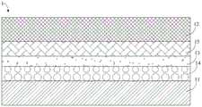
本申请实施例提供了一种发光器件,如图1所示,发光器件1包括阳极11、阴极12、发光层13以及空穴功能层14,其中,阳极11与阴极12相对设置,发光层13设置于阳极11与阴极12之间,空穴功能层14设置于阳极11与发光层13之间,其中,空穴功能层14的材料包括化合物A和化合物B,化合物A为聚(3,4-乙烯二氧噻吩):聚(苯乙烯磺酸盐)(PEDOT:PSS),化合物B具有下面通式(Ⅰ)所示的结构:The embodiment of the present application provides a light-emitting device. As shown in FIG. It is arranged between the

在通式(Ⅰ)中,R1和R2彼此独立地选自氢原子、包含碳原子数为1至10的烷基的基团、包含碳原子数为1至8的烷硫基的基团、包含碳原子数为1至8的烷氧基的基团、包含芳基的基团、包含芳氧基的基团、包含-CO-Rs的基团或包含-CO-O-Rt的基团,其中,Rs和Rt彼此独立地选自包含碳原子数为1至10的烷基的基团或包含芳基的基团;In the general formula (I), R1andR2 are independently selected from a hydrogen atom, a group containing an alkyl group having 1 to 10 carbon atoms, a group containing an alkylthio group having 1 to 8 carbon atoms group, a group containing an alkoxy group with a carbon number of 1 to 8, a group containing an aryl group, a group containing an aryloxy group, a group containing -CO-Rs or a group containing -CO-ORt A group, wherein Rs and Rt are independently selected from a group comprising an alkyl group having 1 to 10 carbon atoms or a group comprising an aryl group;
R3至R7彼此独立地选自氢原子、包含碳原子数为1至10的烷基的基团、包含碳原子数为1至8的烷硫基的基团、包含碳原子数为1至8的烷氧基的基团、氰基、硝基或卤素原子;R3 toR7 are independently selected from a hydrogen atom, a group containing an alkyl group with a carbon number of 1 to 10, a group containing an alkylthio group with a carbon number of 1 to 8, a group containing an alkylthio group with a carbon number of 1 to 8 alkoxy groups, cyano groups, nitro groups or halogen atoms;
R1至R7中的至少一者选自包含碳原子数为1至10的全氟烷基的基团。At least one of R1 to R7 is selected from groups containing a perfluoroalkyl group having 1 to 10 carbon atoms.
如本申请所用,“烷基”既包括未发生取代的烷基,又包括取代的烷基;“未发生取代的烷基”是指烷烃分子中失去一个氢原子而形成的脂肪烃基,包括直链的饱和脂肪烃基、支链的饱和脂肪烃基和成环的饱和脂肪烃基,烷基包括但不限于是于甲基、乙基、丙基、异丙基、正丁基、仲丁基、叔丁基、正戊基、仲戊基或环己基;“取代的烷基”是指脂肪烃基上的一个氢原子或多个氢原子任选地被其他基团取代而获得的基团,其他基团例如可以是卤素原子,允许存在多重取代度。As used in this application, "alkyl" includes both unsubstituted alkyl and substituted alkyl; "unsubstituted alkyl" refers to an aliphatic hydrocarbon group formed by losing a hydrogen atom in an alkane molecule, including straight Chain saturated aliphatic hydrocarbon group, branched chain saturated aliphatic hydrocarbon group and ring-forming saturated aliphatic hydrocarbon group, alkyl group includes but not limited to methyl, ethyl, propyl, isopropyl, n-butyl, sec-butyl, tert Butyl, n-pentyl, sec-pentyl or cyclohexyl; "substituted alkyl" refers to a group obtained by optionally replacing one or more hydrogen atoms on an aliphatic hydrocarbon group with other groups, and other groups A group can be, for example, a halogen atom, allowing for multiple degrees of substitution.
如本申请所用,“全氟烷基”是指对于烷烃分子中失去一个氢原子而形成的脂肪烃基,其上所有的氢原子全部由氟原子取代而获得基团。As used in this application, "perfluoroalkyl" refers to an aliphatic hydrocarbon group formed by losing one hydrogen atom in an alkane molecule, and all hydrogen atoms on it are replaced by fluorine atoms to obtain a group.
如本申请所用,“烷硫基”是指结构通式为Rx-S-的基团,其中,Rx表示烷基。As used in this application, "alkylthio" refers to a group with the general structural formula Rx -S-, wherein Rx represents an alkyl group.
如本申请所用,“烷氧基”是指结构通式为Rx-O-的基团,其中,Rx表示烷基。As used in this application, "alkoxy" refers to a group with the general structural formula Rx -O-, wherein Rx represents an alkyl group.
如本申请所用,“芳基”既包括未发生取代的芳基,又包括取代的芳基;“未发生取代的芳基”是指芳香环上仅包含碳原子的芳香基团,包括但不限于是苯基、1-萘基、2-萘基或联苯基;“取代的芳基”是指芳香环上仅包含碳原子的芳香基团上的一个氢原子或多个氢原子任选地被其他基团取代,其他基团例如可以是卤素原子或烷基,允许存在多重取代度。As used in this application, "aryl" includes both unsubstituted aryl and substituted aryl; "unsubstituted aryl" refers to an aromatic group containing only carbon atoms on the aromatic ring, including but not is limited to phenyl, 1-naphthyl, 2-naphthyl, or biphenyl; "substituted aryl" means a hydrogen atom or hydrogen atoms on an aromatic group containing only carbon atoms in the aromatic ring, optionally are substituted by other groups, such as halogen atoms or alkyl groups, allowing for multiple degrees of substitution.
如本申请所用,“芳氧基”是指结构通式为Ar-O-的基团,其中,Ar表示芳基。As used in this application, "aryloxy" refers to a group with the general structural formula Ar-O-, wherein Ar represents an aryl group.
在本申请的一些实施例中,在通式(Ⅰ)中,R1和R2彼此独立地选自包含碳原子数为3至6的环烷基的基团、包含碳原子数为1至10的全氟烷基的基团、包含苯基的基团、包含苯氧基的基团、包含-CO-Rs的基团或包含-CO-O-Rt的基团,其中,Rs选自碳原子数为1至10的卤代烷基、碳原子数为3至8的环烷基或苯基中的至少一者,Rt选自碳原子数为1至10的卤代烷基或苯基中的至少一者。In some embodiments of the present application, in the general formula (I), R1 and R2 are independently selected from a group comprising a cycloalkyl group with 3 to 6 carbon atoms, a group comprising a cycloalkyl group with 1 to 6
在本申请的一些实施例中,R1或R2选自包含全氟烷基的苯基。In some embodiments of the present application, R1 or R2 is selected from phenyl groups containing perfluoroalkyl groups.
在本申请的一示例中,R1选自包含一个或两个取代基的苯基,并且至少一个取代基包含全氟烷基,若取代基的数量超过两个,基于空间位阻较大的原因,化合物A与化合物B的适配组装程度有限。In an example of the present application, R1 is selected from phenyl groups containing one or two substituents, and at least one substituent contains perfluoroalkyl groups. If the number of substituents exceeds two, based on the larger steric hindrance The reason is that compound A and compound B have a limited degree of fit assembly.
在本申请的另一示例中,R2选自包含一个或两个取代基的苯基,并且至少一个取代基包含全氟烷基,若取代基的数量超过两个,基于空间位阻较大的原因,化合物A与化合物B的适配组装程度有限。In another example of the present application, Ris selected from phenyl containing one or two substituents, and at least one substituent contains a perfluoroalkyl group. The reason for the fit assembly of compound A and compound B is limited.
在本申请的一些实施例中,在通式(Ⅰ)中,R3至R7彼此独立地选自碳原子数为3至6的环烷基或碳原子数为1至10的全氟烷基中的至少一者。In some embodiments of the present application, in general formula (I), R3 to R7 are independently selected from cycloalkyl groups with 3 to 6 carbon atoms or perfluoroalkanes with 1 to 10 carbon atoms at least one of the bases.
在本申请的一些实施例中,R3至R7选自碳原子数为3至6的烷基,且R3至R7中的至少一者为碳原子数为1至4的全氟烷基。In some embodiments of the present application, R3 to R7 are selected from alkyl groups with 3 to 6 carbon atoms, and at least one of R3 to R7 is perfluoroalkane with 1 to 4 carbon atoms base.
在本申请的一些实施例中,化合物B选自:In some embodiments of the present application, compound B is selected from:


为了更易实现化合物A与化合物B的自组装,在本申请的一些实施例中,空穴功能层中化合物A:化合物B的质量比值为1:(1~10)。化合物B的含量过多或过少均对发光器件的性能改进效果有限。In order to realize the self-assembly of compound A and compound B more easily, in some embodiments of the present application, the mass ratio of compound A: compound B in the hole functional layer is 1: (1-10). Too much or too little content of Compound B has limited effect on improving the performance of the light-emitting device.
为了进一步地提高发光器件的综合性能,在本申请的一些实施例中,空穴功能层中化合物A:化合物B的质量比值为1:(5~8)。In order to further improve the overall performance of the light-emitting device, in some embodiments of the present application, the mass ratio of Compound A: Compound B in the hole functional layer is 1: (5-8).
在本申请的一些实施例中,阳极11和阴极12的材料彼此独立地选自金属、碳材料以及金属氧化物中的一种或多种,金属选自Al、Ag、Cu、Mo、Au、Ba、Ca以及Mg中的至少一种;碳材料选自石墨、碳纳米管、石墨烯以及碳纤维中的至少一种;金属氧化物可以是掺杂或非掺杂金属氧化物,选自ITO、FTO、ATO、AZO、GZO、IZO、MZO以及AMO中的至少一种。阳极11或阴极12也可以彼此独立地选自掺杂或非掺杂透明金属氧化物之间夹着金属的复合电极,复合电极包括但不限于是AZO/Ag/AZO、AZO/Al/AZO、ITO/Ag/ITO、ITO/Al/ITO、ZnO/Ag/ZnO、ZnO/Al/ZnO、TiO2/Ag/TiO2、TiO2/Al/TiO2、ZnS/Ag/ZnS、ZnS/Al/ZnS、TiO2/Ag/TiO2以及TiO2/Al/TiO2中的至少一种。阳极11的厚度例如可以是40nm至160nm,阴极12的厚度例如可以是20nm至120nm。In some embodiments of the present application, the materials of the
在本申请的一些实施例中,发光层13的材料包括有机发光材料或量子点,发光层13的厚度例如可以是10nm至30nm。In some embodiments of the present application, the material of the light-emitting
有机发光材料包括但不限于是二芳香基蒽衍生物、二苯乙烯芳香族衍生物、芘衍生物或芴衍生物、发蓝色光的TBPe荧光材料、发绿色光的TTPA荧光材料、发橙色光的TBRb荧光材料以及发红色光的DBP荧光材料中的至少一种。Organic luminescent materials include but are not limited to diaryl anthracene derivatives, stilbene aromatic derivatives, pyrene derivatives or fluorene derivatives, TBPe fluorescent materials emitting blue light, TTPA fluorescent materials emitting green light, orange light emitting At least one of the TBRb fluorescent material and the red-emitting DBP fluorescent material.
量子点可以红色量子点、绿色量子点以及蓝色量子点中的至少一种,量子点选自II-VI族化合物、III-V族化合物、IV-VI族化合物和I-III-VI族化合物中的至少一种,其中,I-VI族化合物选自CdS、CdSe、CdTe、ZnS、ZnSe、ZnTe、ZnO、HgS、HgSe、HgTe、CdSeS、CdSeTe、CdSTe、ZnSeS、ZnSeTe、ZnSTe、HgSeS、HgSeTe、HgSTe、CdZnS、CdZnSe、CdZnTe、CdHgS、CdHgSe、CdHgTe、HgZnS、HgZnSe、HgZnTe、CdZnSeS、CdZnSeTe、CdZnSTe、CdHgSeS、CdHgSeTe、CdHgSTe、HgZnSeS、HgZnSeTe以及HgZnSTe中的至少一种,III-V族化合物选自GaN、GaP、GaAs、GaSb、AlN、AlP、AlAs、AlSb、InN、InP、InAs、InSb、GaNP、GaNAs、GaNSb、GaPAs、GaPSb、AlNP、AlNAs、AlNSb、AlPAs、AlPSb、InNP、InNAs、InNSb、InPAs、InPSb、GaAlNP、GaAlNAs、GaAlNSb、GaAlPAs、GaAlPSb、GaInNP、GaInNAs、GaInNSb、GaInPAs、GaInPSb、InAlNP、InAlNAs、InAlNSb、InAlPAs以及InAlPSb中的至少一种,IV-VI族化合物选自SnS、SnSe、SnTe、PbS、PbSe、PbTe、SnSeS、SnSeTe、SnSTe、PbSeS、PbSeTe、PbSTe、SnPbS、SnPbSe、SnPbTe、SnPbSSe、SnPbSeTe以及SnPbSTe中的至少一种,I-III-VI族化合物选自CuInS2、CuInSe2和AgInS2中的至少一种。Quantum dots can be at least one of red quantum dots, green quantum dots and blue quantum dots, quantum dots are selected from II-VI group compounds, III-V group compounds, IV-VI group compounds and I-III-VI group compounds At least one of the group I-VI compounds selected from CdS, CdSe, CdTe, ZnS, ZnSe, ZnTe, ZnO, HgS, HgSe, HgTe, CdSeS, CdSeTe, CdSTe, ZnSeS, ZnSeTe, ZnSTe, HgSeS, HgSeTe , HgSTe, CdZnS, CdZnSe, CdZnTe, CdHgS, CdHgSe, CdHgTe, HgZnS, HgZnSe, HgZnTe, CdZnSeS, CdZnSeTe, CdZnSTe, CdHgSeS, CdHgSeTe, CdHgSTe, HgZnSeS, HgZnSeTe, and HgZnST At least one of e, III-V compound selected From GaN, GaP, GaAs, GaSb, AlN, AlP, AlAs, AlSb, InN, InP, InAs, InSb, GaNP, GaNAs, GaNSb, GaPAs, GaPSb, AlNP, AlNAs, AlNSb, AlPAs, AlPSb, InNP, InNAs, InNSb , InPAs, InPSb, GaAlNP, GaAlNAs, GaAlNSb, GaAlPAs, GaAlPSb, GaInNP, GaInNAs, GaInNSb, GaInPAs, GaInPSb, InAlNP, InAlNAs, InAlNSb, InAlPAs and InAlPSb at least one, the IV-VI group compound is selected from SnS, SnSe , SnTe, PbS, PbSe, PbTe, SnSeS, SnSeTe, SnSTe, PbSeS, PbSeTe, PbSTe, SnPbS, SnPbSe, SnPbTe, SnPbSSe, SnPbSeTe and SnPbSTe at least one, the I-III-VI group compound is selected from CuInS2 , At least one of CuInSe2 and AgInS2 .
在本申请的一些实施例中,如图2所示,在图1所示发光器件的基础上,发光器件1还包括电子传输层15,电子传输层15设置于发光层13与阴极12之间。电子传输层15的材料包括纳米金属氧化物,纳米金属氧化物既可以是未掺杂的纳米金属氧化物,也可以是掺杂的纳米金属氧化物,纳米金属氧化物例如选自ZnO、TiO2、SnO2、Ta2O3、ZrO2、TiLiO、ZnGaO、ZnAlO、ZnMgO、ZnSnO、ZnLiO、InSnO以及AlZnO中的至少一种。电子传输层15的厚度例如可以是10nm至60nm。In some embodiments of the present application, as shown in FIG. 2 , on the basis of the light-emitting device shown in FIG. 1 , the light-emitting
可以理解的是,本申请实施例的发光器件还可以包括其他层结构,例如发光器件还可以包括电子注入层,电子注入层设置于电子传输层与阴极之间,电子注入层的材料包括但不限于是碱金属卤化物、碱金属有机络合物以及有机膦化合物中的至少一种,碱金属卤化物包括但不限于是LiF,碱金属有机络合物包括但不限于是8-羟基喹啉锂,有机膦化合物包括但不限于是有机氧化磷、有机硫代膦化合物以及有机硒代膦化合物中的一种或多种。It can be understood that the light-emitting device in the embodiment of the present application may also include other layer structures, for example, the light-emitting device may also include an electron injection layer, the electron injection layer is arranged between the electron transport layer and the cathode, and the material of the electron injection layer includes but not Limited to at least one of alkali metal halides, alkali metal organic complexes and organic phosphine compounds, alkali metal halides include but not limited to LiF, alkali metal organic complexes include but not limited to 8-hydroxyquinoline Lithium, organic phosphine compounds include but not limited to one or more of organic phosphorus oxides, organic thiophosphine compounds and organic phosphine selenide compounds.
在本申请实施例的发光器件中,空穴功能层的材料包括化合物A和化合物B,由于化合物B的大π键与化合物A的PEDOT之间会产生基于非共价键的相互作用力而自组装形成稳定的有序结构,即:化合物A与化合物B之间凭借一种分散变化的电磁力来维系一定的空间结构,以自发地组织或聚集为一个稳定、具有一定规则几何外观的结构;此外,化合物B的表面能较低,使得化合物B会聚集于化合物A之上,相当于空穴功能层包含化合物A层和化合物B层两个层结构,其中,化合物A层相当于“空穴注入层”,化合物B层相当于“空穴传输层”。基于化合物A与化合物B自组装形成稳定的有序结构,因此,形成的化合物A层与化合物B层之间的势能壁垒较低,有效地提高了空穴注入,从而促进了空穴-电子传输平衡,进而提高了发光器件的发光效率,并降低了发光器件的工作电压,有利于延长发光器件的使用寿命。In the light-emitting device of the embodiment of the present application, the material of the hole functional layer includes compound A and compound B, because the large π bond of compound B and the PEDOT of compound A will generate a non-covalent bond-based interaction force and automatically Assembly to form a stable ordered structure, that is, compound A and compound B maintain a certain spatial structure by means of a dispersed and changing electromagnetic force, so as to spontaneously organize or aggregate into a stable structure with a certain regular geometric appearance; In addition, the surface energy of the compound B is low, so that the compound B will gather on the compound A, which is equivalent to the two-layer structure of the hole functional layer including the compound A layer and the compound B layer, wherein the compound A layer is equivalent to the "hole layer". Injection layer", compound B layer is equivalent to "hole transport layer". Based on the self-assembly of compound A and compound B to form a stable ordered structure, the potential energy barrier between the formed compound A layer and compound B layer is low, which effectively improves hole injection and thus promotes hole-electron transport balance, thereby improving the luminous efficiency of the light-emitting device, and reducing the operating voltage of the light-emitting device, which is beneficial to prolonging the service life of the light-emitting device.
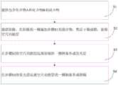
本申请实施例还提供了一种发光器件的制备方法,如图3所示,所述制备方法包括如下步骤:The embodiment of the present application also provides a method for preparing a light-emitting device, as shown in FIG. 3 , the method includes the following steps:
S1、提供包含化合物A和化合物B的混合物;S1, providing a mixture comprising compound A and compound B;
S2、提供阳极,在阳极的一侧施加步骤S1的混合物,然后干燥成膜,获得空穴功能层;S2, providing an anode, applying the mixture in step S1 to one side of the anode, and then drying to form a film to obtain a hole functional layer;
S3、在步骤S2的空穴功能层远离阳极的一侧制备形成发光层;S3, preparing and forming a light-emitting layer on the side of the hole functional layer away from the anode in step S2;
S4、在步骤S3的发光层远离空穴功能层的一侧制备形成阴极。S4. Prepare and form a cathode on the side of the light-emitting layer away from the hole functional layer in step S3.
或者,如图4所示,所述制备方法包括如下步骤:Or, as shown in Figure 4, the preparation method comprises the following steps:
S1’、提供阴极,在阴极的一侧制备形成发光层;S1', providing a cathode, preparing and forming a light-emitting layer on one side of the cathode;
S2’、提供包含化合物A和化合物B的混合物,在步骤S1’的阴极的一侧施加所述混合物,然后干燥成膜,获得空穴功能层;S2', providing a mixture comprising compound A and compound B, applying the mixture on one side of the cathode in step S1', and then drying to form a film to obtain a hole functional layer;
S3’、在步骤S2’的空穴功能层远离发光层的一侧制备形成阳极。S3', preparing and forming an anode on the side of the hole functional layer away from the light-emitting layer in step S2'.
在上述制备方法中,步骤S1至S4适用于制备正置型结构的发光器件,步骤S1’至S3’适用于制备倒置型结构的发光器件。化合物A为PEDOT:PSS,化合物B为通式(Ⅰ)所示结构的化合物。In the above preparation method, steps S1 to S4 are suitable for preparing a light-emitting device with an upright structure, and steps S1' to S3' are suitable for preparing a light-emitting device with an inverted structure. Compound A is PEDOT:PSS, and compound B is a compound with the structure shown in general formula (I).
在本申请的一些实施例中,混合物的施加方法为溶液法,溶液法包括但不限于是旋涂、涂布、喷墨打印、刮涂、浸渍提拉、浸泡、喷涂、滚涂或浇铸。“干燥成膜”是指所有能使湿膜获得更高能量而转变为干膜的操作,包括但不限于是热处理、静置自然晾干等,热处理既可以是恒温式热处理,也可以是非恒温式热处理(例如温度呈梯度式变化)。In some embodiments of the present application, the application method of the mixture is a solution method, and the solution method includes but is not limited to spin coating, coating, inkjet printing, blade coating, dipping, soaking, spraying, rolling or casting. "Drying to form a film" refers to all operations that can make the wet film obtain higher energy and convert it into a dry film, including but not limited to heat treatment, standing to dry naturally, etc. The heat treatment can be either constant temperature heat treatment or non-constant temperature Type heat treatment (for example, temperature gradient).
可以理解的是,发光器件的制备方法还可以包括其他膜层的制备步骤,例如在发光层与阴极之间制备电子传输层,又如在电子传输层与阴极之间制备电子注入层。It can be understood that the preparation method of the light-emitting device may also include preparation steps of other film layers, such as preparing an electron transport layer between the light-emitting layer and the cathode, or preparing an electron injection layer between the electron transport layer and the cathode.
需要说明的是,除了空穴功能层之外,发光器件中其他膜层的制备方法包括但不限于是溶液法和沉积法,沉积法包括化学法和物理法,化学法包括但不限于是化学气相沉积法、连续离子层吸附与反应法、阳极氧化法、电解沉积法或共沉淀法,物理法包括但不限于是热蒸发镀膜法、电子束蒸发镀膜法、磁控溅射法、多弧离子镀膜法、物理气相沉积法、原子层沉积法或脉冲激光沉积法。此外,若采用溶液法制备膜层,则需要对溶液法制得的湿膜进行干燥处理,以使湿膜转变为干膜。It should be noted that, in addition to the hole functional layer, the preparation methods of other film layers in light-emitting devices include but are not limited to solution methods and deposition methods. Deposition methods include chemical methods and physical methods. Chemical methods include but are not limited to chemical methods. Vapor deposition method, continuous ion layer adsorption and reaction method, anodic oxidation method, electrolytic deposition method or co-precipitation method, physical methods include but not limited to thermal evaporation coating method, electron beam evaporation coating method, magnetron sputtering method, multi-arc Ion coating, physical vapor deposition, atomic layer deposition or pulsed laser deposition. In addition, if the film layer is prepared by the solution method, the wet film prepared by the solution method needs to be dried to convert the wet film into a dry film.
本申请实施例还提供了一种显示装置,所述显示装置包括本申请实施例中任意一种所述的发光器件或者包括前面描述的制备方法制得的发光器件。所述显示装置可以是任何具有显示功能的电子产品,包括但不限于是智能手机、平板电脑、笔记本电脑、数码相机、数码摄像机、智能可穿戴设备、智能称重电子秤、车载显示器、电视机或电子书阅读器,其中,智能可穿戴设备例如可以是智能手环、智能手表、虚拟现实(Virtual Reality,VR)头盔等。The embodiment of the present application also provides a display device, the display device includes any one of the light-emitting device described in the embodiments of the present application or the light-emitting device manufactured by the preparation method described above. The display device can be any electronic product with a display function, including but not limited to smart phones, tablet computers, notebook computers, digital cameras, digital video cameras, smart wearable devices, smart weighing electronic scales, vehicle displays, televisions Or an e-book reader, wherein the smart wearable device may be, for example, a smart bracelet, a smart watch, a virtual reality (Virtual Reality, VR) helmet, and the like.
下面通过具体实施例、对比例和实验例对本申请的技术方案及技术效果进行详细说明,以下实施例仅仅是本申请的部分实施例,并非对本申请作出具体限定。The technical solutions and technical effects of the present application will be described in detail below through specific examples, comparative examples and experimental examples. The following examples are only part of the examples of the present application, and do not specifically limit the present application.
实施例1Example 1
本实施例提供了一种发光器件及其制备方法,所述发光器件为正置型结构的量子点发光二极管,如图5所示,在由下至上的方向上,发光器件1包括依次设置的衬底10、阳极11、空穴功能层14、发光层13、电子传输层15以及阴极12。This embodiment provides a light-emitting device and a preparation method thereof. The light-emitting device is a quantum dot light-emitting diode with an upright structure. As shown in FIG. 5 , in the direction from bottom to top, the light-emitting
发光器件1中各个层的材料与厚度分别为:The material and thickness of each layer in the
衬底10的材料为玻璃,厚度为2mm;The material of the
阳极11的材料为ITO,厚度为80nm;The material of the
阴极12的材料为Ag,厚度为100nm;The material of the
发光层13的材料为Cd0.10Zn0.9Se/Cd0.1Zn0.9Se/ZnSe/ZnS的量子点,发光波长为465nm,峰宽为21nm,厚度为25nm;The material of the light-emitting
空穴功能层14的材料由化合物A和化合物B组成,化合物A:化合物B的质量比值为1:1,空穴功能层14的厚度为35nm,其中,化合物A为PEDOT:PSS,化合物B具有如下式(1.1)所示的结构:The material of

电子传输层15的材料为粒径为4nm至6nm的纳米ZnO,厚度为30nm。The
本实施例中发光器件的制备方法包括如下步骤:The preparation method of the light-emitting device in this embodiment includes the following steps:
S1.1、提供衬底,在衬底的一侧蒸镀ITO以获得ITO层,然后将包含ITO的衬底依次采用丙酮超声清洗15min、清洁剂超声清洗15min、去离子水超声清洗15min以及异丙醇超声清洗15min,烘干后采用紫外-臭氧表面处理5min,获得包含阳极的衬底;S1.1. Provide a substrate, vapor-deposit ITO on one side of the substrate to obtain an ITO layer, and then ultrasonically clean the substrate containing ITO for 15 minutes with acetone, ultrasonic cleaning with detergent for 15 minutes, ultrasonic cleaning with deionized water for 15 minutes, and Ultrasonic cleaning with propanol for 15 minutes, followed by UV-ozone surface treatment for 5 minutes after drying, to obtain a substrate containing an anode;
S1.2、在常温常压的空气环境下,将化合物A(购自Baytron,产品型号为P-VP-AI4083)和化合物B(合成方法参照进行中国专利申请CN101878192A进行)按照化合物A:化合物B为1:1的质量比混合,获得混合物,在步骤S1.1的阳极远离衬底的一侧旋涂所述混合物,随后置于150℃下恒温热处理25min,获得空穴功能层;S1.2. In an air environment at normal temperature and pressure, compound A (purchased from Baytron, product model P-VP-AI4083) and compound B (the synthesis method is carried out with reference to Chinese patent application CN101878192A) according to compound A: compound B Mix at a mass ratio of 1:1 to obtain a mixture, spin-coat the mixture on the side of the anode away from the substrate in step S1.1, and then place it at 150°C for constant temperature heat treatment for 25 minutes to obtain a hole functional layer;
S1.3、在常温常压的氮气环境下,在步骤S1.2的空穴功能层远离阳极的一侧旋涂浓度为25mg/mL的Cd0.10Zn0.9Se/Cd0.1Zn0.9Se/ZnSe/ZnS量子点-正辛烷溶液,随后置于60℃下恒温热处理5min,获得发光层;S1.3. In a nitrogen environment at normal temperature and pressure, spin-coat Cd0.10 Zn 0.9 Se/Cd 0.1 Zn0.9 Se/ZnSe/Cd0.1 Zn0.9 Se/ZnSe/ ZnS quantum dot-n-octane solution, followed by heat treatment at 60°C for 5 minutes to obtain a light-emitting layer;
S1.4、在常温常压的氮气环境下,在步骤S1.3的发光层远离空穴功能层的一侧旋涂浓度为30mg/mL的纳米ZnO-乙醇溶液,然后置于80℃下热处理30min,获得电子传输层;S1.4. In a nitrogen environment at normal temperature and pressure, spin-coat a nano-ZnO-ethanol solution with a concentration of 30 mg/mL on the side of the light-emitting layer in step S1.3 away from the hole functional layer, and then heat-treat at 80°C 30min, obtain electron transport layer;
S1.5、在步骤S1.4的电子传输层远离发光层的一侧蒸镀Ag,获得阴极,然后封装获得发光器件。S1.5. Evaporate Ag on the side of the electron transport layer away from the light-emitting layer in step S1.4 to obtain a cathode, and then package to obtain a light-emitting device.
实施例2Example 2
本实施例提供了一种发光器件及其制备方法,相较于实施例1的发光器件,本实施例的发光器件的区别技术特征仅在于:在空穴功能层中,化合物A:化合物B的质量比值为1:4。This embodiment provides a light-emitting device and its preparation method. Compared with the light-emitting device in Example 1, the difference in technical features of the light-emitting device in this embodiment is only that: in the hole functional layer, compound A: compound B The mass ratio is 1:4.
相较于实施例1的制备方法,本实施例的制备方法的区别技术特征仅在于:将步骤S1.2替换为“在常温常压的空气环境下,将化合物A和化合物B按照化合物A:化合物B为1:4的质量比混合,获得混合物,在步骤S1.1的阳极远离衬底的一侧旋涂所述混合物,随后置于150℃下恒温热处理25min,获得空穴功能层”。Compared with the preparation method of Example 1, the difference technical feature of the preparation method of this example is only that: replace step S1.2 with "under normal temperature and pressure air environment, compound A and compound B according to compound A: Compound B was mixed at a mass ratio of 1:4 to obtain a mixture, which was spin-coated on the side of the anode away from the substrate in step S1.1, and then heat-treated at 150°C for 25 minutes to obtain a hole functional layer."
实施例3Example 3
本实施例提供了一种发光器件及其制备方法,相较于实施例1的发光器件,本实施例的发光器件的区别技术特征仅在于:在空穴功能层中,化合物A:化合物B的质量比值为1:5。This embodiment provides a light-emitting device and its preparation method. Compared with the light-emitting device in Example 1, the difference in technical features of the light-emitting device in this embodiment is only that: in the hole functional layer, compound A: compound B The mass ratio is 1:5.
相较于实施例1的制备方法,本实施例的制备方法的区别技术特征仅在于:将步骤S1.2替换为“在常温常压的空气环境下,将化合物A和化合物B按照化合物A:化合物B为1:5的质量比混合,获得混合物,在步骤S1.1的阳极远离衬底的一侧旋涂所述混合物,随后置于150℃下恒温热处理25min,获得空穴功能层”。Compared with the preparation method of Example 1, the difference technical feature of the preparation method of this example is only that: replace step S1.2 with "under normal temperature and pressure air environment, compound A and compound B according to compound A: Compound B was mixed at a mass ratio of 1:5 to obtain a mixture, which was spin-coated on the side of the anode away from the substrate in step S1.1, and then heat-treated at 150°C for 25 minutes to obtain a hole functional layer".
实施例4Example 4
本实施例提供了一种发光器件及其制备方法,相较于实施例1的发光器件,本实施例的发光器件的区别技术特征仅在于:在空穴功能层中,化合物A:化合物B的质量比值为1:5.5。This embodiment provides a light-emitting device and its preparation method. Compared with the light-emitting device in Example 1, the difference in technical features of the light-emitting device in this embodiment is only that: in the hole functional layer, compound A: compound B The mass ratio is 1:5.5.
相较于实施例1的制备方法,本实施例的制备方法的区别技术特征仅在于:将步骤S1.2替换为“在常温常压的空气环境下,将化合物A和化合物B按照化合物A:化合物B为1:5.5的质量比混合,获得混合物,在步骤S1.1的阳极远离衬底的一侧旋涂所述混合物,随后置于150℃下恒温热处理25min,获得空穴功能层”。Compared with the preparation method of Example 1, the difference technical feature of the preparation method of this example is only that: replace step S1.2 with "under normal temperature and pressure air environment, compound A and compound B according to compound A: Compound B was mixed at a mass ratio of 1:5.5 to obtain a mixture, which was spin-coated on the side of the anode away from the substrate in step S1.1, and then heat-treated at 150°C for 25 minutes to obtain a hole functional layer."
实施例5Example 5
本实施例提供了一种发光器件及其制备方法,相较于实施例1的发光器件,本实施例的发光器件的区别技术特征仅在于:在空穴功能层中,化合物A:化合物B的质量比值为1:6。This embodiment provides a light-emitting device and its preparation method. Compared with the light-emitting device in Example 1, the difference in technical features of the light-emitting device in this embodiment is only that: in the hole functional layer, compound A: compound B The mass ratio is 1:6.
相较于实施例1的制备方法,本实施例的制备方法的区别技术特征仅在于:将步骤S1.2替换为“在常温常压的空气环境下,将化合物A和化合物B按照化合物A:化合物B为1:6的质量比混合,获得混合物,在步骤S1.1的阳极远离衬底的一侧旋涂所述混合物,随后置于150℃下恒温热处理25min,获得空穴功能层”。Compared with the preparation method of Example 1, the difference technical feature of the preparation method of this example is only that: replace step S1.2 with "under normal temperature and pressure air environment, compound A and compound B according to compound A: Compound B was mixed at a mass ratio of 1:6 to obtain a mixture, and the mixture was spin-coated on the side of the anode away from the substrate in step S1.1, and then placed at 150°C for 25 minutes of constant temperature heat treatment to obtain a hole functional layer".
实施例6Example 6
本实施例提供了一种发光器件及其制备方法,相较于实施例1的发光器件,本实施例的发光器件的区别技术特征仅在于:在空穴功能层中,化合物A:化合物B的质量比值为1:8。This embodiment provides a light-emitting device and its preparation method. Compared with the light-emitting device in Example 1, the difference in technical features of the light-emitting device in this embodiment is only that: in the hole functional layer, compound A: compound B The mass ratio is 1:8.
相较于实施例1的制备方法,本实施例的制备方法的区别技术特征仅在于:将步骤S1.2替换为“在常温常压的空气环境下,将化合物A和化合物B按照化合物A:化合物B为1:8的质量比混合,获得混合物,在步骤S1.1的阳极远离衬底的一侧旋涂所述混合物,随后置于150℃下恒温热处理25min,获得空穴功能层”。Compared with the preparation method of Example 1, the difference technical feature of the preparation method of this example is only that: replace step S1.2 with "under normal temperature and pressure air environment, compound A and compound B according to compound A: Compound B was mixed at a mass ratio of 1:8 to obtain a mixture, which was spin-coated on the side of the anode away from the substrate in step S1.1, and then heat-treated at 150°C for 25 minutes to obtain a hole functional layer".
实施例7Example 7
本实施例提供了一种发光器件及其制备方法,相较于实施例1的发光器件,本实施例的发光器件的区别技术特征仅在于:在空穴功能层中,化合物A:化合物B的质量比值为1:10。This embodiment provides a light-emitting device and its preparation method. Compared with the light-emitting device in Example 1, the difference in technical features of the light-emitting device in this embodiment is only that: in the hole functional layer, compound A: compound B The mass ratio is 1:10.
相较于实施例1的制备方法,本实施例的制备方法的区别技术特征仅在于:将步骤S1.2替换为“在常温常压的空气环境下,将化合物A和化合物B按照化合物A:化合物B为1:10的质量比混合,获得混合物,在步骤S1.1的阳极远离衬底的一侧旋涂所述混合物,随后置于150℃下恒温热处理25min,获得空穴功能层”。Compared with the preparation method of Example 1, the difference technical feature of the preparation method of this example is only that: replace step S1.2 with "under normal temperature and pressure air environment, compound A and compound B according to compound A: Compound B was mixed at a mass ratio of 1:10 to obtain a mixture, which was spin-coated on the side of the anode away from the substrate in step S1.1, and then heat-treated at 150°C for 25 minutes to obtain a hole functional layer".
实施例8Example 8
本实施例提供了一种发光器件及其制备方法,相较于实施例1的发光器件,本实施例的发光器件的区别技术特征仅在于:在空穴功能层中,化合物A:化合物B的质量比值为1:5,且化合物B为具有下式(1.2)所示的结构:This embodiment provides a light-emitting device and its preparation method. Compared with the light-emitting device in Example 1, the difference in technical features of the light-emitting device in this embodiment is only that: in the hole functional layer, compound A: compound B The mass ratio is 1:5, and compound B has the structure shown in the following formula (1.2):

相较于实施例1的制备方法,本实施例的制备方法的区别技术特征仅在于:将步骤S1.2替换为“在常温常压的空气环境下,将化合物A和化合物B按照化合物A:化合物B为1:5的质量比混合,获得混合物,在步骤S1.1的阳极远离衬底的一侧旋涂所述混合物,随后置于150℃下恒温热处理25min,获得空穴功能层”。Compared with the preparation method of Example 1, the difference technical feature of the preparation method of this example is only that: replace step S1.2 with "under normal temperature and pressure air environment, compound A and compound B according to compound A: Compound B was mixed at a mass ratio of 1:5 to obtain a mixture, which was spin-coated on the side of the anode away from the substrate in step S1.1, and then heat-treated at 150°C for 25 minutes to obtain a hole functional layer".
实施例9Example 9
本实施例提供了一种发光器件及其制备方法,相较于实施例1的发光器件,本实施例的发光器件的区别技术特征仅在于:在空穴功能层中,化合物A:化合物B的质量比值为1:5.5,且化合物B为具有下式(1.3)所示的结构:This embodiment provides a light-emitting device and its preparation method. Compared with the light-emitting device in Example 1, the difference in technical features of the light-emitting device in this embodiment is only that: in the hole functional layer, compound A: compound B The mass ratio is 1:5.5, and compound B has the structure shown in the following formula (1.3):

相较于实施例1的制备方法,本实施例的制备方法的区别技术特征仅在于:将步骤S1.2替换为“在常温常压的空气环境下,将化合物A和化合物B按照化合物A:化合物B为1:5.5的质量比混合,获得混合物,在步骤S1.1的阳极远离衬底的一侧旋涂所述混合物,随后置于150℃下恒温热处理25min,获得空穴功能层”。Compared with the preparation method of Example 1, the difference technical feature of the preparation method of this example is only that: replace step S1.2 with "under normal temperature and pressure air environment, compound A and compound B according to compound A: Compound B was mixed at a mass ratio of 1:5.5 to obtain a mixture, which was spin-coated on the side of the anode away from the substrate in step S1.1, and then heat-treated at 150°C for 25 minutes to obtain a hole functional layer."
实施例10Example 10
本实施例提供了一种发光器件及其制备方法,相较于实施例1的发光器件,本实施例的发光器件的区别技术特征仅在于:在空穴功能层中,化合物A:化合物B的质量比值为1:5,且化合物B为具有下式(1.4)所示的结构:This embodiment provides a light-emitting device and its preparation method. Compared with the light-emitting device in Example 1, the difference in technical features of the light-emitting device in this embodiment is only that: in the hole functional layer, compound A: compound B The mass ratio is 1:5, and compound B has the structure shown in the following formula (1.4):

相较于实施例1的制备方法,本实施例的制备方法的区别技术特征仅在于:将步骤S1.2替换为“在常温常压的空气环境下,将化合物A和化合物B按照化合物A:化合物B为1:5的质量比混合,获得混合物,在步骤S1.1的阳极远离衬底的一侧旋涂所述混合物,随后置于150℃下恒温热处理25min,获得空穴功能层”。Compared with the preparation method of Example 1, the difference technical feature of the preparation method of this example is only that: replace step S1.2 with "under normal temperature and pressure air environment, compound A and compound B according to compound A: Compound B was mixed at a mass ratio of 1:5 to obtain a mixture, which was spin-coated on the side of the anode away from the substrate in step S1.1, and then heat-treated at 150°C for 25 minutes to obtain a hole functional layer".
实施例11Example 11
本实施例提供了一种发光器件及其制备方法,相较于实施例1的发光器件,本实施例的发光器件的区别技术特征仅在于:在空穴功能层中,化合物A:化合物B的质量比值为1:5.8,且化合物B为具有下式(1.5)所示的结构:This embodiment provides a light-emitting device and its preparation method. Compared with the light-emitting device in Example 1, the difference in technical features of the light-emitting device in this embodiment is only that: in the hole functional layer, compound A: compound B The mass ratio is 1:5.8, and compound B has the structure shown in the following formula (1.5):

相较于实施例1的制备方法,本实施例的制备方法的区别技术特征仅在于:将步骤S1.2替换为“在常温常压的空气环境下,将化合物A和化合物B按照化合物A:化合物B为1:5.8的质量比混合,获得混合物,在步骤S1.1的阳极远离衬底的一侧旋涂所述混合物,随后置于150℃下恒温热处理25min,获得空穴功能层”。Compared with the preparation method of Example 1, the difference technical feature of the preparation method of this example is only that: replace step S1.2 with "under normal temperature and pressure air environment, compound A and compound B according to compound A: Compound B was mixed at a mass ratio of 1:5.8 to obtain a mixture, which was spin-coated on the side of the anode away from the substrate in step S1.1, and then heat-treated at 150°C for 25 minutes to obtain a hole functional layer".
实施例12Example 12
本实施例提供了一种发光器件及其制备方法,相较于实施例1的发光器件,本实施例的发光器件的区别技术特征仅在于:在空穴功能层中,化合物A:化合物B的质量比值为1:5.6,且化合物B为具有下式(1.6)所示的结构:This embodiment provides a light-emitting device and its preparation method. Compared with the light-emitting device in Example 1, the difference in technical features of the light-emitting device in this embodiment is only that: in the hole functional layer, compound A: compound B The mass ratio is 1:5.6, and compound B has the structure shown in the following formula (1.6):

相较于实施例1的制备方法,本实施例的制备方法的区别技术特征仅在于:将步骤S1.2替换为“在常温常压的空气环境下,将化合物A和化合物B按照化合物A:化合物B为1:5.6的质量比混合,获得混合物,在步骤S1.1的阳极远离衬底的一侧旋涂所述混合物,随后置于150℃下恒温热处理25min,获得空穴功能层”。Compared with the preparation method of Example 1, the difference technical feature of the preparation method of this example is only that: replace step S1.2 with "under normal temperature and pressure air environment, compound A and compound B according to compound A: Compound B was mixed at a mass ratio of 1:5.6 to obtain a mixture, which was spin-coated on the side of the anode away from the substrate in step S1.1, and then heat-treated at 150°C for 25 minutes to obtain a hole functional layer."
对比例1Comparative example 1
本对比例提供了一种发光器件及其制备方法,相较于实施例1的发光器件,本对比例的发光器件的区别之处仅在于:空穴功能层的材料为化合物A(PEDOT:PSS)。This comparative example provides a light-emitting device and a preparation method thereof. Compared with the light-emitting device of Example 1, the difference between the light-emitting device of this comparative example is that the material of the hole functional layer is compound A (PEDOT:PSS ).
相较于实施例1的制备方法,本对比例的制备方法的区别之处仅在于:将步骤S1.2替换为“在常温常压的空气环境下,在步骤S1.1的阳极远离衬底的一侧旋涂化合物A,随后置于150℃下恒温热处理25min,获得空穴功能层”。Compared with the preparation method of Example 1, the only difference in the preparation method of this comparative example is that step S1.2 is replaced with "under normal temperature and pressure air environment, the anode in step S1.1 is far away from the substrate Spin-coat compound A on one side of the substrate, and then heat-treat at 150°C for 25 minutes to obtain a hole functional layer."
对比例2Comparative example 2
本对比例提供了一种发光器件及其制备方法,相较于实施例1的发光器件,本对比例的发光器件的区别之处仅在于:空穴功能层由层叠设置的空穴注入层和空穴传输层组成,其中,空穴注入层的材料为化合物A(PEDOT:PSS),空穴传输层的材料为聚(9,9-二辛基芴-CO-N-(4-丁基苯基)二苯胺)(简称为TFB,CAS号为220797-16-0),空穴注入层设置于阳极与发光层之间,空穴传输层设置于空穴注入层与发光层之间,其中,空穴注入层的厚度为20nm,空穴传输层的厚度为20nm。This comparative example provides a light-emitting device and a preparation method thereof. Compared with the light-emitting device of Example 1, the light-emitting device of this comparative example is only different in that: the hole functional layer is composed of a stacked hole injection layer and The hole transport layer is composed of, wherein, the material of the hole injection layer is compound A (PEDOT:PSS), and the material of the hole transport layer is poly(9,9-dioctylfluorene-CO-N-(4-butyl Phenyl)diphenylamine) (abbreviated as TFB, CAS No. 220797-16-0), the hole injection layer is arranged between the anode and the light emitting layer, and the hole transport layer is arranged between the hole injection layer and the light emitting layer, Wherein, the thickness of the hole injection layer is 20 nm, and the thickness of the hole transport layer is 20 nm.
相较于实施例1的制备方法,本对比例的制备方法的区别之处仅在于:将步骤S1.2替换为“在常温常压的空气环境下,在步骤S1.1的阳极远离衬底的一侧旋涂化合物A,随后置于150℃下恒温热处理30min,获得空穴注入层;然后,在空穴注入层远离阳极的一侧旋涂浓度为8mg/mL的TFB-氯苯溶液,随后置于180℃下恒温热处理30min,获得空穴传输层”。Compared with the preparation method of Example 1, the only difference in the preparation method of this comparative example is that step S1.2 is replaced with "under normal temperature and pressure air environment, the anode in step S1.1 is far away from the substrate One side of the hole injection layer was spin-coated with compound A, and then heat-treated at 150°C for 30 minutes to obtain a hole injection layer; then, a TFB-chlorobenzene solution with a concentration of 8 mg/mL was spin-coated on the side of the hole injection layer away from the anode, Then heat treatment at 180°C for 30 minutes at a constant temperature to obtain a hole transport layer".
实验例Experimental example
对实施例1至实施例12以及对比例1和对比例2的发光器件进行性能检测,检测项目包括:发光器件在2mA/cm2的电流密度下亮度由100%衰减至95%所需的时间(T95,h)和最大外量子效率(EQEmax,%),采用弗士达FPD光学特性测量设备(由LabView控制QE-PRO光谱仪、Keithley 2400以及Keithley 6485搭建的效率测试系统)测试获得各个发光器件的电压、电流、亮度、发光光谱等参数,并通过计算获得外量子点效率、功率效率等关键参数,并采用寿命测试设备测试获得各个发光器件的T95。The light-emitting devices of Examples 1 to 12 and Comparative Examples 1 and 2 were tested for performance, and the test items included: the time required for the brightness of the light-emitting device to decay from 100% to 95% at a current density of2mA /cm (T95,h) and the maximum external quantum efficiency (EQEmax ,%) were tested using FASTEC FPD optical characteristic measurement equipment (QE-PRO spectrometer controlled by LabView, efficiency test system built by Keithley 2400 and Keithley 6485) to obtain each luminescence Parameters such as voltage, current, brightness, and light-emitting spectrum of the device, and key parameters such as external quantum dot efficiency and power efficiency are obtained through calculation, and T95 of each light-emitting device is obtained by testing with life testing equipment.
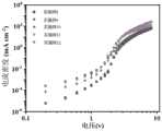
另外,测试实施例1至实施例12以及对比例1和对比例2的发光器件中空穴功能层的空穴迁移率/(×10-6cm2/V·s),进行空穴迁移率测试的结构器件由依次设置的阳极、空穴功能层、发光层和阴极(各个层的材料及厚度均参照对应的实施例和对比例,即相较于各个实施例、对比例1和对比例2的发光器件,此处进行空穴迁移率测试的结构器件仅省略了电子传输层),具体测试方法为:采用弗士达FPD光学特性测量设备测试相应的结构器件的电流密度-电压曲线(如图6和图7所示),获取电流密度-电压曲线中的空间电荷限制电流(SCLC)区,然后根据公式J=(9/8)εrε0μeV2/d3计算获得空穴迁移率,其中,J表示电流密度,单位为mA/cm2;εr表示相对介电常数;ε0表示真空介电常数;μe表示空穴迁移率,单位为cm2/V·s;V表示驱动电压,单位为V;d表示膜厚度,单位为m。需要说明的是,虽然进行空穴迁移率测试的结构器件并非为完整的发光器件,但是为了便于理解,图6和图7中仍以实施例1至实施例12以及对比例1和对比例2进行标识。In addition, the hole mobility/(×10-6 cm2 /V·s) of the hole functional layer in the light-emitting devices of Example 1 to Example 12 and Comparative Example 1 and Comparative Example 2 was tested, and the hole mobility test was carried out The structural device is composed of an anode, a hole functional layer, a light-emitting layer and a cathode arranged in sequence (the materials and thicknesses of each layer refer to the corresponding examples and comparative examples, that is, compared with each example, comparative example 1 and comparative example 2 The light-emitting device of the light-emitting device, the structural device for the hole mobility test here only omits the electron transport layer), the specific test method is: the current density-voltage curve (such as 6 and 7), obtain the space charge limited current (SCLC) region in the current density-voltage curve, and then calculate the space charge according to the formula J=(9/8)εr ε0 μe V2 /d3 Hole mobility, where J represents current density in mA/cm2 ; εr represents relative permittivity; ε0 represents vacuum permittivity; μe represents hole mobility in cm2 /V·s ; V represents the driving voltage, the unit is V; d represents the film thickness, the unit is m. It should be noted that although the structural device for the hole mobility test is not a complete light-emitting device, in order to facilitate understanding, Figures 6 and 7 are still represented by Examples 1 to 12 and Comparative Examples 1 and 2 To identify.
进一步地,测试实施例1至实施例12以及对比例1和对比例2的发光器件中电子传输层的电子迁移率,进行电子迁移率测试的结构器件由依次设置的阳极、发光层、电子传输层和阴极(各个层的材料及厚度均参照对应的实施例和对比例,即相较于各个实施例、对比例1和对比例2的发光器件,此处进行空穴迁移率测试的结构器件仅省略了空穴功能层),具体测试方法参照空穴迁移率的测试方法进行,需要说明的是,在此种测试方法下,测得的各个实施例、对比例1和对比例2的电子迁移率实际上是相同的,如图8所示,电子迁移率约为145.9×10⁻⁵cm2/V·s。Further, the electron mobility of the electron transport layer in the light-emitting devices of Examples 1 to 12 and Comparative Examples 1 and 2 was tested, and the structural device for the electron mobility test consists of an anode, a light-emitting layer, and an electron transport layer arranged in sequence. Layer and cathode (materials and thicknesses of each layer are referred to corresponding embodiments and comparative examples, that is, compared with the light-emitting devices of each embodiment, comparative example 1 and comparative example 2, the structural device for hole mobility testing here Only the hole functional layer is omitted), the specific test method is carried out with reference to the test method of hole mobility, it should be noted that, under this test method, the measured electron The mobility is practically the same, and as shown in Fig. 8, the electron mobility is about 145.9×10⁻⁵ cm2 /V·s.
性能测试结果详见下表1:The performance test results are detailed in Table 1 below:
表1实施例1至实施例12以及对比例1和对比例2的发光器件的性能检测结果Table 1 Performance test results of the light-emitting devices of Example 1 to Example 12 and Comparative Example 1 and Comparative Example 2

由表1、图6和图7可知,实施例1至实施例12的发光器件的综合性能具有明显的优势。以实施例4为例,实施例4中发光器件的空穴迁移率是对比例1中发光器件的空穴迁移率的3.3倍,且是对比例2中发光器件的空穴迁移率的2.1倍;实施例4中发光器件的EQEmax是对比例1中发光器件的EQEmax的6.7倍,且是对比例2中光器件的EQEmax的4.5倍;实施例4中发光器件的T95是对比例1中发光器件的T95的3.6倍,且是对比例2中光器件的T95的2.7倍。实施例1至实施例12的发光器件中电子迁移率与空穴迁移率之间的差值明显小于对比例1和对比例2的发光器件,其中,实施例4中发光器件的电子迁移率与空穴迁移率之间的差值最小,因此,实施例1至实施例12的发光器件的光电性能和使用寿命较对比例1和对比例2的发光器件更佳理想。It can be seen from Table 1, FIG. 6 and FIG. 7 that the overall performance of the light-emitting devices of Examples 1 to 12 has obvious advantages. Taking Example 4 as an example, the hole mobility of the light-emitting device in Example 4 is 3.3 times that of the light-emitting device in Comparative Example 1, and 2.1 times that of the light-emitting device in Comparative Example 2 The EQEmax of the light-emitting device in Example 4 is 6.7 times of the EQEmax of the light-emitting device in Comparative Example 1, and is 4.5 times of the EQEmax of the light-emitting device in Comparative Example 2; the T95 of the light-emitting device in Example 4 is the comparative example 3.6 times the T95 of the light-emitting device in 1, and 2.7 times the T95 of the light-emitting device in Comparative Example 2. The difference between electron mobility and hole mobility in the light-emitting devices of Examples 1 to 12 is significantly smaller than that of the light-emitting devices of Comparative Example 1 and Comparative Example 2, wherein the electron mobility of the light-emitting device in Example 4 and The difference between the hole mobility is the smallest, therefore, the photoelectric performance and service life of the light-emitting devices of Examples 1 to 12 are better than those of the light-emitting devices of Comparative Example 1 and Comparative Example 2.
本实验例的实验结果说明:采用化合物A和化合物B作为空穴功能层的材料,基于化合物A与化合物B会自组装形成稳定的有序结构,并且化合物A聚集于化合物B之上,因此,相当于空穴功能层包含化合物A层(等同于“空穴注入层”)和化合物B层(等同于“空穴传输层”)的两个层结构,形成的化合物A层与化合物B层之间的势能壁垒较低,有效地提高了空穴迁移率,从而促进了空穴-电子传输平衡,进而提高了发光器件的发光效率,有利于延长发光器件的使用寿命。此外,对比例2的空穴功能层是由层叠设置的空穴注入层和空穴传输层组成,在空穴功能层的制备方法中,需要依次制备空穴注入层和空穴传输层,不但增加了制程的繁琐程度和成本,而且空穴注入层与空穴传输层之间的势能壁垒较高,从而对空穴注入的促进效果有限,因此对比例2中发光器件的综合性能不如实施例1至实施例12的发光器件。The experimental results of this experimental example show that compound A and compound B are used as the material of the hole functional layer, based on the self-assembly of compound A and compound B to form a stable ordered structure, and compound A is aggregated on compound B, therefore, Equivalent to the two-layer structure of the hole functional layer including the compound A layer (equivalent to the "hole injection layer") and the compound B layer (equivalent to the "hole transport layer"), the formed compound A layer and the compound B layer The potential energy barrier between them is low, which effectively improves the hole mobility, thereby promoting the hole-electron transport balance, thereby improving the luminous efficiency of the light-emitting device, and is beneficial to prolonging the service life of the light-emitting device. In addition, the hole functional layer of Comparative Example 2 is composed of a stacked hole injection layer and a hole transport layer. In the preparation method of the hole functional layer, the hole injection layer and the hole transport layer need to be prepared sequentially. Not only The complexity and cost of the manufacturing process are increased, and the potential energy barrier between the hole injection layer and the hole transport layer is relatively high, so the promotion effect on hole injection is limited, so the overall performance of the light-emitting device in Comparative Example 2 is not as good as that of the
此外,在实施例1至实施例7的发光器件中,实施例3至实施例6的发光器件的综合性能优于实施例1、实施例2以及实施例7的发光器件,说明:当空穴功能层中化合物A:化合物B的质量比值为1:(5~8)时,化合物A和化合物B更易自组装形成稳定的有序结构,从而有利于进一步地提高发光器件的光电性能和使用寿命,In addition, among the light-emitting devices of Examples 1 to 7, the comprehensive performance of the light-emitting devices of Examples 3 to 6 is better than that of Examples 1, 2 and 7, indicating that when the holes function When the mass ratio of Compound A: Compound B in the layer is 1: (5-8), Compound A and Compound B are more likely to self-assemble to form a stable ordered structure, which is conducive to further improving the photoelectric performance and service life of the light-emitting device.
以上对本申请实施例所提供的一种发光器件、发光器件的制备方法以及显示装置,进行了详细介绍。本文中使用了具体个例对本申请的原理及实施方式进行了阐述,以上实施例的说明只是用于帮助理解本申请的技术方案及其核心思想;本领域的普通技术人员应当理解:其依然可以对前述各实施例所记载的技术方案进行修改,或者对其中部分技术特征进行等同替换;而这些修改或者替换,并不使相应技术方案的脱离本申请各实施例的技术方案的范围。A light-emitting device, a method for manufacturing the light-emitting device, and a display device provided in the embodiments of the present application have been described in detail above. This paper uses specific examples to illustrate the principles and implementation methods of the present application. The descriptions of the above embodiments are only used to help understand the technical solutions and core ideas of the present application; those of ordinary skill in the art should understand that: it can still Modifications are made to the technical solutions described in the foregoing embodiments, or equivalent replacements are made to some of the technical features; and these modifications or replacements do not make the corresponding technical solutions depart from the scope of the technical solutions of the various embodiments of the present application.
Claims (12)


Priority Applications (1)
| Application Number | Priority Date | Filing Date | Title |
|---|---|---|---|
| CN202111589623.3ACN116367578A (en) | 2021-12-23 | 2021-12-23 | Light emitting device, method of manufacturing the same, and display apparatus |
Applications Claiming Priority (1)
| Application Number | Priority Date | Filing Date | Title |
|---|---|---|---|
| CN202111589623.3ACN116367578A (en) | 2021-12-23 | 2021-12-23 | Light emitting device, method of manufacturing the same, and display apparatus |
Publications (1)
| Publication Number | Publication Date |
|---|---|
| CN116367578Atrue CN116367578A (en) | 2023-06-30 |
Family
ID=86935590
Family Applications (1)
| Application Number | Title | Priority Date | Filing Date |
|---|---|---|---|
| CN202111589623.3APendingCN116367578A (en) | 2021-12-23 | 2021-12-23 | Light emitting device, method of manufacturing the same, and display apparatus |
Country Status (1)
| Country | Link |
|---|---|
| CN (1) | CN116367578A (en) |
Citations (7)
| Publication number | Priority date | Publication date | Assignee | Title |
|---|---|---|---|---|
| US20050088080A1 (en)* | 2003-10-22 | 2005-04-28 | Hannstar Display Corporation | Organic light emitting diode |
| CN101878192A (en)* | 2008-03-31 | 2010-11-03 | 中央硝子株式会社 | Method for producing 4-perfluoroisopropylaniline |
| US20130015432A1 (en)* | 2011-07-14 | 2013-01-17 | Universal Display Corporation | Inorganic hosts in oleds |
| WO2013010661A1 (en)* | 2011-07-19 | 2013-01-24 | Heraeus Precious Metals Gmbh & Co. Kg. | Sam layers with an htl function |
| CN103928633A (en)* | 2013-01-16 | 2014-07-16 | 海洋王照明科技股份有限公司 | A kind of organic electroluminescence device and preparation method thereof |
| CN106784202A (en)* | 2017-02-28 | 2017-05-31 | Tcl集团股份有限公司 | QLED devices and preparation method thereof |
| CN109671853A (en)* | 2017-10-16 | 2019-04-23 | 乐金显示有限公司 | Light emitting diode and luminous display unit including light emitting diode |
- 2021
- 2021-12-23CNCN202111589623.3Apatent/CN116367578A/enactivePending
Patent Citations (8)
| Publication number | Priority date | Publication date | Assignee | Title |
|---|---|---|---|---|
| US20050088080A1 (en)* | 2003-10-22 | 2005-04-28 | Hannstar Display Corporation | Organic light emitting diode |
| CN101878192A (en)* | 2008-03-31 | 2010-11-03 | 中央硝子株式会社 | Method for producing 4-perfluoroisopropylaniline |
| US20130015432A1 (en)* | 2011-07-14 | 2013-01-17 | Universal Display Corporation | Inorganic hosts in oleds |
| WO2013010661A1 (en)* | 2011-07-19 | 2013-01-24 | Heraeus Precious Metals Gmbh & Co. Kg. | Sam layers with an htl function |
| TW201311862A (en)* | 2011-07-19 | 2013-03-16 | Heraeus Precious Metals Gmbh | SAM layer with HTL function |
| CN103928633A (en)* | 2013-01-16 | 2014-07-16 | 海洋王照明科技股份有限公司 | A kind of organic electroluminescence device and preparation method thereof |
| CN106784202A (en)* | 2017-02-28 | 2017-05-31 | Tcl集团股份有限公司 | QLED devices and preparation method thereof |
| CN109671853A (en)* | 2017-10-16 | 2019-04-23 | 乐金显示有限公司 | Light emitting diode and luminous display unit including light emitting diode |
Similar Documents
| Publication | Publication Date | Title |
|---|---|---|
| CN116987298A (en) | Thin film, light emitting device and display device | |
| CN118870848A (en) | Optoelectronic device and method for manufacturing the same, and display device | |
| CN116367578A (en) | Light emitting device, method of manufacturing the same, and display apparatus | |
| US20250221156A1 (en) | Photoelectric device, and preparation method thereof | |
| CN116156919A (en) | Light-emitting device, manufacturing method thereof, and display device | |
| CN117693210A (en) | Photoelectric device, preparation method of photoelectric device and electronic equipment | |
| CN116437686A (en) | Light emitting device, manufacturing method of light emitting device and display device | |
| CN116234405A (en) | Light emitting device, manufacturing method of light emitting device and display device | |
| CN117222244A (en) | Composite material, film, light-emitting device and display device | |
| WO2023116207A1 (en) | Composition, preparation method for composition, and light-emitting device | |
| CN116669451A (en) | Light emitting device and display device including light emitting device | |
| WO2024213140A1 (en) | Light-emitting device, manufacturing method for light-emitting device, and display apparatus | |
| CN117693213A (en) | Photoelectric device, preparation method of photoelectric device and electronic equipment | |
| CN116156920A (en) | Light emitting device, manufacturing method of light emitting device and display device | |
| CN116437690A (en) | Preparation method of light-emitting device, light-emitting device and display device | |
| CN118695645A (en) | Photoelectric device, method for preparing photoelectric device, and electronic device | |
| CN116367583A (en) | Light emitting device, manufacturing method of light emitting device and display device | |
| WO2024093747A1 (en) | Composite material, preparation method for the composite material, and photoelectric device containing the composite material | |
| CN116425711A (en) | Compound, light-emitting device, preparation method of light-emitting device and display device | |
| WO2023197658A1 (en) | Light-emitting device, preparation method for light-emitting device, and display apparatus | |
| CN117651462A (en) | Method for preparing film, photoelectric device and electronic equipment | |
| CN119012741A (en) | Photoelectric device, preparation method thereof and display device | |
| CN117645280A (en) | Preparation method of composite material, light-emitting device and display device | |
| CN117430092A (en) | Composite material, preparation method of composite material, photoelectric device and electronic equipment | |
| CN116981311A (en) | Preparation method of light-emitting device, light-emitting device and display device |
Legal Events
| Date | Code | Title | Description |
|---|---|---|---|
| PB01 | Publication | ||
| PB01 | Publication | ||
| SE01 | Entry into force of request for substantive examination | ||
| SE01 | Entry into force of request for substantive examination |