CN116364010A - Sub-pixel circuit, display panel and display device - Google Patents
Sub-pixel circuit, display panel and display deviceDownload PDFInfo
- Publication number
- CN116364010A CN116364010ACN202211232709.5ACN202211232709ACN116364010ACN 116364010 ACN116364010 ACN 116364010ACN 202211232709 ACN202211232709 ACN 202211232709ACN 116364010 ACN116364010 ACN 116364010A
- Authority
- CN
- China
- Prior art keywords
- voltage
- circuit
- transistor
- driving
- light emitting
- Prior art date
- Legal status (The legal status is an assumption and is not a legal conclusion. Google has not performed a legal analysis and makes no representation as to the accuracy of the status listed.)
- Granted
Links
Images


Classifications
- G—PHYSICS
- G09—EDUCATION; CRYPTOGRAPHY; DISPLAY; ADVERTISING; SEALS
- G09G—ARRANGEMENTS OR CIRCUITS FOR CONTROL OF INDICATING DEVICES USING STATIC MEANS TO PRESENT VARIABLE INFORMATION
- G09G3/00—Control arrangements or circuits, of interest only in connection with visual indicators other than cathode-ray tubes
- G09G3/20—Control arrangements or circuits, of interest only in connection with visual indicators other than cathode-ray tubes for presentation of an assembly of a number of characters, e.g. a page, by composing the assembly by combination of individual elements arranged in a matrix no fixed position being assigned to or needed to be assigned to the individual characters or partial characters
- G09G3/2007—Display of intermediate tones
- G09G3/2074—Display of intermediate tones using sub-pixels
- G—PHYSICS
- G09—EDUCATION; CRYPTOGRAPHY; DISPLAY; ADVERTISING; SEALS
- G09G—ARRANGEMENTS OR CIRCUITS FOR CONTROL OF INDICATING DEVICES USING STATIC MEANS TO PRESENT VARIABLE INFORMATION
- G09G3/00—Control arrangements or circuits, of interest only in connection with visual indicators other than cathode-ray tubes
- G09G3/20—Control arrangements or circuits, of interest only in connection with visual indicators other than cathode-ray tubes for presentation of an assembly of a number of characters, e.g. a page, by composing the assembly by combination of individual elements arranged in a matrix no fixed position being assigned to or needed to be assigned to the individual characters or partial characters
- G09G3/22—Control arrangements or circuits, of interest only in connection with visual indicators other than cathode-ray tubes for presentation of an assembly of a number of characters, e.g. a page, by composing the assembly by combination of individual elements arranged in a matrix no fixed position being assigned to or needed to be assigned to the individual characters or partial characters using controlled light sources
- G09G3/30—Control arrangements or circuits, of interest only in connection with visual indicators other than cathode-ray tubes for presentation of an assembly of a number of characters, e.g. a page, by composing the assembly by combination of individual elements arranged in a matrix no fixed position being assigned to or needed to be assigned to the individual characters or partial characters using controlled light sources using electroluminescent panels
- G09G3/32—Control arrangements or circuits, of interest only in connection with visual indicators other than cathode-ray tubes for presentation of an assembly of a number of characters, e.g. a page, by composing the assembly by combination of individual elements arranged in a matrix no fixed position being assigned to or needed to be assigned to the individual characters or partial characters using controlled light sources using electroluminescent panels semiconductive, e.g. using light-emitting diodes [LED]
- G09G3/3208—Control arrangements or circuits, of interest only in connection with visual indicators other than cathode-ray tubes for presentation of an assembly of a number of characters, e.g. a page, by composing the assembly by combination of individual elements arranged in a matrix no fixed position being assigned to or needed to be assigned to the individual characters or partial characters using controlled light sources using electroluminescent panels semiconductive, e.g. using light-emitting diodes [LED] organic, e.g. using organic light-emitting diodes [OLED]
- G09G3/3225—Control arrangements or circuits, of interest only in connection with visual indicators other than cathode-ray tubes for presentation of an assembly of a number of characters, e.g. a page, by composing the assembly by combination of individual elements arranged in a matrix no fixed position being assigned to or needed to be assigned to the individual characters or partial characters using controlled light sources using electroluminescent panels semiconductive, e.g. using light-emitting diodes [LED] organic, e.g. using organic light-emitting diodes [OLED] using an active matrix
- G09G3/3233—Control arrangements or circuits, of interest only in connection with visual indicators other than cathode-ray tubes for presentation of an assembly of a number of characters, e.g. a page, by composing the assembly by combination of individual elements arranged in a matrix no fixed position being assigned to or needed to be assigned to the individual characters or partial characters using controlled light sources using electroluminescent panels semiconductive, e.g. using light-emitting diodes [LED] organic, e.g. using organic light-emitting diodes [OLED] using an active matrix with pixel circuitry controlling the current through the light-emitting element
- G—PHYSICS
- G09—EDUCATION; CRYPTOGRAPHY; DISPLAY; ADVERTISING; SEALS
- G09G—ARRANGEMENTS OR CIRCUITS FOR CONTROL OF INDICATING DEVICES USING STATIC MEANS TO PRESENT VARIABLE INFORMATION
- G09G3/00—Control arrangements or circuits, of interest only in connection with visual indicators other than cathode-ray tubes
- G09G3/20—Control arrangements or circuits, of interest only in connection with visual indicators other than cathode-ray tubes for presentation of an assembly of a number of characters, e.g. a page, by composing the assembly by combination of individual elements arranged in a matrix no fixed position being assigned to or needed to be assigned to the individual characters or partial characters
- G09G3/22—Control arrangements or circuits, of interest only in connection with visual indicators other than cathode-ray tubes for presentation of an assembly of a number of characters, e.g. a page, by composing the assembly by combination of individual elements arranged in a matrix no fixed position being assigned to or needed to be assigned to the individual characters or partial characters using controlled light sources
- G09G3/28—Control arrangements or circuits, of interest only in connection with visual indicators other than cathode-ray tubes for presentation of an assembly of a number of characters, e.g. a page, by composing the assembly by combination of individual elements arranged in a matrix no fixed position being assigned to or needed to be assigned to the individual characters or partial characters using controlled light sources using luminous gas-discharge panels, e.g. plasma panels
- G—PHYSICS
- G09—EDUCATION; CRYPTOGRAPHY; DISPLAY; ADVERTISING; SEALS
- G09G—ARRANGEMENTS OR CIRCUITS FOR CONTROL OF INDICATING DEVICES USING STATIC MEANS TO PRESENT VARIABLE INFORMATION
- G09G3/00—Control arrangements or circuits, of interest only in connection with visual indicators other than cathode-ray tubes
- G09G3/20—Control arrangements or circuits, of interest only in connection with visual indicators other than cathode-ray tubes for presentation of an assembly of a number of characters, e.g. a page, by composing the assembly by combination of individual elements arranged in a matrix no fixed position being assigned to or needed to be assigned to the individual characters or partial characters
- G09G3/22—Control arrangements or circuits, of interest only in connection with visual indicators other than cathode-ray tubes for presentation of an assembly of a number of characters, e.g. a page, by composing the assembly by combination of individual elements arranged in a matrix no fixed position being assigned to or needed to be assigned to the individual characters or partial characters using controlled light sources
- G09G3/30—Control arrangements or circuits, of interest only in connection with visual indicators other than cathode-ray tubes for presentation of an assembly of a number of characters, e.g. a page, by composing the assembly by combination of individual elements arranged in a matrix no fixed position being assigned to or needed to be assigned to the individual characters or partial characters using controlled light sources using electroluminescent panels
- G09G3/32—Control arrangements or circuits, of interest only in connection with visual indicators other than cathode-ray tubes for presentation of an assembly of a number of characters, e.g. a page, by composing the assembly by combination of individual elements arranged in a matrix no fixed position being assigned to or needed to be assigned to the individual characters or partial characters using controlled light sources using electroluminescent panels semiconductive, e.g. using light-emitting diodes [LED]
- G09G3/3208—Control arrangements or circuits, of interest only in connection with visual indicators other than cathode-ray tubes for presentation of an assembly of a number of characters, e.g. a page, by composing the assembly by combination of individual elements arranged in a matrix no fixed position being assigned to or needed to be assigned to the individual characters or partial characters using controlled light sources using electroluminescent panels semiconductive, e.g. using light-emitting diodes [LED] organic, e.g. using organic light-emitting diodes [OLED]
- G09G3/3266—Details of drivers for scan electrodes
- G—PHYSICS
- G09—EDUCATION; CRYPTOGRAPHY; DISPLAY; ADVERTISING; SEALS
- G09G—ARRANGEMENTS OR CIRCUITS FOR CONTROL OF INDICATING DEVICES USING STATIC MEANS TO PRESENT VARIABLE INFORMATION
- G09G3/00—Control arrangements or circuits, of interest only in connection with visual indicators other than cathode-ray tubes
- G09G3/20—Control arrangements or circuits, of interest only in connection with visual indicators other than cathode-ray tubes for presentation of an assembly of a number of characters, e.g. a page, by composing the assembly by combination of individual elements arranged in a matrix no fixed position being assigned to or needed to be assigned to the individual characters or partial characters
- G09G3/22—Control arrangements or circuits, of interest only in connection with visual indicators other than cathode-ray tubes for presentation of an assembly of a number of characters, e.g. a page, by composing the assembly by combination of individual elements arranged in a matrix no fixed position being assigned to or needed to be assigned to the individual characters or partial characters using controlled light sources
- G09G3/30—Control arrangements or circuits, of interest only in connection with visual indicators other than cathode-ray tubes for presentation of an assembly of a number of characters, e.g. a page, by composing the assembly by combination of individual elements arranged in a matrix no fixed position being assigned to or needed to be assigned to the individual characters or partial characters using controlled light sources using electroluminescent panels
- G09G3/32—Control arrangements or circuits, of interest only in connection with visual indicators other than cathode-ray tubes for presentation of an assembly of a number of characters, e.g. a page, by composing the assembly by combination of individual elements arranged in a matrix no fixed position being assigned to or needed to be assigned to the individual characters or partial characters using controlled light sources using electroluminescent panels semiconductive, e.g. using light-emitting diodes [LED]
- G09G3/3208—Control arrangements or circuits, of interest only in connection with visual indicators other than cathode-ray tubes for presentation of an assembly of a number of characters, e.g. a page, by composing the assembly by combination of individual elements arranged in a matrix no fixed position being assigned to or needed to be assigned to the individual characters or partial characters using controlled light sources using electroluminescent panels semiconductive, e.g. using light-emitting diodes [LED] organic, e.g. using organic light-emitting diodes [OLED]
- G09G3/3275—Details of drivers for data electrodes
- G09G3/3291—Details of drivers for data electrodes in which the data driver supplies a variable data voltage for setting the current through, or the voltage across, the light-emitting elements
- G—PHYSICS
- G09—EDUCATION; CRYPTOGRAPHY; DISPLAY; ADVERTISING; SEALS
- G09G—ARRANGEMENTS OR CIRCUITS FOR CONTROL OF INDICATING DEVICES USING STATIC MEANS TO PRESENT VARIABLE INFORMATION
- G09G3/00—Control arrangements or circuits, of interest only in connection with visual indicators other than cathode-ray tubes
- G09G3/20—Control arrangements or circuits, of interest only in connection with visual indicators other than cathode-ray tubes for presentation of an assembly of a number of characters, e.g. a page, by composing the assembly by combination of individual elements arranged in a matrix no fixed position being assigned to or needed to be assigned to the individual characters or partial characters
- G09G3/34—Control arrangements or circuits, of interest only in connection with visual indicators other than cathode-ray tubes for presentation of an assembly of a number of characters, e.g. a page, by composing the assembly by combination of individual elements arranged in a matrix no fixed position being assigned to or needed to be assigned to the individual characters or partial characters by control of light from an independent source
- G09G3/36—Control arrangements or circuits, of interest only in connection with visual indicators other than cathode-ray tubes for presentation of an assembly of a number of characters, e.g. a page, by composing the assembly by combination of individual elements arranged in a matrix no fixed position being assigned to or needed to be assigned to the individual characters or partial characters by control of light from an independent source using liquid crystals
- G09G3/3611—Control of matrices with row and column drivers
- G09G3/3648—Control of matrices with row and column drivers using an active matrix
- G—PHYSICS
- G09—EDUCATION; CRYPTOGRAPHY; DISPLAY; ADVERTISING; SEALS
- G09G—ARRANGEMENTS OR CIRCUITS FOR CONTROL OF INDICATING DEVICES USING STATIC MEANS TO PRESENT VARIABLE INFORMATION
- G09G3/00—Control arrangements or circuits, of interest only in connection with visual indicators other than cathode-ray tubes
- G09G3/20—Control arrangements or circuits, of interest only in connection with visual indicators other than cathode-ray tubes for presentation of an assembly of a number of characters, e.g. a page, by composing the assembly by combination of individual elements arranged in a matrix no fixed position being assigned to or needed to be assigned to the individual characters or partial characters
- G09G3/34—Control arrangements or circuits, of interest only in connection with visual indicators other than cathode-ray tubes for presentation of an assembly of a number of characters, e.g. a page, by composing the assembly by combination of individual elements arranged in a matrix no fixed position being assigned to or needed to be assigned to the individual characters or partial characters by control of light from an independent source
- G09G3/36—Control arrangements or circuits, of interest only in connection with visual indicators other than cathode-ray tubes for presentation of an assembly of a number of characters, e.g. a page, by composing the assembly by combination of individual elements arranged in a matrix no fixed position being assigned to or needed to be assigned to the individual characters or partial characters by control of light from an independent source using liquid crystals
- G09G3/3611—Control of matrices with row and column drivers
- G09G3/3674—Details of drivers for scan electrodes
- G—PHYSICS
- G09—EDUCATION; CRYPTOGRAPHY; DISPLAY; ADVERTISING; SEALS
- G09G—ARRANGEMENTS OR CIRCUITS FOR CONTROL OF INDICATING DEVICES USING STATIC MEANS TO PRESENT VARIABLE INFORMATION
- G09G3/00—Control arrangements or circuits, of interest only in connection with visual indicators other than cathode-ray tubes
- G09G3/20—Control arrangements or circuits, of interest only in connection with visual indicators other than cathode-ray tubes for presentation of an assembly of a number of characters, e.g. a page, by composing the assembly by combination of individual elements arranged in a matrix no fixed position being assigned to or needed to be assigned to the individual characters or partial characters
- G09G3/34—Control arrangements or circuits, of interest only in connection with visual indicators other than cathode-ray tubes for presentation of an assembly of a number of characters, e.g. a page, by composing the assembly by combination of individual elements arranged in a matrix no fixed position being assigned to or needed to be assigned to the individual characters or partial characters by control of light from an independent source
- G09G3/36—Control arrangements or circuits, of interest only in connection with visual indicators other than cathode-ray tubes for presentation of an assembly of a number of characters, e.g. a page, by composing the assembly by combination of individual elements arranged in a matrix no fixed position being assigned to or needed to be assigned to the individual characters or partial characters by control of light from an independent source using liquid crystals
- G09G3/3611—Control of matrices with row and column drivers
- G09G3/3685—Details of drivers for data electrodes
- G—PHYSICS
- G09—EDUCATION; CRYPTOGRAPHY; DISPLAY; ADVERTISING; SEALS
- G09G—ARRANGEMENTS OR CIRCUITS FOR CONTROL OF INDICATING DEVICES USING STATIC MEANS TO PRESENT VARIABLE INFORMATION
- G09G2300/00—Aspects of the constitution of display devices
- G09G2300/08—Active matrix structure, i.e. with use of active elements, inclusive of non-linear two terminal elements, in the pixels together with light emitting or modulating elements
- G09G2300/0809—Several active elements per pixel in active matrix panels
- G09G2300/0819—Several active elements per pixel in active matrix panels used for counteracting undesired variations, e.g. feedback or autozeroing
- G—PHYSICS
- G09—EDUCATION; CRYPTOGRAPHY; DISPLAY; ADVERTISING; SEALS
- G09G—ARRANGEMENTS OR CIRCUITS FOR CONTROL OF INDICATING DEVICES USING STATIC MEANS TO PRESENT VARIABLE INFORMATION
- G09G2300/00—Aspects of the constitution of display devices
- G09G2300/08—Active matrix structure, i.e. with use of active elements, inclusive of non-linear two terminal elements, in the pixels together with light emitting or modulating elements
- G09G2300/0809—Several active elements per pixel in active matrix panels
- G09G2300/0842—Several active elements per pixel in active matrix panels forming a memory circuit, e.g. a dynamic memory with one capacitor
- G09G2300/0852—Several active elements per pixel in active matrix panels forming a memory circuit, e.g. a dynamic memory with one capacitor being a dynamic memory with more than one capacitor
- G—PHYSICS
- G09—EDUCATION; CRYPTOGRAPHY; DISPLAY; ADVERTISING; SEALS
- G09G—ARRANGEMENTS OR CIRCUITS FOR CONTROL OF INDICATING DEVICES USING STATIC MEANS TO PRESENT VARIABLE INFORMATION
- G09G2310/00—Command of the display device
- G09G2310/02—Addressing, scanning or driving the display screen or processing steps related thereto
- G09G2310/0264—Details of driving circuits
- G09G2310/0278—Details of driving circuits arranged to drive both scan and data electrodes
- G—PHYSICS
- G09—EDUCATION; CRYPTOGRAPHY; DISPLAY; ADVERTISING; SEALS
- G09G—ARRANGEMENTS OR CIRCUITS FOR CONTROL OF INDICATING DEVICES USING STATIC MEANS TO PRESENT VARIABLE INFORMATION
- G09G2310/00—Command of the display device
- G09G2310/02—Addressing, scanning or driving the display screen or processing steps related thereto
- G09G2310/0264—Details of driving circuits
- G09G2310/0291—Details of output amplifiers or buffers arranged for use in a driving circuit
- G—PHYSICS
- G09—EDUCATION; CRYPTOGRAPHY; DISPLAY; ADVERTISING; SEALS
- G09G—ARRANGEMENTS OR CIRCUITS FOR CONTROL OF INDICATING DEVICES USING STATIC MEANS TO PRESENT VARIABLE INFORMATION
- G09G2310/00—Command of the display device
- G09G2310/08—Details of timing specific for flat panels, other than clock recovery
- G—PHYSICS
- G09—EDUCATION; CRYPTOGRAPHY; DISPLAY; ADVERTISING; SEALS
- G09G—ARRANGEMENTS OR CIRCUITS FOR CONTROL OF INDICATING DEVICES USING STATIC MEANS TO PRESENT VARIABLE INFORMATION
- G09G2320/00—Control of display operating conditions
- G09G2320/02—Improving the quality of display appearance
- G09G2320/0233—Improving the luminance or brightness uniformity across the screen
- G—PHYSICS
- G09—EDUCATION; CRYPTOGRAPHY; DISPLAY; ADVERTISING; SEALS
- G09G—ARRANGEMENTS OR CIRCUITS FOR CONTROL OF INDICATING DEVICES USING STATIC MEANS TO PRESENT VARIABLE INFORMATION
- G09G2320/00—Control of display operating conditions
- G09G2320/02—Improving the quality of display appearance
- G09G2320/029—Improving the quality of display appearance by monitoring one or more pixels in the display panel, e.g. by monitoring a fixed reference pixel
- G09G2320/0295—Improving the quality of display appearance by monitoring one or more pixels in the display panel, e.g. by monitoring a fixed reference pixel by monitoring each display pixel
- G—PHYSICS
- G09—EDUCATION; CRYPTOGRAPHY; DISPLAY; ADVERTISING; SEALS
- G09G—ARRANGEMENTS OR CIRCUITS FOR CONTROL OF INDICATING DEVICES USING STATIC MEANS TO PRESENT VARIABLE INFORMATION
- G09G2320/00—Control of display operating conditions
- G09G2320/04—Maintaining the quality of display appearance
- G09G2320/041—Temperature compensation
- G—PHYSICS
- G09—EDUCATION; CRYPTOGRAPHY; DISPLAY; ADVERTISING; SEALS
- G09G—ARRANGEMENTS OR CIRCUITS FOR CONTROL OF INDICATING DEVICES USING STATIC MEANS TO PRESENT VARIABLE INFORMATION
- G09G2320/00—Control of display operating conditions
- G09G2320/04—Maintaining the quality of display appearance
- G09G2320/043—Preventing or counteracting the effects of ageing
Landscapes
- Engineering & Computer Science (AREA)
- Physics & Mathematics (AREA)
- Computer Hardware Design (AREA)
- General Physics & Mathematics (AREA)
- Theoretical Computer Science (AREA)
- Chemical & Material Sciences (AREA)
- Crystallography & Structural Chemistry (AREA)
- Plasma & Fusion (AREA)
- Control Of Indicators Other Than Cathode Ray Tubes (AREA)
- Control Of El Displays (AREA)
Abstract
Translated fromChinese
Description
Translated fromChinese相关申请的交叉引用Cross References to Related Applications
本申请要求于2021年12月20日提交的韩国专利申请第10-2021-0182406号的优先权,该韩国专利申请出于所有目的通过引用合并于此,就如同在本文中完全阐述的一样。This application claims priority from Korean Patent Application No. 10-2021-0182406 filed on December 20, 2021, which is hereby incorporated by reference for all purposes as if fully set forth herein.
技术领域technical field
本公开内容的实施方式涉及子像素电路、显示面板和显示装置。Embodiments of the present disclosure relate to sub-pixel circuits, display panels, and display devices.
背景技术Background technique
基于数字数据来显示图像的代表性显示装置包括使用液晶的液晶显示(LCD)装置和使用有机发光二极管(OLED)的有机发光显示装置。Representative display devices that display images based on digital data include liquid crystal display (LCD) devices using liquid crystals and organic light emitting display devices using organic light emitting diodes (OLEDs).
在这些显示装置中,有机发光二极管显示器采用有机发光二极管,因此具有快速响应能力,并在对比度、发光效率、亮度以及视角方面具有各种优点。在这种情况下,发光二极管可以用无机材料或有机材料来实现。Among these display devices, organic light emitting diode displays employ organic light emitting diodes, and thus have fast response capability, and have various advantages in terms of contrast, luminous efficiency, brightness, and viewing angle. In this case, light-emitting diodes can be realized with inorganic or organic materials.
有机发光二极管显示器包括布置在显示面板上的子像素中的发光二极管,并且通过控制流向发光二极管的电流使发光二极管发光,从而在显示图像时控制由每个子像素表示的亮度。The organic light emitting diode display includes light emitting diodes arranged in subpixels on a display panel, and the light emitting diodes are made to emit light by controlling current flowing to the light emitting diodes, thereby controlling brightness represented by each subpixel when displaying an image.
这样的显示装置可以具有设置在显示面板上以驱动发光元件的子像素电路。例如,子像素电路包括用于控制流经发光元件的驱动电流的驱动晶体管、以及用于根据扫描信号控制驱动晶体管的栅极-源极电压的至少一个扫描晶体管。子像素电路的扫描晶体管可以由从设置在显示面板的基板上的栅极驱动电路输出的扫描信号控制。Such a display device may have sub-pixel circuits provided on a display panel to drive light emitting elements. For example, the sub-pixel circuit includes a driving transistor for controlling a driving current flowing through a light emitting element, and at least one scanning transistor for controlling a gate-source voltage of the driving transistor according to a scanning signal. The scan transistor of the sub-pixel circuit may be controlled by a scan signal output from a gate driving circuit provided on a substrate of the display panel.
在这种情况下,诸如构成每个子像素的驱动晶体管的阈值电压或迁移率之类的特性值会根据驱动时间而变化,或者每个晶体管的特性值可能由于每个子像素的驱动时间的差异而发生偏差。可能会引起子像素之间的亮度的偏差(亮度不均匀),从而降低图像质量。In this case, characteristic values such as the threshold voltage or mobility of the driving transistors constituting each sub-pixel may vary depending on the driving time, or the characteristic values of each transistor may change due to differences in the driving time of each sub-pixel Deviation occurs. Variation in luminance (non-uniformity in luminance) among sub-pixels may be caused, thereby degrading image quality.
为了解决子像素之间的亮度的偏差,显示装置已经采用了用于感测子像素的特性值(例如,驱动晶体管的阈值电压或迁移率)并对该子像素的特性值进行补偿的技术。To address variations in luminance between subpixels, display devices have employed techniques for sensing and compensating for characteristic values of subpixels (eg, threshold voltage or mobility of driving transistors).
然而,由于构成子像素的发光元件也可能根据显示装置的使用时间而劣化,因此难以同时补偿发光元件的劣化和驱动晶体管的特性值。However, since the light emitting elements constituting the sub-pixels may also degrade depending on the usage time of the display device, it is difficult to simultaneously compensate the deterioration of the light emitting elements and the characteristic values of the driving transistors.
发明内容Contents of the invention
本公开内容的发明人发明了能够同时补偿驱动晶体管的劣化和发光元件的劣化的子像素电路、显示面板和显示装置。因此,本公开内容的实施方式涉及基本上消除由于相关技术的限制和缺点而引起的一个或更多个问题的子像素电路、显示面板和显示装置。The inventors of the present disclosure have invented a sub-pixel circuit, a display panel, and a display device capable of simultaneously compensating for degradation of a driving transistor and degradation of a light emitting element. Accordingly, embodiments of the present disclosure are directed to a sub-pixel circuit, a display panel, and a display device that substantially obviate one or more problems due to limitations and disadvantages of the related art.
本公开内容的实施方式可以提供能够同时补偿驱动晶体管的劣化和发光元件的劣化的子像素电路、显示面板和显示装置。Embodiments of the present disclosure may provide a sub-pixel circuit, a display panel, and a display device capable of simultaneously compensating for degradation of a driving transistor and degradation of a light emitting element.
本公开内容的实施方式可以提供能够通过控制流经发光元件的驱动电流与数据电压成比例来同时补偿驱动晶体管的劣化和发光元件的劣化的子像素电路、显示面板和显示装置。Embodiments of the present disclosure may provide a sub-pixel circuit, a display panel, and a display device capable of simultaneously compensating for degradation of a driving transistor and degradation of a light emitting element by controlling a driving current flowing through the light emitting element in proportion to a data voltage.
本公开内容的实施方式可以提供无论驱动晶体管的特性值的变化如何,流经发光元件的驱动电流都被控制为与数据电压成比例的子像素电路、显示面板和显示装置。Embodiments of the present disclosure may provide a sub-pixel circuit, a display panel, and a display device in which a driving current flowing through a light emitting element is controlled to be proportional to a data voltage regardless of a variation in a characteristic value of a driving transistor.
另外的特征和方面将部分地在随后的描述中阐述,并且部分地将从描述中变得明显,或者可以通过实践本文提供的发明构思而获知。本发明构思的其他特征和方面可以通过在撰写的说明书、其权利要求和附图中特别指出或者可推导出的结构来实现和获得。Additional features and aspects will be set forth in part in the description which follows and, in part, will be obvious from the description, or may be learned by practice of the inventive concepts presented herein. The other features and aspects of the inventive concept may be realized and obtained by means of the structure particularly pointed out or inferred from the written description, claims hereof and the appended drawings.
为了实现本发明构思的这些和其他方面,如本文中实施和广泛描述的那样,用于操作设置在显示面板上的多个子像素中的至少一个子像素的子像素电路可以包括:参考电路,其被配置成接收高电位电压并且输出用于控制流经发光元件的驱动电流的控制电压;发光电路,其包括发光元件,发光电路被配置成接收控制电压和低电位电压,并且基于驱动电压控制发光元件;放大电路,其被配置成将控制电压与数据电压进行比较以生成用于控制发光电路的驱动电压;以及输入电路,其被配置成接收数据电压和第一扫描信号,并且基于第一扫描信号控制将数据电压施加至放大电路的时序。To achieve these and other aspects of the inventive concept, as embodied and broadly described herein, a subpixel circuit for operating at least one of a plurality of subpixels disposed on a display panel may include a reference circuit that configured to receive a high-potential voltage and output a control voltage for controlling a driving current flowing through a light-emitting element; a light-emitting circuit including a light-emitting element configured to receive the control voltage and a low-potential voltage, and control light emission based on the driving voltage element; an amplification circuit configured to compare the control voltage with a data voltage to generate a drive voltage for controlling the light emitting circuit; and an input circuit configured to receive the data voltage and the first scan signal, and The signal controls the timing of applying the data voltage to the amplifying circuit.
在另一个方面中,显示面板可以包括多个子像素和以上详述的子像素电路。In another aspect, a display panel may include a plurality of subpixels and the subpixel circuitry detailed above.
在又一个方面中,显示装置可以包括:显示面板,其包括多个子像素和用于操作多个子像素中的至少一个子像素的子像素电路;栅极驱动电路,其被配置成通过多个栅极线分别向显示面板供应多个扫描信号;数据驱动电路,其被配置成通过多个数据线分别向显示面板供应多个数据电压;以及时序控制器,其被配置成驱动栅极驱动电路和数据驱动电路。在此,子像素电路可以包括:参考电路,其被配置成接收高电位电压并且输出用于控制流经发光元件的驱动电流的控制电压;发光电路,其包括发光元件,发光电路被配置成接收控制电压和低电位电压,并且基于驱动电压控制发光元件;放大电路,其被配置成将控制电压与数据电压进行比较以生成用于控制发光电路的驱动电压;以及输入电路,其被配置成接收数据电压和第一扫描信号,并且基于第一扫描信号控制将数据电压施加至放大电路的时序。In yet another aspect, a display device may include: a display panel including a plurality of sub-pixels and a sub-pixel circuit for operating at least one of the plurality of sub-pixels; a gate driving circuit configured to the pole lines respectively supply a plurality of scan signals to the display panel; the data driving circuit configured to respectively supply a plurality of data voltages to the display panel through the plurality of data lines; and a timing controller configured to drive the gate driving circuit and data drive circuit. Here, the sub-pixel circuit may include: a reference circuit configured to receive a high potential voltage and output a control voltage for controlling a driving current flowing through the light emitting element; a light emitting circuit including a light emitting element configured to receive a control voltage and a low-potential voltage, and control a light emitting element based on the driving voltage; an amplification circuit configured to compare the control voltage with a data voltage to generate a driving voltage for controlling the light emitting circuit; and an input circuit configured to receive The data voltage and the first scan signal, and the timing of applying the data voltage to the amplifying circuit is controlled based on the first scan signal.
根据本公开内容的实施方式,可以提供能够同时补偿驱动晶体管的劣化和发光元件的劣化的子像素电路、显示面板和显示装置。According to embodiments of the present disclosure, it is possible to provide a sub-pixel circuit, a display panel, and a display device capable of simultaneously compensating for degradation of a driving transistor and degradation of a light emitting element.
根据本公开内容的实施方式,可以提供能够通过控制流经发光元件的驱动电流与数据电压成比例来同时补偿驱动晶体管的劣化和发光元件的劣化的子像素电路、显示面板和显示装置。According to embodiments of the present disclosure, there may be provided a sub-pixel circuit, a display panel, and a display device capable of simultaneously compensating for degradation of a driving transistor and degradation of a light emitting element by controlling a driving current flowing through the light emitting element in proportion to a data voltage.
根据本公开内容的实施方式,可以提供无论驱动晶体管的特性值的变化如何,流经发光元件的驱动电流都被控制为与数据电压成比例的子像素电路、显示面板和显示装置。According to embodiments of the present disclosure, it is possible to provide a sub-pixel circuit, a display panel, and a display device in which a driving current flowing through a light emitting element is controlled to be proportional to a data voltage regardless of a variation in a characteristic value of a driving transistor.
应当理解,本公开内容的上述一般描述和以下详细描述都是示例性和解释性的,旨在提供对所要求保护的发明构思的进一步解释。It is to be understood that both the foregoing general description and the following detailed description of the present disclosure are exemplary and explanatory and are intended to provide further explanation of the claimed inventive concept.
附图说明Description of drawings
被包括以提供对本公开内容的进一步理解并且被并入本说明书中并构成本说明书的一部分的附图示出了本公开内容的实施方式,并且与说明书一起用于说明本公开内容的原理。在附图中:The accompanying drawings, which are included to provide a further understanding of the disclosure and are incorporated in and constitute a part of this specification, illustrate embodiments of the disclosure and together with the description serve to explain the principles of the disclosure. In the attached picture:
图1是示意性地示出根据本公开内容的各种示例实施方式的显示装置的配置的图;FIG. 1 is a diagram schematically illustrating a configuration of a display device according to various example embodiments of the present disclosure;
图2是示出根据本公开内容的示例实施方式的显示装置的系统的示例的图;FIG. 2 is a diagram illustrating an example of a system of a display device according to an example embodiment of the present disclosure;
图3是示出显示装置的子像素电路的示例的图。FIG. 3 is a diagram illustrating an example of a sub-pixel circuit of a display device.
图4是示出对显示装置中的驱动晶体管的阈值电压进行外部补偿的示例的信号时序图;4 is a signal timing diagram illustrating an example of externally compensating a threshold voltage of a driving transistor in a display device;
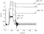
图5是示出对显示装置中的驱动晶体管的迁移率进行外部补偿的示例的信号时序图;5 is a signal timing diagram illustrating an example of externally compensating the mobility of a driving transistor in a display device;
图6是示出对显示装置中的驱动晶体管的阈值电压和迁移率进行内部补偿的示例的信号时序图;6 is a signal timing diagram illustrating an example of internally compensating for a threshold voltage and a mobility of a driving transistor in a display device;
图7是示出根据本公开内容的示例实施方式的子像素电路的框图;7 is a block diagram illustrating a sub-pixel circuit according to an example embodiment of the present disclosure;
图8是示出根据本公开内容的示例实施方式的子像素电路的详细配置的图;8 is a diagram illustrating a detailed configuration of a sub-pixel circuit according to an example embodiment of the present disclosure;
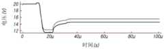
图9是示出根据本公开内容的示例实施方式的子像素电路的操作的示例信号波形图;FIG. 9 is an example signal waveform diagram illustrating an operation of a sub-pixel circuit according to an example embodiment of the present disclosure;
图10是示出根据本公开内容的示例实施方式的流经参考电路的电流根据子像素电路中的数据电压而变化的信号波形图;10 is a signal waveform diagram illustrating a change in current flowing through a reference circuit according to a data voltage in a sub-pixel circuit according to an example embodiment of the present disclosure;
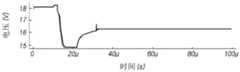
图11A、图11B和图11C是示出根据本公开内容的示例实施方式的当驱动晶体管在子像素电路中具有不同阈值电压时子像素电路的电流和电压变化的信号波形图;11A, 11B, and 11C are signal waveform diagrams illustrating current and voltage changes of sub-pixel circuits when driving transistors have different threshold voltages in the sub-pixel circuits according to example embodiments of the present disclosure;
图12是示出根据本公开内容的示例实施方式的另一子像素电路的详细配置的图;以及12 is a diagram showing a detailed configuration of another sub-pixel circuit according to an example embodiment of the present disclosure; and
图13是示出根据本公开内容的示例实施方式的另一子像素电路的操作的示例信号波形图。FIG. 13 is an example signal waveform diagram illustrating an operation of another sub-pixel circuit according to an example embodiment of the present disclosure.
具体实施方式Detailed ways
将通过参照附图描述的以下示例实施方式阐明本公开内容的优点和特征及其实现方法。然而,本公开内容可以以不同的形式来实施,并且不应被解释为限于本文阐述的示例实施方式。而是,提供这些示例实施方案以便使本公开内容可以足够彻底和完整,以帮助本领域技术人员完全理解本公开内容的范围。此外,本公开内容的保护范围由权利要求及其等同物限定。Advantages and features of the present disclosure and methods of achieving them will be clarified through the following example embodiments described with reference to the accompanying drawings. This disclosure may, however, be embodied in different forms and should not be construed as limited to the example embodiments set forth herein. Rather, these example embodiments are provided so that this disclosure will be thorough and complete enough to help those skilled in the art fully understand the scope of the disclosure. Furthermore, the protection scope of the present disclosure is defined by the claims and their equivalents.
除非另有说明,否则相同的附图标记始终表示相同的元件。在下面的说明中使用的各个元件的名称仅是为了方便书写说明书而选择的,并且因此可以与实际产品中使用的名称不同。Unless otherwise stated, the same reference numerals denote the same elements throughout. The names of the respective elements used in the following description are selected only for the convenience of writing the specification, and thus may be different from the names used in actual products.
在以下描述中,在相关已知功能或配置的详细描述可能不必要地混淆本公开内容的示例实施方式的一个方面的情况下,可以省略对这种已知配置功能的详细描述。In the following description, where a detailed description of a related known function or configuration may unnecessarily obscure an aspect of the example embodiments of the present disclosure, a detailed description of such a known configuration function may be omitted.
在使用术语“包括(comprise)”、“具有”、“包括(include)”、“包含(contain)”、“构成”、“由……组成”、“由……形成”等的情况下,可以添加一个或更多个其他元素,除非这些术语与更具限制性的术语例如“仅”一起使用。以单数形式描述的元素旨在包括复数形式,反之,以复数形式描述的元素旨在包括单数形式除非上下文另有明确说明。Where the terms "comprise", "have", "include", "contain", "consist of", "consist of", "formed of", etc. are used, One or more other elements may be added, unless these terms are used with a more restrictive term such as "only". Elements described in the singular are intended to include the plural, whereas elements described in the plural are intended to include the singular unless the context clearly dictates otherwise.
尽管在本文中可以使用术语“第一”、“第二”、A、B、(a)、(b)等来描述各种元素,但是这些元素不应被解释为受这些术语的限制,因为这些术语不用于限定特定的顺序或优先级。这些术语仅用于区分一个元件和另一个元件。例如,在没有脱离本公开内容的范围的情况下,第一元件可以被称为第二元件,并且类似地,第二元件可以被称为第一元件。Although the terms "first", "second", A, B, (a), (b), etc. may be used herein to describe various elements, these elements should not be construed as being limited by these terms because These terms are not intended to define a specific order or priority. These terms are only used to distinguish one element from another. For example, a first element could be termed a second element, and, similarly, a second element could be termed a first element, without departing from the scope of the present disclosure.
在使用元件或层“连接至”、“耦合至”、“粘附至”另一个元件或层或者与另一个元件或层“接触”、“交叠”的表述的情况下,除非另有说明,否则该元件或层不仅能够直接连接、耦合或粘附至另一个元件或层或者与另一个元件或层直接“接触”、“交叠”,而且能够通过“设置”或“插入”在元素或层之间的一个或更多个中间元件或层间接连接、耦合或粘附至另一个元件或层或者与另一个元件或层间接“接触”、“交叠”。Where the expression that an element or layer is "connected to," "coupled to," "adhered to," or "in contact with," or "overlaps" another element or layer is used, unless otherwise stated , otherwise the element or layer can not only be directly connected, coupled or adhered to another element or layer or directly "contact" or "overlap" another element or layer, but also can One or more intermediate elements or layers between or layers are indirectly connected, coupled, or adhered to, or indirectly "contact", "overlap" another element or layer.
在过程、操作、流程、步骤、事件等之间的时间关系被描述为例如“之后”、“随后”、“下一个”或“之前”的情况下,该关系不仅涵盖连续或顺序的次序,而且还可以涵盖非连续或非顺序的关系,除非使用了更具限制性的术语,例如“正好”、“紧”或“直接”。Where a temporal relationship between procedures, operations, flows, steps, events, etc. is described as, for example, "after", "sequent", "next" or "before", the relationship does not encompass only a sequential or sequential order, Also, non-sequential or non-sequential relationships are contemplated, unless more restrictive terms such as "exactly," "tightly," or "directly" are used.
在附图中示出以描述本公开内容的各种示例实施方式的形状、尺寸、比率、角度、数目等仅作为示例给出。因此,本公开内容不限于附图中的说明。The shapes, dimensions, ratios, angles, numbers, etc. shown in the drawings to describe various example embodiments of the present disclosure are given by way of example only. Therefore, the present disclosure is not limited to the description in the drawings.
在解释元件时,即使在没有提供这种误差或公差范围的明确描述的情况下,元件(包括其尺寸和相对尺寸)也将被解释为包括普通误差或公差范围。公差或误差范围可能由各种因素引起,例如工艺因素、内部或外部影响、噪声等。此外,术语“可以”完全包含术语“能够”的所有含义。In interpreting elements, even in the absence of an explicit description of such error or tolerance ranges, elements (including their dimensions and relative dimensions) will be construed as including ordinary error or tolerance ranges. The tolerance or margin of error may be caused by various factors, such as process factors, internal or external influences, noise, etc. Furthermore, the term "may" fully encompasses all meanings of the term "capable of".
现在将详细参照本公开内容的实施方式,其示例可以在附图中示出。Reference will now be made in detail to embodiments of the present disclosure, examples of which may be illustrated in the accompanying drawings.
图1是示意性地示出根据本公开内容的各种示例实施方式的显示装置的配置的图。FIG. 1 is a diagram schematically illustrating a configuration of a display device according to various example embodiments of the present disclosure.
如图1所示,根据本公开内容的示例实施方式的显示装置100可以包括显示面板110,在显示面板110中连接有多个栅极线GL和数据线DL,并且以矩阵形式布置有多个子像素SP。显示装置100还可以包括用于驱动多个栅极线GL的栅极驱动电路120、用于通过多个数据线DL供应数据电压的数据驱动电路130、用于控制栅极驱动电路120和数据驱动电路130的时序控制器140以及电力管理电路150。As shown in FIG. 1 , a
显示面板110基于通过多个栅极线GL从栅极驱动电路120传递的扫描信号和通过多个数据线DL从数据驱动电路130传递的数据电压来显示图像。The
在液晶显示器的情况下,显示面板110可以包括形成在两个基板之间的液晶层,并且可以以诸如扭曲向列(TN)模式、垂直对准(VA)模式、平面内切换(IPS)模式或边缘场切换(FFS)模式的任何已知模式进行操作。在有机发光显示器的情况下,显示面板110可以以顶部发射方案、底部发射方案或双发射方案来实现。In the case of a liquid crystal display, the
在显示面板110中,多个像素可以以矩阵形式被布置。每个像素可以包括具有不同颜色的子像素SP例如白色子像素、红色子像素、绿色子像素和蓝色子像素。子像素SP可以由多个数据线DL和多个栅极线GL分别限定。In the
一个子像素SP可以包括例如形成在一个数据线DL与一个栅极线GL之间的交叉点处的薄膜晶体管(TFT)、用数据电压充电的诸如有机发光二极管的发光元件、以及电连接至发光元件以维持电压的存储电容器。One sub-pixel SP may include, for example, a thin film transistor (TFT) formed at an intersection between one data line DL and one gate line GL, a light emitting element such as an organic light emitting diode charged with a data voltage, and a light emitting element electrically connected to a light emitting diode. element to maintain the voltage of the storage capacitor.
例如,如果具有2160×3840分辨率的显示装置100包括白色(W)、红色(R)、绿色(G)和蓝色(B)四个子像素SP,则3840个数据线DL可以分别连接至2160个栅极线GL和四个子像素WRGB。因此,可以在显示装置100中设置3840×4=15360个数据线DL。每个子像素SP可以设置在对应栅极线GL与对应数据线DL之间的交叉点处。For example, if a
栅极驱动电路120可以由时序控制器140控制以将扫描信号顺序地输出至设置在显示面板110中的多个栅极线GL,从而控制多个子像素SP的驱动时序。The
在分辨率为例如2160×3840的显示装置100中,将扫描信号顺序地输出至从第一栅极线至第2160栅极线的2160个栅极线GL可以被称为2160相位驱动。将扫描信号顺序地输出至四个栅极线GL的每个单元,例如在将扫描信号顺序地输出至第一个栅极线至第四个栅极线之后将扫描信号顺序地输出至第五个栅极线至第八个栅极线,这被称为为4相驱动方法。换言之,将扫描信号顺序地输出至每N个栅极线GL可以被称为N相驱动。In the
栅极驱动电路120可以包括一个或更多个栅极驱动集成电路(GDIC)。根据要实现的驱动方案,栅极驱动电路120可以位于显示面板110的仅一侧或两个相对侧中的每一侧上。栅极驱动电路120可以以将其嵌入显示面板110的边框区域中的面板内栅极(GIP)形式实现。The
数据驱动电路130可以从时序控制器140接收图像数据DATA,并将接收到的图像数据DATA转换成模拟数据电压。然后,随着可以根据施加至对应栅极线GL的扫描信号的时序将数据电压输出至每个数据线DL,连接至数据线DL的每个子像素SP可以显示具有与数据电压对应的亮度的发光信号。The
同样,数据驱动电路130可以包括一个或更多个源极驱动集成电路SDIC。源极驱动集成电路SDIC可以以带自动键合(TAB,Tape Automated Bonding)型或玻璃上芯片(COG,Chip On Glass)型连接至显示面板110的键合焊盘,或者直接设置在显示面板110上。Also, the
在一些情况下,每个源极驱动集成电路SDIC可以集成并设置在显示面板110上。此外,每个源极驱动器集成电路SDIC可以以膜上芯片(COF)类型实现。在这种情况下,每个源极驱动器集成电路SDIC可以安装在电路膜上,并且可以通过电路膜电连接至显示面板110的对应数据线DL。In some cases, each source driver integrated circuit SDIC may be integrated and disposed on the
时序控制器140可以向栅极驱动电路120和数据驱动电路130提供各种控制信号,并且可以控制栅极驱动电路120和数据驱动电路130的操作。换言之,时序控制器140可以控制栅极驱动电路120,以根据在每帧中实现的时序输出扫描信号,而另一方面,可以将从外部装置(例如,经由主机系统200)接收的图像数据DATA传递至数据驱动电路130。The
在这种情况下,时序控制器140从外部主机系统200接收若干时序信号连同图像数据DATA,时序信号包括例如垂直同步信号Vsync、水平同步信号Hsync、数据使能信号DE和主时钟MCLK。In this case, the
主机系统200可以是电视(TV)系统、机顶盒、导航系统、个人计算机(PC)、家庭影院系统、移动装置和可穿戴式装置中的任何一种,但是本发明不限于此。The
因此,时序控制器140可以根据从主机系统200接收的各种时序信号生成控制信号,并且可以将控制信号传递至栅极驱动电路120和数据驱动电路130。Accordingly, the
例如,时序控制器140可以输出若干栅极控制信号,包括例如栅极起始脉冲GSP、栅极时钟GCLK和栅极输出使能信号GOE,以控制栅极驱动电路120。栅极起始脉冲GSP可以控制构成栅极驱动电路120的一个或更多个栅极驱动集成电路GDIC开始操作的时序。栅极时钟GCLK是共同输入至一个或更多个栅极驱动集成电路GDIC的时钟信号,并且可以控制扫描信号的移位时序。栅极输出使能信号GOE可以指定关于一个或更多个栅极驱动集成电路GDIC的时序信息。For example, the
时序控制器140可以输出各种数据控制信号,包括例如源极起始脉冲SSP、源极采样时钟SCLK和源极输出使能信号SOE,以控制数据驱动电路130。源极起始脉冲SSP可以控制构成数据驱动电路130的一个或更多个源极驱动集成电路SDIC开始数据采样的时序。源极采样时钟SCLK是可以控制源极驱动集成电路SDIC中对数据进行采样的时序的时钟信号。源极输出使能信号SOE可以控制数据驱动电路130的输出时序。The
显示装置100还可以包括电力管理电路150,该电力管理电路150向例如显示面板110、栅极驱动电路120和数据驱动电路130供应各种电压或电流或者控制要供应的各种电压或电流。The
电力管理电路150可以调整从主机系统200提供的直流(DC)输入电压Vin,以生成驱动显示面板100、栅极驱动电路120和数据驱动电路130所需的电力。The
子像素SP可以被定位在对应栅极线GL与对应数据线DL之间的交叉点处,并且发光元件可以被设置在每个子像素SP中。例如,有机发光二极管显示器可以在每个子像素SP中包括诸如有机发光二极管的发光元件,并且可以通过根据数据电压控制流向发光元件的电流来显示图像。The sub-pixels SP may be positioned at intersections between the corresponding gate lines GL and the corresponding data lines DL, and a light emitting element may be disposed in each sub-pixel SP. For example, an organic light emitting diode display may include a light emitting element such as an organic light emitting diode in each sub-pixel SP, and may display an image by controlling current flowing to the light emitting element according to a data voltage.
显示装置100可以是各种类型的装置例如液晶显示器、有机发光二极管显示器或等离子体显示面板中的一个。The
图2是示出根据本公开内容的示例实施方式的显示装置的系统的示例的图。FIG. 2 is a diagram illustrating an example of a system of a display device according to an example embodiment of the present disclosure.
如图2所示,在根据本公开内容的示例实施方式的显示装置100中,包括在数据驱动电路130中的源极驱动集成电路SDIC可以以各种类型(例如,TAB、COG或COF)中的膜上芯片(COF)类型来实现,并且栅极驱动电路120可以以各种类型(例如,TAB、COG、COF或GIP)中的面板内栅极(GIP)类型来实现。As shown in FIG. 2 , in the
当栅极驱动电路120以GIP类型来实现时,包括在栅极驱动电路120中的多个栅极驱动集成电路GDIC可以直接形成在显示面板110的边框区域中。在这种情况下,栅极驱动集成电路GDIC可以通过设置在边框区域中的栅极驱动相关信号线接收用于生成扫描信号的各种信号(例如,时钟信号、栅极高信号、栅极低信号等)。When the
类似地,数据驱动电路130中包括的一个或更多个源极驱动集成电路SDIC均可以安装在源极膜SF上,并且源极膜SF的一侧可以与显示面板110电连接。用于将源极驱动器集成电路SDIC和显示面板110电连接的线可以设置在源极膜SF上。Similarly, one or more source driving integrated circuits SDIC included in the
显示装置100可以包括用于在多个源极驱动集成电路SDIC与其他器件之间进行电路连接的至少一个源极印刷电路板SPCB,并且可以包括用于安装控制部件和各种电子器件的控制印刷电路板CPCB。The
安装有源极驱动集成电路SDIC的源极膜SF的另一侧可以连接至至少一个源极印刷电路板SPCB。换言之,源极膜SF的安装有源极驱动集成电路SDIC的一侧可以与显示面板110电连接,而其另一侧可以与源极印刷电路板SPCB电连接。The other side of the source film SF on which the source driving integrated circuit SDIC is mounted may be connected to at least one source printed circuit board SPCB. In other words, one side of the source film SF on which the source driving integrated circuit SDIC is mounted may be electrically connected to the
时序控制器140和电力管理电路(电力管理IC)150可以安装在控制印刷电路板CPCB上。时序控制器140可以控制数据驱动电路130和栅极驱动电路120的操作。电力管理电路150可以向显示面板110、数据驱动电路130和栅极驱动电路120供应电力电压或电流并且可以控制所供应的电压或电流。The
至少一个源极印刷电路板SPCB和控制印刷电路板CPCB可以通过至少一个连接构件进行电路连接。连接构件可以包括例如柔性印刷电路FPC或柔性扁平线缆FFC。至少一个源极印刷电路板SPCB和控制印刷电路板CPCB可以集成到单个印刷电路板中。At least one source printed circuit board SPCB and the control printed circuit board CPCB may be electrically connected by at least one connection member. The connection member may include, for example, a flexible printed circuit FPC or a flexible flat cable FFC. At least one of the source printed circuit board SPCB and the control printed circuit board CPCB may be integrated into a single printed circuit board.
显示装置100还可以包括电连接至控制印刷电路板CPCB的设置板170。在这种情况下,设置板170也可以被称为电力板。在设置板170上可以设置有用于管理显示装置100的整体电力的主电力管理电路160。主电力管理电路160可以与电力管理电路150相互作用。The
在如此配置的示例显示装置100中,电力电压可以在设置板170中被生成并且被传递至控制印刷电路板CPCB中的电力管理电路150。电力管理电路150可以通过柔性印刷电路FPC或柔性扁平线缆FFC将用于显示驱动或特性值感测的电力电压传递至源极印刷电路板SPCB。传递至源极印刷电路板SPCB的电力电压可以通过源极驱动集成电路SDIC来供应,以发射光或感测显示面板110中的特定子像素SP。In the
布置在显示装置100中的显示面板110中的每个子像素SP可以包括发光元件以及用于驱动发光元件例如有机发光二极管的电路元件,例如驱动晶体管。Each sub-pixel SP arranged in the
构成每个子像素SP的电路元件的类型和数量可以根据要提供的功能和设计方案而变化。The type and number of circuit elements constituting each sub-pixel SP may vary according to functions and design schemes to be provided.
图3是示出显示装置的子像素电路的示例的图。FIG. 3 is a diagram illustrating an example of a sub-pixel circuit of a display device.
如图3所示,示例子像素电路可以包括一个或更多个晶体管和电容器并且可以具有设置在其中的发光元件。As shown in FIG. 3 , an example subpixel circuit may include one or more transistors and capacitors and may have a light emitting element disposed therein.
例如,子像素电路可以包括驱动晶体管DRT、扫描晶体管SCT、感测晶体管SENT、存储电容器Cst和发光元件ED。For example, the sub-pixel circuit may include a driving transistor DRT, a scanning transistor SCT, a sensing transistor SENT, a storage capacitor Cst, and a light emitting element ED.
驱动晶体管DRT可以包括第一节点N1、第二节点N2和第三节点N3。驱动晶体管DRT的第一节点N1可以是在扫描晶体管SCT导通时通过对应数据线DL从数据驱动电路130施加数据电压Vdata的栅极节点。The driving transistor DRT may include a first node N1, a second node N2, and a third node N3. The first node N1 of the driving transistor DRT may be a gate node to which the data voltage Vdata is applied from the
驱动晶体管DRT的第二节点N2可以与发光二极管ED的阳极电极电连接并且可以是源极节点或漏极节点中的一个。The second node N2 of the driving transistor DRT may be electrically connected to the anode electrode of the light emitting diode ED and may be one of a source node or a drain node.
驱动晶体管DRT的第三节点N3可以与被施加高电位电压EVDD的驱动电压线DVL电连接并且可以是漏极节点和源极节点中的另一个。The third node N3 of the driving transistor DRT may be electrically connected to the driving voltage line DVL to which the high potential voltage EVDD is applied and may be the other of a drain node and a source node.
在这种情况下,在显示驱动时段期间,可以将显示图像所需的高电位电压EVDD提供给驱动电压线DVL。例如,用于显示图像的高电位电压EVDD可以是27V。In this case, during the display driving period, a high potential voltage EVDD required to display an image may be supplied to the driving voltage line DVL. For example, the high potential voltage EVDD for displaying images may be 27V.
扫描晶体管SCT可以电连接在驱动晶体管DRT的第一节点Nl与数据线DL之间,并且对应的栅极线GL可以连接至扫描晶体管SCT的栅极节点。因此,扫描晶体管SCT可以根据通过栅极线GL供应的第一扫描信号SCAN1进行操作。当导通时,扫描晶体管SCT可以将通过数据线DL供应的数据电压Vdata传递至驱动晶体管DRT的栅极节点(即,第一节点N1),从而控制驱动晶体管DRT的操作。The scan transistor SCT may be electrically connected between the first node N1 of the driving transistor DRT and the data line DL, and a corresponding gate line GL may be connected to a gate node of the scan transistor SCT. Accordingly, the scan transistor SCT may operate according to the first scan signal SCAN1 supplied through the gate line GL. When turned on, the scan transistor SCT may transfer the data voltage Vdata supplied through the data line DL to the gate node (ie, the first node N1 ) of the driving transistor DRT, thereby controlling the operation of the driving transistor DRT.
感测晶体管SENT可以电连接在驱动晶体管DRT的第二节点N2与参考电压线RVL之间,并且对应栅极线GL可以连接至感测晶体管SENT的栅极节点。感测晶体管SENT可以根据通过该栅极线GL供应的第二扫描信号SCAN2进行操作。当感测晶体管SENT导通时,通过参考电压线RVL供应的参考电压Vref可以被发送至驱动晶体管DRT的第二节点N2。The sensing transistor SENT may be electrically connected between the second node N2 of the driving transistor DRT and the reference voltage line RVL, and a corresponding gate line GL may be connected to the gate node of the sensing transistor SENT. The sensing transistor SENT may operate according to the second scan signal SCAN2 supplied through the gate line GL. When the sensing transistor SENT is turned on, the reference voltage Vref supplied through the reference voltage line RVL may be transmitted to the second node N2 of the driving transistor DRT.
换言之,当扫描晶体管SCT和感测晶体管SENT被控制时,驱动晶体管DRT的第一节点N1的电压和第二节点N2的电压可以被控制,使得可以供应用于驱动发光二极管ED的电流。In other words, when the scan transistor SCT and the sense transistor SENT are controlled, the voltages of the first node N1 and the second node N2 of the driving transistor DRT may be controlled such that a current for driving the light emitting diode ED may be supplied.
扫描晶体管SCT和感测晶体管SENT的栅极节点可以共同连接至一个栅极线GL,或者可以连接至不同的栅极线GL。示出了扫描晶体管SCT和感测晶体管SENT连接至不同栅极线GL的示例。在该示例情况下,扫描晶体管SCT和感测晶体管SENT可以分别由通过不同栅极线GL传递的第一扫描信号SCAN1和第二扫描信号SCAN2独立控制。Gate nodes of the scan transistor SCT and the sense transistor SENT may be commonly connected to one gate line GL, or may be connected to different gate lines GL. An example in which the scan transistor SCT and the sense transistor SENT are connected to different gate lines GL is shown. In this example case, the scan transistor SCT and the sense transistor SENT may be independently controlled by the first scan signal SCAN1 and the second scan signal SCAN2 transmitted through different gate lines GL, respectively.
另一方面,如果扫描晶体管SCT和感测晶体管SENT共同连接至一个栅极线GL,则扫描晶体管SCT和感测晶体管SENT可以同时由通过一个栅极线GL传递的第一扫描信号SCAN1或第二扫描信号SCAN2来控制,并且子像素SP的开口率可以增大。On the other hand, if the scan transistor SCT and the sense transistor SENT are commonly connected to one gate line GL, the scan transistor SCT and the sense transistor SENT may be simultaneously controlled by the first scan signal SCAN1 or the second scan signal transmitted through one gate line GL. The scanning signal SCAN2 is controlled, and the aperture ratio of the sub-pixel SP can be increased.
设置在子像素电路中的每个晶体管可以是N型晶体管或P型晶体管。在图3所示的示例中,晶体管是N型晶体管。Each transistor provided in the sub-pixel circuit may be an N-type transistor or a P-type transistor. In the example shown in FIG. 3, the transistors are N-type transistors.
存储电容器Cst可以电连接在驱动晶体管DRT的第一节点N1与第二节点N2之间并且可以在一帧期间保持数据电压Vdata。The storage capacitor Cst may be electrically connected between the first node N1 and the second node N2 of the driving transistor DRT and may maintain the data voltage Vdata during one frame.
根据驱动晶体管DRT的类型,存储电容器Cst也可以连接在驱动晶体管DRT的第一节点N1与第三节点N3之间。发光二极管ED的阳极电极可以与驱动晶体管DRT的第二节点N2电连接,并且低电位电压EVSS可以被施加至发光二极管ED的阴极电极。Depending on the type of the driving transistor DRT, the storage capacitor Cst may also be connected between the first node N1 and the third node N3 of the driving transistor DRT. An anode electrode of the light emitting diode ED may be electrically connected to the second node N2 of the driving transistor DRT, and a low potential voltage EVSS may be applied to a cathode electrode of the light emitting diode ED.
低电位电压EVSS可以是地电压或者高于或低于地电压的电压。低电位电压EVSS可以根据驱动状态而变化。例如,可以将显示驱动时的低电位电压EVSS与感测驱动时的低电位电压EVSS设置为彼此不同。The low potential voltage EVSS may be a ground voltage or a voltage higher or lower than the ground voltage. The low potential voltage EVSS can vary according to the driving state. For example, the low potential voltage EVSS at the time of display driving and the low potential voltage EVSS at the time of sensing driving may be set to be different from each other.
扫描晶体管SCT和感测晶体管SENT可以被称为分别通过扫描信号SCAN1和SCAN2控制的开关晶体管。The scan transistor SCT and the sense transistor SENT may be referred to as switching transistors controlled by scan signals SCAN1 and SCAN2 , respectively.
子像素SP的结构还可以包括一个或更多个附加晶体管,或者在一些情况下,还包括一个或更多个附加电容器。The structure of the sub-pixel SP may also include one or more additional transistors, or in some cases, one or more additional capacitors.
在这种情况下,为了有效地感测驱动晶体管DRT的特性值(例如,阈值电压或迁移率),显示装置100可以使用用于在驱动晶体管DRT的特性值感测时段期间测量因充电到存储电容器Cst的电压而引起的电流流动的方法。这被称为电流感测。In this case, in order to effectively sense the characteristic value (for example, threshold voltage or mobility) of the driving transistor DRT, the
换言之,可以通过在驱动晶体管DRT的特性值感测时段期间测量通过充电到存储电容器Cst的电压而引起的电流流动来得出子像素SP中的驱动晶体管DRT的特性值或特性值的变化。In other words, the characteristic value or change in the characteristic value of the driving transistor DRT in the sub-pixel SP can be found by measuring the current flow caused by the voltage charged to the storage capacitor Cst during the characteristic value sensing period of the driving transistor DRT.
在这种情况下,参考电压线RVL不仅可以用于传递参考电压Vref,而且还可以用作用于感测子像素中的驱动晶体管DRT的特性值的感测线。因此,参考电压线RVL也可以被称为感测线或感测通道。In this case, the reference voltage line RVL may not only be used to transfer the reference voltage Vref, but may also be used as a sensing line for sensing a characteristic value of the driving transistor DRT in the sub-pixel. Therefore, the reference voltage line RVL may also be called a sensing line or a sensing channel.
更具体地,驱动晶体管DRT的特性值或特性值的改变可以对应于驱动晶体管DRT的栅极节点电压与源极节点电压之间的差。More specifically, a characteristic value or a change in a characteristic value of the driving transistor DRT may correspond to a difference between a gate node voltage and a source node voltage of the driving transistor DRT.
对驱动晶体管DRT的特性值的补偿可以通过使用外部补偿电路感测和补偿驱动晶体管DRT的特性值的外部补偿来执行。替选地,可以通过感测和补偿子像素SP内部的驱动晶体管DRT的特性值的内部补偿来执行补偿,而不是使用附加的外部配置来执行补偿。Compensation for the characteristic value of the driving transistor DRT may be performed through external compensation that senses and compensates the characteristic value of the driving transistor DRT using an external compensation circuit. Alternatively, compensation may be performed by internal compensation of sensing and compensating the characteristic value of the driving transistor DRT inside the sub-pixel SP, instead of performing compensation using an additional external configuration.
在这种情况下,可以在显示装置100被装运之前执行外部补偿,以及可以在显示装置100被装运之后执行内部补偿。然而,即使在显示装置100被装运之后,也可以一起执行内部补偿和外部补偿。In this case, external compensation may be performed before the
图4是示出对显示装置中的驱动晶体管的阈值电压进行外部补偿的示例的信号时序图。FIG. 4 is a signal timing diagram illustrating an example of externally compensating a threshold voltage of a driving transistor in a display device.
如图4所示,示例显示装置100中的驱动晶体管DRT的阈值电压Vth的感测可以在初始化阶段INITIAL、跟踪阶段TRACKING和采样阶段SAMPLING中执行。As shown in FIG. 4 , the sensing of the threshold voltage Vth of the driving transistor DRT in the
在这种情况下,由于扫描晶体管SCT和感测晶体管SENT同时导通和关断以用于感测驱动晶体管DRT的阈值电压Vth,因此第一扫描信号SCAN1和第二扫描信号SCAN2可以一起通过一个栅极线GL来施加,或者第一扫描信号SCAN1和第二扫描信号SCAN2可以同时分别通过不同的栅极线GL来施加。In this case, since the scan transistor SCT and the sense transistor SENT are simultaneously turned on and off for sensing the threshold voltage Vth of the drive transistor DRT, the first scan signal SCAN1 and the second scan signal SCAN2 can pass through a The first scan signal SCAN1 and the second scan signal SCAN2 may be applied through different gate lines GL at the same time.
初始化阶段INITIAL是以下时段:驱动晶体管DRT的第二节点N2可以用参考电压Vref充电以感测驱动晶体管DRT的阈值电压Vth,并且可以通过栅极线GL施加具有高电平的第一扫描信号SCAN1和第二扫描信号SCAN2。The initialization phase INITIAL is a period in which the second node N2 of the driving transistor DRT can be charged with the reference voltage Vref to sense the threshold voltage Vth of the driving transistor DRT, and the first scan signal SCAN1 having a high level can be applied through the gate line GL and the second scan signal SCAN2.
跟踪阶段TRACKING是在驱动晶体管DRT的第二节点N2的充电完成之后可以将电荷存储在存储电容器Cst中的时段。The tracking period TRACKING is a period in which charges can be stored in the storage capacitor Cst after charging of the second node N2 of the driving transistor DRT is completed.
采样阶段SAMPLING是在驱动晶体管DRT的存储电容器Cst被充电之后检测来自存储在存储电容器Cst中的电荷的电流流动的时段。The sampling period SAMPLING is a period of detecting the current flow from the charge stored in the storage capacitor Cst after the storage capacitor Cst of the drive transistor DRT is charged.
如果在初始化阶段INITIAL中同时施加处于导通电平的第一扫描信号SCAN1和第二扫描信号SCAN2,则扫描晶体管SCT可以导通。因此,驱动晶体管DRT的第一节点N1可以被初始化为用于感测阈值电压Vth的感测数据电压Vdata_sen。If the first scan signal SCAN1 and the second scan signal SCAN2 at the turn-on level are simultaneously applied in the initialization phase INITIAL, the scan transistor SCT may be turned on. Accordingly, the first node N1 of the driving transistor DRT may be initialized to the sensing data voltage Vdata_sen for sensing the threshold voltage Vth.
感测晶体管SENT也可以由处于导通电平的第一扫描信号SCAN1和第二扫描信号SCAN2导通,并且可以通过参考电压线RVL施加参考电压Vref。因此,驱动晶体管DRT的第二节点N2可以被初始化为参考电压Vref。The sensing transistor SENT may also be turned on by the first and second scan signals SCAN1 and SCAN2 at the turn-on level, and may be applied with the reference voltage Vref through the reference voltage line RVL. Accordingly, the second node N2 of the driving transistor DRT may be initialized to the reference voltage Vref.
在跟踪阶段TRACKING中,可以对反映驱动晶体管DRT的阈值电压Vth的驱动晶体管DRT的第二节点N2的电压进行跟踪。为此,在跟踪阶段TRACKING中,扫描晶体管SCT和感测晶体管SENT可以保持处于导通状态,并且通过参考电压线RVL施加的参考电压Vref可以被切断。In the tracking phase TRACKING, the voltage of the second node N2 of the driving transistor DRT reflecting the threshold voltage Vth of the driving transistor DRT may be tracked. For this, in the tracking phase TRACKING, the scan transistor SCT and the sense transistor SENT may remain in a turned-on state, and the reference voltage Vref applied through the reference voltage line RVL may be cut off.
因此,驱动晶体管DRT的第二节点N2可以浮置,并且驱动晶体管DRT的第二节点N2处的电压可以开始从参考电压Vref上升。在这种情况下,由于感测晶体管SENT导通,因此驱动晶体管DRT的第二节点N2处的电压增大会导致参考电压线RVL上的电压增大。Accordingly, the second node N2 of the driving transistor DRT may float, and the voltage at the second node N2 of the driving transistor DRT may start to rise from the reference voltage Vref. In this case, since the sensing transistor SENT is turned on, an increase in the voltage at the second node N2 of the driving transistor DRT results in an increase in the voltage on the reference voltage line RVL.
在该过程中,驱动晶体管DRT的第二节点N2处的电压可以增大并且然后饱和。驱动晶体管DRT的第二节点N2达到饱和状态时的饱和电压可以对应于用于感测阈值电压Vth的感测数据电压Vdata_sen与驱动晶体管DRT的阈值电压Vth之间的差(Vdata_sen-Vth)。During this process, the voltage at the second node N2 of the driving transistor DRT may increase and then saturate. A saturation voltage at which the second node N2 of the driving transistor DRT reaches a saturated state may correspond to a difference (Vdata_sen−Vth) between the sensing data voltage Vdata_sen for sensing the threshold voltage Vth and the threshold voltage Vth of the driving transistor DRT.
在采样阶段SAMPLING中,可以保持到栅极线GL的高电平的第一扫描信号SCAN1和第二扫描信号SCAN2,并且驱动晶体管DRT的存储电容器Cst中存储的电荷可以由包括在数据驱动电路130中的特征值检测电路检测。In the sampling phase SAMPLING, the high-level first scan signal SCAN1 and the second scan signal SCAN2 to the gate line GL can be maintained, and the charge stored in the storage capacitor Cst of the drive transistor DRT can be generated by the data drive
图5是示出对显示装置中的驱动晶体管的迁移率进行外部补偿的示例的信号时序图。FIG. 5 is a signal timing diagram illustrating an example of externally compensating the mobility of a driving transistor in a display device.
如图5所示,与阈值电压Vth的感测一样,示例显示装置100中的驱动晶体管DRT的迁移率的感测可以在初始化阶段INITIAL、跟踪阶段TRACKING和采样阶段SAMPLING中执行。As shown in FIG. 5 , sensing of the mobility of the driving transistor DRT in the
在初始化阶段INITIAL中,扫描晶体管SCT可以由处于导通电平的第一扫描信号SCAN1导通,使得驱动晶体管DRT的第一节点N1可以被初始化为用于迁移率感测的数据电压Vdata_sen。此外,感测晶体管SENT可以由处于导通电平的第二扫描信号SCAN2导通,并且在这种状态下,驱动晶体管DRT的第二节点N2可以被初始化为参考电压Vref。In the initialization phase INITIAL, the scan transistor SCT may be turned on by the first scan signal SCAN1 at a turn-on level, so that the first node N1 of the driving transistor DRT may be initialized to the data voltage Vdata_sen for mobility sensing. Also, the sensing transistor SENT may be turned on by the second scan signal SCAN2 at the turn-on level, and in this state, the second node N2 of the driving transistor DRT may be initialized to the reference voltage Vref.
跟踪阶段TRACKING是用于跟踪驱动晶体管DRT的迁移率的阶段。驱动晶体管DRT的迁移率可以指示驱动晶体管DRT的当前驱动能力,并且可以通过贯穿跟踪阶段TRACKING跟踪驱动晶体管DRT的第二节点N2的电压来计算驱动晶体管DRT的迁移率。The tracking phase TRACKING is a phase for tracking the mobility of the driving transistor DRT. The mobility of the driving transistor DRT may indicate the current driving capability of the driving transistor DRT, and may be calculated by tracking the voltage of the second node N2 of the driving transistor DRT through the tracking phase TRACKING.
在跟踪阶段TRACKING中,扫描晶体管SCT可以由处于关断电平的第一扫描信号SCAN1关断,并且通过其将参考电压Vref施加至参考电压线RVL的开关可以被关断。因此,驱动晶体管DRT的第一节点N1和第二节点N2都可以被浮置,并且驱动晶体管DRT的第一节点N1和第二节点N2二者的电压都可以增大。In the tracking phase TRACKING, the scan transistor SCT may be turned off by the first scan signal SCAN1 at an off level, and a switch through which the reference voltage Vref is applied to the reference voltage line RVL may be turned off. Accordingly, both the first node N1 and the second node N2 of the driving transistor DRT may be floated, and the voltages of both the first node N1 and the second node N2 of the driving transistor DRT may increase.
特别地,由于驱动晶体管DRT的第二节点N2处的电压可以被初始化为参考电压Vref,因此其可以从参考电压Vref开始增大。在这种情况下,由于感测晶体管SENT导通,因此驱动晶体管DRT的第二节点N2处的电压增大会导致参考电压线RVL上的电压增大。In particular, since the voltage at the second node N2 of the driving transistor DRT may be initialized to the reference voltage Vref, it may increase from the reference voltage Vref. In this case, since the sensing transistor SENT is turned on, an increase in the voltage at the second node N2 of the driving transistor DRT results in an increase in the voltage on the reference voltage line RVL.
在采样阶段SAMPLING中,特性值感测电路可以在第二节点N2处的电压开始增大之后的预定时间量Δt处检测驱动晶体管DRT的第二节点N2的电压。In the sampling phase SAMPLING, the characteristic value sensing circuit may detect the voltage of the second node N2 of the driving transistor DRT at a predetermined amount of time Δt after the voltage at the second node N2 starts to increase.
在这种情况下,由特征值感测电路检测到的感测电压可以指示电压Vref+ΔV,即参考电压Vref加上预定电压ΔV。驱动晶体管DRT的迁移率可以基于如此检测的感测电压Vref+ΔV、已知的参考电压Vref以及第二节点N2的电压增大ΔV的时间量Δt来计算。In this case, the sensing voltage detected by the characteristic value sensing circuit may indicate a voltage Vref+ΔV, that is, a reference voltage Vref plus a predetermined voltage ΔV. The mobility of the driving transistor DRT may be calculated based on the thus detected sensing voltage Vref+ΔV, the known reference voltage Vref, and the amount of time Δt for which the voltage of the second node N2 increases by ΔV.
换言之,驱动晶体管DRT的迁移率与贯穿跟踪阶段TRACKING和采样阶段SAMPLING在参考电压线RVL上每单位时间的电压变化ΔV/Δt成比例。因此,驱动晶体管DRT的迁移率可以与参考电压线RVL上的电压波形的斜率成比例。In other words, the mobility of the driving transistor DRT is proportional to the voltage change ΔV/Δt per unit time on the reference voltage line RVL throughout the tracking phase TRACKING and the sampling phase SAMPLING. Therefore, the mobility of the driving transistor DRT may be proportional to the slope of the voltage waveform on the reference voltage line RVL.
图6是示出对显示装置中的驱动晶体管的阈值电压和迁移率进行内部补偿的示例的信号时序图。FIG. 6 is a signal timing diagram illustrating an example of internally compensating for threshold voltage and mobility of a driving transistor in a display device.
如图6所示,对显示装置100中的驱动晶体管DRT的特性值的内部补偿可以在初始化阶段INITIAL、阈值电压感测阶段Vth SENSING、迁移率补偿阶段μCOMPENSATION和发光阶段EMISSION中进行。As shown in FIG. 6 , internal compensation for the characteristic value of the driving transistor DRT in the
在初始化阶段INITIAL中,可以输入高电平的第二扫描信号SCAN2以使感测晶体管SENT导通,从而将第二节点N2的电压(即驱动晶体管DRT的源极节点电压)初始化为参考电压Vref。In the initialization phase INITIAL, a high-level second scan signal SCAN2 can be input to turn on the sensing transistor SENT, thereby initializing the voltage of the second node N2 (that is, the source node voltage of the driving transistor DRT) to the reference voltage Vref .
此后,可以提供高电平的第一扫描信号SCANl以使扫描晶体管SCT导通,并且可以将数据电压Vdata提供给第一节点Nl(即驱动晶体管DRT的栅极节点),以使驱动晶体管DRT导通。随后,如果数据电压Vdata降低到偏置电压Vos的电平,则第一节点N1的电压可以变为偏置电压Vos的电平。Thereafter, the first scan signal SCAN1 of a high level may be provided to turn on the scan transistor SCT, and the data voltage Vdata may be supplied to the first node N1 (ie, the gate node of the driving transistor DRT) to turn on the driving transistor DRT. Pass. Subsequently, if the data voltage Vdata drops to the level of the offset voltage Vos, the voltage of the first node N1 may become the level of the offset voltage Vos.
如果在阈值电压感测阶段Vth SENSING中施加低电平的第二扫描信号SCAN2以关断感测晶体管SENT,则第二节点N2的电压可以通过驱动晶体管DRT上升到驱动晶体管DRT的偏置电压Vos与阈值电压Vth之间的差的电压,使得存储电容器Cst用阈值电压Vth电平的电压来充电。If the second scan signal SCAN2 of low level is applied to turn off the sensing transistor SENT in the threshold voltage sensing phase Vth SENSING, the voltage of the second node N2 can rise to the bias voltage Vos of the driving transistor DRT through the driving transistor DRT The voltage of the difference from the threshold voltage Vth causes the storage capacitor Cst to be charged with a voltage at the level of the threshold voltage Vth.
在迁移率补偿阶段μCOMPENSATION中,可以通过施加要通过显示面板110显示的灰度,即对应的数据电压Vdata,将第一节点N1的电压增加到数据电压Vdata的电平。因此,第二节点N2可以根据驱动晶体管DRT的迁移率(μ)特性逐渐充电。因此,存储电容器Cst可以存储差电压,即数据电压Vdata与阈值电压Vth之和减去根据偏置电压Vos和迁移率μ的电压变化ΔV。In the mobility compensation phase μCOMPENSATION, the voltage of the first node N1 may be increased to the level of the data voltage Vdata by applying the grayscale to be displayed through the
在发光阶段EMISSION中,可以施加低电平的第一扫描信号SCAN1以关断扫描晶体管SCT,使得驱动晶体管DRT通过存储在存储电容Cst中的电压电平将阈值电压Vth和迁移率μ已被校正的电流施加至发光二极管EL。In the light-emitting phase EMISSION, a low-level first scan signal SCAN1 can be applied to turn off the scan transistor SCT, so that the threshold voltage Vth and mobility μ of the drive transistor DRT have been corrected by the voltage level stored in the storage capacitor Cst The current is applied to the light emitting diode EL.
可以在显示装置100中生成通电信号之后并且在显示驱动开始之前执行这样的内部补偿或外部补偿。例如,如果将通电信号施加至显示装置100,则时序控制器140可以加载用于驱动显示面板110的各种参数,然后可以驱动显示器。Such internal compensation or external compensation may be performed after the power-on signal is generated in the
在这种情况下,用于驱动显示面板110的参数可以包括关于对先前在显示面板110上执行的特性值的感测和补偿的信息。在参数加载过程中,可以执行对驱动晶体管DRT的特性值(阈值电压和迁移率)的感测和补偿。如上所述,在产生通电信号之后的参数加载过程中感测特性值的过程可以被称为通电感测过程。In this case, the parameters for driving the
替选地,可以在生成显示装置100的断电信号之后进行其中驱动晶体管DRT的特性值被感测和补偿的时段。例如,当在显示装置100中生成断电信号时,时序控制器140可以切断供应至显示面板110的数据电压,并且可以感测驱动晶体管DRT的特性值达预定时间。这样,用于在生成断电信号时数据电压被切断的状态下感测特性值的感测过程可以被称为断电感测过程。Alternatively, a period in which the characteristic value of the driving transistor DRT is sensed and compensated may be performed after the power-off signal of the
此外,可以在驱动显示器的同时实时执行驱动晶体管DRT的特性值的感测和补偿。该感测过程被称为实时(RT)感测过程。在实时感测过程中,可以在显示驱动时段期间的每个空白时段(blank period)对一个或更多个子像素SP行中的一个或更多个子像素SP执行感测过程。In addition, the sensing and compensation of the characteristic value of the driving transistor DRT may be performed in real time while driving the display. This sensing process is called a real-time (RT) sensing process. In the real-time sensing process, the sensing process may be performed on one or more sub-pixels SP in a row of one or more sub-pixels SP every blank period during the display driving period.
换言之,在显示面板110上显示图像的显示驱动时段期间,不向子像素SP供应数据电压的空白时段可以存在于一帧内或者一帧与下一帧之间。在空白时段中,可以执行对一个或更多个子像素SP的特性值感测和补偿。In other words, during a display driving period in which an image is displayed on the
这样,当在空白时段中执行感测处理时,可以随机选择对其执行感测处理的子像素SP的行。因此,在空白时段中执行感测过程之后,可以减轻显示驱动时段中可能出现的异常。在空白时段期间执行感测处理之后的显示驱动时段期间,可以将恢复数据电压供应给已经执行了感测处理的子像素SP。因此,在空白时段中的感测过程之后的显示驱动时段中,可以进一步减轻已经完成感测过程的子像素SP的行中的异常。In this way, when the sensing process is performed in the blank period, the row of sub-pixels SP on which the sensing process is performed can be randomly selected. Therefore, after the sensing process is performed in the blank period, abnormalities that may occur in the display driving period can be alleviated. During the display driving period after the sensing process is performed during the blank period, the recovery data voltage may be supplied to the sub-pixel SP on which the sensing process has been performed. Therefore, in the display driving period after the sensing process in the blank period, abnormality in the row of sub-pixels SP that has completed the sensing process can be further alleviated.
在这种情况下,因为驱动晶体管DRT的第二节点N2处的电压的饱和可能需要相对较长的时间,因此驱动晶体管DRT的阈值电压感测可能需要很长时间,因此可以主要执行驱动晶体管DRT的感测和补偿作为断电感测过程。相比之下,由于与阈值电压感测过程相比,驱动晶体管DRT的迁移率感测可能花费相对较短的时间,因此可以执行迁移率感测和补偿作为实时感测过程。In this case, because the saturation of the voltage at the second node N2 of the driving transistor DRT may take a relatively long time, the threshold voltage sensing of the driving transistor DRT may take a long time, so the driving transistor DRT may be mainly performed. sensing and compensation as a brownout sensing process. In contrast, since the mobility sensing of the driving transistor DRT may take a relatively short time compared to the threshold voltage sensing process, the mobility sensing and compensation may be performed as a real-time sensing process.
然而,在显示装置100中,构成子像素的发光元件ED也可能根据驱动时间而劣化。上述内部补偿和外部补偿可能不能同时补偿发光元件ED的劣化和驱动晶体管DRT的特性值。However, in the
因此,本公开内容的实施方式提供了能够通过将新的子像素电路呈现为被控制为使得流经发光元件ED的驱动电流可以与数据电压Vdata成比例来同时补偿发光元件ED的劣化和驱动晶体管DRT的劣化的子像素电路、显示面板和显示装置。Therefore, embodiments of the present disclosure provide a method capable of simultaneously compensating for degradation of the light-emitting element ED and driving transistor by presenting a new sub-pixel circuit controlled such that the driving current flowing through the light-emitting element ED can be proportional to the data voltage Vdata Degraded sub-pixel circuits, display panels and display devices of DRT.
因此,可以提供如下的子像素电路、显示面板和显示装置:尽管驱动晶体管DRT的特性值是变化的,但是可以保持流经发光元件ED的驱动电流恒定。Accordingly, it is possible to provide a sub-pixel circuit, a display panel, and a display device in which a driving current flowing through the light emitting element ED can be kept constant although the characteristic value of the driving transistor DRT is varied.
图7是示出根据本公开内容的示例实施方式的子像素电路的框图。FIG. 7 is a block diagram illustrating a sub-pixel circuit according to an example embodiment of the present disclosure.
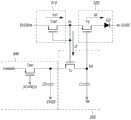
如图7所示,根据本公开内容的示例实施方式的子像素电路300可以包括参考电路310、发光电路320、放大电路330和输入电路340。As shown in FIG. 7 , the
参考电路310可以接收高电位电压EVDD并且可以控制流经发光电路320的驱动电流Id的变化。例如,当发光电路320的输入节点处的控制电压Vc与数据电压Vdata具有相同电位时,施加至放大电路330的电流I3变为0,使得流经参考电路310的参考电流Iref与流经发光电路320的驱动电流Id具有相同的值。The
在显示驱动时段期间,高电位电压EVDD可以具有显示图像所需的电平。例如,显示图像的高电位电压EVDD可以是27V,但是本公开内容不限于此。During the display driving period, the high potential voltage EVDD may have a level required to display an image. For example, the high potential voltage EVDD displaying an image may be 27V, but the present disclosure is not limited thereto.
发光电路320可以被定位在控制电压Vc与低电位电压EVSS之间,并且可以根据放大电路330的输出节点处的驱动电压Vd来控制发光元件ED的操作。当发光元件ED导通时,驱动电流Id可以流经发光电路320。The
低电位电压EVSS可以是地电压或者高于或低于地电压的电压。低电位电压EVSS可以根据驱动状态而变化。例如,显示驱动时的低电位电压EVSS与感测驱动时的低电位电压EVSS可以被设置为彼此不同。The low potential voltage EVSS may be a ground voltage or a voltage higher or lower than the ground voltage. The low potential voltage EVSS can vary according to the driving state. For example, the low potential voltage EVSS at the time of display driving and the low potential voltage EVSS at the time of sensing driving may be set to be different from each other.
放大电路330可以将控制电压Vc与数据电压Vdata进行比较,以生成用于控制发光电路320的操作的驱动电压Vd。例如,放大电路330可以由运算放大器形成,该运算放大器具有施加控制电压Vc的反相输入端子以及施加来自输入电路340的输出电压的非反相输入端子(+)。The
发光电路320的电阻值可以与放大电路330的驱动电压Vd成反比地减小。当控制电压Vc大于数据电压Vdata时,与放大电路330的输出节点对应的驱动电压Vd可以减小。The resistance value of the
因此,当控制电压Vc和数据电压Vdata具有相同电平时,放大电路330的操作可以停止,并且控制电压Vc可以保持与数据电压Vdata相同的电平。Accordingly, when the control voltage Vc and the data voltage Vdata have the same level, the operation of the amplifying
输入电路340可以通过扫描信号SCAN确定数据电压Vdata被施加至放大电路330的非反相输入端子(+)的时间。The
换言之,本公开内容的示例子像素电路300可以被控制为允许控制电压Vc保持与数据电压Vdata成比例的电平,使得流经发光元件ED的驱动电流Id与数据电压Vdata的电平成比例。因此,无论发光元件ED的劣化或驱动晶体管的特性值如何,与数据电压Vdata成比例的电流都可以流经发光元件ED,从而保持显示装置100的亮度持续。In other words, the
图8是示出根据本公开内容的示例实施方式的子像素电路的详细配置的图。FIG. 8 is a diagram illustrating a detailed configuration of a sub-pixel circuit according to an example embodiment of the present disclosure.
如图8所示,根据本公开内容的示例实施方式的子像素电路300可以包括参考电路310、发光电路320、放大电路330和输入电路340。下面描述例如构成显示面板110的多个子像素中的被施加第n个扫描信号SCAN(n)的示例子像素电路300。As shown in FIG. 8 , the
参考电路310可以包括参考晶体管Tref,参考晶体管Tref具有可以提供控制电压Vc的漏极节点和栅极节点,以及可以施加高电位电压EVDD的源极节点。The
发光电路320可以包括发光元件ED和驱动晶体管Td,发光元件ED具有可以施加低电位电压EVSS的阴极电极,驱动晶体管Td具有连接至发光元件的阳极电极的漏极节点、可以施加控制电压Vc的源极节点、以及可以施加放大电路330的驱动电压Vd的栅极节点。The
参考晶体管Tref可以在高电位电压EVDD被施加至源节点的同时导通,并且当驱动晶体管Td被放大电路330的驱动电压Vd导通时,驱动电流Id可以流经发光电路320。The reference transistor Tref may be turned on while the high potential voltage EVDD is applied to the source node, and when the driving transistor Td is turned on by the driving voltage Vd of the amplifying
在这种情况下,当控制电压Vc和数据电压Vdata具有相同电平的电位时,流经参考电路310的整个参考电流Iref可以流经发光电路320,并且驱动电流Id可以具有与参考电流Iref相同的值。In this case, when the control voltage Vc and the data voltage Vdata have the same level of potential, the entire reference current Iref flowing through the
放大电路330可以包括控制晶体管Tc、复位晶体管Trst和第一电容器Cl。控制晶体管Tc可以具有可以施加控制电压Vc的栅极节点以及连接至驱动晶体管Td的栅极节点的漏极节点。复位晶体管Trst可以具有接收复位电压Vrst的源极节点、可以施加第(n-1)个扫描信号SCAN(n-1)的栅极节点、以及与控制晶体管Tc共用的漏极节点。第一电容器C1可以连接至控制晶体管Tc的漏极节点以传递用于驱动驱动晶体管Td的电力电压Vp。The
可以以被配置成关断驱动晶体管Td的电压电平施加复位电压Vrst。The reset voltage Vrst may be applied at a voltage level configured to turn off the driving transistor Td.
可以在某个时间点处以能够驱动驱动晶体管Td的电平施加电力电压Vp,并且可以通过存储在第一电容器Cl中的电荷来改变该电平。换言之,电力电压Vp可能不会持续保持恒定的电压电平。The power voltage Vp can be applied at a level capable of driving the driving transistor Td at a certain point of time, and the level can be changed by the charge stored in the first capacitor C1. In other words, the power voltage Vp may not continuously maintain a constant voltage level.
输入电路340可以包括开关晶体管Tsw和第二电容器C2。开关晶体管Tsw可以具有可以施加第n个扫描信号SCAN(n)的栅极节点、可以施加数据电压Vdata的源极节点以及连接至控制晶体管Tc的源极节点的漏极节点。第二电容器C2可以连接在开关晶体管Tsw的漏极节点与低电位电压EVSS之间。The
因此,输入电路340可以通过第n个扫描信号SCAN(n)将数据电压Vdata供应给放大电路330。第二电容器C2可以用于稳定地传递数据电压Vdata。Accordingly, the
构成示例子像素电路300的晶体管Td、Tref、Tc、Trst和Tsw可以是P型晶体管或N型晶体管。The transistors Td, Tref, Tc, Trst, and Tsw constituting the
P型晶体管比N型晶体管相对更可靠。在P型晶体管的情况下,由于在发光元件ED发光的时段期间驱动晶体管Td可以被固定为高电位电压EVDD,所以可以无明显波动地稳定地供应流经发光元件ED的电流。P-type transistors are relatively more reliable than N-type transistors. In the case of a P-type transistor, since the drive transistor Td can be fixed at the high potential voltage EVDD during a period in which the light emitting element ED emits light, the current flowing through the light emitting element ED can be stably supplied without significant fluctuation.
当在饱和区中操作时,不管阈值电压的变化如何,P型晶体管可以流动恒定电流,从而提供相对高的可靠性。When operating in a saturation region, the P-type transistor can flow a constant current regardless of variations in threshold voltage, thereby providing relatively high reliability.
另一方面,由于N型晶体管使用电子而不是空穴作为载流子,因此N型晶体管比P型晶体管具有更高的迁移率,从而可以提高开关速度。On the other hand, since N-type transistors use electrons instead of holes as carriers, N-type transistors have higher mobility than P-type transistors, which can increase switching speed.
N型晶体管可以是由氧化物半导体形成的氧化物晶体管(例如,具有由诸如铟、镓、氧化锌或IGZO的氧化物半导体形成的沟道的晶体管)。P型晶体管可以是由诸如硅的半导体形成的硅晶体管(例如,具有通过称为LTPS的低温工艺形成的多晶硅沟道或低温多晶硅的晶体管)。The N-type transistor may be an oxide transistor formed of an oxide semiconductor (for example, a transistor having a channel formed of an oxide semiconductor such as indium, gallium, zinc oxide, or IGZO). The P-type transistor may be a silicon transistor formed from a semiconductor such as silicon (eg, a transistor having a polysilicon channel or low temperature polysilicon formed by a low temperature process called LTPS).
这里描述的是构成子像素电路300的晶体管Td、Tref、Tc、Trst和Tsw是P型晶体管的示例。Described here is an example in which the transistors Td, Tref, Tc, Trst, and Tsw constituting the
晶体管的术语“源极节点”和“漏极节点”可以根据输入电压互换使用。The terms "source node" and "drain node" of a transistor may be used interchangeably depending on the input voltage.
图9是示出根据本公开内容的示例实施方式的子像素电路的操作的示例信号波形图。FIG. 9 is an example signal waveform diagram illustrating an operation of a sub-pixel circuit according to an example embodiment of the present disclosure.
参照图9,下面描述由根据本公开内容的示例实施方式的显示装置100中的第n个扫描信号SCAN(n)驱动的子像素电路300的操作。Referring to FIG. 9 , the operation of the
如果复位晶体管Trst在第n个扫描信号SCAN(n)之前由第(n-1)个扫描信号SCAN(n-1)导通,则复位电压Vrst可以被施加至驱动晶体管Td的栅极节点以关断驱动晶体管Td。电力电压Vp可以增大到复位电压Vrst的电平。If the reset transistor Trst is turned on by the (n-1)th scan signal SCAN(n-1) before the n-th scan signal SCAN(n), the reset voltage Vrst may be applied to the gate node of the driving transistor Td to The driving transistor Td is turned off. The power voltage Vp may increase to the level of the reset voltage Vrst.
此后,如果施加第n个扫描信号SCAN(n)以导通开关晶体管Tsw,则可以将数据电压Vdata施加至第二电容器C2。在这种情况下,电力电压Vp可以以恒定斜率减小。如果电力电压Vp达到驱动晶体管Td的阈值电压电平,则驱动晶体管Td可以导通,并且流经参考电路310的参考电流Iref可以通过驱动晶体管Td传递至发光电路320。Thereafter, if the nth scan signal SCAN(n) is applied to turn on the switching transistor Tsw, the data voltage Vdata may be applied to the second capacitor C2. In this case, the power voltage Vp may decrease with a constant slope. If the power voltage Vp reaches the threshold voltage level of the driving transistor Td, the driving transistor Td may be turned on, and the reference current Iref flowing through the
与参考电路310的输出电压对应的控制电压Vc可以通过参考电流Iref以及从参考电路310流经发光电路320的驱动电流Id降低。The control voltage Vc corresponding to the output voltage of the
如果控制电压Vc降低并达到数据电压Vdata和控制晶体管Tc的阈值电压Vth(Tc)之和Vdata+Vth(Tc),则控制晶体管Tc可以导通。如果控制晶体管Tc导通,则存储在第一电容器C1中的电荷可以移动到第二电容器C2,使得流经驱动晶体管Td的驱动电流Id可以减小。因此,控制电压Vc可以增大,并且控制晶体管Tc可以被关断。If the control voltage Vc decreases and reaches the sum Vdata+Vth(Tc) of the data voltage Vdata and the threshold voltage Vth(Tc) of the control transistor Tc, the control transistor Tc may be turned on. If the control transistor Tc is turned on, the charge stored in the first capacitor C1 may be moved to the second capacitor C2 so that the driving current Id flowing through the driving transistor Td may be reduced. Therefore, the control voltage Vc can be increased, and the control transistor Tc can be turned off.
随着控制晶体管Tc在短时段内重复导通和关断,控制电压Vc可以保持数据电压Vdata和控制晶体管Tc的阈值电压Vth(Tc)之和Vdata+Vth(Tc)的电平。As the control transistor Tc is repeatedly turned on and off for a short period of time, the control voltage Vc may maintain a level of the sum of the data voltage Vdata and the threshold voltage Vth(Tc) of the control transistor Tc Vdata+Vth(Tc).
在这种状态下,流经参考晶体管Tref的参考电流Iref在饱和区可以被表示如下:In this state, the reference current Iref flowing through the reference transistor Tref in the saturation region can be expressed as follows:
Iref=K*[(Vc-Vth(Tref)]2=K*[(Vdata+Vth(Tc)-Vth(Tref)]2Iref=K*[(Vc-Vth(Tref)]2 =K*[(Vdata+Vth(Tc)-Vth(Tref)]2
这里,K=Cox*(W/L)*μ,W和L分别表示参考晶体管Tref的沟道宽度和长度,Cox表示栅极绝缘膜的电容,μ表示参考晶体管Tref的迁移率。Here, K=Cox*(W/L)*μ, W and L denote the channel width and length of the reference transistor Tref, respectively, Cox denotes the capacitance of the gate insulating film, and μ denotes the mobility of the reference transistor Tref.
在这种情况下,如果彼此相邻定位的控制晶体管Tc和参考晶体管Tref的沉积条件保持相同,则控制晶体管Tc的阈值电压Vth(Tc)和参考晶体管Tref的阈值电压Vth(Tref)可以具有相同的值。换言之,控制晶体管Tc和参考晶体管Tref可以通过在沉积控制晶体管Tc和参考晶体管Tref的过程中在相同条件下保持栅极节点、源极节点、漏极节点以及位于它们之间的绝缘膜的厚度和组成比而被形成为具有相同的阈值电压Vth。In this case, if the deposition conditions of the control transistor Tc and the reference transistor Tref positioned adjacent to each other remain the same, the threshold voltage Vth(Tc) of the control transistor Tc and the threshold voltage Vth(Tref) of the reference transistor Tref can have the same value. In other words, the control transistor Tc and the reference transistor Tref can be obtained by maintaining the thicknesses and The composition ratios are formed to have the same threshold voltage Vth.
如果控制晶体管Tc的阈值电压Vth(Tc)和参考晶体管Tref的阈值电压Vth(Tref)具有相同的值,则流经参考晶体管Tref的参考电流Iref可以被表示为:If the threshold voltage Vth(Tc) of the control transistor Tc and the threshold voltage Vth(Tref) of the reference transistor Tref have the same value, the reference current Iref flowing through the reference transistor Tref can be expressed as:
Iref=K*Vdata2Iref=K*Vdata2
换言之,由于流经发光元件ED的驱动电流Id和流经参考晶体管Tref的参考电流Iref均与数据电压Vdata成比例,因此无论发光元件ED的特性或驱动晶体管Td的特性值如何,用于驱动发光元件ED的驱动电流Id都可以通过数据电压Vdata来调整。In other words, since both the driving current Id flowing through the light emitting element ED and the reference current Iref flowing through the reference transistor Tref are proportional to the data voltage Vdata, regardless of the characteristic value of the light emitting element ED or the characteristic value of the driving transistor Td, it is used to drive light emission. The driving current Id of the element ED can be adjusted by the data voltage Vdata.
另一方面,如果驱动晶体管Td是氧化物晶体管,则阈值电压Vth会因正偏压温度应力(PBTS)而偏移。但是在这种情况下,可以通过增大高电位电压EVDD的幅度以增大流经发光元件ED的驱动电流Id并降低驱动晶体管Td的栅极-源极节点电压来使阈值电压Vth的变化最小化。On the other hand, if the driving transistor Td is an oxide transistor, the threshold voltage Vth is shifted due to positive bias temperature stress (PBTS). In this case, however, the change in the threshold voltage Vth can be minimized by increasing the magnitude of the high potential voltage EVDD to increase the drive current Id flowing through the light emitting element ED and lowering the gate-source node voltage of the drive transistor Td change.
例如,可以将高电位电压EVDD设置为28V或更高以减少由于正偏压温度应力(PBTS)引起的驱动晶体管Td的阈值电压Vth的偏移。For example, the high-potential voltage EVDD may be set to 28 V or higher to reduce a shift in the threshold voltage Vth of the driving transistor Td due to positive bias temperature stress (PBTS).
因此,本公开内容的示例子像素电路300可以通过允许与参考电路310的输出电压对应的控制电压Vc保持与控制晶体管Tc的阈值电压Vth(Tc)和数据电压Vdata之和Vdata+Vth(Tc)对应的电平来进行控制,以允许流经发光元件ED的驱动电流Id与数据电压Vdata的电平成比例。因此,在本公开内容的示例子像素电路300中,无论发光元件ED的劣化或驱动晶体管Td的特性值如何,与数据电压Vdata成比例的电流都可以流经发光元件ED。因此,可以提供具有均匀亮度的显示面板110和显示装置100。Therefore, the
图10是示出根据本公开内容的示例实施方式的流经参考电路的电流根据子像素电路中的数据电压而变化的信号波形图。FIG. 10 is a signal waveform diagram illustrating a change in a current flowing through a reference circuit according to a data voltage in a sub-pixel circuit according to an example embodiment of the present disclosure. Referring to FIG.
如图10所示,可以控制根据本公开内容的示例实施方式的子像素电路300,通过允许参考电路310的输出节点的控制电压Vc保持在与控制晶体管Tc的阈值电压Vth(Tc)和数据电压Vdata之和Vdata+Vth(Tc)对应的电平,使得流经发光电路320的驱动电流Id和流经参考电路310的参考电流Iref与数据电压Vdata的电平成比例。As shown in FIG. 10 , the
例如,当控制电压Vc保持在与控制晶体管Tc的阈值电压Vth(Tc)和数据电压Vdata之和Vdata+Vth(Tc)对应的电平时,流经发光电路320的驱动电流Id和流经参考电路310的参考电流Iref可以保持相同的值。在这种情况下,可以识别出,当数据电压Vdata依次变为22V、21V、20V、19V和18V的电平时,流经发光电路320的驱动电流Id和流经参考电路310的参考电流Iref均具有基本上与数据电压Vdata成比例的值。For example, when the control voltage Vc is maintained at a level corresponding to the sum Vdata+Vth(Tc) of the threshold voltage Vth(Tc) of the control transistor Tc and the data voltage Vdata, the driving current Id flowing through the
图11A、图11B和图11C是示出根据本公开内容的示例实施方式的当驱动晶体管在子像素电路中具有不同阈值电压时子像素电路的电流和电压变化的信号波形图。11A , 11B and 11C are signal waveform diagrams illustrating current and voltage changes of sub-pixel circuits when driving transistors have different threshold voltages in the sub-pixel circuits according to example embodiments of the present disclosure.
如图11A、图11B和图11C所示,在根据本公开内容的示例实施方式的子像素电路300中,诸如驱动晶体管Td的阈值电压的特性值可以随着驱动时间增加而改变。As shown in FIGS. 11A , 11B, and 11C, in the
考虑到这种情况,在驱动晶体管Td的阈值电压具有参考电压并且从参考电压增大1V的情况下,测量与放大电路330的输出电压对应的驱动电压Vd、与参考电路310的输出电压对应的控制电压Vc以及流经发光电路320的驱动电流Id的变化。In consideration of this, in the case where the threshold voltage of the driving transistor Td has the reference voltage and is increased by 1 V from the reference voltage, the driving voltage Vd corresponding to the output voltage of the
可以确定,当驱动晶体管Td的阈值电压增大时,与放大电路330的输出电压对应的驱动电压Vd的电平发生变化(图11A的情况)。It was confirmed that when the threshold voltage of the driving transistor Td increases, the level of the driving voltage Vd corresponding to the output voltage of the amplifying
然而,尽管驱动晶体管Td的阈值电压增大,但是与参考电路310的输出电压对应的控制电压Vc始终保持在与控制晶体管Tc的阈值电压Vth(Tc)和数据电压Vdata之和Vdata+Vth(Tc)对应的电平(图11B的情况)。However, although the threshold voltage of the driving transistor Td increases, the control voltage Vc corresponding to the output voltage of the
因此,尽管驱动晶体管Td的阈值电压改变了,但是流经发光电路320的驱动电流Id和流经参考电路310的参考电流Iref可以保持恒定值(图11C的情况)。Therefore, although the threshold voltage of the driving transistor Td changes, the driving current Id flowing through the
这样,由于无论本公开内容的发光元件ED的劣化或子像素电路300中的驱动晶体管Td的特性值如何,流经发光元件ED的驱动电流Id都具有与数据电压Vdata成比例的值,因此尽管驱动时间增加,但是显示装置100可以保持均匀的亮度。In this way, since the driving current Id flowing through the light emitting element ED has a value proportional to the data voltage Vdata regardless of the deterioration of the light emitting element ED of the present disclosure or the characteristic value of the driving transistor Td in the
在本公开内容的示例子像素电路300中,放大电路330可以替选地通过控制电力电压Vp而不是实现复位晶体管Trst来使驱动晶体管Td复位。In the
图12是示出根据本公开内容的示例实施方式的另一子像素电路的详细配置的图。FIG. 12 is a diagram illustrating a detailed configuration of another sub-pixel circuit according to an example embodiment of the present disclosure.
如图12所示,根据本公开内容的示例实施方式的子像素电路300可以包括参考电路310、发光电路320、放大电路330和输入电路340。下面描述其中在构成显示面板110的多个子像素之间施加第n个扫描信号SCAN(n)的示例。As shown in FIG. 12 , the
参考电路310可以包括参考晶体管Tref,参考晶体管Tref具有可以提供控制电压Vc的漏极节点和栅极节点以及可以施加高电位电压EVDD的源极节点。The
发光电路320可以包括发光元件ED和驱动晶体管Td,发光元件ED具有可以施加低电位电压EVSS的阴极电极,驱动晶体管Td具有连接至发光元件ED的阳极电极的漏极节点、可以施加控制电压Vc的源极节点、以及可以施加放大电路330的驱动电压Vd的栅极节点。The
参考晶体管Tref可以由高电位电压EVDD导通,并且当驱动晶体管Td由放大电路330的驱动电压Vd导通时,驱动电流Id可以流经发光电路320。The reference transistor Tref may be turned on by the high potential voltage EVDD, and when the driving transistor Td is turned on by the driving voltage Vd of the amplifying
在这种情况下,当控制电压Vc和数据电压Vdata具有相同电平的电位时,流经参考电路310的整个参考电流Iref可以流经发光电路320,并且驱动电流Id可以具有与参考电流Iref相同的值。In this case, when the control voltage Vc and the data voltage Vdata have the same level of potential, the entire reference current Iref flowing through the
放大电路330可以包括控制晶体管Tc和第一电容器Cl。控制晶体管Tc可以具有可以施加控制电压Vc的栅极节点以及连接至驱动晶体管Td的栅极节点的漏极节点。第一电容器C1可以连接至控制晶体管Tc的漏极节点以传递用于驱动驱动晶体管Td的电力电压Vp。电力电压Vp可以具有能够驱动驱动晶体管Td的电平。The
输入电路340可以包括开关晶体管Tsw和第二电容器C2。开关晶体管Tsw可以具有可以施加第n个扫描信号SCAN(n)的栅极节点、可以施加数据电压Vdata的源极节点以及连接至控制晶体管Tc的源极节点的漏极节点。第二电容器C2可以连接在开关晶体管Tsw的漏极节点与低电位电压EVSS之间。The
因此,输入电路340可以通过第n个扫描信号SCAN(n)将数据电压Vdata供应给放大电路330。第二电容器C2可以用于稳定地传递数据电压Vdata。Accordingly, the
构成示例子像素电路300的晶体管Td、Tref、Tc和Tsw可以是P型晶体管或N型晶体管。The transistors Td, Tref, Tc, and Tsw constituting the
P型晶体管比N型晶体管相对更可靠。在P型晶体管的情况下,由于在发光元件ED发光的时段期间驱动晶体管Td可以被固定为高电位电压EVDD,所以可以无明显波动地稳定地供应流经发光元件ED的电流。P-type transistors are relatively more reliable than N-type transistors. In the case of a P-type transistor, since the drive transistor Td can be fixed at the high potential voltage EVDD during a period in which the light emitting element ED emits light, the current flowing through the light emitting element ED can be stably supplied without significant fluctuation.
当在饱和区中操作时,无论阈值电压的变化如何,P型晶体管都可以流过恒定电流,从而提供相对高的可靠性。When operating in a saturation region, the P-type transistor can flow a constant current regardless of changes in threshold voltage, thereby providing relatively high reliability.
另一方面,由于N型晶体管使用电子而不是空穴作为载流子,因此N型晶体管具有比P型晶体管更高的迁移率,从而可以提高开关速度。On the other hand, since N-type transistors use electrons instead of holes as carriers, N-type transistors have higher mobility than P-type transistors, which can increase switching speed.
N型晶体管可以是由氧化物半导体形成的氧化物晶体管(例如,具有由诸如铟、镓、氧化锌或IGZO的氧化物半导体形成的沟道的晶体管)。P型晶体管可以是由诸如硅的半导体形成的硅晶体管(例如,具有通过称为LTPS的低温工艺形成的多晶硅沟道或低温多晶硅的晶体管)。The N-type transistor may be an oxide transistor formed of an oxide semiconductor (for example, a transistor having a channel formed of an oxide semiconductor such as indium, gallium, zinc oxide, or IGZO). The P-type transistor may be a silicon transistor formed from a semiconductor such as silicon (eg, a transistor having a polysilicon channel or low temperature polysilicon formed by a low temperature process called LTPS).
这里描述的是构成子像素电路300的晶体管Td、Tref、Tc和Tsw是P型晶体管的示例。Described here is an example in which the transistors Td, Tref, Tc, and Tsw constituting the
晶体管的术语“源极节点”和“漏极节点”可以根据输入电压互换使用。The terms "source node" and "drain node" of a transistor may be used interchangeably depending on the input voltage.
图13是示出根据本公开内容的示例实施方式的另一子像素电路的操作的示例信号波形图。FIG. 13 is an example signal waveform diagram illustrating an operation of another sub-pixel circuit according to an example embodiment of the present disclosure.
下面参照图13描述根据本公开内容的示例实施方式的子像素电路300的操作。The operation of the
可以根据一个或更多个时序信号从电力管理电路150以脉冲的形式施加电力电压Vp。The power voltage Vp may be applied in pulses from the
如果在施加第n个扫描信号SCAN(n)之前以高电平施加电力电压Vp,则驱动晶体管Td可以由电力电压Vp关断。If the power voltage Vp is applied at a high level before the n-th scan signal SCAN(n) is applied, the driving transistor Td may be turned off by the power voltage Vp.
此后,如果施加第n个扫描信号SCAN(n)以使开关晶体管Tsw导通,则可以将数据电压Vdata施加至第二电容器C2。在施加第n个扫描信号SCAN(n)之后,电力电压Vp可以被切换到低电平。如果电力电压Vp达到驱动晶体管Td的阈值电压电平,则驱动晶体管Td可以导通,并且流经参考电路310的参考电流Iref可以通过驱动晶体管Td传递至发光电路320。Thereafter, if the nth scan signal SCAN(n) is applied to turn on the switching transistor Tsw, the data voltage Vdata may be applied to the second capacitor C2. After the n-th scan signal SCAN(n) is applied, the power voltage Vp may be switched to a low level. If the power voltage Vp reaches the threshold voltage level of the driving transistor Td, the driving transistor Td may be turned on, and the reference current Iref flowing through the
与参考电路310的输出电压对应的控制电压Vc可以由参考电流Iref和从参考电路310流经发光电路320的驱动电流Id降低。The control voltage Vc corresponding to the output voltage of the
如果控制电压Vc达到数据电压Vdata和控制晶体管Tc的阈值电压Vth(Tc)之和Vdata+Vth(Tc)的电平,则控制晶体管Tc可以导通。如果控制晶体管Tc导通,则存储在第一电容器C1中的电荷会移动到第二电容器C2,使得流经驱动晶体管Td的驱动电流Id会减小。因此,控制电压Vc可以增大,并且控制晶体管Tc可以被关断。If the control voltage Vc reaches the level of the sum of the data voltage Vdata and the threshold voltage Vth(Tc) of the control transistor Tc, Vdata+Vth(Tc), the control transistor Tc may be turned on. If the control transistor Tc is turned on, the charges stored in the first capacitor C1 are moved to the second capacitor C2, so that the driving current Id flowing through the driving transistor Td is reduced. Therefore, the control voltage Vc can be increased, and the control transistor Tc can be turned off.
随着控制晶体管Tc在短时段内重复导通和关断,控制电压Vc可以保持数据电压Vdata和控制晶体管Tc的阈值电压Vth(Tc)之和Vdata+Vth(Tc)的电平。As the control transistor Tc is repeatedly turned on and off for a short period of time, the control voltage Vc may maintain a level of the sum of the data voltage Vdata and the threshold voltage Vth(Tc) of the control transistor Tc Vdata+Vth(Tc).
在这种情况下,如果彼此相邻定位的控制晶体管Tc和参考晶体管Tref的沉积条件相同,则控制晶体管Tc的阈值电压Vth(Tc)和参考晶体管Tref的阈值电压Vth(Tref)可以具有相同的值。换言之,控制晶体管Tc和参考晶体管Tref可以通过在沉积控制晶体管Tc和参考晶体管Tref的过程中在相同条件下保持栅极节点、源极节点、漏极节点以及位于它们之间的绝缘膜的厚度和组成比而被形成为具有相同的阈值电压Vth。In this case, if the deposition conditions of the control transistor Tc and the reference transistor Tref located adjacent to each other are the same, the threshold voltage Vth(Tc) of the control transistor Tc and the threshold voltage Vth(Tref) of the reference transistor Tref can have the same value. In other words, the control transistor Tc and the reference transistor Tref can be obtained by maintaining the thicknesses and The composition ratios are formed to have the same threshold voltage Vth.
如果控制晶体管Tc的阈值电压Vth(Tc)和参考晶体管Tref的阈值电压Vth(Tref)具有相同的值,则流经参考晶体管Tref的参考电流Iref可以被表示为:If the threshold voltage Vth(Tc) of the control transistor Tc and the threshold voltage Vth(Tref) of the reference transistor Tref have the same value, the reference current Iref flowing through the reference transistor Tref can be expressed as:
Iref=K*Vdata2Iref=K*Vdata2
换言之,由于流经发光元件ED的驱动电流Id和流经参考晶体管Tref的参考电流Iref均与数据电压Vdata成比例,因此无论发光元件ED的特性或驱动晶体管Td的特性值如何,用于驱动发光元件ED的驱动电流Id都可以通过数据电压Vdata来调整。In other words, since both the driving current Id flowing through the light emitting element ED and the reference current Iref flowing through the reference transistor Tref are proportional to the data voltage Vdata, regardless of the characteristic value of the light emitting element ED or the characteristic value of the driving transistor Td, it is used to drive light emission. The driving current Id of the element ED can be adjusted by the data voltage Vdata.
因此,本公开内容的示例子像素电路300可以通过允许与参考电路310的输出电压对应的控制电压Vc保持在与控制晶体管Tc的阈值电压Vth(Tc)和数据电压Vdata之和Vdata+Vth(Tc)对应的电平来进行控制,以允许流经发光元件ED的驱动电流Id与数据电压Vdata的电平成比例。Therefore, the
因此,在本公开内容的示例子像素电路300中,无论发光元件ED的劣化或驱动晶体管Td的特性值如何,与数据电压Vdata成比例的电流都可以流经发光元件ED。因此,可以提供具有均匀亮度的显示面板110和显示装置100。Therefore, in the
下面简要描述前述示例实施方式。The aforementioned example embodiments are briefly described below.
一种用于操作设置在显示面板上的多个子像素中的至少一个子像素的子像素电路可以包括:参考电路,其被配置成接收高电位电压并且输出用于控制流经发光元件的驱动电流的控制电压;发光电路,其包括发光元件,发光电路被配置成接收控制电压和低电位电压,并且基于驱动电压控制发光元件;放大电路,其被配置成将控制电压与数据电压进行比较以生成用于控制发光电路的驱动电压;以及输入电路,其被配置成接收数据电压和第一扫描信号,并且基于第一扫描信号来控制将数据电压施加至放大电路的时序。A subpixel circuit for operating at least one subpixel among a plurality of subpixels disposed on a display panel may include: a reference circuit configured to receive a high potential voltage and output a driving current for controlling a flow of a light emitting element a control voltage; a light emitting circuit including a light emitting element configured to receive a control voltage and a low potential voltage, and to control the light emitting element based on the driving voltage; an amplifying circuit configured to compare the control voltage with a data voltage to generate a driving voltage for controlling the light emitting circuit; and an input circuit configured to receive the data voltage and the first scan signal, and control timing of applying the data voltage to the amplification circuit based on the first scan signal.
在一些实施方式中,参考电路可以包括参考晶体管,该参考晶体管具有提供控制电压的漏极节点和栅极节点以及接收高电位电压的源极节点。In some implementations, the reference circuit may include a reference transistor having a drain node and a gate node supplying a control voltage and a source node receiving a high potential voltage.
在一些实施方式中,发光电路可以包括:发光元件,其具有接收低电位电压的阴极电极;以及驱动晶体管,其具有连接至发光元件的阳极电极的漏极节点以及接收驱动电压的栅极节点。In some embodiments, the light emitting circuit may include: a light emitting element having a cathode electrode receiving a low potential voltage; and a driving transistor having a drain node connected to the anode electrode of the light emitting element and a gate node receiving a driving voltage.
在一些实施方式中,放大电路可以包括运算放大器,运算放大器具有接收控制电压的反相输入端子、接收输入电路的输出电压的非反相输入端子和输出驱动电压的输出端子。In some embodiments, the amplifying circuit may include an operational amplifier having an inverting input terminal receiving a control voltage, a non-inverting input terminal receiving an output voltage of the input circuit, and an output terminal outputting a driving voltage.
在一些实施方式中,放大电路可以包括:控制晶体管,其具有接收控制电压的栅极节点以及向发光电路提供驱动电压的漏极节点;以及第一电容器,其连接至控制晶体管的漏极节点以传递输入电力电压。In some embodiments, the amplifying circuit may include: a control transistor having a gate node receiving a control voltage and a drain node supplying a driving voltage to the light emitting circuit; and a first capacitor connected to the drain node of the control transistor to Passes the input power voltage.
在一些实施方式中,参考电路可以包括参考晶体管,参考晶体管具有被配置成提供控制电压的漏极节点和栅极节点以及被配置成接收高电位电压的源极节点;并且控制晶体管和参考晶体管可以具有相同的阈值电压。In some embodiments, the reference circuit may include a reference transistor having a drain node and a gate node configured to provide a control voltage and a source node configured to receive a high potential voltage; and the control transistor and the reference transistor may have the same threshold voltage.
在一些实施方式中,控制晶体管和参考晶体管可以具有以下项中的至少一项:栅极节点、源极节点、漏极节点和位于栅极节点与源极节点和漏极节点之间的绝缘膜的相同的厚度、相同的组成比以及相同的结构。In some embodiments, the control transistor and the reference transistor may have at least one of: a gate node, a source node, a drain node, and an insulating film between the gate node and the source node and the drain node The same thickness, the same composition ratio and the same structure.
在一些实施方式中,放大电路还可以包括复位晶体管,该复位晶体管具有接收复位电压的源极节点、在输入电路接收第一扫描信号之前接收第二扫描信号的栅极节点、以及与控制晶体管共用的漏极节点。In some embodiments, the amplifying circuit may further include a reset transistor, which has a source node receiving a reset voltage, a gate node receiving a second scan signal before the input circuit receives the first scan signal, and a gate node shared with the control transistor. the drain node.
在一些实施方式中,驱动晶体管可以被配置成由第二扫描信号复位以及由第一扫描信号导通。In some embodiments, the driving transistor may be configured to be reset by the second scan signal and turned on by the first scan signal.
在一些实施方式中,在与数据电压和控制晶体管的阈值电压之和对应的电平的控制电压下,流经发光电路的驱动电流与流经参考电路的参考电流可以具有相同的值。In some embodiments, the driving current flowing through the light emitting circuit and the reference current flowing through the reference circuit may have the same value under the control voltage at a level corresponding to the sum of the data voltage and the threshold voltage of the control transistor.
在一些实施方式中,输入电路可以包括:开关晶体管,其具有接收第一扫描信号的栅极节点、接收数据电压的源极节点以及连接至放大电路的漏极节点;以及第二电容器,其连接在开关晶体管的漏极与低电位电压之间。In some embodiments, the input circuit may include: a switching transistor having a gate node receiving the first scan signal, a source node receiving the data voltage, and a drain node connected to the amplifying circuit; and a second capacitor connected to Between the drain of the switching transistor and the low potential voltage.
在一些实施方式中,发光电路可以包括驱动晶体管,驱动晶体管具有连接至发光元件的阳极电极的漏极节点以及接收驱动电压的栅极节点;驱动晶体管可以被配置成在输入电路接收到第一扫描信号之前由输入电力电压复位以及由第一扫描信号导通。In some embodiments, the light emitting circuit may include a driving transistor having a drain node connected to the anode electrode of the light emitting element and a gate node receiving a driving voltage; the driving transistor may be configured to receive the first scanning voltage when the input circuit The signal was previously reset by the input power voltage and turned on by the first scan signal.
在一些实施方式中,发光电路、参考电路、放大电路和输入电路可以包括P型晶体管。In some embodiments, the light emitting circuit, the reference circuit, the amplifier circuit and the input circuit may include P-type transistors.
在一些实施方式中,驱动电流可以与数据电压成比例。In some implementations, the driving current may be proportional to the data voltage.
在一些实施方式中,显示面板可以包括多个子像素和任何上述实施方式的子像素电路。In some embodiments, a display panel may include a plurality of sub-pixels and any of the sub-pixel circuits of the above-described embodiments.
一种显示装置可以包括:显示面板,其包括多个子像素和用于操作多个子像素中的至少一个子像素的子像素电路;栅极驱动电路,其被配置成通过多个栅极线分别向显示面板供应多个扫描信号;数据驱动电路,其被配置成通过多个数据线分别向显示面板供应多个数据电压;以及时序控制器,其被配置成驱动栅极驱动电路和数据驱动电路。在此,子像素电路可以包括:参考电路,其被配置成接收高电位电压并且输出用于控制流经发光元件的驱动电流的控制电压;发光电路,其包括发光元件,发光电路被配置成接收控制电压和低电位电压,并且基于驱动电压控制发光元件;放大电路,其被配置成将控制电压与数据电压进行比较以生成用于控制发光电路的驱动电压;以及输入电路,其被配置成接收数据电压和第一扫描信号,并且基于第一扫描信号来控制将数据电压施加至放大电路的时序。A display device may include: a display panel including a plurality of sub-pixels and a sub-pixel circuit for operating at least one of the plurality of sub-pixels; The display panel supplies a plurality of scan signals; a data driving circuit configured to respectively supply a plurality of data voltages to the display panel through a plurality of data lines; and a timing controller configured to drive the gate driving circuit and the data driving circuit. Here, the sub-pixel circuit may include: a reference circuit configured to receive a high potential voltage and output a control voltage for controlling a driving current flowing through the light emitting element; a light emitting circuit including a light emitting element configured to receive a control voltage and a low-potential voltage, and control a light emitting element based on the driving voltage; an amplification circuit configured to compare the control voltage with a data voltage to generate a driving voltage for controlling the light emitting circuit; and an input circuit configured to receive The data voltage and the first scan signal, and the timing of applying the data voltage to the amplifying circuit is controlled based on the first scan signal.
在一些实施方式中,放大电路可以包括:控制晶体管,其具有接收控制电压的栅极节点以及向发光电路提供驱动电压的漏极节点;以及第一电容器,其连接至控制晶体管的漏极节点以传递输入电力电压。In some embodiments, the amplifying circuit may include: a control transistor having a gate node receiving a control voltage and a drain node supplying a driving voltage to the light emitting circuit; and a first capacitor connected to the drain node of the control transistor to Passes the input power voltage.
在一些实施方式中,参考电路可以包括参考晶体管,该参考晶体管具有被配置成提供控制电压的漏极节点和栅极节点以及被配置成接收高电位电压的源极节点;控制晶体管和参考晶体管可以具有相同的阈值电压。In some implementations, the reference circuit may include a reference transistor having a drain node and a gate node configured to provide a control voltage and a source node configured to receive a high potential voltage; the control transistor and the reference transistor may have the same threshold voltage.
在一些实施方式中,放大电路还可以包括复位晶体管,该复位晶体管具有接收复位电压的源极节点、在输入电路接收到第一扫描信号之前接收第二扫描信号的栅极节点、以及与控制晶体管共用的漏极节点;并且驱动晶体管可以被配置成由第二扫描信号复位以及由第一扫描信号导通。In some embodiments, the amplifying circuit may further include a reset transistor having a source node receiving a reset voltage, a gate node receiving a second scan signal before the input circuit receives the first scan signal, and a control transistor a common drain node; and the driving transistor may be configured to be reset by the second scan signal and turned on by the first scan signal.
在一些实施方式中,驱动电流与数据电压成比例。In some embodiments, the drive current is proportional to the data voltage.
已经呈现以上描述以使本领域的任何技术人员能够制作和使用本公开内容的各种可能的实施方式。尽管已经参照附图更详细地描述了本公开内容的实施方式,但是本公开内容不限于此,并且在不脱离本公开内容的技术构思的情况下,可以以许多不同的形式体现。因此,本公开内容中公开的示例实施方式仅出于说明性目的而提供,并且不旨在限制本公开内容的技术构思。因此,应当理解,上述示例性实施方式在所有方面都是说明性的,并且不限制本公开内容。The above description has been presented to enable any person skilled in the art to make and use the various possible implementations of the present disclosure. Although the embodiments of the present disclosure have been described in more detail with reference to the accompanying drawings, the present disclosure is not limited thereto and can be embodied in many different forms without departing from the technical concept of the present disclosure. Therefore, the exemplary embodiments disclosed in the present disclosure are provided for illustrative purposes only, and are not intended to limit the technical idea of the present disclosure. Therefore, it should be understood that the above-described exemplary embodiments are illustrative in all respects and not restrictive of the present disclosure.
对于本领域技术人员而言将明显的是,在不脱离本公开内容的精神或范围的情况下,可以在本公开内容中做出各种修改和变型。因此,本公开内容旨在覆盖本公开内容的修改和变化,只要它们落入所附权利要求及其等同物的范围内。It will be apparent to those skilled in the art that various modifications and variations can be made in the present disclosure without departing from the spirit or scope of the disclosure. Thus, it is intended that the present disclosure cover the modifications and variations of this disclosure provided they come within the scope of the appended claims and their equivalents.
Claims (20)
Translated fromChineseApplications Claiming Priority (2)
| Application Number | Priority Date | Filing Date | Title |
|---|---|---|---|
| KR10-2021-0182406 | 2021-12-20 | ||
| KR1020210182406AKR20230093619A (en) | 2021-12-20 | 2021-12-20 | Subpixel circuit, display panwel and display device |
Publications (2)
| Publication Number | Publication Date |
|---|---|
| CN116364010Atrue CN116364010A (en) | 2023-06-30 |
| CN116364010B CN116364010B (en) | 2025-10-14 |
Family
ID=
Citations (5)
| Publication number | Priority date | Publication date | Assignee | Title |
|---|---|---|---|---|
| US20040144978A2 (en)* | 2001-02-26 | 2004-07-29 | Semiconductor Energy Laboratory Co., Ltd. | Organic light emitting device with constant luminance |
| CN108447443A (en)* | 2018-05-14 | 2018-08-24 | 京东方科技集团股份有限公司 | Pixel circuit, driving method, and display device |
| CN109637440A (en)* | 2019-01-15 | 2019-04-16 | 友达光电股份有限公司 | Pixel-driving circuit and its operating method |
| KR20200036588A (en)* | 2018-09-28 | 2020-04-07 | 엘지디스플레이 주식회사 | Organic Light Emitting Display having a Compensation Circuit for Driving Characteristic |
| CN112967681A (en)* | 2021-04-06 | 2021-06-15 | 上海天马微电子有限公司 | Drive circuit, light-emitting component and display device |
Patent Citations (5)
| Publication number | Priority date | Publication date | Assignee | Title |
|---|---|---|---|---|
| US20040144978A2 (en)* | 2001-02-26 | 2004-07-29 | Semiconductor Energy Laboratory Co., Ltd. | Organic light emitting device with constant luminance |
| CN108447443A (en)* | 2018-05-14 | 2018-08-24 | 京东方科技集团股份有限公司 | Pixel circuit, driving method, and display device |
| KR20200036588A (en)* | 2018-09-28 | 2020-04-07 | 엘지디스플레이 주식회사 | Organic Light Emitting Display having a Compensation Circuit for Driving Characteristic |
| CN109637440A (en)* | 2019-01-15 | 2019-04-16 | 友达光电股份有限公司 | Pixel-driving circuit and its operating method |
| CN112967681A (en)* | 2021-04-06 | 2021-06-15 | 上海天马微电子有限公司 | Drive circuit, light-emitting component and display device |
Also Published As
| Publication number | Publication date |
|---|---|
| US20230197001A1 (en) | 2023-06-22 |
| EP4198957B1 (en) | 2024-10-09 |
| KR20230093619A (en) | 2023-06-27 |
| EP4198957A1 (en) | 2023-06-21 |
| US11862089B2 (en) | 2024-01-02 |
Similar Documents
| Publication | Publication Date | Title |
|---|---|---|
| CN111199698B (en) | Method of sensing characteristic value of circuit element and display device using same | |
| CN116092440B (en) | Display device and driving circuit | |
| CN115831070B (en) | Display device and display driving method | |
| CN116110335B (en) | Display device, display panel, and display driving method | |
| US11783784B2 (en) | Display device, driving circuit and driving method | |
| US11527210B2 (en) | Method of sensing characteristic value of circuit element and display device using it | |
| US11935475B2 (en) | Display device, driving circuit and display driving method | |
| US11783755B2 (en) | Display device and display driving method | |
| US11869436B2 (en) | Subpixel circuit, display panel, and display device | |
| KR102665519B1 (en) | Display Device and Compensation Method | |
| CN116364010B (en) | Sub-pixel circuit, display panel, and display device | |
| US11862089B2 (en) | Subpixel circuit, display panel, and display device | |
| US20250148982A1 (en) | Display device, driving circuit, and display driving method | |
| US20250087157A1 (en) | Subpixel circuit, display panel and display device | |
| US20250259591A1 (en) | Pixel Circuit and Display Device Including the Same | |
| KR102687609B1 (en) | Display Device and Compensation Method |
Legal Events
| Date | Code | Title | Description |
|---|---|---|---|
| PB01 | Publication | ||
| PB01 | Publication | ||
| SE01 | Entry into force of request for substantive examination | ||
| SE01 | Entry into force of request for substantive examination | ||
| GR01 | Patent grant |