CN116344552A - Oxide semiconductor thin film transistor device and method of manufacturing the same - Google Patents
Oxide semiconductor thin film transistor device and method of manufacturing the sameDownload PDFInfo
- Publication number
- CN116344552A CN116344552ACN202310284050.6ACN202310284050ACN116344552ACN 116344552 ACN116344552 ACN 116344552ACN 202310284050 ACN202310284050 ACN 202310284050ACN 116344552 ACN116344552 ACN 116344552A
- Authority
- CN
- China
- Prior art keywords
- oxide semiconductor
- gate electrode
- layer
- source
- thin film
- Prior art date
- Legal status (The legal status is an assumption and is not a legal conclusion. Google has not performed a legal analysis and makes no representation as to the accuracy of the status listed.)
- Pending
Links
Images


Classifications
- H—ELECTRICITY
- H10—SEMICONDUCTOR DEVICES; ELECTRIC SOLID-STATE DEVICES NOT OTHERWISE PROVIDED FOR
- H10D—INORGANIC ELECTRIC SEMICONDUCTOR DEVICES
- H10D86/00—Integrated devices formed in or on insulating or conducting substrates, e.g. formed in silicon-on-insulator [SOI] substrates or on stainless steel or glass substrates
- H10D86/40—Integrated devices formed in or on insulating or conducting substrates, e.g. formed in silicon-on-insulator [SOI] substrates or on stainless steel or glass substrates characterised by multiple TFTs
- H10D86/421—Integrated devices formed in or on insulating or conducting substrates, e.g. formed in silicon-on-insulator [SOI] substrates or on stainless steel or glass substrates characterised by multiple TFTs having a particular composition, shape or crystalline structure of the active layer
- H—ELECTRICITY
- H10—SEMICONDUCTOR DEVICES; ELECTRIC SOLID-STATE DEVICES NOT OTHERWISE PROVIDED FOR
- H10D—INORGANIC ELECTRIC SEMICONDUCTOR DEVICES
- H10D30/00—Field-effect transistors [FET]
- H10D30/60—Insulated-gate field-effect transistors [IGFET]
- H10D30/67—Thin-film transistors [TFT]
- H10D30/674—Thin-film transistors [TFT] characterised by the active materials
- H10D30/6755—Oxide semiconductors, e.g. zinc oxide, copper aluminium oxide or cadmium stannate
- H—ELECTRICITY
- H10—SEMICONDUCTOR DEVICES; ELECTRIC SOLID-STATE DEVICES NOT OTHERWISE PROVIDED FOR
- H10D—INORGANIC ELECTRIC SEMICONDUCTOR DEVICES
- H10D30/00—Field-effect transistors [FET]
- H10D30/60—Insulated-gate field-effect transistors [IGFET]
- H10D30/67—Thin-film transistors [TFT]
- H10D30/6704—Thin-film transistors [TFT] having supplementary regions or layers in the thin films or in the insulated bulk substrates for controlling properties of the device
- H10D30/6713—Thin-film transistors [TFT] having supplementary regions or layers in the thin films or in the insulated bulk substrates for controlling properties of the device characterised by the properties of the source or drain regions, e.g. compositions or sectional shapes
- H—ELECTRICITY
- H10—SEMICONDUCTOR DEVICES; ELECTRIC SOLID-STATE DEVICES NOT OTHERWISE PROVIDED FOR
- H10D—INORGANIC ELECTRIC SEMICONDUCTOR DEVICES
- H10D86/00—Integrated devices formed in or on insulating or conducting substrates, e.g. formed in silicon-on-insulator [SOI] substrates or on stainless steel or glass substrates
- H10D86/01—Manufacture or treatment
- H10D86/021—Manufacture or treatment of multiple TFTs
- H10D86/0221—Manufacture or treatment of multiple TFTs comprising manufacture, treatment or patterning of TFT semiconductor bodies
- H10D86/0223—Manufacture or treatment of multiple TFTs comprising manufacture, treatment or patterning of TFT semiconductor bodies comprising crystallisation of amorphous, microcrystalline or polycrystalline semiconductor materials
- H—ELECTRICITY
- H10—SEMICONDUCTOR DEVICES; ELECTRIC SOLID-STATE DEVICES NOT OTHERWISE PROVIDED FOR
- H10D—INORGANIC ELECTRIC SEMICONDUCTOR DEVICES
- H10D86/00—Integrated devices formed in or on insulating or conducting substrates, e.g. formed in silicon-on-insulator [SOI] substrates or on stainless steel or glass substrates
- H10D86/40—Integrated devices formed in or on insulating or conducting substrates, e.g. formed in silicon-on-insulator [SOI] substrates or on stainless steel or glass substrates characterised by multiple TFTs
- H10D86/421—Integrated devices formed in or on insulating or conducting substrates, e.g. formed in silicon-on-insulator [SOI] substrates or on stainless steel or glass substrates characterised by multiple TFTs having a particular composition, shape or crystalline structure of the active layer
- H10D86/423—Integrated devices formed in or on insulating or conducting substrates, e.g. formed in silicon-on-insulator [SOI] substrates or on stainless steel or glass substrates characterised by multiple TFTs having a particular composition, shape or crystalline structure of the active layer comprising semiconductor materials not belonging to the Group IV, e.g. InGaZnO
- H—ELECTRICITY
- H10—SEMICONDUCTOR DEVICES; ELECTRIC SOLID-STATE DEVICES NOT OTHERWISE PROVIDED FOR
- H10D—INORGANIC ELECTRIC SEMICONDUCTOR DEVICES
- H10D86/00—Integrated devices formed in or on insulating or conducting substrates, e.g. formed in silicon-on-insulator [SOI] substrates or on stainless steel or glass substrates
- H10D86/40—Integrated devices formed in or on insulating or conducting substrates, e.g. formed in silicon-on-insulator [SOI] substrates or on stainless steel or glass substrates characterised by multiple TFTs
- H10D86/441—Interconnections, e.g. scanning lines
- H—ELECTRICITY
- H10—SEMICONDUCTOR DEVICES; ELECTRIC SOLID-STATE DEVICES NOT OTHERWISE PROVIDED FOR
- H10D—INORGANIC ELECTRIC SEMICONDUCTOR DEVICES
- H10D86/00—Integrated devices formed in or on insulating or conducting substrates, e.g. formed in silicon-on-insulator [SOI] substrates or on stainless steel or glass substrates
- H10D86/40—Integrated devices formed in or on insulating or conducting substrates, e.g. formed in silicon-on-insulator [SOI] substrates or on stainless steel or glass substrates characterised by multiple TFTs
- H10D86/471—Integrated devices formed in or on insulating or conducting substrates, e.g. formed in silicon-on-insulator [SOI] substrates or on stainless steel or glass substrates characterised by multiple TFTs having different architectures, e.g. having both top-gate and bottom-gate TFTs
- H—ELECTRICITY
- H10—SEMICONDUCTOR DEVICES; ELECTRIC SOLID-STATE DEVICES NOT OTHERWISE PROVIDED FOR
- H10D—INORGANIC ELECTRIC SEMICONDUCTOR DEVICES
- H10D86/00—Integrated devices formed in or on insulating or conducting substrates, e.g. formed in silicon-on-insulator [SOI] substrates or on stainless steel or glass substrates
- H10D86/40—Integrated devices formed in or on insulating or conducting substrates, e.g. formed in silicon-on-insulator [SOI] substrates or on stainless steel or glass substrates characterised by multiple TFTs
- H10D86/60—Integrated devices formed in or on insulating or conducting substrates, e.g. formed in silicon-on-insulator [SOI] substrates or on stainless steel or glass substrates characterised by multiple TFTs wherein the TFTs are in active matrices
- H—ELECTRICITY
- H10—SEMICONDUCTOR DEVICES; ELECTRIC SOLID-STATE DEVICES NOT OTHERWISE PROVIDED FOR
- H10D—INORGANIC ELECTRIC SEMICONDUCTOR DEVICES
- H10D30/00—Field-effect transistors [FET]
- H10D30/60—Insulated-gate field-effect transistors [IGFET]
- H10D30/67—Thin-film transistors [TFT]
- H10D30/6729—Thin-film transistors [TFT] characterised by the electrodes
- H10D30/673—Thin-film transistors [TFT] characterised by the electrodes characterised by the shapes, relative sizes or dispositions of the gate electrodes
- H10D30/6733—Multi-gate TFTs
- H10D30/6734—Multi-gate TFTs having gate electrodes arranged on both top and bottom sides of the channel, e.g. dual-gate TFTs
- H—ELECTRICITY
- H10—SEMICONDUCTOR DEVICES; ELECTRIC SOLID-STATE DEVICES NOT OTHERWISE PROVIDED FOR
- H10K—ORGANIC ELECTRIC SOLID-STATE DEVICES
- H10K59/00—Integrated devices, or assemblies of multiple devices, comprising at least one organic light-emitting element covered by group H10K50/00
- H10K59/10—OLED displays
- H10K59/12—Active-matrix OLED [AMOLED] displays
- H10K59/121—Active-matrix OLED [AMOLED] displays characterised by the geometry or disposition of pixel elements
- H10K59/1213—Active-matrix OLED [AMOLED] displays characterised by the geometry or disposition of pixel elements the pixel elements being TFTs
Landscapes
- Thin Film Transistor (AREA)
- Devices For Indicating Variable Information By Combining Individual Elements (AREA)
Abstract
Translated fromChinese
Description
Translated fromChinese技术领域technical field
本发明涉及氧化物半导体薄膜晶体管设备及制造氧化物半导体薄膜晶体管设备的方法。The present invention relates to an oxide semiconductor thin film transistor device and a method for manufacturing the oxide semiconductor thin film transistor device.
背景技术Background technique
有机发光二极管(OLED)元件在显示设备领域的应用正在扩大。OLED元件是电流驱动的发光元件,因此不需要背光源。此外,OLED元件具有实现低功耗、宽视角和高对比度的优点。The use of organic light emitting diode (OLED) elements in the field of display devices is expanding. OLED elements are current-driven light-emitting elements, so no backlight is required. In addition, OLED elements have the advantage of realizing low power consumption, wide viewing angle, and high contrast ratio.
有源矩阵OLED显示设备包括像素电路,每个像素电路包括用于选择像素(子像素)的开关薄膜晶体管(TFT)和用于向像素的OLED元件供应电流的驱动TFT。非晶硅TFT、多晶硅TFT或氧化物半导体TFT可用于像素电路。Active matrix OLED display devices include pixel circuits each including a switching thin film transistor (TFT) for selecting a pixel (sub-pixel) and a driving TFT for supplying current to an OLED element of the pixel. Amorphous silicon TFTs, polysilicon TFTs, or oxide semiconductor TFTs can be used for the pixel circuits.
氧化物半导体TFT由于其诸如低漏电流和相对高的电子迁移率的特性,已经越来越多地用于显示设备的像素电路。氧化物半导体TFT也应用于除显示设备之外的各种领域。Oxide semiconductor TFTs have been increasingly used in pixel circuits of display devices due to their characteristics such as low leakage current and relatively high electron mobility. Oxide semiconductor TFTs are also used in various fields other than display devices.
发明内容Contents of the invention
电路中的氧化物半导体TFT需要具有不同的特性以满足其功能。例如,在用于控制电流驱动的发光元件的电路中,要求用于选择发光元件的开关TFT具有漏极电流相对于栅极电压呈现出急剧上升的特性(低S值)。相反,要求驱动TFT具有呈现出平缓上升的特性(高S值)。Oxide semiconductor TFTs in circuits need to have different characteristics to satisfy their functions. For example, in a circuit for controlling a current-driven light-emitting element, a switching TFT for selecting a light-emitting element is required to have a characteristic (low S value) in which drain current exhibits a steep rise with respect to gate voltage. On the contrary, the driving TFT is required to have a characteristic exhibiting a gentle rise (high S value).
一种氧化物半导体薄膜晶体管设备,包括:基板和设置在所述基板上方的一个或多个氧化物半导体薄膜晶体管。所述一个或多个氧化物半导体薄膜晶体管包括第一氧化物半导体薄膜晶体管。所述第一氧化物半导体薄膜晶体管包括第一氧化物半导体层、设置在所述第一氧化物半导体层上方的第一顶栅电极、和第一源极/漏极电极。所述第一氧化物半导体层包括:在平面图中与所述第一顶栅电极重叠的第一沟道区域、和夹置所述第一沟道区域的两个第一低电阻区域。所述第一源极/漏极电极位于所述第一顶栅电极上方,并延伸穿过在平面图中与所述两个第一低电阻区域中的一个第一低电阻区域重叠的绝缘区域,以与所述两个第一低电阻区域中的所述一个第一低电阻区域接触。所述两个第一低电阻区域和所述第一沟道区域中的每一者都包括下非晶层和上结晶层,所述上结晶层的组成与所述下非晶层的组成相同。An oxide semiconductor thin film transistor device, comprising: a substrate and one or more oxide semiconductor thin film transistors arranged above the substrate. The one or more oxide semiconductor thin film transistors include a first oxide semiconductor thin film transistor. The first oxide semiconductor thin film transistor includes a first oxide semiconductor layer, a first top gate electrode disposed over the first oxide semiconductor layer, and first source/drain electrodes. The first oxide semiconductor layer includes: a first channel region overlapping the first top gate electrode in plan view, and two first low-resistance regions sandwiching the first channel region. the first source/drain electrode is located above the first top gate electrode and extends through an insulating region overlapping one of the two first low-resistance regions in plan view, to be in contact with the one of the two first low-resistance regions. Each of the two first low-resistance regions and the first channel region includes a lower amorphous layer and an upper crystalline layer having the same composition as the lower amorphous layer .
一种制造氧化物半导体薄膜晶体管设备的方法,包括:形成氧化物半导体层;在所述氧化物半导体层上方形成栅极绝缘层;在所述栅极绝缘层上方形成顶栅电极;以及通过使用所述顶栅电极作为掩模的电阻降低工艺在所述氧化物半导体层中形成低电阻区域。形成所述氧化物半导体层包括形成下非晶层,以及在形成所述下非晶层之后形成上结晶层。A method of manufacturing an oxide semiconductor thin film transistor device, comprising: forming an oxide semiconductor layer; forming a gate insulating layer over the oxide semiconductor layer; forming a top gate electrode over the gate insulating layer; and by using A resistance reduction process in which the top gate electrode serves as a mask forms a low resistance region in the oxide semiconductor layer. Forming the oxide semiconductor layer includes forming a lower amorphous layer, and forming an upper crystalline layer after forming the lower amorphous layer.
本发明的一个方面有助于在电路中包括具有期望特性的氧化物半导体TFT。An aspect of the present invention facilitates including an oxide semiconductor TFT having desired characteristics in a circuit.
应当理解,前面的概述和以下详细描述都是示例性和解释性的,并且不限制本发明。It is to be understood that both the foregoing general description and the following detailed description are exemplary and explanatory and are not restrictive of the invention.
附图说明Description of drawings
图1示意性地示出了OLED显示设备的配置示例;FIG. 1 schematically shows a configuration example of an OLED display device;
图2A示出了像素电路的配置示例;FIG. 2A shows a configuration example of a pixel circuit;
图2B示出了像素电路的另一配置示例;FIG. 2B shows another configuration example of a pixel circuit;
图2C示出了像素电路的又一配置示例;FIG. 2C shows yet another configuration example of a pixel circuit;
图3示意性地示出了本说明书的一个实施方式中的氧化物半导体TFT的配置示例;FIG. 3 schematically shows a configuration example of an oxide semiconductor TFT in one embodiment of the present specification;
图4是示意性示出图3所示的氧化物半导体TFT的顶面的结构的平面图;4 is a plan view schematically showing the structure of the top surface of the oxide semiconductor TFT shown in FIG. 3;
图5示意性地示出了本说明书的另一实施方式中的氧化物半导体TFT的配置示例;FIG. 5 schematically shows a configuration example of an oxide semiconductor TFT in another embodiment of the present specification;
图6提供了具有图3所示配置的氧化物半导体TFT的顶栅特性和底栅特性的测量结果;FIG. 6 provides measurement results of top gate characteristics and bottom gate characteristics of an oxide semiconductor TFT having the configuration shown in FIG. 3;
图7A示出了制造图3所示的氧化物半导体TFT的方法的示例的一些步骤;FIG. 7A shows some steps of an example of a method of manufacturing the oxide semiconductor TFT shown in FIG. 3;
图7B示出了制造图3所示的氧化物半导体TFT的方法的示例的一个步骤;FIG. 7B shows a step of an example of a method of manufacturing the oxide semiconductor TFT shown in FIG. 3;
图7C示出了制造图3所示的氧化物半导体TFT的方法的示例的一个步骤;FIG. 7C shows a step of an example of a method of manufacturing the oxide semiconductor TFT shown in FIG. 3;
图7D示出了制造图3所示的氧化物半导体TFT的方法的示例的一些步骤;FIG. 7D shows some steps of an example of the method of manufacturing the oxide semiconductor TFT shown in FIG. 3;
图8A示出了制造图5所示的氧化物半导体TFT的方法的示例的一些步骤;FIG. 8A shows some steps of an example of a method of manufacturing the oxide semiconductor TFT shown in FIG. 5;
图8B示出了制造图5所示的氧化物半导体TFT的方法的示例的一个步骤;FIG. 8B shows a step of an example of a method of manufacturing the oxide semiconductor TFT shown in FIG. 5;
图8C示出了制造图5所示的氧化物半导体TFT的方法的示例的一个步骤;FIG. 8C shows a step of an example of a method of manufacturing the oxide semiconductor TFT shown in FIG. 5;
图8D示出了制造图5所示的氧化物半导体TFT的方法的示例的一些步骤;FIG. 8D shows some steps of an example of a method of manufacturing the oxide semiconductor TFT shown in FIG. 5;
图9A示出了上结晶层的(111)面上的衍射点的方位分布;Fig. 9 A shows the azimuth distribution of the diffraction spots on the (111) plane of the upper crystalline layer;
图9B示出了下非晶层的(111)面上的衍射点的方位分布;Figure 9B shows the azimuth distribution of the diffraction spots on the (111) plane of the lower amorphous layer;
图9C提供了上结晶层的TEM图像及其傅里叶变换图像;Figure 9C provides a TEM image of the upper crystalline layer and its Fourier transform image;
图9D提供了下非晶层的TEM图像及其傅里叶变换图像;Figure 9D provides a TEM image of the lower amorphous layer and its Fourier transform image;
图10A示出了在沟道区域的(111)面上的衍射点的方位分布;Figure 10A shows the azimuth distribution of diffraction spots on the (111) plane of the channel region;
图10B示出了源极/漏极区域的(111)面上的衍射点的方位分布;Figure 10B shows the azimuth distribution of diffraction spots on the (111) plane of the source/drain region;
图11示出了包括具有不同S值的开关氧化物半导体TFT和驱动氧化物半导体TFT的像素电路的结构示例;11 shows a structural example of a pixel circuit including switching oxide semiconductor TFTs and driving oxide semiconductor TFTs having different S values;
图12示出了包括具有不同S值的开关氧化物半导体TFT和驱动氧化物半导体TFT的像素电路的另一结构示例;12 shows another structural example of a pixel circuit including switching oxide semiconductor TFTs and driving oxide semiconductor TFTs having different S values;
图13示出了包括两个TFT的电路的结构示例;以及FIG. 13 shows a structural example of a circuit including two TFTs; and
图14示出了包括两个TFT的电路的另一结构示例。FIG. 14 shows another structural example of a circuit including two TFTs.
具体实施方式Detailed ways
在下文中,将参考附图描述本发明的实施方式。应注意,实施方式仅为实施本发明的构思的示例,并不限制本发明的技术范围。附图中相同的元件由相同的附图标记表示,并且附图中的每个元件可以在尺寸和/或形状上被夸大以清楚地理解描述。Hereinafter, embodiments of the present invention will be described with reference to the accompanying drawings. It should be noted that the embodiments are merely examples of the idea of implementing the present invention, and do not limit the technical scope of the present invention. The same elements in the drawings are denoted by the same reference numerals, and each element in the drawings may be exaggerated in size and/or shape to clearly understand the description.
概述overview
以下描述采用有机发光二极管(Organic Light-Emitting Diode,OLED)显示设备作为氧化物半导体薄膜晶体管(TFT)设备的示例。本发明中的OLED显示设备包括例如像素电路中的氧化物半导体薄膜晶体管(TFT)。氧化物半导体TFT的氧化物半导体层(有源层)包括下非晶层和上结晶层。氧化物半导体TFT的这种结构使得容易在电路中包括具有期望特性的氧化物半导体TFT。在本说明书中,远离基板的一侧被定义为上侧,而靠近基板的一侧被定义为下侧。An example of using an organic light-emitting diode (Organic Light-Emitting Diode, OLED) display device as an oxide semiconductor thin-film transistor (TFT) device will be described below. The OLED display device in the present invention includes, for example, an oxide semiconductor thin film transistor (TFT) in a pixel circuit. The oxide semiconductor layer (active layer) of the oxide semiconductor TFT includes a lower amorphous layer and an upper crystalline layer. Such a structure of an oxide semiconductor TFT makes it easy to include an oxide semiconductor TFT having desired characteristics in a circuit. In this specification, the side away from the substrate is defined as the upper side, and the side close to the substrate is defined as the lower side.
此外,可选的底栅电极可以被包括在氧化物半导体层下方。然后,可以选择性地制造使用下非晶层作为沟道的底栅TFT和使用上结晶层作为沟道的顶栅TFT,以提供利用其不同TFT特性的电路。本文公开的包括氧化物半导体TFT的电路的特征配置可应用于显示设备中的像素电路或驱动器电路或不同于显示设备的设备中的电路。Also, an optional bottom gate electrode may be included under the oxide semiconductor layer. Then, a bottom-gate TFT using the lower amorphous layer as a channel and a top-gate TFT using the upper crystalline layer as a channel can be selectively manufactured to provide circuits utilizing their different TFT characteristics. The characteristic configuration of the circuit including the oxide semiconductor TFT disclosed herein can be applied to a pixel circuit or a driver circuit in a display device or a circuit in a device other than the display device.
显示设备的配置Show device configuration
图1示意性地示出了OLED显示设备1的配置示例。OLED显示设备1包括薄膜晶体管(TFT)基板10、封装基板20、和粘合剂30(玻璃料密封件),薄膜晶体管基板10上制造有有机发光元件(OLED元件),封装基板20用于封装该OLED元件,粘合剂30用于将TFT基板10与封装基板20接合。TFT基板10和封装基板20之间的空间填充有干燥的氮气并用粘合剂30密封。封装基板20和粘合剂30构成结构封装单元。该结构封装单元可以具有薄膜封装(TFE)结构。FIG. 1 schematically shows a configuration example of an
在TFT基板10的显示区域25外侧的阴极电极区域14的外围,设置有扫描驱动器31、发光驱动器32、驱动器IC 34和解复用器36。驱动器IC 34通过柔性印刷电路(FlexiblePrinted Circuit,FPC)35连接到外部装置。扫描驱动器31和发光驱动器32是在TFT基板10上制造的外围电路。On the periphery of the
扫描驱动器31驱动TFT基板10上的扫描线。发光驱动器32驱动发光控制线以控制像素的发光时间段。例如,驱动器IC 34安装有各向异性导电膜(Anisotropic ConductiveFilm,ACF)。The
驱动器IC 34向扫描驱动器31和发光驱动器32提供电力和时序信号(控制信号),且还向解复用器36提供电力和数据信号。The
解复用器36将驱动器IC 34的一个引脚的输出依次输出到d条数据线(d是大于1的整数)。解复用器36在每个扫描周期改变来自驱动器IC 34的数据信号的输出数据线d次,以驱动驱动器IC 34的输出引脚的d倍的数据线。The
像素电路的配置Configuration of Pixel Circuit
在TFT基板10上制造多个像素电路,以控制要供应到子像素(也简称为像素)的阳极电极的电流。图2A示出了像素电路的配置示例。每个像素电路包括驱动晶体管T1、选择晶体管T2、发光晶体管T3和存储电容器C1。存储电容器C1用于存储要施加到驱动晶体管T1的栅极的信号电压。像素电路控制OLED元件E1的发光。A plurality of pixel circuits are fabricated on the
选择晶体管T2是用于选择子像素的开关(开关晶体管)。选择晶体管T2是n沟道型氧化物半导体TFT,其栅极连接到扫描线16。其源极/漏极之一连接到数据线15。其源极/漏极中的另一个连接到驱动晶体管T1的栅极。The selection transistor T2 is a switch (switching transistor) for selecting a sub-pixel. The selection transistor T2 is an n-channel type oxide semiconductor TFT, and its gate is connected to the
驱动晶体管T1是用于驱动OLED元件E1的晶体管(驱动TFT)。驱动晶体管T1是n沟道型氧化物半导体TFT,其栅极连接到选择晶体管T2的源极/漏极。驱动晶体管T1的源极/漏极之一连接到发光晶体管T3的源极/漏极。驱动晶体管T1的源极/漏极中的另一个连接到OLED元件E1和存储电容器C1。存储电容器C1位于驱动晶体管T1的栅极与源极/漏极(源极)之间。术语“源极/漏极”是指源极或漏极;根据氧化物半导体TFT的操作条件,具有较高电位的一者成为漏极,具有较低电位的一者成为源极。The drive transistor T1 is a transistor (drive TFT) for driving the OLED element E1. The drive transistor T1 is an n-channel type oxide semiconductor TFT, and its gate is connected to the source/drain of the selection transistor T2. One of the source/drain of the driving transistor T1 is connected to the source/drain of the light emitting transistor T3. The other of the source/drain of the driving transistor T1 is connected to the OLED element E1 and the storage capacitor C1. The storage capacitor C1 is located between the gate and the source/drain (source) of the driving transistor T1. The term "source/drain" refers to a source or a drain; the one with a higher potential becomes the drain and the one with a lower potential becomes the source depending on the operating conditions of the oxide semiconductor TFT.
发光晶体管T3是用于控制向OLED元件E1供应/停止供应该驱动电流的开关。发光晶体管T3是n沟道型氧化物半导体TFT,其栅极连接到发光控制线17。发光晶体管T3的源极/漏极之一连接到驱动晶体管T1的源极/漏极。发光晶体管T3的源极/漏极中的另一个连接到电源线18。图2A所示为采用n沟道型氧化物半导体TFT的电路;电位Vdd(电源电压)被设置为正电位,并且阴极电位的电位Vss被设置为低于电位Vdd的电位。发光晶体管T3可以设置在OLED元件E1和驱动晶体管T1之间。The light emitting transistor T3 is a switch for controlling supply/stop supply of the driving current to the OLED element E1. The light emitting transistor T3 is an n-channel type oxide semiconductor TFT, and its gate is connected to the light
接下来,描述像素电路的操作。扫描驱动器31向扫描线16输出选择脉冲以使选择晶体管T2导通。从驱动器IC 34经由数据线15供应的数据电压被存储到存储电容器C1。存储电容器C1在一帧的时间段内保持所存储的电压。驱动晶体管T1的电导根据该存储的电压以模拟方式改变,使得驱动晶体管T1向OLED元件E1供应与发光水平对应的正向偏置电流。Next, the operation of the pixel circuit is described. The
发光晶体管T3位于该驱动电流的供应路径上。发光驱动器32向发光控制线17输出控制信号,以控制发光晶体管T3的导通/截止。当发光晶体管T3导通时,该驱动电流被供应给OLED元件E1。当发光晶体管T3截止时,停止该驱动电流的供应。可以通过控制发光晶体管T3的导通/截止来控制一帧时间段中的发光时间段(占空比)。The light emitting transistor T3 is located on the supply path of the driving current. The
图2B示出了像素电路的另一配置示例。该像素电路包括复位晶体管T4来代替图2A中的发光晶体管T3。复位晶体管T4是n沟道型氧化物半导体TFT。复位晶体管T4控制基准电压供应线11和OLED元件E1的阳极之间的电连接。该控制根据从复位控制线19供应给复位晶体管T4的栅极的复位控制信号来执行。该复位晶体管T4可以用于各种目的。FIG. 2B shows another configuration example of a pixel circuit. The pixel circuit includes a reset transistor T4 instead of the light emitting transistor T3 in FIG. 2A. The reset transistor T4 is an n-channel type oxide semiconductor TFT. The reset transistor T4 controls the electrical connection between the reference
图2C示出了像素电路的又一配置示例。该像素电路包括n沟道型晶体管T1至T6。晶体管T2的栅极被供应Vscan2信号,晶体管T4和T6的栅极被供应有Vscan1信号。通过晶体管T2、T1和T6向存储电容器C1供应数据信号(电压),以校准晶体管T1的阈值电压。晶体管T4向OLED元件E1的阳极供应基准电压Vref。晶体管T3和T5串联连接到驱动晶体管T1,并且它们的栅极被供应信号Vem1和Vem2以控制是否点亮OLED元件E1。FIG. 2C shows still another configuration example of a pixel circuit. The pixel circuit includes n-channel type transistors T1 to T6. The gate of transistor T2 is supplied with the Vscan2 signal, and the gates of transistors T4 and T6 are supplied with the Vscan1 signal. The data signal (voltage) is supplied to the storage capacitor C1 through the transistors T2, T1 and T6 to calibrate the threshold voltage of the transistor T1. The transistor T4 supplies the reference voltage Vref to the anode of the OLED element E1. The transistors T3 and T5 are connected in series to the driving transistor T1, and their gates are supplied with signals Vem1 and Vem2 to control whether to turn on the OLED element E1.
在图2C的电路配置中,驱动晶体管T1的栅极连接到开关晶体管T6的源极/漏极。存储电容器C1连接到驱动晶体管T1的栅极和开关晶体管T3的源极/漏极与OLED元件E1之间的节点。存储电容器C1存储用于确定由驱动晶体管T1供应的驱动电流量的栅极电压(栅极-源极电压)。In the circuit configuration of FIG. 2C, the gate of the driving transistor T1 is connected to the source/drain of the switching transistor T6. The storage capacitor C1 is connected to a node between the gate of the driving transistor T1 and the source/drain of the switching transistor T3 and the OLED element E1. The storage capacitor C1 stores a gate voltage (gate-source voltage) for determining the amount of driving current supplied by the driving transistor T1.
上述像素电路包括驱动TFT(T1)、用于在驱动TFT的源极/漏极与栅极之间存储信号电压的存储电容器(C1)、以及源极/漏极连接到驱动TFT的栅极的开关TFT(T2或T6)。图2C所示的电路还包括串联连接的开关晶体管(例如,T2和T3)。本说明书中描述的TFT结构使得驱动TFT和开关TFT中的每一者都具有特定特性。图2A、图2B和图2C中的像素电路配置仅仅是示例;像素电路可以具有其他电路配置。The pixel circuit described above includes a driving TFT (T1), a storage capacitor (C1) for storing a signal voltage between a source/drain and a gate of the driving TFT, and a capacitor (C1) whose source/drain is connected to the gate of the driving TFT. Switching TFT (T2 or T6). The circuit shown in FIG. 2C also includes switching transistors (eg, T2 and T3 ) connected in series. The TFT structure described in this specification enables each of the driving TFT and the switching TFT to have specific characteristics. The pixel circuit configurations in FIGS. 2A , 2B, and 2C are merely examples; the pixel circuits may have other circuit configurations.
开关TFT根据栅极信号导通/截止,因此,需要具有漏极电流相对于栅极电压急剧上升的特性(低S值[V/dec])。当开关TFT具有低S值时,允许操作电压(栅极电压)的幅度小,并因此可以使施加到TFT的栅极的电压小,从而可以减小阈值电压的变化。A switching TFT is turned on/off according to a gate signal, so it needs to have a characteristic (low S value [V/dec]) in which the drain current rises sharply with respect to the gate voltage. When the switching TFT has a low S value, the magnitude of the operating voltage (gate voltage) is allowed to be small, and thus the voltage applied to the gate of the TFT can be made small, so that variations in threshold voltage can be reduced.
相反,用于控制到OLED元件的电流量的驱动TFT需要具有漏极电流平缓上升的特性(高S值)。当驱动TFT具有高S值时,驱动TFT可以使用宽范围的数据信号(Vdata);可以减小在较低发光水平(较低栅极电压)下阈值电压变化的影响。In contrast, a driving TFT for controlling the amount of current to an OLED element needs to have a characteristic (high S value) in which drain current rises gently. When the driving TFT has a high S value, the driving TFT can use a wide range of data signals (Vdata); the influence of threshold voltage variation at a lower light emission level (lower gate voltage) can be reduced.
本说明书的实施方式将氧化物半导体TFT用于像素电路中的至少一个晶体管。氧化物半导体TFT的氧化物半导体层(有源层)包括下非晶层和上结晶层。结晶层是多晶层。在本说明书中,更靠近基板的一侧被定义为下侧,而远离基板的一侧被定义为上侧。尽管氧化物半导体层的电阻部分降低以呈现导体的特性,但氧化物半导体的层(包括电阻降低的部分)被称为氧化物半导体层。氧化物半导体层可以由金属氧化物制成。Embodiments of this specification use an oxide semiconductor TFT for at least one transistor in a pixel circuit. The oxide semiconductor layer (active layer) of the oxide semiconductor TFT includes a lower amorphous layer and an upper crystalline layer. The crystalline layer is a polycrystalline layer. In this specification, the side closer to the substrate is defined as the lower side, and the side farther from the substrate is defined as the upper side. Although the resistance of the oxide semiconductor layer is partially lowered to exhibit the characteristics of a conductor, the layer of the oxide semiconductor (including the portion where the resistance is lowered) is referred to as an oxide semiconductor layer. The oxide semiconductor layer can be made of metal oxide.
氧化物半导体层的上述配置根据用于控制沟道区域中的电阻或电流的栅极电压是供应给顶栅电极还是供应给底栅电极,而为氧化物半导体TFT提供不同的特性。顶栅电极位于氧化物半导体层的上方,而底栅电极位于低于氧化物半导体层的下方。The above configuration of the oxide semiconductor layer provides different characteristics to the oxide semiconductor TFT depending on whether the gate voltage for controlling resistance or current in the channel region is supplied to the top gate electrode or the bottom gate electrode. The top gate electrode is located above the oxide semiconductor layer, and the bottom gate electrode is located below the oxide semiconductor layer.
具体地,其顶栅电极控制沟道区域的特性的氧化物半导体TFT呈现出低S值。其底栅电极控制沟道区域的特性的氧化物半导体TFT呈现出高S值。具有这种结构的氧化物半导体TFT有助于设计像素电路。In particular, an oxide semiconductor TFT whose top gate electrode controls the characteristics of a channel region exhibits a low S value. An oxide semiconductor TFT whose bottom gate electrode controls the characteristics of a channel region exhibits a high S value. An oxide semiconductor TFT having such a structure is useful for designing a pixel circuit.
例如,像素电路包括具有高S值(呈现出Vg-Id特性的平缓上升)的氧化物半导体TFT作为驱动晶体管和具有低S值(呈现出Vd-Id特性的急剧上升)的氧化半导体TFT作为开关晶体管,这样的像素电路表现出更好的性能。For example, a pixel circuit includes an oxide semiconductor TFT having a high S value (showing a gentle rise in Vg-Id characteristics) as a drive transistor and an oxide semiconductor TFT having a low S value (showing a sharp rise in Vd-Id characteristics) as a switch transistors, such pixel circuits exhibit better performance.
然而,像素电路可以仅包括一种类型的氧化物半导体TFT,即由顶栅电极的电压控制的类型,或由底栅电极的电压控制的类型。此外,除了氧化物半导体TFT之外,像素电路还可以包括另一种TFT,例如多晶硅TFT。However, the pixel circuit may include only one type of oxide semiconductor TFT, the type controlled by the voltage of the top gate electrode, or the type controlled by the voltage of the bottom gate electrode. In addition, the pixel circuit may include another type of TFT, such as a polysilicon TFT, in addition to the oxide semiconductor TFT.
本说明书的一个实施方式形成具有使用顶栅电极作为掩模的自对准栅极(也简称为自对准)的氧化物半导体源极/漏极区域。自对准提供了具有小馈通的氧化物半导体TFT,此外,消除了仅为工艺制备掩模的需要。One embodiment of the present specification forms an oxide semiconductor source/drain region with a self-aligned gate (also simply referred to as self-aligned) using the top gate electrode as a mask. Self-alignment provides oxide semiconductor TFTs with small feedthroughs and, moreover, eliminates the need to prepare masks for the process only.
氧化物半导体TFT的结构Structure of Oxide Semiconductor TFT
在下文中,描述本说明书的实施方式中的氧化物半导体TFT的结构的示例。如上所述,氧化物半导体TFT的氧化物半导体层(有源层)包括下非晶层和上结晶层。结晶层为多晶层。氧化物半导体TFT包括顶栅电极以及一个或多个源极/漏极电极。氧化物半导体TFT可以包括除顶栅电极之外或代替顶栅电极的底栅电极。Hereinafter, an example of the structure of the oxide semiconductor TFT in the embodiment of the present specification is described. As described above, the oxide semiconductor layer (active layer) of the oxide semiconductor TFT includes a lower amorphous layer and an upper crystalline layer. The crystalline layer is a polycrystalline layer. An oxide semiconductor TFT includes a top gate electrode and one or more source/drain electrodes. The oxide semiconductor TFT may include a bottom gate electrode in addition to or instead of the top gate electrode.
氧化物半导体层的沟道区域在平面图中(在层叠方向上)与顶栅电极和底栅电极两者重叠。在平面图中,沟道区域包括在顶栅电极和底栅电极的区域中。栅极绝缘体介于氧化物半导体层与顶栅电极之间以及在氧化物半导体层与底栅电极之间。The channel region of the oxide semiconductor layer overlaps both the top gate electrode and the bottom gate electrode in plan view (in the lamination direction). In plan view, the channel region is included in the region of the top and bottom gate electrodes. The gate insulator is interposed between the oxide semiconductor layer and the top gate electrode and between the oxide semiconductor layer and the bottom gate electrode.
向顶栅电极和底栅电极中的一个电极供应用于控制沟道区域中的电阻或电流量的控制电压。另一个电极可以处于浮动状态或被供应恒定电位。在氧化物半导体TFT仅包括顶栅电极或底栅电极的情况下,从驱动器电路向电极供应控制电位。A control voltage for controlling the resistance or the amount of current in the channel region is supplied to one of the top and bottom gate electrodes. The other electrode can be floating or supplied with a constant potential. In the case where the oxide semiconductor TFT includes only a top gate electrode or a bottom gate electrode, a control potential is supplied to the electrodes from a driver circuit.
源极/漏极电极与氧化物半导体层的源极/漏极区域接触。它们的接触区域在平面图中位于顶栅电极的外侧。在本说明书的实施方式中,源极/漏极电极包括延伸穿过覆盖顶栅电极的层间绝缘层的通孔区域;通孔区域与源极/漏极区域接触。除了顶栅电极上方的层间绝缘层之外,通孔区域可以延伸穿过另一绝缘层,例如包括顶栅绝缘体的绝缘层。这种配置提供了自对准栅极,使得能够有效地制造具有良好特性的氧化物半导体TFT。The source/drain electrodes are in contact with the source/drain regions of the oxide semiconductor layer. Their contact areas are located outside the top gate electrode in plan view. In an embodiment of the present specification, the source/drain electrodes include via regions extending through the interlayer insulating layer covering the top gate electrodes; the via regions are in contact with the source/drain regions. In addition to the interlayer insulating layer above the top gate electrode, the via region may extend through another insulating layer, for example an insulating layer comprising a top gate insulator. This configuration provides self-aligned gates, enabling the efficient manufacture of oxide semiconductor TFTs with good characteristics.
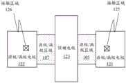
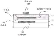
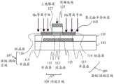
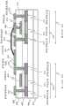
图3示意性地示出了本说明书的一个实施方式中的氧化物半导体TFT的配置示例。图3中的氧化物半导体TFT的配置示例包括顶栅电极123和底栅电极133。该氧化物半导体TFT可应用于驱动晶体管和开关晶体管两者。FIG. 3 schematically shows a configuration example of an oxide semiconductor TFT in one embodiment of the present specification. The configuration example of the oxide semiconductor TFT in FIG. 3 includes a
在使用该氧化物半导体TFT作为驱动晶体管的情况下,可以将用于控制沟道的电位供应给底栅电极133,并且可以将恒定电位供应给顶栅电极123。在使用该氧化物半导体TFT作为开关晶体管的情况下,可以将用于控制沟道的电位供应给顶栅电极123,并且可以将恒定电位供应给底栅电极133。在使用该氧化物半导体TFT作为开关晶体管的情况下,可以去除底栅电极133。In the case of using this oxide semiconductor TFT as a driving transistor, a potential for controlling a channel can be supplied to the
氧化物半导体TFT制造在由树脂或玻璃制成的柔性或刚性的绝缘基板101上。氧化物半导体TFT包括底栅电极133和位于底栅电极133与氧化物半导体层102之间的下绝缘层135。可以在底栅电极133与绝缘基板101之间设置未示出的绝缘层。底栅电极133由导体制成,例如具有高熔点的金属,例如W、Mo和Ta或其合金。The oxide semiconductor TFT is fabricated on a flexible or rigid insulating
氧化物半导体层102包括源极/漏极区域(S/D区域)105和107以及在面内方向上位于源极/漏极区域105与107之间的沟道区域103。下绝缘层135的一部分是位于底栅电极133与沟道区域103之间的底栅绝缘体。The
下绝缘层135可以是氧化硅层或者是氧化硅(上层)和氮化硅(下层)的堆叠体。氧化物半导体层102直接设置在下绝缘层135上方(与其接触)。源极/漏极区域105和107是电阻降低的区域。沟道区域103是电阻未降低的区域。稍后将描述电阻的降低。The lower
氧化物半导体层102可以由金属氧化物制成。金属氧化物的示例是氧化铟镓锌(IGZO)。The
氧化物半导体材料的其它示例包括具有高迁移率的材料(例如氧化铟镓锌锡(IGZTO)、氧化铟锌(IZO))和具有低迁移率的物质(例如氧化锌(ZnO))。Other examples of oxide semiconductor materials include materials with high mobility such as indium gallium zinc tin oxide (IGZTO), indium zinc oxide (IZO) and substances with low mobility such as zinc oxide (ZnO).
氧化物半导体层102包括下非晶层和上结晶层。具体地,沟道区域103由非晶层111和结晶层112组成;源极/漏极区域105由非晶层113和结晶层114组成;源极/漏极区域107由非晶层115和结晶层116组成。图3是示意图;非晶层和结晶层之间的实际界面不是平坦的,而是具有更复杂的几何形状。The
沟道区域103以及源极/漏极区域105和107具有相同的组成。每个区域中的非晶层和结晶层处于不同的有序状态,但它们的组成是相同的。
底栅电极133隔着下绝缘层135与沟道区域103相对。底栅电极133、下绝缘层135和沟道区域103从底部(更靠近基板的一侧)开始依次叠置。下绝缘层135部分地与沟道区域103和底栅电极133接触。下绝缘层135与沟道区域103和底栅电极133接触的部分对应于氧化物半导体TFT的底栅绝缘体。The
氧化物半导体TFT还包括顶栅电极123和在层叠方向上位于顶栅电极123与沟道区域103之间的上绝缘层117的区域。顶栅电极123由导体制成,例如具有高熔点的金属,例如W、Mo和Ta或其合金。The oxide semiconductor TFT also includes a
上绝缘层117覆盖氧化物半导体层102。上绝缘层117可以是氧化硅层、氮化硅层或它们的堆叠体。氧化物半导体层102、上绝缘层117和顶栅电极123从底部(更靠近基板的一侧)开始依次叠置。上绝缘层117与下绝缘层135、氧化物半导体层102和顶栅电极123接触。上绝缘层117的与顶栅电极123和沟道区域103接触的部分对应于顶栅绝缘体。The upper insulating
在使用氧化物半导体TFT作为驱动晶体管的情况下,用于控制到OLED元件的驱动电流的数据信号(信号电压)被供应给底栅电极133。顶栅电极123被供应恒定电位或保持在电浮动状态。在使用氧化物半导体TFT作为开关晶体管的情况下,用于使晶体管导通/截止的控制信号被供应给顶栅电极123。底栅电极133被供应恒定电位或保持在电浮动状态。替选地,可以去除底栅电极133。如稍后将描述的,顶栅电极123用作掩模以降低源极/漏极区域105和107的电阻(自对准)。In the case of using an oxide semiconductor TFT as a driving transistor, a data signal (signal voltage) for controlling a driving current to the OLED element is supplied to the
氧化物半导体TFT包括在顶栅电极123上方的层间绝缘层118。层间绝缘层118覆盖顶栅电极123并与顶栅电极123和上绝缘层117接触。层间绝缘层118可以是硅绝缘层或不同绝缘材料的多层结构。The oxide semiconductor TFT includes an interlayer insulating
氧化物半导体TFT包括在面内方向上夹置顶栅电极123的源极/漏极电极121和122。源极/漏极电极121和122由导体制成;例如,它们可以是单个铝层或Ti/Al/Ti的多层结构。The oxide semiconductor TFT includes source/
源极/漏极电极121包括延伸穿过层间绝缘层118和上绝缘层117的接触区域125。接触区域125在穿过层间绝缘层118和上绝缘层117开设的接触孔中与源极/漏极区域105接触(直接连接到源极/漏极区域105)。The source/
源极/漏极电极122包括延伸穿过层间绝缘层118和上绝缘层117的接触区域126。接触区域126在穿过层间绝缘层118和上绝缘层117开设的接触孔中与源极/漏极区域107接触(直接连接到源极/漏极区域107)。The source/
接触区域125和126在平面图中延伸穿过顶栅电极123外侧的区域中的层间绝缘层118和上绝缘层117,并且在平面图中不与顶栅电极123重叠。源极/漏极电极121和122的顶部区域与层间绝缘层118的顶面直接接触。在图3的配置示例中,源极/漏极电极121和122被设置成在平面图中不与顶栅电极123重叠。Contact
图4是示意性示出图3所示的氧化物半导体TFT的顶面的结构的平面图。图4示出了氧化物半导体TFT在平面图中的外观(当沿层叠方向观察时)。如图4所示,当从上方平面地观察时,源极/漏极电极121和122位于顶栅电极123的外侧而没有重叠。FIG. 4 is a plan view schematically showing the structure of the top surface of the oxide semiconductor TFT shown in FIG. 3 . FIG. 4 shows the appearance of an oxide semiconductor TFT in a plan view (when viewed in the stacking direction). As shown in FIG. 4 , the source/
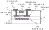
图5示意性地示出了本说明书的另一实施方式中的氧化物半导体TFT的配置示例。主要描述与图3中的配置示例的不同之处。上绝缘层127被蚀刻并且在平面图中不覆盖源极/漏极区域105和107。上绝缘层127覆盖沟道区域103。上绝缘层127的一部分或全部对应于位于沟道区域103与顶栅电极123之间的顶栅绝缘体。FIG. 5 schematically shows a configuration example of an oxide semiconductor TFT in another embodiment of the present specification. Differences from the configuration example in Fig. 3 are mainly described. The upper insulating
源极/漏极区域105和107从上绝缘层127暴露到层间绝缘层128。层间绝缘层128接触并覆盖源极/漏极区域105和107。源极/漏极电极121的接触区域125延伸穿过层间绝缘层128,并且在层间绝缘层128的孔中与源极/漏极区域105接触(直接连接到源极/漏极区域105)。源极/漏极电极122的接触区域126延伸穿过层间绝缘层128,并且在层间绝缘层128的孔中与源极/漏极区域107接触(直接连接到源极/漏极区域107)。The source/
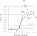
图6提供了具有图3所示配置的氧化物半导体TFT的顶栅特性和底栅特性的测量结果。在图6的曲线图中,横轴表示从顶栅电极或底栅电极施加的电场,纵轴表示漏极电流。曲线203表示顶栅特性,曲线201表示底栅特性。源极-漏极电压Vd为10V。FIG. 6 provides measurement results of top gate characteristics and bottom gate characteristics of the oxide semiconductor TFT having the configuration shown in FIG. 3 . In the graph of FIG. 6 , the horizontal axis represents the electric field applied from the top gate electrode or the bottom gate electrode, and the vertical axis represents the drain current.
底栅特性由漏极电流相对于底栅电极与氧化物半导体层之间的电场强度变化的变化来表示。在测量底栅特性时,顶栅电极处于浮动状态。顶栅特性由漏极电流相对于顶栅电极与氧化物半导体层之间的电场强度变化的变化来表示。在测量顶栅特性时,底栅电极处于浮动状态。The bottom gate characteristic is represented by a change in drain current with respect to a change in electric field strength between the bottom gate electrode and the oxide semiconductor layer. When measuring bottom gate characteristics, the top gate electrode is in a floating state. The top gate characteristic is represented by a change in drain current with respect to a change in electric field strength between the top gate electrode and the oxide semiconductor layer. When measuring top-gate characteristics, the bottom-gate electrode is in a floating state.
如图6所示,底栅驱动提供大的S值;与顶栅驱动相比,漏极电流的上升是平缓的。因此,在使用氧化物半导体TFT作为驱动晶体管时,底栅驱动是有利的。相比之下,顶栅驱动提供较小的S值;漏极电流的上升是急剧的。顶栅驱动提供了良好的开关特性,并且在使用氧化物半导体TFT作为开关晶体管时是有利的。As shown in Figure 6, the bottom gate drive provides a large S value; compared with the top gate drive, the rise of the drain current is gentle. Therefore, bottom gate driving is advantageous when using an oxide semiconductor TFT as a driving transistor. In contrast, top-gate drive provides a small S value; the rise in drain current is sharp. Top gate drive provides good switching characteristics and is advantageous when using an oxide semiconductor TFT as a switching transistor.
制造方法Manufacturing method
描述了制造氧化物半导体TFT的方法的示例。图7A至图7D示意性地示出了制造图3所示的氧化物半导体TFT的方法的示例。该方法穿过上绝缘层向氧化物半导体注入杂质,以降低源极/漏极区域的电阻。An example of a method of manufacturing an oxide semiconductor TFT is described. 7A to 7D schematically show an example of a method of manufacturing the oxide semiconductor TFT shown in FIG. 3 . The method implants impurities into an oxide semiconductor through an upper insulating layer to reduce the resistance of source/drain regions.
参考图7A,该制造方法在绝缘基板101上形成底栅电极133。该步骤通过溅射沉积金属层,并通过光刻和蚀刻形成底栅电极133。金属材料可以理想地选自例如Mo、W、Nb和Al。Referring to FIG. 7A , the manufacturing method forms a
此外,该制造方法通过化学气相沉积(CVD)沉积下绝缘层(例如,氧化硅层)135,随后形成氧化物半导体层102。氧化物半导体层102可以通过借助溅射沉积氧化物半导体并借助光刻图案化氧化物半导体膜来形成。In addition, the manufacturing method deposits a lower insulating layer (for example, a silicon oxide layer) 135 by chemical vapor deposition (CVD), and then forms the
形成氧化物半导体层102的步骤形成下非晶层151和上结晶层152。可以通过适当地确定溅射气体的状况来形成上结晶结构/下非晶结构。例如,溅射设备将氧气和氩气的混合气体引入其中放置氧化物半导体靶的腔室中。氧气与要引入的氧气和氩气的混合气体的比例(O2/(Ar+O2))可以在例如30%至60%的范围内。The step of forming the
在其上沉积氧化物半导体的基板与氧化物半导体靶之间施加高电压。可以采用任何溅射方案,例如DC溅射、RF溅射或磁控溅射。具有上结晶结构/下非晶结构的氧化物半导体层可以通过如上所述的用氧进行反应溅射来形成。A high voltage is applied between the substrate on which the oxide semiconductor is deposited and the oxide semiconductor target. Any sputtering scheme can be used, such as DC sputtering, RF sputtering or magnetron sputtering. The oxide semiconductor layer having an upper crystalline structure/lower amorphous structure can be formed by reactive sputtering with oxygen as described above.
接下来,该制造方法例如通过CVD沉积上绝缘层117。此后,该制造方法通过溅射沉积金属膜,并通过利用借助光刻而图案化的掩模蚀刻金属膜来形成顶栅电极123。金属材料可以理想地选自例如Mo、W、Nb和Al。Next, the manufacturing method deposits the upper insulating
参考图7B,该制造方法使用顶栅电极123作为掩模,穿过上绝缘层117向氧化物半导体层102注入杂质(例如,硼离子)。注入杂质离子在氧化物半导体层102中形成低电阻源极/漏极区域105和107。Referring to FIG. 7B , this manufacturing method implants impurities (for example, boron ions) into the
源极/漏极区域105和107是顶栅电极123外侧的区域;它们掺杂有杂质离子并且电阻降低。源极/漏极区域105由下非晶层113和上结晶层114组成,而源极/漏极区域107由下非晶层115和上结晶层116组成。注入杂质离子增加了源极/漏极区域105和107中的氧空位,并降低了那里的电阻。如稍后将描述的,注入杂质离子降低了源极/漏极区域105和107中的取向度,以降低那里的电阻。The source/
高电阻区域是沟道区域103。沟道区域103不暴露于杂质离子。因此,沟道区域103的下非晶层111和上结晶层112具有与杂质离子注入之前的下非晶层151和上结晶层152相同的特性。保持沟道区域103的高电阻。如上所述,通过使用顶栅电极123作为掩模的自对准来形成低电阻区域。The high resistance region is the
参考图7C,该制造方法沉积层间绝缘层118以覆盖顶栅电极123和上绝缘层117。层间绝缘层118可以通过例如借助CVD沉积氧化硅或氮化硅的一个或多个绝缘层来形成。Referring to FIG. 7C , the manufacturing method deposits an
参考图7D,该制造方法通过使用借助光刻而图案化的掩模蚀刻层间绝缘层118和上绝缘层117,在平面图中在顶栅电极123外侧的位置处开设穿过层间绝缘层118和上绝缘层117的接触孔。接触孔在不与顶栅电极123重叠的位置处穿透层间绝缘层118和上绝缘层117,以暴露氧化物半导体层102的源极/漏极区域105和107。Referring to FIG. 7D , the manufacturing method opens through the interlayer insulating
此外,该制造方法通过溅射沉积金属膜,并通过利用借助光刻而图案化的掩模蚀刻金属膜来形成源极/漏极电极121和122。源极/漏极电极121和122延伸穿过层间绝缘层118和上绝缘层117,并接触源极/漏极区域105和107的顶面。In addition, this manufacturing method deposits a metal film by sputtering, and forms the source/
接下来,描述制造氧化物半导体TFT的方法的另一示例。图8A至图8D示意性地示出了制造图5所示的氧化物半导体TFT的方法的示例。该方法将氧化物半导体的暴露区域暴露于等离子体以降低源极/漏极区域中的电阻。以下主要描述与参考图7A至图7D提供的描述的不同之处。Next, another example of a method of manufacturing an oxide semiconductor TFT is described. 8A to 8D schematically show an example of a method of manufacturing the oxide semiconductor TFT shown in FIG. 5 . This method exposes an exposed region of an oxide semiconductor to plasma to reduce resistance in source/drain regions. Differences from the description provided with reference to FIGS. 7A to 7D are mainly described below.
图8A与图7A基本相同;设置绝缘层141来代替上绝缘层117。绝缘层141的形状和形成与上绝缘层117的形状和形成相同。其他部件与图7A中的部件相同;它们可以通过与参照图7A描述的相同的方法来形成。FIG. 8A is basically the same as FIG. 7A ; an insulating
参考图8B,该制造方法通过使用顶栅电极123作为掩模蚀刻绝缘层141来形成上绝缘层127。因此,氧化物半导体层102被部分地暴露。该制造方法将氧化物半导体层102的暴露区域暴露于He等离子体以降低那里的电阻。由此形成低电阻的源极/漏极区域105和107。Referring to FIG. 8B , the manufacturing method forms an upper insulating
源极/漏极区域105和107的结构如参考图7B所述的一样。将源极/漏极区域105和107暴露于He等离子体会增加源极/漏极区域105和107中的氧空位,从而降低那里的电阻。如稍后将描述的,暴露于He等离子体降低了源极/漏极区域105和107中的取向度,以降低那里的电阻。The structure of the source/
高电阻区域是沟道区域103。沟道区域103不暴露于He等离子体。因此,沟道区域103的下非晶层111和上结晶层112具有与将源极/漏极区域105和107暴露于He等离子体之前的下非晶层151和上结晶层152相同的特性。保持沟道区域103的高电阻。如上所述,通过使用顶栅电极123作为掩模的自对准来形成低电阻区域。The high resistance region is the
参考图8C,该制造方法沉积层间绝缘层128以覆盖顶栅电极123和上绝缘层127。层间绝缘层128可以通过例如借助CVD沉积氧化硅或氮化硅的一个或多个绝缘层来形成。Referring to FIG. 8C , the manufacturing method deposits an
参考图8D,该制造方法通过利用借助光刻而图案化的掩模蚀刻层间绝缘层128,在平面图中在顶栅电极123外侧的位置处开设穿过层间绝缘层128的接触孔。接触孔在不与顶栅电极123重叠的位置处穿透层间绝缘层128,以暴露氧化物半导体层102的源极/漏极区域105和107。Referring to FIG. 8D , the manufacturing method opens a contact hole through interlayer insulating
此外,该制造方法通过溅射沉积金属膜,并通过利用借助光刻而图案化的掩模蚀刻金属膜来形成源极/漏极电极121和122。源极/漏极电极121和122延伸穿过层间绝缘层128并接触源极/漏极区域105和107的顶面。In addition, this manufacturing method deposits a metal film by sputtering, and forms the source/
在如上所述在像素电路中形成晶体管之后,制造OLED显示设备会形成OLED元件和结构封装单元。例如,在形成包括源极/漏极电极的金属层之后,该制造方法通过CVD沉积另一绝缘层(例如,氧化硅层),通过光刻和蚀刻形成钝化层,以及进一步沉积有机物质的外涂层。After the transistors are formed in the pixel circuit as described above, manufacturing an OLED display device forms OLED elements and structural encapsulation units. For example, after forming a metal layer including source/drain electrodes, the manufacturing method deposits another insulating layer (for example, a silicon oxide layer) by CVD, forms a passivation layer by photolithography and etching, and further deposits organic substances. outer coating.
接下来,该制造方法在外涂层上形成阳极电极,并通过穿过钝化层和外涂层开设的接触孔将每个阳极电极连接到源极/漏极区域。阳极电极的示例由透明导电膜、反射金属膜和另一透明导电膜这三层组成。透明导电材料可以是ITO或IZO。反射金属材料可以是Ag、Mg或Al。阳极电极可以通过溅射和蚀刻形成。Next, the fabrication method forms anode electrodes on the overcoat layer and connects each anode electrode to a source/drain region through a contact hole opened through the passivation layer and the overcoat layer. An example of the anode electrode is composed of three layers of a transparent conductive film, a reflective metal film, and another transparent conductive film. The transparent conductive material can be ITO or IZO. The reflective metal material can be Ag, Mg or Al. The anode electrode can be formed by sputtering and etching.
该制造方法还通过旋涂沉积光敏有机树脂膜,并将光敏有机树脂薄膜图案化以形成像素限定层。穿过像素限定层开设孔以暴露孔底部的阳极电极。像素限定层分离子像素的发光区域。该制造方法在每个阳极电极上沉积特定于红色、绿色或蓝色的有机发光材料,并且进一步在基板的整个区域上沉积阴极电极。此后,该制造方法形成结构封装单元。The manufacturing method also deposits a photosensitive organic resin film by spin coating, and patterns the photosensitive organic resin film to form a pixel defining layer. A hole is opened through the pixel defining layer to expose the anode electrode at the bottom of the hole. A pixel defining layer separates the light emitting regions of the sub-pixels. The manufacturing method deposits an organic light-emitting material specific to red, green or blue on each anode electrode, and further deposits a cathode electrode on the entire area of the substrate. Thereafter, the manufacturing method forms a structural encapsulation unit.
电子衍射法的测量结果Measurement results by electron diffraction method
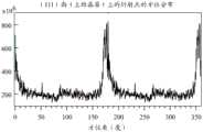
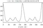
描述在本说明书的一个实施方式中通过电子衍射法从氧化物半导体TFT获得的测量结果。电子衍射测量使用透射电子显微镜(TEM)。该测量用电子束照射氧化物半导体TFT的氧化物半导体层以获得衍射图案,并生成衍射图案数据和方位分布图,这将在下文中描述。测量结果表明,氧化物半导体层由下非晶层和上结晶层组成,此外,低电阻区域(源极/漏极区域)中的取向度低于高电阻区域(沟道区域)中的取向度。A measurement result obtained from an oxide semiconductor TFT by an electron diffraction method in one embodiment of the present specification is described. Electron diffraction measurements use a transmission electron microscope (TEM). This measurement irradiates the oxide semiconductor layer of the oxide semiconductor TFT with an electron beam to obtain a diffraction pattern, and generates diffraction pattern data and an azimuth map, which will be described later. The measurement results showed that the oxide semiconductor layer was composed of a lower amorphous layer and an upper crystalline layer, and furthermore, the degree of orientation in the low-resistance region (source/drain region) was lower than that in the high-resistance region (channel region) .
图9A和图9B提供了通过电子衍射法从通过参考图7A至图7D所述的方法制造的样品获得的测量结果。图9A提供了上结晶层的(111)面上的衍射点的方位分布。图9B提供了下非晶层的(111)面上的衍射点的方位分布。这些轮廓表示从如图9C和图9D所示的TEM图像获得的傅里叶变换后的图像(其等同于衍射电子束的图像)中衍射点强度的方位依赖性。与这些傅里叶变换后的图像相比,在上结晶层中清晰地观察到更亮的衍射点。这两个图的横轴表示方位角,纵轴表示电子衍射的强度。图9A和图9B提供了在具有70nm厚度的氧化物半导体层中的40nm×40nm窄横截面区域的测量结果。9A and 9B provide measurements obtained by electron diffraction from samples fabricated by the method described with reference to FIGS. 7A to 7D . Figure 9A provides the azimuthal distribution of diffraction spots on the (111) plane of the upper crystalline layer. Figure 9B provides the azimuthal distribution of diffraction spots on the (111) plane of the lower amorphous layer. These profiles represent the azimuth dependence of the intensity of the diffraction spots in the Fourier-transformed image (which is equivalent to the image of the diffracted electron beam) obtained from the TEM images shown in FIGS. 9C and 9D . Compared to these Fourier-transformed images, brighter diffraction spots are clearly observed in the upper crystalline layer. The horizontal axis of these two figures represents the azimuth angle, and the vertical axis represents the intensity of electron diffraction. 9A and 9B provide measurement results of a 40 nm×40 nm narrow cross-sectional area in an oxide semiconductor layer having a thickness of 70 nm.
图9A中的上结晶层的测量结果具有高峰值。相比之下,图9B中的下非晶层的测量结果是平坦的,没有高峰值。这两个测量结果表明上层是结晶层,下层是非晶层。结晶层的峰值高于平均背景水平(200×106)的两倍。非晶层中的峰值的最高强度低于平均背景水平(200×106)的两倍。平均背景水平是指来自没有确定峰值的区域的信号的平均值。The measurement of the upper crystalline layer in FIG. 9A has a high peak. In contrast, the measurement of the lower amorphous layer in Fig. 9B is flat without high peaks. These two measurements indicate that the upper layer is crystalline and the lower layer is amorphous. The peak of the crystalline layer is twice the average background level (200×106 ). The highest intensity of the peak in the amorphous layer is less than twice the average background level (200×106 ). The mean background level refers to the mean value of the signal from the area without a defined peak.
图10A和图10B提供了通过电子衍射法从通过参考图7A至图7D描述的方法制造的样品获得的测量结果。图10A提供了在沟道区域的(111)面上的衍射点的方位分布。图10B提供了源极/漏极区域的(111)面上的衍射点的方位分布。这两个图的横轴表示方位角,纵轴表示电子衍射的强度。图10A和图10B提供了在具有70nm厚度的氧化物半导体层中的70nm×0.7μm的相对大的横截面区域的测量结果。10A and 10B provide measurement results obtained by electron diffraction from samples fabricated by the method described with reference to FIGS. 7A to 7D . Figure 10A provides the azimuthal distribution of diffraction spots on the (111) plane of the channel region. Figure 10B provides the azimuthal distribution of the diffraction spots on the (111) planes of the source/drain regions. The horizontal axis of these two figures represents the azimuth angle, and the vertical axis represents the intensity of electron diffraction. 10A and 10B provide measurement results of a relatively large cross-sectional area of 70 nm×0.7 μm in an oxide semiconductor layer having a thickness of 70 nm.
根据图10A中的测量结果计算的(111)取向度为17.2。根据图10B中的测量结果计算的(111)取向度为13.7。源极/漏极区域中的这种较低取向度表明源极/漏极区域的电阻适当降低。非晶氧化物半导体的取向度为1。取向度由方位分布中峰值强度的大小表示。The degree of (111) orientation calculated from the measurement results in FIG. 10A was 17.2. The degree of (111) orientation calculated from the measurement results in FIG. 10B was 13.7. This lower degree of orientation in the source/drain region indicates an appropriate reduction in the resistance of the source/drain region. The degree of orientation of the amorphous oxide semiconductor is 1. The degree of orientation is represented by the magnitude of the peak intensity in the azimuth distribution.
沟道区域和源极/漏极区域的窄区域中的取向度可以是与上述值不同的值。换言之,沟道区域(高电阻区域)的窄区域可以呈现出高取向度,而源极/漏极区域(低电阻区域)的窄区域可以呈现出低取向度。发明人的研究表明,当沟道区域和源极/漏极区域的横截面区域的面积大于氧化物半导体膜的厚度×0.5μm时,沟道区域呈现出高取向度,源极/漏极区域适当地呈现出低取向度。The degree of orientation in narrow regions of the channel region and source/drain regions may be a value different from the above-mentioned values. In other words, a narrow region of the channel region (high resistance region) can exhibit a high degree of orientation, while a narrow region of the source/drain region (low resistance region) can exhibit a low degree of orientation. The inventors' studies have shown that when the area of the cross-sectional area of the channel region and the source/drain region is larger than the thickness of the oxide semiconductor film × 0.5 μm, the channel region exhibits a high degree of orientation, and the source/drain region Appropriately exhibits a low degree of orientation.
设备结构equipment structure
描述包括多个氧化物半导体TFT的电路的一些结构示例。图11示出了像素电路的结构示例,该像素电路包括具有不同S值的开关氧化物半导体TFT(以下,也简称为开关TFT)和驱动氧化物半导体TFT(以下,也简称为驱动TFT)。Some structural examples of circuits including a plurality of oxide semiconductor TFTs are described. 11 shows a structural example of a pixel circuit including switching oxide semiconductor TFTs (hereinafter, also simply referred to as switching TFTs) and driving oxide semiconductor TFTs (hereinafter, also simply referred to as driving TFTs) having different S values.
图11示意性地示出了开关TFT和驱动TFT的横截面结构的示例。开关TFT310和驱动TFT 330被制造在由树脂或玻璃制成的柔性或刚性绝缘基板325上。开关TFT 310是第一氧化物半导体TFT,驱动TFT 330是第二氧化物半导体TFT。开关TFT 310具有这样的配置,使得底栅电极从参考图3描述的配置中去除。驱动TFT 330具有参考图3描述的配置。TFT 310和330可以通过参考图7A至图7D描述的方法一起制造。FIG. 11 schematically shows an example of the cross-sectional structures of a switching TFT and a driving TFT. The switching TFT 310 and the driving TFT 330 are fabricated on a flexible or rigid insulating
驱动TFT 330包括底栅电极337和位于底栅电极337上方的氧化物半导体层338。下绝缘层326设置在底栅电极337与氧化物半导体层338之间。氧化物半导体层338包括源极/漏极区域331和332以及在面内方向上位于源极/漏极区331与332之间的沟道区域333。The driving TFT 330 includes a
氧化物半导体层338设置在下绝缘层326上方并与下绝缘层326直接接触。源极/漏极区域331和332是电阻降低的氧化物半导体的区域。沟道区域333是电阻未降低的氧化物半导体的区域。如参考图3所述的,源极/漏极区域331和332以及沟道区域333各自由下非晶层和上结晶层组成。The
底栅电极337隔着下绝缘层326与沟道区域333相对。下绝缘层326与沟道区域333和底栅电极337直接接触。底栅电极337被供应数据信号并控制到OLED元件的驱动电流。The
驱动TFT 330还包括顶栅电极336。上绝缘层327设置在顶栅电极336与氧化物半导体层338之间。氧化物半导体层338、上绝缘层327、和顶栅电极336从底部(更靠近基板的一侧)开始依次叠置;上绝缘层327与氧化物半导体层338和顶栅电极336直接接触。The driving TFT 330 also includes a
设置层间绝缘层328以覆盖顶栅电极336和上绝缘层327。源极/漏极电极334和335延伸穿过层间绝缘层328和上绝缘层327,并直接连接到源极/漏极区域331和332。源极/漏极电极334和335的顶部区域与层间绝缘层328的顶面直接接触。将源极/漏极电极334与335中要被提供较低电位的电极334连接到OLED元件(图11中未示出)的阳极电极。An interlayer insulating
源极/漏极电极334和335分别包括在平面图中在顶栅电极336外侧的位置处向下延伸的接触区域339和340。接触区域339延伸穿过层间绝缘层328和上绝缘层327,并与源极/漏极区域331直接接触。接触区域340延伸穿过层间绝缘层328和上绝缘层327,并与源极/漏极区域332直接接触。The source/
源极/漏极电极334和顶栅电极336通过互连区域341连接。因此,这些电极保持在相同的电位。互连区域341从源极/漏极电极334延续,并且它们可以同时由相同的材料制成。互连区域341直接连接到顶栅电极336。互连区域341包括接触区域342,该接触区域342延伸穿过层间绝缘层328并与顶栅电极336的顶面直接接触。源极/漏极电极334可以被供应源极电位。顶栅电极336经由互连区域341连接到源极/漏极电极334,并且其电位等于源极/漏极电极334的电位。The source/
在平面图中,开关TFT 310设置在与驱动TFT 330的位置不同的位置处。开关TFT310包括氧化物半导体层318。氧化物半导体层318设置在下绝缘层326上方并与下绝缘层326直接接触。氧化物半导体层318包括源极/漏极区域311和312以及在面内方向上位于源极/漏极区域311与312之间的沟道区域313。In plan view, the switching TFT 310 is disposed at a position different from that of the driving TFT 330 . The switching TFT 310 includes an
源极/漏极区域311和312是电阻降低的氧化物半导体的区域。沟道区域313是电阻未降低的氧化物半导体的区域。如参考图3所述的,源极/漏极区域311和312以及沟道区域313各自由下非晶层和上结晶层组成。The source/
开关TFT 310还包括顶栅电极316。上绝缘层327位于顶栅电极316与氧化物半导体层318之间。氧化物半导体层318、上绝缘层327和顶栅电极316从底部(更靠近基板的一侧)开始依次叠置;上绝缘层327与氧化物半导体层318和顶栅电极316直接接触。顶栅电极316被供应用于使开关TFT 310导通/截止的控制信号。The switching TFT 310 also includes a
层间绝缘层328覆盖顶栅电极316和上绝缘层327。源极/漏极电极314和315延伸穿过层间绝缘层328和上绝缘层327,并直接连接到源极/漏极区域311和312。源极/漏极电极314和315的顶部区域与层间绝缘层328的顶面直接接触。The interlayer insulating
源极/漏极电极314和315分别包括在平面图中在顶栅电极316外侧的位置处向下延伸的接触区域319和320。接触区域319延伸穿过层间绝缘层328和上绝缘层327,并与源极/漏极区域311直接接触。接触区域320延伸穿过层间绝缘层328和上绝缘层327,并与源极/漏极区域312直接接触。The source/
开关TFT 310的源极/漏极电极314和驱动TFT 330的底栅电极337通过互连区域323连接。互连区域323从源极/漏极区域314延续,并且它们可以同时由相同的材料制成。互连区域323直接连接到底栅电极337。The source/
互连区域323包括接触区域324,该接触区域324延伸穿过层间绝缘层328、上绝缘层327和下绝缘层326,并且与从底栅电极337延伸的区域321的顶面直接接触。底栅电极337经由互连区域323连接到源极/漏极电极314,并且其电位等于源极/漏极电极314的电位。
图12示出了包括具有不同S值的开关TFT和驱动TFT的像素电路的结构示例。主要描述与图11中的配置示例的不同之处。图12示意性地示出了开关TFT和驱动TFT的横截面结构的示例。开关TFT 350和驱动TFT 370被制造在由树脂或玻璃制成的柔性或刚性绝缘基板325上。开关TFT 350具有这样的配置,使得底栅电极从参考图5描述的配置中去除。驱动TFT370具有参考图5描述的配置。TFT 350和370可以通过参考图8A至图8D描述的方法一起制造。FIG. 12 shows a configuration example of a pixel circuit including switching TFTs and driving TFTs having different S values. Differences from the configuration example in Fig. 11 are mainly described. FIG. 12 schematically shows an example of the cross-sectional structures of a switching TFT and a driving TFT. The switching
与图11中的配置示例相比,图12中的示例包括驱动TFT 370的顶栅绝缘体365和开关TFT 350的顶栅绝缘体367,以代替上绝缘层327。顶栅绝缘体365和367可以通过蚀刻绝缘层一起形成。顶栅绝缘体365位于顶栅电极336与沟道区域333之间,并且在平面图中不与源极/漏极区域331和332重叠。顶栅绝缘体367位于顶栅电极316与沟道区域313之间,并且在平面图中不与源极/漏极区域311和312重叠。Compared with the configuration example in FIG. 11 , the example in FIG. 12 includes the
代替层间绝缘层328,设置层间绝缘膜368。层间绝缘层368直接接触并覆盖源极/漏极区域311、312、331和332。在开关TFT 350中,源极/漏极电极314的接触区域319延伸穿过层间绝缘层368,并且在层间绝缘层368的孔中与源极/漏极区域311接触(直接连接到源极/漏极区域311)。源极/漏极电极315的接触区域320延伸穿过层间绝缘层368,并且在层间绝缘层368的孔中与源极/漏极区域312接触(直接连接到源极/漏极区域312)。Instead of the interlayer insulating
在驱动TFT 370中,源极/漏极电极334的接触区域339延伸穿过层间绝缘层368,并且在层间绝缘层368的孔中与源极/漏极区域331接触(直接连接到源极/漏极区域331)。源极/漏极电极335的接触区域340延伸穿过层间绝缘层368,并且在层间绝缘层368的孔中与源极/漏极区域332接触(直接连接到源极/漏极区域332)。In the driving TFT 370, the
图13示出了包括两个TFT的电路的结构示例。第一TFT和第二TFT具有与图11中的开关TFT 310相同的结构。图13中的配置示例使用电阻降低的氧化物作为线。具体地,第一TFT 410的源极/漏极区域和第二TFT 430的源极/漏极区域通过电阻降低的氧化物半导体的线(线区域)440连接。这种配置消除了源极/漏极区域与金属电极之间的接触电阻。TFT410和430分别对应于第一氧化物半导体TFT和第三氧化物半导体TFT;它们可以通过参考图7A至图7D描述的方法一起制造。FIG. 13 shows a structural example of a circuit including two TFTs. The first TFT and the second TFT have the same structure as the switching TFT 310 in FIG. 11 . The configuration example in FIG. 13 uses a resistance-reduced oxide as a line. Specifically, the source/drain region of the first TFT 410 and the source/drain region of the second TFT 430 are connected by a wire (wire region) 440 of an oxide semiconductor with reduced resistance. This configuration eliminates contact resistance between the source/drain regions and the metal electrodes. The TFTs 410 and 430 correspond to the first oxide semiconductor TFT and the third oxide semiconductor TFT, respectively; they can be manufactured together by the method described with reference to FIGS. 7A to 7D .
第一TFT 410和第二TFT 430位于设置在基板425上的下绝缘层426上方。在平面图中,第一TFT 410设置在与第二TFT 430的位置不同的位置处。The first TFT 410 and the second TFT 430 are located over the lower insulating
第一TFT 410包括氧化物半导体层418。氧化物半导体层418包括源极/漏极区域411和412以及在面内方向上位于源极/漏极区域411与412之间的沟道区域413。The first TFT 410 includes an
源极/漏极区域411和412是电阻降低的氧化物半导体的区域。沟道区域413是电阻未降低的氧化物半导体的区域。源极/漏极区域411和412以及沟道区域413各自由下非晶层和上结晶层组成。The source/
第一TFT 410包括顶栅电极416。上绝缘层427设置在顶栅电极416与氧化物半导体层418之间。氧化物半导体层418、上绝缘层427和顶栅电极416从底部(更靠近基板的一侧)开始依次叠置;上绝缘层427与氧化物半导体层418和顶栅电极416直接接触。例如,顶栅电极416被供应用于使第一TFT 410导通/截止的控制信号。The first TFT 410 includes a
设置层间绝缘层428以覆盖顶栅电极416和上绝缘层427。源极/漏极电极415延伸穿过层间绝缘层428和上绝缘层427,并直接连接到源极/漏极区域412。源极/漏极电极415的顶部区域与层间绝缘层428的顶面直接接触。An interlayer insulating
源极/漏极电极415包括在平面图中在顶栅电极416外侧的位置处向下延伸的接触区域420。接触区域420延伸穿过层间绝缘层428和上绝缘层427,并与源极/漏极区域412直接接触。The source/
第二TFT 430包括氧化物半导体层438。氧化物半导体层438包括源极/漏极区域431和432以及在面内方向上位于源极/漏极区域431与432之间的沟道区域433。The second TFT 430 includes an
源极/漏极区域431和432是电阻降低的氧化物半导体的区域。沟道区域433是电阻未降低的氧化物半导体的区域。源极/漏极区域431和432以及沟道区域433各自由下非晶层和上结晶层组成。The source/
第二TFT 430包括顶栅电极436。上绝缘层427位于顶栅电极436与氧化物半导体层438之间。氧化物半导体层438、上绝缘层427和顶栅电极436从底部(更靠近基板的一侧)开始依次叠置;上绝缘层427与氧化物半导体层438和顶栅电极436直接接触。例如,顶栅电极436被供应用于使第二TFT 430导通/截止的控制信号。The second TFT 430 includes a
层间绝缘层428覆盖顶栅电极436和上绝缘层427。源极/漏极电极435延伸穿过层间绝缘层428和上绝缘层427,并直接连接到源极/漏极区域432。源极/漏极电极435的顶部区域与层间绝缘层428的顶面直接接触。The interlayer insulating
源极/漏极电极435包括在顶栅电极436外侧的位置处向下延伸的接触区域442。接触区域442延伸穿过层间绝缘层428和上绝缘层427,并与源极/漏极区域432直接接触。The source/drain electrode 435 includes a
第一TFT 410的氧化物半导体层418和第二TFT 430的氧化物半导体层438是未分离的半导体膜的一部分,并且线(线区域)440位于它们之间。线440由电阻降低的氧化物半导体制成。氧化物半导体层418的源极/漏极区域411、线440和氧化物半导体层438的源极/漏极区域431未分离,并且它们同时由相同的材料制成。The
例如,制造步骤使用顶栅电极416和436作为掩模穿过上绝缘层427向氧化物半导体注入杂质离子,以一起形成源极/漏极区域411、线440和源极/漏极区域431。如上所述,第一TFT 410和第二TFT 430通过由电阻降低的氧化物半导体制成的线440串联连接。这种配置实现了氧化物半导体与TFT中的金属之间的低接触电阻。For example, the manufacturing step implants impurity ions into the oxide semiconductor through the upper insulating
图14示出了包括两个TFT的电路的结构示例。第一TFT 450和第二TFT 470具有与图11中的开关TFT 310相同的结构。第一TFT 450和第二TFT 470分别对应于第一氧化物半导体TFT和第四氧化物半导体TFT。图14中的配置示例将一个TFT的源极输出连接到另一TFT的顶栅电极。后一TFT的结晶沟道的栅极由前一TFT的源极输出驱动以加速操作。该配置适用于驱动器31和32中的连接以及驱动器31或32的输出到像素电路中的TFT的栅极的连接。FIG. 14 shows a structural example of a circuit including two TFTs. The first TFT 450 and the second TFT 470 have the same structure as the switching TFT 310 in FIG. 11 . The first TFT 450 and the second TFT 470 correspond to a first oxide semiconductor TFT and a fourth oxide semiconductor TFT, respectively. The configuration example in Fig. 14 connects the source output of one TFT to the top gate electrode of another TFT. The gate of the crystalline channel of the latter TFT is driven by the source output of the former TFT to speed up the operation. This configuration is applicable to the connection in the
第一TFT 450和第二TFT 470被制造在绝缘基板465上。TFT 450和470具有这样的配置,使得底栅电极被从参考图3描述的配置中去除。TFT 450和470可以通过参考图7A至图7D描述的方法一起制造。The first TFT 450 and the second TFT 470 are fabricated on the insulating
第一TFT 450和第二TFT 470位于设置在绝缘基板465上的下绝缘层466上方。在平面图中,第一TFT 450设置在与第二TFT 470的位置不同的位置处。The first TFT 450 and the second TFT 470 are located over the lower insulating
第一TFT 450包括氧化物半导体层458。氧化物半导体层458设置在下绝缘层466上方并与下绝缘层466直接接触。氧化物半导体层458包括源极/漏极区域451和452以及在面内方向上位于源极/漏极区域451与452之间的沟道区域453。The first TFT 450 includes an
源极/漏极区域451和452是电阻降低的氧化物半导体的区域。沟道区域453是电阻未降低的氧化物半导体的区域。如参考图3所述的,源极/漏极区域451和452以及沟道区域453各自由下非晶层和上结晶层组成。The source/
第一TFT 450还包括顶栅电极456。上绝缘层467位于顶栅电极456与氧化物半导体层458之间。氧化物半导体层458、上绝缘层467和顶栅电极456从底部(更靠近基板的一侧)开始依次叠置;上绝缘层467与氧化物半导体层458和顶栅电极456直接接触。例如,顶栅电极456被供应用于使第一TFT 450导通/截止的控制信号。The first TFT 450 also includes a
设置层间绝缘层468以覆盖顶栅电极456和上绝缘层467。源极/漏极电极454和455延伸穿过层间绝缘层468和上绝缘层467,并分别直接连接到源极/漏极区域451和452。源极/漏极电极454和455的顶部区域与层间绝缘层468的顶面直接接触。An interlayer insulating
源极/漏极电极454和455分别包括在平面图中在顶栅电极456外侧的位置处向下延伸的接触区域459和460。接触区域459延伸穿过层间绝缘层468和上绝缘层467,并与源极/漏极区域451直接接触。接触区域460延伸穿过层间绝缘层468和上绝缘层467,并与源极/漏极区域452直接接触。The source/
第二TFT 470包括氧化物半导体层478。氧化物半导体层478设置在下绝缘层466上方并与下绝缘层466直接接触。氧化物半导体层478包括源极/漏极区域471和472以及在面内方向上位于源极/漏极区域471与472之间的沟道区域473。The second TFT 470 includes an
源极/漏极区域471和472是电阻降低的氧化物半导体的区域。沟道区域473是电阻未降低的氧化物半导体的区域。如参考图3所述的,源极/漏极区域471和472以及沟道区域473各自由下非晶层和上结晶层组成。The source/
第二TFT 470还包括顶栅电极476。上绝缘层467位于顶栅电极476与氧化物半导体层478之间。氧化物半导体层478、上绝缘层467和顶栅电极476从底部(更靠近基板的一侧)开始依次叠置;上绝缘层467与氧化物半导体层478和顶栅电极476直接接触。例如,顶栅电极476被供应用于使第二TFT 470导通/截止的控制信号。The second TFT 470 also includes a top gate electrode 476 . The upper insulating
层间绝缘层468覆盖顶栅电极476和上绝缘层467。源极/漏极电极474和475延伸穿过层间绝缘层468和上绝缘层467,并分别直接连接到源极/漏极区域471和472。源极/漏极电极474和475的顶部区域与层间绝缘层468的顶面直接接触。The interlayer insulating
源极/漏极电极474和475分别包括在平面图中在顶栅电极456外侧的位置处向下延伸的接触区域479和480。接触区域479延伸穿过层间绝缘层468和上绝缘层467,并与源极/漏极区域471直接接触。接触区域480延伸穿过层间绝缘层468和上绝缘层467,并与源极/漏极区域472直接接触。The source/
第一TFT 450的源极/漏极电极454和第二TFT 470的顶栅电极476通过互连区域483连接。互连区域483从源极/漏极电极454延续,并且它们可以同时由相同的材料制成。互连区域483直接连接到顶栅电极476。The source/
互连区域483包括接触区域484,该接触区域484延伸穿过层间绝缘层468并与顶栅电极476的顶面直接接触。顶栅电极476经由互连区域483连接到源极/漏极电极454,并且其电位等于源极/漏极电极454的电位。
如上所述,已经描述了本发明的实施方式;然而,本发明不限于前述实施方式。本领域技术人员可以在本发明的范围内容易地修改、添加或转换前述实施方式中的每个元素。一个实施方式的配置的一部分可以替换为另一个实施方式的配置,或者一个实施方式的配置可以合并到另一个实施方式的配置中。As described above, the embodiments of the present invention have been described; however, the present invention is not limited to the aforementioned embodiments. Those skilled in the art can easily modify, add or convert each element in the foregoing embodiments within the scope of the present invention. A part of the configuration of one embodiment may be replaced with the configuration of another embodiment, or the configuration of one embodiment may be incorporated into the configuration of another embodiment.
Claims (14)
Applications Claiming Priority (2)
| Application Number | Priority Date | Filing Date | Title |
|---|---|---|---|
| JP2022-056684 | 2022-03-30 | ||
| JP2022056684AJP2023148580A (en) | 2022-03-30 | 2022-03-30 | Oxide semiconductor thin film transistor device and method for manufacturing the same |
Publications (1)
| Publication Number | Publication Date |
|---|---|
| CN116344552Atrue CN116344552A (en) | 2023-06-27 |
Family
ID=86881748
Family Applications (1)
| Application Number | Title | Priority Date | Filing Date |
|---|---|---|---|
| CN202310284050.6APendingCN116344552A (en) | 2022-03-30 | 2023-03-22 | Oxide semiconductor thin film transistor device and method of manufacturing the same |
Country Status (3)
| Country | Link |
|---|---|
| US (1) | US20230317732A1 (en) |
| JP (1) | JP2023148580A (en) |
| CN (1) | CN116344552A (en) |
Cited By (1)
| Publication number | Priority date | Publication date | Assignee | Title |
|---|---|---|---|---|
| WO2025043644A1 (en)* | 2023-08-31 | 2025-03-06 | 京东方科技集团股份有限公司 | Display substrate and manufacturing method therefor, and display apparatus |
Families Citing this family (1)
| Publication number | Priority date | Publication date | Assignee | Title |
|---|---|---|---|---|
| TWI855934B (en)* | 2023-11-30 | 2024-09-11 | 友達光電股份有限公司 | Semiconductor device and manufacturing method thereof |
Family Cites Families (5)
| Publication number | Priority date | Publication date | Assignee | Title |
|---|---|---|---|---|
| KR101316496B1 (en)* | 2006-08-23 | 2013-10-10 | 도요보 가부시키가이샤 | Polybenzazole fiber and pyridobisimidazole fiber |
| JP5389374B2 (en)* | 2008-04-23 | 2014-01-15 | 株式会社アドマテックス | Colored amorphous silica fine particles, production method thereof, and resin composition containing colored amorphous silica fine particles |
| US20130221345A1 (en)* | 2012-02-28 | 2013-08-29 | Semiconductor Energy Laboratory Co., Ltd. | Semiconductor device and method for manufacturing the same |
| CN109121438B (en)* | 2016-02-12 | 2022-02-18 | 株式会社半导体能源研究所 | Semiconductor device and display device including the same |
| WO2020075268A1 (en)* | 2018-10-11 | 2020-04-16 | 堺ディスプレイプロダクト株式会社 | Thin-film transistor and method for manufacturing same |
- 2022
- 2022-03-30JPJP2022056684Apatent/JP2023148580A/enactivePending
- 2023
- 2023-03-22CNCN202310284050.6Apatent/CN116344552A/enactivePending
- 2023-03-29USUS18/127,944patent/US20230317732A1/enactivePending
Cited By (1)
| Publication number | Priority date | Publication date | Assignee | Title |
|---|---|---|---|---|
| WO2025043644A1 (en)* | 2023-08-31 | 2025-03-06 | 京东方科技集团股份有限公司 | Display substrate and manufacturing method therefor, and display apparatus |
Also Published As
| Publication number | Publication date |
|---|---|
| JP2023148580A (en) | 2023-10-13 |
| US20230317732A1 (en) | 2023-10-05 |
Similar Documents
| Publication | Publication Date | Title |
|---|---|---|
| USRE49814E1 (en) | Transistor display panel, manufacturing method thereof, and display device including the same | |
| US8586979B2 (en) | Oxide semiconductor transistor and method of manufacturing the same | |
| US8384080B2 (en) | Thin film transistor, display device, and electronic device | |
| CN106992185B (en) | Thin film transistor substrate, display including the same, and manufacturing method thereof | |
| EP2086013A1 (en) | Oxide semiconductor transistor and method of manufacturing the same | |
| US9553201B2 (en) | Thin film transistor, thin film transistor array panel, and manufacturing method of thin film transistor | |
| CN114695387B (en) | Thin Film Transistor Substrate | |
| TW201714296A (en) | Array substrate, display device and preparation method of array substrate | |
| US20150162399A1 (en) | Semiconductor device, method of manufacturing the same, display unit, and electronic apparatus | |
| US20230317732A1 (en) | Oxide semiconductor thin-film transistor device and method of manufacturing the same | |
| US9608009B2 (en) | Display device and method of fabricating the same | |
| EP3101693A1 (en) | Thin-film transistor, pixel structure, manufacturing methods therefor, array substrate and display device | |
| CN107086227A (en) | Light emitting circuit, electronic device, thin film transistor and manufacturing method thereof | |
| US20110240986A1 (en) | Pixel structure of electroluminescent display panel and method of making the same | |
| JP7636159B2 (en) | Thin Film Devices | |
| CN104009043A (en) | Pixel structure and manufacturing method thereof | |
| US11398508B2 (en) | Thin-film device | |
| WO2016123979A1 (en) | Thin-film transistor and manufacturing method therefor, array substrate and display device | |
| JP2001100655A (en) | El display device | |
| CN115411057B (en) | Array substrate, manufacturing method thereof, and display device | |
| US20160149042A1 (en) | Semiconductor device and method of manufacturing the same, and display unit and electronic apparatus | |
| CN112714960B (en) | Display device | |
| JP7681958B2 (en) | Thin Film Transistor Circuit | |
| US20230178655A1 (en) | Oxide semiconductor thin-film transistor device and method of manufacturing the same | |
| CN203423187U (en) | Thin film transistor, array substrate, and display device |
Legal Events
| Date | Code | Title | Description |
|---|---|---|---|
| PB01 | Publication | ||
| PB01 | Publication | ||
| SE01 | Entry into force of request for substantive examination | ||
| SE01 | Entry into force of request for substantive examination |