CN116318644A - Error detecting device for data encryption - Google Patents
Error detecting device for data encryptionDownload PDFInfo
- Publication number
- CN116318644A CN116318644ACN202211207303.1ACN202211207303ACN116318644ACN 116318644 ACN116318644 ACN 116318644ACN 202211207303 ACN202211207303 ACN 202211207303ACN 116318644 ACN116318644 ACN 116318644A
- Authority
- CN
- China
- Prior art keywords
- key
- parity
- small
- circuit
- bits
- Prior art date
- Legal status (The legal status is an assumption and is not a legal conclusion. Google has not performed a legal analysis and makes no representation as to the accuracy of the status listed.)
- Pending
Links
Images


Classifications
- H—ELECTRICITY
- H04—ELECTRIC COMMUNICATION TECHNIQUE
- H04L—TRANSMISSION OF DIGITAL INFORMATION, e.g. TELEGRAPHIC COMMUNICATION
- H04L9/00—Cryptographic mechanisms or cryptographic arrangements for secret or secure communications; Network security protocols
- H04L9/08—Key distribution or management, e.g. generation, sharing or updating, of cryptographic keys or passwords
- H04L9/0816—Key establishment, i.e. cryptographic processes or cryptographic protocols whereby a shared secret becomes available to two or more parties, for subsequent use
- H—ELECTRICITY
- H04—ELECTRIC COMMUNICATION TECHNIQUE
- H04L—TRANSMISSION OF DIGITAL INFORMATION, e.g. TELEGRAPHIC COMMUNICATION
- H04L9/00—Cryptographic mechanisms or cryptographic arrangements for secret or secure communications; Network security protocols
- H04L9/08—Key distribution or management, e.g. generation, sharing or updating, of cryptographic keys or passwords
- H04L9/0861—Generation of secret information including derivation or calculation of cryptographic keys or passwords
- H04L9/0863—Generation of secret information including derivation or calculation of cryptographic keys or passwords involving passwords or one-time passwords
- H—ELECTRICITY
- H04—ELECTRIC COMMUNICATION TECHNIQUE
- H04L—TRANSMISSION OF DIGITAL INFORMATION, e.g. TELEGRAPHIC COMMUNICATION
- H04L9/00—Cryptographic mechanisms or cryptographic arrangements for secret or secure communications; Network security protocols
- H04L9/08—Key distribution or management, e.g. generation, sharing or updating, of cryptographic keys or passwords
- H04L9/088—Usage controlling of secret information, e.g. techniques for restricting cryptographic keys to pre-authorized uses, different access levels, validity of crypto-period, different key- or password length, or different strong and weak cryptographic algorithms
- Y—GENERAL TAGGING OF NEW TECHNOLOGICAL DEVELOPMENTS; GENERAL TAGGING OF CROSS-SECTIONAL TECHNOLOGIES SPANNING OVER SEVERAL SECTIONS OF THE IPC; TECHNICAL SUBJECTS COVERED BY FORMER USPC CROSS-REFERENCE ART COLLECTIONS [XRACs] AND DIGESTS
- Y02—TECHNOLOGIES OR APPLICATIONS FOR MITIGATION OR ADAPTATION AGAINST CLIMATE CHANGE
- Y02D—CLIMATE CHANGE MITIGATION TECHNOLOGIES IN INFORMATION AND COMMUNICATION TECHNOLOGIES [ICT], I.E. INFORMATION AND COMMUNICATION TECHNOLOGIES AIMING AT THE REDUCTION OF THEIR OWN ENERGY USE
- Y02D30/00—Reducing energy consumption in communication networks
- Y02D30/50—Reducing energy consumption in communication networks in wire-line communication networks, e.g. low power modes or reduced link rate
Landscapes
- Engineering & Computer Science (AREA)
- Computer Security & Cryptography (AREA)
- Computer Networks & Wireless Communication (AREA)
- Signal Processing (AREA)
- Storage Device Security (AREA)
- Detection And Correction Of Errors (AREA)
- Error Detection And Correction (AREA)
Abstract
Description
Translated fromChinese技术领域technical field
本发明涉及数据加密,特别是,本发明涉及一种数据加密的错误侦测装置。The present invention relates to data encryption, in particular, the present invention relates to a data encryption error detection device.
背景技术Background technique
由于现在的存储装置(例如,NAND闪存)常用于存储系统程序代码、应用程序代码、驱动程序和用户的隐私数据等,因此数据安全性是重要议题。高级加密标准(AdvancedEncryption Standard,AES)是目前由美国联邦政府采用的一种区块加密标准,并且已经被多方验证且广为采用。然而,AES运行的过程中可能遭到恶意的攻击,而让AES编码器错误的产生运算结果。或者是,芯片制作过程中有些瑕疵,使得AES编码器在运行一段时间后会产生不预期的运算结果。或者是,存储装置处在恶劣的环境下,让AES编码器中的部分元件失效而产生不预期的运算结果。错误的加密过程将使原始的用户数据无法恢复,造成巨大的损失。因此,本发明提出一种数据加密的错误侦测装置及方法,避免写入错误的加密后数据到存储装置。Since current storage devices (eg, NAND flash memory) are often used to store system program codes, application program codes, drivers, and user privacy data, data security is an important issue. Advanced Encryption Standard (AES) is a block encryption standard currently adopted by the US federal government, and has been verified by multiple parties and widely adopted. However, malicious attacks may occur during the operation of AES, and the AES encoder may generate incorrect calculation results. Or, there are some flaws in the chip manufacturing process, which makes the AES encoder produce unexpected calculation results after running for a period of time. Or, the storage device is in a harsh environment, causing some components in the AES encoder to fail and produce unexpected calculation results. A wrong encryption process will make the original user data irrecoverable and cause huge losses. Therefore, the present invention proposes a data encryption error detection device and method to avoid writing wrong encrypted data to a storage device.
发明内容Contents of the invention
有鉴于此,如何减轻或消除上述相关领域的缺失,实为有待解决的问题。In view of this, how to alleviate or eliminate the deficiencies in the above-mentioned related fields is a problem to be solved.
本发明涉及一种数据加密的错误侦测装置,包含:密钥产生电路;和密钥错误检查电路。密钥产生电路,设置以实现加密算法中的扩展密钥操作,用于使用基础密钥产生多个回合密钥,其中,所述加密算法使用一个所述回合密钥在相应回合中对明文或者中间加密结果进行编码。密钥错误检查电路设置以预测出相应于每个回合密钥的冗余数据;并且在扩展密钥过程中的指定中间点发现任何回合密钥和相应冗余数据不匹配时,发出错误信号给处理单元。The invention relates to an error detection device for data encryption, comprising: a key generating circuit; and a key error checking circuit. A key generation circuit, configured to implement extended key operations in an encryption algorithm, for generating a plurality of round keys using a basic key, wherein the encryption algorithm uses one of the round keys in a corresponding round for plaintext or Intermediate encryption results are encoded. key error checking circuitry arranged to predict redundant data corresponding to each round key; and to signal an error to processing unit.
本发明还涉及一种数据加密的错误侦测装置,包含:搜索电路;和替代校验电路。搜索电路设置以依据查找表将输入的相应于回合密钥的1个字节的第一值转换为第二值。替代校验电路设置以使用相应于查找表的公式判断第一值转换为第二值的过程中是否发生错误,以及当发现错误时,发出错误信号。The present invention also relates to an error detection device for data encryption, comprising: a search circuit; and a replacement check circuit. The search circuit is configured to convert the input first value of 1 byte corresponding to the round key into a second value according to the look-up table. The alternative verification circuit is configured to use a formula corresponding to the look-up table to determine whether an error occurs during conversion of the first value to the second value, and to send an error signal when an error is found.
上述实施例的优点之一,通过以上所述密钥错误检查电路的设置,可利用比密钥产生电路较少面积的电路来完成错误侦测。One of the advantages of the above-mentioned embodiment is that through the configuration of the above-mentioned key error checking circuit, the error detection can be completed with a circuit having a smaller area than the key generation circuit.
本发明的其他优点将配合以下的说明和说明书附图进行更详细的解说。。Other advantages of the present invention will be explained in more detail in conjunction with the following description and accompanying drawings. .
附图说明Description of drawings
此处所说明的说明书附图用来提供对本申请的进一步理解,构成本申请的一部分,本申请的示意性实施例及其说明用于解释本申请,并不构成对本申请的不当限定。The accompanying drawings described here are used to provide a further understanding of the application and constitute a part of the application. The schematic embodiments and descriptions of the application are used to explain the application and do not constitute an improper limitation to the application.
图1为依据本发明实施例的电子装置的系统架构图。FIG. 1 is a system architecture diagram of an electronic device according to an embodiment of the invention.
图2为依据本发明实施例的闪存模块的示意图。FIG. 2 is a schematic diagram of a flash memory module according to an embodiment of the invention.
图3为以128比特密钥使用10个回合的算法的高阶示意图。Figure 3 is a high-level schematic diagram of an algorithm using 10 rounds with a 128-bit key.
图4为依据一些实施方式的高级加密标准(Advanced Encryption Standard,AES)编码器的框图。4 is a block diagram of an Advanced Encryption Standard (AES) encoder in accordance with some implementations.
图5为依据本发明实施例的AES编码器的框图。FIG. 5 is a block diagram of an AES encoder according to an embodiment of the present invention.
图6为依据本发明实施例的体、体内奇偶校验比特和跨体奇偶校验9比特的示意图。FIG. 6 is a schematic diagram of a body, body parity bits, and
图7为依据本发明实施例的小钥、小钥内奇偶校验比特和跨小钥奇偶校验9比特的示意图。Fig. 7 is a schematic diagram of a small key, parity bits within a small key, and 9 bits of parity across small keys according to an embodiment of the present invention.
图8为依据本发明实施例的AES编码器的框图。FIG. 8 is a block diagram of an AES encoder according to an embodiment of the present invention.
图9为依据本发明实施例的AES数据处理电路的框图。FIG. 9 is a block diagram of an AES data processing circuit according to an embodiment of the present invention.
图10为依据本发明实施例的奇偶校验预测电路的框图。FIG. 10 is a block diagram of a parity prediction circuit according to an embodiment of the present invention.
图11为依据本发明实施例的体内奇偶校验比特预测电路的框图。FIG. 11 is a block diagram of an in-body parity bit prediction circuit according to an embodiment of the present invention.
图12为依据本发明实施例的体内奇偶校验比特产生电路的框图。FIG. 12 is a block diagram of an internal parity bit generating circuit according to an embodiment of the present invention.
图13为依据本发明实施例的跨体奇偶校验9比特预测电路的框图。FIG. 13 is a block diagram of a 9-bit prediction circuit for cross-body parity according to an embodiment of the present invention.
图14为依据本发明实施例的增强型替代字节电路的框图。FIG. 14 is a block diagram of an enhanced substitute byte circuit according to an embodiment of the present invention.
图15为依据本发明实施例的增强型查表电路的框图。FIG. 15 is a block diagram of an enhanced look-up table circuit according to an embodiment of the present invention.
图16为依据本发明实施例的替代校验电路的框图。FIG. 16 is a block diagram of an alternative verification circuit according to an embodiment of the present invention.
图17为依据本发明实施例的AES密钥调度电路的框图。FIG. 17 is a block diagram of an AES key scheduling circuit according to an embodiment of the present invention.
图18为依据本发明实施例的钥字处理电路的框图。FIG. 18 is a block diagram of a key word processing circuit according to an embodiment of the present invention.
图19为依据本发明实施例的替代钥字电路的框图。FIG. 19 is a block diagram of a substitute key circuit according to an embodiment of the present invention.
图20为依据本发明实施例的舍去常数电路的示意图。FIG. 20 is a schematic diagram of a rounding constant circuit according to an embodiment of the present invention.
图21为依据本发明实施例的钥字处理电路的框图。FIG. 21 is a block diagram of a key word processing circuit according to an embodiment of the present invention.
附图标记说明:Explanation of reference signs:
10 电子装置10 electronics
110 主机端110 host side
130 闪存控制器130 flash memory controller
131 主机接口131 host interface
132 总线132 bus
134 处理单元134 processing units
136 随机存取存储器136 Random Access Memory
137 高级加密标准编码器137 Advanced Encryption Standard Encoder
138 直接存储器存取控制器138 direct memory access controller
139 闪存接口139 Flash Interface
150 闪存模块150 flash modules
151 接口151 interface
153#0~153#15 NAND闪存单元153#0~153#15 NAND flash memory unit
CH#0~CH#3 通道
CE#0~CE#3 启动信号
R#0 初始回合
R#1~R#9 中间回合
R#10 最终回合
S310#1~S310#10 替代字节步骤
S320#1~S320#10 位移行步骤
S330#1~S330#9 混合列步骤
S340#1~S340#10 加上回合密钥步骤
S350 扩展密钥步骤S350 Extended Key Procedure
w[0,3] 基础密钥w[0,3] base key
w[4,7]、w[36,39]、w[40,43] 扩展后的密钥w[4,7], w[36,39], w[40,43] expanded keys
400 AES编码器400 AES Encoder
410、430 AES编码电路410, 430 AES encoding circuit
450 比较器450 Comparator
500 AES编码器500 AES Encoder
510 AES编码电路510 AES encoding circuit
530 错误侦测电路530 error detection circuit
550 冗余数据产生电路550 redundant data generating circuit
570 冗余密钥产生电路570 redundant key generation circuit
S0~S15 体S0 ~ S15 bodies
P0~P15 体内奇偶校验比特P0 ~ P15 internal parity bits
Q0~Q3 跨体奇偶校验9比特Q0 ~ Q3
k0~k31 小钥k0 ~k31 small key
R0~R31 小钥内奇偶校验比特R0 ~ R31 parity bits in the small key
V0~V7跨小钥奇偶校验9比特V0 ~ V7 across the small
810 AES数据处理电路810 AES data processing circuit
813 编码电路813 encoding circuit
815 编码错误检查电路815 encoding error checking circuit
830 AES密钥调度电路830 AES key scheduling circuit
833 密钥产生电路833 key generation circuit
835 密钥错误检查电路835 key error check circuit
850 或门850 OR gate
870 控制器870 controller
912 数据寄存器912 data register
914 奇偶校验码寄存器914 Parity register
920 增强型替代字节电路920 Enhanced Substitute Byte Circuit
930 位移行电路930-bit row circuit
940 混合列电路940 mixed column circuit
950 加上回合密钥电路950 plus round key circuit
960 奇偶校验检查电路960 parity check circuit
970 奇偶校验预测电路970 parity prediction circuit
980 复用器980 multiplexer
1010 体内奇偶校验比特预测电路1010 In-body parity bit prediction circuit
1030 跨体奇偶校验9比特预测电路1030 Span Parity 9-bit Prediction Circuit
1110 体内奇偶校验比特产生电路1110 internal parity bit generation circuit
1120 位移行预测电路1120-bit line prediction circuit
1130 混合列预测电路1130 Hybrid Column Prediction Circuit
1140 复用器1140 multiplexer
1150 加上回合密钥预测电路1150 plus round key prediction circuit
1160 位移行电路1160-bit row circuit
1210 复用器1210 multiplexer
1230 体内互斥或门1230 Internal exclusive OR gate
1310 跨体奇偶校验字节产生电路1310 Span Parity Byte Generation Circuit
1330 跨小钥奇偶校验字节分割电路1330 across small key parity byte segmentation circuit
1350 跨体奇偶校验字节预测电路1350 Span Parity Byte Prediction Circuit
1370 跨体奇偶校验1比特预测电路1370 Span Parity 1-bit Prediction Circuit
1390 跨体奇偶校验9比特合并电路1390 cross-body parity 9-bit merge circuit
1410 跨体奇偶校验字节分割电路1410 Span Parity Byte Segmentation Circuit
1430#0~1430#15 增强型查表电路1430#0~1430#15 enhanced look-up table circuit
1450 跨体奇偶校验字节合并电路1450 Span Parity Byte Merge Circuit
1510 搜索电路1510 search circuit
1530 替代校验电路1530 Alternative Calibration Circuit
1610 计算电路1610 computing circuits
1630 乘法器1630 multiplier
1650 比较器1650 Comparator
1710、1750 密钥分割电路1710, 1750 key split circuit
1712、1714 寄存器1712, 1714 registers
1720、1730 钥字处理电路1720, 1730 key word processing circuit
1725、1727、1729 互斥或门1725, 1727, 1729 exclusive OR gates
1742、1744 密钥奇偶校验码产生电路1742, 1744 key parity code generation circuit
1752、1754、1782、1784 寄存器1752, 1754, 1782, 1784 registers
1762、1764 密钥奇偶校验检查电路1762, 1764 key parity check circuit
1772、1774 密钥奇偶校验预测电路1772, 1774 key parity prediction circuit
1810 钥字分割电路1810 key word segmentation circuit
1820 旋转钥字电路1820 rotary key circuit
1830 替代钥字电路1830 Alternative key word circuit
1840 舍去常数电路1840 rounding constant circuit
1850 钥字合并电路1850 Key Word Merging Circuit
1860 钥字奇偶校验产生电路1860 Key Word Parity Generation Circuit
1870 钥字奇偶校验预测电路1870 Key Word Parity Prediction Circuit
1880 钥字跨奇偶校验预测电路1880 key word cross parity prediction circuit
1890 钥字奇偶校验9比特合并电路1890 keyword parity check 9-bit merging circuit
1930#0~1930#3 增强型查表电路1930#0~1930#3 enhanced look-up table circuit
2010 互斥或门2010 Exclusive OR Gate
2110 钥字分割电路2110 key word segmentation circuit
2130 替代钥字电路2130 Alternative key word circuit
2150 钥字合并电路2150 key combination circuit
2160 钥字奇偶校验产生电路2160 key word parity generation circuit
2180 钥字跨奇偶校验预测电路2180 key word cross parity prediction circuit
2190 钥字奇偶校验9比特合并电路2190 key word parity check 9-bit merge circuit
具体实施方式Detailed ways
以下将配合相关附图来说明本发明的实施例。在这些附图中,相同的标号表示相同或类似的组件或方法流程。Embodiments of the present invention will be described below in conjunction with related drawings. In these drawings, the same reference numerals represent the same or similar components or method flows.
必须了解的是,使用在本说明书中的“包含”、“包括”等词,是用于表示存在特定的技术特征、数值、方法步骤、作业处理、元件和/或组件,但并不排除可加上更多的技术特征、数值、方法步骤、作业处理、元件、组件,或以上的任意组合。It must be understood that words such as "comprising" and "including" used in this specification are used to indicate the existence of specific technical features, values, method steps, operation processes, components and/or components, but do not exclude possible Add more technical characteristics, values, method steps, operation processes, components, components, or any combination of the above.
本发明中使用如“第一”、“第二”、“第三”等词是用来修饰权利要求中的组件,并非用来表示之间具有优先权顺序,先行关系,或者是一个组件先于另一个组件,或者是执行方法步骤时的时间先后顺序,仅用来区别具有相同名字的组件。Words such as "first", "second", and "third" used in the present invention are used to modify the components in the claims, and are not used to indicate that there is a priority order, a prior relationship, or that a component is prior relative to another component, or the chronological order in which method steps are performed, is only used to distinguish components with the same name.
必须了解的是,当组件描述为“连接”或“耦接”至另一组件时,可以是直接连结、或耦接至其他组件,可能出现中间组件。相反地,当组件描述为“直接连接”或“直接耦接”至另一组件时,其中不存在任何中间组件。使用于描述组件之间关系的其他词语也可以类似方式解读,例如“介于”相对于“直接介于”,或者是“邻接”相对于“直接邻接”等等。It must be understood that when an element is referred to as being "connected" or "coupled" to another element, it can be directly connected or coupled to the other element, intervening elements may be present. In contrast, when a component is described as being "directly connected" or "directly coupled" to another component, there are no intervening components present. Other words used to describe the relationship between components may be read in a similar manner, such as "between" versus "directly between," or "adjacent" versus "directly adjacent," and so forth.
参考图1。电子装置10包含:主机端(Host Side)110、闪存控制器130及闪存模块150,并且闪存控制器130及闪存模块150可合称为装置端(Device Side)。电子装置10可实施于个人计算机、笔记本计算机(Laptop PC)、平板计算机、移动电话、数字相机、数字摄影机、智能型电视、智能型电冰箱、车用电子系统(Automotive Electronics System)等电子产品之中。主机端110与闪存控制器130的主机接口(Host Interface)131可以通用串行总线(Universal Serial Bus,USB)、先进技术附件(Advanced Technology Attachment,ATA)、串行先进技术附件(Serial Advanced Technology Attachment,SATA)、快速外设组件互联(Peripheral Component Interconnect Express,PCI-E)、通用闪存存储(Universal Flash Storage,UFS)、嵌入式多媒体卡(Embedded Multi-Media Card,eMMC)等通信协议彼此通信。闪存控制器130的闪存接口(Flash Interface)139与闪存模块150可以双倍数据率(Double Data Rate,DDR)通信协议彼此通信,例如,开放NAND闪存接口(OpenNAND Flash Interface,ONFI)、双倍数据率开关(DDR Toggle)或其他通信协议。闪存控制器130包含处理单元134,可使用多种方式实施,如使用通用硬件(例如,单处理器、具有并行处理能力的多处理器、图形处理器或其他具有运算能力的处理器),并且在执行软件以及/或固件指令时,提供之后描述的功能。处理单元134通过主机接口131接收主机命令,例如读取命令(Read Command)、写入命令(Write Command)、丢弃命令(Discard Command)、抹除命令(Erase Command)等,调度并执行这些命令。闪存控制器130还包含随机存取存储器(Random Access Memory,RAM)136,可实施为动态随机存取存储器(Dynamic RandomAccess Memory,DRAM)、静态随机存取存储器(Static Random Access Memory,SRAM)或上述两者的结合,用于配置空间作为数据缓冲区,存储从主机端110读取并即将写入闪存模块150的主机数据,以及从闪存模块150读取并即将输出给主机端110的主机数据。随机存取存储器136还可存储执行过程中需要的数据,例如,变量、数据表、主机-闪存对照表(Host-to-Flash,H2F Table)、闪存-主机对照表(Flash-to-Host,F2H Table)等。闪存接口139包含NAND闪存控制器(NAND Flash Controller,NFC)提供存取闪存模块150时需要的功能,例如命令串行器(Command Sequencer)、低密度奇偶校验(Low Density Parity Check,LDPC)等。Refer to Figure 1. The
闪存控制器130中可配置共享总线架构(Shared Bus Architecture)132,用于让组件之间彼此耦接以传递数据、地址、控制信号等,这些组件包含:主机接口131、处理单元134、RAM 136、高级加密标准(Advanced Encryption Standard,AES)编码器137、直接存储器存取(Direct Memory Access,DMA)控制器138、闪存接口139等。DMA控制器138可依据处理单元134的指令,通过总线架构132在元件间迁移数据,例如,将RAM136的特定数据缓存器中的数据搬到AES编码器137的特定寄存器(Register),将AES编码器137的特定寄存器中的数据搬到RAM136的特定数据缓存器等。A shared bus architecture (Shared Bus Architecture) 132 can be configured in the
闪存模块150提供大量的存储空间,通常是数百个千兆字节(Gigabytes,GB),甚至是多个万亿字节(Terabytes,TB),用于存储大量的用户数据,例如高分辨率图片、影片等。闪存模块150中包含控制电路以及存储器数组,存储器数组中的存储单元可在抹除后配置为单层式单元(Single Level Cells,SLCs)、多层式单元(Multiple Level Cells,MLCs)、三层式单元(Triple Level Cells,TLCs)、四层式单元(Quad-Level Cells,QLCs)或上述的任意组合。处理单元134通过闪存接口139写入用户数据到闪存模块150中的指定地址(目的地址),以及从闪存模块150中的指定地址(来源地址)读取用户数据。闪存接口139使用多个电子信号来协调闪存控制器130与闪存模块150间的数据与命令传递,包含数据线(DataLine)、时钟信号(Clock Signal)与控制信号(Control Signal)。数据线可用于传递命令、地址、读出及写入的数据;控制信号线可用于传递芯片启动(Chip Enable,CE)、地址提取启动(Address Latch Enable,ALE)、命令提取启动(Command Latch Enable,CLE)、写入启动(Write Enable,WE)等控制信号。The
参考图2,闪存模块150中的接口151可包含四个输入输出通道(I/O channels,以下简称通道)CH#0至CH#3,每一个通道连接四个NAND闪存单元,例如,信道CH#0连接NAND闪存单元153#0、153#4、153#8及153#12,依此类推。每个NAND闪存单元可封装为独立的芯片(die)。闪存接口139可通过接口151发出启动信号CE#0至CE#3中的一个来启动NAND闪存单元153#0至153#3、153#4至153#7、153#8至153#11、或153#12至153#15,接着以并行的方式从启动的NAND闪存单元读取用户数据,或者写入用户数据至启动的NAND闪存单元。所属技术领域人员可依据系统的需求改变闪存模块150的设计,在闪存模块150中配置更多或更少的通道,和/或将每个通道连接上更多或更少的NAND闪存单元,本发明并不因此受限。Referring to FIG. 2, the
AES编码器137实施一种Rijndael的变形算法,其中使用固定的128比特大小的块和128、192或256比特大小的基础密钥。AES编码器137针对4×4以列为主的有序数组(4×4Column-major Order Array)的字节进行操作,每个字节称为体(State)。大部分的AES计算都是在特定有限域(Finite Field)中完成的。例如,16个体S0、S1到S15可用以下二维数组(Two-dimensional Array)表示:The

AES加密中使用的秘钥大小决定了转换回合的数目,此加密用以将输入信息(称为明文)转换成为最后输出(称为密文)。例如,128比特密钥使用10个回合(n=10)加密,192比特密钥使用12个回合(n=12)加密,256比特密钥使用14个回合(n=14)加密。每个回合包含数个处理步骤(或者称为操作),其中包含一个取决于加密秘钥本身的步骤。参考图3所示的以128比特密钥使用10个回合的算法的高阶示意图。算法使用扩展密钥的步骤S350(也称为AES密钥调度),根据128比特基础密钥(Root Key)w[0,3]来扩展出多个回合所需要的密钥。初始回合包含加上回合密钥(Add-Round-Key)的步骤S340#0,用于加上回合密钥,每个体使用逐比特的XOR运算合并上基础密钥w[0,3]中的相应字节。接下来的9个回合,每个回合包含替代字节(Substitute-Bytes)的步骤S310#i、位移行(Shift-Rows)的步骤S320#i、混合列(Mix-Columns)的步骤S330#i、加上回合密钥的步骤S340#i,其中i为1到9之间的任意正整数。步骤S310#i是一个非线性替代的步骤,根据查找表(又可称为Rijndael S-box)将每个体的值替换为另一个值,其中的查找表使用以下公式建立:The key size used in AES encryption determines the number of conversion rounds used to convert the input information (called plaintext) into the final output (called ciphertext). For example, a 128-bit key is encrypted using 10 rounds (n=10), a 192-bit key is encrypted using 12 rounds (n=12), and a 256-bit key is encrypted using 14 rounds (n=14). Each round consists of several processing steps (or operations), including one that depends on the encryption key itself. Refer to Figure 3 for a high-level schematic diagram of the algorithm using 10 rounds with a 128-bit key. The algorithm uses the step S350 of expanding the key (also called AES key scheduling) to expand the keys required for multiple rounds according to the 128-bit root key (Root Key) w[0,3]. The initial round includes the
SBi=Affine((i)-1)SBi =Affine((i)-1 )
SBi代表i的输出结果,Affine()代表Affine转换函数,i为从0到127的正整数。步骤S320#i是一个调换位置的步骤,将下面三行的每一者向左或向右循环位移指定步数。步骤S330#i执行线性混合操作,作用于列,用于将每一列的四个体进行合并。步骤S340#i用于加上回合密钥,每个体使用逐比特的XOR运算合并上基础密钥w[i*4,i*4+3]中的相应字节。最后回合(也就是第10回合)包含步骤S310#10、S320#10、S340#10,其功能分别类似于步骤S310#i、S320#i、S340#i。虽然图3只介绍了128比特密钥使用10个回合的算法,所属技术领域人员理解192比特密钥使用12个回合及256比特密钥使用14个回合的算法的技术细节,可从美国国家标准与技术研究院(National Institute of Standard and Technology,NIST)发表的标准文件中获取。SBi represents the output result of i, Affine() represents the Affine conversion function, and i is a positive integer from 0 to 127. Step S320#i is a step of exchanging positions, cyclically shifting each of the following three lines to the left or right by a specified number of steps. Step S330#i executes a linear blending operation, acting on columns, for merging the four volumes of each column. Step S340#i is used to add the round key, each body uses the bit-by-bit XOR operation to combine the corresponding bytes in the basic key w[i*4, i*4+3]. The last round (that is, the tenth round) includes
由于在遭遇恶意攻击、芯片瑕疵、恶劣环境等情况时,AES加密的过程中会发生错误而造成用户数据无法恢复的重大伤害。参考图4,在一些实施方式的AES编码器400中,包含两套相同的用于实现如上所示算法的AES编码电路410和430。AES编码器400另设置比较器450,用于从AES编码电路410接收每个体的密文C#1,从AES编码电路430接收每个体的密文C#2,并且比较两者是否相同。如果相同,则比较器450输出密文C#1和加密成功的信息。如果不同,则比较器450输出加密失败的信息,用于通知处理单元中运行的固件,需要执行错误管理程序。然而,以上实施方式的AES编码器400的面积大于两套AES编码电路的面积,造成制造成本上升。Due to malicious attacks, chip defects, harsh environments, etc., errors will occur during the AES encryption process, resulting in significant damage to user data that cannot be recovered. Referring to FIG. 4 , in some implementations, an
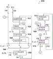
为了让AES编码器的面积小于两套AES编码电路的面积,从一个方面来说,参考图5,本发明实施例提出在AES编码器500中除了设置用于实现如上所示算法的AES编码电路510之外,还设置面积较一套完整的AES编码电路510更小的错误侦测电路530来完成加密过程是否发生错误的侦测。在每个体的加密过程中,错误侦测电路530使用比16个体及其所属的回合密钥更少的信息来判断整个加密过程中是否发生错误。如果判定没有任何错误,则错误侦测电路530可输出加密成功信息。如果判定发生错误,则错误侦测电路530输出加密失败的信息,用于通知处理单元中运行的固件,需要执行错误管理程序。In order to make the area of the AES encoder smaller than the area of the two sets of AES encoding circuits, from one aspect, referring to FIG. In addition to 510, an
冗余数据产生电路550可在16个体附加上用于让错误侦测电路530判断加密过程中是否发生错误的冗余数据,而冗余数据是一种根据16个体中的值或者中间加密结果和AES加密算法的预测结果。参考图6,在一些实施例中,冗余数据产生电路(Redundant-dataGeneration Circuitry)550可预测一个体内奇偶校验比特(In-state Parity Bit),并且将体内奇偶校验比特(当作第8个比特)附加在体(第0~7个比特)之后。需要注意的是,所属技术领域人员不应依据上述的附加操作解读为8比特的体和1比特的体内奇偶校验比特实际存储于9比特的连续空间,不同但等同的数据结构都是允许的。例如,冗余数据产生电路550可预测体S0的体内奇偶校验比特P0,预测体S1的体内奇偶校验比特P1,依此类推。体和相应体内奇偶校验比特之间的匹配可使用以下示例公式表示:Redundant data generating circuit 550 can add redundant data for allowing

Pi代表第i个体的体内奇偶校验比特的值,Si,j代表第i个体中的第j个比特的值,i为从0到15的正整数。当公式的两边相等时,代表第i个体和第i个体内奇偶校验比特是匹配的。否则,代表两者间不匹配。冗余数据产生电路550可预测相应于每列的体的值及其体内奇偶校验比特的一个跨体奇偶校验9比特(Across-state Parity 9-bit)。例如,冗余数据产生电路550可预测相应于体S0及其体内奇偶校验比特P0、体S1及其体内奇偶校验比特P1、体S2及其体内奇偶校验比特P2和体S3及其体内奇偶校验比特P3的跨体奇偶校验9比特Q0,依此类推。每个列的多个体及其体内奇偶校验比特和相应跨体奇偶校验9比特之间的匹配可使用以下示例公式表示:Pi represents the value of the internal parity bit of the i-th individual, Si,j represents the value of the j-th bit in the i-th individual, and i is a positive integer from 0 to 15. When both sides of the formula are equal, it means that the i-th individual and the parity bits in the i-th individual match. Otherwise, there is a mismatch between the two. The redundant data generation circuit 550 may predict an Across-state Parity 9-bit corresponding to the bank value of each column and its bank parity bits. For example,the redundant datageneratingcircuit550 may predictthe corresponding And body S3 and its body parity bit P3


Q0,j代表第0个跨体奇偶校验9比特的第j个比特的值,Q1,j代表第1个跨体奇偶校验9比特的第j个比特的值,Q2,j代表第2个跨体奇偶校验9比特的第j个比特的值,Q3,j代表第3个跨体奇偶校验9比特的第j个比特的值,Si,j代表第i个体中的第j个比特的值,j为从0至8的任意整数。当第i个跨体奇偶校验9比特中的每个比特等于第i列中的相应比特的加总(或者互斥或运算的结果)时,代表第i列的体及体内奇偶校验比特和第i个跨体奇偶校验9比特之间是匹配的。否则,代表两者间不匹配。Q0, j represents the value of the jth bit of the 0th spanning parity check 9 bits, Q1, j represents the value of the jth bit of the 1st spanning parity check 9 bits, Q2, j Represents the value of the jth bit of the second spanning parity check 9 bits, Q3,j represents the value of the jth bit of the third spanning body parity check 9 bits, Si,j represents the ith individual The value of the jth bit in , where j is any integer from 0 to 8. When each bit in the i-th straddle body parity check 9 bits is equal to the sum of the corresponding bits in the i-th column (or the result of a mutually exclusive OR operation), it represents the body and body parity bits in the i-th column It matches with the 9 bits of the i-th spanning parity check. Otherwise, there is a mismatch between the two.
从一个方面来说,AES编码电路510和冗余数据产生电路550是独立且并行运行的,两者之间不会进行数据和信息交换。冗余数据产生电路550使用冗余数据更新算法来产生预测冗余数据,而冗余数据更新算法是从AES加密算法推导出来的,使得AES编码电路510产生的中间加密结果和冗余数据产生电路550预测的冗余数据能够在加密明文过程中的每个特定中间点,在没有发生错误的情况下,都能维持指定的数学关系。From one aspect, the
冗余密钥产生电路(Redundant-key Generation Circuitry)570在每个基础密钥或者回合密钥附加上用于让错误侦测电路530判断密钥产生过程中是否发生错误的冗余数据,而冗余数据是一种根据基础密钥或者回合密钥中的值和AES密钥调度算法的预测结果。参考图7,以256比特基础密钥为例,冗余密钥产生电路570可先将基础密钥依序切分为32个字节(每个字节可称为小钥,Subkey),并组织为8列4行的矩阵。冗余密钥产生电路570可预测一个小钥内奇偶校验比特(In-subkey Parity Bit),并且将小钥内奇偶校验比特(当作第8个比特)附加在小钥(第0~7个比特)之后。需要注意的是,所属技术领域人员不能够依据上述的附加操作解读为8比特的小钥和1比特的小钥内奇偶校验比特实际存储于9比特的连续空间,不同但等同的数据结构都是允许的。例如,冗余密钥产生电路570可预测小钥K0的小钥内奇偶校验比特R0,预测小钥S1的小钥内奇偶校验比特R1,依此类推。小钥和小钥内奇偶校验比特之间的匹配可使用以下示例公式表示:Redundant-key Generation Circuitry (Redundant-key Generation Circuitry) 570 adds redundant data for allowing

Ri代表第i个小钥的小钥内奇偶校验比特的值,Ki,j代表第i个小钥中的第j个比特的值,i为从0到15的正整数。当公式的两边相等时,代表第i个小钥和第i个小钥内奇偶校验比特是匹配的。否则,代表两者间不匹配。冗余密钥产生电路570可预测相应于每列的小钥的值及其小钥内奇偶校验比特的一个跨小钥奇偶校验9比特(Across-subkey Parity 9-bit)。例如,冗余密钥产生电路570可预测相应于小钥k0及其小钥内奇偶校验比特R0、小钥k1及其体内奇偶校验比特R1、小钥k2及其小钥内奇偶校验比特R2和小钥k3及其小钥内奇偶校验比特R3的跨小钥奇偶校验9比特V0,依此类推。每个列的多个小钥及其小钥内奇偶校验比特和相应跨小钥奇偶校验9比特之间的匹配可使用以下示例公式表示:Ri represents the value of the parity bit in the i-th small key, Ki,j represents the value of the j-th bit in the i-th small key, and i is a positive integer from 0 to 15. When both sides of the formula are equal, it means that the i-th small key matches the parity bits in the i-th small key. Otherwise, there is a mismatch between the two. The redundant


V0,j代表第0个跨小钥奇偶校验9比特的第j个比特的值,V1,j代表第1个跨小钥奇偶校验9比特的第j个比特的值,V2,j代表第2个跨小钥奇偶校验9比特的第j个比特的值,V3,j代表第3个跨小钥奇偶校验9比特的第j个比特的值,V4,j代表第4个跨小钥奇偶校验9比特的第j个比特的值,V5,j代表第5个跨小钥奇偶校验9比特的第j个比特的值,V6,j代表第6个跨小钥奇偶校验9比特的第j个比特的值,V7,j代表第7个跨小钥奇偶校验9比特的第j个比特的值,ki,j代表第i个小钥中的第j个比特的值,j为从0至8的任意整数。当第i个跨小钥奇偶校验9比特中的每个比特等于第i列中的相应比特的加总(或者互斥或运算的结果)时,代表第i列的小钥及小钥内奇偶校验比特和第i个跨小钥奇偶校验9比特之间是匹配的。否则,代表两者间不匹配。V0,j represents the value of the jth bit of the 0th 9-bit cross-key parity check, V1,j represents the value of the j-th bit of the first 9-bit cross-key parity check, V2 ,j represents the value of the jth bit of the second 9-bit cross-key parity check, V3,j represents the value of the j-th bit of the third 9-bit cross-key parity check, V4,j Represents the value of the jth bit of the fourth 9-bit cross-key parity check, V5,j represents the value of the j-th bit of the fifth 9-bit cross-key parity check, V6,j represents the value of the j-th bit The value of the j-th bit of the 9-bit cross-key parity check, V7,j represents the value of the j-th bit of the 7th cross-key parity check 9-bit value, ki,j represents the i-th The value of the jth bit in the key, where j is any integer from 0 to 8. When each bit in the 9 bits of parity check across the i-th small key is equal to the sum of the corresponding bits in the i-th column (or the result of a mutually exclusive OR operation), it represents the small key in the i-th column and the key in the i-th column There is a match between the parity check bits and the i-th cross-key parity check 9 bits. Otherwise, there is a mismatch between the two.
从一个方面来说,AES编码电路510和冗余密钥产生电路570是独立且并行运行的,两者之间不会进行数据和信息交换。冗余密钥产生电路570使用冗余密钥更新算法来产生预测冗余数据,而冗余密钥更新算法是从AES加密算法中的AES密钥调度推导出来的,使得AES编码电路510产生的回合密钥和冗余密钥产生电路570预测的冗余数据能够在产生回合密钥过程中的每个特定中间点,在没有发生错误的情况下,都能维持指定的数学关系。From one aspect, the
虽然图5将AES编码电路510、错误侦测电路530、冗余数据产生电路550和冗余密钥产生电路570以不同方块表示,但这只是为了让读者容易理解,所属技术领域人员可在实际实现时,将AES编码电路510、错误侦测电路530、冗余数据产生电路550和冗余密钥产生电路570以适当的方式整合在一起,本发明并不因此局限。Although FIG. 5 shows the
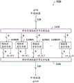
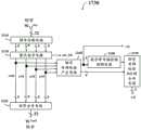
从另一个方面来说,参考图8,本发明实施例提出在AES编码器137中设置AES数据处理电路(AES Data Processing Circuitry)810和AES密钥调度电路(AES Key ScheduleCircuitry)830。AES密钥调度电路830包含密钥产生电路833,用于完成如图3所示的扩展密钥步骤S350。控制器870发出控制信号给AES密钥调度电路830,用于驱动AES密钥调度电路830根据基础密钥K0或者之前的回合密钥Ki产生新的回合密钥,并且输出指定回合的回合密钥Ki及其相应的冗余数据(例如,小钥内奇偶校验比特R和跨小钥奇偶校验9比特V)给AES数据处理电路810。AES密钥调度电路830包含密钥错误检查电路835,设置以计算出相应于每个回合密钥的冗余数据;并且在扩展密钥过程中的指定中间点发现任何回合密钥和相应冗余数据不匹配时,发出错误信号ERR_KEY=1。回合密钥可切分为16个小钥且组织为4×4字节数组,每个小钥为1字节;冗余数据包含相应于每个小钥的小钥内奇偶校验比特,和相应于每个列的跨小钥奇偶校验9比特。密钥错误检查电路835在扩展密钥过程中的指定中间点发现任何小钥不匹配于相应小钥内奇偶校验比特时,或者发现相应于任何列的小钥加上4个相应小钥内奇偶校验比特,不匹配于相应跨小钥奇偶校验9比特时,发出错误信号ERR_KEY=1。From another aspect, referring to FIG. 8 , the embodiment of the present invention proposes setting an AES data processing circuit (AES Data Processing Circuitry) 810 and an AES key scheduling circuit (AES Key Schedule Circuitry) 830 in the
AES数据处理电路810包含编码电路813,设置以实现如图3所示的AES算法中的替代字节步骤S310、位移行步骤S320、混合列步骤S330和加上回合密钥步骤S340。AES算法包含多个回合,并且在每个回合中用于使用回合密钥对明文或者中间加密结果进行编码。控制器870发出控制信号给AES数据处理电路810,用于驱动AES数据处理电路810来安排上述步骤的执行顺序,以符合AES算法的回合设置。AES数据处理电路810包含编码错误检查电路815,设置以计算出相应于明文或者中间加密结果的冗余数据;在加密过程中的指定中间点发现中间加密结果和冗余数据之间不匹配时,发出编码错误信号ERR_ENC=1。明文可切分为16个体且组织为4×4数组,每个体为1字节,第二冗余数据包含相应于每个体的体内奇偶校验比特,和相应于明文中的每个列的跨体奇偶校验9比特。编码错误检查电路815在加密过程中的指定时间点发现任何所述体的中间加密结果不匹配于相应体内奇偶校验比特时,或者发现相应于明文中的任何列的中间加密结果加上4个相应体内奇偶校验比特,不匹配于相应跨体奇偶校验9比特时,发出编码错误信号ERR_ENC=1。The AES
或门850耦接编码错误检查电路815和密钥错误检查电路835的输出端。当编码错误检查电路815输出编码错误信号ERR_ENC=1和/或密钥错误检查电路835输出密钥错误信号ERR_KEY=1时,或门850输出AES错误信号ERR_AES=1给处理单元134。The OR
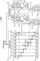
参考图9所示的AES数据处理电路810的框图。数据寄存器912用于存储在AES加密过程中产生的16字节(也就是128比特)的中间或者最终结果,而奇偶校验码寄存器(ParityRegisters)914用于存储在AES加密过程中产生的相应于16字节的中间或者最终结果的体内奇偶校验比特和跨体奇偶校验9比特。位移行电路(Shift-row Circuitry)930用于执行如如图3所示的位移行的步骤S320,并且其结构为所属技术领域人员所公知,为求简明不再赘述。混合列电路(Mix-column Circuitry)940用于执行如如图3所示的混合列的步骤S330,并且其结构为所属技术领域人员所公知,为求简明不再赘述。加上回合密钥电路(Add-round-key Circuitry)950用于执行如如图3所示的加上回合密钥的步骤S340,并且其结构为所属技术领域人员所公知,为求简明不再赘述。Refer to the block diagram of the AES
控制器870可在每个回合发出选择信号R_sel给复用器980和奇偶校验预测电路(Parity Prediction Circuitry)970,用于控制流经指定电路的数据流。复用器980包含三个输入端I0、I1及I2和一个输出端O。输入端I0耦接AES编码器137的输入引脚以接收16字节的明文,输入端I1耦接混合列电路940的输出以接收16字节的运算结果,输入端I2耦接位移行电路930的输出以接收16字节的运算结果,输出端O耦接加上回合密钥电路950的输入。详细来说,在初始回合,控制器870可使用控制信号R_sel控制复用器980将输入端I0连接上输出端O,使得从AES编码器137的输入引脚接收到的16字节的明文S能够馈入加上回合密钥电路950。在中间回合(例如使用256比特密钥的第1至第13回合),控制器870可使用控制信号R_sel控制复用器980将输入端I1连接上输出端O,使得混合列电路940的输出能够馈入加上回合密钥电路950。在最终回合(例如使用256比特密钥的第14回合),控制器870可使用控制信号R_sel控制复用器980将输入端I2连接上输出端O,使得位移行电路930的输出能够馈入加上回合密钥电路950。此外,在初始回合,控制器870可使用控制信号R_sel控制奇偶校验预测电路970,让从AES编码器137的输入引脚接收到的16字节的明文S能够馈入奇偶校验预测电路970,用于产生相应于明文的体内奇偶校验比特P和跨体奇偶校验9比特Q。在中间和最终回合,控制器870可使用控制信号R_sel控制奇偶校验预测电路970,让增强型替代字节电路920的输出能够馈入奇偶校验预测电路970,用于产生相应于中间加密结果的体内奇偶校验比特P和跨体奇偶校验9比特Q。The
参考图10所示的奇偶校验预测电路970的框图。奇偶校验预测电路970包含体内奇偶校验比特预测电路(In-state Parity-bit Prediction Circuitry)1010和跨体奇偶校验9比特预测电路(Across-state Parity-9-bit Prediction Circuitry)1030。体内奇偶校验比特预测电路1010依据控制信号R_sel选择输入明文S(相应于初始回合)或者中间加密结果S’(相应于中间或者最终回合),并且根据明文S/中间加密结果S’和小钥内奇偶校验比特R产生体内奇偶校验比特P。跨体奇偶校验9比特预测电路1030依据控制信号R_sel选择输入明文S(相应于初始回合)或者中间加密结果S’(相应于中间或者最终回合),并且根据明文S/中间加密结果S’和跨小钥奇偶校验9比特V产生跨体奇偶校验9比特Q。Refer to the block diagram of the
参考图11所示的体内奇偶校验比特预测电路1010的框图。控制器870可在每个回合发出选择信号R_sel给复用器1140和体内奇偶校验比特产生电路1110,用于控制流经指定电路的数据流。复用器1140包含三个输入端I0、I1及I2和一个输出端O。输入端I0耦接体内奇偶校验比特产生电路1110的输出以接收相应于明文的16比特的体内奇偶校验码,输入端I1耦接混合列预测电路1130的输出以接收16比特的运算结果,输入端I2耦接位移行预测电路1120的输出以接收16比特的运算结果,输出端O耦接加上回合密钥预测电路950的输入。详细来说,在初始回合,控制器870可使用控制信号R_sel驱动体内奇偶校验比特产生电路1110从AES编码器137的输入引脚接收16字节的明文,并且控制复用器1140将输入端I0连接上输出端O,使得从体内奇偶校验比特产生电路1110的输出所接收到的相应于明文S的16比特的体内奇偶校验码能够馈入加上回合密钥预测电路1150。在中间回合(例如使用256比特密钥的第1至第13回合),控制器870可使用控制信号R_sel驱动体内奇偶校验比特产生电路1110从数据寄存器912获取16字节的中间加密结果S’,并且控制复用器1140将输入端I1连接上输出端O,使得从混合列预测电路1130的输出所接收到的相应于中间加密结果S’的16比特的体内奇偶校验码能够馈入加上回合密钥预测电路1150。在最终回合(例如使用256比特密钥的第14回合),控制器870可使用控制信号R_sel驱动体内奇偶校验比特产生电路1110从数据寄存器912获取16字节的中间加密结果S’,并且控制复用器1140将输入端I2连接上输出端O,使得从位移行预测电路1120的输出所接收到的相应于中间加密结果S’的16比特的体内奇偶校验码能够馈入加上回合密钥预测电路1150。Refer to the block diagram of the intra-body parity
参考图12所示的体内奇偶校验比特产生电路1110的框图。控制器870可在每个回合发出选择信号R_sel给复用器1210,用于控制流经指定电路的数据流。复用器1210包含两个输入端I0及I1和一个输出端O。详细来说,在初始回合,控制器870可使用控制信号R_sel控制复用器1210将输入端I0连接上输出端O,使得从AES编码器137的输入引脚所接收到的16字节的明文S能够馈入加上体内互斥或门1230。在中间和最终回合(例如使用256比特密钥的第1至第14回合),控制器870可使用控制信号R_sel控制复用器1210将输入端I1连接上输出端O,使得从数据寄存器912获取16字节的中间加密结果S’能够馈入体内互斥或门1230。体内互斥或门1230包含多个互斥或门,安排以依据接收到的16字节的明文S或者中间加密结果S’,产生如图6所示的体内奇偶校验比特P0至P15。Refer to the block diagram of the internal parity
参考回图11,明文S或中间加密结果S’组织为4×4个体的数组。位移行电路1160用于将下面三行的每一者向左循环位移指定步数。举例来说,明文S表示如下:Referring back to Fig. 11, the plaintext S or the intermediate encryption result S' is organized as an array of 4×4 entities. The line shift circuit 1160 is used to cyclically shift each of the lower three lines to the left by a specified number of steps. For example, the plaintext S is expressed as follows:

位移行电路1160用于将第一行向左循环位移一个体,将第二行向左循环位移两个体,以及将第三行向左循环位移三个体。位移结果如下所示:The row shift circuit 1160 is used to cyclically shift the first row to the left by one bank, the second row to the left by two banks, and the third row to the left by three banks. The displacement results are as follows:

相应于明文S或中间加密结果S’的体内奇偶校验字节织为4×4个比特的数组。位移行预测电路1120用于将下面三行的每一者向左循环位移指定步数。举例来说,相应于明文S的体内奇偶校验比特表示如下:The body parity bytes corresponding to the plaintext S or the intermediate encryption result S' are woven into an array of 4x4 bits. The row-

位移行预测电路1120用于将第一行向左循环位移一个比特,将第二行向左循环位移两个比特,以及将第三行向左循环位移三个比特。位移结果如下所示:The row-

混合列预测电路1130耦接位移行预测电路1120和位移行电路1160的输出,使用所属技术领域人员所习知的16个公式,每个公式加总位移后的明文S或中间加密结果S’的4×4字节数组以及位移后的体内奇偶校验比特的4×4比特数组中指定部分的值,产生混合后的体内奇偶校验比特的矩阵中的指定的值。The hybrid
加上回合密钥预测电路1150使用以下公式计算体内奇偶校验比特的加密后结果:Plus the round
P(out)i=P(in)i+RiP(out)i = P(in)i + Ri
P(out)i代表输出的第i个体的体内奇偶校验比特,P(in)i代表输入的第i个体的体内奇偶校验比特,Ri代表第i个小钥内奇偶校验比特,i为从0至15的任意整数。需要注意的是,此时P(in)i和P(out)i所对应到的矩阵中的位置指的是混合列预测电路1130所输出矩阵中的位置,不是对应到体内奇偶校验比特产生电路1110所输出矩阵中的位置。P(out)i represents the internal parity bits of the i-th individual output, P(in)i represents the internal parity bits of the i-th individual input, and Ri represents the internal parity bits of the i-th small key, i is any integer from 0 to 15. It should be noted that at this time, the positions in the matrix corresponding to P(in)i and P(out)i refer to the positions in the matrix output by the hybrid
参考图13所示的跨体奇偶校验9比特预测电路1030的框图。控制器870可在每个回合发出选择信号R_sel给跨体奇偶校验字节产生电路1310,用于控制跨体奇偶校验字节产生电路1310输入的数据流。详细来说,在初始回合,控制器870可使用控制信号R_sel驱动跨体奇偶校验字节产生电路1310从AES编码器137的输入引脚接收16字节的明文,使得跨体奇偶校验字节产生电路1310依据明文S的16字节产生跨体奇偶校验字节。在中间回合(例如使用256比特密钥的第1至第13回合)或者最终回合(例如使用256比特密钥的第14回合),控制器870可使用控制信号R_sel驱动跨体奇偶校验字节产生电路1310从数据寄存器912获取16字节的中间加密结果S’,使得跨体奇偶校验字节产生电路1310依据中间加密结果S’的16字节产生跨体奇偶校验字节。Refer to the block diagram of the cross-body parity 9-
跨体奇偶校验字节产生电路1310包含多个互斥或门,在初始回合安排以依据接收到的16字节的明文S,完成如图6所示的跨体奇偶校验字节(不包含相应于体内奇偶校验比特的第8比特)Q0,0..7至Q3,0..7。在中间回合或者最终回合安排以依据接收到的16字节的中间加密结果S’,并且使用以下公式计算跨体奇偶校验字节(不包含相应于体内奇偶校验比特的第8比特)Q0,0..7至Q3,0..7:The cross-body parity
Q0,j=S′0,j+S′5,j+S′10,j+S′15,j,for j=0~7Q0, j = S'0, j + S'5, j + S'10, j + S'15, j , for j=0~7
Q1,j=S′4,j+S′9,j+S′14,j+S′3,j,for k=0~7Q1, j = S'4, j + S'9, j + S'14, j + S'3, j , for k=0~7
Q2,j=S′8,j+S′13,j+S′2,j+S′7,j,for j=0~7Q2, j = S'8, j + S'13, j + S'2, j + S'7, j , for j=0~7
Q3,j=S′12,j+S′1,j+S′6,j+S′11,j,for j=0~7Q3, j = S'12, j + S'1, j + S'6, j + S'11, j , for j=0~7
Q0,j到Q3,j分别代表第0个到第3个跨体奇偶校验字节的第j个比特的值,S’0,j到S’15,j分别代表相应于第0个到第15个中间加密结果中的第j个比特的值。Q0, j to Q3, j respectively represent the value of the jth bit of the 0th to the 3rd spanning parity byte, and S'0, j to S'15, j represent the values corresponding to the 0th bit The value of the j-th bit in the 15th to 15th intermediate encrypted results.
跨小钥奇偶校验字节分割电路(Across-subkey Parity-byte Split Circuitry)1330移除每个跨小钥奇偶校验9比特的第8个比特,成为跨小钥奇偶校验字节,并且将跨小钥奇偶校验字节馈入跨体奇偶校验字节预测电路1350。Across-subkey Parity-byte Split Circuitry (Across-subkey Parity-byte Split Circuitry) 1330 removes the 8th bit of each 9-bit cross-subkey parity to become a cross-subkey parity byte, and The cross-key parity bytes are fed into the cross-body parity
跨体奇偶校验字节预测电路1350使用以下公式计算每个跨体奇偶校验字节的预测结果:The span parity


Q(out)0,j代表输出的第0个跨体奇偶校验字节的第j个比特的值,Q(out)1,j代表输出的第1个跨体奇偶校验字节的第j个比特的值,Q(out)2,j代表输出的第2个跨体奇偶校验字节的第j个比特的值,Q(out)3,j代表输出的第3个跨体奇偶校验字节的第j个比特的值,Q(in)i,j代表输入的第i个跨体奇偶校验字节的第j个比特的值,Vi,j代表第i个跨小钥奇偶校验字节中的第.j个比特的值。Q(out)0, j represents the value of the jth bit of the 0th straddle parity byte output, Q(out)1, j represents the value of the 1st straddle parity byte output The value of j bits, Q(out)2, j represents the value of the jth bit of the second spanning parity check byte output, Q(out)3, j represents the third spanning parity output The value of the jth bit of the check byte, Q(in)i, j represents the value of the jth bit of the input ith span parity byte, Vi, j represents the value of the ith span small The value of the jth bit in the key parity byte.
跨体奇偶校验1比特预测电路1370使用以下公式计算每个跨体奇偶校验9比特的第8个比特的预测结果:The


Q0,8代表第0个列的跨体奇偶校验9比特的第8个比特的值,Q1,8代表第1个列的跨体奇偶校验9比特的第8个比特的值,Q2,8代表第2个列的跨体奇偶校验9比特的第8个比特的值,Q3,8代表第3个列的跨体奇偶校验9比特的第8个比特的值,Pi,8代表相应于第i个体的体内奇偶校验比特(也就是第8个比特)的值。Q0,8 represents the value of the 8th bit of the 9-bit cross-body parity check of the 0th column, Q1,8 represents the value of the 8th bit of the 9-bit cross-body parity check of the 1st column, Q2,8 represents the value of the 8th bit of the 9-bit cross-body parity check of the second column, and Q3,8 represents the value of the 8th bit of the 9-bit cross-body parity check of the third column, Pi,8 represents the value of the internal parity bit (that is, the 8th bit) corresponding to the i-th individual.
跨体奇偶校验9比特合并电路(Across-state Parity-9-bit ConcatenationCircuitry)1390将每个从跨体奇偶校验字节预测电路1350输出的跨体奇偶校验字节,附加上从跨体奇偶校验1比特预测电路1370输出的相应第8个比特,成为完整的跨体奇偶校验9比特。The Across-state Parity-9-bit Concatenation Circuitry (Across-state Parity-9-bit Concatenation Circuitry) 1390 adds each Across-state Parity byte output from the Across-state Parity
参考回图9,奇偶校验检查电路(Parity Check Circuitry)960检查上一回合的执行结果是否发生错误。奇偶校验检查电路960从数据寄存器912获取中间加密结果S’,以及从奇偶校验码寄存器914获取相应于中间加密结果S’的体内奇偶校验比特P和跨体奇偶校验9比特Q。奇偶校验检查电路960判断中间的加密结果S’和体内奇偶校验比特P之间是否匹配,如果不匹配,则发出线性错误信号err_L=1给处理单元134,使得处理单元134执行任何因应AES加密错误的管理程序。奇偶校验检查电路960还判断中间的加密结果S’、中间的体内奇偶校验比特P和跨体奇偶校验9比特Q之间是否匹配,如果不匹配,则发出线性错误信号err_L=1给处理单元134。Referring back to FIG. 9 , a parity check circuit (Parity Check Circuitry) 960 checks whether an error occurs in the execution result of the previous round. The
增强型替代字节电路(Enhanced Substitute-byte Circuitry)920除了完成算法中的替代字节步骤S310之外,也要检查此步骤的执行结果是否正确。参考图14所示的增强型替代字节电路920的框图。跨体奇偶校验字节分割电路1410从数据寄存器912获取128比特的中间结果S’,切分为16个字节,并且将这16个字节分别馈入增强型查表电路1430#0至1430#15。增强型查表电路1430#0至1430#15中的每一个完成替代字节步骤S310,并且判断此操作是否正确。如果增强型查表电路1430#0至1430#15中的任何一个发现此操作错误,则输出非线性错误信号err_nl_i=1,i为0到15的正整数。只要任何一个增强型查表电路输出非线性错误信号err_nl_i,则增强型替代字节电路920输出非线性错误信号err_nL=1给处理单元134,使得处理单元134执行任何因应AES加密错误的管理程序。跨体奇偶校验字节合并电路1450搜集增强型查表电路1430#0至1430#15的查表结果,并且将转换后的128比特输出到位移行电路930。The Enhanced Substitute-byte Circuit (Enhanced Substitute-byte Circuit) 920, in addition to completing the substitute-byte step S310 in the algorithm, also checks whether the execution result of this step is correct. Refer to the block diagram of the enhanced
参考图15所示的增强型查表电路1430#i的框图,i为0到15的正整数。搜索电路1510依据如上所述的查找表将输入的1个字节S’(in)转换出1个字节S’(out)。替代校验电路(Substitution Check Circuitry)1530从搜索电路1510接收转换后的1个字节S’(out),并且使用相应于查找表的公式判断S’(in)转换到S’(out)的过程中是否发生错误。如果发现错误,则替代校验电路1530输出非线性错误信号err_nl_i=1。Referring to the block diagram of the enhanced look-up
参考图16所示的替代校验电路1530的框图。计算电路1610从搜索电路1510获取转换后的字节S’(out)i,计算Affine(S’(out))-1,Affine()-1代表Affine转换的反函数,并且将计算结果输出到乘法器1630和比较器1650。乘法器1630将S’(in)乘上Affine(S’(out))-1以产生S’(mul)。比较器1650实施以下逻辑表达式来产生判断结果:Refer to the block diagram of the
err_nl_i=0,if(S’(mul)==1)&&(S’(in)i!=0)&&(Affine(S’(out))-1!=0)err_nl_i=0, if(S'(mul) ==1)&&(S'(in)i !=0)&&(Affine(S'(out) )-1 !=0)
err_nl_i=0,if(S’(mul)==0)&&(S’(in)i==0)&&(Affine(S’(out))-1==0)err_nl_i=0, if(S'(mul) ==0)&&(S'(in)i ==0)&&(Affine(S'(out) )-1 ==0)
err_nl_i=1,otherwiseerr_nl_i=1, otherwise
当err_nl_i等于1时,代表发生非线性错误信号。When err_nl_i is equal to 1, it represents a non-linear error signal.
数据寄存器912、搜索电路1510、位移行电路930、混合列电路940、复用器980和加上回合密钥电路950可视为AES编码电路。奇偶校验码寄存器914、替代校验电路1530、奇偶校验检查电路960和奇偶校验预测电路970可视为错误检查电路。The data register 912, the
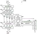
参考图17所示的AES密钥调度电路830的框图。密钥分割电路1750将256比特的基础密钥K0切分为2个密钥K#0和K#1,每个钥字的长度为128比特,相同于一个体的长度。密钥奇偶校验码产生电路(Key Parity Generation Circuitry)1742包含多个互斥或门,安排以依据接收到的密钥K#0,产生如图7所示的小钥内奇偶校验比特R0至R15(可统称为R#0),以及跨小钥奇偶校验9比特V0至V3(可统称为V#0),并且将小钥内奇偶校验比特R#0和跨小钥奇偶校验9比特V#0存储到寄存器1752。密钥奇偶校验码产生电路1744包含多个互斥或门,安排以依据接收到的密钥K#1,产生如图7所示的小钥内奇偶校验比特R16至R31(可统称为R#1),以及跨小钥奇偶校验9比特V4至V7(可统称为V#1),并且将小钥内奇偶校验比特R#1和跨小钥奇偶校验9比特V#1存储到寄存器1754。寄存器1752和1754又可称为目前周期奇偶校验寄存器(Current Cycle Parity Registers)。Refer to the block diagram of the AES
密钥奇偶校验检查电路(Key Parity Check Circuitry)1762和1764分别检查密钥K#0和K#1的产生是否发生错误。密钥奇偶校验检查电路1762从密钥分割电路1750获取密钥K#0,以及从寄存器1752获取相应于密钥K#0的小钥内奇偶校验比特R#0和跨小钥奇偶校验9比特V#0。密钥奇偶校验检查电路1762判断密钥K#0和小钥内奇偶校验比特R#0之间是否匹配,如果不匹配,则发出密钥错误信号err_kc=1。密钥奇偶校验检查电路1762还判断密钥K#0、小钥内奇偶校验比特R#0和跨小钥奇偶校验9比特V#0之间是否匹配,如果不匹配,则发出密钥错误信号err_kc=1。密钥奇偶校验检查电路1764从密钥分割电路1750获取密钥K#1,以及从寄存器1754获取相应于密钥K#1的小钥内奇偶校验比特R#1和跨小钥奇偶校验9比特V#1。密钥奇偶校验检查电路1764判断密钥K#1和小钥内奇偶校验比特R#1之间是否匹配,如果不匹配,则发出密钥错误信号err_kd=1。密钥奇偶校验检查电路1764还判断密钥K#1、小钥内奇偶校验比特R#1和跨小钥奇偶校验9比特V#1之间是否匹配,如果不匹配,则发出密钥错误信号err_kd=1。密钥错误信号err_kc=1或者err_kd=1可触发处理单元134执行任何因应AES密钥错误的管理程序。Key parity check circuits (Key Parity Check Circuitry) 1762 and 1764 respectively check whether an error occurs in the generation of
密钥分割电路1710将256比特的基础密钥K0切分为8个钥字(Word)W0,0至W0,3和W1,0至W1,3,每个钥字的长度为4个字节,并且将8个钥字存储在寄存器1712。钥字处理电路1720根据最后一个钥字W1,3产生一个钥字的中间运算结果,此运算结果被用于和第一个钥字W0,0进行逐比特逻辑互斥或运算(Bitwise Logical XOR Operation),以产生密钥K#2的第一个钥字W2,0。除了产生中间运算结果以外,钥字处理电路1720还可以检查中间运算结果的产生过程是否发生错误。如果是,则钥字处理电路1720输出密钥错误信号err_ka=1。密钥错误信号err_ka=1可触发处理单元134执行任何因应AES密钥错误的管理程序。The
参考图18所示的钥字处理电路1720的框图。钥字分割电路1810从寄存器1712读取最后一个钥字W1,3,并且切分为4个小钥,每个小钥为1字节。旋转钥字电路(Rotate-WordCircuitry)1820将这4个小钥向左循环位移1个小钥。替代钥字电路(Substitute-WordCircuitry)1830根据查找表(又可称为Rijndael S-box)将每个位移后小钥的值替换为另一个值,其中的查找表使用以下公式建立:Refer to the block diagram of the key
SBi=Affine((i)-1),for i=0~127SBi =Affine((i)-1 ), for i=0~127
SBi代表i的输出结果,Affine()代表Affine转换函数,i为从0到127的正整数。替代钥字电路1830除了完成每个输入字节的值的转换之外,也要检查转换的执行结果是否正确。SBi represents the output result of i, Affine() represents the Affine conversion function, and i is a positive integer from 0 to 127. In addition to completing the conversion of the value of each input byte, the substitution
参考图19所示的替代钥字电路1830的框图。增强型查表电路1930#0至1930#3中的每一个完成相应字节的值的替换操作,并且判断此操作是否正确。如果增强型查表电路1930#0至1930#3中的任何一个发现此操作错误,则输出查表错误信号err_w_i=1,i为0到3的正整数。只要任何一个增强型查表电路输出查表错误信号err_w_i,则替代钥字电路1830输出密钥错误信号err_ka=1给处理单元134,使得处理单元134执行任何因应AES加密错误的管理程序。由于增强型查表电路1930#0至1930#3中的任一个的电路结构、功能和操作细节类似于增强型查表电路1430#i,所以读者可参考图15和图16的描述,为求简明不再赘述。Refer to the block diagram of the substitute
参考回图18,舍去常数电路(Round-Constant Circuitry)1840将钥字w#0(in)和常数C执行逐比特互斥或(XOR)操作。参考图20所示的舍去常数电路1840的示意图。XOR闸2010设置将钥字w#0(in)的每个比特和常数C的相应比特执行逻辑互斥或操作。Referring back to FIG. 18 , the round-constant circuit (Round-Constant Circuitry) 1840 performs a bit-by-bit exclusive OR (XOR) operation on the key
钥字合并电路(Word Concatenation Circuitry)1850从舍去常数电路1840获取4个小钥w#0至w#3,合并小钥w#0至w#3为完整的钥字W(out),并且输出钥字W(out)至互斥或门1725。The word concatenation circuit (Word Concatenation Circuitry) 1850 obtains 4 small
钥字奇偶校验产生电路(Word Parity Generation Circuitry)1860包含小钥内奇偶校验产生电路和跨小钥奇偶校验产生电路。小钥内奇偶校验产生电路包含多个互斥或门,安排以依据从替代钥字电路1830接收到的小钥w#0至w#3,产生4个小钥内奇偶校验比特rt10至rt13。跨小钥奇偶校验产生电路包含多个互斥或门,安排以依据从替代钥字电路1830接收到的小钥w#0至w#3,产生1个跨小钥奇偶校验字节vt10..7。The key word parity generation circuit (Word Parity Generation Circuitry) 1860 includes a small-key intra-key parity generation circuit and an inter-small-key parity generation circuit. The intra-key parity generating circuit comprises a plurality of mutually exclusive OR gates arranged to generate four intra-key parity bitsrt1 0 according to the
钥字奇偶校验预测电路(Word Parity Prediction Circuitry)1870包含小钥内奇偶校验预测电路和跨小钥奇偶校验预测电路。小钥内奇偶校验预测电路使用以下公式预测小钥内奇偶校验码rt10(out),并且输出到钥字跨奇偶校验预测电路(Word Cross-parityPrediction Circuit)1880和密钥奇偶校验预测电路(Key Parity Prediction Circuit)1772:The key word parity prediction circuit (Word Parity Prediction Circuit) 1870 includes a parity prediction circuit within a small key and a parity prediction circuit across small keys. The parity prediction circuit in the small key uses the following formula to predict the parity code rt10(out) in the small key, and outputs it to the Word Cross-parity Prediction Circuit (Word Cross-parityPrediction Circuit) 1880 and the key parity Prediction circuit (Key Parity Prediction Circuit) 1772:

rt10(out)代表计算后的第0个小钥内奇偶校验码,rt10(in)代表从钥字奇偶校验产生电路1860接收到的第0个小钥内奇偶校验码,Ci代表舍去常数电路1840中使用的常数C中的第i个比特。此外,小钥内奇偶校验预测电路直接输出从钥字奇偶校验产生电路1860接收到的小钥内奇偶校验码rt11至rt13到钥字跨奇偶校验预测电路1880和密钥奇偶校验预测电路1772。跨小钥奇偶校验预测电路使用以下公式预测跨小钥奇偶校验字节,并且输出到钥字奇偶校验9比特合并电路(Word Parity 9-bit Concatenation Circuit)1890:rt10(out) represents the calculated parity code in the 0th small key, rt10(in) represents the parity code in the 0th small key received from the key word
vt10..7(out)=vt10..7(in)+Cvt10..7(out) =vt10..7(in) +C
vt10..7(out)代表输出的跨小钥奇偶校验字节,vt10..7(in)代表从钥字奇偶校验产生电路1860接收到的跨小钥奇偶校验字节,C代表舍去常数电路1840中使用的常数。vt10..7(out) represents the output cross-key parity byte, and vt10..7(in) represents the cross-key parity byte received from the key word
钥字跨奇偶校验预测电路1880使用以下公式计算跨小钥奇偶校验9比特vt的最后一个比特:Key word cross

vt18代表跨小钥奇偶校验9比特vt的最后一个比特,rt1i代表第i个小钥内奇偶校验比特。vt18 represents the last bit of the 9-bit parity across small keys vt, and rt1i represents the parity bits within the ith small key.
钥字奇偶校验9比特合并电路1890将钥字奇偶校验预测电路1870的计算结果vt10..7合并上钥字跨奇偶校验预测电路1880的计算结果vt18,成为跨钥字奇偶校验9比特vt10..8,并且输出到密钥奇偶校验电路1772。The key word parity 9-
参考回图17,钥字处理电路1730根据互斥或门1727的运算结果(也就是钥字W2,3)产生一个钥字的中间运算结果,此运算结果被用于和钥字W1,0进行逐比特逻辑互斥或运算,以产生密钥K#3的第一个钥字W3,0。除了产生中间运算结果以外,钥字处理电路1730还可以检查中间运算结果的产生过程是否发生错误。如果是,则钥字处理电路1730输出密钥错误信号err_kb=1。密钥错误信号err_kb=1可触发处理单元134执行任何因应AES密钥错误的管理程序。Referring back to FIG. 17 , the key
参考图21所示的钥字处理电路1730的框图。钥字分割电路2110从互斥或门1727读取运算结果(也就是钥字W2,3),并且切分为4个字节。替代钥字电路2130根据查找表将每个字节的值替换为另一个值,其中的查找表使用以下公式建立:Refer to the block diagram of the key
SBi=Affine((i)-1),for i=0~127SBi =Affine((i)-1 ), for i=0~127
SBi代表i的输出结果,Affine()代表Affine转换函数,i为从0到127的正整数。替代钥字电路2130除了完成每个输入字节的值的转换之外,也要检查转换的执行结果是否正确。由于替代钥字电路2130的电路结构、功能和运算结果类似于替代钥字电路1830,所以读者可参考图15、图16和图19的描述,为求简明不再赘述。只要替代钥字电路2130中的任何一个增强型查表电路输出查表错误信号err_w_i,则替代钥字电路2130输出密钥错误信号err_kb=1给处理单元134,使得处理单元134执行任何因应AES加密错误的管理程序。SBi represents the output result of i, Affine() represents the Affine conversion function, and i is a positive integer from 0 to 127. In addition to completing the conversion of the value of each input byte, the substitution
钥字合并电路2150从替代钥字电路2130获取替代后的4个小钥w#0至w#3,合并小钥w#0至w#3为完整的钥字W(out),并且输出钥字W(out)至互斥或门1729。The
钥字奇偶校验产生电路2160包含小钥内奇偶校验产生电路和跨小钥奇偶校验产生电路。小钥内奇偶校验产生电路包含多个互斥或门,安排以依据从替代钥字电路2130接收到的小钥w#0至w#3,产生相应于小钥w#0至w#3的四个小钥内奇偶校验比特rt20至rt23。这四个小钥内奇偶校验比特rt20至rt23输出至钥字跨奇偶校验预测电路2180和密钥奇偶校验预测电路1774。跨小钥奇偶校验产生电路包含多个互斥或门,安排以依据从替代钥字电路2130接收到的小钥w#0至w#3,产生相应于小钥w#0至w#3的一个跨小钥奇偶校验字节vt20..7(也就是缺少跨小钥奇偶校验9比特vt2中的第8个比特)。这个跨小钥奇偶校验字节vt20..7输出至钥字奇偶校验9比特合并电路2190。The key word
钥字跨奇偶校验预测电路2180使用以下公式计算相应于小钥w#0至w#3的跨小钥奇偶校验9比特的最后一个比特:The keyword

vt28代表相应于小钥w#0至w#3的一个跨小钥奇偶校验字节的最后一个比特,rt2i代表相应于小钥w#i的小钥内奇偶校验比特。vt28 represents the last bit of an inter-key parity byte corresponding to
钥字奇偶校验9比特合并电路2190将钥字奇偶校验产生电路2160的计算结果vt20..7合并上钥字跨奇偶校验预测电路2180的计算结果vt28,作为跨钥字奇偶校验9比特vt20..8,并且输出到密钥奇偶校验预测电路1774。The key word parity check 9-
参考回图17,密钥奇偶校验预测电路(Key Parity Prediction Circuitry)1772包含多个加法器,安排以使用以下公式计算出相应于密钥K#2的小钥内奇偶校验比特R#20至R#215:Referring back to FIG. 17, the Key Parity Prediction Circuit (Key Parity Prediction Circuit) 1772 includes a plurality of adders arranged to use the following formula to calculate the parity
R#2i=rt1i+R#0i,for i=0~3
R#2i=R#0i-4+R#0i,for i=4~15
R#2i代表相应于密钥K#2的第i个小钥内奇偶校验比特,rt1i代表从钥字处理电路1720获取的第i个小钥内奇偶校验比特,R#0i代表从寄存器1752读取的相应于密钥K#0的第i个小钥内奇偶校验比特,R#0i-4代表从寄存器1752读取的相应于密钥K#0的第i-4个小钥内奇偶校验比特。密钥奇偶校验预测电路1772另包含多个加法器,安排以使用以下公式计算出相应于密钥K#2的跨小钥奇偶校验9比特V#20至V#23:
V#2i=vt1+V#0i,for i=0
V#2i=V#0i-1+V#0i,for i=1~3
V#2i代表相应于密钥K#2的第i个跨小钥奇偶校验9比特,vt1代表从钥字处理电路1720获取的跨小钥奇偶校验9比特,V#0i代表从寄存器1752读取的相应于密钥K#0的第i个跨小钥奇偶校验9比特,V#0i-1代表从寄存器1752读取的相应于密钥K#0的第i-1个跨小钥奇偶校验9比特。密钥奇偶校验预测电路1772将预测结果R#2、V#2存储到寄存器1782,用于在下一个迭代中让密钥奇偶校验检查电路1762进行检查。
密钥奇偶校验预测电路1774包含多个加法器,安排以使用以下公式计算出相应于密钥K#3的小钥内奇偶校验比特R#30至R#315:The key
R#3i=rt2i+R#1i,for i=0~3
R#3i=R#1i-4+R#1i,for i=4~15
R#3i代表相应于密钥K#3的第i个小钥内奇偶校验比特,rt2i代表从钥字处理电路1730获取的第i个小钥内奇偶校验比特,R#1i代表从寄存器1754读取的相应于密钥K#1的第i个小钥内奇偶校验比特,R#1i-4代表从寄存器1754读取的相应于密钥K#1的第i-4个小钥内奇偶校验比特。密钥奇偶校验预测电路1774另包含多个加法器,安排以使用以下公式计算出相应于密钥K#3的跨小钥奇偶校验9比特V#30至V#33:
V#3i=vt2+V#1i,for i=0
V#3i=V#1i-1+V#1i,for i=1~3
V#3i代表相应于密钥K#3的第i个跨小钥奇偶校验9比特,vt2代表从钥字处理电路1730获取的跨小钥奇偶校验9比特,V#1i代表从寄存器1754读取的相应于密钥K#1的第i个跨小钥奇偶校验9比特,V#1i-1代表从寄存器1752读取的相应于密钥K#1的第i-1个跨小钥奇偶校验9比特。密钥奇偶校验预测电路1774将预测结果R#3、V#3存储到寄存器1784,用于在下一个迭代中让密钥奇偶校验预测电路1764进行检查。
虽然图17只描述了密钥K#2和K#3的产生及其产生过程的错误侦测,但是因为密钥K#2和K#3就是产生密钥K#4和K#5时所使用的密钥(也就是下一个迭代所使用的密钥),依此类推,所属技术领域人员可参考以上的技术内容推导出其他回合密钥的产生及其产生过程的错误侦测。Although Fig. 17 only describes the generation of
在一些实施例中,寄存器1712和1714可为物理上不同的寄存器。在另一些实施例中,寄存器1712和1714可指相同寄存器,但在指定的时间顺序上依序存储基础密钥和后续产生的回合密钥。In some embodiments,
在一些实施例中,寄存器1752和1782可为物理上不同的寄存器。在另一些实施例中,寄存器1752和1782可指相同寄存器,但在指定的时间顺序上依序存储第一个小钥内奇偶校验比特R#0和跨小钥奇偶校验9比特V#0,以及后续产生的小钥内奇偶校验比特和跨小钥奇偶校验9比特。In some embodiments,
在一些实施例中,寄存器1754和1784可为物理上不同的寄存器。在另一些实施例中,寄存器1754和1784可指相同寄存器,但在指定的时间顺序上依序存储第一个小钥内奇偶校验比特R#1和跨小钥奇偶校验9比特V#1,以及后续产生的小钥内奇偶校验比特和跨小钥奇偶校验9比特。In some embodiments,
虽然图1至图2、图5、图8至图21中包含了以上描述的组件,但不排除在不违反发明的精神下,使用更多其他的附加组件,以达成更佳的技术效果。Although the components described above are included in FIGS. 1 to 2 , 5 , and 8 to 21 , it is not excluded to use more other additional components to achieve better technical effects without violating the spirit of the invention.
以上所述仅为本发明优选实施例,然其并非用以限定本发明的范围,任何本领域技术人员,在不脱离本发明的精神和范围内,可在此基础上做进一步的改进和变化,因此本发明的保护范围当以本申请的权利要求书所界定的范围为准。The above description is only a preferred embodiment of the present invention, but it is not intended to limit the scope of the present invention. Any person skilled in the art can make further improvements and changes on this basis without departing from the spirit and scope of the present invention. , so the scope of protection of the present invention shall be determined by the scope defined in the claims of the present application.
Claims (13)


Priority Applications (1)
| Application Number | Priority Date | Filing Date | Title |
|---|---|---|---|
| US18/076,615US12225126B2 (en) | 2021-12-21 | 2022-12-07 | Apparatus and method for detecting errors during data encryption |
Applications Claiming Priority (2)
| Application Number | Priority Date | Filing Date | Title |
|---|---|---|---|
| US202163292038P | 2021-12-21 | 2021-12-21 | |
| US63/292,038 | 2021-12-21 |
Publications (1)
| Publication Number | Publication Date |
|---|---|
| CN116318644Atrue CN116318644A (en) | 2023-06-23 |
Family
ID=86778519
Family Applications (2)
| Application Number | Title | Priority Date | Filing Date |
|---|---|---|---|
| CN202211207303.1APendingCN116318644A (en) | 2021-12-21 | 2022-09-30 | Error detecting device for data encryption |
| CN202211207479.7APendingCN116318622A (en) | 2021-12-21 | 2022-09-30 | Error detection device for data encryption |
Family Applications After (1)
| Application Number | Title | Priority Date | Filing Date |
|---|---|---|---|
| CN202211207479.7APendingCN116318622A (en) | 2021-12-21 | 2022-09-30 | Error detection device for data encryption |
Country Status (2)
| Country | Link |
|---|---|
| CN (2) | CN116318644A (en) |
| TW (2) | TWI808902B (en) |
Families Citing this family (1)
| Publication number | Priority date | Publication date | Assignee | Title |
|---|---|---|---|---|
| TWI883707B (en)* | 2023-12-14 | 2025-05-11 | 新唐科技股份有限公司 | Encryption and decryption device |
Citations (4)
| Publication number | Priority date | Publication date | Assignee | Title |
|---|---|---|---|---|
| JP2007174024A (en)* | 2005-12-20 | 2007-07-05 | Sony Corp | Encryption processing apparatus |
| CN104158650A (en)* | 2014-07-15 | 2014-11-19 | 南京航空航天大学 | AES encryption/decryption circuit based on data redundancy error detection mechanism |
| US20150178146A1 (en)* | 2013-12-20 | 2015-06-25 | Elliptic Technologies Inc. | Method and apparatus for cipher fault detection |
| US20160148020A1 (en)* | 2014-11-26 | 2016-05-26 | Elliptic Technologies Inc. | Two-way parity error detection for advanced encryption standard engines |
Family Cites Families (6)
| Publication number | Priority date | Publication date | Assignee | Title |
|---|---|---|---|---|
| DE102015220081A1 (en)* | 2015-10-15 | 2017-04-20 | Robert Bosch Gmbh | Method for generating a key in a circuit arrangement |
| US10333698B2 (en)* | 2017-07-14 | 2019-06-25 | Raytheon Company | Entwined encryption and error correction |
| KR102778855B1 (en)* | 2018-12-24 | 2025-03-12 | 에스케이하이닉스 주식회사 | Controller and memory system having the same |
| CN111756541A (en)* | 2019-03-26 | 2020-10-09 | 北京普安信科技有限公司 | Method, server, terminal and system for transmitting secret key |
| US11487908B2 (en)* | 2019-08-16 | 2022-11-01 | Macronix International Co., Ltd. | Secure memory |
| CN113556332A (en)* | 2021-07-09 | 2021-10-26 | 深圳市高德信通信股份有限公司 | Data encryption transmission method |
- 2022
- 2022-09-30TWTW111137122Apatent/TWI808902B/enactive
- 2022-09-30TWTW111137123Apatent/TWI804439B/enactive
- 2022-09-30CNCN202211207303.1Apatent/CN116318644A/enactivePending
- 2022-09-30CNCN202211207479.7Apatent/CN116318622A/enactivePending
Patent Citations (5)
| Publication number | Priority date | Publication date | Assignee | Title |
|---|---|---|---|---|
| JP2007174024A (en)* | 2005-12-20 | 2007-07-05 | Sony Corp | Encryption processing apparatus |
| US20150178146A1 (en)* | 2013-12-20 | 2015-06-25 | Elliptic Technologies Inc. | Method and apparatus for cipher fault detection |
| CN104158650A (en)* | 2014-07-15 | 2014-11-19 | 南京航空航天大学 | AES encryption/decryption circuit based on data redundancy error detection mechanism |
| US20160148020A1 (en)* | 2014-11-26 | 2016-05-26 | Elliptic Technologies Inc. | Two-way parity error detection for advanced encryption standard engines |
| CN107003911A (en)* | 2014-11-26 | 2017-08-01 | 新思公司 | Two-way parity errors error detection for Advanced Encryption Standard engine |
Also Published As
| Publication number | Publication date |
|---|---|
| TWI804439B (en) | 2023-06-01 |
| TWI808902B (en) | 2023-07-11 |
| CN116318622A (en) | 2023-06-23 |
| TW202326433A (en) | 2023-07-01 |
| TW202326491A (en) | 2023-07-01 |
Similar Documents
| Publication | Publication Date | Title |
|---|---|---|
| US10476681B2 (en) | Semiconductor device generating security key, method of generating security key, and method of enrolling security key | |
| US8054972B2 (en) | Encryption processor of memory card and method for writing and reading data using the same | |
| US9348693B2 (en) | Data accessing method for flash memory module | |
| US8831229B2 (en) | Key transport method, memory controller and memory storage apparatus | |
| US12225126B2 (en) | Apparatus and method for detecting errors during data encryption | |
| KR20100099961A (en) | Nonvolatile memory device and operating method thereof | |
| TWI776351B (en) | Data accessing method using data protection with aid of advanced encryption standard processing circuit, memory controller of memory device, and advanced encryption standard processing circuit of memory controller of memory device | |
| TWI804439B (en) | Apparatus and method for detecting errors during data encryption | |
| US20250112760A1 (en) | Memory device and method for data encryption/decryption of memory device | |
| US20240143791A1 (en) | Apparatus and method for detecting errors during data encryption | |
| TWI835381B (en) | Apparatus for detecting errors during data encryption | |
| TWI835601B (en) | Apparatus and method for expanding round keys during data encryption | |
| CN118677599A (en) | Round key expansion device for data encryption | |
| US12348630B2 (en) | Apparatus and method for detecting errors during data encryption | |
| TWI823436B (en) | Apparatus and method for generating low-density parity-check (ldpc) code | |
| US20240356726A1 (en) | Encryption device and operating method of encryption device | |
| CN102955747B (en) | Key transmission method, memory controller and memory storage device | |
| CN117331742A (en) | Device and method for generating low-density parity check codes |
Legal Events
| Date | Code | Title | Description |
|---|---|---|---|
| PB01 | Publication | ||
| PB01 | Publication | ||
| SE01 | Entry into force of request for substantive examination | ||
| SE01 | Entry into force of request for substantive examination |