CN116306451A - Method and related device for constructing carbon-based integrated circuit design automation platform - Google Patents
Method and related device for constructing carbon-based integrated circuit design automation platformDownload PDFInfo
- Publication number
- CN116306451A CN116306451ACN202310357732.5ACN202310357732ACN116306451ACN 116306451 ACN116306451 ACN 116306451ACN 202310357732 ACN202310357732 ACN 202310357732ACN 116306451 ACN116306451 ACN 116306451A
- Authority
- CN
- China
- Prior art keywords
- carbon
- silicon
- layer
- model
- integrated circuit
- Prior art date
- Legal status (The legal status is an assumption and is not a legal conclusion. Google has not performed a legal analysis and makes no representation as to the accuracy of the status listed.)
- Pending
Links
Images


Classifications
- G—PHYSICS
- G06—COMPUTING OR CALCULATING; COUNTING
- G06F—ELECTRIC DIGITAL DATA PROCESSING
- G06F30/00—Computer-aided design [CAD]
- G06F30/30—Circuit design
- G06F30/39—Circuit design at the physical level
- G—PHYSICS
- G06—COMPUTING OR CALCULATING; COUNTING
- G06F—ELECTRIC DIGITAL DATA PROCESSING
- G06F30/00—Computer-aided design [CAD]
- G06F30/30—Circuit design
- G06F30/39—Circuit design at the physical level
- G06F30/392—Floor-planning or layout, e.g. partitioning or placement
- G—PHYSICS
- G06—COMPUTING OR CALCULATING; COUNTING
- G06F—ELECTRIC DIGITAL DATA PROCESSING
- G06F30/00—Computer-aided design [CAD]
- G06F30/30—Circuit design
- G06F30/39—Circuit design at the physical level
- G06F30/394—Routing
- G—PHYSICS
- G06—COMPUTING OR CALCULATING; COUNTING
- G06F—ELECTRIC DIGITAL DATA PROCESSING
- G06F30/00—Computer-aided design [CAD]
- G06F30/30—Circuit design
- G06F30/39—Circuit design at the physical level
- G06F30/398—Design verification or optimisation, e.g. using design rule check [DRC], layout versus schematics [LVS] or finite element methods [FEM]
Landscapes
- Engineering & Computer Science (AREA)
- Computer Hardware Design (AREA)
- Physics & Mathematics (AREA)
- Theoretical Computer Science (AREA)
- Evolutionary Computation (AREA)
- Geometry (AREA)
- General Engineering & Computer Science (AREA)
- General Physics & Mathematics (AREA)
- Architecture (AREA)
- Computer Networks & Wireless Communication (AREA)
- Design And Manufacture Of Integrated Circuits (AREA)
Abstract
Description
Translated fromChinese技术领域technical field
本申请涉及集成电路技术领域,特别是涉及一种碳基集成电路设计自动化平台构建方法及相关装置。The present application relates to the technical field of integrated circuits, in particular to a method for constructing a carbon-based integrated circuit design automation platform and related devices.
背景技术Background technique
碳基CMOS器件具有高迁移率和超薄体特性,在速度、功耗和宽温度工作范围等方面相较于硅基CMOS器件具有天然的优势,当前,理论和实验都证实了碳基CMOS器件具有广阔的应用前景。Carbon-based CMOS devices have high mobility and ultra-thin characteristics, and have natural advantages over silicon-based CMOS devices in terms of speed, power consumption, and wide temperature operating range. At present, both theory and experiments have confirmed that carbon-based CMOS devices have a broad vision of application.
随着集成电路设计规模的不断扩大,对于集成电路仿真和验证工具在容量、速度和精度等方面的要求也越来越高,集成电路芯片设计者难以依赖手工的方式采用碳基CMOS器件设计集成电路,而需要使用碳基集成电路设计自动化(Electronic DesignAutomatic,EDA)工具。然而,由于碳基工艺起步较晚,且硅基和碳基的器件制造及集成电路设计工艺之间存在差异,现有的EDA工具只能用于硅基集成电路设计,而无法用于碳基集成电路设计。而单独开发碳基集成电路专用的EDA工具又需要耗费巨额的经济成本和时间成本,这导致目前碳基集成电路设计者只能依赖于人工进行碳基集成电路芯片的设计和检查,设计效率低下。With the continuous expansion of integrated circuit design scale, the requirements for integrated circuit simulation and verification tools in terms of capacity, speed and accuracy are getting higher and higher. It is difficult for integrated circuit chip designers to rely on manual methods to design and integrate carbon-based CMOS devices. Circuits, but need to use carbon-based integrated circuit design automation (Electronic DesignAutomatic, EDA) tools. However, due to the late start of carbon-based technology, and the differences between silicon-based and carbon-based device manufacturing and integrated circuit design processes, existing EDA tools can only be used for silicon-based integrated circuit design, but not for carbon-based IC Design. However, the separate development of EDA tools for carbon-based integrated circuits requires huge economic and time costs. This has led to the fact that current carbon-based integrated circuit designers can only rely on manual design and inspection of carbon-based integrated circuit chips, and the design efficiency is low. .
由此,如何提高碳基集成电路设计效率,成为目前亟待解决的问题。Therefore, how to improve the design efficiency of carbon-based integrated circuits has become an urgent problem to be solved.
发明内容Contents of the invention
基于上述问题,本申请提供了一种碳基集成电路设计自动化平台构建方法及相关装置,可以实现碳基集成电路设计的自动化,提供碳基集成电路设计效率。Based on the above problems, this application provides a carbon-based integrated circuit design automation platform construction method and related devices, which can realize the automation of carbon-based integrated circuit design and improve the efficiency of carbon-based integrated circuit design.
本申请实施例公开了如下技术方案:The embodiment of the application discloses the following technical solutions:
第一方面,本申请提供了一种碳基集成电路设计自动化平台构建方法,所述方法包括:In the first aspect, the present application provides a method for constructing a carbon-based integrated circuit design automation platform, the method comprising:
基于碳基MOS器件的测量参数,对预选的经典MOS器件模型进行参数拟合,得到所述碳基MOS器件对应的碳基器件模型;所述经典MOS器件模型存储于预选的硅基集成电路设计自动化系统中;Based on the measured parameters of the carbon-based MOS device, perform parameter fitting on the pre-selected classic MOS device model to obtain the carbon-based device model corresponding to the carbon-based MOS device; the classic MOS device model is stored in the pre-selected silicon-based integrated circuit design in an automated system;
基于所述碳基MOS器件对应的碳基工艺流程以及硅基MOS器件对应的硅基工艺流程,建立碳基工艺设计工具包;所述碳基工艺设计工具包至少包括与所述硅基工艺流程对应的硅基工艺图层存在第一映射关系的碳基工艺图层,所述碳基工艺图层包括碳基工艺基础图层和碳基工艺辅助图层;Based on the carbon-based process flow corresponding to the carbon-based MOS device and the silicon-based process flow corresponding to the silicon-based MOS device, a carbon-based process design toolkit is established; the carbon-based process design toolkit includes at least the silicon-based process flow The corresponding silicon-based process layer has a carbon-based process layer with a first mapping relationship, and the carbon-based process layer includes a carbon-based process basic layer and a carbon-based process auxiliary layer;
基于所述硅基集成电路设计自动化系统中的硅基布局布线工具对应的硅基版图层以及所述碳基工艺流程,构建与所述硅基布局布线工具兼容的碳基标准单元库模型;所述碳基标准单元库至少包括双重库抽象版图库模型,所述双重库抽象版图库模型包括符合所述碳基工艺流程的掩膜的第一碳基抽象版图库模型和可用于所述硅基布局布线工具的第二碳基抽象版图库模型;Based on the silicon-based layout layer corresponding to the silicon-based layout and routing tool in the silicon-based integrated circuit design automation system and the carbon-based process flow, construct a carbon-based standard cell library model compatible with the silicon-based layout and routing tool; The carbon-based standard cell library at least includes a double-library abstract layout library model, and the double-library abstract layout library model includes a first carbon-based abstract layout library model that conforms to the mask of the carbon-based process flow and can be used for the silicon-based The second carbon-based abstract layout library model of place and route tools;
基于所述碳基器件模型、所述碳基工艺设计工具包、所述碳基标准单元库模型以及所述硅基集成电路设计自动化系统,构建碳基集成电路设计自动化平台;所述碳基集成电路设计自动化平台用于进行碳基集成电路设计。Based on the carbon-based device model, the carbon-based process design toolkit, the carbon-based standard cell library model, and the silicon-based integrated circuit design automation system, a carbon-based integrated circuit design automation platform is constructed; the carbon-based integration The circuit design automation platform is used for carbon-based integrated circuit design.
可选地,所述基于碳基MOS器件的测量参数,对预选的硅基MOS器件对应的经典MOS器件模型进行参数拟合,得到所述碳基MOS器件对应的碳基器件模型,包括:Optionally, based on the measurement parameters of the carbon-based MOS device, performing parameter fitting on the classical MOS device model corresponding to the pre-selected silicon-based MOS device, to obtain the carbon-based device model corresponding to the carbon-based MOS device, including:
基于第一碳基MOS器件的测量参数,对预选的经典MOS器件模型进行参数拟合,得到碳基MOS器件对应的第一模型;所述经典MOS器件模型存储于预选的硅基集成电路设计自动化系统中;Based on the measured parameters of the first carbon-based MOS device, perform parameter fitting on the pre-selected classic MOS device model to obtain the first model corresponding to the carbon-based MOS device; the classic MOS device model is stored in the pre-selected silicon-based integrated circuit design automation in the system;
比对第二碳基MOS器件的表征参数测量值与基于所述第一模型得到的所述第二碳基MOS器件的表征参数预测值的相似度;所述第二碳基MOS器件与所述第一碳基MOS器件的制造工艺相同;Comparing the similarity between the measured value of the characteristic parameter of the second carbon-based MOS device and the predicted value of the characteristic parameter of the second carbon-based MOS device obtained based on the first model; the second carbon-based MOS device and the The manufacturing process of the first carbon-based MOS device is the same;
若所述相似度小于预设的相似阈值,则基于所述第二碳基MOS器件的测量参数对所述第一模型进行参数拟合,得到碳基器件模型;第三碳基MOS器件的表征参数测量值与基于所述碳基器件模型得到的所述第三碳基MOS器件的表征参数预测值的相似度大于或等于所述相似阈值,所述第三碳基MOS器件与所述第一碳基MOS器件的制造工艺相同;If the similarity is less than the preset similarity threshold, then perform parameter fitting on the first model based on the measured parameters of the second carbon-based MOS device to obtain a carbon-based device model; the characterization of the third carbon-based MOS device The similarity between the parameter measurement value and the predicted value of the characteristic parameter of the third carbon-based MOS device obtained based on the carbon-based device model is greater than or equal to the similarity threshold, and the third carbon-based MOS device is similar to the first The manufacturing process of carbon-based MOS devices is the same;
若所述相似度大于或等于所述相似阈值,则输出所述第一模型作为碳基器件模型。If the similarity is greater than or equal to the similarity threshold, the first model is output as a carbon-based device model.
可选地,所述基于所述碳基MOS器件对应的碳基工艺流程以及所述硅基MOS器件对应的硅基工艺流程,建立碳基工艺设计工具包,包括:Optionally, the carbon-based process design toolkit is established based on the carbon-based process flow corresponding to the carbon-based MOS device and the silicon-based process flow corresponding to the silicon-based MOS device, including:
基于所述碳基MOS器件对应的碳基工艺流程以及硅基MOS器件对应的硅基工艺流程,建立与所述硅基工艺流程对应的硅基工艺图层存在第一映射关系的碳基工艺图层;所述碳基工艺图层包括碳基工艺基础图层和碳基工艺辅助图层;Based on the carbon-based process flow corresponding to the carbon-based MOS device and the silicon-based process flow corresponding to the silicon-based MOS device, establish a carbon-based process diagram with a first mapping relationship with the silicon-based process layer corresponding to the silicon-based process flow layer; the carbon-based process layer includes a carbon-based process base layer and a carbon-based process auxiliary layer;
基于所述第一映射关系以及所述碳基工艺图层,建立第一工艺设计工具包;Establishing a first process design toolkit based on the first mapping relationship and the carbon-based process layer;
基于所述第一工艺设计工具包,验证预设的碳基全定制集成电路设计流程;Based on the first process design toolkit, verify the preset carbon-based full custom integrated circuit design process;
若所述验证结果为所述碳基工艺图层中的至少一层图层无法在所述碳基全定制集成电路设计流程中执行,则重新执行建立与所述硅基工艺流程对应的硅基工艺图层存在第一映射关系的碳基工艺图层的步骤;If the verification result is that at least one layer of the carbon-based process layer cannot be executed in the carbon-based full custom integrated circuit design process, re-execute the establishment of a silicon-based process corresponding to the silicon-based process flow. The step of the carbon-based process layer having the first mapping relationship in the process layer;
若所述验证结果为所述碳基工艺图层中的全部图层均可以在所述碳基全定制集成电路设计流程中执行,则输出所述第一工艺设计工具包作为碳基工艺设计工具包。If the verification result is that all layers in the carbon-based process layers can be executed in the carbon-based full custom integrated circuit design process, then output the first process design toolkit as a carbon-based process design tool Bag.
可选地,所述基于硅基集成电路设计自动化系统中的硅基布局布线工具对应的硅基版图层以及所述碳基工艺流程,构建与所述硅基布局布线工具兼容的碳基标准单元库模型,包括:Optionally, the silicon-based layout layer corresponding to the silicon-based layout and routing tool in the silicon-based integrated circuit design automation system and the carbon-based process flow are used to construct a carbon-based standard cell compatible with the silicon-based layout and routing tool Library models, including:
基于硅基集成电路设计自动化系统中的硅基布局布线工具对应的硅基版图层以及所述碳基工艺流程,建立双重图层映射文件;所述双重图层映射文件包括符合所述碳基工艺流程的掩膜的第一图层映射文件以及携带所述碳基工艺流程对应的碳基版图层与所述硅基版图层的第二映射关系的第二图层映射文件;Based on the silicon-based layout layer corresponding to the silicon-based layout and routing tool in the silicon-based integrated circuit design automation system and the carbon-based process flow, a dual-layer mapping file is established; The first layer mapping file of the mask of the process and the second layer mapping file carrying the second mapping relationship between the carbon substrate layer corresponding to the carbon-based process flow and the silicon substrate layer;
基于所述双重图层映射文件,构建双重库抽象版图库模型;所述双重抽象版图库模型包括符合所述碳基工艺流程的掩膜的第一抽象版图库模型以及携带所述第二映射关系的第二抽象版图库模型;Based on the dual-layer mapping file, construct a double-library abstract layout library model; the double abstract layout library model includes a first abstract layout library model that conforms to the mask of the carbon-based process flow and carries the second mapping relationship The second abstract version of the library model;
基于所述双重库抽象版图库模型以及所述碳基工艺流程,得到碳基标准单元库模型;所述碳基标准单元库模型可用于所述硅基布局布线工具。A carbon-based standard cell library model is obtained based on the double-library abstract layout library model and the carbon-based process flow; the carbon-based standard cell library model can be used in the silicon-based layout and routing tool.
可选地,所述碳基工艺设计工具包,包括:Optionally, the carbon-based process design kit includes:
所述碳基工艺图层、碳基参数化单元和碳基工艺文件;所述碳基参数化单元和碳基工艺文件基于所述第一映射关系和所述碳基工艺图层建立。The carbon-based process layer, carbon-based parameterized unit and carbon-based process file; the carbon-based parameterized unit and carbon-based process file are established based on the first mapping relationship and the carbon-based process layer.
第二方面,本申请提供了一种碳基集成电路设计自动化平台构建装置,所述装置包括:碳基器件模型建立模块;碳基工艺设计工具包建立模块;碳基标准单元库模型建立模块以及平台构建模块;In the second aspect, the present application provides a carbon-based integrated circuit design automation platform construction device, which includes: a carbon-based device model building module; a carbon-based process design toolkit building module; a carbon-based standard cell library model building module; platform building blocks;
所述碳基器件模型建立模块,用于基于碳基MOS器件的测量参数,对预选的经典MOS器件模型进行参数拟合,得到所述碳基MOS器件对应的碳基器件模型;所述经典MOS器件模型存储于预选的硅基集成电路设计自动化系统中;The carbon-based device model building module is used to perform parameter fitting on the preselected classic MOS device model based on the measurement parameters of the carbon-based MOS device, so as to obtain the carbon-based device model corresponding to the carbon-based MOS device; the classic MOS Device models are stored in pre-selected silicon-based integrated circuit design automation systems;
所述碳基工艺设计工具包建立模块,用于基于所述碳基MOS器件对应的碳基工艺流程以及硅基MOS器件对应的硅基工艺流程,建立碳基工艺设计工具包;所述碳基工艺设计工具包至少包括与所述硅基工艺流程对应的硅基工艺图层存在第一映射关系的碳基工艺图层,所述碳基工艺图层包括碳基工艺基础图层和碳基工艺辅助图层;The carbon-based process design toolkit building module is used to establish a carbon-based process design toolkit based on the carbon-based process flow corresponding to the carbon-based MOS device and the silicon-based process flow corresponding to the silicon-based MOS device; The process design toolkit at least includes a carbon-based process layer that has a first mapping relationship with the silicon-based process layer corresponding to the silicon-based process flow, and the carbon-based process layer includes a carbon-based process base layer and a carbon-based process layer Auxiliary layer;
所述碳基标准单元库模型建立模块,用于基于所述硅基集成电路设计自动化系统中的硅基布局布线工具对应的硅基版图层以及所述碳基工艺流程,构建与所述硅基布局布线工具兼容的碳基标准单元库模型;所述碳基标准单元库至少包括双重库抽象版图库模型,所述双重库抽象版图库模型包括符合所述碳基工艺流程的掩膜的第一碳基抽象版图库模型和可用于所述硅基布局布线工具的第二碳基抽象版图库模型;The carbon-based standard cell library model building module is used to construct the silicon-based A carbon-based standard cell library model compatible with place and route tools; the carbon-based standard cell library at least includes a double-library abstract layout library model, and the double-library abstract layout library model includes the first mask conforming to the carbon-based process flow a carbon-based abstract layout library model and a second carbon-based abstract layout library model usable with said silicon-based place and route tool;
所述平台构建模块,用于基于所述碳基器件模型、所述碳基工艺设计工具包、所述碳基标准单元库模型以及所述硅基集成电路设计自动化系统,构建碳基集成电路设计自动化平台;所述碳基集成电路设计自动化平台用于进行碳基集成电路设计。The platform building module is used to construct a carbon-based integrated circuit design based on the carbon-based device model, the carbon-based process design toolkit, the carbon-based standard cell library model, and the silicon-based integrated circuit design automation system An automation platform; the carbon-based integrated circuit design automation platform is used for carbon-based integrated circuit design.
可选地,所述碳基器件模型建立模块,包括:参数拟合单元,比对单元以及碳基器件模型输出单元;Optionally, the carbon-based device model building module includes: a parameter fitting unit, a comparison unit and a carbon-based device model output unit;
所述拟合单元,用于基于第一碳基MOS器件的测量参数,对预选的硅基MOS器件对应的经典MOS器件模型进行参数拟合,得到碳基MOS器件对应的第一模型;所述经典MOS器件模型存储于预选的硅基集成电路设计自动化系统中;The fitting unit is used to perform parameter fitting on the classical MOS device model corresponding to the preselected silicon-based MOS device based on the measurement parameters of the first carbon-based MOS device, to obtain the first model corresponding to the carbon-based MOS device; The classic MOS device model is stored in the pre-selected silicon-based integrated circuit design automation system;
所述比对单元,用于比对第二碳基MOS器件的表征参数测量值与基于所述第一模型得到的所述第二碳基MOS器件的表征参数预测值的相似度;所述第二碳基MOS器件与所述第一碳基MOS器件的制造工艺相同;The comparison unit is used to compare the similarity between the measured value of the characteristic parameter of the second carbon-based MOS device and the predicted value of the characteristic parameter of the second carbon-based MOS device obtained based on the first model; The manufacturing process of the second carbon-based MOS device is the same as that of the first carbon-based MOS device;
所述碳基器件模型输出单元,用于当所述相似度小于预设的相似阈值时,基于所述第二碳基MOS器件的测量参数对所述第一模型进行参数拟合,得到碳基器件模型;第三碳基MOS器件的表征参数测量值与基于所述碳基器件模型得到的所述第三碳基MOS器件的表征参数预测值的相似度大于或等于所述相似阈值,所述第三碳基MOS器件与所述第一碳基MOS器件的制造工艺相同;当所述相似度大于或等于所述相似阈值时,输出所述第一模型作为碳基器件模型。The carbon-based device model output unit is configured to perform parameter fitting on the first model based on the measured parameters of the second carbon-based MOS device when the similarity is less than a preset similarity threshold to obtain a carbon-based device model; the similarity between the measured value of the characteristic parameter of the third carbon-based MOS device and the predicted value of the characteristic parameter of the third carbon-based MOS device obtained based on the carbon-based device model is greater than or equal to the similarity threshold, and the The manufacturing process of the third carbon-based MOS device is the same as that of the first carbon-based MOS device; when the similarity is greater than or equal to the similarity threshold, the first model is output as a carbon-based device model.
可选地,所述碳基工艺设计工具包建立模块,包括:碳基工艺图层建立单元,工艺设计工具包建立单元,流程验证单元以及碳基工艺设计工具包输出单元;Optionally, the carbon-based process design toolkit building module includes: a carbon-based process design toolkit building unit, a process design toolkit building unit, a process verification unit, and a carbon-based process design toolkit output unit;
所述碳基工艺图层建立单元,用于基于所述碳基MOS器件对应的碳基工艺流程以及硅基MOS器件对应的硅基工艺流程,建立与所述硅基工艺流程对应的硅基工艺图层存在第一映射关系的碳基工艺图层;所述碳基工艺图层包括碳基工艺基础图层和碳基工艺辅助图层;The carbon-based process layer establishment unit is configured to establish a silicon-based process corresponding to the silicon-based process flow based on the carbon-based process flow corresponding to the carbon-based MOS device and the silicon-based process flow corresponding to the silicon-based MOS device The layer has a carbon-based process layer with a first mapping relationship; the carbon-based process layer includes a carbon-based process base layer and a carbon-based process auxiliary layer;
所述工艺设计工具包建立单元,用于基于所述第一映射关系以及所述碳基工艺图层,建立第一工艺设计工具包;The process design toolkit establishing unit is configured to establish a first process design toolkit based on the first mapping relationship and the carbon-based process layer;
所述流程验证单元,用于基于所述第一工艺设计工具包,验证预设的碳基全定制集成电路设计流程;The process verification unit is used to verify the preset carbon-based full custom integrated circuit design process based on the first process design toolkit;
所述碳基工艺设计工具包输出单元,用于当所述验证结果为所述碳基工艺图层中的至少一层图层无法在所述碳基全定制集成电路设计流程中执行时,重新执行建立与所述硅基工艺流程对应的硅基工艺图层存在第一映射关系的碳基工艺图层的步骤;当所述验证结果为所述碳基工艺图层中的全部图层均可以在所述碳基全定制集成电路设计流程中执行时,输出所述第一工艺设计工具包作为碳基工艺设计工具包。The output unit of the carbon-based process design toolkit is used to, when the verification result is that at least one layer of the carbon-based process layers cannot be executed in the carbon-based full-custom integrated circuit design flow, re- Execute the step of establishing a carbon-based process layer with a first mapping relationship with the silicon-based process layer corresponding to the silicon-based process flow; when the verification result is that all layers in the carbon-based process layer can be When executed in the carbon-based full custom integrated circuit design flow, output the first process design toolkit as a carbon-based process design toolkit.
可选地,所述碳基标准单元库模型建立模块,包括:双重图层映射文件建立单元,双重库抽象版图库模型构建单元以及碳基标准单元库模型建立单元;Optionally, the carbon-based standard cell library model building module includes: a double-layer mapping file building unit, a double-library abstract version library model building unit, and a carbon-based standard cell library model building unit;
所述双重图层映射文件建立单元,用于基于硅基集成电路设计自动化系统中的硅基布局布线工具对应的硅基版图层以及所述碳基工艺流程,建立双重图层映射文件;所述双重图层映射文件包括符合所述碳基工艺流程的掩膜的第一图层映射文件以及携带所述碳基工艺流程对应的碳基版图层与所述硅基版图层的第二映射关系的第二图层映射文件;The dual-layer mapping file establishment unit is used to establish a dual-layer mapping file based on the silicon-based layout layer corresponding to the silicon-based layout and routing tool in the silicon-based integrated circuit design automation system and the carbon-based process flow; The dual-layer mapping file includes a first layer mapping file of a mask conforming to the carbon-based process flow and a second mapping relationship between the carbon-based pattern layer corresponding to the carbon-based process flow and the silicon-based pattern layer Second layer mapping file;
所述双重库抽象版图库模型构建单元,用于基于所述双重图层映射文件,构建双重库抽象版图库模型;所述双重抽象版图库模型包括符合所述碳基工艺流程的掩膜的第一抽象版图库模型以及携带所述第二映射关系的第二抽象版图库模型;The dual library abstract layout library model construction unit is configured to construct a double library abstract layout library model based on the dual layer mapping file; the double abstract layout library model includes the first layer of the mask conforming to the carbon-based process flow An abstract version library model and a second abstract version library model carrying the second mapping relationship;
所述碳基标准单元库模型建立单元,用于基于所述双重库抽象版图库模型以及所述碳基工艺流程,得到碳基标准单元库模型;所述碳基标准单元库模型可用于所述硅基布局布线工具。The carbon-based standard cell library model building unit is used to obtain a carbon-based standard cell library model based on the double-library abstract version library model and the carbon-based process flow; the carbon-based standard cell library model can be used in the Place and route tools on silicon.
第三方面,本申请提供了一种碳基集成电路设计自动化平台,所述碳基集成电路设计自动化平台包括:碳基器件模型,碳基工艺设计工具包,碳基标准单元库模型,碳基集成电路设计流程包以及硅基集成电路设计自动化系统;In the third aspect, the present application provides a carbon-based integrated circuit design automation platform. The carbon-based integrated circuit design automation platform includes: a carbon-based device model, a carbon-based process design toolkit, a carbon-based standard cell library model, a carbon-based Integrated circuit design process package and silicon-based integrated circuit design automation system;
所述碳基集成电流设计流程包包括碳基集成电路全定制设计流程包和碳基集成电路数字设计流程包;所述碳基集成电路设计自动化平台基于上述碳基集成电路设计自动化平台构建方法得到。The carbon-based integrated current design process package includes a carbon-based integrated circuit full-custom design process package and a carbon-based integrated circuit digital design process package; the carbon-based integrated circuit design automation platform is obtained based on the above-mentioned carbon-based integrated circuit design automation platform construction method .
相较于现有技术,本申请具有以下有益效果:Compared with the prior art, the present application has the following beneficial effects:
本申请提供了一种碳基集成电路设计自动化平台构建方法,该方法包括:基于碳基MOS器件的测量参数,对预选的经典MOS器件模型进行参数拟合,得到碳基MOS器件对应的碳基器件模型;基于碳基MOS器件对应的碳基工艺流程以及硅基MOS器件对应的硅基工艺流程,建立碳基工艺设计工具包;基于硅基集成电路设计自动化系统中的硅基布局布线工具对应的硅基版图层以及碳基工艺流程,构建与硅基布局布线工具兼容的碳基标准单元库模型;基于碳基器件模型、碳基工艺设计工具包、碳基标准单元库模型以及硅基集成电路设计自动化系统,构建碳基集成电路设计自动化平台。由此,通过建立的碳基器件模型、碳基工艺设计工具包以及碳基标准单元库模型,可以借助现有的硅基集成电路设计自动化系统构建碳基集成电路设计自动化平台,实现碳基集成电路设计的自动化,以较低的成本解决了碳基集成电路设计效率低下、成品率低等问题。The application provides a method for constructing a carbon-based integrated circuit design automation platform. The method includes: based on the measurement parameters of carbon-based MOS devices, performing parameter fitting on pre-selected classic MOS device models to obtain carbon-based MOS devices corresponding to carbon-based MOS devices. Device model; based on the carbon-based process flow corresponding to carbon-based MOS devices and the silicon-based process flow corresponding to silicon-based MOS devices, a carbon-based process design toolkit is established; based on silicon-based layout and routing tools in silicon-based integrated circuit design automation systems Based on silicon-based layout layers and carbon-based process flow, build a carbon-based standard cell library model compatible with silicon-based layout and routing tools; based on carbon-based device models, carbon-based process design toolkits, carbon-based standard cell library models, and silicon-based integration The circuit design automation system builds a carbon-based integrated circuit design automation platform. Therefore, through the established carbon-based device model, carbon-based process design toolkit and carbon-based standard cell library model, the existing silicon-based integrated circuit design automation system can be used to build a carbon-based integrated circuit design automation platform to achieve carbon-based integration. The automation of circuit design solves the problems of low efficiency and low yield of carbon-based integrated circuit design at a relatively low cost.
附图说明Description of drawings
为了更清楚地说明本申请实施例或现有技术中的技术方案,下面将对实施例或现有技术描述中所需要使用的附图作简单地介绍,显而易见地,下面描述中的附图仅仅是本申请的一些实施例,对于本领域普通技术人员来讲,在不付出创造性劳动性的前提下,还可以根据这些附图获得其他的附图。In order to more clearly illustrate the technical solutions in the embodiments of the present application or the prior art, the following will briefly introduce the drawings that need to be used in the description of the embodiments or the prior art. Obviously, the accompanying drawings in the following description are only These are some embodiments of the present application. Those skilled in the art can also obtain other drawings based on these drawings without any creative effort.
图1为本申请实施例提供的一种碳基集成电路设计自动化平台构建方法流程图;Fig. 1 is a flow chart of a method for constructing a carbon-based integrated circuit design automation platform provided by an embodiment of the present application;
图2为本申请实施例提供的一种碳基器件模型建立方法流程图;Fig. 2 is a flow chart of a method for establishing a carbon-based device model provided in an embodiment of the present application;
图3为本申请实施例提供的一种碳基工艺设计工具包建立方法流程图;Fig. 3 is a flow chart of a method for establishing a carbon-based process design toolkit provided in an embodiment of the present application;
图4为本申请实施例提供的一种碳基标准单元库模型建立方法流程图;Fig. 4 is a flow chart of a method for establishing a carbon-based standard cell library model provided by the embodiment of the present application;
图5为碳基工艺需要增加的两类碳基辅助版图层信息示意图;Figure 5 is a schematic diagram of two types of carbon-based auxiliary layout layer information that needs to be added to the carbon-based process;
图6为碳基版图层与硅基版图层的映射关系示意图;Fig. 6 is a schematic diagram of the mapping relationship between the carbon base layer and the silicon base layer;
图7为本申请实施例提供的一种碳基集成电路设计自动化平台构建装置示意图;Fig. 7 is a schematic diagram of a carbon-based integrated circuit design automation platform construction device provided by the embodiment of the present application;
图8为本申请实施例提供的一种碳基集成电路设计自动化平台示意图。FIG. 8 is a schematic diagram of a carbon-based integrated circuit design automation platform provided by an embodiment of the present application.
具体实施方式Detailed ways
正如前文描述,由于碳基工艺和硅基工艺在器件材料、结构、工艺步骤等方面均存在差异,硅基集成电路设计自动化系统无法直接用于进行碳基集成电路设计,而单独开发碳基集成电路专用的EDA工具又需要耗费巨额的经济成本和时间成本,这导致目前碳基集成电路设计者只能依赖于人工进行碳基集成电路芯片的设计和检查,而无法进行自动化的物理设计规则检查(Design Rule Checking,DRC)和电气规则检查(Layout VersusSchematic,LVS),不仅设计效率低下,而且碳基集成电路芯片的成品率极低。As described above, due to differences in device materials, structures, and process steps between carbon-based and silicon-based processes, silicon-based integrated circuit design automation systems cannot be directly used for carbon-based integrated circuit design, and carbon-based integrated circuit EDA tools dedicated to circuits require huge economic and time costs. As a result, current carbon-based integrated circuit designers can only rely on manual design and inspection of carbon-based integrated circuit chips, and cannot perform automated physical design rule checks. (Design Rule Checking, DRC) and electrical rule checking (Layout Versus Schematic, LVS), not only the design efficiency is low, but also the yield of carbon-based integrated circuit chips is extremely low.
有鉴于此,本申请提供了一种碳基集成电路设计自动化平台构建方法,该方法包括:基于碳基MOS器件的测量参数,对预选的经典MOS器件模型进行参数拟合,得到碳基MOS器件对应的碳基器件模型;基于碳基MOS器件对应的碳基工艺流程以及硅基MOS器件对应的硅基工艺流程,建立碳基工艺设计工具包;基于硅基集成电路设计自动化系统中的硅基布局布线工具对应的硅基版图层以及碳基工艺流程,构建与硅基布局布线工具兼容的碳基标准单元库模型;基于碳基器件模型、碳基工艺设计工具包、碳基标准单元库模型以及硅基集成电路设计自动化系统,构建碳基集成电路设计自动化平台。In view of this, the present application provides a method for constructing a carbon-based integrated circuit design automation platform. The method includes: based on the measured parameters of a carbon-based MOS device, performing parameter fitting on a pre-selected classic MOS device model to obtain a carbon-based MOS device The corresponding carbon-based device model; based on the carbon-based process flow corresponding to the carbon-based MOS device and the silicon-based process flow corresponding to the silicon-based MOS device, a carbon-based process design toolkit is established; based on the silicon-based integrated circuit design automation system Silicon-based layout layer and carbon-based process flow corresponding to layout and routing tools, and build a carbon-based standard cell library model compatible with silicon-based layout and routing tools; based on carbon-based device models, carbon-based process design toolkits, and carbon-based standard cell library models And silicon-based integrated circuit design automation system, build a carbon-based integrated circuit design automation platform.
为了使本技术领域的人员更好地理解本申请方案,下面将结合本申请实施例中的附图,对本申请实施例中的技术方案进行清楚、完整地描述,显然,所描述的实施例仅是本申请一部分实施例,而不是全部的实施例。基于本申请中的实施例,本领域普通技术人员在没有做出创造性劳动前提下所获得的所有其他实施例,都属于本申请保护的范围。In order to enable those skilled in the art to better understand the solution of the application, the technical solution in the embodiment of the application will be clearly and completely described below in conjunction with the drawings in the embodiment of the application. Obviously, the described embodiment is only It is a part of the embodiments of this application, not all of them. Based on the embodiments in this application, all other embodiments obtained by persons of ordinary skill in the art without making creative efforts belong to the scope of protection of this application.
参见图1,该图为本申请实施例提供的一种碳基集成电路设计自动化平台构建方法流程图,该方法包括:Referring to Fig. 1, this figure is a flow chart of a method for constructing a carbon-based integrated circuit design automation platform provided by the embodiment of the present application. The method includes:
S101:基于碳基MOS器件的测量参数,对预选的经典MOS器件模型进行参数拟合,得到碳基MOS器件对应的碳基器件模型。S101: Based on the measured parameters of the carbon-based MOS device, perform parameter fitting on the preselected classic MOS device model to obtain a carbon-based device model corresponding to the carbon-based MOS device.
EDA(Electronic Design Automatic,电子设计自动化)是电子设计与制造技术发展中的核心,而EDA工具是电路设计过程中必需的软件工具,从硬件描述语言(HardwareDeion Language,HDL)到逻辑仿真工具(Logic Simulation);从逻辑综合(LogicSynthesis)到自动布局布线系统(Auto Place&Route);从物理设计规则检查(design rulecheck/DRC&electrical rule check/ERC)到电路图版图比对(Layout versus Schematic,LVS)再到芯片的制造测试,EDA工具几乎涵盖了集成电路的方方面面。目前,设计人员可以在计算机上利用EDA软件,自动地完成硅基集成电路的逻辑编译、化简、分割、综合、布局布线、逻辑优化以及仿真测试等工作。EDA (Electronic Design Automatic, Electronic Design Automation) is the core of the development of electronic design and manufacturing technology, and EDA tools are necessary software tools in the circuit design process, from Hardware Description Language (Hardware Deion Language, HDL) to logic simulation tools (Logic Simulation); from Logic Synthesis to Auto Place&Route; from physical design rule check (design rule check/DRC&electrical rule check/ERC) to circuit diagram layout comparison (Layout versus Schematic, LVS) to chip Manufacturing testing, EDA tools cover almost all aspects of integrated circuits. At present, designers can use EDA software on the computer to automatically complete the logic compilation, simplification, segmentation, synthesis, layout and routing, logic optimization and simulation testing of silicon-based integrated circuits.
硅基集成电路设计自动化系统包括现有的EDA工具和硅基集成电路设计所需的多种数据包,其中,数据包包括但不限于例如SPICE器件模型以及BSIM器件模型等硅基MOS器件模型、硅基工艺设计工具包(Process Design Kits,PDK)以及硅基标准单元库(StandardCell Library,SC lib)等。The silicon-based integrated circuit design automation system includes existing EDA tools and various data packages required for silicon-based integrated circuit design, wherein the data packages include but are not limited to silicon-based MOS device models such as SPICE device models and BSIM device models, Silicon-based process design kit (Process Design Kits, PDK) and silicon-based standard cell library (StandardCell Library, SC lib), etc.
预选的硅基MOS器件可以选自硅基经典MOS器件模型对应的硅基MOS器件,其中,硅基经典MOS器件模型可以包括例如SPICE(Simulation Program with Integrated CircuitEmphasis)器件模型以及BSIM(Berkeley Short-channel IGFET Model)器件模型等。The pre-selected silicon-based MOS device can be selected from the silicon-based MOS device corresponding to the silicon-based classical MOS device model, wherein the silicon-based classical MOS device model can include, for example, a SPICE (Simulation Program with Integrated CircuitEmphasis) device model and a BSIM (Berkeley Short-channel IGFET Model) device model, etc.
预选的经典MOS器件与碳基MOS器件具有较高的相似度。作为示例,可以基于硅基MOS器件与碳基MOS器件的特征尺寸、器件结构、工艺特点以及应用场景等信息,多维度的对比二者之间的相似度。其中,硅基集成电路设计自动化系统中存储的多个经典MOS器件模型对应的硅基MOS器件;特征尺寸包括线宽等;器件结构包括顶栅、底栅、环栅、绝缘体上硅等;工艺特点包括逻辑、存储、高压等;应用目标包括数字电路、模拟电路、射频电路等。The pre-selected classical MOS devices have a high degree of similarity with carbon-based MOS devices. As an example, based on information such as feature size, device structure, process characteristics, and application scenarios of silicon-based MOS devices and carbon-based MOS devices, the similarity between the two can be compared in multiple dimensions. Among them, silicon-based MOS devices corresponding to multiple classic MOS device models stored in the silicon-based integrated circuit design automation system; characteristic dimensions include line width, etc.; device structures include top gate, bottom gate, ring gate, silicon-on-insulator, etc.; process Features include logic, storage, high voltage, etc.; application targets include digital circuits, analog circuits, radio frequency circuits, etc.
由此,可以选择出与碳基MOS器件的工艺节点和器件结构等方面相似度较高的一个或多个硅基MOS器件,以选择出的经典MOS器件模型为基础进行参数拟合,能够高效地得到该碳基MOS器件对应的收敛性较好的碳基器件模型。可以理解的是,该碳基MOS器件指特征尺寸、器件结构、工艺特点以及应用场景等信息完全相同的一类碳基MOS器件,而非特定的某一个碳基MOS器件。Therefore, one or more silicon-based MOS devices with high similarity to carbon-based MOS devices in terms of process node and device structure can be selected, and parameter fitting can be performed based on the selected classic MOS device model, which can efficiently The carbon-based device model corresponding to the carbon-based MOS device with better convergence is obtained. It can be understood that the carbon-based MOS device refers to a type of carbon-based MOS device with exactly the same information on feature size, device structure, process characteristics, and application scenarios, rather than a specific carbon-based MOS device.
可选地,在参数拟合的过程中,所涉及的参数包括但不限于:例如迁移率、电容和噪声模型等控制参数;例如计算阈值和电流等直流参数;例如与器件电容相关的几何尺寸和介电常数等交流参数及电容;例如沟道长度和宽度、尺寸偏差等器件尺寸参数;例如氧化层厚度、掺杂浓度、温度等工艺参数。对碳基MOS器件的上述参数的测量值,也即测量参数,进行提取,并与经典MOS器件模型通过例如数据拟合(Data Fitting)算法进行参数拟合,即可得到碳基MOS器件对应的碳基器件模型。Optionally, in the process of parameter fitting, the parameters involved include but are not limited to: such as control parameters such as mobility, capacitance and noise model; such as calculation of DC parameters such as threshold and current; such as geometric dimensions related to device capacitance AC parameters such as and dielectric constant and capacitance; such as channel length and width, dimensional deviation and other device size parameters; such as oxide layer thickness, doping concentration, temperature and other process parameters. The measured values of the above parameters of the carbon-based MOS device, that is, the measurement parameters, are extracted, and the parameters are fitted with the classic MOS device model through, for example, the Data Fitting algorithm, and the corresponding carbon-based MOS device can be obtained. Carbon-based device models.
可选地,对于较为复杂的经典MOS器件模型,可以在模型精度和计算效率两个方面进行折中,例如,可以在精度允许的情况下,舍弃经典MOS器件模型中部分对复杂的高阶效应的计算,以提高模型的计算效率。通常,精确的经典MOS器件模型中考虑了较多复杂的物理效应和寄生参数,在建立碳基器件模型的过程中舍弃对这一部分的计算,可以平衡模型精度和计算效率,使最终得到的碳基器件模型具有较高的电路晶体管级仿真速度。Optionally, for more complex classic MOS device models, a compromise can be made between model accuracy and computational efficiency, for example, part of the complex high-order effects in the classic MOS device model can be discarded if the accuracy allows to improve the computational efficiency of the model. Usually, more complex physical effects and parasitic parameters are considered in the accurate classic MOS device model, and the calculation of this part can be discarded in the process of establishing the carbon-based device model, which can balance the accuracy of the model and the calculation efficiency, so that the final carbon Base device models enable faster circuit transistor-level simulations.
S102:基于碳基MOS器件对应的碳基工艺流程以及硅基MOS器件对应的硅基工艺流程,建立碳基工艺设计工具包。S102: Based on the carbon-based process flow corresponding to the carbon-based MOS device and the silicon-based process flow corresponding to the silicon-based MOS device, establish a carbon-based process design toolkit.
工艺设计工具包(Process Design Kits,PDK)可以将器件的工艺信息迁移到集成电路设计平台。PDK中包含但不限于工艺图层、参数化单元以及工艺文件等内容,其中,参数化单元(Parameterized Cell,PCell)和工艺文件(techfile/dispiay/laymap)是PDK中的核心组件。由于碳基MOS器件和硅基MOS器件各自对应的工艺流程之间的差异,直接设计的碳基工艺设计包与现有的硅基EDA工具存在兼容性问题,无法直接应用于现有的硅基EDA工具。The process design kit (Process Design Kits, PDK) can migrate the process information of the device to the integrated circuit design platform. PDK includes but is not limited to process layers, parameterized cells, and process files. Among them, parameterized cells (Parameterized Cell, PCell) and process files (techfile/dispiay/laymap) are core components in PDK. Due to the differences between the corresponding process flows of carbon-based MOS devices and silicon-based MOS devices, the directly designed carbon-based process design package has compatibility issues with existing silicon-based EDA tools, and cannot be directly applied to existing silicon-based EDA tools.
示例性地,可以基于碳基MOS器件和硅基MOS器件各自对应的工艺流程之间的差异,进行相应的对比等效处理,得到相较于硅基MOS器件对应的硅基工艺流程而言,碳基MOS器件对应的碳基工艺流程多出或缺少的工序,在碳基工艺基础图层的基础上构建碳基工艺辅助图层。碳基工艺基础图层和碳基工艺辅助图层共同组成了碳基工艺图层,碳基工艺图层可以通过第一映射关系与硅基工艺流程对应的硅基工艺图层对应起来。基于碳基工艺图层以及第一映射关系,可以建立碳基工艺流程对应的碳基PDK中的参数化单元(Parameterized Cell,PCell)和工艺文件(techfile/dispiay/laymap),从而得到包括碳基工艺图层、对应的参数化单元和对应的工艺文件的碳基工艺设计工具包。Exemplarily, based on the difference between the corresponding process flows of carbon-based MOS devices and silicon-based MOS devices, corresponding comparison and equivalent processing can be carried out, and compared with the corresponding silicon-based process flows of silicon-based MOS devices, Carbon-based MOS devices correspond to carbon-based processes that have more or less processes, and build a carbon-based process auxiliary layer on the basis of the carbon-based process basic layer. The carbon-based process basic layer and the carbon-based process auxiliary layer together constitute the carbon-based process layer, and the carbon-based process layer can be associated with the silicon-based process layer corresponding to the silicon-based process through the first mapping relationship. Based on the carbon-based process layer and the first mapping relationship, the parameterized cell (Parameterized Cell, PCell) and process file (techfile/dispiay/laymap) in the carbon-based PDK corresponding to the carbon-based process flow can be established, so as to obtain the carbon-based Carbon-based process design toolkit for process layers, corresponding parametric cells and corresponding process files.
碳基工艺辅助图层用于辅助现有的硅基EDA工具正确提取和识别碳基器件和电路,是不进行实际制作的版图图层。可选地,碳基工艺辅助图层可以包括常规辅助层和版图辅助层,其中,常规辅助层用于方便现有的硅基EDA系统中包含的硅基EDA工具对器件和电路的版图进行布尔运算处理,版图辅助层为碳基工艺流程中缺少的工序或掩膜对应的版图图层,用于解决现有的硅基EDA工具无法提取和识别器件电路的版图而出现的兼容性问题。The carbon-based process auxiliary layer is used to assist existing silicon-based EDA tools to correctly extract and identify carbon-based devices and circuits, and it is a layout layer that does not actually make it. Optionally, the carbon-based process auxiliary layer may include a conventional auxiliary layer and a layout auxiliary layer, wherein the conventional auxiliary layer is used to facilitate the silicon-based EDA tools contained in the existing silicon-based EDA system to perform Boolean processing on the layout of devices and circuits. Operation processing, layout auxiliary layer is the layout layer corresponding to the process or mask missing in the carbon-based process flow, and is used to solve the compatibility problem that the existing silicon-based EDA tools cannot extract and identify the layout of the device circuit.
由此,基于碳基工艺流程和硅基工艺流程之间的差异,通过构建碳基工艺辅助图层,使碳基工艺图层与硅基工艺图层可以通过第一映射关系对应起来,进而建立了可用于硅基EDA系统的碳基工艺工具包,从而实现了以硅基EDA系统对碳基器件电路的图层进行识别和提取。Therefore, based on the difference between the carbon-based process flow and the silicon-based process flow, by constructing the carbon-based process auxiliary layer, the carbon-based process layer and the silicon-based process layer can be associated through the first mapping relationship, and then establish A carbon-based process toolkit that can be used in silicon-based EDA systems is developed, thereby realizing the identification and extraction of layers of carbon-based device circuits with silicon-based EDA systems.
S103:基于硅基集成电路设计自动化系统中的硅基布局布线工具对应的硅基版图层以及碳基工艺流程,构建与硅基布局布线工具兼容的碳基标准单元库模型。S103: Construct a carbon-based standard cell library model compatible with the silicon-based place-and-route tool based on the silicon-based layout layer and the carbon-based process flow corresponding to the silicon-based place-and-route tool in the silicon-based integrated circuit design automation system.
标准单元库是支持大规模集成电路自动化设计的基础单元,具有多种形式的库模型,例如包括单元Verilog模型、Liberty模型、CDL网表、符号库、版图库以及抽象版图库模型(LEF/Milkway/NDM)等,用于支持数字电路的逻辑综合、功能仿真、静态时序分析和布局布线等自动化设计步骤。The standard cell library is the basic unit that supports the automatic design of large-scale integrated circuits. It has various forms of library models, such as cell Verilog models, Liberty models, CDL netlists, symbol libraries, layout libraries, and abstract library models (LEF/Milkway /NDM), etc., are used to support automated design steps such as logic synthesis, functional simulation, static timing analysis, and layout and routing of digital circuits.
由于碳基工艺流程与硅基工艺流程在器件结构和制作工序等方面的差异,硅基集成电路设计自动化系统中的硅基布局布线工具(硅基布局布线EDA工具)无法正确提取碳基器件电路版图图层的连接关系(Connection),造成版图自动布局布线不能正常完成或者布线结果无法达到设计意图,甚至布线结果错误,导致流片失败。Due to the differences between the carbon-based process flow and the silicon-based process flow in terms of device structure and manufacturing process, the silicon-based layout and routing tool (silicon-based layout and routing EDA tool) in the silicon-based integrated circuit design automation system cannot correctly extract the carbon-based device circuit The connection relationship (Connection) of the layout layer causes the automatic layout and routing of the layout to not be completed normally or the wiring result cannot meet the design intention, or even the wiring result is wrong, resulting in the tape-out failure.
有鉴于此,本申请实施例基于硅基集成电路设计自动化系统中的硅基布局布线工具对应的硅基版图层以及碳基工艺流程,建立了符合碳基工艺流程的掩膜的第一图层映射文件,以及携带碳基工艺流程对应的碳基版图层与硅基版图层的第二映射关系的第二图层映射文件,第一映射文件与第二映射文件共同组成双重图层映射文件。其中,碳基版图层可以包括碳基辅助版图层和碳基基础版图层,第二图层映射文件用于将碳基版图层映射到现有的硅基布局布线EDA工具对应的硅基版图层。In view of this, the embodiment of the present application establishes the first layer of the mask conforming to the carbon-based process flow based on the silicon-based layout layer corresponding to the silicon-based layout and routing tool in the silicon-based integrated circuit design automation system and the carbon-based process flow The mapping file, and the second layer mapping file carrying the second mapping relationship between the carbon substrate layer and the silicon substrate layer corresponding to the carbon-based process flow, the first mapping file and the second mapping file together form a dual layer mapping file. Among them, the carbon-based layout layer can include a carbon-based auxiliary layout layer and a carbon-based basic layout layer, and the second layer mapping file is used to map the carbon-based layout layer to the silicon-based layout layer corresponding to the existing silicon-based layout and routing EDA tool .
而后,可以基于双重图层映射文件,构建双重库抽象版图库模型,其中,双重抽象版图库模型包括符合碳基工艺流程的掩膜的第一抽象版图库模型以及携带第二映射关系的第二抽象版图库模型。具体地,第一抽象版图库模型用于生产制造碳基器件电路,但由于其完全符合碳基工艺流程,无法用于现有的硅基布局布线EDA工具;而第二抽象版图库模型经过了图层映射,可以用于现有的硅基布局布线EDA工具。Then, based on the dual-layer mapping file, a double-base abstract layout library model can be constructed, wherein the double abstract layout library model includes a first abstract layout library model of a mask conforming to a carbon-based process flow and a second abstract layout library model carrying a second mapping relationship Abstract version of the library mockup. Specifically, the first abstract version of the library model is used to manufacture carbon-based device circuits, but because it is completely in line with the carbon-based process flow, it cannot be used in existing silicon-based layout and routing EDA tools; while the second abstract version of the library model has been passed Layer mapping can be used with existing silicon-based place-and-route EDA tools.
最后,对照碳基工艺流程完成单元Verilog模型、Liberty模型、CDL网表、符号库以及版图库等部分的构建,即可得到包括双重抽象版图库模型的碳基标准单元库模型,得到的碳基标准单元库模型可用于硅基布局布线工具。Finally, according to the carbon-based process flow, the construction of the unit Verilog model, Liberty model, CDL netlist, symbol library, and layout library can be completed, and the carbon-based standard cell library model including the double abstract layout library model can be obtained. The obtained carbon-based Standard cell library models are available for silicon place and route tools.
由此,可以基于碳基标准单元库模型,应用现有的硅基EDA系统进行碳基数字集成电路设计流程验证。具体地,可以基于碳基工艺图层的布局布线工艺文件、第二图层映射文件以及第二抽象版图库模型,应用现有的例如硅基布局布线EDA工具等硅基版图设计EDA工具,进行碳基集成电路的布局布线;而在导出版图阶段,则应用第一图层映射文件以及第一抽象版图库模型对第二图层映射文件以及第二抽象版图库模型进行替换,得到可用于芯片生产制造的、完全符合碳基工艺流程的制程掩膜。其中,碳基工艺图层的布局布线工艺文件基于碳基版图层建立,包括但不限于图层信息以及设计规则等工艺信息。Therefore, based on the carbon-based standard cell library model, the existing silicon-based EDA system can be used to verify the design process of carbon-based digital integrated circuits. Specifically, based on the layout and routing process file of the carbon-based process layer, the second layer mapping file, and the second abstract layout library model, the existing silicon-based layout design EDA tools such as silicon-based layout and routing EDA tools can be used to perform Layout and routing of carbon-based integrated circuits; and in the stage of exporting the layout, the first layer mapping file and the first abstract layout library model are used to replace the second layer mapping file and the second abstract layout library model, which can be used for A process mask that is manufactured by chip production and fully complies with the carbon-based process flow. Wherein, the layout and routing process file of the carbon-based process layer is established based on the carbon-based process layer, including but not limited to process information such as layer information and design rules.
S104:基于碳基器件模型、碳基工艺设计工具包、碳基标准单元库模型以及硅基集成电路设计自动化系统,构建碳基集成电路设计自动化平台。S104: Based on the carbon-based device model, carbon-based process design toolkit, carbon-based standard cell library model, and silicon-based integrated circuit design automation system, build a carbon-based integrated circuit design automation platform.
具体地,可以基于碳基器件模型、碳基工艺设计工具包、碳基标准单元库模型以及在硅基集成电路设计自动化系统中建立的碳基集成电路设计流程,开发脚本使碳基器件模型、碳基工艺设计工具包以及碳基标准单元库模型可用于现有的硅基集成电路设计自动化系统,构建出碳基集成电路设计自动化平台,实现碳基集成电路设计的自动化。其中,碳基集成电路设计流程可以包括碳基集成电路全定制设计流程和碳基集成电路数字设计流程。Specifically, based on the carbon-based device model, the carbon-based process design toolkit, the carbon-based standard cell library model, and the carbon-based integrated circuit design process established in the silicon-based integrated circuit design automation system, the script can be developed to make the carbon-based device model, The carbon-based process design toolkit and the carbon-based standard cell library model can be used in the existing silicon-based integrated circuit design automation system to build a carbon-based integrated circuit design automation platform to realize the automation of carbon-based integrated circuit design. Among them, the carbon-based integrated circuit design process may include a carbon-based integrated circuit full-custom design process and a carbon-based integrated circuit digital design process.
由此,本申请实施例通过建立碳基器件模型、碳基工艺设计工具包以及碳基标准单元库模型,可以借助现有的硅基集成电路设计自动化系统构建碳基集成电路设计自动化平台,实现碳基集成电路设计的自动化,以较低的成本解决了碳基集成电路设计效率低下、成品率低等问题。Therefore, in the embodiment of the present application, by establishing a carbon-based device model, a carbon-based process design toolkit, and a carbon-based standard cell library model, the existing silicon-based integrated circuit design automation system can be used to construct a carbon-based integrated circuit design automation platform to realize The automation of carbon-based integrated circuit design solves the problems of low efficiency and low yield of carbon-based integrated circuit design at a relatively low cost.
参见图2,该图为本申请实施例提供的一种碳基器件模型建立方法流程图,该方法包括:Referring to Fig. 2, this figure is a flow chart of a method for establishing a carbon-based device model provided in the embodiment of the present application. The method includes:
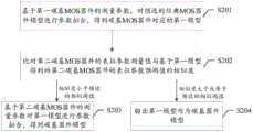
S201:基于第一碳基MOS器件的测量参数,对预选的经典MOS器件模型进行参数拟合,得到碳基MOS器件对应的第一模型。S201: Based on the measured parameters of the first carbon-based MOS device, perform parameter fitting on a preselected classical MOS device model to obtain a first model corresponding to the carbon-based MOS device.
经典MOS器件模型存储于预选的硅基集成电路设计自动化系统中,可以是硅基经典MOS器件模型。预选的硅基MOS器件与第一碳基MOS器件具有较高的相似度,硅基MOS器件与碳基MOS器件的相似度可以基于特征尺寸、器件结构、工艺特点以及应用场景等信息进行计算。The classic MOS device model is stored in the pre-selected silicon-based integrated circuit design automation system, which may be a silicon-based classic MOS device model. The preselected silicon-based MOS device has a high similarity with the first carbon-based MOS device, and the similarity between the silicon-based MOS device and the carbon-based MOS device can be calculated based on information such as feature size, device structure, process characteristics, and application scenarios.
作为示例,在参数拟合的过程中,所涉及的参数包括但不限于:例如迁移率、电容和噪声模型等控制参数;例如计算阈值和电流等直流参数;例如与器件电容相关的几何尺寸和介电常数等交流参数及电容;例如沟道长度和宽度、尺寸偏差等器件尺寸参数;例如氧化层厚度、掺杂浓度、温度等工艺参数。对第一碳基MOS器件的上述参数的测量值,也即测量参数,进行提取,并与经典MOS器件模型通过例如数据拟合(Data Fitting)算法进行参数拟合,即可得到第一碳基MOS器件对应的第一模型。As an example, in the process of parameter fitting, the parameters involved include but are not limited to: control parameters such as mobility, capacitance, and noise model; DC parameters such as calculation threshold and current; such as geometric dimensions related to device capacitance and AC parameters such as dielectric constant and capacitance; device size parameters such as channel length and width, and dimensional deviation; process parameters such as oxide layer thickness, doping concentration, and temperature. The measured values of the above parameters of the first carbon-based MOS device, that is, the measurement parameters, are extracted, and the parameters are fitted with the classic MOS device model through, for example, a data fitting (Data Fitting) algorithm, and the first carbon-based MOS device can be obtained. The first model corresponding to the MOS device.
S202:比对第二碳基MOS器件的表征参数测量值与基于第一模型得到的第二碳基MOS器件的表征参数预测值的相似度,若相似度小于预设的相似阈值,则执行S203的步骤;若相似度大于或等于预设的相似阈值,则执行S204的步骤。S202: Compare the similarity between the measured value of the characteristic parameter of the second carbon-based MOS device and the predicted value of the characteristic parameter of the second carbon-based MOS device based on the first model, and if the similarity is less than the preset similarity threshold, execute S203 step; if the similarity is greater than or equal to the preset similarity threshold, step S204 is executed.
示例性地,第二碳基MOS器件与所述第一碳基MOS器件的制造工艺相同,也即二者是特征尺寸、器件结构、工艺特点以及应用场景等信息完全相同的同一类碳基MOS器件。比对第二碳基MOS器件的表征参数测量值与基于第一模型得到的第二MOS器件的表征参数预测值的相似度,可以判断使用第一模型得到的模型参数的准确度。Exemplarily, the manufacturing process of the second carbon-based MOS device is the same as that of the first carbon-based MOS device, that is, the two are the same type of carbon-based MOS device with the same feature size, device structure, process characteristics, and application scenarios. device. Comparing the similarity between the measured value of the characteristic parameter of the second carbon-based MOS device and the predicted value of the characteristic parameter of the second MOS device obtained based on the first model, the accuracy of the model parameter obtained by using the first model can be judged.
可选地,可以将第二碳基MOS器件抽象为主要表征参数的黑盒子,重点比对第二碳基MOS器件的以下主要表征参数的测量值和预测值:开态电流Ion、关态电流Ioff、亚阈值斜率SS、阈值电压Vt、漏致势垒降低系数DIBL、沟道电阻Rch、饱和电压Vdsat、输出电阻Ro以及跨导gm,也可以比对更多表征参数的测量值和预测值。Optionally, the second carbon-based MOS device can be abstracted as a black box of main characterization parameters, and the measured and predicted values of the following main characterization parameters of the second carbon-based MOS device can be compared with focus: on-state current Ion, off-state current Ioff, subthreshold slope SS, threshold voltage Vt, leakage-induced barrier reduction coefficient DIBL, channel resistance Rch, saturation voltage Vdsat, output resistance Ro, and transconductance gm can also compare the measured and predicted values of more characterization parameters .
若比对结果为相似度小于预设的相似阈值,则表示测量值和预测值偏差较大,基于第一模型得到的预测值无法达到所需的准确度,需执行S203的步骤;若相似度大于或等于预设的相似阈值,则表示测量值和预测值偏差较小,基于第一模型得到的预测值已经达到所需的准确度,执行S204的步骤。If the comparison result is that the similarity is less than the preset similarity threshold, it means that the measured value and the predicted value have a large deviation, and the predicted value obtained based on the first model cannot reach the required accuracy, and the step of S203 needs to be performed; if the similarity If it is greater than or equal to the preset similarity threshold, it means that the deviation between the measured value and the predicted value is small, and the predicted value obtained based on the first model has reached the required accuracy, and step S204 is performed.
S203:基于第二碳基MOS器件的测量参数对第一模型进行参数拟合,得到碳基器件模型。S203: Perform parameter fitting on the first model based on the measured parameters of the second carbon-based MOS device to obtain a carbon-based device model.
具体地,得到的碳基器件模型可用于预测与第一碳基MOS器件的制造工艺相同的第三碳基MOS器件的表征参数预测值,且第三碳基MOS器件的表征参数测量值与基于碳基器件模型得到的第三碳基MOS器件的表征参数预测值的相似度大于或等于预设的相似阈值。Specifically, the obtained carbon-based device model can be used to predict the predicted value of the characteristic parameters of the third carbon-based MOS device with the same manufacturing process as the first carbon-based MOS device, and the measured value of the characteristic parameters of the third carbon-based MOS device is the same as that based on The similarity of the predicted values of the characteristic parameters of the third carbon-based MOS device obtained by the carbon-based device model is greater than or equal to a preset similarity threshold.
可选地,本步骤可多次对第一模型进行参数拟合,直至得到所需的碳基器件模型;也可以每执行一次参数拟合后,基于得到的新的器件模型比对碳基MOS器件的表征参数预测值和测量值的相似度,重复执行直至得到相似度大于或等于预设的相似阈值的碳基器件模型。Optionally, this step can perform parameter fitting on the first model multiple times until the required carbon-based device model is obtained; it is also possible to compare the carbon-based MOS based on the obtained new device model after each parameter fitting. The similarity between the predicted value and the measured value of the characteristic parameter of the device is repeated until a carbon-based device model with a similarity greater than or equal to a preset similarity threshold is obtained.
S204:输出第一模型作为碳基器件模型。S204: Outputting the first model as a carbon-based device model.
由此,本申请实施例基于测量值与预测值的对比验证结果,多次执行参数拟合,可以得到收敛性较好的碳基器件模型,并有效解决了碳基集成电路设计自动化平台在被长期使用后,碳基器件模型的预测值与实际的测量值偏差过大而无法调节的问题。Therefore, in the embodiment of the present application, based on the comparison and verification results of the measured value and the predicted value, the parameter fitting is performed multiple times, and a carbon-based device model with better convergence can be obtained, and it effectively solves the problem of the carbon-based integrated circuit design automation platform. After long-term use, the predicted value of the carbon-based device model deviates too much from the actual measured value and cannot be adjusted.
参见图3,该图为本申请实施例提供的一种碳基工艺设计工具包建立方法流程图,该方法包括:Referring to Fig. 3, this figure is a flow chart of a method for establishing a carbon-based process design toolkit provided in the embodiment of the present application, and the method includes:
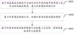
S301:基于碳基MOS器件对应的碳基工艺流程以及硅基MOS器件对应的硅基工艺流程,建立与硅基工艺流程对应的硅基工艺图层存在第一映射关系的碳基工艺图层。S301: Based on the carbon-based process flow corresponding to the carbon-based MOS device and the silicon-based process flow corresponding to the silicon-based MOS device, establish a carbon-based process layer having a first mapping relationship with the silicon-based process layer corresponding to the silicon-based process flow.
示例性地,可以基于碳基MOS器件和硅基MOS器件各自对应的工艺流程之间的差异,进行相应的对比等效处理,得到相较于硅基MOS器件对应的硅基工艺流程而言,碳基MOS器件对应的碳基工艺流程多出或缺少的工序,在碳基工艺基础图层的基础上构建碳基工艺辅助图层。碳基工艺基础图层和碳基工艺辅助图层共同组成了碳基工艺图层,碳基工艺图层可以通过第一映射关系与硅基工艺流程对应的硅基工艺图层对应起来。Exemplarily, based on the difference between the corresponding process flows of carbon-based MOS devices and silicon-based MOS devices, corresponding comparison and equivalent processing can be carried out, and compared with the corresponding silicon-based process flows of silicon-based MOS devices, Carbon-based MOS devices correspond to carbon-based processes that have more or less processes, and build a carbon-based process auxiliary layer on the basis of the carbon-based process basic layer. The carbon-based process basic layer and the carbon-based process auxiliary layer together constitute the carbon-based process layer, and the carbon-based process layer can be associated with the silicon-based process layer corresponding to the silicon-based process through the first mapping relationship.
具体地,碳基工艺流程与硅基工艺流程存在工艺步骤、工艺顺序、器件材料以及器件结构等方面的差异,二者之间的差异包括但不限于:碳基工艺可以不进行离子掺杂,即没有如硅基工艺的阱和扩散层;碳基工艺的有源区是碳纳米管层,而硅基工艺的有源区是中掺杂离子注入的区域;碳基工艺的源漏端直接是金属材料,即没有如硅基工艺的接触孔和金属等。Specifically, there are differences between the carbon-based process flow and the silicon-based process flow in terms of process steps, process sequences, device materials, and device structures. The differences between the two include but are not limited to: carbon-based processes may not be ion-doped, That is, there are no wells and diffusion layers like the silicon-based process; the active area of the carbon-based process is a carbon nanotube layer, while the active area of the silicon-based process is the region where doped ions are implanted; the source and drain of the carbon-based process are directly It is a metal material, that is, there are no contact holes and metals such as silicon-based processes.
基于上述差异以及遵循碳基工艺流程的碳基工艺基础图层,可以构建碳基工艺辅助图层。碳基工艺辅助图层包括两种类型:一类是常规的辅助层,用于方便硅基EDA工具对碳基器件电路的版图进行布尔运算处理;另一类是对照硅基工艺流程而言需要添加的工序,碳基工艺流程相比于硅基工艺流程缺少的工序会导致现有硅基EDA工具无法提取和识别碳基器件电路而出现兼容性问题。针对两种情况,分别构建不进行生产制作的碳基工艺辅助图层,以便硅基EDA工具能够正确提取和识别碳基器件电路,例如碳基MOS器件增加源漏区的接触孔这一碳基工艺辅助图层,但实际制作过程中并不在碳基MOS器件上制作源漏区的接触孔。Based on the above differences and the carbon-based process basic layer following the carbon-based process flow, a carbon-based process auxiliary layer can be constructed. There are two types of carbon-based process auxiliary layers: one is a conventional auxiliary layer, which is used to facilitate silicon-based EDA tools to perform Boolean operations on the layout of carbon-based device circuits; The added process, the lack of processes in the carbon-based process flow compared to the silicon-based process flow will cause the existing silicon-based EDA tools to be unable to extract and identify the carbon-based device circuit, resulting in compatibility issues. For the two cases, build carbon-based process auxiliary layers that are not manufactured, so that silicon-based EDA tools can correctly extract and identify carbon-based device circuits, such as carbon-based MOS devices that add contact holes in source and drain regions. The process auxiliary layer, but the contact holes of the source and drain regions are not made on the carbon-based MOS device during the actual manufacturing process.
碳基工艺图层可以通过第一映射关系与硅基工艺流程对应的硅基工艺图层对应起来,具体地,可以根据碳基工艺流程的器件材料、工艺顺序和器件特性等工艺特征,将碳基工艺图层与硅基工艺图层中的相同结构一一对应,建立第一映射关系,例如,可以将碳基工艺图层中的碳纳米管层(CNT)与硅基工艺图层中的有源区(AA/ACT)对应映射,使其符合现有的全定制设计硅基EDA工具对版图图层的基本处理规则。The carbon-based process layer can be mapped to the silicon-based process layer corresponding to the silicon-based process flow through the first mapping relationship. Specifically, the carbon-based process layer can be mapped according to the device material, process sequence, and device characteristics of the carbon-based process flow. The base process layer corresponds to the same structure in the silicon base process layer one by one, and establishes the first mapping relationship. For example, the carbon nanotube layer (CNT) in the carbon base process layer can be compared with the silicon base process layer. The corresponding mapping of the active area (AA/ACT) makes it conform to the basic processing rules of the existing full-custom design silicon-based EDA tools for the layout layer.
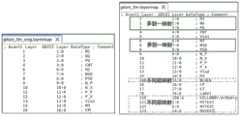
为了更好地理解该步骤,以下以碳基工艺图层中的部分图层进行说明,以下示例中,碳基工艺基础图层包括金属一层M1、N型碳纳米管晶体管栅NG、P型碳纳米管晶体管栅PG、碳纳米管层CNT、P型碳纳米管晶体管源漏区域PSD、N型碳纳米管晶体管源漏区域NSD、金属二层M2、N型碳纳米管晶体管钝化区N_P、P型碳纳米管晶体管钝化区P_P等;一类碳基工艺辅助图层包括金属文本层、布线阻挡层BLOCK、标签层Label、单元边界层CELLBNDY等;另一类碳基工艺辅助图层包括接触孔层CT和通孔一层Via1等。可以理解的是,此处仅是用于示例,碳基工艺基础图层和碳基工艺辅助图层并不限于此。参见下表1,该表为本申请实施例提供的碳基工艺图层中部分图层的实例化层名示例表。In order to better understand this step, some layers in the carbon-based process layer are described below. In the following example, the carbon-based process basic layer includes a metal layer M1, an N-type carbon nanotube transistor gate NG, and a P-type carbon nanotube transistor gate. Carbon nanotube transistor gate PG, carbon nanotube layer CNT, P-type carbon nanotube transistor source-drain region PSD, N-type carbon nanotube transistor source-drain region NSD, metal two-layer M2, N-type carbon nanotube transistor passivation region N_P , P-type carbon nanotube transistor passivation area P_P, etc.; one type of carbon-based process auxiliary layer includes metal text layer, wiring barrier layer BLOCK, label layer Label, cell boundary layer CELLBNDY, etc.; another type of carbon-based process auxiliary layer Including the contact hole layer CT and the through hole layer Via1 and so on. It can be understood that this is only an example, and the carbon-based process basic layer and the carbon-based process auxiliary layer are not limited thereto. See Table 1 below, which is an example table of instantiated layer names of some layers in the carbon-based process layer provided in the embodiment of the present application.
表1碳基工艺图层中的部分图层的实例化层名示例表Table 1 Example table of instantiated layer names of some layers in the carbon-based process layer


S302:基于第一映射关系以及碳基工艺图层,建立第一工艺设计工具包。S302: Establish a first process design toolkit based on the first mapping relationship and the carbon-based process layer.
具体地,建立碳基工艺流程对应的碳基PDK中的参数化单元(ParameterizedCell,PCell)和工艺文件(techfile/dispiay/laymap),从而得到包括碳基工艺图层、对应的参数化单元和对应的工艺文件的碳基工艺设计工具包,得到的碳基工艺设计工具包可用于硅基EDA系统。Specifically, the parameterized cell (ParameterizedCell, PCell) and process file (techfile/dispiay/laymap) in the carbon-based PDK corresponding to the carbon-based process flow are established, so as to obtain the carbon-based process layer, the corresponding parameterized cell, and the corresponding The process files of the Carbon-Based Process Design Toolkit, the resulting Carbon-Based Process Design Toolkit can be used for silicon-based EDA systems.
S303:基于第一工艺设计工具包,验证预设的碳基全定制集成电路设计流程,若验证结果为碳基工艺图层中的至少一层图层无法在碳基全定制集成电路设计流程中执行,则重新执行S301所述的步骤;若验证结果为碳基工艺图层中的全部图层均可以在碳基全定制集成电路设计流程中执行,则输出第一工艺设计工具包作为碳基工艺设计工具包。S303: Based on the first process design toolkit, verify the preset carbon-based full-custom integrated circuit design process, if the verification result is that at least one layer of the carbon-based process layer cannot be used in the carbon-based full-custom integrated circuit design process Execute, then re-execute the steps described in S301; if the verification result is that all the layers in the carbon-based process layer can be executed in the carbon-based full custom integrated circuit design process, then output the first process design toolkit as a carbon-based Process design kit.
由此,本申请实施例通过增加碳基工艺辅助图层,使得碳基工艺图层和硅基工艺图层可以通过第一映射关系对应起来,得到可以用于硅基EDA系统且通过碳基全定制集成电路设计流程的碳基工艺设计工具包。Therefore, the embodiment of the present application adds a carbon-based process auxiliary layer, so that the carbon-based process layer and the silicon-based process layer can be associated through the first mapping relationship, and can be used in a silicon-based EDA system and through a carbon-based full A carbon-based process design toolkit for custom IC design flows.
参见图4,该图为本申请实施例提供的一种碳基标准单元库模型建立方法流程图,该方法包括:Referring to Fig. 4, this figure is a flow chart of a method for establishing a carbon-based standard cell library model provided by the embodiment of the present application. The method includes:
S401:基于硅基集成电路设计自动化系统中的硅基布局布线工具对应的硅基版图层以及碳基工艺流程,建立双重图层映射文件。S401: Based on the silicon-based layout layer and the carbon-based process flow corresponding to the silicon-based layout and routing tool in the silicon-based integrated circuit design automation system, a dual-layer mapping file is established.
基于碳基工艺流程及其与硅基工艺流程之间的差异,可以构建碳基版图层,其中,碳基版图层可以包括碳基辅助版图层和碳基基础版图层。碳基辅助版图层包括两种类型:一类是常规的布尔运算识别层,方便硅基EDA工具对碳基版图层做运算处理;另一类是对照硅基工艺流程而言需要添加的工序,碳基工艺流程相比于硅基工艺流程缺少工序,导致现有硅基EDA工具无法提取和识别碳基器件电路而出现兼容性问题。针对两种情况,分别构建不进行生产制作的碳基版图层,以便硅基EDA工具能够正确提取和识别碳基器件电路,得到完整的碳基版图层,并基于碳基版图层建立碳基布局布线工艺文件(techfile)。Based on the carbon-based process flow and its difference with the silicon-based process flow, a carbon-based layout layer can be constructed, wherein the carbon-based layout layer can include a carbon-based auxiliary layout layer and a carbon-based basic layout layer. The carbon-based auxiliary plate layer includes two types: one is a conventional Boolean operation identification layer, which is convenient for silicon-based EDA tools to perform operations on the carbon-based plate layer; the other is a process that needs to be added in comparison with the silicon-based process flow, Compared with the silicon-based process flow, the carbon-based process flow lacks processes, which leads to the inability of the existing silicon-based EDA tools to extract and identify the carbon-based device circuit, resulting in compatibility problems. For the two cases, build a carbon-based layout without production, so that the silicon-based EDA tool can correctly extract and identify the carbon-based device circuit, obtain a complete carbon-based layout, and build a carbon-based layout based on the carbon-based layout Wiring process file (techfile).
为了更好地理解该步骤,以下以碳基工艺laymap文件为例进行碳基辅助版图层介绍,可以理解的是,此处仅是用于示例,碳基版图层并不限于此。如图5所示,该图为碳基工艺需要增加的两类碳基辅助版图层信息示意图,其中,左图为硅基版图层信息示意图,右图为碳基版图层信息示意图,右图中,阻挡层(Block)、标签层(Lable)、边界层(CELLBNDY)、文本层(M1TEXT/M2TEXT/M3TEXT)是一类辅助层,也即常规运算辅助版图层;碳基MOS器件的源漏区(NSD/PSD)与金属(M1/M2)之间不需要接触孔/通孔,但硅基布局布线EDA工具需要识别接触孔或通孔层才能正确提取电气关系和识别电路器件,图5中虚线框示例的接触孔(CT/Contact)、通孔层(Via1),是二类辅助层,也即碳基器件电路提取所需的辅助版图层。In order to better understand this step, the following uses the carbon-based process laymap file as an example to introduce the carbon-based auxiliary layout layer. It can be understood that this is only for example, and the carbon-based layout layer is not limited to this. As shown in Figure 5, this figure is a schematic diagram of the information of two types of carbon-based auxiliary layout layers that need to be added to the carbon-based process. , the barrier layer (Block), the label layer (Lable), the boundary layer (CELLBNDY), the text layer (M1TEXT/M2TEXT/M3TEXT) are a type of auxiliary layer, that is, the conventional operation auxiliary layout layer; the source and drain regions of carbon-based MOS devices (NSD/PSD) and metal (M1/M2) do not require contact holes/vias, but silicon-based layout and routing EDA tools need to identify contact holes or via layers to correctly extract electrical relationships and identify circuit devices, as shown in Figure 5 The contact hole (CT/Contact) and the via layer (Via1) in the dotted box example are the second type of auxiliary layer, that is, the auxiliary layout layer required for the extraction of the carbon-based device circuit.
双重图层映射文件包括符合碳基工艺流程的掩膜的第一图层映射文件以及携带碳基工艺流程对应的碳基版图层与硅基版图层的第二映射关系的第二图层映射文件。具体地,第一图层映射文件完全遵循碳基工艺掩膜层,主要针对全定制设计EDA工具与数字布局布线工具常规层(或保留层)的差异问题,进行不同图层的转换映射,便于真实碳基工艺版图的制版和流片;第二图层映射文件将碳基版图层映射到现有硅基布局布线EDA工具对应的硅基版图层,针对碳基工艺材料、工艺顺序和器件特性等方面的特征,可以将碳基基础版图层的多层映射到EDA工具的一层,也可以将碳基基础版图层的一层映射到EDA工具的多层,还可以直接增加碳基辅助版图层,从而将碳基版图层逐层与相同结构的硅基版图层对应,使其符合现有硅基EDA工具对版图层处理的基本规则,以便进行碳基芯片版图的自动化设计。The dual layer mapping file includes the first layer mapping file of the mask conforming to the carbon-based process flow and the second layer mapping file carrying the second mapping relationship between the carbon-based layer and the silicon-based layer corresponding to the carbon-based process . Specifically, the first layer mapping file completely follows the carbon-based process mask layer, and mainly aims at the difference between the full custom design EDA tool and the conventional layer (or reserved layer) of the digital layout and routing tool, and performs conversion mapping of different layers, which is convenient Plate making and tape-out of the real carbon-based process layout; the second layer mapping file maps the carbon-based layout layer to the silicon-based layout layer corresponding to the existing silicon-based layout and routing EDA tool, for carbon-based process materials, process sequences and device characteristics and other aspects, you can map the multi-layer of the carbon-based basic layout layer to the first layer of the EDA tool, or you can map the layer of the carbon-based basic layout layer to the multi-layer of the EDA tool, and you can also directly add the carbon-based auxiliary layout Layers, so that the carbon-based layout layer corresponds to the silicon-based layout layer with the same structure layer by layer, so that it conforms to the basic rules of the existing silicon-based EDA tools for layout layer processing, so as to carry out automatic design of carbon-based chip layout.
为了更好地理解该步骤,以下以碳基工艺laymap文件为例进行碳基版图层与硅基版图层的映射介绍,可以理解的是,此处仅是用于示例,碳基版图层并不限于此。如图6所示,该图为碳基版图层与硅基版图层的映射关系示意图,其中,左图为硅基版图层信息示意图,右图为碳基版图层信息示意图,例如,边界层(CELLBNDY/prBndry)在全定制设计EDA工具中是156:4,代表层号是156,层目标是4;而在数字布局布线EDA工具中,边界层(CELLBNDY/prBndry)是保留层,其层号是255层,由此,需要进行不同图层属性的转换映射。另一种类型是基于碳基工艺流程的特征,例如碳基金属一(M1)、N型碳纳米管晶体管栅(NG)、P型碳纳米管晶体管栅(PG)在同一水平面,采用同一种工艺材料(如Au),所以需要进行多到一的图层映射,以便现有硅基EDA工具进行处理。同理,还有一到多的图层映射。In order to better understand this step, the following takes the carbon-based process laymap file as an example to introduce the mapping between the carbon-based layer and the silicon-based layer. It can be understood that this is only for example, and the carbon-based layer is not limited to this. As shown in Figure 6, this figure is a schematic diagram of the mapping relationship between a carbon-based stencil layer and a silicon-based stencil layer, wherein the left figure is a schematic diagram of silicon-based stencil layer information, and the right figure is a schematic diagram of carbon-based stencil layer information, for example, the boundary layer ( CELLBNDY/prBndry) is 156:4 in the full custom design EDA tool, which means that the layer number is 156, and the layer target is 4; while in the digital layout and routing EDA tool, the boundary layer (CELLBNDY/prBndry) is a reserved layer, and its layer number It is 255 layers, so it is necessary to perform conversion mapping of different layer attributes. The other type is based on the characteristics of carbon-based process flow, such as carbon-based metal one (M1), N-type carbon nanotube transistor gate (NG), and P-type carbon nanotube transistor gate (PG). Process materials (such as Au), so many-to-one layer mapping is required for processing by existing silicon-based EDA tools. Similarly, there is one-to-many layer mapping.
S402:基于双重图层映射文件,构建双重库抽象版图库模型。S402: Based on the dual-layer mapping file, construct a dual-library abstract version library model.
具体地,双重抽象版图库模型包括符合碳基工艺流程的掩膜的第一抽象版图库模型以及携带第二映射关系的第二抽象版图库模型,其中,第一抽象版图库模型可用于生产制造碳基器件电路,但由于其完全符合碳基工艺流程,无法用于现有的硅基布局布线EDA工具;而第二抽象版图库模型经过了图层映射,可以用于现有的硅基布局布线EDA工具。Specifically, the double abstract layout library model includes a first abstract layout library model of a mask conforming to a carbon-based process flow and a second abstract layout library model carrying a second mapping relationship, wherein the first abstract layout library model can be used for manufacturing Carbon-based device circuits, but because they are fully compliant with carbon-based process flow, they cannot be used in existing silicon-based layout and routing EDA tools; and the second abstract layout library model has been layer-mapped and can be used in existing silicon-based layouts Wiring EDA tools.
S403:基于双重库抽象版图库模型以及碳基工艺流程,得到碳基标准单元库模型。S403: Obtain a carbon-based standard cell library model based on the dual-library abstract version library model and the carbon-based process flow.
具体地,可以对照碳基工艺流程完成单元Verilog模型、Liberty模型、CDL网表、符号库以及版图库等部分的构建,从而得到包括双重抽象版图库模型的碳基标准单元库模型,得到的碳基标准单元库模型可用于硅基布局布线工具。Specifically, the construction of the cell Verilog model, Liberty model, CDL netlist, symbol library, and layout library can be completed according to the carbon-based process flow, so as to obtain the carbon-based standard cell library model including the double abstract layout library model, and the obtained carbon Base standard cell library models are available for silicon place and route tools.
示例性地,得到碳基标准单元库模型之后,可以基于双重库抽象版图库模型中的第二抽象版图库模型以及第二图层映射文件进行碳基集成电路的自动布局布线并进行相应物理验证(DRC/LVS/XRC),基于双重库抽象版图库模型中的第一抽象版图库模型以及第一图层映射文件进行版图的映射和导出,从而使最后用于实际生产时显示的版图完全符合碳基工艺流程的制程掩膜。Exemplarily, after obtaining the carbon-based standard cell library model, automatic layout and routing of carbon-based integrated circuits and corresponding physical verification can be performed based on the second abstract layout library model in the double library abstract layout library model and the second layer mapping file (DRC/LVS/XRC), map and export the layout based on the first abstract layout library model in the double-library abstract layout library model and the first layer mapping file, so that the layout displayed in the final actual production is completely consistent with Process masks for carbon-based process flows.
由此,本申请实施例通过增加碳基辅助版图层,建立了双重库抽象版图库模型,使得第一抽象版图库模型用于实际的生产制造,第二抽象版图库模型用于使现有的硅基布局布线EDA工具可以识别和处理,得到了可以用于硅基EDA系统的碳基标准单元库模型。Therefore, the embodiment of the present application establishes a dual library abstract layout library model by adding a carbon-based auxiliary layout layer, so that the first abstract layout library model is used for actual production, and the second abstract layout library model is used to make the existing Silicon-based place-and-route EDA tools can identify and process, and get a carbon-based standard cell library model that can be used in silicon-based EDA systems.
参见图7,该图为本申请实施例提供的一种碳基集成电路设计自动化平台构建装置示意图,该装置包括:碳基器件模型建立模块701、碳基工艺设计工具包建立模块702、碳基标准单元库模型建立模块703以及平台构建模块704Referring to FIG. 7 , this figure is a schematic diagram of a carbon-based integrated circuit design automation platform construction device provided in the embodiment of the present application. The device includes: a carbon-based device
碳基器件模型建立模块701,用于基于碳基MOS器件的测量参数,对预选的经典MOS器件模型进行参数拟合,得到碳基MOS器件对应的碳基器件模型;经典MOS器件模型存储于预选的硅基集成电路设计自动化系统中。The carbon-based device
碳基工艺设计工具包建立模块702,用于基于碳基MOS器件对应的碳基工艺流程以及硅基MOS器件对应的硅基工艺流程,建立碳基工艺设计工具包;碳基工艺设计工具包至少包括与硅基工艺流程对应的硅基工艺图层存在第一映射关系的碳基工艺图层,碳基工艺图层包括碳基工艺基础图层和碳基工艺辅助图层。The carbon-based process design
碳基标准单元库模型建立模块703,用于基于硅基集成电路设计自动化系统中的硅基布局布线工具对应的硅基版图层以及碳基工艺流程,构建与硅基布局布线工具兼容的碳基标准单元库模型;碳基标准单元库至少包括双重库抽象版图库模型,双重库抽象版图库模型包括符合碳基工艺流程的掩膜的第一碳基抽象版图库模型和可用于硅基布局布线工具的第二碳基抽象版图库模型。The carbon-based standard cell library
平台构建模块704,用于基于碳基器件模型、碳基工艺设计工具包、碳基标准单元库模型以及硅基集成电路设计自动化系统,构建碳基集成电路设计自动化平台;碳基集成电路设计自动化平台用于进行碳基集成电路设计。The
可选地,碳基器件模型建立模块,包括:参数拟合单元,比对单元以及碳基器件模型输出单元。Optionally, the carbon-based device model building module includes: a parameter fitting unit, a comparison unit and a carbon-based device model output unit.
拟合单元,用于基于第一碳基MOS器件的测量参数,对预选的经典MOS器件模型进行参数拟合,得到碳基MOS器件对应的第一模型;经典MOS器件模型存储于预选的硅基集成电路设计自动化系统中。The fitting unit is used to perform parameter fitting on the pre-selected classic MOS device model based on the measured parameters of the first carbon-based MOS device to obtain the first model corresponding to the carbon-based MOS device; the classic MOS device model is stored in the pre-selected silicon-based Integrated circuit design automation system.
比对单元,用于比对第二碳基MOS器件的表征参数测量值与基于第一模型得到的第二碳基MOS器件的表征参数预测值的相似度;第二碳基MOS器件与第一碳基MOS器件的制造工艺相同。The comparison unit is used to compare the similarity between the measured value of the characteristic parameter of the second carbon-based MOS device and the predicted value of the predicted value of the characteristic parameter of the second carbon-based MOS device based on the first model; the second carbon-based MOS device and the first The fabrication process of carbon-based MOS devices is the same.
碳基器件模型输出单元,用于当相似度小于预设的相似阈值时,基于第二碳基MOS器件的测量参数对第一模型进行参数拟合,得到碳基器件模型;第三碳基MOS器件的表征参数测量值与基于碳基器件模型得到的第三碳基MOS器件的表征参数预测值的相似度大于或等于相似阈值,第三碳基MOS器件与第一碳基MOS器件的制造工艺相同;当相似度大于或等于相似阈值时,输出第一模型作为碳基器件模型。The carbon-based device model output unit is used to perform parameter fitting on the first model based on the measurement parameters of the second carbon-based MOS device to obtain the carbon-based device model when the similarity is less than the preset similarity threshold; the third carbon-based MOS The similarity between the measured value of the characteristic parameter of the device and the predicted value of the characteristic parameter of the third carbon-based MOS device based on the carbon-based device model is greater than or equal to the similarity threshold, and the manufacturing process of the third carbon-based MOS device and the first carbon-based MOS device Same; when the similarity is greater than or equal to the similarity threshold, output the first model as the carbon-based device model.
可选地,碳基工艺设计工具包建立模块,包括:碳基工艺图层建立单元,工艺设计工具包建立单元,流程验证单元以及碳基工艺设计工具包输出单元。Optionally, the carbon-based process design toolkit building module includes: a carbon-based process design toolkit building unit, a process design toolkit building unit, a process verification unit, and a carbon-based process design toolkit output unit.
碳基工艺图层建立单元,用于基于碳基MOS器件对应的碳基工艺流程以及硅基MOS器件对应的硅基工艺流程,建立与硅基工艺流程对应的硅基工艺图层存在第一映射关系的碳基工艺图层;碳基工艺图层包括碳基工艺基础图层和碳基工艺辅助图层。The carbon-based process layer establishment unit is used to establish the first mapping of the silicon-based process layer corresponding to the silicon-based process flow based on the carbon-based process flow corresponding to the carbon-based MOS device and the silicon-based process flow corresponding to the silicon-based MOS device The carbon-based technology layer of the relationship; the carbon-based technology layer includes the carbon-based technology basic layer and the carbon-based technology auxiliary layer.
工艺设计工具包建立单元,用于基于第一映射关系以及碳基工艺图层,建立第一工艺设计工具包。The process design toolkit establishing unit is configured to establish a first process design toolkit based on the first mapping relationship and the carbon-based process layer.
流程验证单元,用于基于第一工艺设计工具包,验证预设的碳基全定制集成电路设计流程。The process verification unit is used to verify the preset carbon-based full-custom integrated circuit design process based on the first process design toolkit.
碳基工艺设计工具包输出单元,用于当验证结果为碳基工艺图层中的至少一层图层无法在碳基全定制集成电路设计流程中执行时,重新执行建立与硅基工艺流程对应的硅基工艺图层存在第一映射关系的碳基工艺图层的步骤;当验证结果为碳基工艺图层中的全部图层均可以在碳基全定制集成电路设计流程中执行时,输出第一工艺设计工具包作为碳基工艺设计工具包。The carbon-based process design toolkit output unit is used to re-execute the establishment of a corresponding silicon-based process flow when at least one layer of the carbon-based process layer cannot be executed in the carbon-based full-custom integrated circuit design process as a verification result The silicon-based process layer has the step of the carbon-based process layer with the first mapping relationship; when the verification result is that all the layers in the carbon-based process layer can be executed in the carbon-based full-custom integrated circuit design process, the output The first process design kit serves as a carbon-based process design kit.
可选地,碳基标准单元库模型建立模块,包括:双重图层映射文件建立单元,双重库抽象版图库模型构建单元以及碳基标准单元库模型建立单元。Optionally, the carbon-based standard cell library model building module includes: a double-layer mapping file building unit, a double-library abstract version library model building unit, and a carbon-based standard cell library model building unit.
双重图层映射文件建立单元,用于基于硅基集成电路设计自动化系统中的硅基布局布线工具对应的硅基版图层以及碳基工艺流程,建立双重图层映射文件;双重图层映射文件包括符合碳基工艺流程的掩膜的第一图层映射文件以及携带碳基工艺流程对应的碳基版图层与硅基版图层的第二映射关系的第二图层映射文件。The dual-layer mapping file establishment unit is used to establish a dual-layer mapping file based on the silicon-based layout layer corresponding to the silicon-based layout and routing tool in the silicon-based integrated circuit design automation system and the carbon-based process flow; the dual-layer mapping file includes The first layer mapping file of the mask conforming to the carbon-based process flow and the second layer mapping file carrying the second mapping relationship between the carbon-based mask layer and the silicon-based mask layer corresponding to the carbon-based process flow.
双重库抽象版图库模型构建单元,用于基于双重图层映射文件,构建双重库抽象版图库模型;双重抽象版图库模型包括符合碳基工艺流程的掩膜的第一抽象版图库模型以及携带第二映射关系的第二抽象版图库模型。The double library abstract version library model construction unit is used to construct the double library abstract version library model based on the dual layer mapping file; the double abstract version library model includes the first abstract version library model of the mask conforming to the carbon-based process flow and the first abstract version library model carrying the second A second abstract version of the gallery model of the two-mapping relationship.
碳基标准单元库模型建立单元,用于基于双重库抽象版图库模型以及碳基工艺流程,得到碳基标准单元库模型;碳基标准单元库模型可用于硅基布局布线工具。The carbon-based standard cell library model building unit is used to obtain the carbon-based standard cell library model based on the dual-library abstract version library model and the carbon-based process flow; the carbon-based standard cell library model can be used for silicon-based layout and routing tools.
参见图8,该图为本申请实施例提供的一种碳基集成电路设计自动化平台示意图,该碳基集成电路设计自动化平台包括:碳基器件模型,碳基工艺设计工具包,碳基标准单元库模型,碳基集成电路设计流程包以及硅基集成电路设计自动化系统。See Figure 8, which is a schematic diagram of a carbon-based integrated circuit design automation platform provided by the embodiment of the present application. The carbon-based integrated circuit design automation platform includes: a carbon-based device model, a carbon-based process design toolkit, and a carbon-based standard unit Library model, carbon-based integrated circuit design flow package and silicon-based integrated circuit design automation system.
其中,碳基集成电流设计流程包包括碳基集成电路全定制设计流程包和碳基集成电路数字设计流程包;碳基集成电路设计自动化平台基于本申请提供的碳基集成电路设计自动化平台构建方法得到。Among them, the carbon-based integrated circuit design process package includes a carbon-based integrated circuit full-custom design process package and a carbon-based integrated circuit digital design process package; the carbon-based integrated circuit design automation platform is based on the carbon-based integrated circuit design automation platform construction method provided by this application get.
需要说明的是,本说明书中的各个实施例均采用递进的方式描述,各个实施例之间相同相似的部分互相参见即可,每个实施例重点说明的都是与其他实施例的不同之处。尤其,对于装置及平台实施例而言,由于其基本相似于方法实施例,所以描述得比较简单,相关之处参见方法实施例的部分说明即可。以上所描述的装置及平台实施例仅仅是示意性的,其中作为分离部件说明的单元可以是或者也可以不是物理上分开的,作为单元提示的部件可以是或者也可以不是物理单元,即可以位于一个地方,或者也可以分布到多个网络单元上。可以根据实际的需要选择其中的部分或者全部模块来实现本实施例方案的目的。本领域普通技术人员在不付出创造性劳动的情况下,即可以理解并实施。It should be noted that each embodiment in this specification is described in a progressive manner, the same and similar parts of each embodiment can be referred to each other, and each embodiment focuses on the differences from other embodiments. place. In particular, for the device and platform embodiments, since they are basically similar to the method embodiments, the description is relatively simple, and for relevant parts, please refer to part of the description of the method embodiments. The device and platform embodiments described above are only illustrative, and the units described as separate components may or may not be physically separated, and the components indicated as units may or may not be physical units, that is, they may be located in One place, or it can be distributed to multiple network elements. Part or all of the modules can be selected according to actual needs to achieve the purpose of the solution of this embodiment. It can be understood and implemented by those skilled in the art without creative effort.
以上所述,仅为本申请的一种具体实施方式,但本申请的保护范围并不局限于此,任何熟悉本技术领域的技术人员在本申请揭露的技术范围内,可轻易想到的变化或替换,都应涵盖在本申请的保护范围之内。因此,本申请的保护范围应该以权利要求的保护范围为准。The above is only a specific embodiment of the present application, but the protection scope of the present application is not limited thereto. Any person familiar with the technical field can easily think of changes or Replacement should be covered within the protection scope of this application. Therefore, the protection scope of the present application should be based on the protection scope of the claims.
Claims (10)
Translated fromChinesePriority Applications (1)
| Application Number | Priority Date | Filing Date | Title |
|---|---|---|---|
| CN202310357732.5ACN116306451A (en) | 2023-04-04 | 2023-04-04 | Method and related device for constructing carbon-based integrated circuit design automation platform |
Applications Claiming Priority (1)
| Application Number | Priority Date | Filing Date | Title |
|---|---|---|---|
| CN202310357732.5ACN116306451A (en) | 2023-04-04 | 2023-04-04 | Method and related device for constructing carbon-based integrated circuit design automation platform |
Publications (1)
| Publication Number | Publication Date |
|---|---|
| CN116306451Atrue CN116306451A (en) | 2023-06-23 |
Family
ID=86820527
Family Applications (1)
| Application Number | Title | Priority Date | Filing Date |
|---|---|---|---|
| CN202310357732.5APendingCN116306451A (en) | 2023-04-04 | 2023-04-04 | Method and related device for constructing carbon-based integrated circuit design automation platform |
Country Status (1)
| Country | Link |
|---|---|
| CN (1) | CN116306451A (en) |
- 2023
- 2023-04-04CNCN202310357732.5Apatent/CN116306451A/enactivePending
Similar Documents
| Publication | Publication Date | Title |
|---|---|---|
| US11188699B2 (en) | Placement and routing of cells using cell-level layout-dependent stress effects | |
| US10521535B2 (en) | Reuse of extracted layout-dependent effects for circuit design using circuit stencils | |
| US8578316B1 (en) | Methodologies for automatic 3-D device structure synthesis from circuit layouts for device simulation | |
| US9495506B2 (en) | Methods for layout verification for polysilicon cell edge structures in FinFET standard cells using filters | |
| CN104050306B (en) | Layout verification method for polycrystalline silicon cell edge structure in FinFET standard cell | |
| Scott et al. | Magic's circuit extractor | |
| US11334705B2 (en) | Electrical circuit design using cells with metal lines | |
| US10482212B2 (en) | Automated resistance and capacitance extraction and netlist generation of logic cells | |
| US8601430B1 (en) | Device matching tool and methods thereof | |
| US9934352B2 (en) | Method and system for manufacturing a semiconductor device | |
| US8627247B1 (en) | Systems and methods for fixing pin mismatch in layout migration | |
| US10223485B2 (en) | Reliability verification based on combining voltage propagation with simulation | |
| CN118194777B (en) | Layout transplanting method and device, storage medium and terminal equipment | |
| CN106897504B (en) | Method for developing IP module to form parameterized unit | |
| KR20230038538A (en) | Formation of wrap-around contacts to connect the source or drain epitaxial growth of a complementary field effect transistor (CFET) to the buried power rail (BPR) of the CFET. | |
| CN116306451A (en) | Method and related device for constructing carbon-based integrated circuit design automation platform | |
| US20180052951A1 (en) | Acceleration Of Voltage Propagation Based On Device Chain Reduction | |
| Boon et al. | Speeding Parasitic-Extraction Stage in Layout-Change-Order Validation Cycle Through Net-Tracing and Layout Trimming | |
| US8397183B2 (en) | Generation of asymmetric circuit devices | |
| Li | 45nm Extraction and verification flow with SPACE | |
| Thakkar | Study and Design of NVM Standard Cell Library |
Legal Events
| Date | Code | Title | Description |
|---|---|---|---|
| PB01 | Publication | ||
| PB01 | Publication | ||
| SE01 | Entry into force of request for substantive examination | ||
| SE01 | Entry into force of request for substantive examination |