CN1162839A - High-density integrated circuit interconnection and conductor forming method - Google Patents
High-density integrated circuit interconnection and conductor forming methodDownload PDFInfo
- Publication number
- CN1162839A CN1162839ACN97103784ACN97103784ACN1162839ACN 1162839 ACN1162839 ACN 1162839ACN 97103784 ACN97103784 ACN 97103784ACN 97103784 ACN97103784 ACN 97103784ACN 1162839 ACN1162839 ACN 1162839A
- Authority
- CN
- China
- Prior art keywords
- layer
- mentioned
- silicon nitride
- range
- insulating
- Prior art date
- Legal status (The legal status is an assumption and is not a legal conclusion. Google has not performed a legal analysis and makes no representation as to the accuracy of the status listed.)
- Granted
Links
Images


Landscapes
- Internal Circuitry In Semiconductor Integrated Circuit Devices (AREA)
- Semiconductor Memories (AREA)
Abstract
Description
Translated fromChinese本发明相关于高密度半导体电路的制造方法,特别是有关于高密度集成电路的内连线与导体制作方法。The present invention relates to a manufacturing method of a high-density semiconductor circuit, in particular to a manufacturing method of an interconnection line and a conductor of a high-density integrated circuit.
半导体科技在晶片上的电路密度已有戏剧性的增进,在半导体基板上与内的缩小元件非常靠近以及它们的装构密度显著地增加。最近的微影技术进展,例如偏移相位罩与自动对准制造程序已使元件的缩小与电路密度的增加有显著成效,这导致小于微米及超过百万个晶体管的晶片的超大型集成电路产生,因这方面的提升,一些电路元件因为它们的尺寸缩小而电性受到限制。Semiconductor technology has dramatically increased the circuit density on a wafer, the close proximity of shrinking components within a semiconductor substrate and their packaging density has increased significantly. Recent advances in lithography, such as offset phase masks and self-aligning manufacturing processes, have resulted in significant component shrinkage and increased circuit density, leading to ultra-large integrated circuits (VLSIs) with wafers smaller than microns and over a million transistors , due to this improvement, some circuit elements are electrically limited due to their shrinking size.
一种电路元件实验受到限制是在动态随机存取存储器晶片上的储存单元(storage cell),这些个别的动态随机存取存储器储存单元通常是由金氧半场效晶体管与一个电容器所组成,广泛地使用于电子工业界作为储存数据的功用。单一的动态随机存取存储器以电荷储存一位的数据于电容器上。与半导体基板接触而金属化称为接触金属化,在MOS元件多晶硅膜被金属化作为栅极以及MOS元件的内连线,未来不能将接触金属化及第一阶段的内连线(也就是基板上的MOS)缩小是缩小DRAM及其他元件例如MOS与双极性元件的主要障碍,因增加动态随机存取存储器的装构密度而减少存储器的表面积因此而降低晶体单元的性能是一个严重的障碍。因此为得半导体记忆元件的高装构密度,形成较小的第一阶段接触与第一阶段内连线问题和因而降低晶体单元的性能问题必须解决。One type of circuit element experiment is limited to storage cells on DRAM chips. These individual DRAM storage cells are usually composed of metal oxide semiconductor field effect transistors and a capacitor. They are widely used It is widely used in the electronics industry as a function of storing data. A single DRAM stores one bit of data as an electric charge on a capacitor. Metallization in contact with the semiconductor substrate is called contact metallization. The polysilicon film of the MOS element is metallized as the gate and the interconnection of the MOS element. In the future, the contact metallization and the first stage of the interconnection (that is, the substrate MOS) shrinking is the main obstacle to shrinking DRAM and other devices such as MOS and bipolar devices. The reduction of the surface area of the memory due to the increase in the density of the dynamic random access memory and thus the performance of the crystal unit is a serious obstacle. . Therefore, in order to obtain a high packing density of the semiconductor memory device, the problem of forming smaller first-stage contacts and first-stage interconnections and thus reducing the performance of the crystal unit must be solved.
以下文献显示相关的制造程序:“CVD SiNx Anti-Reflective Coating for Suo-0.5μm Lithograpy”,T.P.Ong et al.,1995 Symposiumon VLSI Technology Digest of Technical paper,(o-7803-2602-4/95)p.73-74;“Selective dry etching in a highdensity plasma for 0.5 complementary mental-oxide-semiconductor technology”,by J.Givens et al.,Vac.Sci.Technol.B12(1),Jan/Feb 1994,p.427-432;and“High Selectivity Silicon Nitride Etch for Sub-Half Micron Devices”,by Karen Reinhard et al.,LamResearch Corp.,Taiwan Technical Symposium,November,15,1994,然而许多先前技术方法需较多制造程序步骤或平坦化结构,使得制造程序复杂和成本较高。另外,其他制造程序方法依靠蚀刻技术及预先设定蚀刻深度然而此控制制作环境上十分困难。例如,电浆蚀刻过程的真或假气体外漏,来自泵和负载效应之后蒸气,这些将改变制造程序真空腔的化学蚀刻环境,造成蚀刻时间不易掌握,因此发展制造程序愈简单愈好并且提供不需临界深度的蚀刻是急需的。The following literature shows the relevant fabrication procedure: "CVD SiNx Anti-Reflective Coating for Suo-0.5μm Lithograpy", T.P.Ong et al., 1995 Symposium on VLSI Technology Digest of Technical paper, (o-7803-2602-4/95)p .73-74; "Selective dry etching in a high density plasma for 0.5 complementary mental-oxide-semiconductor technology", by J.Givens et al., Vac.Sci.Technol.B12(1), Jan/Feb 1994, p. 427-432; and "High Selectivity Silicon Nitride Etch for Sub-Half Micron Devices", by Karen Reinhard et al., LamResearch Corp., Taiwan Technical Symposium, November, 15, 1994, however many prior art methods require more manufacturing procedures steps or planarization structures, making the manufacturing process complex and costly. In addition, other manufacturing process methods rely on etching technology and preset etching depth, but it is very difficult to control the manufacturing environment. For example, the true or false gas leakage in the plasma etching process, the vapor from the pump and the load effect, these will change the chemical etching environment of the vacuum chamber of the manufacturing process, making it difficult to control the etching time, so the simpler the development of the manufacturing process, the better and provide Etching without a critical depth is highly desired.
发展能降低制造成本且提升元件合格率的内连线与导体是一项挑战,特别是发展减少光阻步骤之法及提供最大合格率的最大制造程序限度,典型的在制造过程形成导体内连线于位元线和接触窗需要两道罩幕与蚀刻,另外导体接触与电极接触不是自行对准而限制其微小化,通过厚的绝缘层的接触窗产生高的方位比率(大于三)而造成接触蚀刻困难及蚀刻缺乏降低合格率。不会受微影技术限制的内连线尺寸制造程序的发展是另一项挑战。It is a challenge to develop interconnects and conductors that can reduce manufacturing costs and improve component yield, especially the development of methods that reduce photoresist steps and provide maximum yield. The line between the bit line and the contact window requires two masks and etching. In addition, the conductor contact and the electrode contact are not self-aligned to limit their miniaturization. The contact window through the thick insulating layer produces a high orientation ratio (greater than three) and thus Cause contact etching difficulties and lack of etching to reduce the pass rate. The development of interconnect-scale fabrication processes that are not limited by lithography is another challenge.
本发明的主要目的为提供一种能克服微影技术限制尺寸且减少罩幕步骤的有内连线和导体的集成电路制造方法。The main purpose of the present invention is to provide a method of manufacturing integrated circuits with interconnection lines and conductors which can overcome the size limitation of lithography technology and reduce masking steps.
本发明的次一目的为提供一种具有高密度接触窗形成及内连线的集成电路制造方法。Another object of the present invention is to provide an integrated circuit manufacturing method with high-density contact opening and interconnection.
本发明的另一目的为提供一种具有高密度与低成本、简易制造程序、大的制造程序窗口的电容的动态随机存取记忆元件的制造方法。Another object of the present invention is to provide a method for manufacturing a capacitive dynamic random access memory device with high density and low cost, simple manufacturing process, and large manufacturing process window.
为完成上述的目的本发明提供一种新的具有高密度第一阶段接触与第一阶段内连线的半导体元件制造方法。此目的由下列步骤得到:(1)形成绝缘的帽盖其顶端具有反反光性质的栅极电极与第一阶段内连线(2)使用高选择性的氮化硅以定义该绝缘帽盖(3)使用栅极电极上和第一绝缘层上的绝缘间隙壁形成自行对准第一与第二阶段的基板接触。In order to achieve the above objectives, the present invention provides a new semiconductor device manufacturing method with high-density first-stage contacts and first-stage interconnections. This object is achieved by the following steps: (1) forming an insulating cap whose top has a reflective gate electrode and a first-stage interconnection (2) using highly selective silicon nitride to define the insulating cap ( 3) Forming self-aligned first and second stage substrate contacts using insulating spacers on the gate electrode and on the first insulating layer.
简而言的,具有元件区与间隙壁绝缘区形成的半导体基板上的内连线制造方法,包括下列步骤:提供一间隙壁栅极电极于元件区上。在栅极电极与导电结构的顶部表面形成由反反射氮化硅膜构成的第一绝缘帽盖层,接着由氮化硅组成的第一绝缘间隙壁形成于栅极电极的侧壁与导电结构的侧壁上。形成顶部绝缘层覆盖于栅极电极上的第一绝缘帽盖层,接着第一多晶硅层30、介电层26及第二绝缘帽盖层沉积于整个基板表面,定义光罩及选择性蚀刻第二绝缘层、介电层和栅极电极间的第一多晶硅层之上部形成具有第一侧壁的开孔。第二绝缘间隙壁形成于第一开孔的第一侧壁上,一顶部拴柱填满第一开孔形成接触至底部的拴柱形成通至源极的内连线。Briefly, the method for fabricating an interconnect on a semiconductor substrate with a device region and a spacer insulating region includes the following steps: providing a spacer gate electrode on the device region. A first insulating capping layer composed of an anti-reflective silicon nitride film is formed on the top surface of the gate electrode and the conductive structure, and then a first insulating spacer composed of silicon nitride is formed on the sidewall of the gate electrode and the conductive structure on the side wall. Form the first insulating capping layer with the top insulating layer covering the gate electrode, then the first polysilicon layer 30, the
本发明的制造程序有许多超越先前技术的优点,第一,本发明的自行对准制造程序利用两组侧壁间隙壁使有较宽的接触开窗以利蚀刻形成接触窗(contact hole),另外绝缘之间隙壁使其有小的接触窗方向比例,因此减小晶体单元受微影的限制。第一与第二绝缘帽盖层有反反射涂布能增进微影的性能使其能定义更小的接触窗。第三,本法在同个光罩步骤同时定义源极与漏极减少光罩步骤。最后,高选择性与高密度电浆蚀刻制造程序增进接触窗与储存电极的准确性。The manufacturing process of the present invention has many advantages over the prior art. First, the self-aligning manufacturing process of the present invention utilizes two sets of sidewall spacers to enable wider contact openings to facilitate etching to form contact holes. In addition, the insulating spacer makes it possible to have a small proportion of the contact window direction, thereby reducing the limitation of the crystal unit by lithography. The anti-reflective coating of the first and second insulating capping layers can improve the performance of lithography so that smaller contact windows can be defined. Third, the method defines both source and drain reduction mask steps in the same mask step. Finally, high-selectivity and high-density plasma etching processes improve the accuracy of contact windows and storage electrodes.
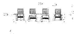
图1至图9为本发明的具有堆叠式电容的动态随机存取存储器的制造程序方法的截面图。1 to 9 are cross-sectional views of the manufacturing process of the DRAM with stacked capacitors according to the present invention.
本发明将配合图示详加以说明。本发明提供形成缩小的内连线的形成方法,另外本发明的方法可形成具小尺寸、高性能且易于制造的电容记忆单元。首先,形成场氧化区及场效晶体管结构,为了使更能了解本发明的制造程序只能详加以说明。第二使用两组间隙壁与两个反反射的氮化硅帽盖层定义内连线将由后详述。另外,基板表面意义是包括各层的表面顶部或半导体基板上的形成结构。The invention will be described in detail with reference to the drawings. The invention provides a method for forming a reduced interconnection line. In addition, the method of the invention can form a capacitive memory unit with small size, high performance and easy manufacture. First, the formation of the field oxide region and the structure of the field effect transistor can only be described in detail in order to better understand the manufacturing process of the present invention. The second method uses two sets of spacers and two anti-reflective silicon nitride capping layers to define interconnect lines, which will be described in detail later. In addition, the meaning of the substrate surface includes the surface top of each layer or the formation structure on the semiconductor substrate.
如第1图所示,本法首先在基板中有晶体管元件于其上及绝缘区域4围绕的元件区制造一电容,此绝缘区域4也就是场氧化层4形成于半导体基板上用以定义主动区与绝缘区。较佳的基板为晶面是(100)的P型单晶硅,一十分厚的场氧化层4形成在主动区的周围作为隔离电性之用,此场氧化层由沉积于主动元件区域的厚的氧化硅(氧化垫)与更厚形成氧化位障的氮化硅层为罩幕然后以氧化所形成,较佳的厚度3000至5000埃。As shown in Figure 1, this method firstly manufactures a capacitor in the element area surrounded by the transistor element and the
再以习用的湿蚀刻去除氧化硅位障与氧化垫后半导体晶体管元件形成于主动区域,最常用于动态随机存取存储器的元件为MOSFET,此元件首先以热氧化在主动区域形成薄的栅极氧化层3,较佳的厚度为70至90埃。Then the silicon oxide barrier and oxide pad are removed by conventional wet etching, and the semiconductor transistor element is formed in the active area. The most commonly used element for dynamic random access memory is MOSFET. This element is firstly formed with a thin gate in the active area by thermal oxidation. The
已掺杂的多晶硅层6与栅极介电层10沉积于基板2上,该多晶硅层6为栅极且可以具有硅化金属,栅极介电层可由氧化硅形成,栅极介电层厚度范围为200至1000埃。A doped
如第1图所示,第一绝缘帽盖层12形成于栅极绝缘层10之上,帽盖层是栅极之上层或是用来做蚀刻位障的接触结构,此第一绝缘帽盖层12是由具反反射性质的氮化硅形成较佳,减少由帽盖层的反射的反反射性质可增进微影的解析度。氮化硅第一帽盖层12用SiH2Cl2与氨反应以LPCVD沉积,厚度较佳的范围是200至2000埃,1000埃更好,第一帽盖层12消光系数(K)介于0.3至0.5之间,LPCVD制造程序的SiH2Cl2与氨比例约为1∶2与1∶4之间1∶3较佳,反应压力范围约为100至500毫托耳,以400毫托耳较佳,反应温度为750℃至850℃之间以780℃较佳。As shown in FIG. 1, a first
第一绝缘帽盖层12亦可由TEOS,SiH4,NH3以反应温度为750℃至850℃之间,反应压力范围约为100至500毫托耳利用LPCVD沉积形成SiOxNyH。第一绝缘帽盖层12由SiOxNyH形成,厚度范围约为200至2000埃。The first insulating
接着以微影与蚀刻技术定义栅极氧化层3、导电层6、栅极介电层10、与第一绝缘帽盖层12以形成栅极电极与导电结构。导电结构形成于场氧化区上作为字语线栅极电极形成于基板表面做为在DRAM或其他元件的晶体管一部分。Then, the
定义一光罩于第一绝缘帽盖层12上及蚀刻底层形成栅极电极与导电结构,蚀刻剂对氮化硅比对二氧化硅有高的选择性用以蚀刻第一绝缘帽盖层12,此高选择性的蚀刻具有两步骤:主要蚀刻与过度蚀刻步骤,主要蚀刻的压力范围约为280至320毫托耳之间,功率为250至300瓦特之间,电极之间隙壁为0.7至0.9微米之间,SF6的流量为60-80sccm,CHF3的流量为9-11sccm,He的流量为240-260sccm,过度蚀刻步骤的压力范围约为725与775毫托耳之间,功率为180至200瓦特之间,电极之间隙壁为0.9-1.1微米之间,SF6的流量为110-130sccm,CHF3的流量为9-11sccm,He的流量为18-22sccm,此高选择性高密度的电浆蚀刻制造程序增进接触窗的准确性及有较小尺寸的内连线。栅极介电层10、导电层6以及栅极氧化层3使用同一罩幕蚀刻。Define a photomask on the first insulating
接着形成MOSFET的N通道轻微掺杂源极/漏极(未显示),使用N型离子植入,例如植入砷或磷穿过栅极电极6之间隙壁形成轻微掺杂源极/漏极。典型的掺杂可以用磷P31,剂量为1E13-1E14atoms/cm2,能量为30-80KeV。Next, form the N-channel lightly doped source/drain of the MOSFET (not shown), using N-type ion implantation, such as implanting arsenic or phosphorus through the spacer of the
参看第2图,形成轻重掺杂源极/漏极之后第一绝缘间隙壁18形成于栅极电极的侧壁,此第一绝缘间隙壁18是以LPCVD沉积氮化硅形成,厚度介于200-1000埃之间,以500较佳。Referring to FIG. 2, after the lightly and heavily doped source/drain is formed, the first insulating
栅极电极间的距离范围为0.25-0.4微米之间,第一绝缘间隙壁间的较佳距离为0.2-0.35微米之间。The distance between the gate electrodes is in the range of 0.25-0.4 microns, and the preferred distance between the first insulating spacers is in the range of 0.2-0.35 microns.
MOSFET的源极/漏极区16、14于第一绝缘间隙壁之间植入N型的离子,例如砷(As)75以形成浓掺杂的源极/漏极(源极为接触电极),此掺杂过程通常是穿透过一厚度为200-300埃的氧化硅层来完成,以减小通道的掺杂及防止被金属和其他杂质的污染。典型的剂量为2E15-1E16atoms/cm2,植入能量为20-70Kev。The source/
如第3C图所示,第二栅极电极的顶部覆盖顶部绝缘层20,此绝缘层20使用栅极电极的顶部表面与场氧化层4上的导电结构齐平,绝缘层20的厚度范围是100-1000埃,此氧化硅顶部绝缘层最好是由氧化硅、TEOS、BPSG、PSG所组成且最好是由硼磷硅玻璃所组成。As shown in FIG. 3C, the top of the second gate electrode covers the top insulating
参阅第3A-3C图,顶部绝缘层以下述的步骤完成。如第3A图,氧化层20B以TEOS形成氧化物,接着平坦层20A覆盖于整个基板之上,此平坦层20A以硼磷硅玻璃组成较佳且厚度介于1000-5500埃之间。硼磷硅玻璃层以TEOS(tetraethylorthosilicate)为反应物质用低温化学气相沉积(LPCVD)方式完成,在形成硼磷硅玻璃的过程中加入硼与磷,接着以温度850℃于此平坦层施以热处理三十分钟以形成流动与平坦化,此BPSG层20A最好以回蚀刻处理使其厚度为3500-4500埃之间。Referring to Figures 3A-3C, the top insulating layer is completed in the following steps. As shown in FIG. 3A , the
参阅第3B图,平坦层20A与氧化层20B已被回蚀刻。接着于栅极电极与导电结构上覆盖光罩21,如第3C图所示,平坦层20A与氧化层20B被蚀刻形成在栅极电极上的顶部绝缘层20,另外导电结构上也许有顶部绝缘层20的残留,此氧化帽盖层20十分重要,因为其将下层平坦化及增进后继的复晶硅的蚀刻。Referring to FIG. 3B, the
如第4图所示,在上述的结果表面接着形成其他层,如第二多晶硅层22、硅化钨层24、介电层26、第二绝缘帽盖层28。第二多晶硅层22在蚀刻后的厚度最佳为1000-6000埃,更好为1500埃。硅化钨层24形成于第二复晶奎层22之上以增进第二多晶硅层22的导电度,以SiH4/WF6或SiCl2H2/WF6以CVD方式沉积形成。As shown in FIG. 4 , other layers, such as a
介电层26较佳的厚度为500-2000埃的范围,以1000埃更佳以及利用TEOS氧化物制造程序形成,例如以tetraethylorthosilicate于低压中温度650℃至750℃以化学气相沉积及沉积氧化硅反应完成。The preferred thickness of the
第二绝缘帽盖层28以氮化硅或二氧化硅形成较佳,使用SiH2Cl2与氨反应以低压化学气相沉积形成反反射的沉积,第二绝缘帽盖层28厚度范围为600-1800埃,消光系数约为0.3至0.5之间。The second insulating capping
如第4图所示,选择性蚀刻第二绝缘帽盖层28与介电层26最少要覆盖源极16,覆盖第二复晶层22的较上部分以蚀刻方式形成底部电极栓柱30B与漏极14接触,此蚀刻形成具第一侧壁的第一开孔32(也就是内连线开孔)。多晶硅区域30C形成于场氧化区域之上4。As shown in FIG. 4, the selective etching of the second insulating capping
第二绝缘帽盖层28以形成第一绝缘帽盖层相同的高选择性蚀刻形成如上所述。另外选择性蚀刻能定义比传统的氮化硅制造程序更小的内连线。The second insulating capping
介电层26是以传统对多晶硅有高选择性的蚀刻,接着蚀刻覆盖于源极16上的第二多晶硅层22的较上部份,此形成位于源极16上的底部栓柱30A,底部栓的厚度范围为0至7000埃,更佳为3000埃。
如第5图所示,第二绝缘间隙壁34形成于第一开孔32的第一侧壁上,第二绝缘层(未示出)形成覆盖于上述结果的表面,接着以非等向性蚀刻,此第二绝缘层间隙壁34以TEOS制造程序以氧化硅形成,第二绝缘层的厚度范围为200-1500埃之间更佳为1000埃。As shown in FIG. 5, a second insulating
如第6图所示,顶部电极栓柱36形成填满于第一开孔32以及形成与底部电极栓柱30A接触因此形成储存电极30A36。顶部电极栓柱36的厚度范围为2000至埃10000之间,更佳为7000埃,顶部电极栓柱36以掺杂的多晶硅或是多晶硅化金属例如硅化钨形成,顶部电极栓柱36的杂质浓度范围为1E19-1E22atoms/cm2。As shown in FIG. 6 , the
如第7图所示,电容介电层38形成覆盖于储存电极36之上,介电层物质36可以用任何高介电常数、连续及无小孔的物质,此介电层36以氮化硅、氧化物/氮化物/氧化物(ONO)薄膜、氧化氮或氧化硅物质形成,以氧化物/氮化物/氧化物(ONO)较佳,厚度范围为30至100埃,以55埃较佳,以直接毯覆式回蚀刻制造程序蚀刻电极36间的电容介电质38。As shown in Figure 7, the
顶部电极40接着覆盖于介电层38上形成如第8图所示。此藉由掺杂导电层于基板上完成。以已掺杂的复晶层或以离子植入的复晶层得到适当掺杂的复晶层,顶部电极40的适当厚度为500-2000埃,较佳为1000埃,顶部电极40以复晶型硅掺杂杂质形成较佳,顶部电极/导电层的杂质浓度为1E19-1E22atoms/cm2以1E22atoms/cm2较佳。在顶部电极40上形成顶部绝缘层50与金属层52完成DRAM单元的制作如第9图。A
本发明的形成内连线及缩小记忆单元方法比传统方法有更多的利益,第一,本发明的自行对准制造程序使用两组间隙壁18、34使得有宽的制造程序窗口供蚀刻形成接触窗32绝缘间隙壁使得有小的接触窗方向比例。利用本发明接触窗的形成不用光罩及平坦层其将自行对准形成,藉由去除平坦化的氧化层将得到小方向比例。该特殊的第一与第二绝缘帽盖层12、28以反反射沉积物质组成能增进微影的品质而有较小的接触窗。第三,此方法减少光罩的步骤定义源极与漏极接触30A、36、30B。最后,高选择性的氮化硅蚀刻制造程序增进接触窗与储存电极的准确性,再着绝缘顶层20提供平滑的最后表面,此将提供较平滑的表面以利于后继的膜层覆盖以增进合格率。The method of forming interconnection lines and shrinking memory cells of the present invention has more benefits than conventional methods. First, the self-aligned manufacturing process of the present invention uses two sets of
本发明已经以较佳实施例说明如上,然其并非用以限定本发明精神与发展实体仅止于此一实施例,而熟悉此领域技艺者,在不脱离本发明的精神范围内,当可作少许更改,其专利保护范围更当视后附的权利要求及其等同领域而定。The present invention has been described as above with a preferred embodiment, but it is not intended to limit the spirit and development of the present invention to this embodiment, and those who are familiar with this field can do it without departing from the spirit of the present invention. With a few changes, the scope of patent protection should be determined by the appended claims and their equivalent fields.
Claims (24)
Priority Applications (1)
| Application Number | Priority Date | Filing Date | Title |
|---|---|---|---|
| CN97103784ACN1056469C (en) | 1997-04-15 | 1997-04-15 | Method for forming high-density integrated circuit interconnection |
Applications Claiming Priority (1)
| Application Number | Priority Date | Filing Date | Title |
|---|---|---|---|
| CN97103784ACN1056469C (en) | 1997-04-15 | 1997-04-15 | Method for forming high-density integrated circuit interconnection |
Publications (2)
| Publication Number | Publication Date |
|---|---|
| CN1162839Atrue CN1162839A (en) | 1997-10-22 |
| CN1056469C CN1056469C (en) | 2000-09-13 |
Family
ID=5166879
Family Applications (1)
| Application Number | Title | Priority Date | Filing Date |
|---|---|---|---|
| CN97103784AExpired - LifetimeCN1056469C (en) | 1997-04-15 | 1997-04-15 | Method for forming high-density integrated circuit interconnection |
Country Status (1)
| Country | Link |
|---|---|
| CN (1) | CN1056469C (en) |
Cited By (1)
| Publication number | Priority date | Publication date | Assignee | Title |
|---|---|---|---|---|
| CN102879556A (en)* | 2012-09-25 | 2013-01-16 | 中国电子科技集团公司第四十九研究所 | Biochip with constant volume and preparation method thereof |
Family Cites Families (1)
| Publication number | Priority date | Publication date | Assignee | Title |
|---|---|---|---|---|
| KR0140720B1 (en)* | 1995-03-29 | 1998-06-01 | 김주용 | Semiconductor contact and manufacturing method thereof |
- 1997
- 1997-04-15CNCN97103784Apatent/CN1056469C/ennot_activeExpired - Lifetime
Cited By (1)
| Publication number | Priority date | Publication date | Assignee | Title |
|---|---|---|---|---|
| CN102879556A (en)* | 2012-09-25 | 2013-01-16 | 中国电子科技集团公司第四十九研究所 | Biochip with constant volume and preparation method thereof |
Also Published As
| Publication number | Publication date |
|---|---|
| CN1056469C (en) | 2000-09-13 |
Similar Documents
| Publication | Publication Date | Title |
|---|---|---|
| US5710073A (en) | Method for forming interconnections and conductors for high density integrated circuits | |
| US5607879A (en) | Method for forming buried plug contacts on semiconductor integrated circuits | |
| JP4302785B2 (en) | Method of manufacturing high density integrated circuit with oxide and polysilicon spacers | |
| KR100320332B1 (en) | Semiconductor device and manufacturing method thereof | |
| KR100242352B1 (en) | Method of fabricating a self-aligned contact hole for a semiconductor device | |
| US5483104A (en) | Self-aligning contact and interconnect structure | |
| US5780338A (en) | Method for manufacturing crown-shaped capacitors for dynamic random access memory integrated circuits | |
| US5436188A (en) | Dram cell process having elk horn shaped capacitor | |
| US8026542B2 (en) | Low resistance peripheral local interconnect contacts with selective wet strip of titanium | |
| US5874359A (en) | Small contacts for ultra large scale integration semiconductor devices without separation ground rule | |
| US6707088B2 (en) | Method of forming integrated circuitry, method of forming a capacitor, method of forming DRAM integrated circuitry and DRAM integrated category | |
| US5497016A (en) | Stacked dram poly plate capacitor | |
| US5480837A (en) | Process of making an integrated circuit having a planar conductive layer | |
| JPH08250677A (en) | Semiconductor memory device and manufacturing method thereof | |
| US5429979A (en) | Method of forming a dram cell having a ring-type stacked capacitor | |
| US5498561A (en) | Method of fabricating memory cell for semiconductor integrated circuit | |
| US6852579B2 (en) | Method of manufacturing a semiconductor integrated circuit device | |
| US5501998A (en) | Method for fabricating dynamic random access memory cells having vertical sidewall stacked storage capacitors | |
| US6746952B2 (en) | Diffusion barrier layer for semiconductor wafer fabrication | |
| US5580806A (en) | Method of fabricating a buried contact structure for SRAM | |
| US5536673A (en) | Method for making dynamic random access memory (DRAM) cells having large capacitor electrode plates for increased capacitance | |
| US5457065A (en) | method of manufacturing a new DRAM capacitor structure having increased capacitance | |
| US5604659A (en) | Microelectronic device with centered storage capacitor cavity sized less than feature size | |
| US5946568A (en) | Self aligned method of fabricating a DRAM with improved capacitance | |
| US5534457A (en) | Method of forming a stacked capacitor with an "I" shaped storage node |
Legal Events
| Date | Code | Title | Description |
|---|---|---|---|
| C10 | Entry into substantive examination | ||
| SE01 | Entry into force of request for substantive examination | ||
| C06 | Publication | ||
| PB01 | Publication | ||
| C14 | Grant of patent or utility model | ||
| GR01 | Patent grant | ||
| ASS | Succession or assignment of patent right | Owner name:TAIWEN INTEGRATED CIRCUIT MANUFACTURE CO., LTD. Free format text:FORMER OWNER: WORLD ADVANCED INTEGRATED CIRCUIT STOCK-SHARING CO., LTD. Effective date:20110406 | |
| C41 | Transfer of patent application or patent right or utility model | ||
| COR | Change of bibliographic data | Free format text:CORRECT: ADDRESS; FROM: 000000 TAIWAN, CHINA TO: 000000 HSINCHU CITY, TAIWAN, CHINA | |
| TR01 | Transfer of patent right | Effective date of registration:20110406 Address after:000000 Hsinchu, Taiwan, China Patentee after:Taiwan Semiconductor Manufacturing Co., Ltd. Address before:000000 Taiwan, China Patentee before:World Advanced Integrated circuit stock-sharing Co., Ltd. | |
| CX01 | Expiry of patent term | Granted publication date:20000913 | |
| CX01 | Expiry of patent term |