CN116266020A - Packaging method of silicon-based liquid crystal chip and chip - Google Patents
Packaging method of silicon-based liquid crystal chip and chipDownload PDFInfo
- Publication number
- CN116266020A CN116266020ACN202111547515.XACN202111547515ACN116266020ACN 116266020 ACN116266020 ACN 116266020ACN 202111547515 ACN202111547515 ACN 202111547515ACN 116266020 ACN116266020 ACN 116266020A
- Authority
- CN
- China
- Prior art keywords
- liquid crystal
- wafer substrate
- area
- sealant
- glass cover
- Prior art date
- Legal status (The legal status is an assumption and is not a legal conclusion. Google has not performed a legal analysis and makes no representation as to the accuracy of the status listed.)
- Pending
Links
Images


Classifications
- G—PHYSICS
- G02—OPTICS
- G02F—OPTICAL DEVICES OR ARRANGEMENTS FOR THE CONTROL OF LIGHT BY MODIFICATION OF THE OPTICAL PROPERTIES OF THE MEDIA OF THE ELEMENTS INVOLVED THEREIN; NON-LINEAR OPTICS; FREQUENCY-CHANGING OF LIGHT; OPTICAL LOGIC ELEMENTS; OPTICAL ANALOGUE/DIGITAL CONVERTERS
- G02F1/00—Devices or arrangements for the control of the intensity, colour, phase, polarisation or direction of light arriving from an independent light source, e.g. switching, gating or modulating; Non-linear optics
- G02F1/01—Devices or arrangements for the control of the intensity, colour, phase, polarisation or direction of light arriving from an independent light source, e.g. switching, gating or modulating; Non-linear optics for the control of the intensity, phase, polarisation or colour
- G02F1/13—Devices or arrangements for the control of the intensity, colour, phase, polarisation or direction of light arriving from an independent light source, e.g. switching, gating or modulating; Non-linear optics for the control of the intensity, phase, polarisation or colour based on liquid crystals, e.g. single liquid crystal display cells
- G02F1/133—Constructional arrangements; Operation of liquid crystal cells; Circuit arrangements
- G02F1/1333—Constructional arrangements; Manufacturing methods
- G02F1/1339—Gaskets; Spacers; Sealing of cells
- G—PHYSICS
- G02—OPTICS
- G02F—OPTICAL DEVICES OR ARRANGEMENTS FOR THE CONTROL OF LIGHT BY MODIFICATION OF THE OPTICAL PROPERTIES OF THE MEDIA OF THE ELEMENTS INVOLVED THEREIN; NON-LINEAR OPTICS; FREQUENCY-CHANGING OF LIGHT; OPTICAL LOGIC ELEMENTS; OPTICAL ANALOGUE/DIGITAL CONVERTERS
- G02F1/00—Devices or arrangements for the control of the intensity, colour, phase, polarisation or direction of light arriving from an independent light source, e.g. switching, gating or modulating; Non-linear optics
- G02F1/01—Devices or arrangements for the control of the intensity, colour, phase, polarisation or direction of light arriving from an independent light source, e.g. switching, gating or modulating; Non-linear optics for the control of the intensity, phase, polarisation or colour
- G02F1/13—Devices or arrangements for the control of the intensity, colour, phase, polarisation or direction of light arriving from an independent light source, e.g. switching, gating or modulating; Non-linear optics for the control of the intensity, phase, polarisation or colour based on liquid crystals, e.g. single liquid crystal display cells
- G02F1/133—Constructional arrangements; Operation of liquid crystal cells; Circuit arrangements
- G02F1/1333—Constructional arrangements; Manufacturing methods
- G02F1/133351—Manufacturing of individual cells out of a plurality of cells, e.g. by dicing
Landscapes
- Physics & Mathematics (AREA)
- Nonlinear Science (AREA)
- Mathematical Physics (AREA)
- Chemical & Material Sciences (AREA)
- Crystallography & Structural Chemistry (AREA)
- General Physics & Mathematics (AREA)
- Optics & Photonics (AREA)
- Liquid Crystal (AREA)
- Engineering & Computer Science (AREA)
- Manufacturing & Machinery (AREA)
Abstract
Translated fromChinese
Description
Translated fromChinese技术领域technical field
本申请属于半导体器件封装领域,具体涉及一种硅基液晶芯片的封装方法及芯片。The application belongs to the field of packaging of semiconductor devices, and in particular relates to a method for packaging a silicon-based liquid crystal chip and the chip.
背景技术Background technique
随着光电、微电制造工艺技术的飞速发展,芯片元件的封装形式也不断得到改进。不同的封装技术在制造工序和工艺方面差异很大,对芯片的生产良率以及芯片性能的发挥也起到至关重要的作用。With the rapid development of photoelectric and microelectronic manufacturing technology, the packaging form of chip components has also been continuously improved. Different packaging technologies have great differences in manufacturing processes and processes, which also play a vital role in the production yield of chips and the performance of chips.
现有的封装方法一般采用框胶对液晶进行封装,这样会导致芯片的管脚和切割区域和玻璃基板之间形成有空腔,在后续的工艺中易损害芯片上的管脚区,从而导致芯片的封装良率大大降低。Existing packaging methods generally use frame glue to package liquid crystals, which will cause cavities to be formed between the pins of the chip and the cutting area and the glass substrate, which will easily damage the pin area on the chip in the subsequent process, resulting in The packaging yield of the chip is greatly reduced.
发明内容Contents of the invention
为解决上述技术问题,本申请提供一种硅基液晶芯片的封装方法及芯片,能够提升芯片的封装良率。In order to solve the above technical problems, the present application provides a liquid crystal on silicon chip packaging method and the chip, which can improve the packaging yield of the chip.
为解决上述技术问题,本申请提供一种硅基液晶芯片的封装方法,用于封装硅基液晶芯片,且该硅基液晶芯片包括玻璃盖板、晶圆基板、框胶和液晶,上述晶圆基板上定义有管脚区和切割区,上述封装方法包括:In order to solve the above technical problems, the present application provides a packaging method for a silicon-based liquid crystal chip, which is used for packaging a silicon-based liquid crystal chip, and the silicon-based liquid crystal chip includes a glass cover plate, a wafer substrate, a sealant, and a liquid crystal. The above-mentioned wafer A pin area and a cutting area are defined on the substrate, and the above packaging methods include:
提供上述晶圆基板和上述玻璃盖板,上述晶圆基板上定义有管脚区和切割区;Provide the above-mentioned wafer substrate and the above-mentioned glass cover plate, and define a pin area and a cutting area on the above-mentioned wafer substrate;
在上述晶圆基板上定义有管脚区的一面或上述玻璃盖板间上设置框胶并形成液晶空间,以及在上述液晶空间内滴注液晶;A sealant is provided on the side of the above-mentioned wafer substrate that defines the pin area or between the above-mentioned glass cover plates to form a liquid crystal space, and liquid crystal is dripped into the above-mentioned liquid crystal space;
通过上述框胶贴合上述晶圆基板定义有管脚区的一面和上述玻璃盖板,上述框胶在所述晶圆基板与所述玻璃盖板贴合后覆盖上述晶圆基板的管脚区和切割区;The side of the wafer substrate defining the pin area and the glass cover is bonded by the sealant, and the sealant covers the pin area of the wafer substrate after the wafer substrate and the glass cover are bonded together. and cutting area;
沿上述切割区对上述晶圆基板和上述玻璃盖板进行切割,得到上述硅基液晶芯片。Cutting the above-mentioned wafer substrate and the above-mentioned glass cover plate along the above-mentioned cutting area to obtain the above-mentioned liquid crystal on silicon chip.
其中,上述在上述晶圆基板上定义有管脚区的一面设置上述框胶,包括:在晶圆基板上定义有管脚区的一面设置若干第一区域和置于所述第一区域之外并围绕每个上述第一区域的第二区域,上述第二区域覆盖上述晶圆基板的管脚区和切割区;通过印刷电路板在每个上述第二区域内设置框胶。Wherein, the above-mentioned setting of the sealant on the side of the above-mentioned wafer substrate defined with the pin area includes: setting a plurality of first areas on the side of the wafer substrate defined with the pin area and placing them outside the first area And surrounding the second area of each of the above-mentioned first areas, the above-mentioned second area covers the pin area and the cutting area of the above-mentioned wafer substrate; a sealant is provided in each of the above-mentioned second areas through a printed circuit board.
其中,上述通过印刷电路板在每个上述第二区域内设置框胶,包括:提供一印刷板;其中,上述印刷板对应上述第二区域的位置处设置有镂空;将上述印刷板罩设于上述晶圆基板定义有管脚区的一面的上方并进行对位,对位后通过上述印刷板上的镂空往上述第二区域内填充框胶。Wherein, the above-mentioned arranging the frame glue in each of the above-mentioned second regions through the printed circuit board includes: providing a printed board; wherein, the position of the above-mentioned printed board corresponding to the above-mentioned second region is provided with a hollow; the above-mentioned printed board is covered with The upper side of the above-mentioned wafer substrate defined with the pin area is aligned, and after the alignment, the sealant is filled into the above-mentioned second area through the hollow on the above-mentioned printing board.
为解决上述技术问题,本申请提供一种硅基液晶芯片,包括:玻璃基板、晶圆基板、框胶和液晶,上述晶圆基板上定义有管脚区和切割区;其中,上述框胶置于上述玻璃基板与上述晶圆基板其中之一之上并形成有液晶空间,上述液晶收容于上述液晶空间内,上述玻璃基板和上述晶圆基板通过上述框胶贴合,且上述框胶覆盖上述晶圆基板的管脚区和切割区。In order to solve the above-mentioned technical problems, this application provides a silicon-based liquid crystal chip, including: a glass substrate, a wafer substrate, a sealant and a liquid crystal, and a pin area and a cutting area are defined on the above-mentioned wafer substrate; wherein, the above-mentioned sealant is set A liquid crystal space is formed on one of the above-mentioned glass substrate and the above-mentioned wafer substrate, and the above-mentioned liquid crystal is accommodated in the above-mentioned liquid crystal space. The pin area and cutting area of the wafer substrate.
本申请的有益效果是:本申请通过框胶贴合晶圆基板定义有管脚区的一面和玻璃盖板,框胶在晶圆基板与玻璃盖板贴合后覆盖晶圆基板的管脚区和切割区,从而在WLP(晶圆级)封装中起到对晶圆基板的管脚区和切割区支撑保护的作用,避免在后续的封装工艺中对管脚区造成损伤;在WLP封装后会用切割工艺将硅基液晶芯片的封装基板切成一颗颗单独的芯片,切割时刀片会在从晶圆基板的切割区进行切割,如果切割区与玻璃盖板之间悬空、有间隙,芯片的切割区没有支撑,易导致刀片受力不均匀,从而产生左右震动或者摇摆,易使芯片边缘产生隐裂和缺角,本申请在切割区设置框胶,使得刀片在切割硅基液晶芯片的封装基板时切割区有支撑,刀片受到的力较均匀,减少芯片产生破损和隐裂,减少在WLP封装制程中对管脚区和芯片造成的损伤,从而提升产品良率。The beneficial effect of the present application is: the present application bonds the side of the wafer substrate defining the pin area and the glass cover through the frame adhesive, and the frame adhesive covers the pin area of the wafer substrate after the wafer substrate and the glass cover are bonded and cutting area, so as to play the role of supporting and protecting the pin area and cutting area of the wafer substrate in WLP (wafer level) packaging, so as to avoid damage to the pin area in the subsequent packaging process; after WLP packaging The packaging substrate of the silicon-based liquid crystal chip will be cut into individual chips by a cutting process. When cutting, the blade will cut in the cutting area of the wafer substrate. If there is a gap between the cutting area and the glass cover, There is no support in the cutting area of the chip, which will easily lead to uneven force on the blade, resulting in side-to-side vibration or swing, which will easily cause cracks and missing corners on the edge of the chip. When the packaging substrate is packaged, the cutting area is supported, and the force on the blade is more uniform, reducing chip damage and cracks, reducing damage to the pin area and chip during the WLP packaging process, thereby improving product yield.
附图说明Description of drawings
图1是本申请第一实施例中的硅基液晶芯片的侧面剖视图;Fig. 1 is a side sectional view of the liquid crystal on silicon chip in the first embodiment of the present application;
图2是图1中的硅基液晶芯片的正面剖视图;Fig. 2 is a front sectional view of the liquid crystal on silicon chip in Fig. 1;
图3是本申请第二实施例中的硅基液晶芯片的侧面剖视图;3 is a side sectional view of the liquid crystal on silicon chip in the second embodiment of the present application;
图4是图3中的硅基液晶芯片的正面剖视图;Fig. 4 is a front sectional view of the liquid crystal on silicon chip in Fig. 3;
图5是本申请硅基液晶芯片的封装方法的流程示意图;Fig. 5 is a schematic flow chart of the packaging method of the silicon-based liquid crystal chip of the present application;
图6是本申请硅基液晶芯片的封装方法中步骤S20第一实施方式的制作流程示意图;6 is a schematic diagram of the production process of the first embodiment of step S20 in the packaging method of the liquid crystal on silicon chip of the present application;
图7是图6所示的晶圆基板的正视图;Figure 7 is a front view of the wafer substrate shown in Figure 6;
图8是本申请硅基液晶芯片的封装方法中步骤S20第二实施方式的制作流程示意图;Fig. 8 is a schematic diagram of the production process of the second embodiment of step S20 in the packaging method of the silicon-based liquid crystal chip of the present application;
图9是本申请硅基液晶芯片的封装方法中步骤S20第三实施方式的制作流程示意图;9 is a schematic diagram of the production process of the third embodiment of step S20 in the packaging method of the liquid crystal on silicon chip of the present application;
图10是图9所示的玻璃盖板的正视图;Figure 10 is a front view of the glass cover plate shown in Figure 9;
图11是本申请硅基液晶芯片的封装方法中步骤S20第四实施方式的制作流程示意图;Fig. 11 is a schematic diagram of the production process of the fourth embodiment of step S20 in the packaging method of the liquid crystal on silicon chip of the present application;
图12是图11所示的晶圆基板的正视图;Fig. 12 is a front view of the wafer substrate shown in Fig. 11;
图13是本申请硅基液晶芯片的封装方法中步骤S20第五实施方式的制作流程示意图;13 is a schematic diagram of the manufacturing process of the fifth embodiment of step S20 in the packaging method of the liquid crystal on silicon chip of the present application;
图14是本申请硅基液晶芯片的封装方法中步骤S30第一实施方式的制作流程示意图;Fig. 14 is a schematic diagram of the manufacturing process of the first embodiment of step S30 in the packaging method of the liquid crystal on silicon chip of the present application;
图15是本申请硅基液晶芯片的封装方法中步骤S30第二实施方式的制作流程示意图;Fig. 15 is a schematic diagram of the production process of the second embodiment of step S30 in the packaging method of the liquid crystal on silicon chip of the present application;
图16是本申请硅基液晶芯片的封装方法中步骤S30第三实施方式的制作流程示意图;Fig. 16 is a schematic diagram of the production process of the third embodiment of step S30 in the packaging method of the liquid crystal on silicon chip of the present application;
图17是本申请硅基液晶芯片的封装方法中步骤S30第四实施方式的制作流程示意图。FIG. 17 is a schematic diagram of the manufacturing process of the fourth embodiment of step S30 in the packaging method of the liquid crystal on silicon chip of the present application.
具体实施方式Detailed ways
下面将结合本申请实施方式中的附图,对本申请实施方式中的技术方案进行清楚、完整地描述,显然,所描述的实施方式仅仅是本申请一部分实施方式,而不是全部实施方式。基于本申请中的实施方式,本领域普通技术人员在没有做出创造性的劳动前提下所获得的所有其他实施方式,都属于本申请保护的范围。本申请中所表述的“第一”“第二”并不代表先后顺序,仅起到指向作用,本申请中所表述的“和/或”,仅用于描述关联对象的关联关系,表示可以存在三种关系,并非对关联关系的限制。The following will clearly and completely describe the technical solutions in the embodiments of the application with reference to the drawings in the embodiments of the application. Apparently, the described embodiments are only part of the embodiments of the application, not all of them. Based on the implementation manners in this application, all other implementation manners obtained by persons of ordinary skill in the art without making creative efforts belong to the scope of protection of this application. The "first" and "second" expressed in this application do not represent the sequence, but only play a pointing role. The "and/or" expressed in this application is only used to describe the relationship between related objects, which means that There are three kinds of relationships, which are not limited to association relationships.
现有技术中的液晶芯片封装方式中,框胶仅为对液晶进行密封,如此,当玻璃盖板与晶圆基底贴合后,玻璃盖板与晶圆基底在芯片的管脚区和切割区之间通常会形成有空腔,无法对芯片的管脚区和切割区形成支撑。而在晶圆级封装(WLP)过程中,在玻璃盖板与晶圆基板贴合后,在芯片管脚区未形成有支撑的情况下,后续的一些工艺易导致芯片管脚受损以至于芯片功能失效,在芯片的切割区未形成有支撑的情况下,在后续的晶圆切割分离芯片时也容易造成芯片的崩角和开裂,导致芯片封装良率降低。In the liquid crystal chip packaging method in the prior art, the sealant is only used to seal the liquid crystal. In this way, when the glass cover plate and the wafer base are bonded, the glass cover plate and the wafer base are in the pin area and the cutting area of the chip. There is usually a cavity formed between them, which cannot support the pin area and cutting area of the chip. In the wafer-level packaging (WLP) process, after the glass cover plate is bonded to the wafer substrate, if there is no support formed in the chip pin area, some subsequent processes may easily cause damage to the chip pins so that The function of the chip fails. If the cutting area of the chip is not supported, it is easy to cause chipping and cracking of the chip when the subsequent wafer is cut to separate the chip, resulting in a decrease in the chip packaging yield.
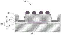
为解决上述技术问题,本申请提供一种硅基液晶芯片,请参阅图1,图1是本申请第一实施例中的硅基液晶芯片的侧面剖视图。如图1所示,本实施例中,硅基液晶芯片10包括:硅基液晶芯片10包括:玻璃盖板12、晶圆基板11、框胶13和液晶14。晶圆基板11上定义有管脚区111和切割区112。框胶13置于玻璃盖板12和晶圆基板11其中之一之上并形成有液晶空间(图未示),液晶14收容于液晶空间内,玻璃盖板12与晶圆基板11通过框胶13贴合,且框胶13覆盖晶圆基板11的管脚区111和切割区112。管脚区111相对切割区112更靠液晶14。管脚区上设置有液晶芯片10的输入输出端子(图未示)。In order to solve the above technical problems, the present application provides a liquid crystal on silicon chip, please refer to FIG. 1 , which is a side cross-sectional view of the liquid crystal on silicon chip in the first embodiment of the present application. As shown in FIG. 1 , in this embodiment, the liquid crystal on silicon chip 10 includes: the liquid crystal on silicon chip 10 includes: a
请参阅图2,图2是图1中的硅基液晶芯片的正面剖视图。在硅基液晶芯片10中,框胶13围设于液晶14之外,将液晶14限定在玻璃盖板12或晶圆基板11和框胶13之间形成的液晶空间内。Please refer to FIG. 2 . FIG. 2 is a front cross-sectional view of the liquid crystal on silicon chip in FIG. 1 . In the liquid crystal on silicon chip 10 , the
如图1所示,框胶13还覆盖晶圆基板11的管脚区111。如此,管脚区111和玻璃盖板12完全贴合,之间无空隙,在后续的工艺中,框胶13可以为管脚区111提供支撑避免管脚区111受损。换句话说,框胶13覆盖晶圆基板11的管脚区111可提高硅基液晶芯片10的生产良率。As shown in FIG. 1 , the
进一步地,液晶14与晶圆基板11和玻璃盖板12之间均无间隙。Further, there is no gap between the
如图1所示,液晶14和框胶13在晶圆基板11和玻璃盖板12之间,且可以充满晶圆基板11和玻璃盖板12之间的夹层,避免晶圆基板11和玻璃盖板12之间的液晶14所在的区域留有间隙,进而减少液晶14的流动,增加整体结构的可靠性。As shown in Figure 1, the
在一些具体的应用场景中,框胶13和液晶14涂覆在玻璃盖板12上,玻璃盖板12再和晶圆基板11贴合时,框胶13覆盖晶圆基板11的管脚区111和切割区112。In some specific application scenarios, the
在一些具体的应用场景中,框胶13和液晶14涂覆在晶圆基板11上,且框胶13覆盖管脚区111和切割区112,框胶13和晶圆基板11形成液晶空间,收容液晶14。In some specific application scenarios, the
进一步地,可以在玻璃盖板12上设置透明导电层(图未示),导电层具体可以为ITO。具体的,导电层设置在玻璃盖板12朝向晶圆基板11的面上。Further, a transparent conductive layer (not shown in the figure) may be provided on the
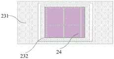
请参阅图3,图3是本申请第二实施例中的硅基液晶芯片的侧面剖视图。如图3所示,在硅基液晶芯片20中,框胶23包括间隔开的第一框胶231和第二框胶232,第二框胶232围绕液晶24,第一框胶231置于第二框胶232之外并围绕第二框胶232。Please refer to FIG. 3 . FIG. 3 is a side cross-sectional view of the liquid crystal on silicon chip in the second embodiment of the present application. As shown in FIG. 3, in the liquid crystal on
请参阅图4,图4是图3中的硅基液晶芯片的正面剖视图。在本实施例中,框胶23分为两部分,第二框胶232围绕形成收容液晶24的液晶空间,液晶空间可以固定液晶24在晶圆基板21和玻璃盖板22间的位置。第一框胶231与第二框胶232之间留有间隔,且第一框胶231可以完全覆盖晶圆基板21的管脚区211和切割区212,在管脚区211和玻璃盖板22间、切割区212和玻璃盖板22间起到支撑的作用,避免在芯片切割过程中导致的管脚区211受损,也可以减少芯片切割过程中芯片边角的崩裂、破损等。Please refer to FIG. 4 . FIG. 4 is a front cross-sectional view of the liquid crystal on silicon chip in FIG. 3 . In this embodiment, the
进一步地,第一框胶231和第二框胶232之间留有间隔,可以减小玻璃盖板22与晶圆基板21之间因材料差异而产生的应力,避免应力过大而导致芯片切割过程中芯片产生裂缝、或者应力过大导致芯片变形,减小应力对硅基液晶芯片20性能的影响,提高硅基液晶芯片20封装的可靠性。Further, there is a gap between the
另外,第一层框胶231还可以切割时防止硅基液晶芯片20切割时产生的硅碎屑以及水对管脚区造成污染。In addition, the first layer of
在本实施例中,晶圆基板21和玻璃盖板22的设置与第一实施例相同,此处不再赘述。进一步地,在本实施例中,晶圆基板21和玻璃盖板22之间的液晶24所在的区域被填满,液晶24与晶圆基板21以及玻璃盖板22之间均无间隙,确保液晶24在晶圆基板21和玻璃盖板22之间的位置保持稳定。In this embodiment, the arrangement of the
进一步地,与第一实施例相同,在本实施例中,第一框胶231和第二框胶232可以涂覆在玻璃盖板22上,并在玻璃盖板22和晶圆基板21贴合时第一框胶231覆盖管脚区211和切割区212。Further, same as the first embodiment, in this embodiment, the
与第一实施例相同,在本实施例中,第一框胶231和第二框胶232可以涂覆在晶圆基板21上,第一框胶231覆盖管脚区211和切割区212,且第二框胶232和晶圆基板21形成液晶空间。Same as the first embodiment, in this embodiment, the
在上述任一实施例中,在玻璃盖板和晶圆基板贴合面上的切割区对应的位置处设置指示标记,根据指示标记设置框胶和液晶的涂覆位置,以达到贴合玻璃盖板和晶圆基板时、框胶能够达到覆盖管脚区和切割区的效果。In any of the above embodiments, an indicator mark is set at the position corresponding to the cutting area on the bonding surface of the glass cover plate and the wafer substrate, and the coating position of the sealant and liquid crystal is set according to the indicator mark, so as to achieve the bonding of the glass cover When using boards and wafer substrates, the sealant can achieve the effect of covering the pin area and the cutting area.
在上述任一实施例中,晶圆基板远离玻璃盖板的一面铺设有线路并通过球状引脚栅格阵列封装。In any of the above-mentioned embodiments, the side of the wafer substrate away from the glass cover is laid with lines and packaged through a ball grid array.
球状引脚栅格阵列封装能够使得保证硅基液晶芯片的内存容量,且能够使得硅基液晶芯片具备更好的散热性能和电性能。The ball grid array package can ensure the memory capacity of the silicon-based liquid crystal chip, and can make the silicon-based liquid crystal chip have better heat dissipation performance and electrical performance.
进一步地,在其他得应用场景中,硅基晶片也可以采用其他的形式进行封装,例如集成电路封装(SOP)、薄小外形封装(TSOP)、系统级封装(SIP)等等,在不影响硅基液晶芯片性能的情况下,封装形式可以不做限制。Furthermore, in other application scenarios, silicon-based wafers can also be packaged in other forms, such as integrated circuit package (SOP), thin small outline package (TSOP), system-in-package (SIP), etc., without affecting In the case of the performance of the liquid crystal on silicon chip, the packaging form may not be limited.
进一步地,为解决上述技术问题,本申请提供一种硅基液晶芯片的封装方法,用于封装上述任一实施例中的硅基液晶芯片,即硅基液晶芯片包括玻璃盖板、晶圆基板、框胶和液晶。Further, in order to solve the above technical problems, the present application provides a packaging method for a silicon-based liquid crystal chip, which is used to package the silicon-based liquid crystal chip in any of the above embodiments, that is, the silicon-based liquid crystal chip includes a glass cover plate, a wafer substrate , frame glue and liquid crystal.
请参阅图5,图5是本申请硅基液晶芯片的封装方法的流程示意图。如图5所示,本申请硅基液晶芯片的封装方法具体包括如下步骤:Please refer to FIG. 5 . FIG. 5 is a schematic flow chart of the packaging method of the liquid crystal on silicon chip of the present application. As shown in Figure 5, the packaging method of the liquid crystal on silicon chip of the present application specifically includes the following steps:
S10:提供晶圆基板和玻璃盖板,晶圆基板上定义有管脚区和切割区。S10: Provide a wafer substrate and a glass cover, and a pin area and a cutting area are defined on the wafer substrate.
在本申请的硅基液晶芯片的封装方法中,硅基液晶芯片的封装需要提供晶圆基板和玻璃盖板。其中,将晶圆基板上的管脚与引线框架区域定义为管脚区,将晶圆基板上的切割区域定义为切割区。In the packaging method of the liquid crystal on silicon chip of the present application, the packaging of the liquid crystal on silicon chip needs to provide a wafer substrate and a glass cover. Wherein, the area of the pins and the lead frame on the wafer substrate is defined as the pin area, and the cutting area on the wafer substrate is defined as the cutting area.
S20:在晶圆基板上定义有管脚区的一面或玻璃盖板上设置框胶并形成液晶空间,以及在液晶空间内滴注液晶。S20: setting a sealant on the side of the wafer substrate defining pin areas or on the glass cover to form a liquid crystal space, and dripping liquid crystal into the liquid crystal space.
晶圆基板在经过光刻和离子可以定出pad位置并最后进行退火处理之后,将pad所在的晶圆基板的一面定义为晶圆基板定义有管脚区的一面。After the wafer substrate is subjected to photolithography and ionization to determine the pad position and finally annealed, the side of the wafer substrate where the pad is located is defined as the side of the wafer substrate defining the pin area.
其中,在晶圆基板定义有管脚区的一面或玻璃盖板上设置框胶之前,需先对晶圆基板进行清洗,例如进行离子(plasma)清洗和湿式清洗(wet clean),以去除晶圆基板表面的污染,提高晶圆基板表面的稳定性。Among them, before setting the sealant on the side of the wafer substrate defined with the pin area or on the glass cover, the wafer substrate needs to be cleaned first, such as ion (plasma) cleaning and wet cleaning (wet clean), to remove the crystal The pollution of the surface of the round substrate improves the stability of the surface of the wafer substrate.
具体地,框胶可以设置在玻璃盖板的表面上,也可以设置在干燥后的晶圆基板上定义有管脚区的一面上。在晶圆基板上定义有管脚区的一面设置框胶时,框胶能够覆盖管脚区和切割区;在玻璃盖板的表面设置框胶时,在玻璃盖板上对应于管脚区和切割区的位置处设置框胶。Specifically, the sealant can be disposed on the surface of the glass cover, or on the side of the dried wafer substrate that defines the pin region. When the sealant is set on the side of the wafer substrate where the pin area is defined, the sealant can cover the pin area and the cutting area; when the sealant is set on the surface of the glass cover, the corresponding pin area and cutting area on the glass cover Frame glue is set at the position of the cutting area.
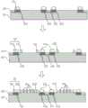
请参阅图6和图7,图6是本申请硅基液晶芯片的封装方法中步骤S20第一实施方式的制作流程示意图,图7是图6中的封装基板的正视图。Please refer to FIG. 6 and FIG. 7 , FIG. 6 is a schematic diagram of the manufacturing process of the first embodiment of step S20 in the packaging method of the liquid crystal on silicon chip of the present application, and FIG. 7 is a front view of the packaging substrate in FIG. 6 .
如图7所示,在本实施方式中,在晶圆基板103定义有管脚区1032的一面设置若干第一区域103a和置于第一区域103a之外并围绕每个第一区域103a的第二区域103b,第二区域103b覆盖晶圆基板103的管脚区1032和切割区1031。As shown in FIG. 7 , in this embodiment, a number of
其中,在每个第二区域103b内设置框胶102,框胶102围设第一区域103a形成液晶空间;并在所形成的液晶空间内滴注液晶。Wherein, a
在本实施方式中,第一区域103a即为液晶空间在晶圆基板103上的投影区域。具体地,在可以在每个第二区域103b内设置框胶102后,再在每个第一区域103a内滴注液晶104,以确保二者的相对滴注位置。In this embodiment, the
具体的,可以通过点胶或印刷涂布的方式在晶圆基板上或玻璃盖板上设置框胶并形成液晶空间,根据具体的pad尺寸调整印刷板的尺寸或者点胶方式,以控制框胶量。Specifically, the frame glue can be set on the wafer substrate or the glass cover plate by dispensing or printing coating to form a liquid crystal space, and the size of the printing plate or the glue dispensing method can be adjusted according to the specific pad size to control the frame glue. quantity.
在一实施方式中,如图6所示,可以通过点胶机101在晶圆基板103定义有管脚区1032的一面滴注框胶102。可以通过设置点胶机101的点胶程序,进而控制点胶机101在晶圆基板103的第二区域103b设置框胶102,框胶102设置完成后再在第一区域103a内滴注液晶104。In one embodiment, as shown in FIG. 6 , the
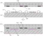
请参见图8,图8是本申请硅基液晶芯片的封装方法中步骤S20第二实施方式的制作流程示意图。在另一实施方式中,可以通过印刷板115在晶圆基板103上的每个第二区域103b内设置框胶,其框胶步骤包括:提供一印刷板115;其中,印刷板115对应第二区域103b的位置处设置有镂空116;将印刷板115罩设于晶圆基板103定义有管脚区1032的一面的上方并进行对位,对位后通过印刷板115上的镂空116往第二区域103b内填充框胶。Please refer to FIG. 8 . FIG. 8 is a schematic diagram of the manufacturing process of the second embodiment of step S20 in the packaging method of the liquid crystal on silicon chip of the present application. In another embodiment, a sealant can be provided in each
在本实施方式中,通过印刷板115在晶圆基板113上的每个第二区域113b内设置框胶112,包括:提供一印刷板115;其中,印刷板115对应第二区域113b的位置处设置有镂空116;将印刷板115罩设于晶圆基板113定义有管脚区的一面的上方并进行对位,对位后通过印刷板115上的镂空116往第二区域113b内填充框胶112。In this embodiment, setting the
具体的,在印刷时,将印刷板115罩设于晶圆基板113定义有管脚区的一面的上方并进行对位,对位后通过印刷板115上的镂空116往第二区域113b内填充框胶112,将胶体铺设在印刷板115上,并用刮板推动胶体在印刷板115上运动,胶体会通过印刷板115上的镂空116往第二区域113b内流动。通过印刷板115上设置的镂空116的位置,可以控制框胶112在晶圆基板113定义有管脚区的一面的填充位置。具体的印刷过程可以通过人工完成,也可以选择其他印刷方式,此处不做限制。Specifically, during printing, the printed
框胶112填充完成后,取下印刷板115,在框胶112所围设的液晶空间也即第二区域113b内滴注液晶114。After the
进一步地,还可以选择在玻璃盖板上设置框胶112和滴注液晶114。具体的,在玻璃盖板与晶圆基板113的管脚区和切割区相对应的位置处设置框胶112,并在框胶112围封的液晶空间内滴注液晶114。Further, a
请参阅图9和图10,图9是本申请硅基液晶芯片的封装方法中步骤S20第三实施方式的制作流程示意图,图10是图9中的玻璃盖板的正视图。Please refer to FIG. 9 and FIG. 10 , FIG. 9 is a schematic diagram of the manufacturing process of the third embodiment of step S20 in the packaging method of the liquid crystal on silicon chip of the present application, and FIG. 10 is a front view of the glass cover in FIG. 9 .
在本实施方式中,晶圆基板上(图未示)定义有管脚区的一面设置若干第一区域(图未示)和围绕每个第一区域的第二区域(图未示),第二区域包括晶圆基板的管脚区和切割区,第一区域和第二区域在晶圆基板上的设置位置与上述任一实施方式中相同,此处不再赘述。In this embodiment, several first regions (not shown) and second regions (not shown) surrounding each first region are provided on the side of the wafer substrate (not shown) that defines the pin area. The second area includes the pin area and the cutting area of the wafer substrate, and the positions of the first area and the second area on the wafer substrate are the same as those in any of the above embodiments, and will not be repeated here.
在本实施方式中,将玻璃盖板126朝向晶圆基板设置有框胶122的一面定义为第一表面。如图10所示,在本实施方式中,在晶圆基板的切割区(图未示)设置第一标记(图未示),在玻璃盖板126的第一表面上设置与晶圆基板贴合对位用的第二标记1261,且第二标记1261与第一标记在玻璃盖板126与晶圆基板贴合后一一对应。In this embodiment, the side of the
如图9所示,在本实施方式中,玻璃盖板126和晶圆基板之间的框胶122的设置过程和液晶124的滴注过程是在玻璃盖板126的第一表面进行。具体地,在玻璃盖板126的表面上或晶圆基板上设置框胶122和滴注液晶124,且框胶122覆盖第二区域;再通过第一标记和第二标记1261对位贴合玻璃盖板126和晶圆基板。As shown in FIG. 9 , in this embodiment, the setting process of the
在一些具体的封装场景中,可以先在第二区域内设置框胶122,再在框胶122所围设的液晶空间内滴注液晶124。框胶122的设置过程可以与第一实施方式、第二实施方式中相同,此处不做限制。In some specific packaging scenarios, the
进一步地,框胶122包括第一框胶和第二框胶。第二框胶用于形成液晶空间并围封液晶124,第一框胶环绕于第二框胶之外并覆盖管脚区和切割区。进一步地,玻璃盖板126对应管脚区和切割区设置有第二框胶,玻璃盖板126在第二框胶之内设置有用于围封液晶124并形成液晶空间的第一框胶。Further, the
请参阅图11和图12,图11是本申请硅基液晶芯片的封装方法中步骤S20第四实施方式的制作流程示意图,图12是图11中的晶圆基板的正视图。Please refer to FIG. 11 and FIG. 12 , FIG. 11 is a schematic diagram of the manufacturing process of the fourth embodiment of step S20 in the packaging method of the liquid crystal on silicon chip of the present application, and FIG. 12 is a front view of the wafer substrate in FIG. 11 .
在本实施方式中,第一区域133a和第二区域133b的设置与上述实施方式中相同,此处不再赘述。如图11和图12所示,在本实施方式中,框胶132包括第一框胶1321和第二框胶1322,第二区域133b包括间隔开的第三区域1331b和第四区域1332b,第四区域1332b围绕第一区域133a,第三区域1331b置于第四区域1332b之外并围绕所述第四区域1332b,且第三区域1331b内定义有管脚区1332和切割区1331。In this embodiment, the settings of the
如图11所示,在本实施方式中,在晶圆基板133上定义有管脚区1332的一面设置框胶132,包括:提供印刷板(图未示),印刷板遮盖对应晶圆基板133的第三区域1331b(详见图12)和第四区域1332b(详见图12)的位置处设置有镂空;将印刷板罩设于晶圆基板133定义有管脚区1332的一面的上方并进行对位,对位后通过印刷版上的镂空往第三区域1331b内填充第一框胶1321,往第四区域内1332b填充第二框胶1322。As shown in FIG. 11 , in this embodiment, the
具体的滴注方法可以与第二实施方式相同,此处不再赘述。The specific instillation method may be the same as that in the second embodiment, and will not be repeated here.
第一框胶1321和第二框胶1322填充完成后,可以取下印刷板,并在第二框胶1322所围设的液晶空间内滴注液晶134。其中,第一框胶1321和第二框胶1322的填充过程可以通过点胶或者印刷的方式完成,此处不做限制。After filling the
进一步地,请参阅图13,图13是本申请硅基液晶芯片的封装方法中步骤S20第五实施方式的制作流程示意图。Further, please refer to FIG. 13 . FIG. 13 is a schematic diagram of the manufacturing process of the fifth embodiment of step S20 in the packaging method of the liquid crystal on silicon chip of the present application.
如图13所示,在本实施方式中,框胶142包括第一框胶1421和第二框胶1422,在玻璃盖板146的第一表面设置框胶142和滴注液晶144,具体过程可以包括:在每个第二标记1461的每侧由近及远依次滴注第一框胶1421、第二框胶1422和液晶144。As shown in FIG. 13 , in this embodiment, the
具体地,在本实施方式中,第二标记1461的设置可以与第三实施方式中相同,此处不再赘述。其中,框胶142和液晶144的滴注可以通过人工点胶完成,也可以与第一实施方式、第二实施方式中的任一个相同,此处不做限制。Specifically, in this embodiment, the setting of the
进一步地,在本实施方式中,第一框胶1421覆盖第二区域,第一框胶1421的滴注区域围绕第二框胶1422的滴注区域并与第二框胶1422的滴注区域间隔设置,第二框胶1422的滴注区域围绕液晶144的滴注区域并与液晶144的滴注区域相邻设置。Further, in this embodiment, the
与第三实施方式不同的是,本实施方式中,框胶142包括间隔设置的第一框胶1421和第二框胶1422,第二框胶1422围绕液晶144设置,可以避免液晶144的滴注位置的偏移,而第一框胶1421和第二框胶1422间隔设置,可以减小玻璃盖板146和晶圆基板(图未示)之间的应力,提高整个封装结构的可靠性。The difference from the third embodiment is that in this embodiment, the
进一步地,在上述任一实施方式中,可以在玻璃盖板上设置透明导电层(图未示),导电层具体可以为ITO。Further, in any of the above implementation manners, a transparent conductive layer (not shown in the figure) may be provided on the glass cover plate, and the conductive layer may specifically be ITO.
S30:通过框胶贴合晶圆基板定义有管脚区的一面和玻璃盖板,框胶在晶圆基板与玻璃盖板贴合后覆盖晶圆基板的管脚区和切割区。S30: Bonding the side of the wafer substrate defining the pin area and the glass cover with a frame glue, the frame glue covers the pin area and the cutting area of the wafer substrate after the wafer substrate and the glass cover are bonded.
具体地,框胶和液晶滴注时为水滴状,晶圆基板定义有管脚区的一面和玻璃盖板挤压之后框胶和液晶可以平铺在晶圆基板和玻璃盖板之间,形成阵列排布的液晶空间区和框胶空间区。Specifically, the frame glue and liquid crystal are in the shape of water droplets when they are dripped. After the side of the wafer substrate defining the pin area and the glass cover are squeezed, the frame glue and liquid crystal can be spread flat between the wafer substrate and the glass cover to form The liquid crystal space area and the frame glue space area arranged in an array.
具体地,设置框胶的点胶量和点胶位置使得框胶平铺后可以覆盖晶圆基板的管脚区和切割区,晶圆基板的管脚区和切割区未被液晶覆盖,如果没有框胶覆盖,晶圆基板的管脚区和切割区与玻璃盖板间会出现悬空间隙。Specifically, set the dispensing amount and dispensing position of the frame glue so that the frame glue can cover the pin area and the cutting area of the wafer substrate after being tiled. The pin area and the cutting area of the wafer substrate are not covered by the liquid crystal. If there is no Covered by the frame glue, there will be a floating gap between the pin area and the cutting area of the wafer substrate and the glass cover.
具体地,在步骤S20的第一实施方式、第二实施方式和第四实施方式的应用场景中,可以直接贴合玻璃盖板的第一表面和晶圆基板上定义有管脚区的一面,以贴合玻璃盖板和晶圆基板。Specifically, in the application scenarios of the first embodiment, the second embodiment, and the fourth embodiment of step S20, the first surface of the glass cover and the side of the wafer substrate defining the pin region can be directly attached, To bond glass cover and wafer substrate.
请参阅图14,图14是本申请硅基液晶芯片的封装方法中步骤S30第一实施方式的制作流程示意图,具体对应于步骤S20的第一实施方式和第二实施方式之后的步骤。晶圆基板202定义有管脚区2022的一面设置框胶203并滴注有液晶204,玻璃盖板201的第一表面朝向晶圆基板202定义有管脚区2022的一面贴合。二者贴合后框胶203可以覆盖晶圆基板202的管脚区2022和切割区2021,避免管脚区2022和切割区2021与玻璃盖板201的第一表面之间出现悬空。Please refer to FIG. 14 . FIG. 14 is a schematic diagram of the production process of the first embodiment of step S30 in the packaging method of the liquid crystal on silicon chip of the present application, which specifically corresponds to the steps after the first embodiment and the second embodiment of step S20 . The side of the
进一步地,请参阅图15,图15是本申请硅基液晶芯片的封装方法中步骤S30第二实施方式的制作流程示意图,具体对应于步骤S20的第三实施方式之后的步骤。Further, please refer to FIG. 15 . FIG. 15 is a schematic diagram of the production process of the second embodiment of step S30 in the packaging method of the liquid crystal on silicon chip of the present application, which specifically corresponds to the steps after the third embodiment of step S20 .
如图15所示,晶圆基板212定义有管脚区的一面朝向玻璃盖板216的第一表面贴合,具体为通过晶圆基板212定义有管脚区的一面的第一标记2123与玻璃盖板216的第一表面上的第二标记2161对位贴合。其中玻璃盖板216的第一表面设置有框胶213并滴注有液晶214,框胶213覆盖第二区域,使得贴合后框胶213可以覆盖晶圆基板212的管脚区2122和切割区2121。As shown in FIG. 15 , the side of the
进一步地,请参阅图16,图16是本申请硅基液晶芯片的封装方法中步骤S30第三实施方式的制作流程示意图,具体对应于步骤S20的第四实施方式之后的步骤。Further, please refer to FIG. 16 . FIG. 16 is a schematic diagram of the manufacturing process of the third embodiment of step S30 in the packaging method of the liquid crystal on silicon chip of the present application, which specifically corresponds to the steps after the fourth embodiment of step S20 .
本实施方式中玻璃盖板221的第一表面朝向晶圆基板222定义有管脚区2222的一面贴合,其中,晶圆基板222定义有管脚区2222的一面设置有框胶223并滴注有液晶224,框胶223包括第一框胶2231和第二框胶2232。玻璃盖板221和晶圆基板222贴合后,第一框胶2231可以覆盖晶圆基板222的管脚区2222和切割区2221,同时第二框胶2232与液晶224相邻,与第一框胶2231间隔,可以减小玻璃盖板221和晶圆基板222之间的应力。In this embodiment, the first surface of the
进一步地,请参阅图17,图17是本申请硅基液晶芯片的封装方法中步骤S30第四实施方式的制作流程示意图,具体对应于步骤S20的第五实施方式之后的步骤。Further, please refer to FIG. 17 . FIG. 17 is a schematic diagram of the manufacturing process of the fourth embodiment of step S30 in the packaging method of the liquid crystal on silicon chip of the present application, which specifically corresponds to the steps after the fifth embodiment of step S20 .
在本实施方式中,晶圆基板235和玻璃盖板236的贴合也是通过第一标记2353与第二标记2361的对位贴合实现的,此处不再赘述。In this embodiment, the lamination of the
在本实施方式中,框胶233包括第一框胶2331和第二框胶2332。晶圆基板235与玻璃盖板236对位贴合后,第一框胶2331覆盖晶圆基板235的管脚区2352和切割区2351,且第二框胶2332与液晶234相邻,与第一框胶2331间隔设置,能够减小晶圆基板235与玻璃盖板236之间的应力。In this embodiment, the
具体地,玻璃盖板236和晶圆基板235贴合后,可以对框胶233进行固化。固化后的框胶233可以固定连接晶圆基板235和玻璃盖板236,以确保硅基液晶芯片的封装基板的密封性能,同时对液晶234的铺设区域进行围设限制。Specifically, after the
S40:沿切割区对晶圆基板和玻璃盖板进行切割,得到硅基液晶芯片。S40: cutting the wafer substrate and the glass cover plate along the cutting area to obtain a silicon-based liquid crystal chip.
框胶固化完成之后,晶圆基板与玻璃盖板之间密封固定,可以沿封装基板的厚度方向通过切割区对封装基板进行切割,以分离出各个硅基液晶芯片。其中,在晶圆基板为采用晶片级封装方法(WLP)封装的晶圆的应用场景中,可以通过切割区直接对硅基液晶芯片的封装基板进行切割。在晶圆基板为采用未封装的硅基晶圆的应用场景中,在沿封装基板的厚度方向在切割区切割封装基板之前具体需要先执行以下步骤。After the sealant is cured, the wafer substrate and the glass cover are sealed and fixed, and the packaging substrate can be cut along the thickness direction of the packaging substrate through the cutting area to separate individual liquid crystal on silicon chips. Wherein, in an application scenario where the wafer substrate is a wafer packaged by wafer level packaging (WLP), the packaging substrate of the liquid crystal on silicon chip can be directly cut through the cutting area. In the application scenario where the wafer substrate is an unpackaged silicon-based wafer, the following steps need to be performed before cutting the packaging substrate in the cutting area along the thickness direction of the packaging substrate.
步骤一:通过研磨晶圆基板背离定义有管脚区的一面将晶圆基板减薄至预设厚度。Step 1: Thinning the wafer substrate to a preset thickness by grinding the side of the wafer substrate facing away from the pin area defined.
步骤二:在晶圆基板背离定义有管脚区的一面通过硅通孔技术开孔以显露管脚区。Step 2: opening holes on the side of the wafer substrate away from the defined pin area to expose the pin area through silicon via technology.
步骤三:在晶圆基板背离定义有管脚区的一面铺设线路并进行球状引脚栅格阵列封装。Step 3: Laying lines on the side of the wafer substrate away from the defined pin area and performing ball grid array packaging.
上述步骤完成之后,便可以通过切割区域切割硅基液晶芯片的封装基板以分离出对应的各个硅基液晶芯片。After the above steps are completed, the encapsulation substrate of the liquid crystal on silicon chip can be cut through the cutting area to separate corresponding liquid crystal on silicon chips.
综上所述,本申请通过在液晶芯片封装时在芯片的管脚区和切割区涂覆上框胶,对芯片的管脚区和切割区起到支撑保护的目的,一方面避免管脚区处于一种悬浮的状态,进而易被外界产生的震动或者应力的作用损坏,同时可以将切割区保护起来,避免在通过切割区切割硅基液晶芯片的封装基板时在硅基液晶芯片的切割区位置产生较多的碎屑和破损;进一步地,本申请还设置框胶包括间隔设置的第一框胶和第二框胶,第一框胶覆盖切割区和管脚区,第二框胶围绕液晶设置,在保护管脚区和芯片切割过程的同时,减少玻璃盖板与晶圆基板之间的应力,提高芯片封装过程的可靠性。To sum up, this application provides support and protection for the pin area and cutting area of the chip by coating the frame glue on the pin area and cutting area of the chip when the liquid crystal chip is packaged. In a state of suspension, it is easy to be damaged by vibration or stress generated by the outside world. At the same time, the cutting area can be protected to avoid the cutting area of the silicon-based liquid crystal chip when cutting the packaging substrate of the silicon-based liquid crystal chip through the cutting area. More debris and damage are generated at the position; further, the application also sets the frame glue to include the first frame glue and the second frame glue arranged at intervals, the first frame glue covers the cutting area and the pin area, and the second frame glue surrounds the The liquid crystal setting, while protecting the pin area and the chip cutting process, reduces the stress between the glass cover and the wafer substrate, and improves the reliability of the chip packaging process.
以上所述仅为本申请的实施方式,并非因此限制本申请的专利范围,凡是利用本申请说明书及附图内容所作的等效结构或等效流程变换,或直接或间接运用在其他相关的技术领域,均同理包括在本申请的专利保护范围内。The above is only the implementation of the application, and does not limit the patent scope of the application. Any equivalent structure or equivalent process conversion made by using the specification and drawings of the application, or directly or indirectly used in other related technologies fields, are all included in the scope of patent protection of this application in the same way.
Claims (13)
Priority Applications (1)
| Application Number | Priority Date | Filing Date | Title |
|---|---|---|---|
| CN202111547515.XACN116266020A (en) | 2021-12-16 | 2021-12-16 | Packaging method of silicon-based liquid crystal chip and chip |
Applications Claiming Priority (1)
| Application Number | Priority Date | Filing Date | Title |
|---|---|---|---|
| CN202111547515.XACN116266020A (en) | 2021-12-16 | 2021-12-16 | Packaging method of silicon-based liquid crystal chip and chip |
Publications (1)
| Publication Number | Publication Date |
|---|---|
| CN116266020Atrue CN116266020A (en) | 2023-06-20 |
Family
ID=86742792
Family Applications (1)
| Application Number | Title | Priority Date | Filing Date |
|---|---|---|---|
| CN202111547515.XAPendingCN116266020A (en) | 2021-12-16 | 2021-12-16 | Packaging method of silicon-based liquid crystal chip and chip |
Country Status (1)
| Country | Link |
|---|---|
| CN (1) | CN116266020A (en) |
Citations (16)
| Publication number | Priority date | Publication date | Assignee | Title |
|---|---|---|---|---|
| KR20030043518A (en)* | 2001-11-28 | 2003-06-02 | 삼성에스디아이 주식회사 | Liquid crystal display package and manufacturing method of the same |
| US20030214618A1 (en)* | 2002-05-17 | 2003-11-20 | Advanced Semiconductor Engineering, Inc. | Liquid crystal display device with bump and method for manufacturing the same |
| KR20030092607A (en)* | 2002-05-30 | 2003-12-06 | 삼성에스디아이 주식회사 | Liquid crystal display package and manufacturing method of the same |
| JP2005091723A (en)* | 2003-09-17 | 2005-04-07 | Seiko Epson Corp | Manufacturing method of liquid crystal display device, substrate for liquid crystal display device and liquid crystal display device |
| CN1607437A (en)* | 2003-10-16 | 2005-04-20 | 鸿富锦精密工业(深圳)有限公司 | Liquid crystal panel manufacturing method |
| US20060023155A1 (en)* | 2004-07-30 | 2006-02-02 | Magana John F | Wafer scale fabrication of liquid crystal on silicon light modulation devices |
| US20060082716A1 (en)* | 2002-12-20 | 2006-04-20 | Hugues Lebrun | Method of producing liquid crystal cells on a silicon substrate and corresponding cells |
| CN201133992Y (en)* | 2007-12-29 | 2008-10-15 | 上海广电光电子有限公司 | LCD device |
| US20090273005A1 (en)* | 2006-07-24 | 2009-11-05 | Hung-Yi Lin | Opto-electronic package structure having silicon-substrate and method of forming the same |
| US20130032944A1 (en)* | 2011-08-01 | 2013-02-07 | Tessera, Inc. | Microelectronic package with stacked microelectronic elements and method for manufacture thereof |
| CN104849893A (en)* | 2014-02-19 | 2015-08-19 | 美商晶典有限公司 | Silicon-based liquid crystal wafer grade liquid crystal assembly, display module and manufacturing method for same |
| CN108364981A (en)* | 2018-01-31 | 2018-08-03 | 昆山国显光电有限公司 | A kind of cutting method of display panel, sub- display panel and display panel |
| CN108828820A (en)* | 2018-06-27 | 2018-11-16 | 豪威半导体(上海)有限责任公司 | LCoS display panel and its manufacturing method |
| US20190086708A1 (en)* | 2017-09-18 | 2019-03-21 | Omnivision Technologies, Inc. | Liquid crystal on silicon packaging |
| CN213659133U (en)* | 2020-11-17 | 2021-07-09 | 蔡明伟 | Optical chip packaging structure |
| CN217112992U (en)* | 2021-12-16 | 2022-08-02 | 深圳晶微峰光电科技有限公司 | Silicon-based liquid crystal chip |
- 2021
- 2021-12-16CNCN202111547515.XApatent/CN116266020A/enactivePending
Patent Citations (16)
| Publication number | Priority date | Publication date | Assignee | Title |
|---|---|---|---|---|
| KR20030043518A (en)* | 2001-11-28 | 2003-06-02 | 삼성에스디아이 주식회사 | Liquid crystal display package and manufacturing method of the same |
| US20030214618A1 (en)* | 2002-05-17 | 2003-11-20 | Advanced Semiconductor Engineering, Inc. | Liquid crystal display device with bump and method for manufacturing the same |
| KR20030092607A (en)* | 2002-05-30 | 2003-12-06 | 삼성에스디아이 주식회사 | Liquid crystal display package and manufacturing method of the same |
| US20060082716A1 (en)* | 2002-12-20 | 2006-04-20 | Hugues Lebrun | Method of producing liquid crystal cells on a silicon substrate and corresponding cells |
| JP2005091723A (en)* | 2003-09-17 | 2005-04-07 | Seiko Epson Corp | Manufacturing method of liquid crystal display device, substrate for liquid crystal display device and liquid crystal display device |
| CN1607437A (en)* | 2003-10-16 | 2005-04-20 | 鸿富锦精密工业(深圳)有限公司 | Liquid crystal panel manufacturing method |
| US20060023155A1 (en)* | 2004-07-30 | 2006-02-02 | Magana John F | Wafer scale fabrication of liquid crystal on silicon light modulation devices |
| US20090273005A1 (en)* | 2006-07-24 | 2009-11-05 | Hung-Yi Lin | Opto-electronic package structure having silicon-substrate and method of forming the same |
| CN201133992Y (en)* | 2007-12-29 | 2008-10-15 | 上海广电光电子有限公司 | LCD device |
| US20130032944A1 (en)* | 2011-08-01 | 2013-02-07 | Tessera, Inc. | Microelectronic package with stacked microelectronic elements and method for manufacture thereof |
| CN104849893A (en)* | 2014-02-19 | 2015-08-19 | 美商晶典有限公司 | Silicon-based liquid crystal wafer grade liquid crystal assembly, display module and manufacturing method for same |
| US20190086708A1 (en)* | 2017-09-18 | 2019-03-21 | Omnivision Technologies, Inc. | Liquid crystal on silicon packaging |
| CN108364981A (en)* | 2018-01-31 | 2018-08-03 | 昆山国显光电有限公司 | A kind of cutting method of display panel, sub- display panel and display panel |
| CN108828820A (en)* | 2018-06-27 | 2018-11-16 | 豪威半导体(上海)有限责任公司 | LCoS display panel and its manufacturing method |
| CN213659133U (en)* | 2020-11-17 | 2021-07-09 | 蔡明伟 | Optical chip packaging structure |
| CN217112992U (en)* | 2021-12-16 | 2022-08-02 | 深圳晶微峰光电科技有限公司 | Silicon-based liquid crystal chip |
Similar Documents
| Publication | Publication Date | Title |
|---|---|---|
| TWI796522B (en) | Semiconductor device packaging method and semiconductor device | |
| JP4757398B2 (en) | Manufacturing method of semiconductor device | |
| TWI239655B (en) | Photosensitive semiconductor package with support member and method for fabricating the same | |
| TWI508245B (en) | Package of embedded chip and manufacturing method thereof | |
| TWI414027B (en) | Chip-sized package and fabrication method thereof | |
| CN105762084B (en) | Packaging method and packaging device of flip chip | |
| TW201101398A (en) | Package process and package structure | |
| CN101740551A (en) | Laminated crystal grain packaging structure for semiconductor element and method thereof | |
| CN101477955B (en) | Small chip reconfiguration packaging structure and packaging method | |
| CN101477956B (en) | Small chip reconfiguration packaging structure and packaging method | |
| TWI245350B (en) | Wafer level semiconductor package with build-up layer | |
| TWI303870B (en) | Structure and mtehod for packaging a chip | |
| TWI236747B (en) | Manufacturing process and structure for a flip-chip package | |
| TWM455258U (en) | Image sensor structure with air gap | |
| TWI421956B (en) | Chip-sized package and fabrication method thereof | |
| TWI245430B (en) | Fabrication method of semiconductor package with photosensitive chip | |
| CN100413044C (en) | Glue filling structure for wafer-level chip size packaging and method thereof | |
| JP2002368028A (en) | Semiconductor package and manufacturing method thereof | |
| CN116154048A (en) | Method for preparing LED device based on surface patch | |
| TW201705316A (en) | Chip packaging process and chip package | |
| TW200849503A (en) | Package-on-package structure and method for making the same | |
| TW201405673A (en) | Method of forming chip scale package | |
| CN113380729A (en) | Fan-out type packaging method and fan-out type packaging device | |
| CN116266020A (en) | Packaging method of silicon-based liquid crystal chip and chip | |
| CN100590823C (en) | Method for manufacturing alignment mark used in packaging structure with reconfigured crystal grains |
Legal Events
| Date | Code | Title | Description |
|---|---|---|---|
| PB01 | Publication | ||
| PB01 | Publication | ||
| SE01 | Entry into force of request for substantive examination | ||
| SE01 | Entry into force of request for substantive examination |