CN116250091A - LED device and method of manufacturing LED device - Google Patents
LED device and method of manufacturing LED deviceDownload PDFInfo
- Publication number
- CN116250091A CN116250091ACN202180067709.1ACN202180067709ACN116250091ACN 116250091 ACN116250091 ACN 116250091ACN 202180067709 ACN202180067709 ACN 202180067709ACN 116250091 ACN116250091 ACN 116250091A
- Authority
- CN
- China
- Prior art keywords
- led
- layer
- region
- emitting region
- porous
- Prior art date
- Legal status (The legal status is an assumption and is not a legal conclusion. Google has not performed a legal analysis and makes no representation as to the accuracy of the status listed.)
- Pending
Links
Images


Classifications
- H—ELECTRICITY
- H10—SEMICONDUCTOR DEVICES; ELECTRIC SOLID-STATE DEVICES NOT OTHERWISE PROVIDED FOR
- H10H—INORGANIC LIGHT-EMITTING SEMICONDUCTOR DEVICES HAVING POTENTIAL BARRIERS
- H10H20/00—Individual inorganic light-emitting semiconductor devices having potential barriers, e.g. light-emitting diodes [LED]
- H10H20/80—Constructional details
- H10H20/81—Bodies
- H10H20/817—Bodies characterised by the crystal structures or orientations, e.g. polycrystalline, amorphous or porous
- H10H20/818—Bodies characterised by the crystal structures or orientations, e.g. polycrystalline, amorphous or porous within the light-emitting regions
- H—ELECTRICITY
- H10—SEMICONDUCTOR DEVICES; ELECTRIC SOLID-STATE DEVICES NOT OTHERWISE PROVIDED FOR
- H10H—INORGANIC LIGHT-EMITTING SEMICONDUCTOR DEVICES HAVING POTENTIAL BARRIERS
- H10H20/00—Individual inorganic light-emitting semiconductor devices having potential barriers, e.g. light-emitting diodes [LED]
- H10H20/80—Constructional details
- H10H20/81—Bodies
- H10H20/822—Materials of the light-emitting regions
- H10H20/824—Materials of the light-emitting regions comprising only Group III-V materials, e.g. GaP
- H10H20/825—Materials of the light-emitting regions comprising only Group III-V materials, e.g. GaP containing nitrogen, e.g. GaN
- H—ELECTRICITY
- H10—SEMICONDUCTOR DEVICES; ELECTRIC SOLID-STATE DEVICES NOT OTHERWISE PROVIDED FOR
- H10H—INORGANIC LIGHT-EMITTING SEMICONDUCTOR DEVICES HAVING POTENTIAL BARRIERS
- H10H20/00—Individual inorganic light-emitting semiconductor devices having potential barriers, e.g. light-emitting diodes [LED]
- H10H20/01—Manufacture or treatment
- H10H20/011—Manufacture or treatment of bodies, e.g. forming semiconductor layers
- H10H20/013—Manufacture or treatment of bodies, e.g. forming semiconductor layers having light-emitting regions comprising only Group III-V materials
- H10H20/0133—Manufacture or treatment of bodies, e.g. forming semiconductor layers having light-emitting regions comprising only Group III-V materials with a substrate not being Group III-V materials
- H10H20/01335—Manufacture or treatment of bodies, e.g. forming semiconductor layers having light-emitting regions comprising only Group III-V materials with a substrate not being Group III-V materials the light-emitting regions comprising nitride materials
- H—ELECTRICITY
- H10—SEMICONDUCTOR DEVICES; ELECTRIC SOLID-STATE DEVICES NOT OTHERWISE PROVIDED FOR
- H10H—INORGANIC LIGHT-EMITTING SEMICONDUCTOR DEVICES HAVING POTENTIAL BARRIERS
- H10H20/00—Individual inorganic light-emitting semiconductor devices having potential barriers, e.g. light-emitting diodes [LED]
- H10H20/01—Manufacture or treatment
- H10H20/011—Manufacture or treatment of bodies, e.g. forming semiconductor layers
- H10H20/013—Manufacture or treatment of bodies, e.g. forming semiconductor layers having light-emitting regions comprising only Group III-V materials
- H10H20/0137—Manufacture or treatment of bodies, e.g. forming semiconductor layers having light-emitting regions comprising only Group III-V materials the light-emitting regions comprising nitride materials
- H—ELECTRICITY
- H10—SEMICONDUCTOR DEVICES; ELECTRIC SOLID-STATE DEVICES NOT OTHERWISE PROVIDED FOR
- H10H—INORGANIC LIGHT-EMITTING SEMICONDUCTOR DEVICES HAVING POTENTIAL BARRIERS
- H10H20/00—Individual inorganic light-emitting semiconductor devices having potential barriers, e.g. light-emitting diodes [LED]
- H10H20/80—Constructional details
- H10H20/81—Bodies
- H10H20/811—Bodies having quantum effect structures or superlattices, e.g. tunnel junctions
- H10H20/812—Bodies having quantum effect structures or superlattices, e.g. tunnel junctions within the light-emitting regions, e.g. having quantum confinement structures
- H—ELECTRICITY
- H10—SEMICONDUCTOR DEVICES; ELECTRIC SOLID-STATE DEVICES NOT OTHERWISE PROVIDED FOR
- H10H—INORGANIC LIGHT-EMITTING SEMICONDUCTOR DEVICES HAVING POTENTIAL BARRIERS
- H10H20/00—Individual inorganic light-emitting semiconductor devices having potential barriers, e.g. light-emitting diodes [LED]
- H10H20/80—Constructional details
- H10H20/81—Bodies
- H10H20/813—Bodies having a plurality of light-emitting regions, e.g. multi-junction LEDs or light-emitting devices having photoluminescent regions within the bodies
- H—ELECTRICITY
- H10—SEMICONDUCTOR DEVICES; ELECTRIC SOLID-STATE DEVICES NOT OTHERWISE PROVIDED FOR
- H10H—INORGANIC LIGHT-EMITTING SEMICONDUCTOR DEVICES HAVING POTENTIAL BARRIERS
- H10H20/00—Individual inorganic light-emitting semiconductor devices having potential barriers, e.g. light-emitting diodes [LED]
- H10H20/80—Constructional details
- H10H20/81—Bodies
- H10H20/817—Bodies characterised by the crystal structures or orientations, e.g. polycrystalline, amorphous or porous
- H—ELECTRICITY
- H10—SEMICONDUCTOR DEVICES; ELECTRIC SOLID-STATE DEVICES NOT OTHERWISE PROVIDED FOR
- H10H—INORGANIC LIGHT-EMITTING SEMICONDUCTOR DEVICES HAVING POTENTIAL BARRIERS
- H10H20/00—Individual inorganic light-emitting semiconductor devices having potential barriers, e.g. light-emitting diodes [LED]
- H10H20/80—Constructional details
- H10H20/84—Coatings, e.g. passivation layers or antireflective coatings
- H10H20/841—Reflective coatings, e.g. dielectric Bragg reflectors
- H—ELECTRICITY
- H10—SEMICONDUCTOR DEVICES; ELECTRIC SOLID-STATE DEVICES NOT OTHERWISE PROVIDED FOR
- H10H—INORGANIC LIGHT-EMITTING SEMICONDUCTOR DEVICES HAVING POTENTIAL BARRIERS
- H10H29/00—Integrated devices, or assemblies of multiple devices, comprising at least one light-emitting semiconductor element covered by group H10H20/00
- H10H29/01—Manufacture or treatment
- H10H29/012—Manufacture or treatment of active-matrix LED displays
- H—ELECTRICITY
- H10—SEMICONDUCTOR DEVICES; ELECTRIC SOLID-STATE DEVICES NOT OTHERWISE PROVIDED FOR
- H10H—INORGANIC LIGHT-EMITTING SEMICONDUCTOR DEVICES HAVING POTENTIAL BARRIERS
- H10H29/00—Integrated devices, or assemblies of multiple devices, comprising at least one light-emitting semiconductor element covered by group H10H20/00
- H10H29/10—Integrated devices comprising at least one light-emitting semiconductor component covered by group H10H20/00
- H10H29/14—Integrated devices comprising at least one light-emitting semiconductor component covered by group H10H20/00 comprising multiple light-emitting semiconductor components
- H10H29/142—Two-dimensional arrangements, e.g. asymmetric LED layout
- H—ELECTRICITY
- H10—SEMICONDUCTOR DEVICES; ELECTRIC SOLID-STATE DEVICES NOT OTHERWISE PROVIDED FOR
- H10H—INORGANIC LIGHT-EMITTING SEMICONDUCTOR DEVICES HAVING POTENTIAL BARRIERS
- H10H29/00—Integrated devices, or assemblies of multiple devices, comprising at least one light-emitting semiconductor element covered by group H10H20/00
- H10H29/30—Active-matrix LED displays
Landscapes
- Led Devices (AREA)
Abstract
Description
Translated fromChinese技术领域technical field
本发明涉及发光二极管(LED)及制造LED的改良方法。The present invention relates to light emitting diodes (LEDs) and improved methods of making LEDs.
背景技术Background technique
III-V族半导体材料受到半导体装置设计的特别关注,特别是III族-氮化物半导体材料的家族。Group III-V semiconductor materials are of particular interest in semiconductor device design, particularly the family of Group III-nitride semiconductor materials.
“III-V族”半导体包括如Ga、Al及In的III族元素及如N、P、As及Sb的V族元素的二元、三元及四元合金,且受到包括光电子学的多种应用的大量关注。"III-V" semiconductors include binary, ternary, and quaternary alloys of Group III elements such as Ga, Al, and In, and Group V elements such as N, P, As, and Sb, and are subject to various applications including optoelectronics. Lots of attention applied.
受到特别关注的是称为“III族-氮化物”材料的半导体材料种类,其包括氮化镓(GaN)、氮化铟(InN)及氮化铝(AlN),以及其三元及四元合金。(Al,In)GaN是包括AlGaN、InGaN及GaN的用语。III族-氮化物材料不仅在固态发光及电力电子学中获得商业成功,而且对量子光源及光与物质交互作用而言亦具有特别好处。Of particular interest is the class of semiconductor materials known as "III-nitride" materials, which include gallium nitride (GaN), indium nitride (InN), and aluminum nitride (AlN), as well as their ternary and quaternary alloy. (Al,In)GaN is a term including AlGaN, InGaN and GaN. Group III-nitride materials have not only found commercial success in solid-state lighting and power electronics, but are also of particular interest for quantum light sources and light-matter interactions.
将In掺杂在GaN半导体材料中受到光电半导体装置的特别关注,因为改变该半导体的In含量可改变该材料的电子能隙及因此该半导体发光的波长。但是,改变该材料的In含量亦影响该半导体的平面内晶格常数。例如,InN的平面内晶格常数比GaN的平面内晶格常数大大约11%,且中间组成物的晶格尺寸随着该铟含量改变。当需要在具有不同晶格尺寸的基材层顶部沉积活性半导体层时,这产生装置设计的问题。其原因是在该层边界的晶格失配在该晶格中产生应变而导致该材料中形成多个成为无辐射重组中心的缺陷。这明显伤害装置性能。Doping In in GaN semiconductor materials is of particular interest for optoelectronic semiconductor devices, since changing the In content of the semiconductor can change the electronic energy gap of the material and thus the wavelength at which the semiconductor emits light. However, changing the In content of the material also affects the in-plane lattice constant of the semiconductor. For example, the in-plane lattice constant of InN is about 11% larger than that of GaN, and the lattice size of the intermediate composition changes with the indium content. This creates a problem for device design when it is desired to deposit an active semiconductor layer on top of a substrate layer with a different lattice size. The reason for this is that the lattice mismatch at the layer boundaries creates strain in the lattice leading to the formation of defects in the material that become non-radiative recombination centers. This obviously hurts device performance.
目前非常需要在全部可见光波长发射,特别是朝向绿、黄与红光的更长波长的LED,但制造商在过去遭遇制造在较长波长发射的LED的许多问题。LEDs that emit at all visible wavelengths, especially towards the longer wavelengths of green, yellow, and red light, are highly desirable, but manufacturers have encountered many problems in the past making LEDs that emit at longer wavelengths.
例如,在以GaN为主的平台上生长如绿、黄与红光LED的较长波长LED时面临的其中一大挑战是需要使用高铟(In)含量来减少该活性区域中的能隙至适合长波长发射的适当值。所需的InGaN活性区域具有比下方GaN大的晶格参数且产生的应变导致该材料中形成破坏装置性能的成为无辐射重组中心的缺陷。For example, one of the challenges in growing longer wavelength LEDs such as green, yellow and red LEDs on GaN-based platforms is the need to use high indium (In) content to reduce the energy gap in the active region to Appropriate value for long wavelength emission. The desired InGaN active region has a larger lattice parameter than the underlying GaN and the resulting strain leads to the formation of defects in the material that become non-radiative recombination centers that destroy device performance.
因为InN与GaN间的大晶格失配,所以难以获得高质量InGaN(具有高铟含量>20%)。这错配应变亦透过组成牵引效应产生低铟组成。High quality InGaN (with high indium content >20%) is difficult to obtain because of the large lattice mismatch between InN and GaN. This mismatch strain also produces low indium composition through the compositional pulling effect.
较短波长LED比较容易制造,因为它们可使用含有比较长波长光发射所需少的铟比率的InGaN发光区域制成。Shorter wavelength LEDs are easier to manufacture because they can be made using an InGaN light emitting region that contains a smaller proportion of indium than is required for longer wavelength light emission.
发明内容Contents of the invention
本申请案涉及制造LED的改良方法及使用该方法制成的LED。This application relates to an improved method of making LEDs and LEDs made using the method.
本发明是界定在以下应参照的独立权利要求中。本发明的优选或有利特征是在从属权利要求中提出。The invention is defined in the independent claims to which reference should be made below. Preferred or advantageous features of the invention are set out in the dependent claims.
在本申请案中所述的发光二极管或LED是优选地由III-V族半导体材料,且特别优选地由III族-氮化物半导体材料形成。The light-emitting diodes or LEDs described in this application are preferably formed from III-V semiconductor materials, and particularly preferably from III-nitride semiconductor materials.
“III-V族”半导体包括如Ga、Al及In的III族元素及如N、P、As及Sb的V族元素的二元、三元及四元合金,且受到包括光电子学的多种应用的大量关注。"III-V" semiconductors include binary, ternary, and quaternary alloys of Group III elements such as Ga, Al, and In, and Group V elements such as N, P, As, and Sb, and are subject to various applications including optoelectronics. Lots of attention applied.
受到特别关注的是称为“III族-氮化物”材料的半导体材料种类,其包括氮化镓(GaN)、氮化铟(InN)及氮化铝(AlN),以及其三元及四元合金(Al,In)GaN。在本发明中可使用不同晶体方位,例如极性c平面、非极性及半极性方位。有两种主要非极性方位:a平面(11-20)及m平面(1-100)。对半极性而言,有晶体平面族的(11-22)、{2021}。III族-氮化物材料不仅在固态发光及电力电子学中获得商业成功,而且对量子光源及光与物质交互作用而言也具有特别好处。Of particular interest is the class of semiconductor materials known as "III-nitride" materials, which include gallium nitride (GaN), indium nitride (InN), and aluminum nitride (AlN), as well as their ternary and quaternary Alloy (Al,In)GaN. Different crystal orientations can be used in the present invention, such as polar c-plane, non-polar and semi-polar orientations. There are two main non-polar orientations: a-plane (11-20) and m-plane (1-100). For semipolarity, there are (11-22), {2021} of the crystal plane family. Group III-nitride materials have not only found commercial success in solid-state lighting and power electronics, but are also of particular interest for quantum light sources and light-matter interactions.
虽然各种III族-氮化物材料在商业上受到关注,但氮化镓(GaN)被广泛地视为其中一种最重要的新半导体材料,且受到多种应用的特别关注。While various Ill-nitride materials are receiving commercial attention, gallium nitride (GaN) is widely regarded as one of the most important new semiconductor materials and is of particular interest for a variety of applications.
已知的是在整块III族-氮化物,例如GaN中导入孔隙可深刻地影响其材料性质(光学、机械、电气及热等)。藉由改变其孔隙度来调整GaN及III族-氮化物半导体的大范围材料性质的可能性因此使多孔GaN受到光电子应用的大量关注。It is known that introducing porosity into a bulk Ill-nitride, such as GaN, can profoundly affect its material properties (optical, mechanical, electrical, thermal, etc.). The possibility to tune a wide range of material properties of GaN and Ill-nitride semiconductors by varying its porosity has thus brought porous GaN of great interest for optoelectronic applications.
本发明是藉由参照GaN及InGaN来说明,但也可有利地应用于替代的III族-氮化物材料组合。The invention is described with reference to GaN and InGaN, but is also advantageously applicable to alternative Ill-nitride material combinations.
在以下说明中,用于增生的基材是半导体结构,且另一半导体层可生长该半导体层上以便产生半导体装置。在本发明中用于增生的示例性基材可为包括多个掺杂及未掺杂GaN层的GaN半导体结构。In the following description, the substrate used for growth is a semiconductor structure, and another semiconductor layer can be grown on this semiconductor layer to produce a semiconductor device. An exemplary substrate for growth in the present invention may be a GaN semiconductor structure comprising multiple layers of doped and undoped GaN.
多个半导体结构层可藉由如国际专利申请案PCT/GB2017/052895(公开号为WO2019/063957)及PCT/GB2019/050213(公开号为WO2019/145728)中揭示的电化学蚀刻来孔隙化。Layers of semiconductor structures may be porosified by electrochemical etching as disclosed in International Patent Applications PCT/GB2017/052895 (published as WO2019/063957) and PCT/GB2019/050213 (published as WO2019/145728).
发明人发现可使用本发明有利地提供LED。The inventors have found that LEDs can be advantageously provided using the present invention.
LEDled
依据本发明的第一方面,提供一种发光二极管(LED),其包括:According to a first aspect of the present invention, there is provided a light emitting diode (LED), comprising:
n掺杂部分;n-doped part;
p掺杂部分;及p-doped moieties; and
发光区域,其设置在该n掺杂部分与p掺杂部分之间,该发光区域包括:A light-emitting region, which is arranged between the n-doped portion and the p-doped portion, the light-emitting region includes:
发光层,其在电偏压通过的情形下以在400nm至599nm之间的峰波长发光;A light-emitting layer that emits light at a peak wavelength between 400 nm and 599 nm under the passage of an electrical bias;
III族-氮化物层,其设置在该发光层上;及a group III-nitride layer disposed on the light-emitting layer; and
III族-氮化物势垒层,其设置在该III族-氮化物层上,a III-nitride barrier layer disposed on the III-nitride layer,
其中该发光二极管包括III族-氮化物材料的多孔区域。Wherein the light emitting diode comprises a porous region of III-nitride material.
本发明人了解III族-氮化物材料的电化学孔隙化有利地减少该III族-氮化物晶格中的应变及总晶圆屈曲或弯曲。在不希望受理论束缚的情形下,认为使III族-氮化物材料的多孔区域孔隙化的过程亦蚀刻去除结构缺陷,例如在该第一III族-氮化物材料的层顶面上的层生长时形成的线差排(threading dislocation)。The present inventors understand that electrochemical porosification of Ill-nitride materials advantageously reduces strain in the Ill-nitride lattice and total wafer buckling or bowing. Without wishing to be bound by theory, it is believed that the process of porosifying the porous region of the Ill-nitride material also etches away structural defects, such as layer growth on top of the layer of the first Ill-nitride material The threading dislocation formed when
在孔隙化时由该多孔区域的半导体材料去除差排大幅减少特别在该多孔区域的晶格尺寸未匹配该下方材料的晶格尺寸时发生的该多孔区域中的应变。因此,当该多孔区域上方沉积III族-氮化物材料层时该半导体结构的磊晶生长期间,该多孔材料更具顺应性以匹配该上覆无孔层的晶格。这使该多孔区域上方的该层经受比在没有该多孔区域的情形中低很多的应变。Removing dislocations from the semiconductor material of the porous region upon porosification substantially reduces strain in the porous region that occurs particularly when the lattice dimensions of the porous region do not match the lattice dimensions of the underlying material. Thus, during epitaxial growth of the semiconductor structure when a layer of Ill-nitride material is deposited over the porous region, the porous material is more compliant to match the crystal lattice of the overlying non-porous layer. This subjects the layer above the porous region to much lower strain than would be the case without the porous region.
因为该第二III族-氮化物材料产生较少应变,所以在该无孔层中亦有较少结构缺陷成为无辐射重组中心而伤害装置性能。Because the second Ill-nitride material creates less strain, there are also fewer structural defects in the non-porous layer that become non-radiative recombination centers that impair device performance.
组成牵引效应:Kawaguchi等人提出的所谓InGaN组成牵引效应,其中该铟比例在生长的初始阶段较小但随着生长厚度增加而增加。这观察在第一范围内与下方层,GaN或AlGaN无关。作者建议这效应是由在界面的晶格失配产生的应变造成。他们发现InGaN与底磊晶层间的较大晶格失配伴随In含量的较大变化。Composition pull effect: The so-called InGaN composition pull effect proposed by Kawaguchi et al., where the indium fraction is small at the initial stage of growth but increases as the growth thickness increases. This observation is in a first range independent of the underlying layer, GaN or AlGaN. The authors suggest that this effect is caused by the strain generated by the lattice mismatch at the interface. They found that a large lattice mismatch between InGaN and the bottom epitaxial layer was accompanied by a large change in In content.
在Inatomi等人的Theoretical study of the composition pulling effect inInGaN metalorganic vapor-phase epitaxy growth(Japanese Journal of AppliedPhysics,Volume 56,Number 7)中,发现压缩应变抑制InN的加入。另一方面,相较于该松弛的整块生长情形,拉伸应变促进InN的加入。In the Theoretical study of the composition pulling effect in InGaN metallic organic vapor-phase epitaxy growth by Inatomi et al. (Japanese Journal of Applied Physics, Volume 56, Number 7), it was found that compressive strain inhibits the incorporation of InN. On the other hand, tensile strain promotes the incorporation of InN compared to the relaxed bulk growth case.
发明人发现在该半导体结构中使用多孔区域产生减少半导体结构层中的应变的“应变松弛”且这可对该组成牵引效应产生改良效果。孔隙化减少该III族-氮化物层中的应变且使该半导体结构应变比较少,并且因此可适用于加入更多In的情况。因此本发明可有助于更多铟加入生长在该模板的多孔区域上方的任一LED结构的层中,这对于以较长波长发光而言是非常需要的。The inventors have found that the use of porous regions in the semiconductor structure produces "strain relaxation" that reduces strain in the layers of the semiconductor structure and that this can have an improved effect on the compositional pulling effect. Porosity reduces the strain in the Ill-nitride layer and makes the semiconductor structure less strained and thus amenable to the addition of more In. The present invention can therefore facilitate the incorporation of more indium into the layers of any LED structure grown over the porous regions of the template, which is highly desirable for emitting light at longer wavelengths.
该n掺杂区域、该发光区域及该p掺杂区域是优选地设置在该多孔区域上方。换言之,该多孔区域可在该LED结构中位于该n掺杂区域、该发光区域及该p掺杂区域下方。The n-doped region, the light-emitting region and the p-doped region are preferably arranged above the porous region. In other words, the porous region can be located under the n-doped region, the light-emitting region and the p-doped region in the LED structure.
该发光区域可优选地为氮化铟镓(InGaN)层。The light emitting region may preferably be an Indium Gallium Nitride (InGaN) layer.
藉由在该LED中提供III族-氮化物材料的多孔区域,该n掺杂区域、该发光区域及该p掺杂区域可因此生长在该多孔区域上方且具有比没有该多孔区域可能具有的应变低的应变。该层状半导体结构中的这应变减少程度可因此有助于更多铟加入该LED的一个或多个发光层,使得高质量InGaN发光层可生长成具有高铟含量。这容许足够铟加入该发光氮化铟镓层使得当电偏压施加通过该LED时,该LED以在400nm至599nm之间的峰波长发光。By providing a porous region of Ill-nitride material in the LED, the n-doped region, the light-emitting region and the p-doped region can thus grow over the porous region with a higher density than would be possible without the porous region. Strain low strain. This reduced degree of strain in the layered semiconductor structure can thus facilitate the incorporation of more indium into the light emitting layer(s) of the LED so that high quality InGaN light emitting layers can be grown with high indium content. This allows for the incorporation of enough indium into the light emitting InGaN layer such that the LED emits light at a peak wavelength between 400nm and 599nm when an electrical bias is applied across the LED.
如在以上背景段中所述,虽然极需要在400nm至599nm之间发光的LED,但在一个或多个发光层中加入足够铟的技术困难意味难以获得较长波长LED。As noted in the background section above, while LEDs emitting between 400nm and 599nm are highly desirable, the technical difficulty of incorporating sufficient indium in one or more emitting layers means that longer wavelength LEDs are difficult to obtain.
该发光层可在电偏压通过的情形下以在400nm至599nm之间、在电偏压通过的情形下以在400nm至590nm之间或在电偏压通过的情形下以在430nm至570nm之间的峰波长发光。The light-emitting layer may be between 400 nm and 599 nm with an electrical bias passed through, between 400 nm and 590 nm with an electrical bias passed through, or between 430 nm and 570 nm with an electrical bias passed through luminescence at the peak wavelength.
发明人发现相较于在无孔基材上生长相同LED结构,在III族-氮化物材料的多孔区域上方生长LED结构造成发射波长朝向较长波长的明显位移。The inventors have found that growing an LED structure over a porous region of a Ill-nitride material results in a significant shift of the emission wavelength towards longer wavelengths compared to growing the same LED structure on a non-porous substrate.
发明人已藉由在无孔GaN晶圆上生长已知绿光(发射波长在500nm至520nm之间)InGaN LED结构证明这一点,且证明该LED如预期地发射绿光。接着在包括多孔区域的模板上生长相同的“绿光”InGaN LED结构,且当电偏压施加通过该LED时,该LED发射在530nm至550nm之间的较长(红位移)波长范围的光。The inventors have demonstrated this by growing a known green (emission wavelength between 500nm and 520nm) InGaN LED structure on a non-porous GaN wafer, and demonstrated that the LED emits green light as expected. The same "green" InGaN LED structure was then grown on the template including the porous region, and when an electrical bias was applied across the LED, the LED emitted light in a longer (red-shifted) wavelength range between 530nm and 550nm .
类似红位移已藉由在GaN上生长如预期地发射大约435nm的峰波长的光的已知蓝光LED且接着在包括多孔区域的模板上方生长相同LED结构,然后该LED发射450nm至460nm的峰发射波长来证明。A similar red shift has been achieved by growing on GaN a known blue LED that emits light at a peak wavelength around 435 nm as expected and then growing the same LED structure over a template including a porous region, the LED then emits a peak emission at 450 nm to 460 nm wavelength to prove.
本发明因此容许已知的可轻易制造的LED结构位移至较长波长发射,因此先前作为较短波长(例如紫或蓝光)LED的结构可藉由在该结构中加入多孔区域而制成较长波长LED。这可有利地容许LED在没有在已知设计中遭遇的许多技术问题的情形下制成。The present invention thus allows known easily manufacturable LED structures to be shifted to longer wavelength emission, so structures previously known as shorter wavelength (e.g. violet or blue) LEDs can be made longer by adding porous regions to the structure. wavelength LEDs. This may advantageously allow LEDs to be made without many of the technical problems encountered in known designs.
以往,为了生长加入较长波长发射所需的较高铟量的InGaN量子井,在磊晶沉积InGaN材料时需要较低生长温度。较低生长温度的缺点包括在该晶体结构中出现更多缺陷及较低NH3裂解效率。Previously, in order to grow InGaN quantum wells incorporating the higher amounts of indium required for longer wavelength emission, lower growth temperatures were required during epitaxial deposition of InGaN materials. Disadvantages of lower growth temperatures include more defects appearing in the crystal structure and lower NH3 splitting efficiency.
但是,在本发明中,生长时在该LED模板中存在该多孔区域可减少该晶体结构中的应变,且可将比先前在预定生长温度可能加入者更多的In铟加入该活性区域。藉由将多孔区域加入该结构,因为可在较高温度加入较大量的In,所以不再有降低该InGaN的生长温度以增加In加入的需要。这容许该LED可使用较高InGaN生长温度,藉此相较于已知技术中的类似波长LED可产生较高晶体质量、较少缺陷及改良性能及LED特性。However, in the present invention, the presence of the porous region in the LED template during growth reduces the strain in the crystal structure and allows for the incorporation of more In into the active region than previously possible at the predetermined growth temperature. By adding porous regions to the structure, there is no need to lower the growth temperature of the InGaN to increase In incorporation because larger amounts of In can be added at higher temperatures. This allows the LED to use higher InGaN growth temperatures, thereby resulting in higher crystal quality, fewer defects and improved performance and LED characteristics compared to similar wavelength LEDs in the known art.
该LED发光区域优选地是用于在比该LED的峰发射波长小的峰波长发射的LED发光区域,且该III族-氮化物材料的多孔区域使该发光区域的峰发射波长位移至较长峰发射波长。The LED light-emitting region is preferably an LED light-emitting region for emission at a peak wavelength smaller than the peak emission wavelength of the LED, and the porous region of the III-nitride material shifts the peak emission wavelength of the light-emitting region to a longer Peak emission wavelength.
由该LED结构下方的多孔区域产生的红位移的大小取决于多种因素,包括该多孔区域的孔隙度及厚度、及该LED活性区域的设计。本领域技术人员已知许多种LED活性区域,且磊晶设计(厚度、组成、掺杂程度)的变化在最新技术中是已知的。The magnitude of the red shift produced by the porous region beneath the LED structure depends on a number of factors, including the porosity and thickness of the porous region, and the design of the LED's active region. Many types of LED active regions are known to those skilled in the art, and variations in epitaxial design (thickness, composition, doping level) are known in the state of the art.
虽然红位移的大小可在不同LED结构之间不同,但在优选实施例中该多孔区域产生在15nm至80nm之间或优选在15nm至50nm之间,且特别优选地30nm至50nm或30nm至40nm的典型波长红位移。因此生长在无孔GaN基材上的已知LED结构会在电偏压作用下发射比生长在包括多孔区域的模板上方的相同LED结构少15nm至80nm、15nm至50nm或30nm至50nm的峰发射波长。Although the magnitude of the red shift may vary between different LED structures, in a preferred embodiment the porous region is produced between 15nm and 80nm or preferably between 15nm and 50nm, and particularly preferably between 30nm and 50nm or 30nm and 40nm. Typical wavelength red shift. Thus a known LED structure grown on a non-porous GaN substrate emits 15 nm to 80 nm, 15 nm to 50 nm, or 30 nm to 50 nm less peak emission under electrical bias than the same LED structure grown over a template including a porous region wavelength.
例如该LED发光区域可为用于在低于该LED的所需峰发射波长15nm至80nm的峰波长发射的LED发光区域,且该III族-氮化物材料的多孔区域使该发光区域的发射光谱红位移15nm至80nm而到达依据本发明的LED的峰发射波长。For example, the LED light-emitting region can be an LED light-emitting region for emission at a
或者,该LED发光区域可为用于在低于该LED的所需峰发射波长15nm至50nm的峰波长发射的LED发光区域,且该III族-氮化物材料的多孔区域使该发光区域的发射光谱红位移15nm至50nm而到达依据本发明的LED的峰发射波长。Alternatively, the LED light-emitting region may be an LED light-emitting region for emission at a
或者,该LED发光区域可为用于在低于该LED的所需峰发射波长30nm至50nm或优选地30nm至40nm的峰波长发射的LED发光区域,且该III族-氮化物材料的多孔区域使该发光区域的发射光谱红位移30nm至50nm或30nm至40nm而到达依据本发明的LED的峰发射波长。Alternatively, the LED emitting region may be an LED emitting region for emission at a
该LED发光区域可为当生长在无孔GaN模板上时,适合发射或配置成发射各种不同峰波长的光的LED发光区域。例如该LED发光区域可为本领域技术人员已知的且配置成当生长在已知无孔半导体模板上时发射蓝光(例如,发射475nm)的发光区域。但是,藉由在一多孔模板上生长该“蓝光”LED发光区域而形成依据本发明的LED,该LED结构可产生红位移使得该LED以比一般的475nm发射波长长的波长发光。The LED light emitting region may be an LED light emitting region adapted to emit or configured to emit light of various different peak wavelengths when grown on a non-porous GaN template. For example, the LED light emitting region may be one known to those skilled in the art and configured to emit blue light (eg, 475 nm emission) when grown on a known non-porous semiconductor template. However, by growing the "blue" LED emitting region on a porous template to form an LED according to the present invention, the LED structure can be red shifted so that the LED emits light at a wavelength longer than the typical 475nm emission wavelength.
例如,该LED发光区域是当未增生在多孔III族-氮化物层上时,用于在520nm至555nm、445nm至520nm、400nm至445nm或385nm至425nm的峰波长发射的LED发光区域。但是,在该III族-氮化物材料的多孔区域上方生长该LED发光区域可使该发光区域的发射波长位移至比该发光区域的预期峰波长长的峰发射波长。For example, the LED light emitting region is an LED light emitting region for emission at a peak wavelength of 520nm to 555nm, 445nm to 520nm, 400nm to 445nm, or 385nm to 425nm when not grown on the porous Ill-nitride layer. However, growing the LED light emitting region over the porous region of the Ill-nitride material can shift the emission wavelength of the light emitting region to a peak emission wavelength that is longer than the expected peak wavelength of the light emitting region.
在将多孔材料加入LED的某些先前尝试中,发现该多孔材料产生高光谱扩展度,使得该光谱发射峰的半波高全宽度(FWHM)不必要地变大。这对于窄发射峰为优选使得由该LED发射的光在或接近所需波长的大部分LED应用是不需要的。In some previous attempts to incorporate porous materials into LEDs, it was found that the porous materials produced high spectral spread such that the full width at half maximum (FWHM) of the spectral emission peak was unnecessarily large. This is preferred for a narrow emission peak such that most LED applications where the light emitted by the LED is at or near the desired wavelength are not required.
有利地,在本发明中该LED优选地用等于或小于50nm、等于或小于40nm或等于或小于30nm的FWHM发光,优选地其中该LED具有<40nm,更优选地<20nm的FWHM。Advantageously, in the present invention the LED preferably emits light with a FWHM equal to or less than 50nm, equal to or less than 40nm or equal to or less than 30nm, preferably wherein the LED has a FWHM <40nm, more preferably <20nm.
在优选实施例中,该发光层是发光氮化铟镓层。该LED亦优选地包括GaN材料的区域。由于GaN与InGaN间的晶格失配,由该多孔区域产生的应力松弛效应特别地有利。In a preferred embodiment, the light emitting layer is a light emitting InGaN layer. The LED also preferably comprises regions of GaN material. Due to the lattice mismatch between GaN and InGaN, the stress relaxation effect produced by the porous region is particularly advantageous.
该发光二极管可包括选自于以下项中的至少一个特征:The light emitting diode may include at least one feature selected from:
(a)该发光区域包括一个、二个、三个、四个、五个、六个、七个或八个量子井(或至少一个量子井);或(a) the light emitting region comprises one, two, three, four, five, six, seven or eight quantum wells (or at least one quantum well); or
(b)该III族-氮化物层包括氮化铝镓层,其具有组成InyGa(1-y)N,其中y在0.1至1.0的范围内;或(b) the Group III-nitride layer comprises an aluminum gallium nitride layer having the compositionInyGa(1-y) N, where y is in the range of 0.1 to 1.0; or
(c)发射UV或蓝光的InGaN/GaN或InGaN/InGaN超晶格或InGaN层是设置在该n掺杂部分与该发光区域之间。(c) InGaN/GaN or InGaN/InGaN superlattice or InGaN layer emitting UV or blue light is disposed between the n-doped portion and the light emitting region.
橙光LEDOrange LED
在本发明的优选方面中,该LED是橙光LED且该发光区域在电偏压作用下以在590nm至599nm之间或在592nm至597nm之间的峰波长发光。In a preferred aspect of the invention, the LED is an orange LED and the light emitting region emits light at a peak wavelength between 590nm and 599nm or between 592nm and 597nm under electrical bias.
为了当该LED结构增生在该多孔区域上方时提供橙光LED,该LED发光区域可为用于在540nm至560nm或540nm至580nm的峰波长发射的LED发光区域,且该III族-氮化物材料的多孔区域可使该发光区域的发射波长位移至例如在590nm至599nm之间的黄光波长。To provide an orange LED when the LED structure grows over the porous region, the LED emitting region may be an LED emitting region for emission at a peak wavelength of 540 nm to 560 nm or 540 nm to 580 nm, and the III-nitride material The porous region of the luminescent region can shift the emission wavelength of the light-emitting region to, for example, a yellow wavelength between 590nm and 599nm.
黄光LEDYellow LED
在本发明的优选方面中,该LED是黄光LED且该发光区域在电偏压作用下以在570nm至589nm之间或在电偏压作用下以在580nm至595nm之间的峰波长发光。In a preferred aspect of the invention, the LED is a yellow LED and the light emitting region emits light with a peak wavelength between 570nm and 589nm under electrical bias or between 580nm and 595nm under electrical bias.
为了当该LED结构增生在该多孔区域上方时提供黄光LED,该LED发光区域可为用于在520nm至540nm或540nm至560nm的峰波长发射的LED发光区域,且该III族-氮化物材料的多孔区域可使该发光区域的发射波长位移至例如在570nm至589nm之间或575nm至585nm的黄光波长。To provide a yellow LED when the LED structure grows over the porous region, the LED emitting region may be an LED emitting region for emission at a peak wavelength of 520nm to 540nm or 540nm to 560nm, and the III-nitride material The porous region of can shift the emission wavelength of the light-emitting region to, for example, a yellow wavelength between 570nm and 589nm or between 575nm and 585nm.
在黄光LED的优选实施例中,该发光层可具有组成InxGa1-xN,其中0.25≤x≤0.35。In a preferred embodiment of a yellow LED, the light-emitting layer may have the compositionInxGa1-xN , where 0.25≦x≦0.35.
绿光LEDGreen LED
在本发明的另一优选方面中,该LED是绿光LED且该发光区域优选地在电偏压作用下以在500nm至569nm之间或在510nm至555nm之间或在电偏压作用下以在520nm至540nm之间的峰波长发光。In another preferred aspect of the present invention, the LED is a green LED and the light emitting region is preferably between 500nm and 569nm or between 510nm and 555nm under electrical bias or at 520nm under electrical bias. Luminescence with a peak wavelength between 540nm and 540nm.
为了当该LED结构增生在该多孔区域上方时提供绿光LED,该LED发光区域可为用于在450nm至520nm的峰波长发射的LED发光区域,且该III族-氮化物材料的多孔区域可使该发光区域的发射波长位移至例如在500nm至569nm之间或在520nm至540nm之间的绿光波长。或者,该LED发光区域可为用于在470nm至540nm的峰波长发射的LED发光区域,且该III族-氮化物材料的多孔区域可使该发光区域的发射波长位移至较长绿光波长。To provide a green LED when the LED structure grows over the porous region, the LED emitting region may be an LED emitting region for emission at a peak wavelength of 450 nm to 520 nm, and the porous region of III-nitride material may be The emission wavelength of the light-emitting region is shifted to a green wavelength, for example between 500 nm and 569 nm or between 520 nm and 540 nm. Alternatively, the LED emitting region can be an LED emitting region for emission at a peak wavelength of 470nm to 540nm, and the porous region of the Ill-nitride material can shift the emission wavelength of the emitting region to longer green wavelengths.
在绿光LED的优选实施例中,该发光层可具有组成InxGa1-xN,其中0.22≤x≤0.30,且以x=0.25为佳。In a preferred embodiment of a green LED, the light-emitting layer may have a composition Inx Ga1-x N, where 0.22≤x≤0.30, and preferably x=0.25.
蓝光LEDBlue LED
在本发明的另一优选方面中,该LED是蓝光LED且该发光区域在电偏压作用下以在450nm至499nm之间、在电偏压作用下以在450nm至485nm之间或在电偏压作用下以在460nm至475nm之间的峰波长发光。In another preferred aspect of the present invention, the LED is a blue LED and the light emitting region is between 450nm and 499nm under electrical bias, between 450nm and 485nm under electrical bias, or between 450nm and 485nm under electrical bias. Under action, it emits light with a peak wavelength between 460nm and 475nm.
为了当该LED结构增生在该多孔区域上方时提供蓝光LED,该LED发光区域可为用于在400nm至450nm或420nm至430nm的峰波长发射的LED发光区域,且该III族-氮化物材料的多孔区域可使该发光区域的发射波长位移至例如在450nm至499nm之间的蓝光波长。或者,该LED发光区域可为用于在420nm至470nm的峰波长发射的LED发光区域,且该III族-氮化物材料的多孔区域可使该发光区域的发射波长位移至450nm至499nm之间的较长蓝光波长。To provide a blue LED when the LED structure grows over the porous region, the LED emitting region may be an LED emitting region for emission at a peak wavelength of 400nm to 450nm or 420nm to 430nm, and the Ill-nitride material The porous region can shift the emission wavelength of the light-emitting region to, for example, blue wavelengths between 450nm and 499nm. Alternatively, the LED light emitting region may be an LED light emitting region for emission at a peak wavelength of 420nm to 470nm, and the porous region of the III-nitride material may shift the emission wavelength of the light emitting region to between 450nm and 499nm Longer wavelengths of blue light.
在蓝光LED的优选实施例中,该发光层可具有组成InxGa1-xN,其中0.12≤x≤0.25或0.15≤x≤0.22。In a preferred embodiment of a blue LED, the light-emitting layer may have a compositionInxGa1-xN , where 0.12≤x≤0.25 or 0.15≤x≤0.22.
紫光LEDPurple LED
在本发明的另一优选方面中,该LED是紫光LED且该发光区域在电偏压作用下以在400nm至449nm之间或在电偏压作用下以在410nm至430nm之间的峰波长发光。In another preferred aspect of the invention, the LED is a violet LED and the light emitting region emits light at a peak wavelength between 400nm and 449nm under electrical bias or between 410nm and 430nm under electrical bias.
为了当该LED结构增生在该多孔区域上方时提供紫光LED,该LED发光区域可优选地是用于在385nm至425nm的峰波长发射的LED发光区域,且该III族-氮化物材料的多孔区域可使该发光区域的发射波长位移至400nm至449nm之间。In order to provide a violet LED when the LED structure grows over the porous region, the LED emitting region may preferably be an LED emitting region for emission at a peak wavelength of 385 nm to 425 nm, and the porous region of III-nitride material The emission wavelength of the light-emitting region can be shifted to between 400nm and 449nm.
在紫光LED的优选实施例中,该发光层可具有组成InxGa1-xN,其中0.05≤x≤0.17或0.07≤x≤0.12。In a preferred embodiment of a violet LED, the light-emitting layer may have a compositionInxGa1-xN , where 0.05≤x≤0.17 or 0.07≤x≤0.12.
模板template
该n型区域、该发光区域及该p型区域(可称为LED结构)是优选地生长在包括该多孔区域的半导体模板上方。该半导体模板亦可包括配置成为增生该LED结构提供适当基材的多个半导体材料层。但是,该n型区域、该发光区域及该p型区域生长在该模板上后,该LED结构及该模板两者形成该LED的一部分。The n-type region, the light-emitting region and the p-type region (which may be referred to as an LED structure) are preferably grown over a semiconductor template including the porous region. The semiconductor template can also include layers of semiconductor material configured to provide a suitable substrate for growing the LED structure. However, after the n-type region, the light-emitting region and the p-type region are grown on the template, both the LED structure and the template form part of the LED.
该多孔区域可具有至少1nm,优选至少10nm,特别优选地至少50nm的厚度。例如,该多孔区域可具有在1nm至10000nm之间的厚度。The porous region can have a thickness of at least 1 nm, preferably at least 10 nm, particularly preferably at least 50 nm. For example, the porous region may have a thickness between 1 nm and 10000 nm.
该多孔区域可具有在1%与99%孔隙度之间、在10%与80%孔隙度之间、在20%与70%孔隙度之间或在30%与60%孔隙度之间的孔隙度。该多孔区域的孔隙度可用相对整个多孔区域的体积的全部孔隙的体积来测量。The porous region may have a porosity between 1% and 99% porosity, between 10% and 80% porosity, between 20% and 70% porosity, or between 30% and 60% porosity . The porosity of the porous region can be measured as the volume of all pores relative to the volume of the entire porous region.
已发现该孔隙度会影响由该多孔区域产生的波长位移的大小。大致上,相较于无孔模板上的相同LED结构,该%孔隙度越高,该LED的波长位移越大。The porosity has been found to affect the magnitude of the wavelength shift produced by the porous region. In general, the higher the % porosity, the greater the wavelength shift of the LED compared to the same LED structure on a non-porous template.
该多孔区域是优选地由以下项中的一者形成:GaN、InGaN、AlGaN、AlInGaN或AlN。The porous region is preferably formed of one of the following: GaN, InGaN, AlGaN, AlInGaN or AlN.
该多孔区域可在该LED的该n型区域、该发光区域及该p型区域正下方或下方。优选地,该n型区域、该发光区域及该p型区域(该LED结构)是如在该LED中的层的生长顺序所定义地位于该多孔区域上或上方。该LED结构优选地增生在该多孔区域上方,使得该LED结构受益于该多孔III族-氮化物层中的应变松弛。The porous region can be directly below or below the n-type region, the light emitting region and the p-type region of the LED. Preferably, the n-type region, the light emitting region and the p-type region (the LED structure) are located on or above the porous region as defined by the growth sequence of the layers in the LED. The LED structure is preferably grown over the porous region such that the LED structure benefits from strain relaxation in the porous Ill-nitride layer.
该LED可包括在该n掺杂部分与该多孔区域间的III族-氮化物材料的连接层。优选地,该连接层的厚度是至少100nm,但也可使用更小或更大的厚度。该连接层可优选地是以下项中的一者:GaN、InGaN、AlGaN、AlInGaN或AlN。The LED can include a tie layer of Ill-nitride material between the n-doped portion and the porous region. Preferably, the tie layer has a thickness of at least 100 nm, although smaller or larger thicknesses may also be used. The connection layer may preferably be one of the following: GaN, InGaN, AlGaN, AlInGaN or AlN.
该LED优选地包括在该多孔区域与该发光区域间的III族-氮化物材料多孔区域的无孔中间层。因为该多孔区域是使用PCT/GB2017/052895(公开号为WO2019/063957)及PCT/GB2019/050213(公开号为WO2019/145728)的方法,藉由电化学孔隙化穿过III族-氮化物材料的无孔层形成,所以该III族-氮化物材料的无孔层通常形成留在该多孔区域的顶部的无孔中间层。该无孔中间层在制造时为其他层的增生有利地提供平滑表面。The LED preferably comprises a non-porous interlayer of a porous region of Ill-nitride material between the porous region and the light emitting region. Because the porous region uses the methods of PCT/GB2017/052895 (publication number WO2019/063957) and PCT/GB2019/050213 (publication number WO2019/145728), the group III-nitride material is penetrated by electrochemical porosity A non-porous layer is formed, so the non-porous layer of Ill-nitride material typically forms a non-porous intermediate layer remaining on top of the porous region. The non-porous intermediate layer advantageously provides a smooth surface for the growth of other layers during manufacture.
优选地,该LED包括位于该多孔区域与该连接层间的III族-氮化物材料的无孔中间层。这可优选地是无孔层,且该多孔区域的电化学蚀刻是穿过该无孔层执行。Preferably, the LED comprises a non-porous intermediate layer of Ill-nitride material between the porous region and the connection layer. This may preferably be a non-porous layer and the electrochemical etching of the porous regions is performed through the non-porous layer.
该无孔中间层可优选是以下项中的一者:GaN、InGaN、AlGaN、AlInGaN或AlN。The non-porous intermediate layer may preferably be one of the following: GaN, InGaN, AlGaN, AlInGaN or AlN.
该多孔区域可为多孔层,使得该发光二极管包括III族-氮化物材料的多孔层。优选地,该多孔区域可为连续多孔且例如由连续多孔III族-氮化物材料层形成的多孔层。The porous region may be a porous layer such that the light emitting diode comprises a porous layer of Ill-nitride material. Preferably, the porous region may be a continuously porous layer formed, for example, of a continuous porous Ill-nitride material layer.
该多孔区域可包括多个多孔层及任选的多个无孔层。在本发明的优选实施例中,该多孔区域是交替多孔及无孔层的堆叠物,且该堆叠物的顶面界定该多孔区域的顶部,并且该堆叠物的底面界定该多孔区域的底部。该发光区域可形成在包括III族-氮化物材料多孔层的堆叠物的多孔区域上方。The porous region may comprise a plurality of porous layers and optionally a plurality of non-porous layers. In a preferred embodiment of the invention, the porous region is a stack of alternating porous and non-porous layers, and the top surface of the stack defines the top of the porous region and the bottom surface of the stack defines the bottom of the porous region. The light emitting region may be formed over a porous region of a stack comprising a porous layer of Ill-nitride material.
在某些实施例中,该发光区域是位于多个III族-氮化物材料多孔层的堆叠物上方。因此,该多孔区域可不是III族-氮化物材料的单一多孔层,而是至少某些层为多孔的III族-氮化物材料层的堆叠物。该多孔层的堆叠物可优选地是交替的多孔及无孔层的堆叠物。In some embodiments, the light emitting region is over a stack of porous layers of Ill-nitride material. Thus, the porous region may not be a single porous layer of Ill-nitride material, but rather a stack of at least some layers of porous Ill-nitride material. The stack of porous layers may preferably be a stack of alternating porous and non-porous layers.
或者该多孔区域可为III族-氮化物材料层,其包括一个或多个多孔区域,例如在III族-氮化物材料的除多孔区域的外无孔的层中的一个或多个多孔区域。换言之,该多孔区域不必是连续的多孔材料层。Alternatively the porous region may be a layer of Ill-nitride material comprising one or more porous regions, for example one or more porous regions in a layer of Ill-nitride material that is non-porous except for the porous region. In other words, the porous region need not be a continuous layer of porous material.
在优选实施例中,该多孔区域或多孔层可具有等于生长该多孔层或区域的该基材的横向尺寸的横向尺寸(宽度或长度)。例如,已知基材晶圆大小可具有不同大小,例如1cm2、或2英寸、4英寸、6英寸、8英寸、12英寸或16英寸直径。但是,藉由使相同层中不同电荷载子浓度的一个或多个层和/或沉积分区图案化,可形成未跨越整个基材的多个较小多孔区域。因此,该多孔层或区域的横向尺寸可由大约一像素的1/10(例如0.1μm)变化到该基材本身的横向尺寸。In preferred embodiments, the porous region or layer may have a lateral dimension (width or length) equal to the lateral dimension of the substrate on which the porous layer or region is grown. For example, it is known that the substrate wafer size can have different sizes, such as 1 cm2 , or 2 inches, 4 inches, 6 inches, 8 inches, 12 inches or 16 inches in diameter. However, by patterning one or more layers and/or deposition zones of different charge carrier concentrations in the same layer, multiple smaller porous regions that do not span the entire substrate can be formed. Thus, the lateral dimension of the porous layer or region can vary from about 1/10 of a pixel (eg, 0.1 μm) to the lateral dimension of the substrate itself.
该n掺杂部分优选地包括n掺杂III族-氮化物层。The n-doped portion preferably comprises an n-doped Ill-nitride layer.
优选地,该n掺杂部分和/或该n掺杂层包括n-GaN、n-InGaN、n-GaN/n-InGaN交替层的堆叠物或包括不同铟浓度的n-InGaN/n-InGaN交替层的堆叠物。Preferably, the n-doped portion and/or the n-doped layer comprises n-GaN, n-InGaN, a stack of alternating layers of n-GaN/n-InGaN or n-InGaN/n-InGaN comprising different indium concentrations A stack of alternating layers.
该n掺杂部分可包括单晶n掺杂III族-氮化物部分,优选地其中该n掺杂部分包括具有平坦顶面的单晶n掺杂III族-氮化物层。The n-doped portion may comprise a single crystalline n-doped Ill-nitride portion, preferably wherein the n-doped portion comprises a single crystalline n-doped Ill-nitride layer having a planar top surface.
该多孔区域及在该多孔区域与该单晶n掺杂III族-氮化物层间的各层可为平坦层,该平坦层具有与该单晶n掺杂III族-氮化物层的平坦顶面平行的个别顶面及个别底面。The porous region and layers between the porous region and the single crystal n-doped III-nitride layer may be planar layers having a flat top with the single crystal n-doped III-nitride layer. Individual top surfaces and individual bottom surfaces parallel to each other.
该发光区域优选地包括一个或多个InGaN量子井,且优选地为1个至7个量子井。The light emitting region preferably includes one or more InGaN quantum wells, and preferably 1 to 7 quantum wells.
该发光层可为InGaN的纳米结构层,其包括例如量子点、片段量子井或不连续量子井的量子结构。The light-emitting layer may be a nanostructure layer of InGaN, which includes quantum structures such as quantum dots, segmental quantum wells or discontinuous quantum wells.
该发光层和/或该量子井优选地具有组成InxGa1-xN,其中0.07≤x≤0.35,优选地0.12≤x≤0.30或0.22≤x≤0.30,特别优选地0.22≤x≤0.27。The light-emitting layer and/or the quantum well preferably have the compositionInxGa1-xN , where 0.07≤x≤0.35, preferably 0.12≤x≤0.30 or 0.22≤x≤0.30, particularly preferably 0.22≤x≤0.27 .
该LED优选地包括:III族-氮化物层,其设置在该发光层上;及III族-氮化物势垒层,其设置在该III族-氮化物层上。The LED preferably comprises: a III-nitride layer disposed on the light emitting layer; and a III-nitride barrier layer disposed on the III-nitride layer.
该发光层上的III族-氮化物层可称为“覆盖层”。该覆盖层是用于:1)增加用于频带弯曲的量子局限史塔克效应,因此该红位移及达成较长波长发射;2)保护InGaN中的高In%以确保足够In%加入用于达生长波长及提供较大障壁。The Ill-nitride layer on the light emitting layer may be referred to as a "capping layer". The capping layer is used to: 1) increase the quantum confined Stark effect for band bending, thus the red shift and achieve longer wavelength emission; 2) protect the high In% in InGaN to ensure enough In% addition for Up to the growth wavelength and provide a larger barrier.
该LED优选地包括在该量子井与该p掺杂区域间的III族-氮化物材料的覆盖层。该覆盖层可为GaN、InGaN、AlGaN或AlN。The LED preferably comprises a capping layer of Ill-nitride material between the quantum well and the p-doped region. The capping layer can be GaN, InGaN, AlGaN or AlN.
该LED优选地包括在该量子井与该p掺杂区域间的III族-氮化物材料的势垒层。该势垒层可为GaN、InGaN、AlGaN或AlN。The LED preferably comprises a barrier layer of Ill-nitride material between the quantum well and the p-doped region. The barrier layer can be GaN, InGaN, AlGaN or AlN.
该p掺杂区域可包括p掺杂III族-氮化物层及位于该p掺杂III族-氮化物层与该发光区域之间的p掺杂氮化铝镓层。该p掺杂氮化铝层是在该覆盖层与该p型层之间的电子阻挡层(EBL),其中该电子阻挡层包括5至25at%的铝,优选地其中该电子阻挡层具有在10nm至50nm之间的厚度。The p-doped region may include a p-doped Ill-nitride layer and a p-doped AlGaN layer between the p-doped Ill-nitride layer and the light emitting region. The p-doped aluminum nitride layer is an electron blocking layer (EBL) between the capping layer and the p-type layer, wherein the electron blocking layer comprises 5 to 25 at% aluminum, preferably wherein the electron blocking layer has a Thickness between 10nm and 50nm.
优选地,该多孔区域不是分布式布拉格反射器(DBR)的一部分。Preferably, the porous region is not part of a distributed Bragg reflector (DBR).
像素大小pixel size
该发光区域和/或该LED可具有大于100μm且小于300μm的横向尺寸(宽度及长度)。在这情形中,该LED可称为“小型LED”。在优选实施例中,该小型LED可为正方形、圆形或具有圆角的正方形且具有例如300μm×300μm、200μm×200μm、100μm×100μm的尺寸。The light emitting area and/or the LED may have lateral dimensions (width and length) greater than 100 μm and less than 300 μm. In this case, the LED may be referred to as a "miniature LED". In preferred embodiments, the small LED may be square, round or square with rounded corners and have dimensions such as 300 μm×300 μm, 200 μm×200 μm, 100 μm×100 μm.
该发光区域和/或该LED亦可具有小于100μm的横向尺寸(宽度及长度)。在这情形中,该LED可称为“微型LED”。该微型LED可优选地具有小于80μm、70μm、60μm、50μm、30μm、25μm、20μm、15μm、10μm、5μm、3μm、1μm、500nm、200nm、100nm或50nm的横向尺寸。The light emitting area and/or the LED may also have lateral dimensions (width and length) of less than 100 μm. In this case, the LED may be referred to as a "micro LED". The micro-LED may preferably have a lateral dimension of less than 80 μm, 70 μm, 60 μm, 50 μm, 30 μm, 25 μm, 20 μm, 15 μm, 10 μm, 5 μm, 3 μm, 1 μm, 500 nm, 200 nm, 100 nm or 50 nm.
在优选实施例中,该微型LED可为正方形、圆形或具有圆角的正方形且具有例如75μm×75μm、50μm×50μm、40μm×40μm、30μm×30μm、25μm×25μm、20μm×20μm、10μm×10μm、5μm×5μm、2μm×2μm、1μm×1μm、500nm×500nm或更小的尺寸。In a preferred embodiment, the micro-LED can be square, round or square with rounded corners and has a shape such as 75 μm×75 μm, 50 μm×50 μm, 40 μm×40 μm, 30 μm×30 μm, 25 μm×25 μm, 20 μm×20 μm, 10 μm× 10μm, 5μm×5μm, 2μm×2μm, 1μm×1μm, 500nm×500nm or smaller size.
该LED的形状可选择地为圆形、正方形、矩形、六边形或三角形。在不规则形状的像素设计的情形中,至少一个尺寸应落在上述尺寸内以便该LED被分类为小型或微型LED。例如,该LED的宽度或直径是优选地小于100μm使得该LED被分类为微型LED。The shape of the LED is optionally circular, square, rectangular, hexagonal or triangular. In the case of irregularly shaped pixel designs, at least one dimension should fall within the above-mentioned dimensions in order for the LED to be classified as a mini or micro LED. For example, the width or diameter of the LED is preferably less than 100 μm such that the LED is classified as a micro-LED.
小型LEDSmall LED
在本发明的第二方面中,提供一种小型LED,其包括依据本发明的第一方面的LED,其中该发光区域具有大于100μm且小于300μm或200μm的横向尺寸(宽度及长度)。在优选实施例中,该小型LED可为正方形、圆形或具有圆角的正方形且具有例如300μm×300μm、200μm×200μm、100μm×100μm的尺寸。In a second aspect of the invention there is provided a compact LED comprising the LED according to the first aspect of the invention, wherein the light emitting region has lateral dimensions (width and length) greater than 100 μm and less than 300 μm or 200 μm. In preferred embodiments, the small LED may be square, round or square with rounded corners and have dimensions such as 300 μm×300 μm, 200 μm×200 μm, 100 μm×100 μm.
微型LEDMicro LED
在本发明的第三方面中,提供一种微型LED,其包括依据本发明的第一方面的LED,其中该发光区域具有小于100μm的横向尺寸。该微型LED可优选地具有小于80μm、70μm、60μm、50μm、30μm、25μm、20μm、15μm、10μm、5μm、3μm、1μm、500nm、200nm、100nm或50nm的横向尺寸。In a third aspect of the present invention there is provided a micro LED comprising the LED according to the first aspect of the present invention, wherein the light emitting region has a lateral dimension of less than 100 μm. The micro-LED may preferably have a lateral dimension of less than 80 μm, 70 μm, 60 μm, 50 μm, 30 μm, 25 μm, 20 μm, 15 μm, 10 μm, 5 μm, 3 μm, 1 μm, 500 nm, 200 nm, 100 nm or 50 nm.
微型LED阵列micro LED array
在本发明的第四方面中,提供一种微型LED阵列,其包括多个依据本发明的第三方面的微型LED。In a fourth aspect of the present invention, there is provided a micro LED array comprising a plurality of micro LEDs according to the third aspect of the present invention.
绿光LEDGreen LED
依据本发明的第五方面,提供一种绿光发光二极管(LED),其包括:According to a fifth aspect of the present invention, there is provided a green light emitting diode (LED), comprising:
n掺杂部分;n-doped part;
p掺杂部分;及p-doped moieties; and
发光区域,其设置在该n掺杂部分与p掺杂部分之间,该发光区域包括:A light-emitting region, which is arranged between the n-doped portion and the p-doped portion, the light-emitting region includes:
发光层,其在电偏压通过的情形下以在500nm至570nm之间的峰波长发光;A light-emitting layer that emits light with a peak wavelength between 500 nm and 570 nm under the condition of passing an electrical bias;
III族-氮化物层,其设置在该发光层上;及a group III-nitride layer disposed on the light-emitting layer; and
III族-氮化物势垒层,其设置在该III族-氮化物层上,a III-nitride barrier layer disposed on the III-nitride layer,
其中该发光二极管包括III族-氮化物材料的多孔区域。Wherein the light emitting diode comprises a porous region of III-nitride material.
该绿光LED的发光区域可优选地在电偏压作用下以在500nm至570nm之间、在电偏压作用下以在510nm至555nm之间或在电偏压作用下以在520nm至540nm之间的峰波长发光。The light-emitting region of the green LED may preferably be between 500nm and 570nm under electrical bias, between 510nm and 555nm under electrical bias, or between 520nm and 540nm under electrical bias luminescence at the peak wavelength.
为了当该LED结构增生在该多孔区域上方时提供绿光LED,该LED发光区域可为用于在450nm至520nm或在470nm至510nm之间的峰波长发射的LED发光区域,且该III族-氮化物材料的多孔区域可使该发光区域的发射波长位移至例如在500nm至570nm之间或在520nm至540nm之间的绿光波长。To provide a green LED when the LED structure grows over the porous region, the LED emitting region may be an LED emitting region for peak wavelength emission between 450nm to 520nm or between 470nm to 510nm, and the Group III- The porous region of the nitride material may shift the emission wavelength of the light emitting region to, for example, a green wavelength between 500nm and 570nm or between 520nm and 540nm.
在绿光LED的优选实施例中,该发光层可具有组成InxGa1-xN,其中0.22≤x≤0.30,优选地x=0.25。In a preferred embodiment of a green LED, the light-emitting layer may have the compositionInxGa1-xN , where 0.22≦x≦0.30, preferably x=0.25.
以上关于第一至第四方面所述的特征可同样地应用于该绿光LED。The features described above with respect to the first to fourth aspects are equally applicable to the green LED.
蓝光LEDBlue LED
依据本发明的第六方面,提供一种蓝光发光二极管(LED),其包括:According to a sixth aspect of the present invention, a blue light emitting diode (LED) is provided, comprising:
n掺杂部分;n-doped part;
p掺杂部分;及p-doped moieties; and
发光区域,其设置在该n掺杂部分与p掺杂部分之间,该发光区域包括:A light-emitting region, which is arranged between the n-doped portion and the p-doped portion, the light-emitting region includes:
发光层,其在电偏压通过的情形下以在450nm至500nm之间的峰波长发光;A light-emitting layer that emits light with a peak wavelength between 450 nm and 500 nm under the condition of passing an electrical bias;
III族-氮化物层,其设置在该发光层上;及a group III-nitride layer disposed on the light-emitting layer; and
III族-氮化物势垒层,其设置在该III族-氮化物层上,a III-nitride barrier layer disposed on the III-nitride layer,
其中该发光二极管包括III族-氮化物材料的多孔区域。Wherein the light emitting diode comprises a porous region of III-nitride material.
该蓝光LED的发光区域可在电偏压作用下以在450nm至500nm之间、在电偏压作用下以在455nm至485nm之间或在电偏压作用下以在460nm至475nm之间的峰波长发光。The light-emitting region of the blue LED may have a peak wavelength between 450nm and 500nm under electrical bias, between 455nm and 485nm under electrical bias, or between 460nm and 475nm under electrical bias glow.
为了当该LED结构增生在该多孔区域上方时提供蓝光LED,该LED发光区域可为用于在400nm至445nm或420nm至430nm的峰波长发射的LED发光区域,且该III族-氮化物材料的多孔区域可使该发光区域的发射波长位移至例如在450nm至500nm之间的蓝光波长。To provide a blue LED when the LED structure grows over the porous region, the LED emitting region may be an LED emitting region for emission at a peak wavelength of 400nm to 445nm or 420nm to 430nm, and the Ill-nitride material The porous region may shift the emission wavelength of the light emitting region to, for example, blue wavelengths between 450nm and 500nm.
在一蓝光LED的一优选实施例中,该发光层可具有组成InxGa1-xN,其中0.12≤x≤0.22或0.15≤x≤0.20。In a preferred embodiment of a blue LED, the light-emitting layer may have a compositionInxGa1-xN , where 0.12≤x≤0.22 or 0.15≤x≤0.20.
以上关于第一至第四方面所述的特征可同样地应用于该蓝光LED。The features described above with respect to the first to fourth aspects are equally applicable to the blue LED.
制造方法Manufacturing method
在本发明的第七方面中提供一种制造LED的方法,其包括步骤:在III族-氮化物材料的多孔区域上方增生:In a seventh aspect the present invention provides a method of manufacturing an LED comprising the steps of: growing over a porous region of Ill-nitride material:
n掺杂部分;n-doped part;
p掺杂部分;及p-doped moieties; and
发光区域,其设置在该n掺杂部分与p掺杂部分之间,该发光区域包括在电偏压通过的情形下以在400nm至599nm之间的峰波长发光的发光层。A light-emitting region disposed between the n-doped portion and the p-doped portion, the light-emitting region comprising a light-emitting layer that emits light at a peak wavelength between 400 nm and 599 nm when an electrical bias is passed therethrough.
或者,该方法可包括步骤:用比以前可能者高的生长温度在III族-氮化物材料的多孔区域上方生长LED结构。因为存在该III族-氮化物材料的多孔区域意味该半导体晶格被应变松弛,所以当生长该InGaN发光层时可使用比平常高的生长温度来加入所需的铟。增生在该多孔区域上的LED结构可为已知LED结构,但在这情形中使用该多孔模板有利地容许该LED发光层,例如InGaN量子井(QW)增生在无孔基材上时可用比可能者高的生长温度生长。Alternatively, the method may comprise the step of growing the LED structure over the porous region of Ill-nitride material with a higher growth temperature than was previously possible. Since the presence of porous regions of the Ill-nitride material means that the semiconductor lattice is strain relaxed, a higher than usual growth temperature can be used when growing the InGaN light-emitting layer to incorporate the required indium. The LED structure grown on the porous region may be a known LED structure, but in this case the use of the porous template advantageously allows the LED light-emitting layer, such as InGaN quantum wells (QWs), to be grown on a non-porous substrate than is possible. High growth temperature growth.
在本发明的第八方面中提供一种制造LED的方法,其包括步骤:在III族-氮化物材料的多孔区域上方增生:In an eighth aspect the present invention provides a method of manufacturing an LED comprising the steps of: growing over a porous region of Ill-nitride material:
n掺杂部分;n-doped part;
p掺杂部分;及p-doped moieties; and
发光区域,其设置在该n掺杂部分与p掺杂部分之间,该发光区域包括用于在385nm至555nm的峰波长发射的发光层,a light-emitting region disposed between the n-doped portion and the p-doped portion, the light-emitting region comprising a light-emitting layer for emission at a peak wavelength of 385 nm to 555 nm,
其中在该III族-氮化物材料的多孔区域上增生使该发光区域的发射波长在电偏压作用下位移至400nm至599nm之间的峰波长。Wherein the growth on the porous region of the group III-nitride material shifts the emission wavelength of the light-emitting region to the peak wavelength between 400nm and 599nm under the action of electric bias.
在本发明的第九方面中提供一种制造LED的方法,该LED在电偏压作用下具有在400nm与599nm之间的一峰发射波长,该方法包括步骤:在III族-氮化物材料的多孔区域上方增生LED结构,该LED结构包括:In a ninth aspect the present invention provides a method of manufacturing an LED having a peak emission wavelength between 400 nm and 599 nm under an electrical bias, the method comprising the steps of: An overgrowth LED structure comprising:
n掺杂部分;n-doped part;
p掺杂部分;及p-doped moieties; and
发光区域,用于在比该LED的该峰发射波长小的波长发射,其中该III族-氮化物材料的多孔区域使该发光区域的该发射波长红位移至该峰发射波长。A light emitting region for emitting at a wavelength less than the peak emission wavelength of the LED, wherein the porous region of the Ill-nitride material red-shifts the emission wavelength of the light emitting region to the peak emission wavelength.
包括该n掺杂部分、该p掺杂部分及该发光区域的LED结构可为用于在比该LED的该峰发射波长小的波长发射,使得该III族-氮化物材料的多孔区域使该发光区域的该发射波长红位移至该峰发射波长的LED结构。The LED structure including the n-doped portion, the p-doped portion, and the light emitting region can be adapted to emit at wavelengths less than the peak emission wavelength of the LED such that the porous region of the Ill-nitride material enables the LED structures in which the emission wavelength of the light-emitting region is red-shifted to the peak emission wavelength.
以下说明应用于本发明的第七、第八与第九方面的方法。Methods applied to the seventh, eighth and ninth aspects of the present invention are described below.
该LED发光区域可为用于在低于该LED的所需峰发射波长15nm至80nm的峰波长发射的LED发光区域,且该III族-氮化物材料的多孔区域使该发光区域的发射光谱红位移15nm至80nm。The LED light-emitting region may be an LED light-emitting region for emission at a
或者,该LED发光区域可为用于在低于该LED的所需峰发射波长15nm至50nm的峰波长发射的LED发光区域,且该III族-氮化物材料的多孔区域使该发光区域的发射光谱红位移15nm至50nm。Alternatively, the LED light-emitting region may be an LED light-emitting region for emission at a
该LED发光区域可为当生长在无孔GaN模板上时,适合发射或配置成发射各种不同峰波长的光的LED发光区域。例如该LED发光区域可为本领域技术人员已知的且配置成当生长在已知无孔半导体模板上时发射蓝光(例如,发射475nm)的发光区域。但是,藉由在无孔模板上生长该“蓝光”LED发光区域而形成依据本发明的LED,该LED结构可经历红位移使得该LED以比一般的475nm发射波长长的波长发光。The LED light emitting region may be an LED light emitting region adapted to emit or configured to emit light of various different peak wavelengths when grown on a non-porous GaN template. For example, the LED light emitting region may be one known to those skilled in the art and configured to emit blue light (eg, 475 nm emission) when grown on a known non-porous semiconductor template. However, by growing the "blue" LED emitting region on a non-porous template to form an LED in accordance with the present invention, the LED structure can undergo a red shift such that the LED emits at a wavelength longer than the typical 475nm emission wavelength.
例如,该LED发光区域是当未增生在多孔III族-氮化物层上时,用于在520nm至555nm、445nm至520nm、400nm至445nm或385nm至425nm的峰波长发射的LED发光区域。但是,在该III族-氮化物材料的多孔区域上方生长该LED发光区域可使该发光区域的发射波长位移至比该发光区域的预期峰波长长的峰发射波长。For example, the LED light emitting region is an LED light emitting region for emission at a peak wavelength of 520nm to 555nm, 445nm to 520nm, 400nm to 445nm, or 385nm to 425nm when not grown on the porous Ill-nitride layer. However, growing the LED light emitting region over the porous region of the Ill-nitride material can shift the emission wavelength of the light emitting region to a peak emission wavelength that is longer than the expected peak wavelength of the light emitting region.
在优选实施例中,该发光层是发光氮化铟镓层。该LED还优选地包括GaN材料的区域。由于GaN与InGaN间的晶格失配,由该多孔区域产生的应力松弛效应特别地有利。In a preferred embodiment, the light emitting layer is a light emitting InGaN layer. The LED also preferably comprises regions of GaN material. Due to the lattice mismatch between GaN and InGaN, the stress relaxation effect produced by the porous region is particularly advantageous.
橙光LED制造Orange LED Manufacturing
该方法可为制造橙光LED的方法,该橙光LED具有在电偏压作用下在590nm至599nm之间的峰发射波长。The method may be a method of manufacturing an orange LED having a peak emission wavelength between 590nm and 599nm under an electrical bias.
为了当该LED结构增生在该多孔区域上方时提供黄光LED,该LED发光区域可为用于在540nm至560nm的峰波长发射的LED发光区域,且该III族-氮化物材料的多孔区域可使该发光区域的发射波长位移至例如在590nm至599nm之间的橙光波长。To provide a yellow LED when the LED structure grows over the porous region, the LED emitting region may be an LED emitting region for emission at a peak wavelength of 540nm to 560nm, and the porous region of III-nitride material may The emission wavelength of the luminescent region is shifted to, for example, an orange wavelength between 590 nm and 599 nm.
在橙光LED的优选实施例中,该发光层可具有组成InxGa1-xN,其中0.25≤x≤0.35。In a preferred embodiment of an orange LED, the light-emitting layer may have the compositionInxGa1-xN , where 0.25≦x≦0.35.
黄光LED制造Yellow LED Manufacturing
该方法可为制造黄光LED的方法,该黄光LED具有在电偏压作用下在570nm至589nm之间或在电偏压作用下在575nm至585nm之间的峰发射波长。The method may be a method of manufacturing a yellow LED having a peak emission wavelength between 570nm and 589nm under electrical bias or between 575nm and 585nm under electrical bias.
为了当该LED结构增生在该多孔区域上方时提供黄光LED,该LED发光区域可为用于在520nm至540nm或540nm至560nm的峰波长发射的LED发光区域,且该III族-氮化物材料的多孔区域可使该发光区域的发射波长位移至例如在570nm至589nm之间或575nm至585nm的黄光波长。To provide a yellow LED when the LED structure grows over the porous region, the LED emitting region may be an LED emitting region for emission at a peak wavelength of 520nm to 540nm or 540nm to 560nm, and the III-nitride material The porous region of can shift the emission wavelength of the light-emitting region to, for example, a yellow wavelength between 570nm and 589nm or between 575nm and 585nm.
在黄光LED的优选实施例中,该发光层可具有组成InxGa1-xN,其中0.25≤x≤0.35。In a preferred embodiment of a yellow LED, the light-emitting layer may have the compositionInxGa1-xN , where 0.25≦x≦0.35.
绿光LED制造Green LED Manufacturing
该方法可为制造绿光LED的方法,该绿光LED具有在电偏压作用下在500nm至570nm之间、在电偏压作用下在510nm至555nm之间或在电偏压作用下在520nm至540nm之间的峰发射波长。The method may be a method of manufacturing a green LED having a wavelength between 500nm and 570nm under an electric bias, between 510nm and 555nm under an electric bias, or between 520nm and 520nm under an electric bias. Peak emission wavelength between 540nm.
为了当该LED结构增生在该多孔区域上方时提供绿光LED,该LED发光区域可为用于在450nm至520nm或在470nm至540nm之间的峰波长发射的LED发光区域,且该III族-氮化物材料的多孔区域可使该发光区域的发射波长位移至例如在495nm至570nm之间或在520nm至540nm之间的绿光波长或较长绿光波长。To provide a green LED when the LED structure grows over the porous region, the LED emitting region may be an LED emitting region for peak wavelength emission between 450 nm to 520 nm or between 470 nm to 540 nm, and the Group III- The porous region of the nitride material may shift the emission wavelength of the light-emitting region to, for example, a green wavelength or a longer green wavelength between 495nm and 570nm or between 520nm and 540nm.
在绿光LED的优选实施例中,该发光层可具有组成InxGa1-xN,其中0.22≤x≤0.30,且以x=0.25为佳。In a preferred embodiment of a green LED, the light-emitting layer may have a composition Inx Ga1-x N, where 0.22≤x≤0.30, and preferably x=0.25.
蓝光LED制造Blue LED Manufacturing
该方法可为制造蓝光LED的方法,该蓝光LED具有在电偏压作用下在450nm至499nm之间、在电偏压作用下在450nm至485nm之间或在电偏压作用下在460nm至475nm之间的峰发射波长。The method may be a method of manufacturing a blue LED having a wavelength between 450nm and 499nm under an electric bias, between 450nm and 485nm under an electric bias, or between 460nm and 475nm under an electric bias between the peak emission wavelengths.
为了当该LED结构增生在该多孔区域上方时提供蓝光LED,该LED发光区域可为用于在400nm至450nm或420nm至470nm的峰波长发射的LED发光区域,且该III族-氮化物材料的多孔区域可使该发光区域的发射波长位移至例如在450nm至499nm之间的蓝光波长或较长蓝光波长。To provide a blue LED when the LED structure grows over the porous region, the LED emitting region may be an LED emitting region for emission at a peak wavelength of 400nm to 450nm or 420nm to 470nm, and the Ill-nitride material The porous region may shift the emission wavelength of the light emitting region to, for example, blue wavelengths between 450nm and 499nm or longer blue wavelengths.
在蓝光LED的优选实施例中,该发光层可具有组成InxGa1-xN,其中0.12≤x≤0.22或0.15≤x≤0.20。In a preferred embodiment of a blue LED, the light-emitting layer may have a compositionInxGa1-xN , where 0.12≤x≤0.22 or 0.15≤x≤0.20.
紫光LED制造Ziguang LED Manufacturing
该方法可为制造紫光LED的方法,该紫光LED具有在电偏压作用下在400nm至449nm之间或在电偏压作用下在410nm至430nm之间的峰发射波长。The method may be a method of manufacturing a violet LED having a peak emission wavelength between 400nm and 449nm under electrical bias or between 410nm and 430nm under electrical bias.
为了当该LED结构增生在该多孔区域上方时提供紫光LED,该LED发光区域可为用于在385nm至425nm的峰波长发射的LED发光区域,且该III族-氮化物材料的多孔区域可使该发光区域的发射波长位移至400nm至449nm之间。To provide a violet LED when the LED structure grows over the porous region, the LED emitting region may be an LED emitting region for emission at a peak wavelength of 385 nm to 425 nm, and the porous region of the Ill-nitride material may enable The emission wavelength of the light-emitting region is shifted to between 400nm and 449nm.
在紫光LED的优选实施例中,该发光层可具有组成InxGa1-xN,其中0.05≤x≤0.17或0.07≤x≤0.12。In a preferred embodiment of a violet LED, the light-emitting layer may have a compositionInxGa1-xN , where 0.05≤x≤0.17 or 0.07≤x≤0.12.
制造步骤manufacturing steps
该n型区域、该发光区域及该p型区域(可称为LED结构)是优选地生长在包括该多孔区域的半导体模板上方。该半导体模板亦可包括配置成为该LED结构的增生提供适当基材的多个半导体材料层。The n-type region, the light-emitting region and the p-type region (which may be referred to as an LED structure) are preferably grown over a semiconductor template including the porous region. The semiconductor template can also include layers of semiconductor material configured to provide a suitable substrate for growth of the LED structure.
该方法可包括使III族-氮化物材料层电化学地孔隙化以形成该III族-氮化物材料的多孔区域的第一步骤。这可使用如国际专利申请案PCT/GB2017/052895(公开号为WO2019/063957)及PCT/GB2019/050213(公开号为WO2019/145728)中揭示的晶圆级孔隙化过程来达成。The method may comprise a first step of electrochemically porosifying a layer of Ill-nitride material to form a porous region of the Ill-nitride material. This can be achieved using wafer level porosification processes as disclosed in International Patent Applications PCT/GB2017/052895 (published as WO2019/063957) and PCT/GB2019/050213 (published as WO2019/145728).
该方法可优选地包括藉由电化学孔隙化穿过III族-氮化物材料的无孔层形成该III族-氮化物材料的多孔区域,使得该III族-氮化物材料的无孔层形成无孔中间层的步骤。该无孔中间层可为增生例如III族-氮化物材料的一个或多个连接层的其他层有利地提供平滑表面。The method may preferably comprise forming a porous region of the III-nitride material through the non-porous layer of the III-nitride material by electrochemical porosity such that the non-porous layer of the III-nitride material forms a non-porous region of the III-nitride material. Steps to hole the middle layer. The non-porous intermediate layer may advantageously provide a smooth surface for other layers accreting one or more tie layers, such as Ill-nitride materials.
该多孔区域可藉由使在该基材上的一个或多个III族-氮化物材料层或区域孔隙化来形成。该基材可为硅、蓝宝石、SiC、β-Ga2O3。该基材的晶体方位可为极性、半极性或非极性方位。该基材厚度通常可在100μm与1500μm之间变化。The porous region can be formed by voiding one or more Ill-nitride material layers or regions on the substrate. The substrate can be silicon, sapphire, SiC, β-Ga2 O3 . The crystallographic orientation of the substrate can be polar, semi-polar or non-polar. The substrate thickness can generally vary between 100 μm and 1500 μm.
该多孔区域可为多孔层,因此该方法包括步骤:在III族-氮化物材料的多孔层上方形成:n掺杂部分;p掺杂部分;及LED发光区域。优选地,该多孔区域可为连续多孔且例如由连续的多孔III族-氮化物材料层形成的多孔层。The porous region may be a porous layer, so the method includes the steps of: forming over the porous layer of III-nitride material: an n-doped portion; a p-doped portion; and an LED light emitting region. Preferably, the porous region may be a continuously porous and eg porous layer formed from a continuous layer of porous Ill-nitride material.
该多孔区域可包括多个多孔层及任选的多个无孔层。在本发明的优选实施例中,该多孔区域是交替多孔及无孔层的堆叠物,且该堆叠物的顶面界定该多孔区域的顶部,并且该堆叠物的底面界定该多孔区域的底部。The porous region may comprise a plurality of porous layers and optionally a plurality of non-porous layers. In a preferred embodiment of the invention, the porous region is a stack of alternating porous and non-porous layers, and the top surface of the stack defines the top of the porous region and the bottom surface of the stack defines the bottom of the porous region.
或者,该多孔区域可为III族-氮化物材料层,其包括一个或多个多孔区域,例如III族-氮化物材料的除多孔区域的外无孔的层中的一个或多个多孔区域。Alternatively, the porous region may be a layer of Ill-nitride material comprising one or more porous regions, eg, one or more porous regions in a layer of Ill-nitride material that is non-porous except for the porous region.
在优选实施例中,该多孔区域或多孔层可具有等于生长该多孔层或区域的该基材的横向尺寸的横向尺寸(宽度或长度)。例如,已知基材晶圆大小可具有各种大小,例如1cm2、或2英寸、4英寸、6英寸、8英寸、12英寸或16英寸直径。但是,藉由使相同层中不同电荷载子浓度的一个或多个层和/或沉积分区图案化,可形成未跨越整个基材的多个较小多孔区域。因此,该多孔层或区域的横向尺寸可由大约一像素的1/10(例如0.1μm)变化到该基材本身的横向尺寸。In preferred embodiments, the porous region or layer may have a lateral dimension (width or length) equal to the lateral dimension of the substrate on which the porous layer or region is grown. For example, it is known that substrate wafer sizes can be of various sizes, such as 1 cm2 , or 2 inches, 4 inches, 6 inches, 8 inches, 12 inches or 16 inches in diameter. However, by patterning one or more layers and/or deposition zones of different charge carrier concentrations in the same layer, multiple smaller porous regions that do not span the entire substrate can be formed. Thus, the lateral dimension of the porous layer or region can vary from about 1/10 of a pixel (eg, 0.1 μm) to the lateral dimension of the substrate itself.
在该孔隙化步骤前,优选地包括一层或层堆叠物的n掺杂III族-氮化物半导体材料的掺杂区域可沉积在基材上。一个或多个III族-氮化物层可包括这些元素中的一者或其组合:Al、Ga、In(三元或四元层)。该III族-氮化物堆叠物的厚度优选地在10nm至4000nm之间。该III族-氮化物区域可具有在1×1017cm-3至5×1020cm-3之间的掺杂浓度。Prior to this porosification step, a doped region of n-doped Ill-nitride semiconductor material, preferably comprising a layer or layer stack, may be deposited on the substrate. One or more Ill-nitride layers may include one or a combination of these elements: Al, Ga, In (ternary or quaternary layers). The thickness of the Ill-nitride stack is preferably between 10 nm and 4000 nm. The Ill-nitride region may have a doping concentration between 1×1017 cm−3 and 5×1020 cm−3 .
优选地,未掺杂III族-氮化物材料的中间层在它孔隙化前沉积在该掺杂材料上方。该中间层优选地具有在1nm至3000nm之间且优选在5nm至2000nm之间的厚度。因为该中间层未掺杂,所以它在该孔隙化步骤后仍保持无孔,这为其他半导体层的磊晶层增生有利地提供良好表面。Preferably, an intermediate layer of undoped Ill-nitride material is deposited over the doped material before it is voided. The intermediate layer preferably has a thickness between 1 nm and 3000 nm and preferably between 5 nm and 2000 nm. Since the intermediate layer is not doped, it remains non-porous after the porosification step, which advantageously provides a good surface for epitaxial layer growth of other semiconductor layers.
在优选实施例中,该掺杂区域由交替掺杂及未掺杂层的堆叠物构成。在优选实施例中,该堆叠物包括5对至50对的层。各高掺杂层的厚度可在10nm至200nm之间变化且低掺杂或未掺杂层可具有5nm至180nm的厚度。In a preferred embodiment, the doped region consists of a stack of alternating doped and undoped layers. In a preferred embodiment, the stack comprises 5 to 50 pairs of layers. The thickness of each highly doped layer can vary between 10 nm and 200 nm and the low or undoped layer can have a thickness of 5 nm to 180 nm.
如所属技术领域中已知地,电化学孔隙化由III族-氮化物材料的n型掺杂区域移除材料,且在该半导体材料中产生空孔隙。As known in the art, electrochemical porosity removes material from n-type doped regions of the Ill-nitride material and creates empty pores in the semiconductor material.
在优选实施例中,该LED结构是形成在多个III族-氮化物材料多孔层的堆叠物上方。因此,该多孔区域可不是III族-氮化物材料的单一多孔层,而是至少某些层为多孔的III族-氮化物材料层的堆叠物。该多孔层的堆叠物可优选地为交替多孔及无孔层的堆叠物。In a preferred embodiment, the LED structure is formed over a stack of porous layers of Ill-nitride material. Thus, the porous region may not be a single porous layer of Ill-nitride material, but rather a stack of at least some layers of porous Ill-nitride material. The stack of porous layers may preferably be a stack of alternating porous and non-porous layers.
该方法可优选地包括步骤:在一个或多个III族-氮化物材料的连接层上增生n掺杂区域、LED发光区域及p掺杂区域前,在该III族-氮化物材料的中间层的表面上沉积该连接层。The method may preferably include the step of: before accreting the n-doped region, the LED light-emitting region and the p-doped region on the connection layer of one or more group III-nitride materials, an intermediate layer of the group III-nitride material The bonding layer is deposited on the surface of the
或者,在该多孔区域上方没有无孔中间层时,该方法可包括步骤:在该III族-氮化物材料的多孔区域的表面上沉积III族-氮化物材料的连接层。Alternatively, in the absence of a non-porous intermediate layer over the porous region, the method may comprise the step of depositing a tie layer of Ill-nitride material on the surface of the porous region of Ill-nitride material.
该方法可包括其他步骤:在该连接层上增生该n掺杂区域、该LED发光区域及该p掺杂区域。The method may include other steps: growing the n-doped region, the LED light-emitting region and the p-doped region on the connection layer.
由该制造方法产生的LED优选地是依据本发明的第一至第六方面中的一方面的LED。The LED resulting from the manufacturing method is preferably an LED according to one of the first to sixth aspects of the invention.
在此关于本发明的一方面所述的特征可同样地应用于本发明的其他方面。Features described herein in relation to one aspect of the invention may equally apply to other aspects of the invention.
附图说明Description of drawings
以下参照图说明本发明的实施例,其中:Embodiments of the present invention are illustrated below with reference to the drawings, wherein:
图1示出了适用于依据本发明的LED的多孔模板;Figure 1 shows a porous template suitable for LEDs according to the invention;
图2至图18示出了制造依据本发明优选实施例的LED的步骤;2 to 18 illustrate the steps of manufacturing an LED according to a preferred embodiment of the present invention;
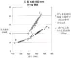
图19是对在多孔区域上方的InGaN LED而言,标准化电致发光(EL)强度对波长的图;Figure 19 is a graph of normalized electroluminescence (EL) intensity versus wavelength for an InGaN LED over a porous region;
图20是对在无孔基材上的InGaN LED而言,在不同电流引入时标准化电致发光(EL)强度对波长的图;Figure 20 is a graph of normalized electroluminescence (EL) intensity versus wavelength at different current introductions for InGaN LEDs on non-porous substrates;
图21是对生长在多孔区域上方的与图15相同的InGaN LED而言,在不同电流引入时标准化电致发光(EL)强度对波长的图;Figure 21 is a graph of normalized electroluminescence (EL) intensity versus wavelength at different current introductions for the same InGaN LED as in Figure 15 grown over a porous region;
图22是对在无孔基材上的不同像素大小的InGaN微型LED测得的I-V曲线,且该插入影像示出了黄光发射;Figure 22 is an I-V curve measured for InGaN micro-LEDs of different pixel sizes on a non-porous substrate, and the inset image shows yellow emission;
图23是对在多孔基材上的不同像素大小的InGaN微型LED测得的I-V曲线,且该插入影像示出了红光发射;Figure 23 is an I-V curve measured for InGaN micro-LEDs of different pixel sizes on a porous substrate, and the inset image shows red emission;
图24A是比较生长在不同模板上的三种LED的强度对EL波长的图;Figure 24A is a graph comparing intensity versus EL wavelength for three LEDs grown on different templates;
图24B是比较生长在不同模板上的三种LED的强度对EL波长的图;Figure 24B is a graph comparing intensity versus EL wavelength for three LEDs grown on different templates;
图24C是比较生长在不同模板上的两种LED的强度对EL波长的图。Figure 24C is a graph comparing intensity versus EL wavelength for two LEDs grown on different templates.
具体实施方式Detailed ways
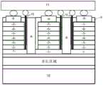
图1示出了适用于依据本发明的LED的多孔模板。Figure 1 shows a porous template suitable for an LED according to the invention.
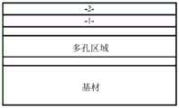
该多孔模板包括在基材上的III族-氮化物材料的多孔区域,且III族-氮化物材料的无孔层配置在该多孔区域的顶面上方。或者,可在该基材与该多孔区域之间具有III族-氮化物材料的其他层。The porous template includes a porous region of Ill-nitride material on a substrate, and a non-porous layer of Ill-nitride material is disposed over a top surface of the porous region. Alternatively, there may be an additional layer of Ill-nitride material between the substrate and the porous region.
如以下更详细所述地,该多孔区域可藉由磊晶地(epitaxially)生长III族-氮化物材料的n掺杂区域且接着生长III族-氮化物材料的未掺杂层及使用如国际专利申请案PCT/GB2017/052895(公开号为WO2019/063957)及PCT/GB2019/050213(公开号为WO2019/145728)中揭示的孔隙化过程使该n掺杂区域孔隙化来提供。As described in more detail below, the porous region can be prepared by epitaxially growing an n-doped region of III-nitride material and then growing an undoped layer of III-nitride material and using, for example, the International The porosity process disclosed in patent applications PCT/GB2017/052895 (publication number WO2019/063957) and PCT/GB2019/050213 (publication number WO2019/145728) provides porosity for the n-doped region.
如上所述,这孔隙化在晶格中产生应变松弛,这意味其他半导体层的后续增生受益于其晶格中的减少压力应变。As mentioned above, this porosity produces strain relaxation in the lattice, which means that subsequent growth of other semiconductor layers benefits from the reduced stress strain in their lattice.
该多孔区域可包括一层或多层一个或多个III族-氮化物材料且可具有一定范围的厚度,而全部仍提供使增生在该多孔区域上方的InGaN发光层的波长位移的应变松弛好处。在优选实施例中,该多孔区域可例如包括GaN和/或InGaN。The porous region may comprise one or more layers of one or more Ill-nitride materials and may have a range of thicknesses, all while still providing the benefit of strain relaxation to shift the wavelength of the InGaN emissive layer grown over the porous region . In a preferred embodiment, the porous region may eg comprise GaN and/or InGaN.
各种LED结构可增生在图1所示的模板上方。Various LED structures can be grown over the template shown in FIG. 1 .
具体而言,本领域技术人员已知的用于制造黄或绿光LED的包括InGaN发光层的LED结构可使用标准LED制造步骤增生在该多孔模板上。但是,当生长在该多孔模板上时,通常发射第一波长的LED结构发射红位移的较长波长。In particular, LED structures comprising an InGaN emitting layer known to those skilled in the art for fabricating yellow or green LEDs can be grown on the porous template using standard LED fabrication steps. However, typically the LED structure emitting at the first wavelength emits a red-shifted longer wavelength when grown on the porous template.
依此方式,使用III族-氮化物材料的多孔区域作为用于增生已知InGaN LED结构的模板或准基材容许较长波长LED以直接方式制成。In this way, the use of porous regions of Ill-nitride materials as templates or quasi-substrates for the growth of known InGaN LED structures allows longer wavelength LEDs to be fabricated in a straightforward manner.
在优选实施例中,依据本发明的LED包括以下层且可使用以下过程逐步地制造。In a preferred embodiment, an LED according to the invention comprises the following layers and can be fabricated stepwise using the following process.
该LED结构的以下说明涉及以由下向上的方式说明的顶发射架构,但本发明可同样地应用于底发射架构。The following description of the LED structure refers to a top-emitting architecture illustrated in a bottom-up manner, but the invention is equally applicable to bottom-emitting architectures.
图2-基材与用于孔隙化的III族-氮化物层Figure 2 - Substrate with III-Nitride layer for porosity
使用兼容基材作为用于磊晶生长的开始表面。该基材可为硅、蓝宝石、SiC、β-Ga2O3、GaN、玻璃或金属。该基材的晶体方位可为极性、半极性或非极性方位。该基材可具有1cm2、2英寸、4英寸、6英寸、8英寸、12英寸、16英寸直径及16英寸直径以上的不同尺寸,且该基材可具有大于1μm,例如在1μm至15000μm之间的厚度。Use compatible substrates as starting surfaces for epitaxial growth. The substrate can be silicon, sapphire, SiC, β-Ga2O3 , GaN, glass or metal. The crystallographic orientation of the substrate can be polar, semi-polar or non-polar. The substrate can have different sizes of 1 cm2 , 2 inches, 4 inches, 6 inches, 8 inches, 12 inches, 16 inches in diameter, and more than 16 inches in diameter, and the substrate can have a diameter greater than 1 μm, such as between 1 μm and 15000 μm between the thickness.
III族-氮化物材料的一层或层堆叠物在该基材上磊晶地生长。该III族-氮化物层可包括这些元素中的一者或其组合:Al、Ga、In(二元、三元或四元层)。A layer or stack of layers of Ill-nitride material is grown epitaxially on the substrate. The Ill-nitride layer may comprise one or a combination of these elements: Al, Ga, In (binary, ternary or quaternary layer).
该III族-氮化物堆叠物的厚度T优选地是至少10nm、至少50nm或至少100nm,例如在10至10000nm之间。The thickness T of the III-nitride stack is preferably at least 10 nm, at least 50 nm or at least 100 nm, for example between 10 and 10000 nm.
该III族-氮化物层包括具有在1×1017cm-3至5×1020cm-3间的n型掺杂浓度的掺杂区域。该III族-氮化物层亦可包括在该掺杂区域上方的III族-氮化物材料的未掺杂“覆盖”层。The III-nitride layer comprises a doped region with an n-type doping concentration between 1×1017 cm−3 and 5×1020 cm−3 . The Ill-nitride layer may also include an undoped "capping" layer of Ill-nitride material over the doped region.
该掺杂区域可终止在该III族-氮化物层的暴露上表面,在此情形中该层的该表面在电化学蚀刻时被孔隙化。The doped region may terminate at the exposed upper surface of the Ill-nitride layer, in which case the surface of the layer is voided upon electrochemical etching.
或者,该III族-氮化物材料的该掺杂区域被III族-氮化物材料的未掺杂“覆盖”层覆盖,使得该掺杂区域是该半导体结构中的次表面。该掺杂区域的次表面开始深度(d)可例如在1至2000nm之间。Alternatively, the doped region of the Ill-nitride material is covered by an undoped "capping" layer of Ill-nitride material such that the doped region is a subsurface in the semiconductor structure. The subsurface initiation depth (d) of the doped region may, for example, be between 1 and 2000 nm.
图3-对多孔区域的孔隙化Figure 3 - Porosification of porous regions
该III族-氮化物层(或层堆叠物)沉积在该基材上后,使它藉由如在国际专利申请案PCT/GB2017/052895(公开号为WO2019/063957)及PCT/GB2019/050213(公开号为WO2019/145728)中揭示的晶圆级孔隙化过程来孔隙化。在这过程中,该III族-氮化物材料的掺杂区域成为多孔,而没有任何III族-氮化物材料的未掺杂区域成为多孔。After the Group III-nitride layer (or layer stack) is deposited on the substrate, it is passed through as in the international patent application PCT/GB2017/052895 (publication number is WO2019/063957) and PCT/GB2019/050213 (Publication No. WO2019/145728) disclosed in the wafer-level porosity process to porosity. During this process, the doped regions of the Ill-nitride material become porous, while the undoped regions without any Ill-nitride material become porous.
该孔隙化步骤后,该结构因此包括仍有先前n掺杂III族-氮化物材料的多孔区域及任选的覆盖该多孔区域的无孔中间层。After the porosification step, the structure thus comprises a porous region of the previously n-doped Ill-nitride material and optionally a non-porous intermediate layer covering the porous region.
该多孔层的孔隙化程度是藉由该电化学蚀刻过程控制且可在1%至99%孔隙度之间、优选在20%至90%孔隙度之间或在30%至80%之间,但亦可使用更小或更大的孔隙度。The degree of porosity of the porous layer is controlled by the electrochemical etching process and may be between 1% to 99% porosity, preferably between 20% to 90% porosity or between 30% to 80%, but Smaller or larger porosities may also be used.
孔隙化后的多孔区域的厚度是优选地大于1nm、更优选地是大于10nm、特别优选地是至少40nm、50nm或100nm。但是,获得由该多孔区域提供的应变松弛好处所需的材料厚度可依据形成该多孔区域的III族-氮化物材料的种类改变。The thickness of the porosified porous region is preferably greater than 1 nm, more preferably greater than 10 nm, particularly preferably at least 40 nm, 50 nm or 100 nm. However, the material thickness required to obtain the strain relaxation benefits provided by the porous region may vary depending on the type of Ill-nitride material forming the porous region.
由该孔隙化过程产生的多孔区域可为在整层中具有均匀组成及均匀孔隙度的III族-氮化物材料的整体层。或者,该多孔区域可包括不同组成和/或孔隙度的多个多孔材料层,因此形成III族-氮化物材料的多孔堆叠物。例如,该多孔区域可为多孔GaN的连续层、多孔InGaN的连续层或包括一个或多个多孔GaN层和/或一个或多个多孔InGaN层的堆叠物。本发明人发现用于增生的该多孔区域的应变松弛好处可在具有不同厚度、组成或层状堆叠物的大范围多孔区域获得。The porous region resulting from this porosification process can be an integral layer of Ill-nitride material with uniform composition and uniform porosity throughout the layer. Alternatively, the porous region may comprise multiple layers of porous material of varying composition and/or porosity, thus forming a porous stack of Ill-nitride material. For example, the porous region may be a continuous layer of porous GaN, a continuous layer of porous InGaN, or a stack comprising one or more porous GaN layers and/or one or more porous InGaN layers. The present inventors have discovered that the strain relaxation benefits of this porous region for growth can be obtained over a wide range of porous regions with different thicknesses, compositions or layer stacks.
在图中所示的实施例中,该多孔区域是单一多孔层。In the embodiment shown in the figures, the porous region is a single porous layer.
当在该掺杂区域上方有III族-氮化物材料的未掺杂覆盖层时,在下方掺杂区域的穿过表面孔隙化后,该未掺杂区域保持无孔。这无孔覆盖层的厚度D可优选地为至少2nm、至少5nm或至少10nm且优选地为5nm至3000nm。在该掺杂区域上方提供未掺杂覆盖层有利地产生在孔隙化后覆盖该多孔区域的III族-氮化物材料的无孔层。这无孔覆盖层可有利地容许在该多孔区域上方更优选地增生其他材料。When there is an undoped capping layer of Ill-nitride material over the doped region, the undoped region remains non-porous after through-surface porosity of the underlying doped region. The thickness D of this non-porous covering layer may preferably be at least 2 nm, at least 5 nm or at least 10 nm and preferably between 5 nm and 3000 nm. Providing an undoped capping layer over the doped region advantageously results in a non-porous layer of Ill-nitride material covering the porous region after porosification. This non-porous cover layer may advantageously allow the growth of other materials, more preferably over the porous region.
当可在整个半导体晶圆上执行PCT/GB2017/052895(公开号为WO2019/063957)及PCT/GB2019/050213(公开号为WO2019/145728)的孔隙化方法时,不需要加工/图案化/处理来准备用于孔隙化的模板。When the porosification methods of PCT/GB2017/052895 (published as WO2019/063957) and PCT/GB2019/050213 (published as WO2019/145728) can be performed on the entire semiconductor wafer, no machining/patterning/handling is required to prepare the template for porosification.
图4-连接层Figure 4 - Connection layer
形成该多孔层后,可在由该多孔层及该无孔覆盖层提供的多孔模板/准基板上生长III族-氮化物LED磊晶结构。After forming the porous layer, the Ill-nitride LED epitaxial structure can be grown on the porous template/quasi-substrate provided by the porous layer and the non-porous cover layer.
用于在该模板上生长该LED结构的第一层可称为连接层1。The first layer used to grow the LED structure on the template may be referred to as
虽然LED磊晶结构可直接地生长在该无孔覆盖层上,但最好在增生该LED结构前在该覆盖层上方设置连接层1。本发明人发现使用在该多孔区域与该LED磊晶结构之间的III族-氮化物连接层1可有利地确保在该LED与该多孔模板/基材之间的良好磊晶关系。这层的生长确保在该连接层顶部的后续增生平顺且磊晶并且具有适当高质量。Although the LED epitaxial structure can be grown directly on the non-porous cover layer, it is preferable to place the
该连接层1是由III族-氮化物材料形成且可包括这些元素中的一者或其组合:Al、Ga、In(二元、三元或四元层)。The
该连接层可为掺杂或未掺杂层。该连接层可选择地掺杂适当n型掺杂剂材料,例如Si、Ge、C、O。该III族-氮化物层可具有在1×1017cm-3至5×1020cm-3之间的掺杂浓度。The connection layer can be a doped or undoped layer. The connection layer is optionally doped with a suitable n-type dopant material, eg Si, Ge, C, O. The III-nitride layer may have a doping concentration between 1×1017 cm−3 and 5×1020 cm−3 .
该连接层的厚度优选地是至少100nm且可例如在100nm至10000nm之间。The thickness of the connection layer is preferably at least 100 nm and may for example be between 100 nm and 10000 nm.
图5-n掺杂区域Figure 5-n-doped region
该连接层生长后,生长整体n掺杂III族-氮化物区域2。After growth of this connection layer, an integral n-doped Ill-
该n掺杂区域2可包括或由包括铟的III族-氮化物层或有或无铟的薄III族-氮化物层堆叠物构成,或生长铟的原子百分比在整个整体层或III族-氮化物层堆叠物中变化的该层或堆叠物。例如,该n掺杂区域可为n-GaN层或n-InGaN层,或者该n掺杂区域可为n-GaN/n-InGaN交替层堆叠物或在交替层中具有不同铟量的n-InGaN/n-InGaN交替层堆叠物。The n-doped
优选地,该n掺杂区域2包括铟,使得该n掺杂区域的结晶晶格具有与该LED中的InGaN发光层的晶格类似的晶格参数。该n掺杂区域中的铟原子百分比可例如在0.1%至25%之间变化。Preferably, the n-doped
在优选实施例中,n掺杂区域的铟含量是在该InGaN发光层的铟含量的20at%内、15at%内、10at%内或5at%内。这可有利地确保该n掺杂区域的晶格参数充分地类似该InGaN发光层的晶格参数以避免这些层间的过大应变。In preferred embodiments, the indium content of the n-doped region is within 20 at%, within 15 at%, within 10 at% or within 5 at% of the indium content of the InGaN light-emitting layer. This may advantageously ensure that the lattice parameter of the n-doped region is sufficiently similar to that of the InGaN light-emitting layer to avoid excessive strain between the layers.
该n掺杂区域的总厚度可为至少2nm、至少5nm、至少10nm或至少20nm。该n掺杂区域的厚度可例如在2nm至5000nm之间变化或甚至更厚。若该n掺杂区域包括一层堆叠物,则该堆叠物中的各独立层的厚度是优选地在1nm至40nm之间。The total thickness of the n-doped region may be at least 2 nm, at least 5 nm, at least 10 nm, or at least 20 nm. The thickness of the n-doped region can vary, for example, between 2 nm and 5000 nm or be even thicker. If the n-doped region comprises a stack, the thickness of each individual layer in the stack is preferably between 1 nm and 40 nm.
该n掺杂区域优选地具有在1×1017cm-3至5×1020cm-3间,优选地在1×1018cm-3至5×1020cm-3间,特别优选地大于1×1018cm-3的n型掺杂浓度。The n-doped region preferably has a thickness between 1×1017 cm-3 and 5×1020 cm-3 , preferably between 1×1018 cm-3 and 5×1020 cm-3 , particularly preferably greater than n-type doping concentration of 1×1018 cm-3 .
图6-发光区域Figure 6 - Light emitting area
生长该n掺杂区域2后,可生长底层、预成形层或预成形井(在图6中未标示)以便释放一个或多个发光层中的应变。该底层可为单一层或GaN、InGaN、GaN/InGaN或InGaN/InGaN的堆叠物/多个层。或者,该底层可具有类似InGaN QW/GaN量子障壁的结构,但具有较低铟比例。例如,在沉积具有比较高比例铟的发光层前,可生长由具有比该发光层低的铟比例的整体InGaN层构成的底层。或者,该底层可采用具有比该发光层低的铟比例的InGaN“假”QW及一个或多个GaN量子障壁的形式。After growing the n-doped
生长该n掺杂区域2及任选的该底层后,生长包括InGaN发光层的发光区域3。After growing the n-doped
该发光区域3可包括至少InGaN发光层。各InGaN发光层可为InGaN量子井(QW)。优选地,该发光区域可包括1个至7个的量子井。相邻量子井被具有与该量子井不同的组成的III族-氮化物材料的势垒层分开。The
一个或多个发光层在本文件中可称为“量子井”,但可采用各种不同形式。例如,该发光层可为InGaN的连续层,或该层可为连续、片段、间断层,可包括间隙或可具有纳米结构使得该量子井有效地包括表现为量子点的多个3D纳米结构。The one or more light emitting layers may be referred to in this document as "quantum wells", but may take a variety of different forms. For example, the light-emitting layer may be a continuous layer of InGaN, or the layer may be continuous, segmented, interrupted, may include gaps, or may have nanostructures such that the quantum well effectively includes 3D nanostructures behaving as quantum dots.
该量子井及障壁是在600℃至800℃的温度范围内生长。The quantum wells and barriers are grown at a temperature ranging from 600°C to 800°C.
各量子井由具有在15%至40%间的原子铟百分比的InGaN层构成。优选地,一个或多个发光氮化铟镓层和/或该量子井具有组成InxGa1-xN,其中0.05≤x≤0.35,优选地0.12≤x≤0.30或0.22≤x≤0.30,特别优选地0.22≤x≤0.27。Each quantum well consists of an InGaN layer with an atomic indium percentage between 15% and 40%. Preferably, the one or more luminescent InGaN layers and/or the quantum well has a compositionInxGa1-xN , where 0.05≤x≤0.35, preferably 0.12≤x≤0.30 or 0.22≤x≤0.30, Particularly preferably 0.22≦x≦0.27.
各量子井层的厚度可在1.5nm至8nm之间且优选在1.5nm至6nm之间或在1.5nm至4nm之间。该量子井可被薄的(0.5nm至3nm)III族-氮化物QW覆盖层覆盖,该III族-氮化物QW覆盖层可包括这些元素中的一者或其组合:Al、Ga、In(三元或四元层)。The thickness of each quantum well layer may be between 1.5nm and 8nm and preferably between 1.5nm and 6nm or between 1.5nm and 4nm. The quantum well can be covered by a thin (0.5nm to 3nm) Ill-nitride QW capping layer, which can include one or a combination of these elements: Al, Ga, In( ternary or quaternary layers).
在QW生长后立即添加的层的该QW覆盖层(若有的话)可为AlN、0.01%至99.9%中的任一Al%的AlGaN、GaN、0.01%至30%中的任一In%的InGaN。This QW capping layer (if any) for layers added immediately after QW growth can be AlN, any Al% from 0.01% to 99.9%, AlGaN, GaN, any In% from 0.01% to 30% InGaN.
分开该发光层(量子井)的该III族-氮化物QW势垒层可包括这些元素中的一者或其组合:Al、Ga、In(三元或四元层)。该QW势垒层可为AlN、0.01%至99.9%中的任一Al%的AlGaN、GaN及0.01%至15%中的任一In%的InGaN。优选地,该QW势垒层包括AlN和/或AlGaN。The Ill-nitride QW barrier layer separating the light emitting layer (quantum well) may comprise one or a combination of these elements: Al, Ga, In (ternary or quaternary layer). The QW barrier layer can be AlN, AlGaN of any Al% from 0.01% to 99.9%, GaN, and InGaN of any In% from 0.01% to 15%. Preferably, the QW barrier layer comprises AlN and/or AlGaN.
因为一个或多个QW覆盖层及QW障壁形成该发光区域3的一部分,所以这些层在图中未用独立符号表示。Since one or more QW capping layers and QW barriers form part of the
该QW覆盖层可在各QW后但在该障壁生长前生长。例如,若LED包括3个QW,则这些QW的各QW可增生QW覆盖层及接着QW势垒层,使得该发光区域包括3个如此的QW覆盖层及三个如此的QW势垒层。The QW capping layer can be grown after each QW but before the barrier growth. For example, if the LED comprises 3 QWs, each of these QWs can be augmented with a QW capping layer followed by a QW barrier layer such that the light emitting region includes 3 such QW capping layers and three such QW barrier layers.
1.可在与该QW相同的条件下生长该覆盖层。1. The cap layer can be grown under the same conditions as the QW.
2.可在无生长的情形下升温至较高温度且使这覆盖层生长(事实上这是退火步骤)并且在此该升温是在不同气体混合物中执行。2. It is possible to ramp up to a higher temperature without growth and grow this cap layer (in fact this is an annealing step) and here the ramping is performed in a different gas mixture.
3.可在温度上升期间升温及生长。3. It can heat up and grow during the temperature rise period.
该发光区域的设计可依据本领域技术人员非常了解且在LED设计中已知的参数来改变。例如,可依据该LED的目标EL发射波长,改变发光层及势垒层的组成、厚度及数目。如本申请案中先前所述地,当需要较长波长发射时,可增加InGaN发光层的铟含量。The design of the light emitting area can vary according to parameters well understood by those skilled in the art and known in LED design. For example, the composition, thickness and number of the light emitting layer and the barrier layer can be changed according to the target EL emission wavelength of the LED. As previously described in this application, the indium content of the InGaN light emitting layer can be increased when longer wavelength emission is desired.
如上所述,本发明可藉由在包括多孔区域的模板上方生长已知地在电偏压作用下发射第波长的已知LED结构来提供。由该LED结构下方的多孔区域产生的应变松弛可在相同生长条件下将更多铟加入一个或多个发光层,因此当相较于在相同条件下在无孔基材上方生长的相同LED结构时,制得的LED的波长产生红位移。因此可使用本发明获得比在已知技术中可能获得者更多样的发射波长,且特别地可在更高InGaN生长温度下获得较长波长。这导致了在该LED中优异质量的晶体结构,因此产生较高性能的LED。As noted above, the present invention can be provided by growing a known LED structure known to emit a second wavelength under an electrical bias, over a template comprising a porous region. The strain relaxation created by the porous region beneath the LED structure can incorporate more indium into the emissive layer(s) under the same growth conditions, so when compared to the same LED structure grown over a non-porous substrate under the same conditions, The wavelength of the LEDs produced is red-shifted. A greater variety of emission wavelengths can thus be obtained using the present invention than is possible in the known art, and in particular longer wavelengths can be obtained at higher InGaN growth temperatures. This results in a crystal structure of superior quality in the LED, thus resulting in a higher performance LED.
因为制造较长波长黄光、橙光或红光LED的先前尝试由于未加入足够铟而失败,所以对制造较长波长LED而言,一个或多个发光层中的大量铟使该覆盖层更为重要。因此覆盖对确保有足够铟存在该发光区域内是非常重要的。Because previous attempts to make longer wavelength yellow, orange, or red LEDs have failed due to not adding enough indium, for longer wavelength LEDs, a large amount of indium in one or more light-emitting layers makes the cover layer more durable. as important. Coverage is therefore very important to ensure that enough indium is present in the light emitting region.
图7-覆盖层Figure 7 - Overlay
在一个或多个发光层生长后,生长未掺杂覆盖层4。因为该未掺杂覆盖层4是在完整发光区域生长后,例如在QW、QW覆盖层及QW势垒层的堆叠物生长后形成,所以这层可称为发光区域覆盖层。After the growth of one or more light-emitting layers, an
该覆盖层(发光区域覆盖层)4是在用于III族-氮化物LED的生长架构中已知的标准层。This covering layer (light-emitting area covering layer) 4 is a standard layer known in growth architectures for III-nitride LEDs.
该覆盖层的厚度可在5nm至30nm之间,优选在5nm至25nm或5nm至20nm之间。The thickness of the covering layer may be between 5nm and 30nm, preferably between 5nm and 25nm or between 5nm and 20nm.
该未掺杂覆盖层4的目的是保护该发光区域(QW堆叠物)中的铟及防止它在后续处理时脱附/蒸发。因为该InGaN QW通常在对GaN/AlGaN不利的较低温度下生长,所以可在该发光区域上方生长其他层前通常需要温度升高步骤。该覆盖层是用于确保一个或多个InGaN发光层被适当地覆盖及保护,因此存在机会和时间窗来改变该p掺杂层生长条件以获得更好的材料质量。该发光区域覆盖层4亦确保无Mg掺杂物在生长p型层时进入该QW区域。The purpose of the
电子阻挡层(EBL)Electron blocking layer (EBL)
在生长量子井、覆盖及势垒层后,生长包括铝的III族-氮化物电子阻挡层(EBL)5。该Al%可例如在5%至25%之间,但亦可为更高Al含量。After growing the quantum well, capping and barrier layers, a group III-nitride electron blocking layer (EBL) 5 comprising aluminum is grown. This Al% may for example be between 5% and 25%, but also higher Al contents.
用适当p型掺杂材料掺杂该EBL。该EBL的p型掺杂浓度是优选地在5×1018cm-3至8×1020cm-3之间。The EBL is doped with an appropriate p-type dopant material. The p-type doping concentration of the EBL is preferably between 5×1018 cm−3 and 8×1020 cm−3 .
该EBL的厚度可在10nm至50nm之间,并且优选地为20nm。The thickness of the EBL may be between 10nm and 50nm, and is preferably 20nm.
图8-p掺杂层Figure 8 - p-doped layer
在该电子阻挡层(EBL)5上方生长p掺杂层6。A p-doped
优选地用Mg掺杂该p型区域,且该p型层的p型掺杂浓度优选地在5×1018cm-3至8×1020cm-3之间。The p-type region is preferably doped with Mg, and the p-type doping concentration of the p-type layer is preferably between 5×1018 cm−3 and 8×1020 cm−3 .
该p掺杂III族-氮化物层可包括In与Ga。The p-doped Ill-nitride layer may include In and Ga.
该掺杂层的厚度是优选地在20nm至200nm之间,特别优选地在50nm至100nm之间。掺杂浓度在该p型层上各处可不同且可在该层朝向该LED表面的最后10nm至30nm中具有掺杂浓度的峰值以获得更好的p接触。The thickness of the doped layer is preferably between 20 nm and 200 nm, particularly preferably between 50 nm and 100 nm. The doping concentration can vary throughout on the p-type layer and can have a peak of doping concentration in the last 10nm to 30nm of the layer towards the LED surface for better p-contact.
为了活化该p掺杂层中的Mg受子,该结构可在MOCVD反应器内或在退火炉中退火。在N2中或在N2/O2的环境中该退火温度可在700℃至850℃的范围内。To activate the Mg acceptors in the p-doped layer, the structure can be annealed in an MOCVD reactor or in an annealing furnace. The annealing temperature may be in the range of 700°C to 850°C inN2 or in aN2 /O2 environment.
因为该EBL及该p掺杂层都被p型掺杂,所以这些层可称为p掺杂区域。Since both the EBL and the p-doped layer are doped p-type, these layers may be referred to as p-doped regions.
图9-透明导电层Figure 9 - Transparent Conductive Layer
用透明导电层7覆盖活性半导体层的堆叠物。该透明导电层可由Ni/Au、氧化铟锡、氧化铟锌、石墨烯、Pd、Rh、银、ZnO等或这些材料的组合形成。The stack of active semiconductor layers is covered with a transparent
该透明导电层的厚度可在10nm至250nm之间。The thickness of the transparent conductive layer can be between 10nm and 250nm.
透明导电层在所属技术领域中是已知的且可使用任何适当材料及厚度。Transparent conductive layers are known in the art and any suitable material and thickness can be used.
可能需要退火步骤来产生该p接触欧姆。An annealing step may be required to create this p-contact ohm.
图10Figure 10
依据制成的LED结构,该半导体结构可被处理成LED、小型LED或微型LED。Depending on the fabricated LED structure, the semiconductor structure can be processed as an LED, mini-LED or micro-LED.
一般的LED通常比200μm(是指该LED结构的宽度及长度的横向尺寸大。小型LED的横向大小通常是100μm至200μm,而微型LED的大小通常小于100μm。General LEDs are usually larger than 200 μm (referring to the width and length of the LED structure in lateral dimension. The lateral size of small LEDs is usually 100 μm to 200 μm, while the size of micro LEDs is usually less than 100 μm.
由图10开始示出了将该半导体结构的层2至7蚀刻成各具有相同结构的多个独立LED堆叠物或台面后的半导体结构。The semiconductor structure after etching
LED制造的步骤是已知的且为本领域技术人员所熟知。对本发明而言,以下制造步骤的顺序非特定且本领域技术人员可了解在本发明的范围内的LED装置可使用以下所示者的替代制造步骤来制备。但是,只是为了说明,以下说明依据本发明制备LED的优选制造行程。The steps of LED fabrication are known and familiar to those skilled in the art. The order of the following fabrication steps is not specific to the present invention and those skilled in the art will appreciate that LED devices within the scope of the present invention can be fabricated using alternative fabrication steps as shown below. However, for purposes of illustration only, the following describes a preferred fabrication sequence for preparing LEDs according to the present invention.
在下一步骤中,建构该透明导电层7使得它只覆盖该活性发射组件的顶面。该建构可使用包括抗蚀剂涂布及光微影的标准半导体处理方法来达成。该透明导电层是藉由使用湿式化学或使用氩的溅镀蚀刻过程来蚀刻。这步骤后进行该III族-氮化物结构的湿式或干式蚀刻。使用电感耦合反应离子蚀刻、只有反应离子蚀刻过程或中性束蚀刻在该III族-氮化物层中产生多个台面。该干式蚀刻过程可包括Cl、Ar、BCl3、SiCl4气体中的任一个或多个。In a next step, the transparent
这步骤的目的是隔离该个别发射组件及进接该p-n接面的埋入n掺杂层。The purpose of this step is to isolate the individual emitter element and the buried n-doped layer accessing the p-n junction.
在该干式蚀刻过程后进行湿式蚀刻过程以便由该台面的侧壁移除干式蚀刻破坏。该湿式化学法可包括KOH(1%至20%)、TMAH或其他基础化学法。A wet etch process is performed after the dry etch process to remove dry etch damage from the sidewalls of the mesas. The wet chemistry can include KOH (1% to 20%), TMAH or other basic chemistry.
图11-钝化Figure 11 - Passivation
下一步骤是沉积钝化层8或钝化层的组合。该开始钝化层可为Al2O3(10nm至100nm)(藉由原子层沉积来沉积),接着溅镀或电浆加强化学蒸汽沉积SiO2、SiN或SiON(50nm至300nm)。The next step is to deposit a
该Al2O3可在50℃至150℃之间沉积。The Al2 O3 can be deposited between 50°C and 150°C.
该SiO2、SiN及SiON可在250℃至350℃之间沉积。The SiO2 , SiN and SiON can be deposited between 250°C and 350°C.
该溅镀过程可在室温下进行。The sputtering process can be performed at room temperature.
图12至13Figures 12 to 13
下一步骤是在该氧化物钝化层8中产生通孔以暴露该LED结构的顶部。这可透过湿式、干式蚀刻或两者的组合来达成。The next step is to create vias in the
就湿式缓冲氧化物蚀刻而言,可使用稀氢氟酸、磷酸或这些酸的混合物。For wet buffered oxide etching, dilute hydrofluoric acid, phosphoric acid, or mixtures of these acids can be used.
亦在该LED结构之间蚀刻信道穿过该连接层1,接着藉由在该通道中沉积介电掩模材料8使该LED结构互相电气地隔离,使得该LED可互相独立地操作。Channels are also etched through the
装置制造中的下一步骤是用金属层9覆盖该p掺杂层6上的透明导电层7以作为电p接触。该覆盖可藉由单一步骤或多个步骤来达成。该金属可完全地或部分地覆盖该像素。在这示例中使用单一步骤来简化细节。The next step in device fabrication is to cover the
该金属可包括Ti、Pt、Pd、Rh、Ni、Au。该完成金属堆叠物的厚度可在200nm至2000nm之间。The metal may include Ti, Pt, Pd, Rh, Ni, Au. The thickness of the finished metal stack may be between 200nm and 2000nm.
图14-暴露连接层Figure 14 - Exposing the connection layer
可使用标准光微影技术在该第二掩模(mask)层8中产生通孔以暴露该连接层1的多个区域。该通孔的大小可在200nm至50000nm之间变化。该通孔间的距离可在500nm至30000nm之间。该通孔只在未被LED结构占据的晶圆的区域中产生。Vias can be created in the
最好使用干式蚀刻来使用氟基气体蚀刻该第二掩模层8。The
图15-n接触Figure 15-n contact
装置制造中的下一步骤是藉由金属接触10覆盖该氧化物8中的通孔以进接与该LED结构的n掺杂层电接触的连接层1。该覆盖可藉由单一步骤或多个步骤来达成。该金属可完全地或部分地覆盖该像素。在这示例中使用单一步骤来简化细节。The next step in device fabrication is to cover the vias in the
该金属可包括Ti、Pt、Pd、Rh、Ni、Au。该完成金属堆叠物的厚度可在200nm至2000nm之间。The metal may include Ti, Pt, Pd, Rh, Ni, Au. The thickness of the finished metal stack may be between 200nm and 2000nm.
图16至图18Figure 16 to Figure 18
这处理后,可使该基材薄化和/或可移除该多孔区域使该连接层1暴露。After this treatment, the substrate can be thinned and/or the porous region can be removed to expose the
在该基材上且在该多孔区域或层1可进行表面结构化或粗化以增加光输出且控制该发射角度及其他光学工程及设计。Surface structuring or roughening can be done on the substrate and in the porous region or
最后,可将该晶圆/装置翻转且结合在可为硅/蓝宝石或任一种作为被动装置者的另一载体基材,或者可将该装置结合在用于活性矩阵微型LED示出了面板的CMOS硅底板上。Finally, the wafer/device can be flipped over and bonded to another carrier substrate which can be silicon/sapphire or either as a passive device, or the device can be bonded to a panel for active matrix micro LED display CMOS silicon substrate.
如图16所示,可将该装置的顶侧结合在另一载体晶圆/基材/底板11或微驱动电路板上以形成一像素的阵列。As shown in FIG. 16, the top side of the device can be bonded to another carrier wafer/substrate/
如图17所示,接着可由该装置移除该基材,且可将该装置的底侧可结合在盖玻璃或透明材料12上。The substrate can then be removed from the device and the bottom side of the device can be bonded to a cover glass or
如图18所示,可由该装置移除该基材及该多孔与无孔区域。该装置的顶侧可结合在另一载体晶圆/基材/底板11或微驱动电路板上以形成一像素的阵列。该装置的底侧可结合在盖玻璃或透明材料12上。As shown in Figure 18, the substrate and the porous and non-porous regions can be removed by the device. The top side of the device can be bonded to another carrier wafer/substrate/
本领域技术人员可了解的是该独立LED结构的发射波长可藉由依据LED构造的已知原理改变该LED结构的组成及层结构来控制。因此可使用本发明提供在不同发射波长范围内发射的各种可变波长LED装置,且可提供绿至红以外的颜色组合。Those skilled in the art will appreciate that the emission wavelength of the individual LED structures can be controlled by varying the composition and layer structure of the LED structures according to known principles of LED construction. The present invention can thus be used to provide a variety of variable wavelength LED devices emitting in different emission wavelength ranges, and can provide color combinations other than green to red.
图19至图23Figure 19 to Figure 23
图19示出了在多孔层上方的InGaN LED的示例,其由于由该多孔区域产生的波长红位移而发射大约625nm的峰波长。Figure 19 shows an example of an InGaN LED above a porous layer emitting a peak wavelength of approximately 625 nm due to the wavelength red shift produced by the porous region.
图20与图21比较无孔基材(图20)上的InGaN LED与在包括III族-氮化物材料的多孔层的模板上生长的相同InGaN LED的发射特性。这两个图的比较证明朝向由该多孔底层产生的较长发射波长的位移,因为该多孔模板上的LED的发射波长是比该无孔模板上的相同LED的发射波长一致地长21nm与45nm之间。Figure 20 compares with Figure 21 the emission characteristics of an InGaN LED on a non-porous substrate (Figure 20) and the same InGaN LED grown on a template comprising a porous layer of Ill-nitride material. A comparison of these two figures demonstrates a shift towards longer emission wavelengths produced by the porous substrate, as the emission wavelength of the LED on the porous template is consistently 21 nm and 45 nm longer than the emission wavelength of the same LED on the non-porous template between.
图22与图23比较无孔基材(图22)上的黄光InGaN微型LED与在包括多孔层的模板上的红光InGaN微型LED的I-V特性。Figure 22 and Figure 23 compare the I-V characteristics of a yellow InGaN micro-LED on a non-porous substrate (Figure 22) and a red InGaN micro-LED on a template including a porous layer.
图24A至图24CFigure 24A to Figure 24C
图24A至图24C的实验是对晶圆上芯片(CoW)LED执行以测试蓝光、绿光及黄光波长的波长位移。The experiments of FIGS. 24A-24C were performed on chip-on-wafer (CoW) LEDs to test the wavelength shift of blue, green, and yellow wavelengths.
图24A至图24C是发光强度或亮度对由晶圆上芯片微型LED的阵列发射的峰EL发射波长的图。图24A至图24C是由配置成发射在400nm与600nm之间的各种EL波长的LED获得,显示本发明的红位移效应是通过具有不同发射波长的大范围LED获得。24A-24C are graphs of luminous intensity or brightness versus peak EL emission wavelength emitted by an array of chip-on-wafer microLEDs. Figures 24A-24C were obtained with LEDs configured to emit at various EL wavelengths between 400nm and 600nm, showing that the red shift effect of the present invention is obtained with a wide range of LEDs having different emission wavelengths.
在图24A中,测试在GaN及平坦蓝宝石基材(FSS)上生长的标准450nm LED A且发现在电偏压作用下主要在440至450nm的范围中发光。LED A的数据是显示在图24A中的粉红色数据点中。In Fig. 24A, a standard 450nm LED A grown on GaN and flat sapphire substrate (FSS) was tested and found to emit mainly in the 440 to 450nm range under electrical bias. The data for LED A is shown in the pink data points in Figure 24A.
在无孔GaN模板上生长已知以大约420nm发光的LED结构LED B。如图19A所示,LEDB在电偏压作用下以大约425nm至425nm发光。LED B的数据是显示在图24A中的深红色数据点中。LED B, an LED structure known to emit light at approximately 420 nm, was grown on a non-porous GaN template. As shown in Figure 19A, the LEDB emits light at about 425nm to 425nm under an electrical bias. The data for LED B is shown in the dark red data points in Figure 24A.
为了说明由本发明提供的波长红位移,在包括多孔GaN区域的模板上生长具有与LED B相同的LED结构的LED C。LED C的数据是显示在图24A中的绿色数据点中。选择LED B(在无孔基材上发射大约420nm的峰波长)作为用于达成为LED C提供在430nm至450nm范围内的峰EL发射波长的目标的适当LED结构,使得LED C增生在该多孔模板上时在可见光谱的紫光区域中发光。To illustrate the wavelength-red shift provided by the present invention, LED C with the same LED structure as LED B was grown on a template comprising porous GaN regions. The data for LED C is shown in the green data points in Figure 24A. LED B (emitting a peak wavelength of approximately 420 nm on a non-porous substrate) was chosen as an appropriate LED structure for the goal of providing LED C with a peak EL emission wavelength in the range of 430 nm to 450 nm, such that LED C was grown on the porous template emits light in the violet region of the visible spectrum.
LED B与LED C具有相同LED结构(相同活性区域及n与p型区域)且在相同磊晶生长操作中在相同生长条件下生长。但是,如图24A所示,LED C形成在多孔区域上方的事实导致发射行为的明显差异。首先,相较于420nm,多孔GaN上的LED C在430nm至445nm的范围中发射比LED B长的波长。在该多孔区域上方的增生因此对在该阵列中的LED造成平均大约10至25nm的波长红位移。其次,由于增生在该应变松弛多孔区域上方的半导体层的改良质量,在多孔GaN模板而非无孔模板上方形成LED C导致LED发射强度明显增加。LED B and LED C have the same LED structure (same active region and n and p-type regions) and were grown under the same growth conditions in the same epitaxial growth operation. However, as shown in Figure 24A, the fact that LED C is formed over the porous region results in a clear difference in emission behavior. First, LED C on porous GaN emits a longer wavelength than LED B in the range of 430nm to 445nm compared to 420nm. Growth over the porous region thus causes an average wavelength red shift of about 10 to 25 nm for the LEDs in the array. Second, forming LED C over a porous GaN template rather than a non-porous template results in a significant increase in LED emission intensity due to the improved quality of the semiconductor layer grown over this strain-relaxed porous region.
在图24B中,标准绿光LED“D”生长在无孔GaN模板上,且发现在电偏压作用下主要在510nm至530nm的范围中发光。LED D的数据是显示在图24B中的绿色数据点中。In Figure 24B, a standard green LED "D" was grown on a non-porous GaN template and was found to emit primarily in the 510nm to 530nm range under electrical bias. The data for LED D is shown in the green data points in Figure 24B.
相同绿光LED结构增生在包括多孔GaN层的类似GaN模板上以形成LED E。LED E的数据是显示在图19B中的深红色数据点中。由于增生在该应变松弛多孔区域上方的半导体层的改良质量产生的红位移,相较于LED D的520nm发射波长,发现LED E以平均540nm至560nm的较长波长发光。The same green LED structure was grown on a similar GaN template including a porous GaN layer to form LED E. The data for LED E is shown in the dark red data points in Figure 19B. LED E was found to emit at a longer wavelength averaging 540nm to 560nm compared to the 520nm emission wavelength of LED D due to the red shift resulting from the improved quality of the semiconductor layer grown over this strain relaxed porous region.
图24C示出了LED F的比较数据,该LED F是已知在电偏压作用下以大约540nm至560nm发光的LED结构。LED F的数据是显示在图24C中的蓝色数据点中。Figure 24C shows comparative data for LED F, an LED structure known to emit light at approximately 540 nm to 560 nm under electrical bias. The data for LED F is shown in the blue data points in Figure 24C.
为了说明由本发明提供的波长红位移,在包括多孔GaN区域的模板上生长具有与LED F相同的LED结构的LED G。LED G的数据是显示在图24C中的暗红色数据点中。选择LEDF(在无孔基材上发射大约540nm至560nm的峰波长)作为用于达成为LED G提供在550nm至570nm范围内的峰EL发射波长的目标的适当LED结构,使得LED G增生在该多孔模板上时在可见光谱的绿光区域中发光。To illustrate the wavelength-red shift provided by the present invention, LED G with the same LED structure as LED F was grown on a template comprising porous GaN regions. The data for LED G is shown in the dark red data points in Figure 24C. LEDF (emitting a peak wavelength of approximately 540nm to 560nm on a non-porous substrate) was chosen as an appropriate LED structure for the goal of providing LED G with a peak EL emission wavelength in the range of 550nm to 570nm such that LED G grows on this porous template Glows in the green region of the visible spectrum when on.
LED F与LED G具有相同LED结构(相同活性区域及n与p型区域)且在相同磊晶生长操作中在相同生长条件下生长。但是,如图24C所示,LED G形成在一多孔区域上方的事实意味相较于540nm至560nm,多孔GaN上的LED G在550nm至570nm的范围中发射比LED F长的波长。因为由该多孔区域产生的应变松弛容许LED G在相同生长条件下加入比LED F多的铟,所以LEG G产生较长波长发射。LED F and LED G have the same LED structure (same active region and n and p-type regions) and were grown under the same growth conditions in the same epitaxial growth operation. However, as shown in FIG. 24C , the fact that LED G is formed over a porous region means that LED G on porous GaN emits a longer wavelength than LED F in the range of 550nm to 570nm compared to 540nm to 560nm. LEG G produces longer wavelength emission because the strain relaxation created by the porous region allows LED G to incorporate more indium than LED F under the same growth conditions.
Claims (61)
Translated fromChineseApplications Claiming Priority (21)
| Application Number | Priority Date | Filing Date | Title |
|---|---|---|---|
| GBGB2012108.3AGB202012108D0 (en) | 2020-08-04 | 2020-08-04 | Semiconductor structure |
| GBGB2012103.4AGB202012103D0 (en) | 2020-08-04 | 2020-08-04 | Semiconductor structure |
| GB2012110.9 | 2020-08-04 | ||
| GB2012103.4 | 2020-08-04 | ||
| GB2012105.9 | 2020-08-04 | ||
| GBGB2012110.9AGB202012110D0 (en) | 2020-08-04 | 2020-08-04 | Semiconductor structure |
| GBGB2012098.6AGB202012098D0 (en) | 2020-08-04 | 2020-08-04 | Semiconductor structure |
| GB2012108.3 | 2020-08-04 | ||
| GB2012098.6 | 2020-08-04 | ||
| GBGB2012105.9AGB202012105D0 (en) | 2020-08-04 | 2020-08-04 | Semiconductor structure |
| GBGB2018016.2AGB202018016D0 (en) | 2020-11-16 | 2020-11-16 | Red led and method of manufacture |
| GB2018016.2 | 2020-11-16 | ||
| PCT/GB2021/050158WO2021148813A1 (en) | 2020-01-22 | 2021-01-22 | Semiconductor structure and method of manufacture |
| GBPCT/GB2021/050147 | 2021-01-22 | ||
| GBPCT/GB2021/050152 | 2021-01-22 | ||
| GBPCT/GB2021/050158 | 2021-01-22 | ||
| PCT/GB2021/050147WO2021148803A1 (en) | 2020-01-22 | 2021-01-22 | Micro-led and manufacturing method thereof |
| PCT/GB2021/050152WO2021148808A1 (en) | 2020-01-22 | 2021-01-22 | Red led and method of manufacture |
| GBGB2110882.4AGB202110882D0 (en) | 2020-08-04 | 2021-07-28 | LED and method of manufacture |
| GB2110882.4 | 2021-07-28 | ||
| PCT/GB2021/052020WO2022029434A1 (en) | 2020-08-04 | 2021-08-04 | Led device and method of manufacturing an led device |
Publications (1)
| Publication Number | Publication Date |
|---|---|
| CN116250091Atrue CN116250091A (en) | 2023-06-09 |
Family
ID=80120107
Family Applications (1)
| Application Number | Title | Priority Date | Filing Date |
|---|---|---|---|
| CN202180067709.1APendingCN116250091A (en) | 2020-08-04 | 2021-08-04 | LED device and method of manufacturing LED device |
Country Status (7)
| Country | Link |
|---|---|
| US (1) | US20230290903A1 (en) |
| EP (2) | EP4608102A2 (en) |
| JP (1) | JP2023536361A (en) |
| KR (1) | KR20230058638A (en) |
| CN (1) | CN116250091A (en) |
| TW (1) | TW202221938A (en) |
| WO (1) | WO2022029434A1 (en) |
Families Citing this family (5)
| Publication number | Priority date | Publication date | Assignee | Title |
|---|---|---|---|---|
| EP4378003A1 (en)* | 2021-07-28 | 2024-06-05 | Poro Technologies Ltd | Led display device, method of controlling the same, and method of manufacturing a led display device |
| GB202213149D0 (en) | 2022-09-08 | 2022-10-26 | Poro Tech Ltd | Method of separating a semiconductor device from a substrate |
| GB202213939D0 (en) | 2022-09-23 | 2022-11-09 | Poro Tech Ltd | Monolithic array of semiconductor devices, display device, template wafer and method of manufacture |
| GB202216889D0 (en) | 2022-11-11 | 2022-12-28 | Poro Tech Ltd | Opto-electronic device and method of manufacturing |
| GB202218165D0 (en) | 2022-12-02 | 2023-01-18 | Poro Tech Ltd | Opto-electronic device having an electrical interconnection layer |
Family Cites Families (10)
| Publication number | Priority date | Publication date | Assignee | Title |
|---|---|---|---|---|
| KR100691444B1 (en)* | 2005-11-19 | 2007-03-09 | 삼성전기주식회사 | Nitride semiconductor light emitting device |
| US7928448B2 (en)* | 2007-12-04 | 2011-04-19 | Philips Lumileds Lighting Company, Llc | III-nitride light emitting device including porous semiconductor layer |
| KR20130066870A (en)* | 2011-12-13 | 2013-06-21 | 삼성전자주식회사 | Semiconductor light emitting device |
| JP6058946B2 (en)* | 2012-08-24 | 2017-01-11 | 学校法人 名城大学 | Nitride semiconductor device having a plurality of active layers, nitride semiconductor light emitting device, nitride semiconductor light receiving device, and method for manufacturing nitride semiconductor device |
| JP2014187159A (en)* | 2013-03-22 | 2014-10-02 | Rohm Co Ltd | Semiconductor light-emitting element |
| US10734545B2 (en)* | 2017-06-21 | 2020-08-04 | The Regents Of The University Of Michigan | Monolithically integrated InGaN/GaN quantum nanowire devices |
| US20200152841A1 (en)* | 2017-07-31 | 2020-05-14 | Yale University | Nanoporous micro-led devices and methods for making |
| KR102591874B1 (en) | 2017-09-27 | 2023-10-20 | 캠브리지 엔터프라이즈 리미티드 | Method for porosifying a material and semiconductor structure |
| GB201801337D0 (en) | 2018-01-26 | 2018-03-14 | Cambridge Entpr Ltd | Method for etching a semiconductor structure |
| CN108520911A (en)* | 2018-04-11 | 2018-09-11 | 山东大学 | A preparation method of InGaN-based blue light-emitting diode with nanoporous GaN distributed Bragg reflector |
- 2021
- 2021-08-03TWTW110128574Apatent/TW202221938A/enunknown
- 2021-08-04USUS18/040,542patent/US20230290903A1/enactivePending
- 2021-08-04EPEP25189661.9Apatent/EP4608102A2/enactivePending
- 2021-08-04CNCN202180067709.1Apatent/CN116250091A/enactivePending
- 2021-08-04EPEP21752135.0Apatent/EP4193392B1/enactiveActive
- 2021-08-04WOPCT/GB2021/052020patent/WO2022029434A1/ennot_activeCeased
- 2021-08-04KRKR1020237007769Apatent/KR20230058638A/enactivePending
- 2021-08-04JPJP2023507872Apatent/JP2023536361A/enactivePending
Also Published As
| Publication number | Publication date |
|---|---|
| EP4193392A1 (en) | 2023-06-14 |
| US20230290903A1 (en) | 2023-09-14 |
| KR20230058638A (en) | 2023-05-03 |
| TW202221938A (en) | 2022-06-01 |
| EP4193392B1 (en) | 2025-07-16 |
| EP4608102A2 (en) | 2025-08-27 |
| WO2022029434A1 (en) | 2022-02-10 |
| JP2023536361A (en) | 2023-08-24 |
Similar Documents
| Publication | Publication Date | Title |
|---|---|---|
| US20230053144A1 (en) | Red led and method of manufacture | |
| CN101689586B (en) | Nitride semiconductor light emitting element and method for manufacturing nitride semiconductor | |
| JP4872450B2 (en) | Nitride semiconductor light emitting device | |
| CN116250091A (en) | LED device and method of manufacturing LED device | |
| JP2010153838A (en) | Nitride semiconductor light emitting element and manufacturing method of the same | |
| CN113875030B (en) | Light-emitting diode precursor including a passivation layer | |
| JP2023510976A (en) | Micro LED and its manufacturing method | |
| TW202221937A (en) | Led device and method of manufacture | |
| CN100452456C (en) | Nitride semiconductor light emitting device and method for manufacturing the same | |
| US20090057694A1 (en) | Light optoelectronic device and forming method thereof | |
| CN112802869A (en) | White light LED with adjustable single-chip integrated nitride light-emitting wavelength and preparation method thereof | |
| TW202226617A (en) | Red led and method of manufacture | |
| JP2007201146A (en) | Light emitting element and its manufacturing method |
Legal Events
| Date | Code | Title | Description |
|---|---|---|---|
| PB01 | Publication | ||
| PB01 | Publication | ||
| SE01 | Entry into force of request for substantive examination | ||
| SE01 | Entry into force of request for substantive examination |